Introduction
At the end of 2024, Xiaomi officially announced the full opening of its Surge fast-charging technology, aiming to foster a more robust fast-charging ecosystem through cross-vendor collaboration. This initiative marks a gradual transition of Xiaomi’s proprietary charging protocols toward standardization and openness, providing new momentum for coordinated industry development. Meanwhile, as one of the brand’s established power tiers, the 33W charger continues to be widely deployed as a bundled adapter across multiple entry-level devices.
The unit disassembled in this review is the EU version of the Xiaomi 33W original in-box charger. It supports Xiaomi’s proprietary fast-charging protocol and is compatible with the PD 3.0 fast-charging standard. Below, we take a closer look at the materials and build quality of this charger.
Product Appearance
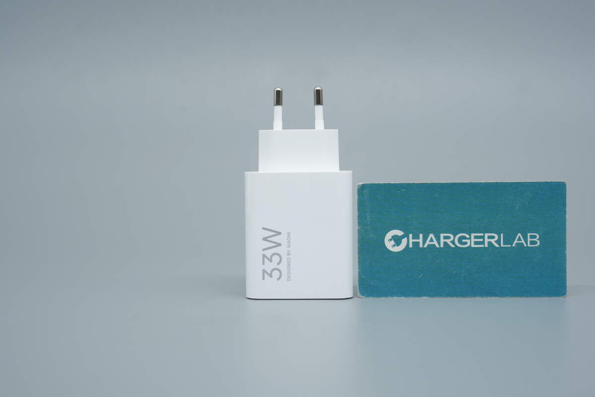
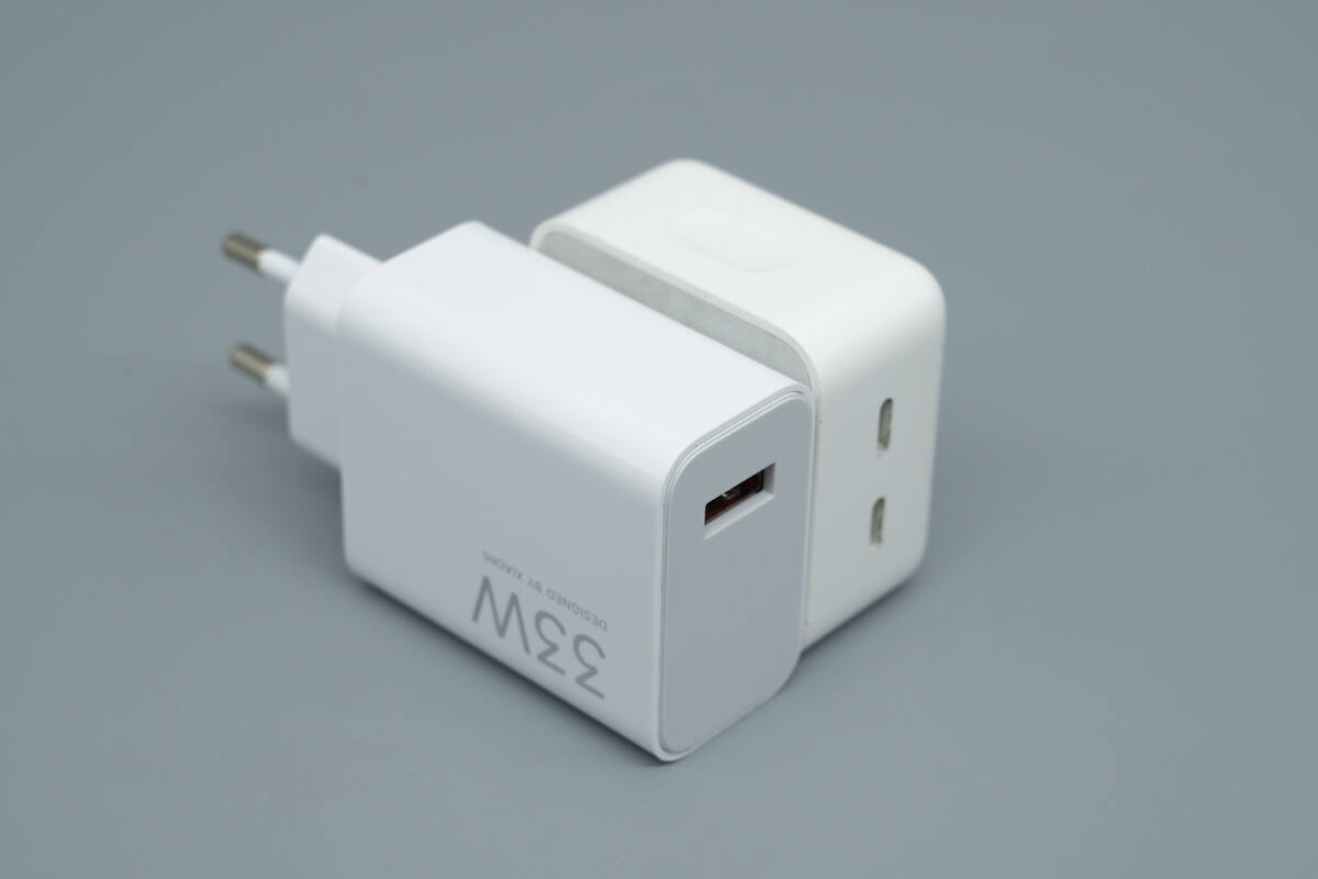
The charger features a glossy white finish, with “33W” printed on the enclosure, and is equipped with EU-standard prongs.
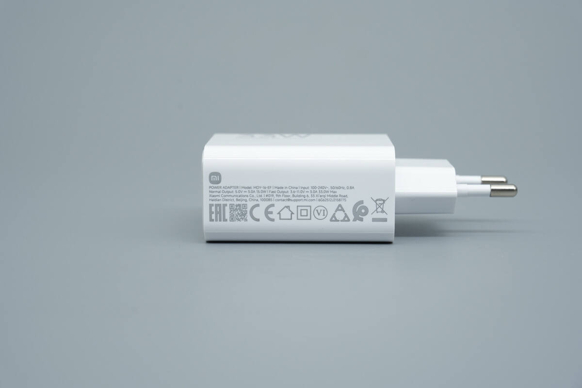
The specifications are printed on the side of the enclosure.
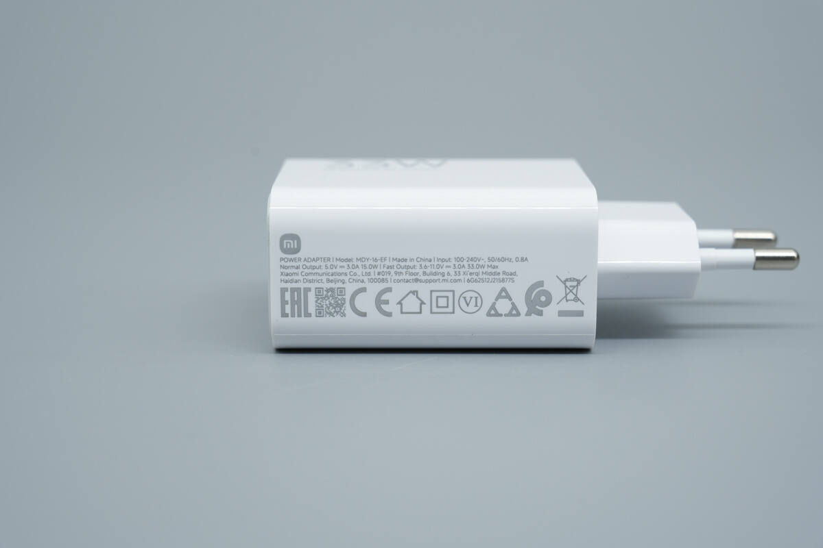
Model: MDY-16-EF
Input: 100–240V~ 50/60Hz 0.8A
Standard Output: 5V 3A 15.0W
Fast Charging Output: 3.6–11.0V 3A 33.0W Max
Manufacturer: Xiaomi Communications Technology Co., Ltd.
This product is certified with CE, EAC, and Level VI energy efficiency.
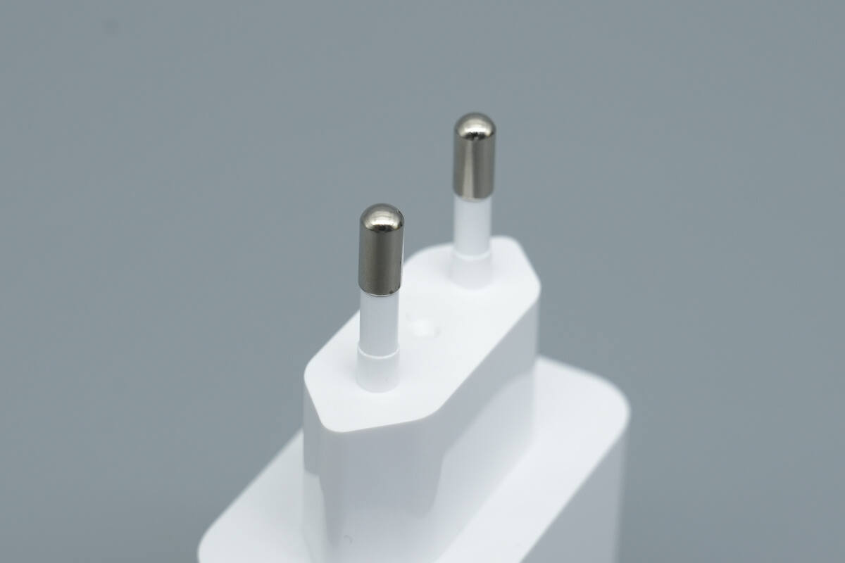
Close-up of the prongs.

It features a single USB-A port.
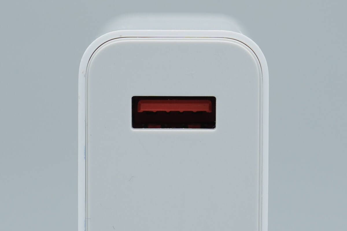
The USB-A port features an orange plastic insert, and the four internal spring contacts are widened for improved conductivity.
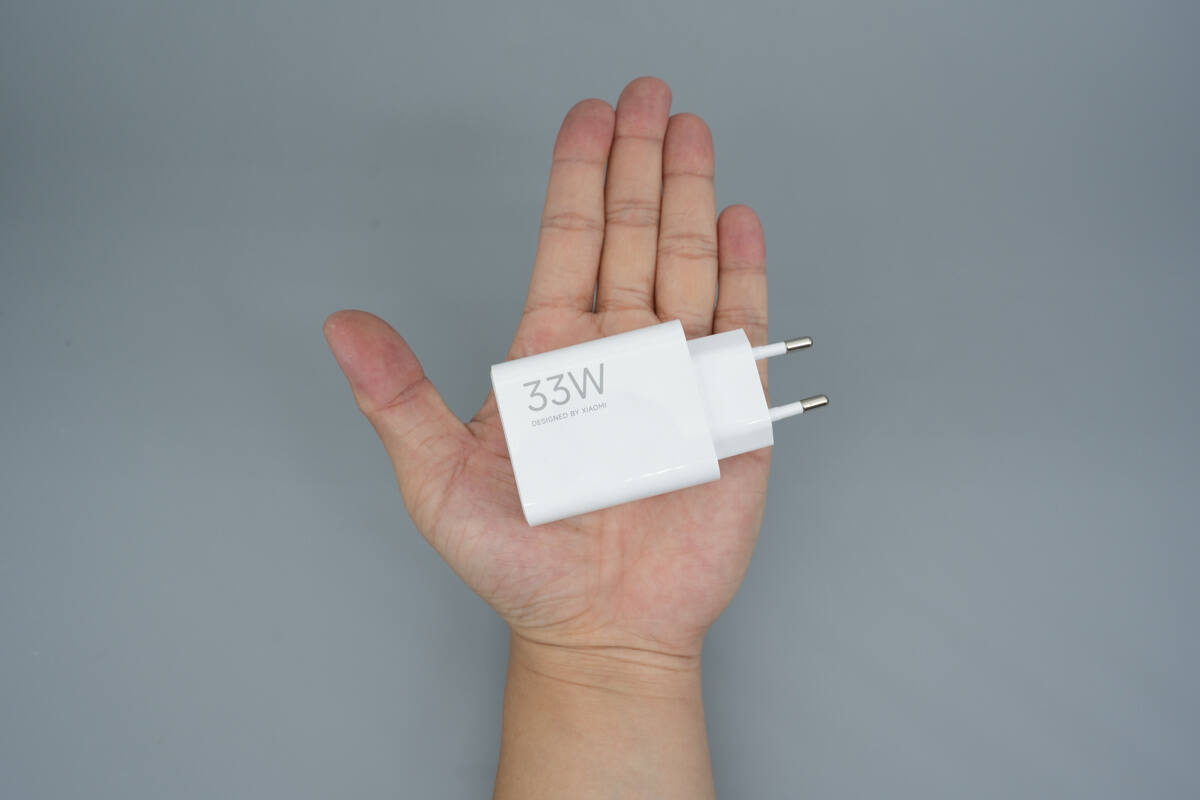
That's how big it is in the hand.
As shown, its size is compared with the Apple 35W Dual USB‑C charger.
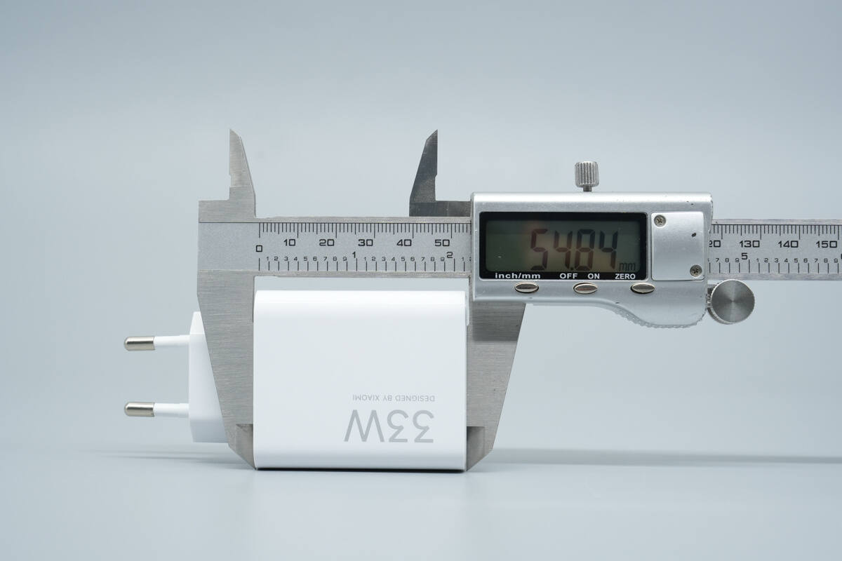
The length of the charger is about 54.84 mm (2.16 inches).
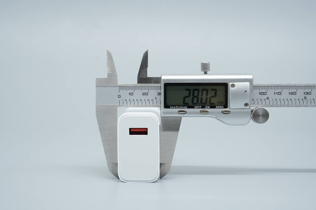
The width is about 28.02 mm (1.1 inches).
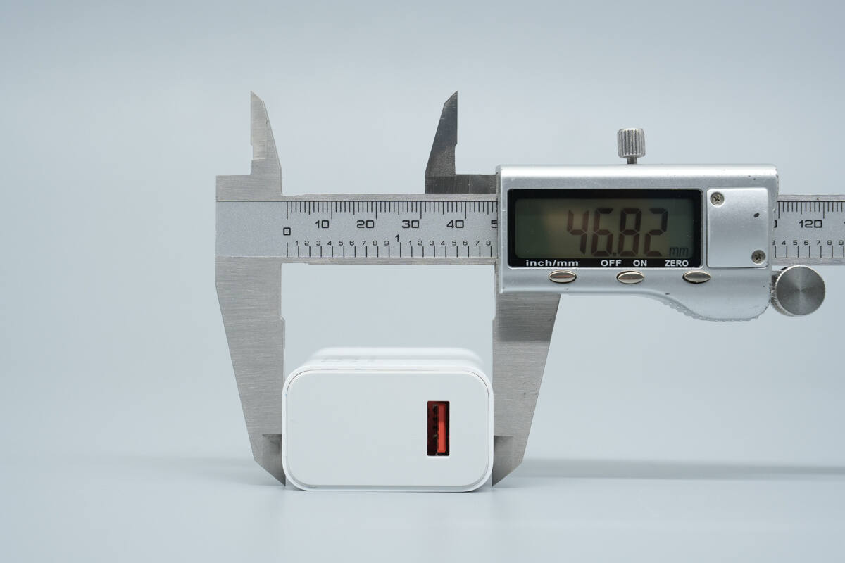
The thickness is about 46.82 mm (1.84 inches).
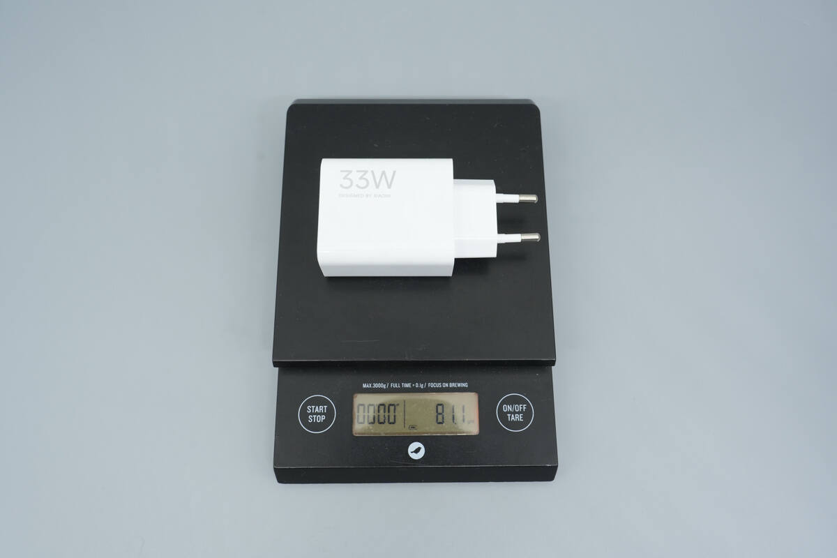
The weight is about 81.1 g (2.86 oz).
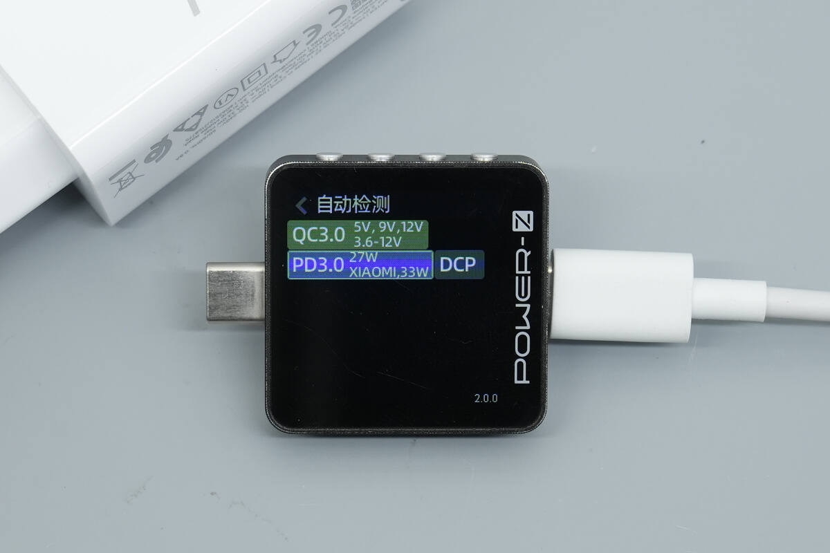
ChargerLAB POWER-Z KM003C shows that the USB-A port supports QC3.0, PD3.0, Xiaomi’s proprietary fast-charging protocol, and the DCP protocol.
Teardown
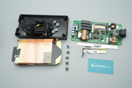
Next, let's take it apart to see its internal components and structure.
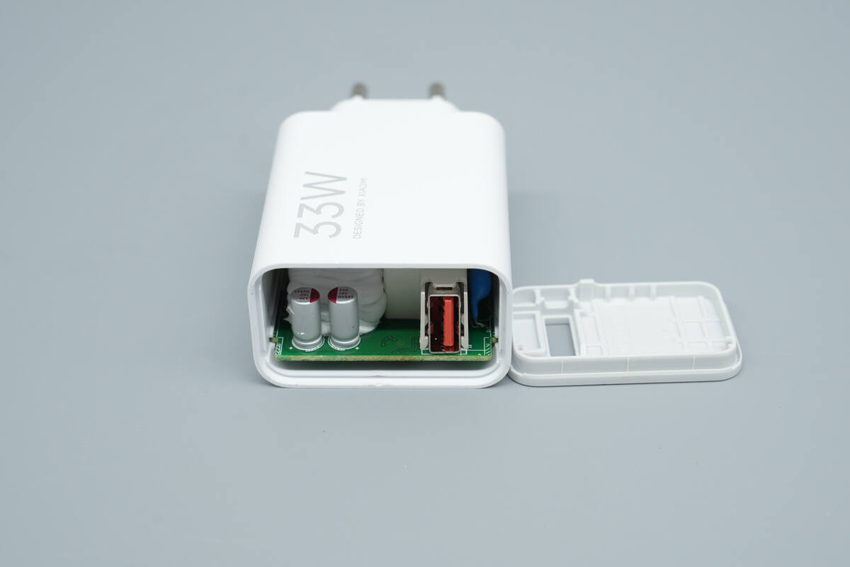
Pry open the housing along the seam at the bottom edge.
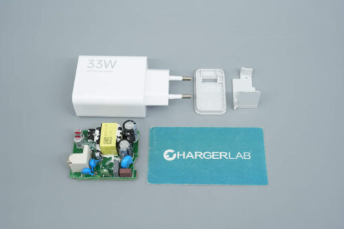
The PCBA module is removed. The component layout is highly compact.
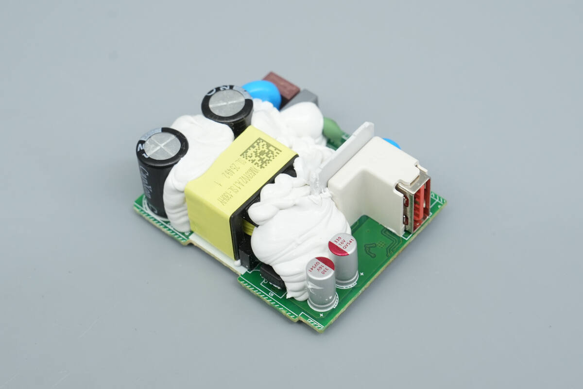
Front view of the PCBA module.
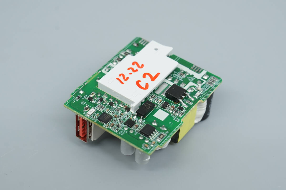
The rear side of the PCBA module is covered with a white plastic insulating plate.
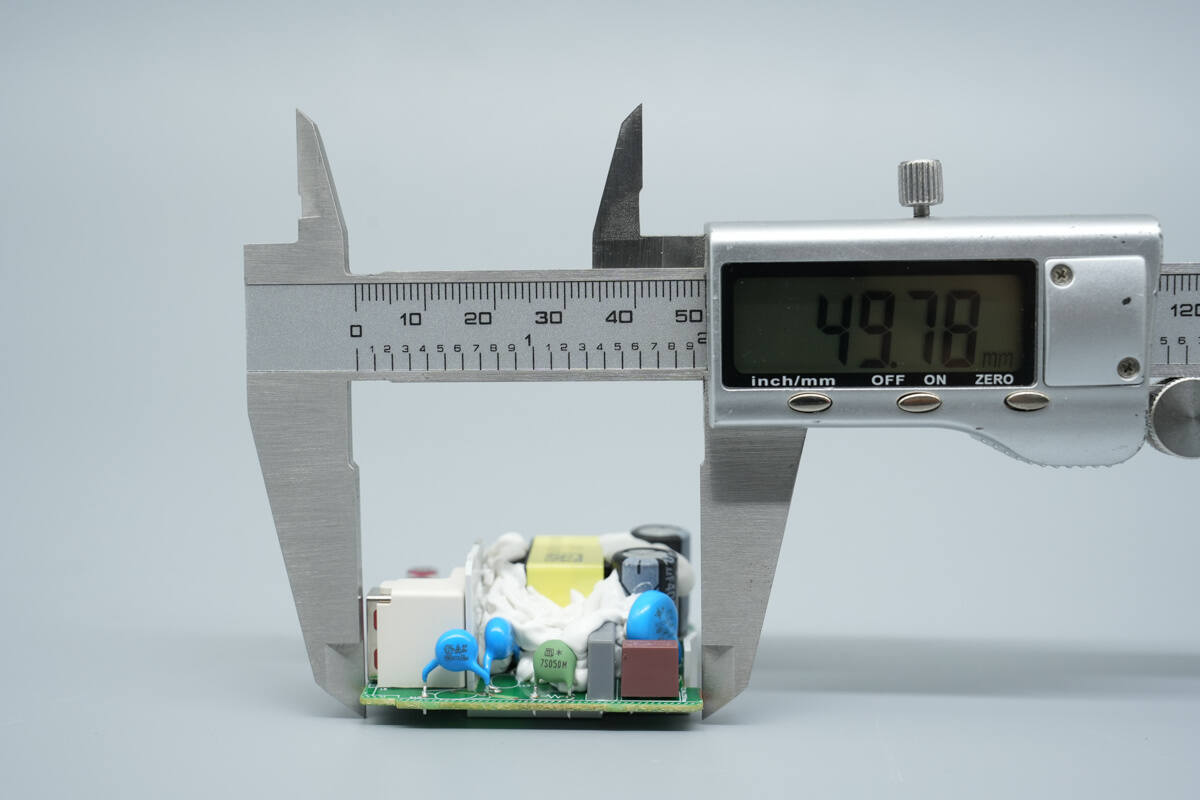
The length of the PCBA module is about 49.78 mm (1.96 inches).
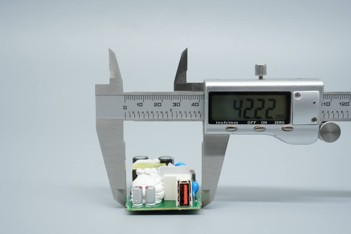
The width is about 42.22 mm (1.66 inches).
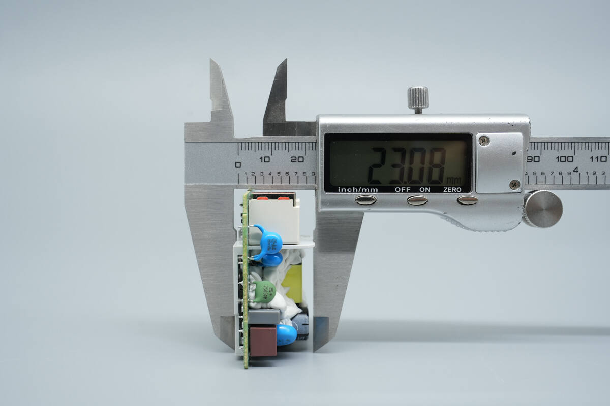
The thickness is about 23.08 mm (0.91 inches).
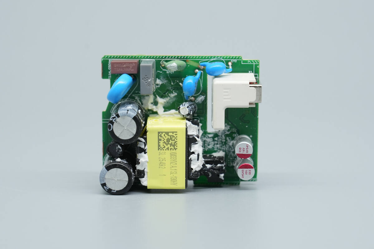
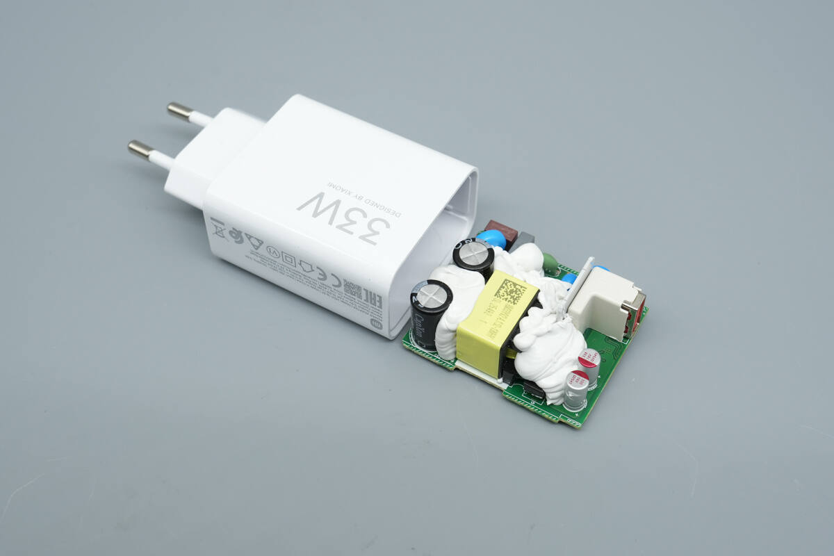
After removing the potting compound, the boundary between the primary high-voltage side and the secondary low-voltage side of the PCBA becomes clearly visible.
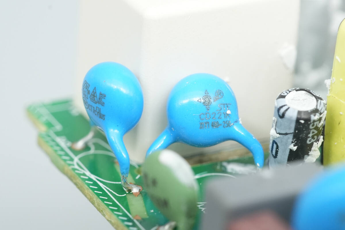
Two blue Y capacitors are placed at the input stage, one of which is from STE. They are used to suppress high-frequency common-mode noise generated by the switching power supply.
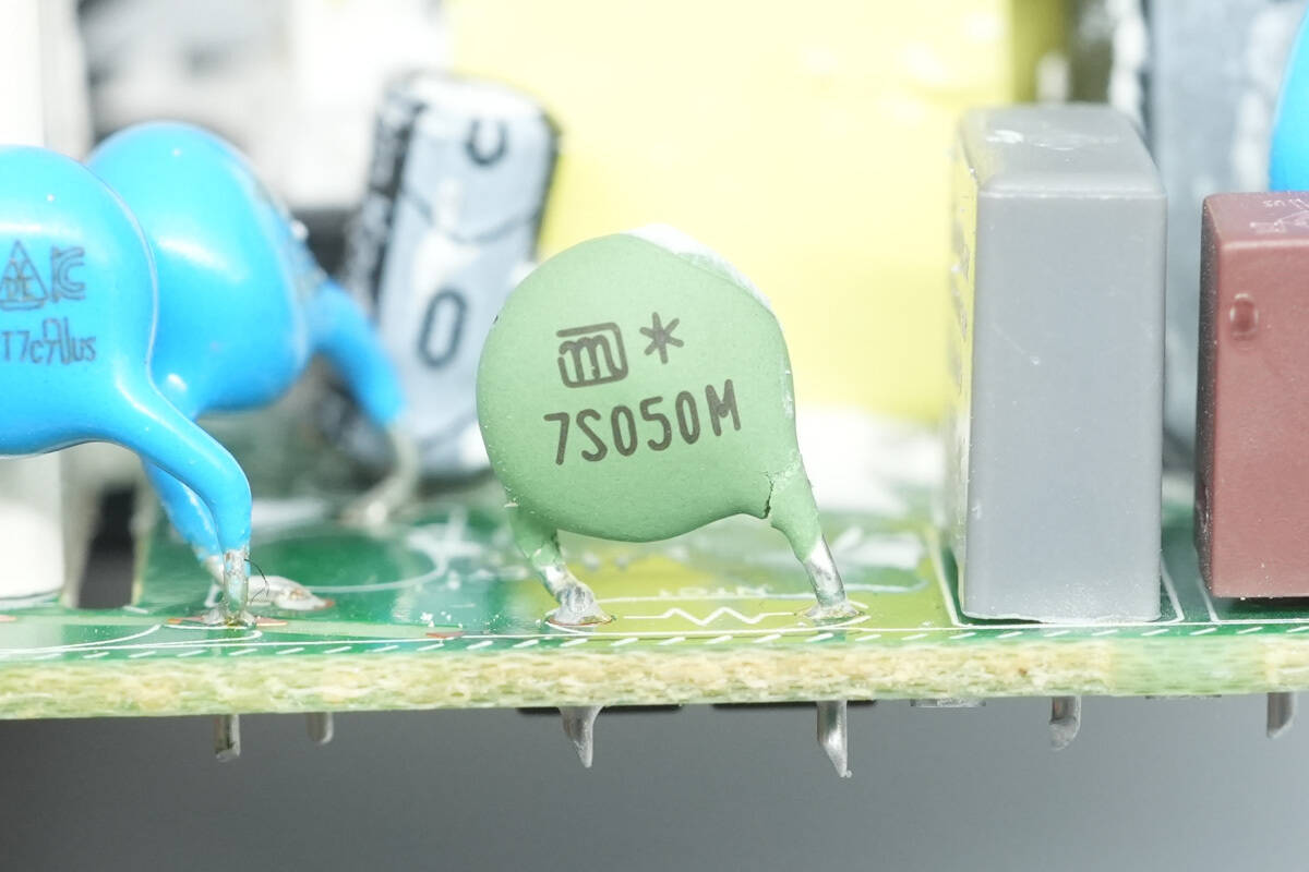
The green NTC thermistor is marked “7S050M”.
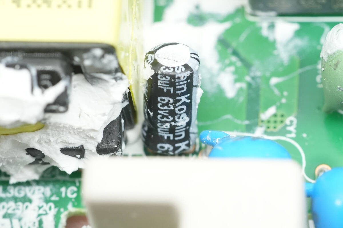
The electrolytic capacitor supplying power to the primary controller is from Koshin, rated at 3.3μF 63V.
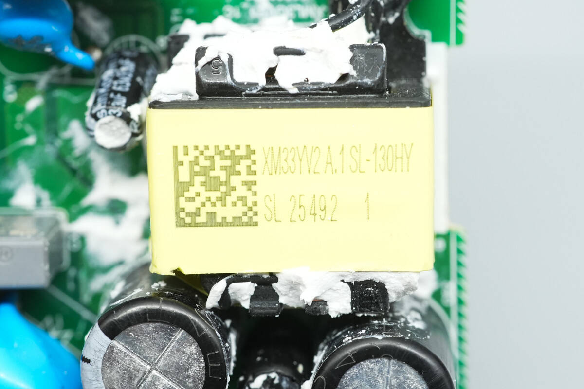
The transformer is marked with XM33YV2A.1SL-130HY.
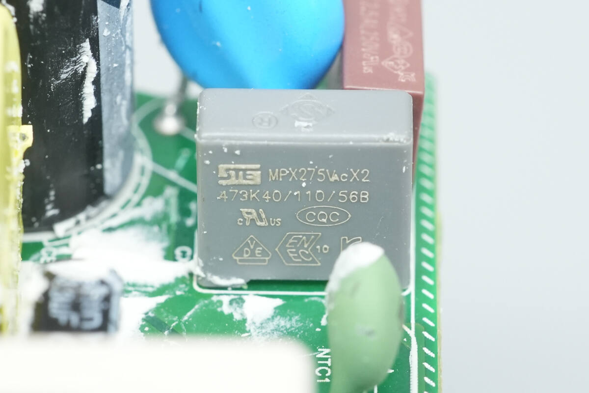
The safety-certified X2 capacitor is from STE, rated at 0.47μF (473K), and is used for differential-mode noise suppression.
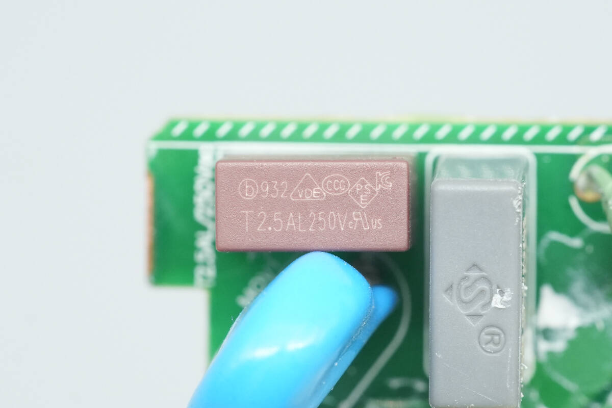
The time-delay fuse, specification T2.5AL250V.
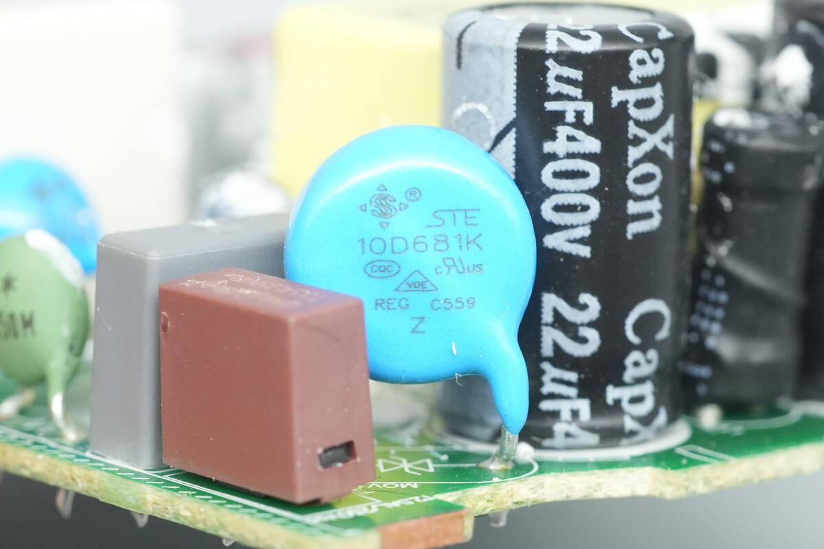
The varistor is from STE, marked “10D681K”, and is used for surge and lightning protection.
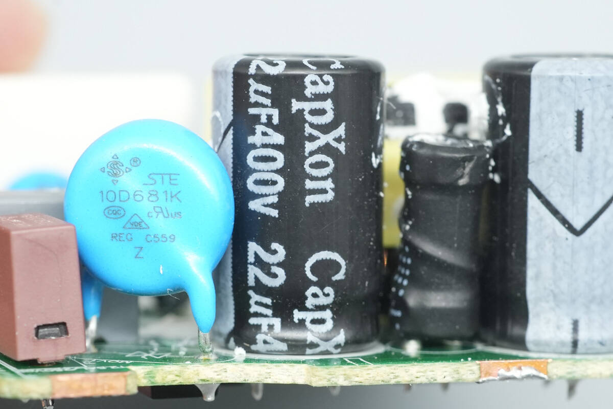
This high-voltage filter electrolytic capacitor is from CapXon, rated at 22μF 400V.
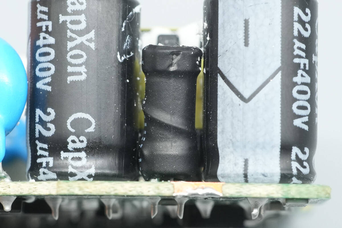
The I-shaped inductor is positioned between the two high-voltage electrolytic capacitors and is covered with black heat-shrink tubing for insulation protection.
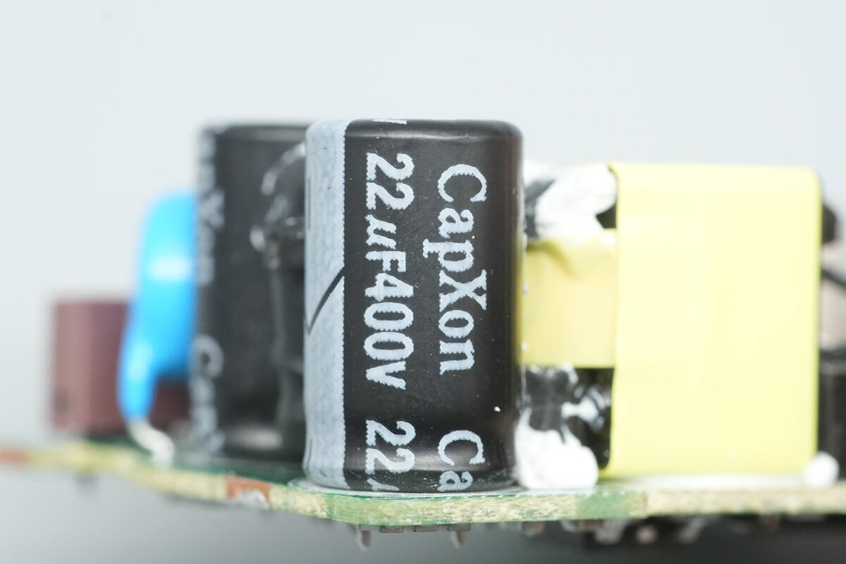
The second high-voltage filter electrolytic capacitor is also from CapXon, rated at 22μF 400V.
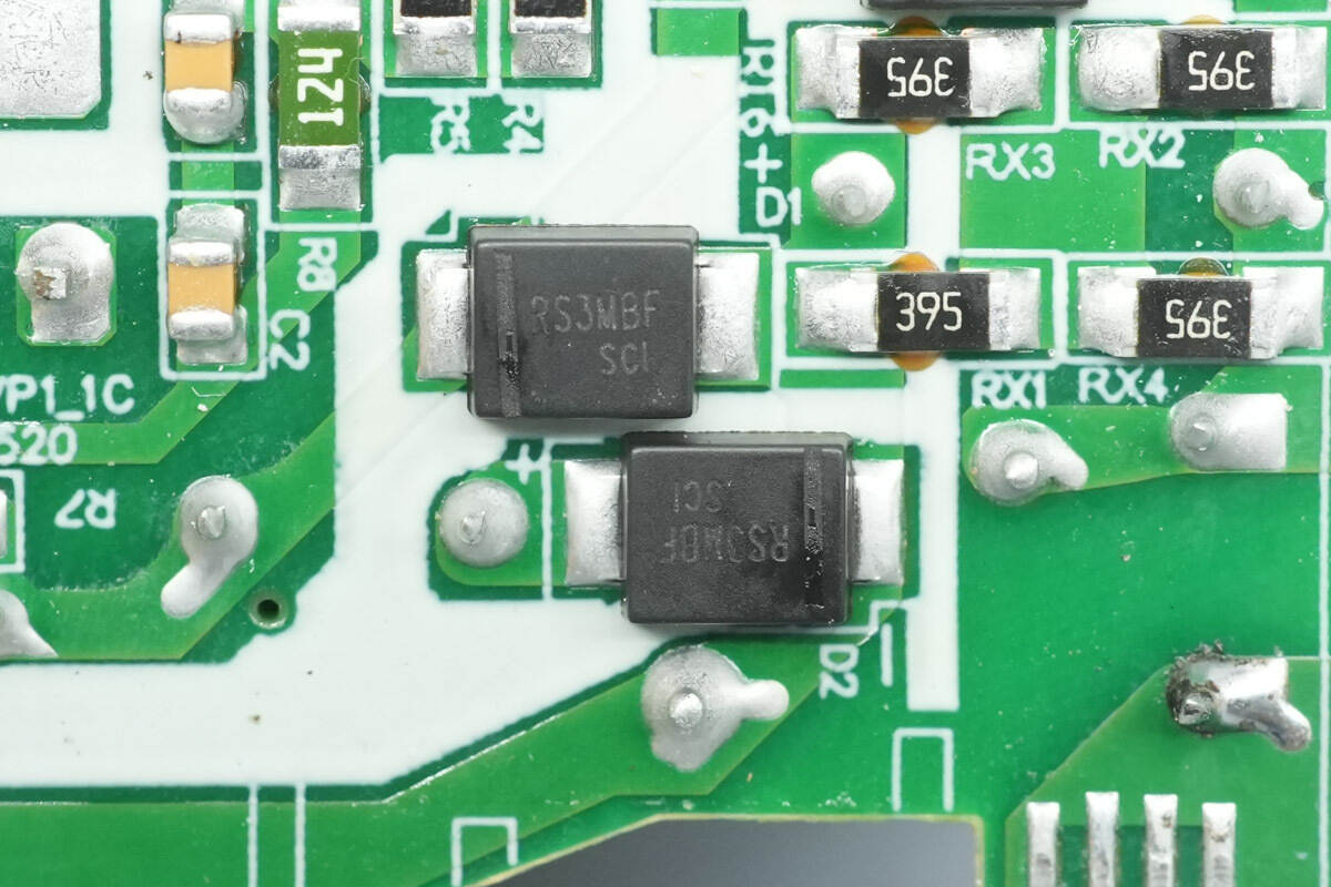
Diodes marked “RS3MBF” form a bridge rectifier circuit.
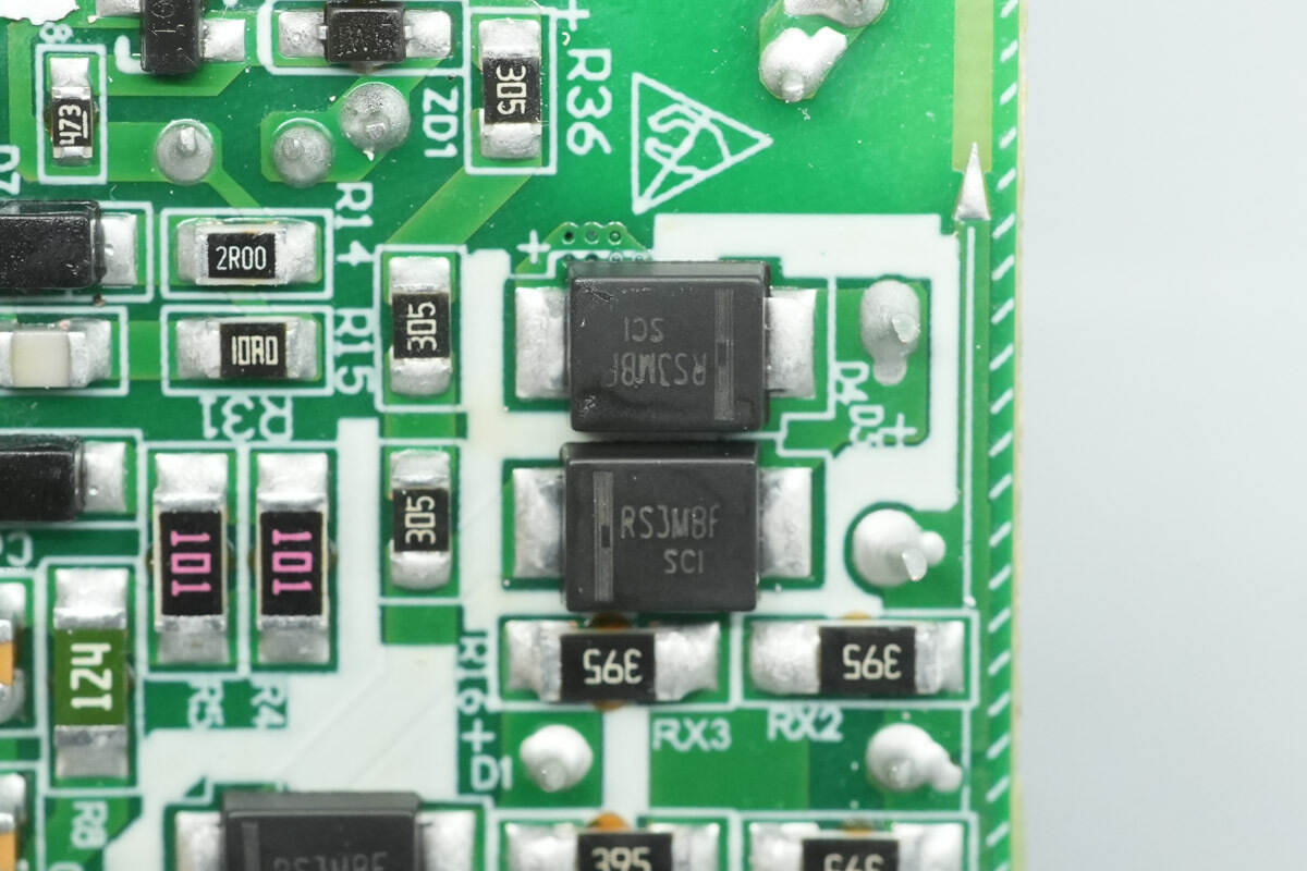
Close-up of the other two diodes marked “RS3MBF”.
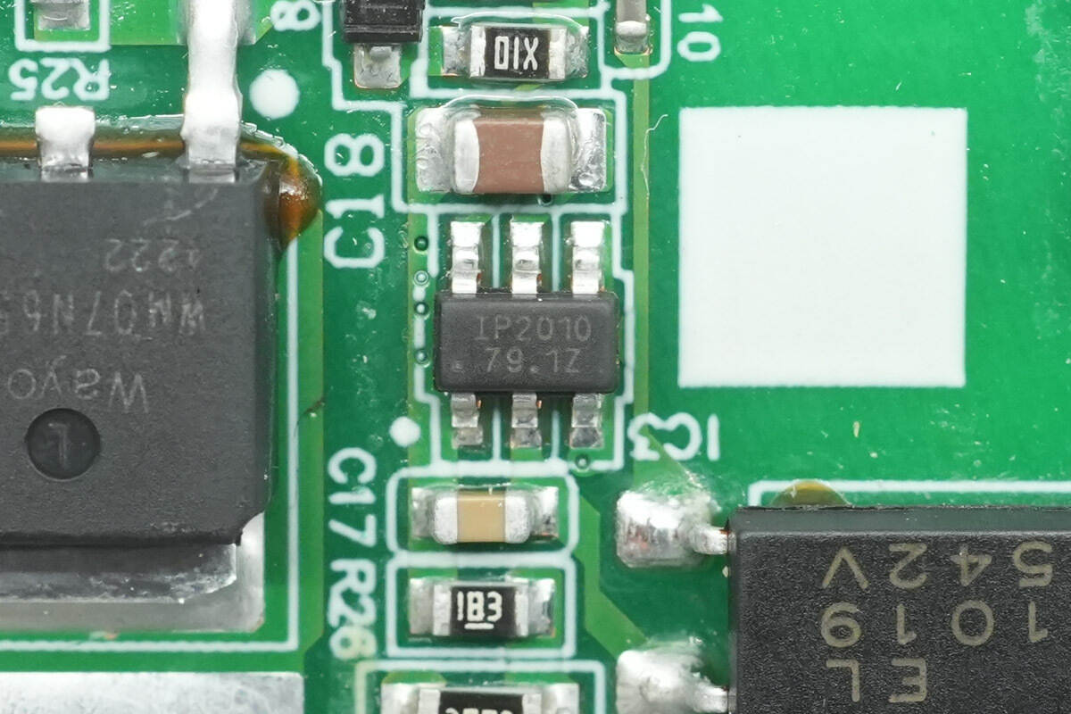
The Injoinic IP2010 is an offline AC/DC primary-side flyback controller in an SOT23-6 package. It adopts an adaptive multi-mode control scheme with secondary-side regulation. By combining frequency foldback with valley switching, it effectively reduces switching losses, enabling high conversion efficiency across a wide range of input and output conditions.
In addition, the built-in frequency jittering function significantly reduces EMI emissions and common-mode noise, helping to optimize transformer design and simplify overall EMC compliance of the power supply.
When operating under light-load or no-load conditions, the IP2010 automatically enters burst mode, with a quiescent current as low as 250 µA, significantly reducing standby power consumption. This allows the system to fully comply with stringent international energy efficiency standards such as CoC V5 and DoE Level VI.
In addition, the device integrates a comprehensive set of configurable protection features, including brown-in/brown-out protection, multiple over-voltage protections, over-temperature protection, as well as accurate constant-current and over-power protection with input-voltage compensation.
These characteristics make it well-suited for applications such as smartphone and laptop adapters, high-power fast chargers, and efficient flyback-based auxiliary power supplies.
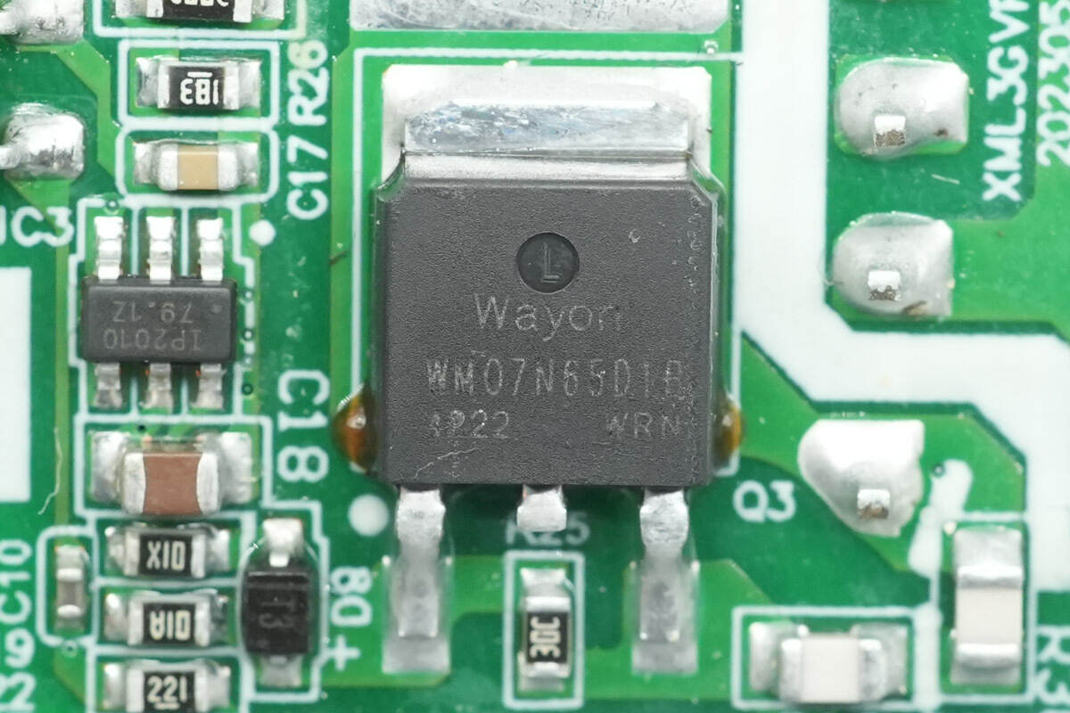
The primary-side MOSFET is from Wayon, marked “WM07N65D1B”, and is a 650V-rated planar MOSFET.
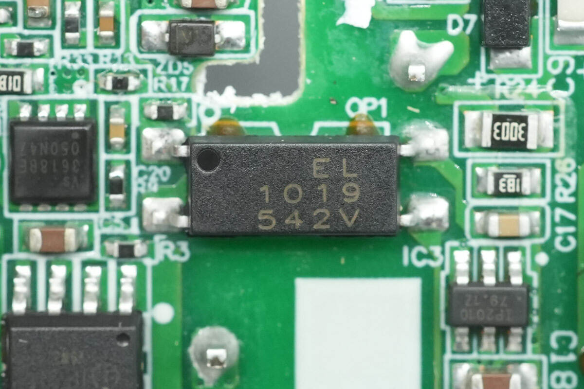
The optocoupler is marked “EL1019” and is used for precise output voltage feedback regulation.
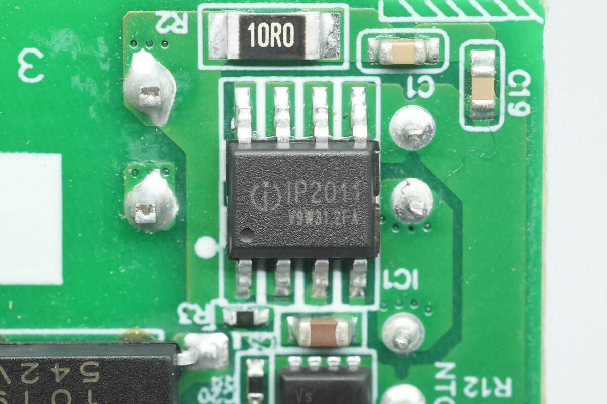
The synchronous rectifier controller is from Injoinic, model IP2011, in an SOP8L package. It is a synchronous rectification controller with an integrated 65V / 8mΩ MOSFET, specifically designed for secondary-side rectification in flyback switching power supplies.
The IP2011 supports continuous conduction mode (CCM), discontinuous conduction mode (DCM), and quasi-resonant operation, and is compatible with both high-side and low-side rectification configurations. It features an internal regulation circuit and can operate stably across a wide output voltage range of 3.3V to 12V without requiring an external auxiliary winding for power supply.
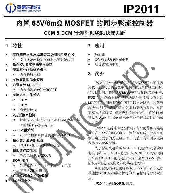
The external circuitry of the IP2011 is highly simplified, requiring only a single capacitor and a single resistor to achieve full functionality. This significantly reduces PCB footprint and BOM cost, making it well-suited for power adapters, PD/QC fast chargers, and flyback-based auxiliary power systems.
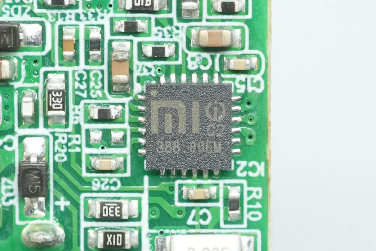
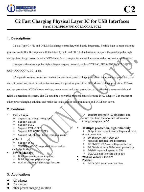
The Injoinic C2 is a highly integrated fast-charging protocol controller chip specifically customized for Xiaomi, packaged in QFN24. It natively supports Xiaomi’s proprietary fast-charging protocol, and while meeting customized requirements, it also maintains broad compatibility and versatility. The chip supports multiple fast-charging standards, including USB PD 3.0 with PPS, QC 4+, UFCS (Universal Fast Charging Specification), and BC1.2.
The chip also supports VCONN power delivery and SOP communication for e-marker cables. It is primarily designed for applications such as power adapters, car chargers, and smart power strips, providing a highly integrated physical-layer solution for USB Type-C interfaces.
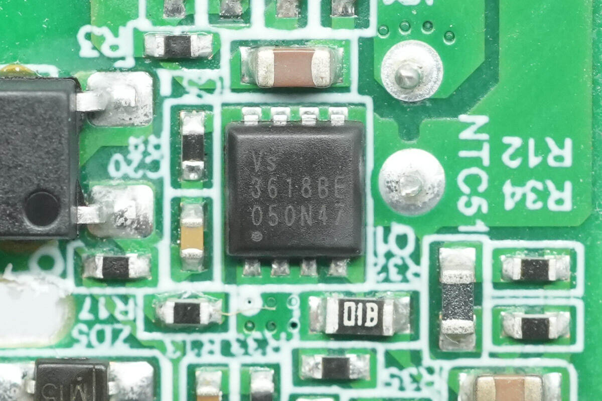
The VBUS MOSFET is from Vergiga, model VS3618BE. It is an N-channel MOSFET rated at 30V with an on-resistance of 5.2mΩ, and comes in a PDFN3333 package.
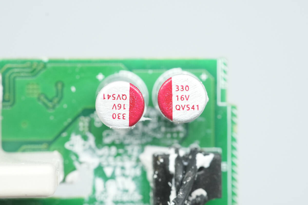
The output filtering capacitors are rated at 16V 330μF.

Well, those are all components of the Xiaomi 33W USB-A Charger.
Summary of ChargerLAB
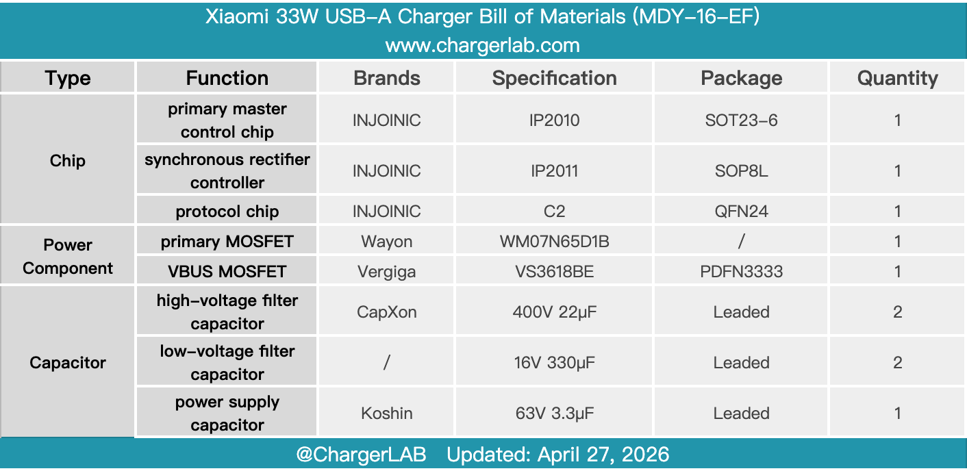
Here is the component list of the Xiaomi 33W USB-A Charger for your convenience.
It supports Xiaomi’s 33W proprietary fast-charging protocol, and is also compatible with QC 3.0 as well as PD protocols up to 27W, delivering a solid fast-charging experience across mainstream smart devices on the market.
After taking it apart, we found that the PCBA is extensively filled with white potting compound, which significantly improves thermal dissipation and also provides mechanical protection for key components such as the transformer and electrolytic capacitors. The master control chip, synchronous rectification controller, and custom fast-charging protocol chip are all from Injoinic.
This highly integrated chipset solution simplifies the external circuitry design, effectively reducing PCB size and overall BOM cost, while comfortably meeting the customization requirements of leading smartphone brands and supporting large-scale mass production. The design also incorporates high-voltage electrolytic capacitors from CapXon, a primary MOSFET from Wayon, and VBUS MOSFETs from Vergiga. Overall, this is a well-built charger that balances safety, stability, and efficient fast-charging performance.
Related Articles:
1. Teardown of SHARGE HyperTower 170W Power Bank (X6)
2. Teardown of Baseus PicoGo Air Power Bank (E00337)
3. Teardown of UGREEN Nexode Air 45W GaN Charger (X840)