Introduction
NVIDIA’s 2025 release of the DGX Spark portable server marks a shift toward "desktop supercomputing." Weighing just 1.2kg, this all-metal device brings high-end data center power directly to developers.
Equipped with the GB10 Grace Blackwell superchip and 128GB of unified memory, it effortlessly handles massive models like GPT-OSS 120B and Llama 3.1 70B. With its 200Gb/s QSFP interface, users can even link two units to run distributed inference for 405-billion-parameter models.
ChargerLAB previously put this powerhouse through our rigorous testing process.
To pack the immense power of the GB10 Grace Blackwell superchip into a small frame, NVIDIA externalized the power supply for the DGX Spark, freeing up vital internal space for advanced cooling.
This design choice makes the DGX Spark a pioneer as one of the world's first devices to feature full-spec PD 3.2 240W charging, further accelerating the adoption of USB-C power in the server market.
NVIDIA set exceptionally high standards for this adapter; the 240W unit leverages PD 3.2 and the AVS protocol to handle demanding workloads and instant power surges.
Below, ChargerLAB breaks down the device to reveal its internal engineering and professional-grade components.
Product Appearance
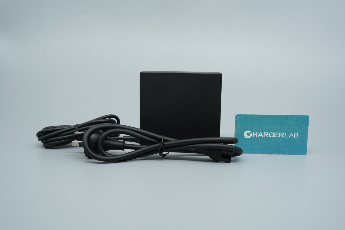
Here is the NVIDIA DGX Spark original 240W power adapter and AC input cable.
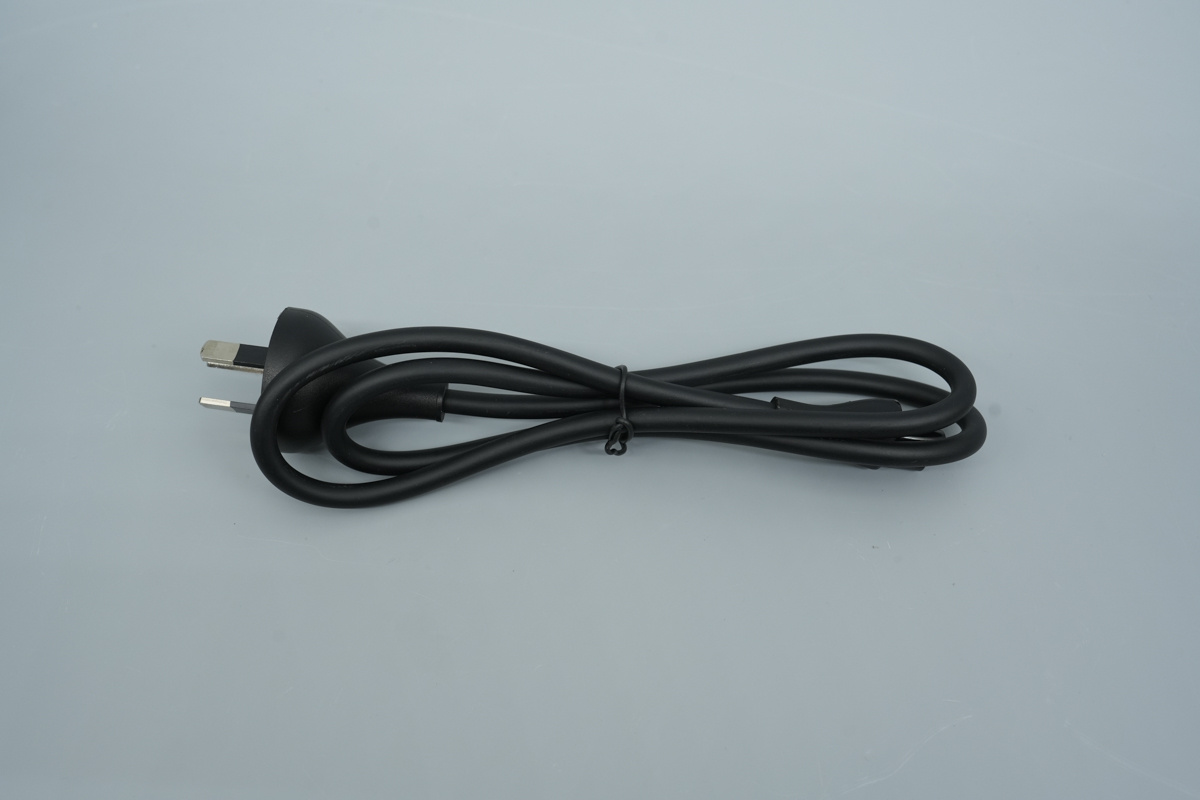
The included AC input cable is of moderate length, flexible material, secured with cable ties for tidy transit.
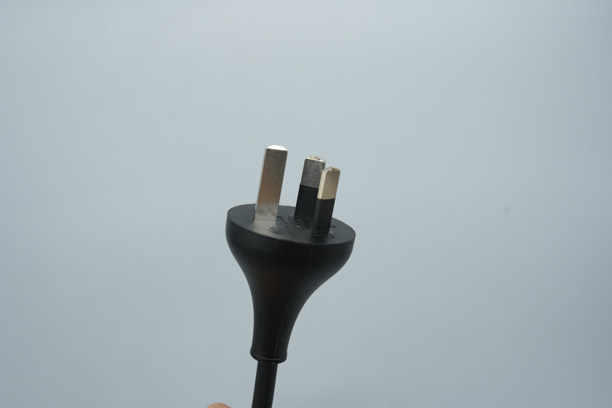
The plug features a standard New Chinese Standard design.
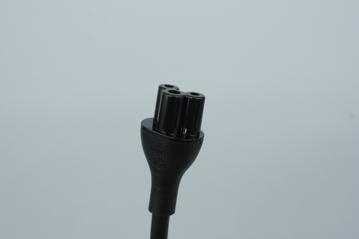
The other end of the power cable is a standard C5 connector, which is well-made and and a satisfyingly smooth tactile feel during use.
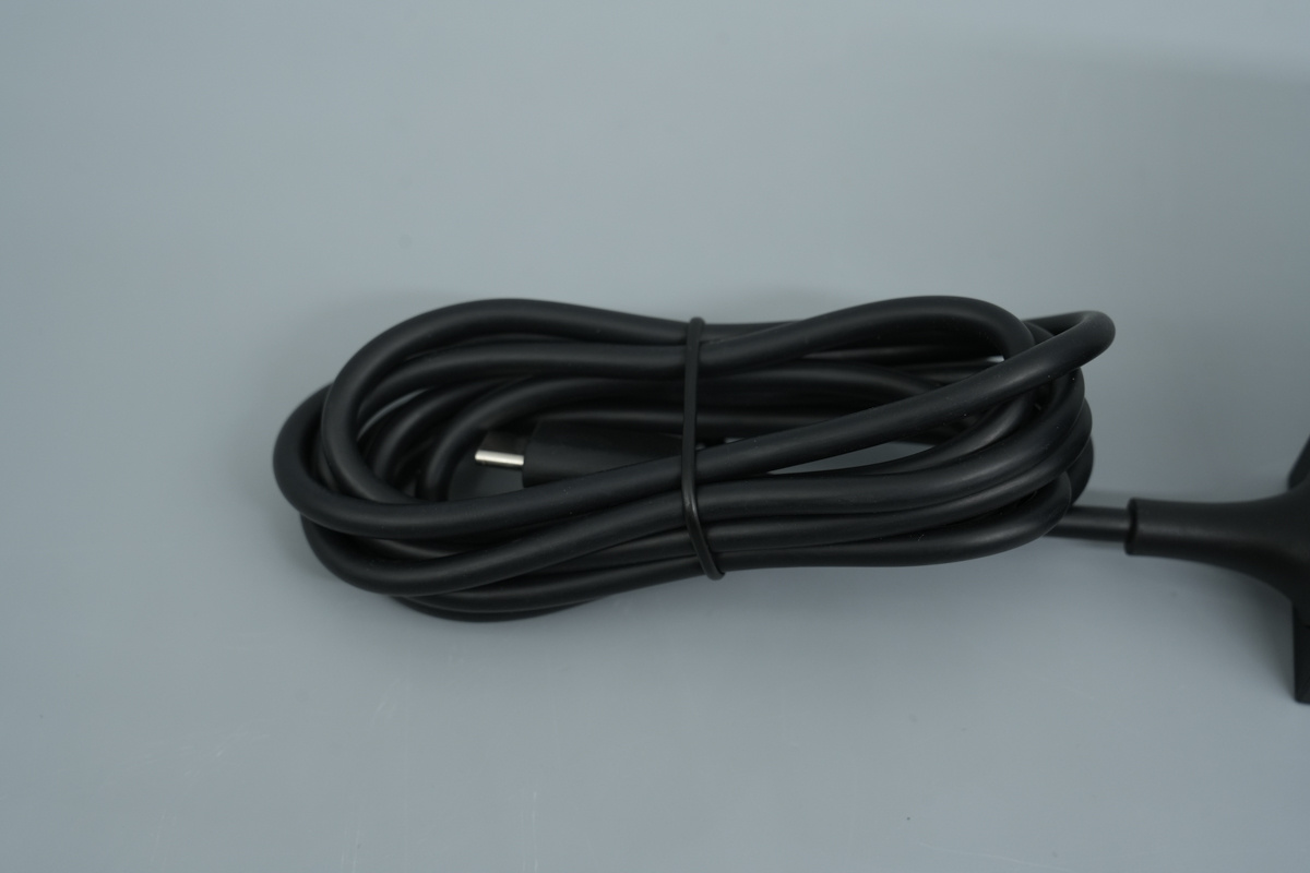
The unit is equipped with an integrated Type-C output cable, which is neatly secured with a bundled cable tie upon delivery.
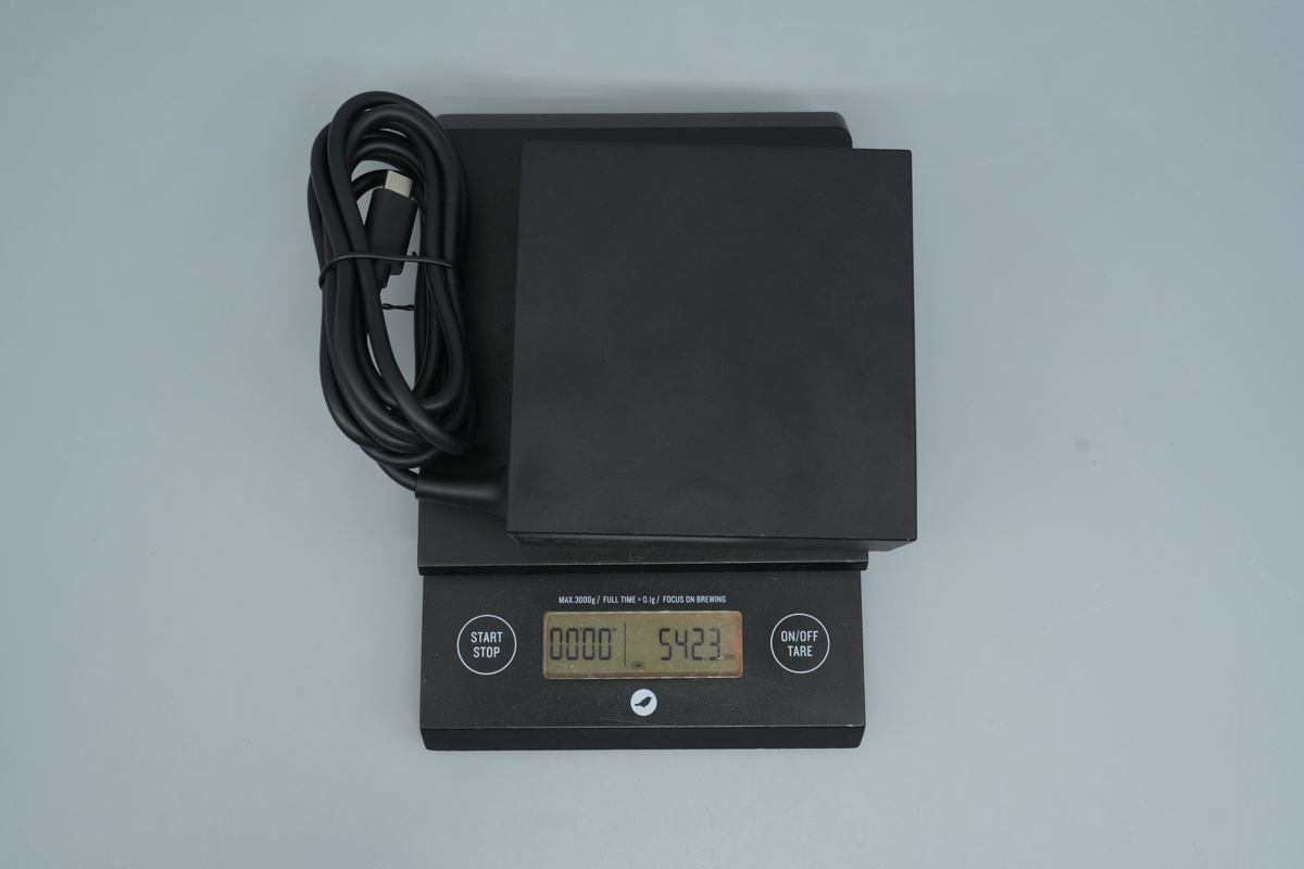
The weight is about 542.3g (19.13 oz).
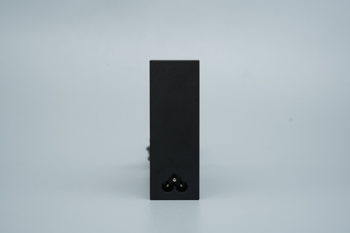
The AC input of it features a recessed C6 connector, providing a secure fit for the matching power cable.
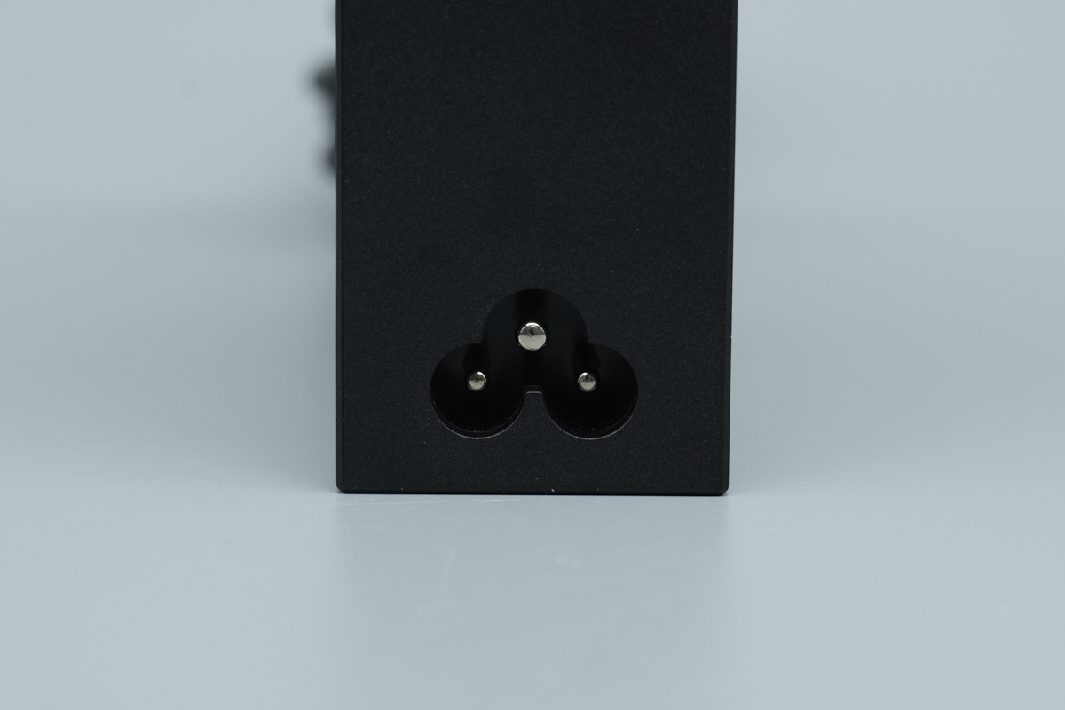
The three pins inside the output interface have a high gloss finish and a large contact area, ensuring stability during high-power input.
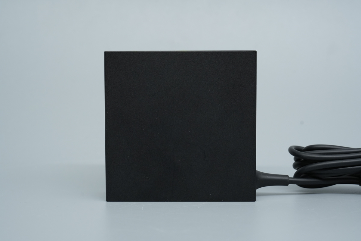
The unit body features a rectangular, matte-black brick design with a fine-textured finish, providing a premium tactile feel while remaining resistant to fingerprints.
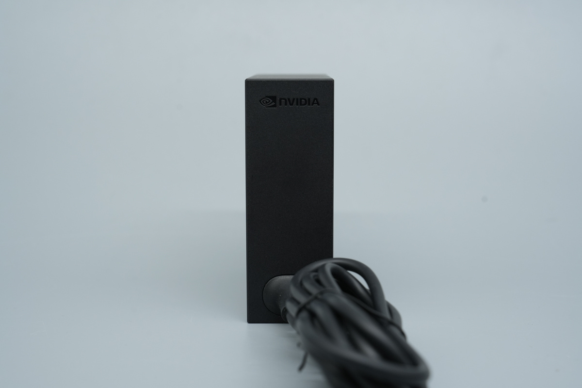
It’s output end is clean and minimalist, highlighted by the NVIDIA logo, while the output cable is neatly integrated at the base.
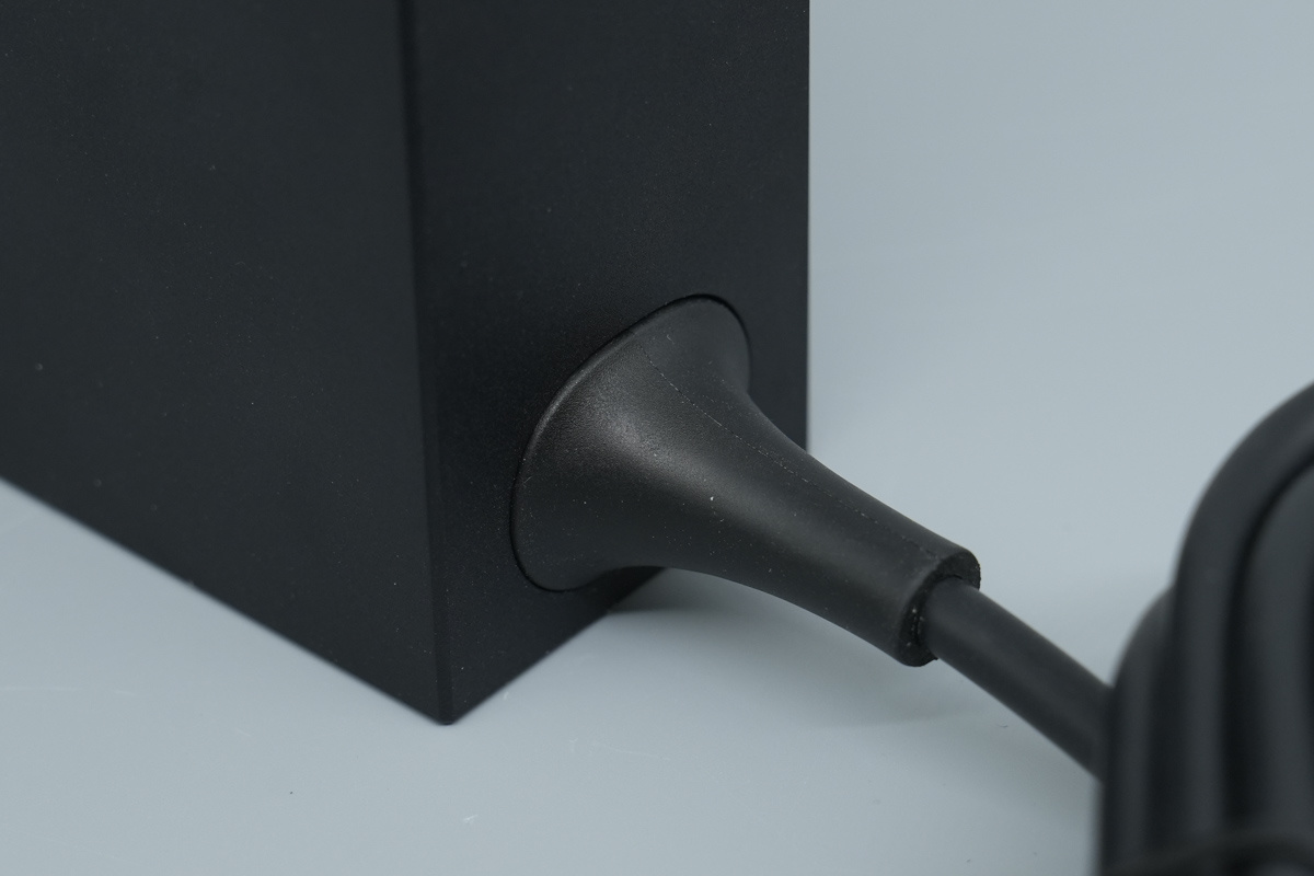
The included Type-C output cable is protected by an extended injection-molded sleeve at the connection point with the device, making it more resistant to bending and pulling.
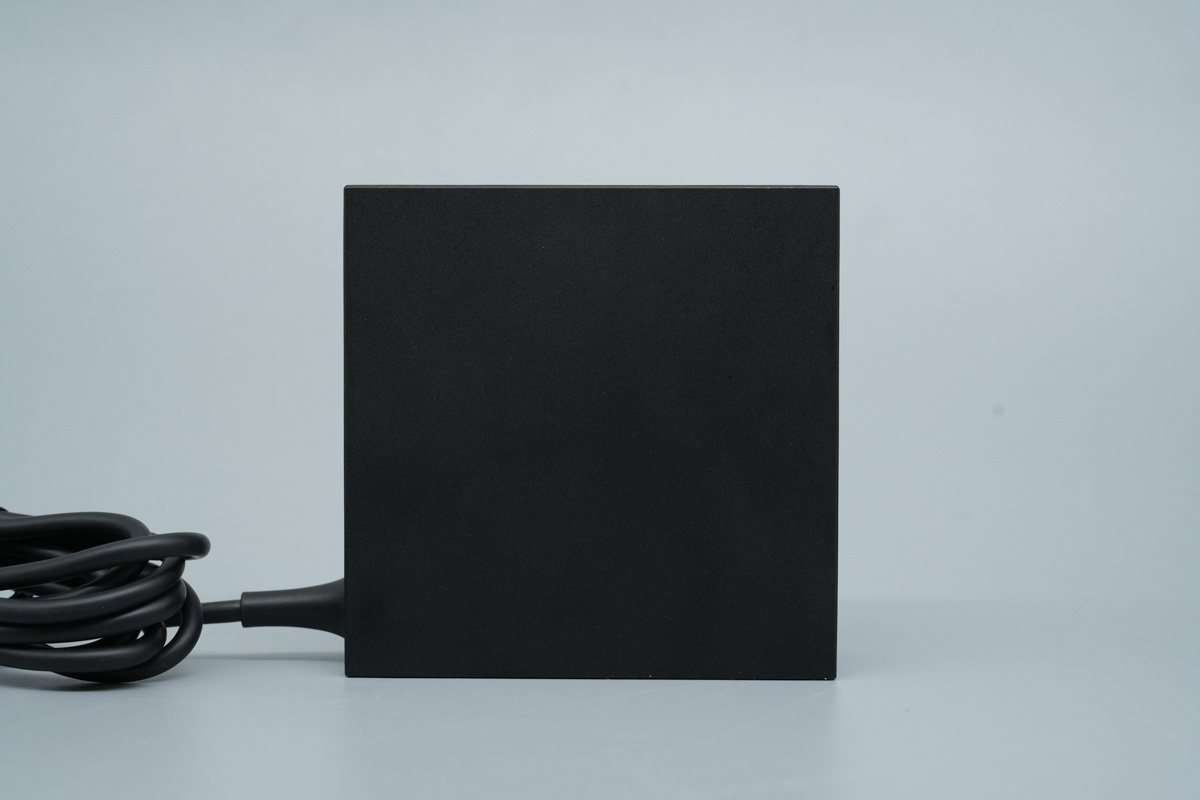
The other side is also minimalist, sleek, and free of extraneous details.
The corners of this unit are relatively sharp, and the edges are all slightly chamfered, resulting in a symmetrical overall visual effect.
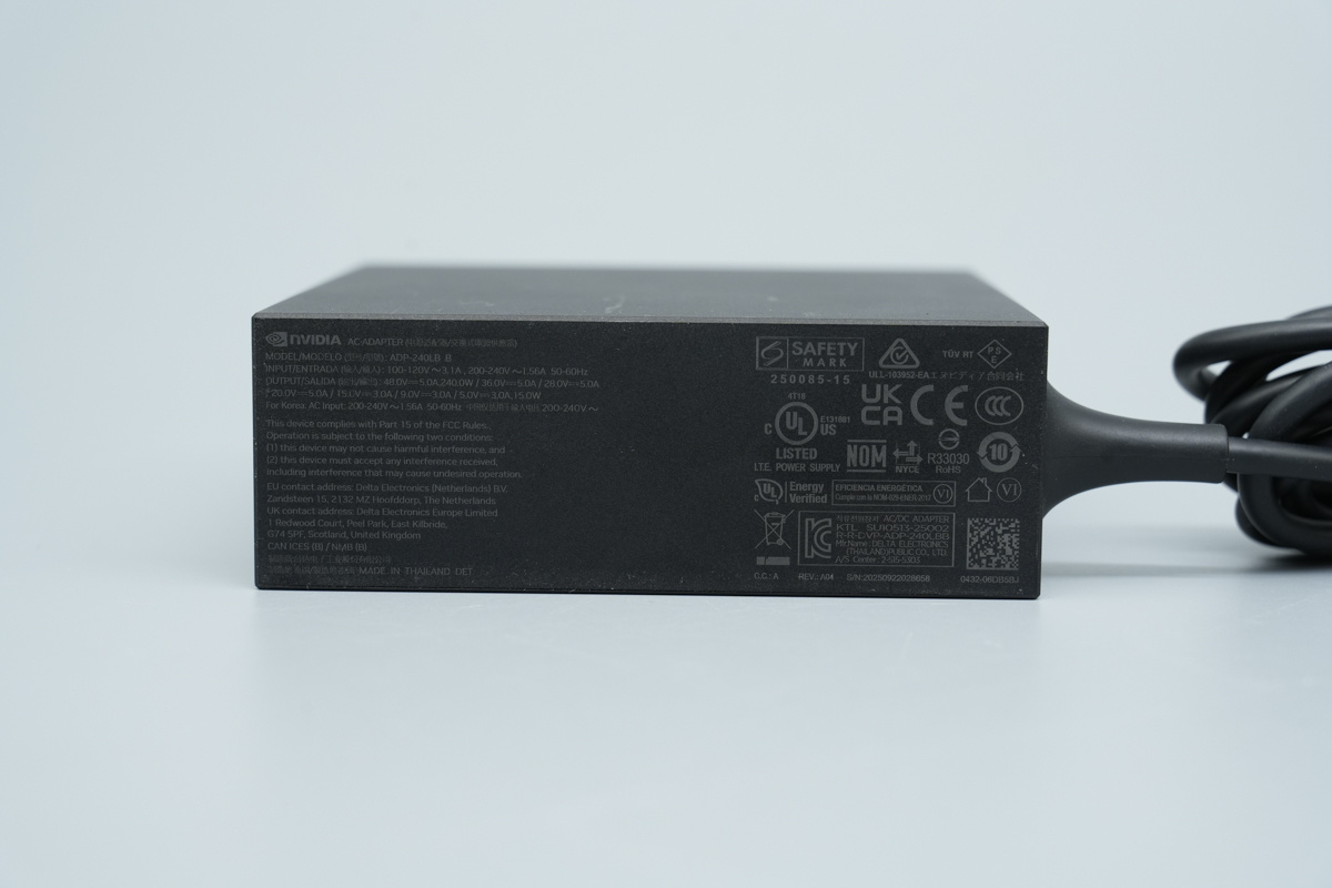
The bottom of it has the product's detailed specs printed on it.
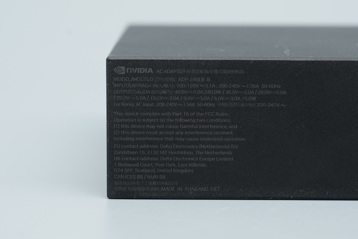
Product Specs:
Model: ADP-240LB B
Input: 100-120V~ 3.1A / 200-240V~ 1.56A, 50-60Hz
Output: 48V/5A, 36V/5A, 28V/5A, 20V/5A, 15V/3A, 9V/3A, 5V/3A
Manufacturer: Delta Electronics, Inc.
Country of Origin: Thailand
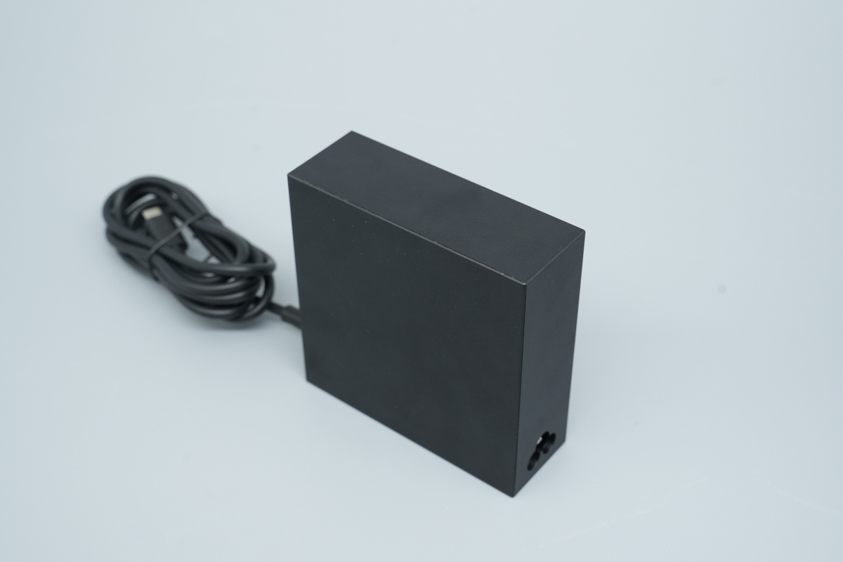
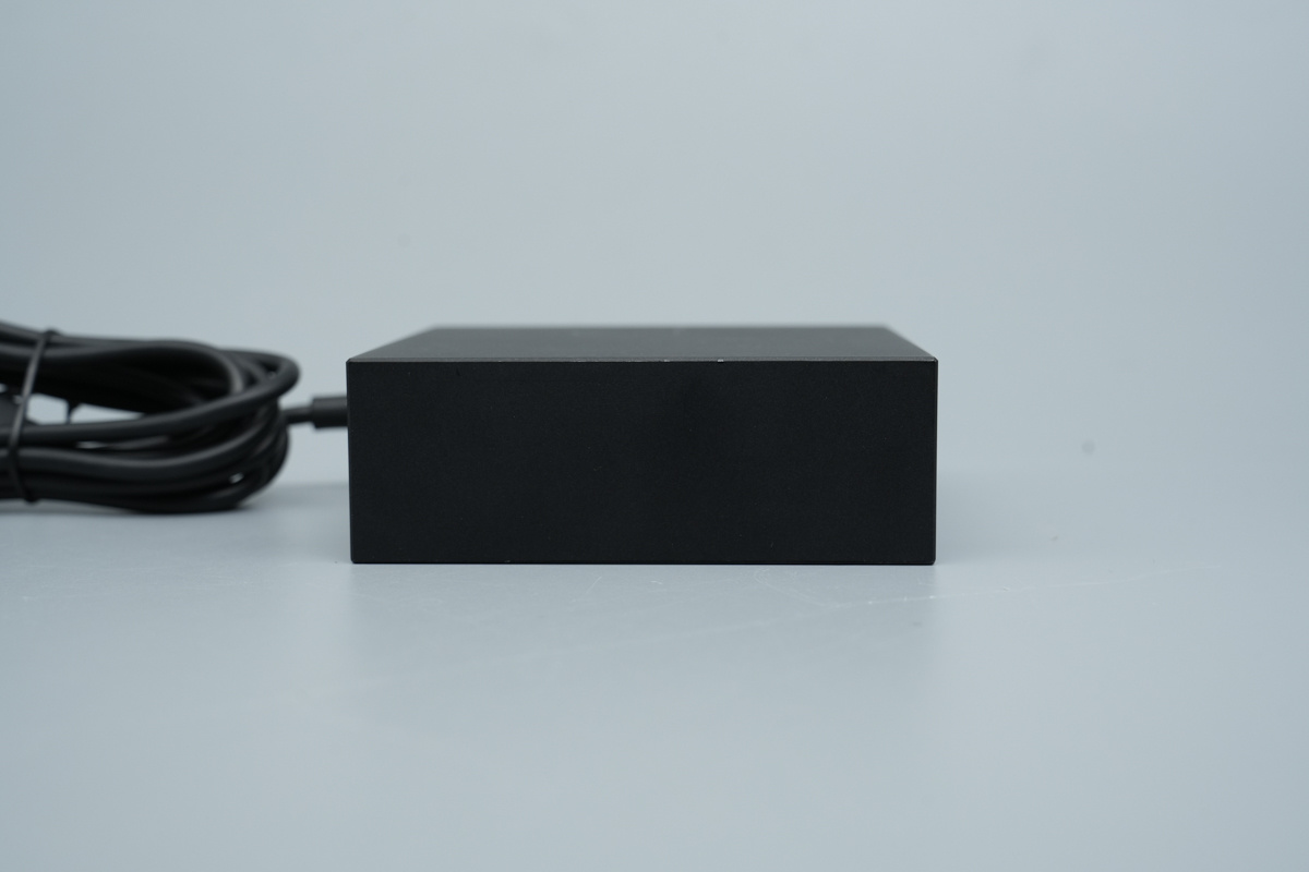
The rigid, rectangular industrial design aesthetic is fully apparent.
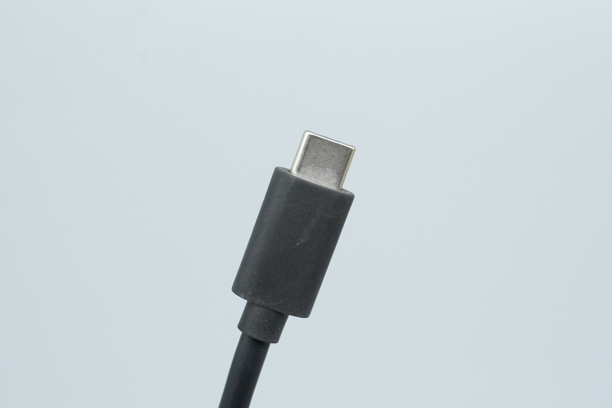
The unit utilizes a USB-C connector for power output.
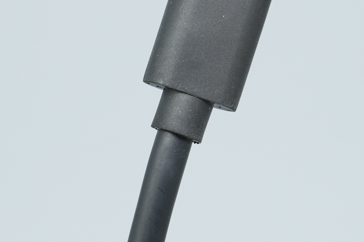
The USB-C connector end includes reinforced strain relief for superior bending and pull resistance.
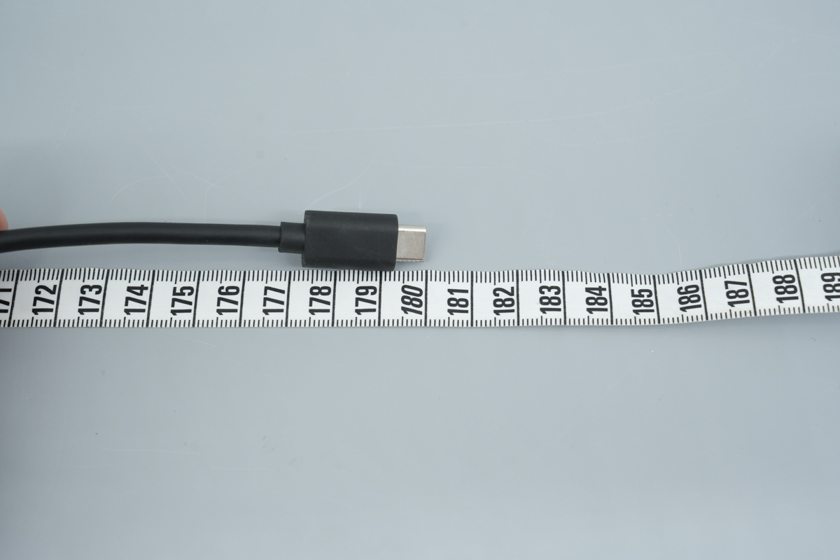
The length of the integrated USB-C output cable is approximately 180cm.
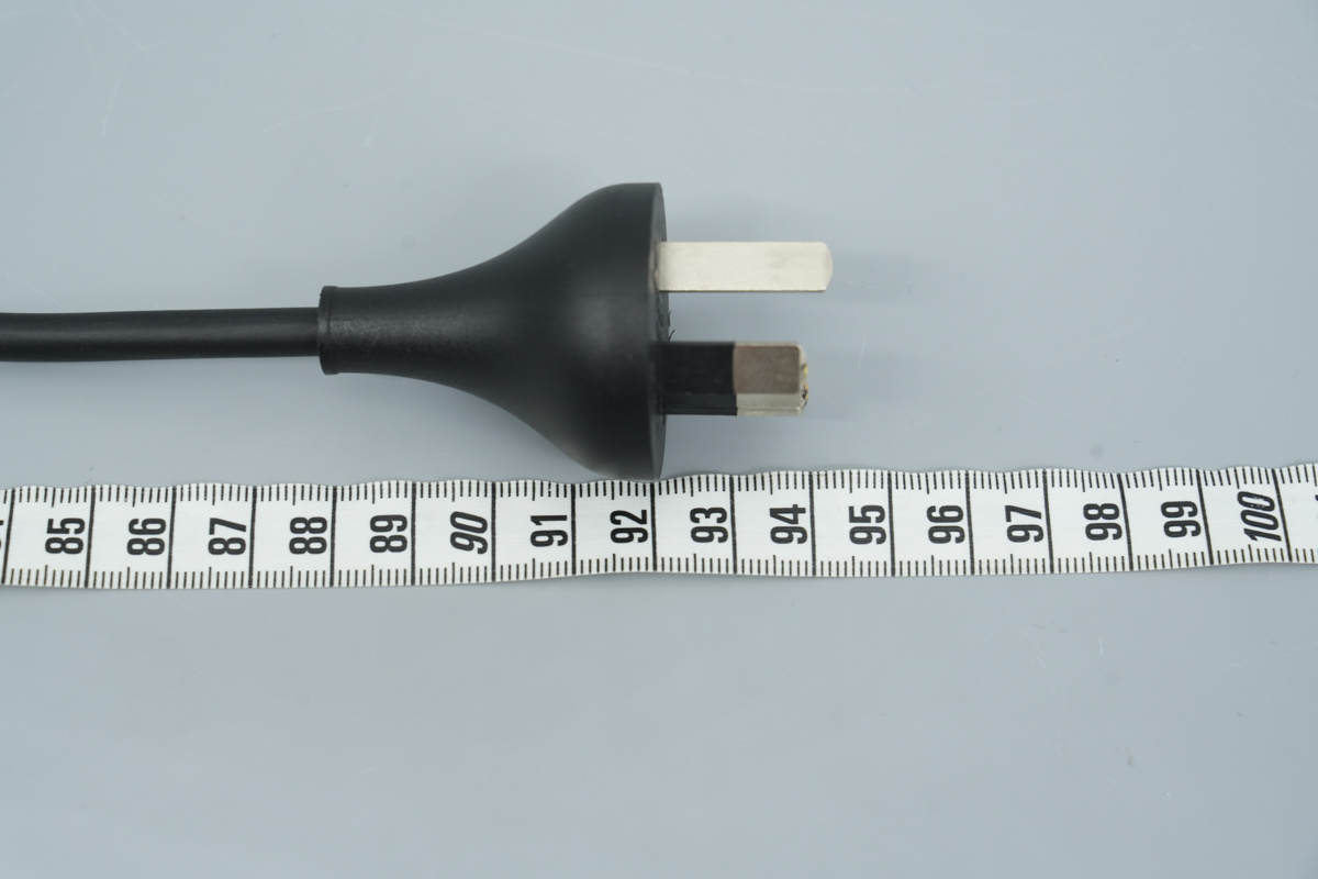
The length of the AC power input cable is approximately 94cm.
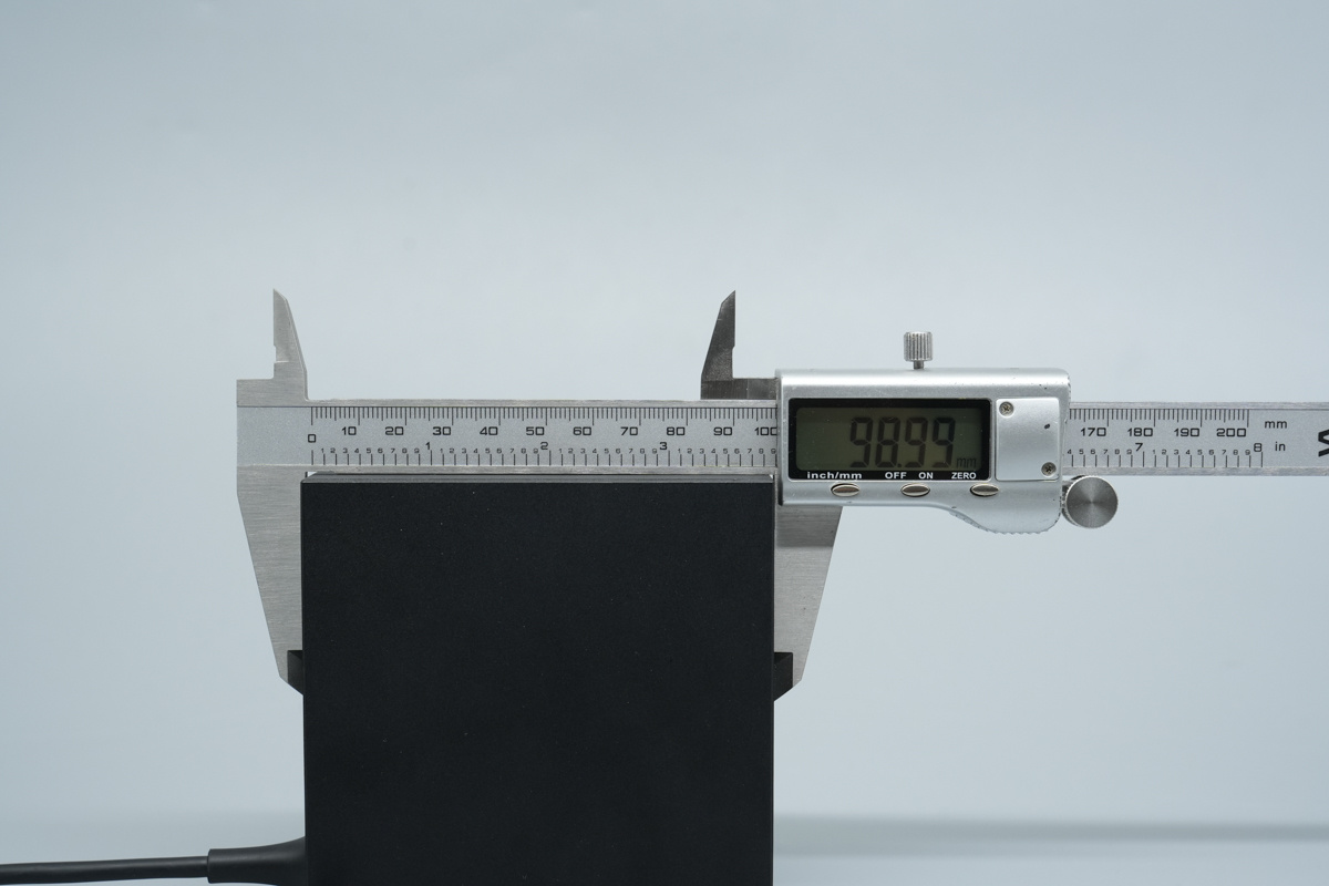
The length of the unit is about 98.99mm (3.897 inches).
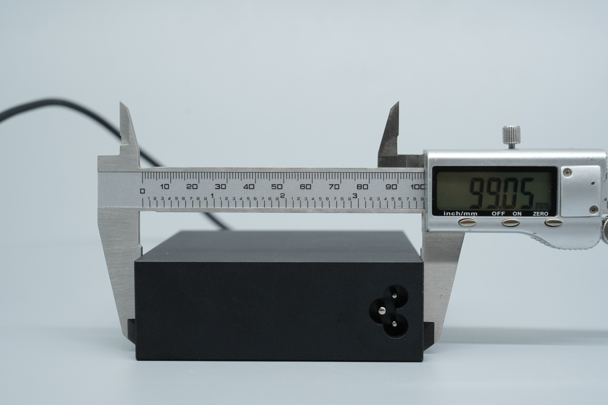
The width of the unit is about 99.05mm (3.900 inches).
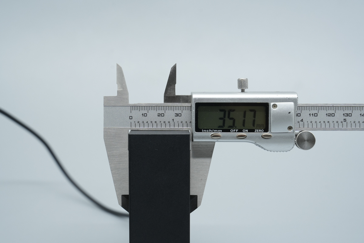
The thickness of the unit is about 35.17mm (1.385 inches).
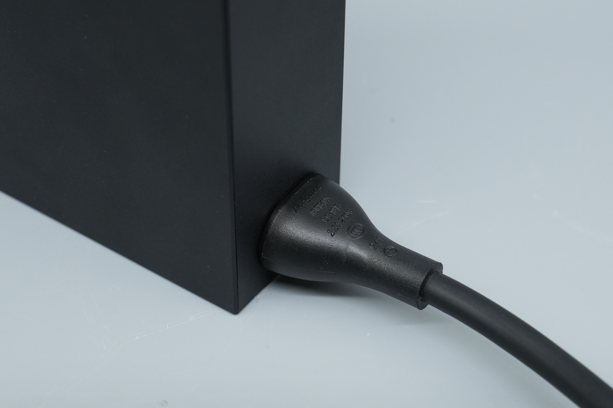
When inserted into the AC input port, the power cable forms a secure, rigid connection with no signs of looseness.
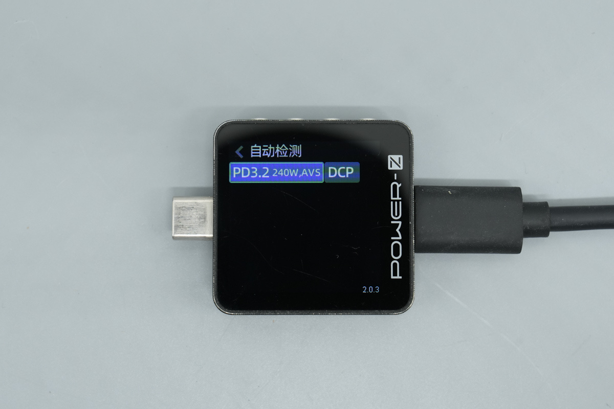
ChargerLAB POWER-Z KM003C shows that the USB-C port supports PD 3.2 240W and AVS.
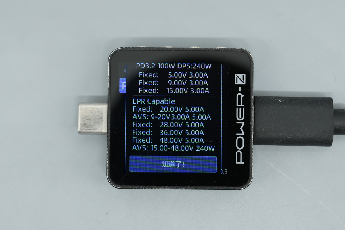
And it also supports seven fixed PDOs of 5V3A, 9V3A, 15V3A, 20V5A, 28V5A, 36V5A and 48V5A, and features AVS subset: 15V-48V 240W.
With the exterior tour and protocol compatibility testing, it's time to dive deeper.
Teardown
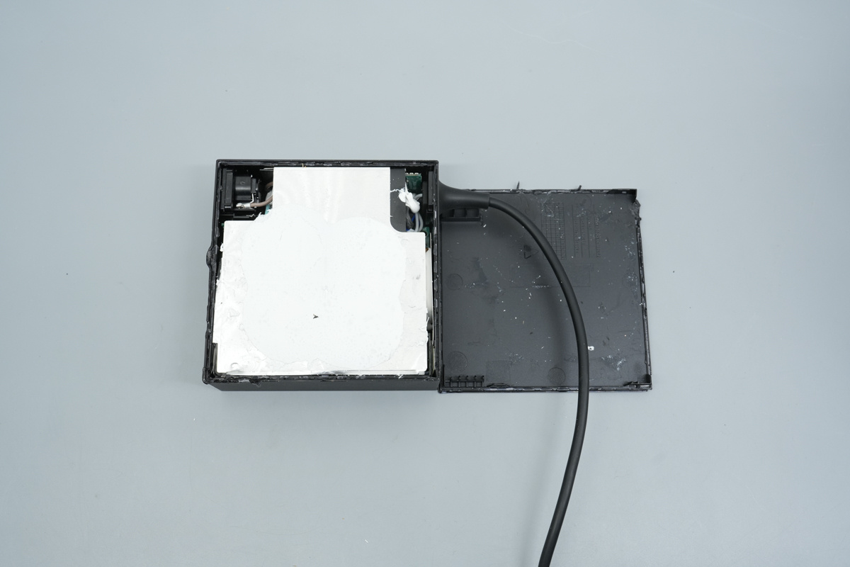
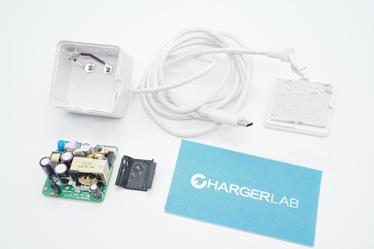
Cutting along the chassis seam and separating the outer casing, the internal PCBA is covered by a robust metal heatsink enclosure.
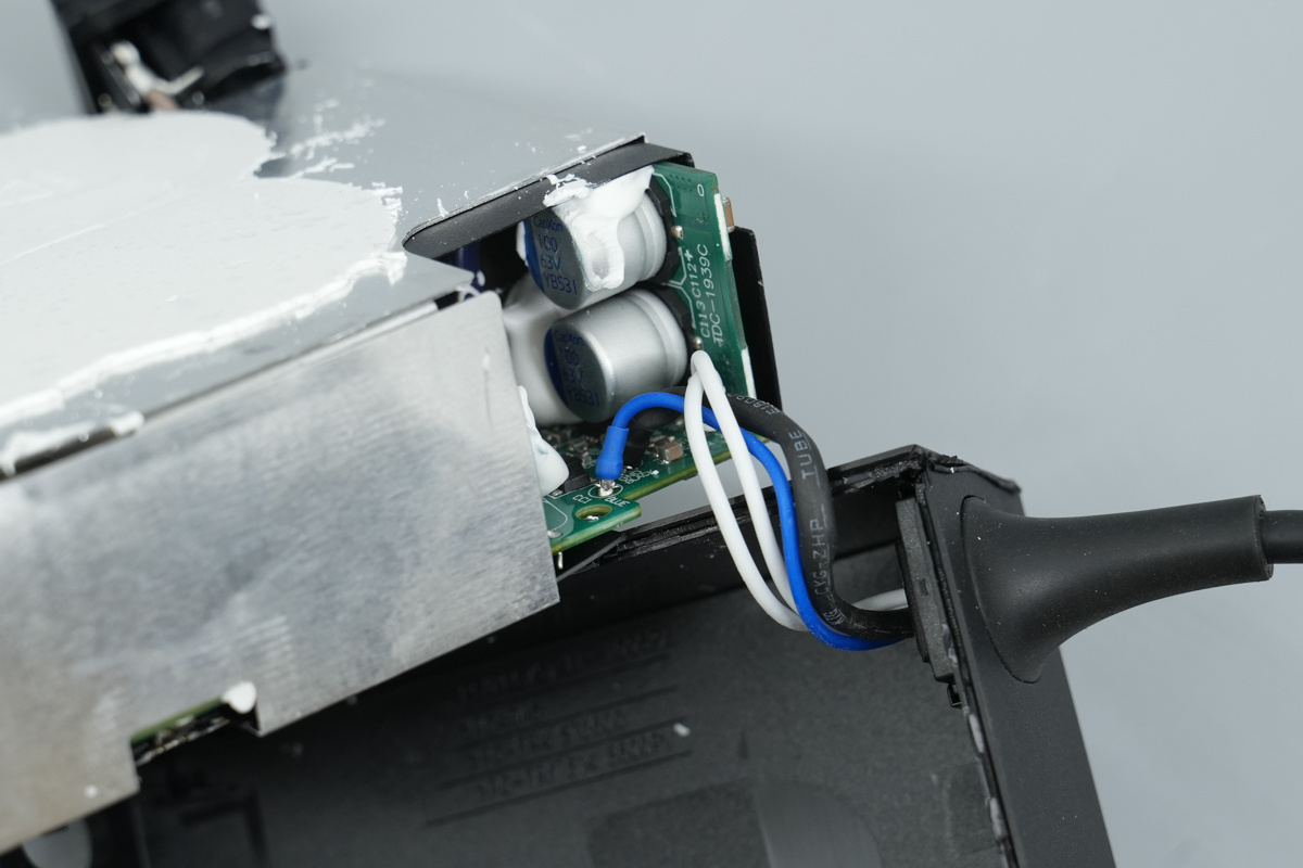
The internal wires of the built-in USB-C cable are connected to the PCBA by soldering.
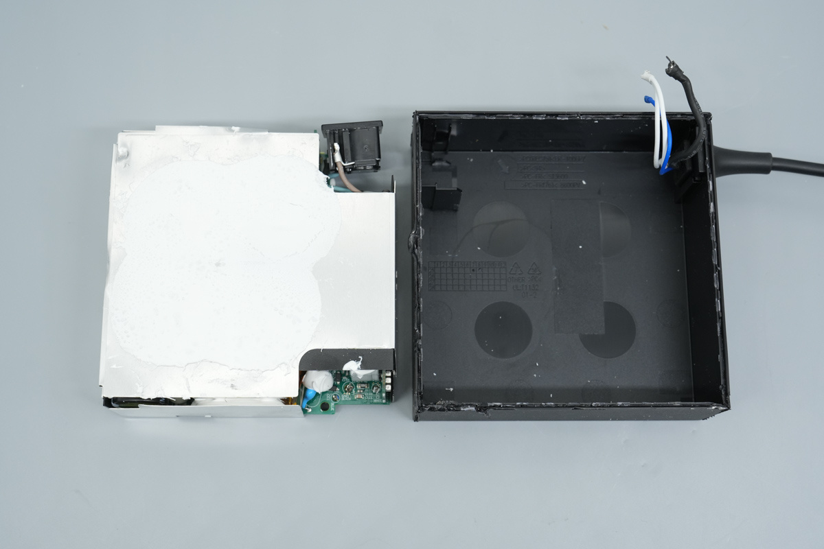
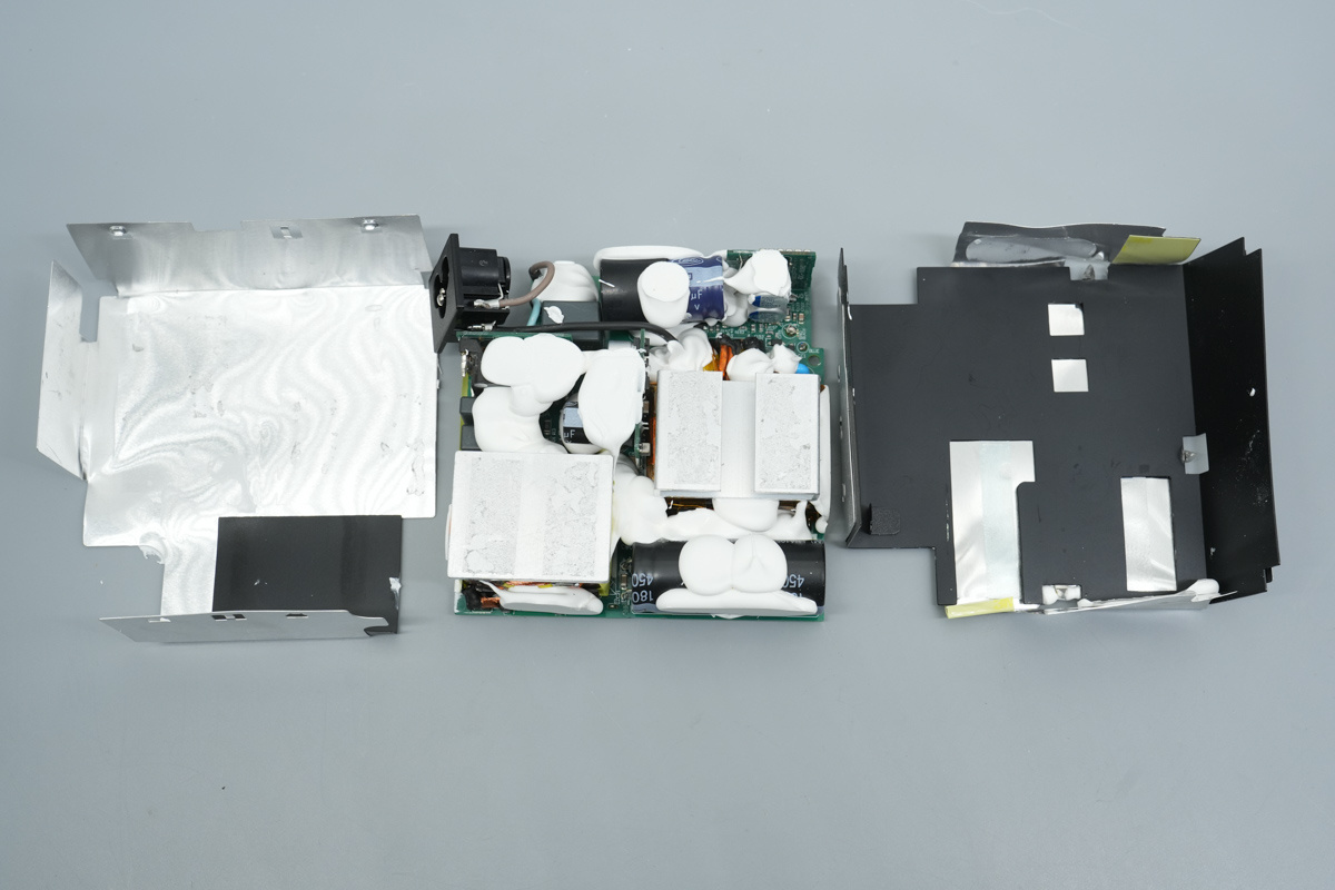
Upon fully extracting the entire thermal module and PCBA from the bottom housing, it can be seen that the interior of the bottom case is well-made and solid.
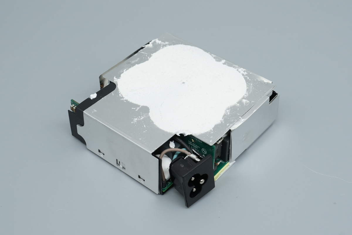
The entire PCBA is encapsulated within an aluminum alloy heatsink, with a large amount of white thermal potting compound applied to the top.
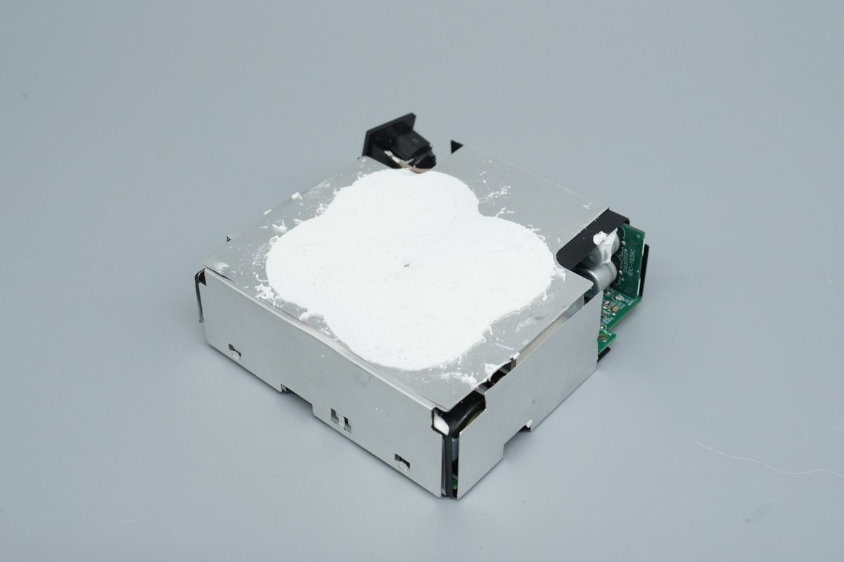
Looking at it from another angle, we can see that the AC input socket is connected to the PCBA via wires.
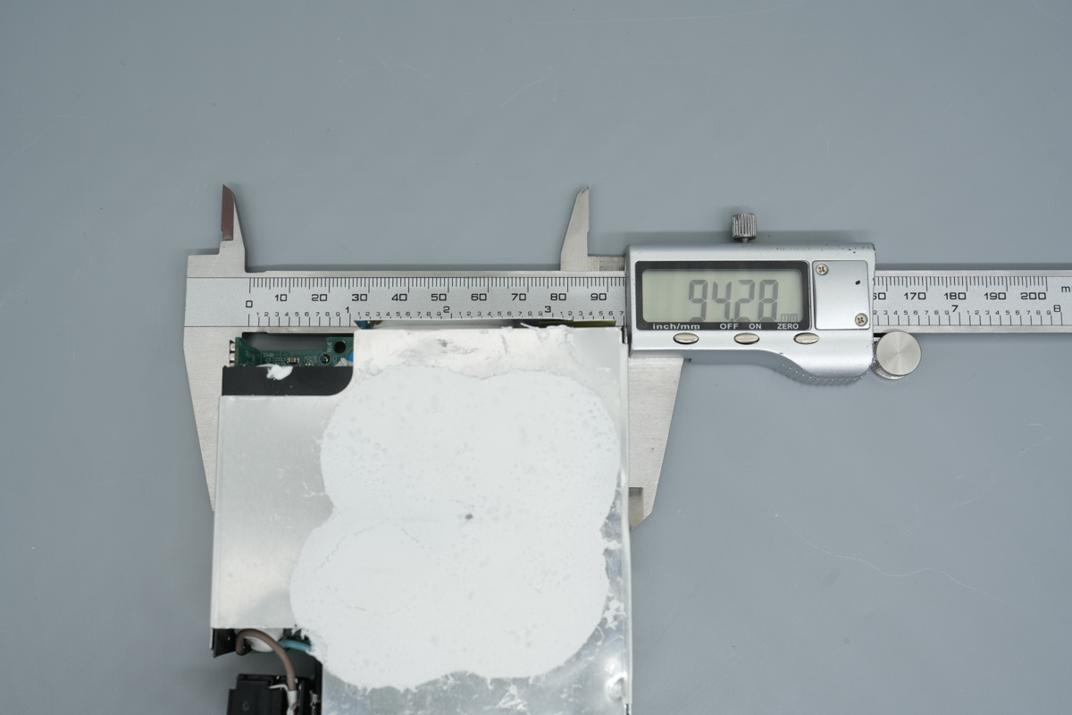
The length of the PCBA is about 94.28mm (3.897 inches).
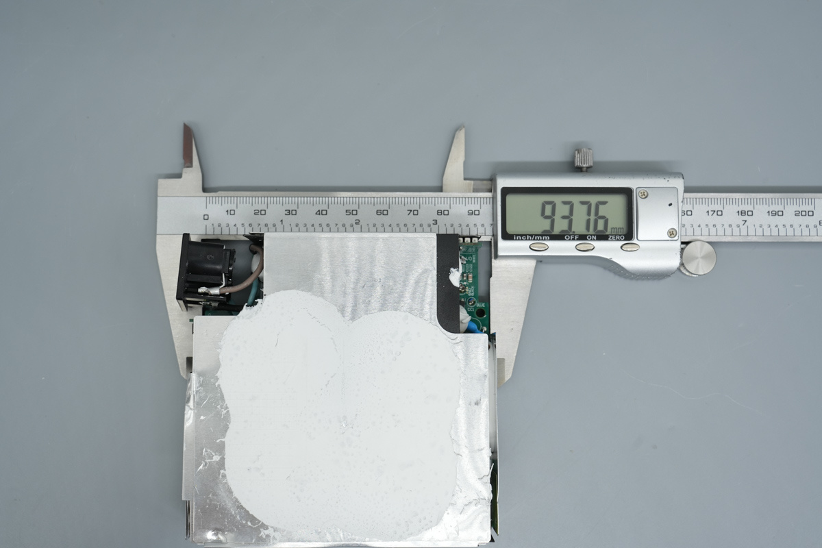
The width of the PCBA is about 93.76mm (3.691 inches).
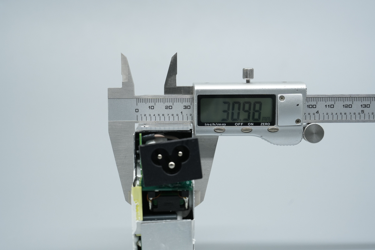
The thickness of the PCBA is about 30.98mm (1.220 inches).
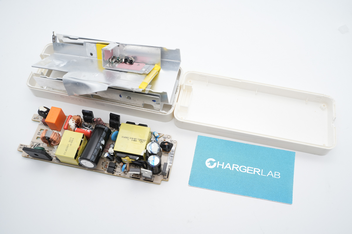
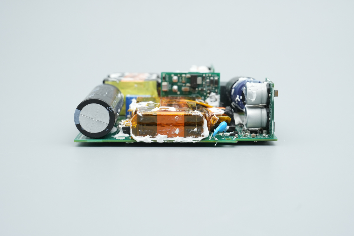
Upon removing the upper and lower metal shells, we observe that the PCBA is fully filled with white thermal potting compound. Inside the metal shells, there are plastic insulating sheets and graphite heat dissipation stickers to enhance the product's heat dissipation efficiency.
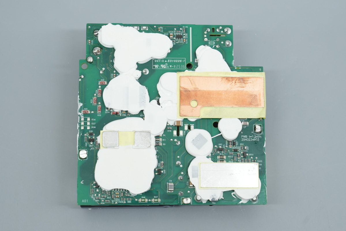
A large area of thermal compound covers the high-heat regions on the back of the PCBA, and the right side features a yellow insulating Mylar sheet layered with copper foil for local heat dissipation and shielding.
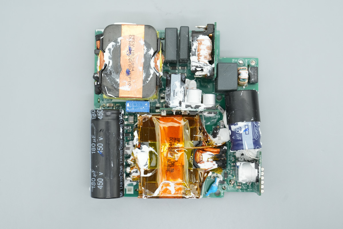
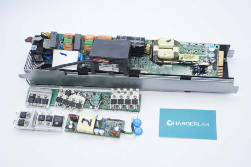
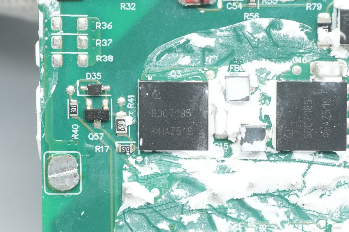
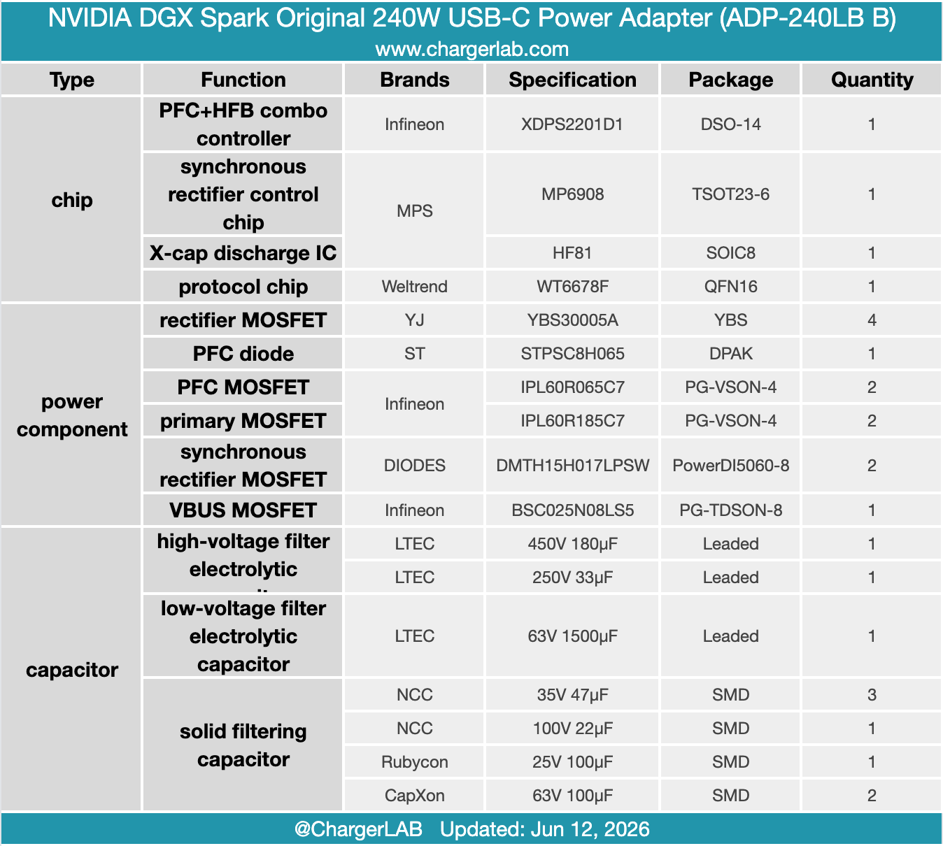
After removing the white thermal potting compound from the top, the layout of the PCBA components is clearly visible. It mainly includes an input filtering circuit, high-voltage filter caps, a PFC boost choke, a transformer, and output filtering components on the right. The module utilizes a PFC+HFB+SR architecture.
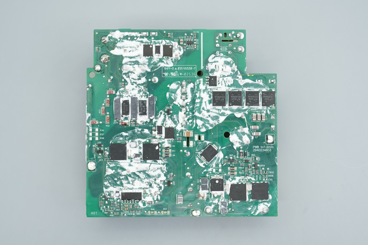
Upon cleaning the white thermal potting compound and removing the heatsink from the PCBA back, the rectifier bridge, the PFC+HFB controller, the synchronous rectifier chip, optocouplers, as well as the PFC rectifier, PFC MOSFETs, and primary switch MOSFETs are clearly visible.
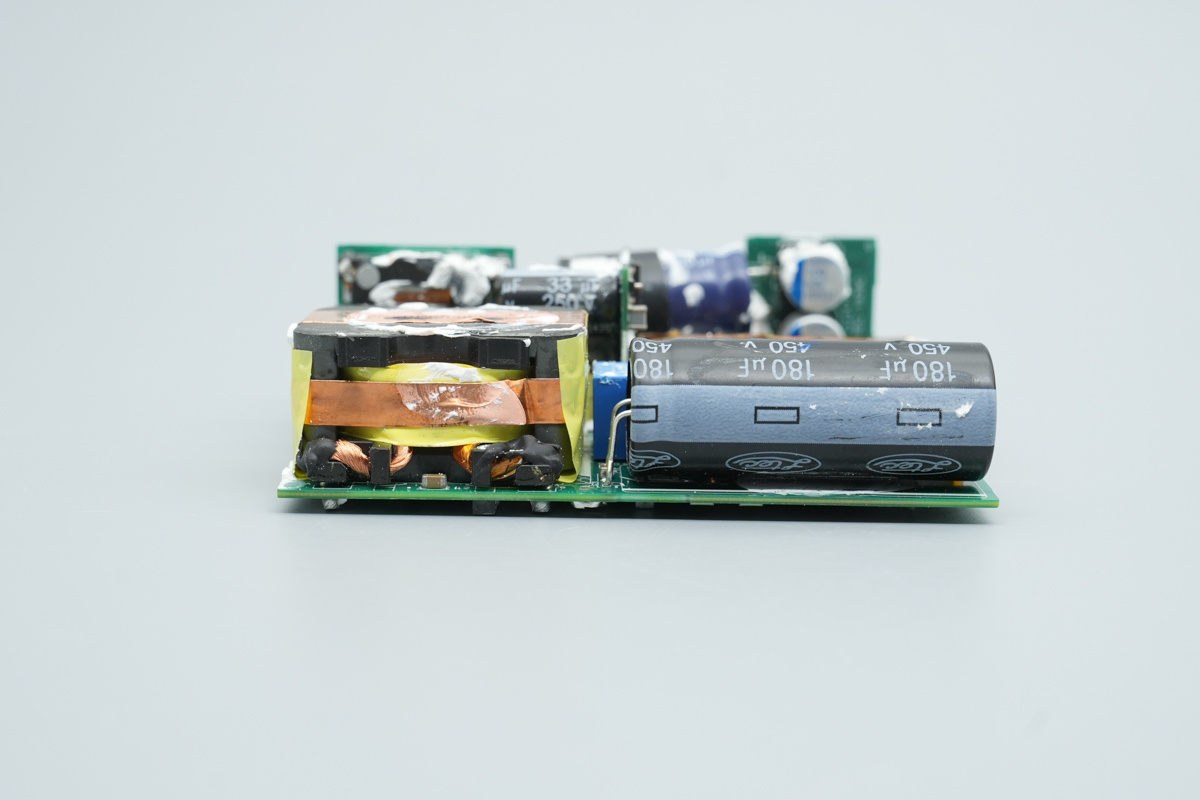
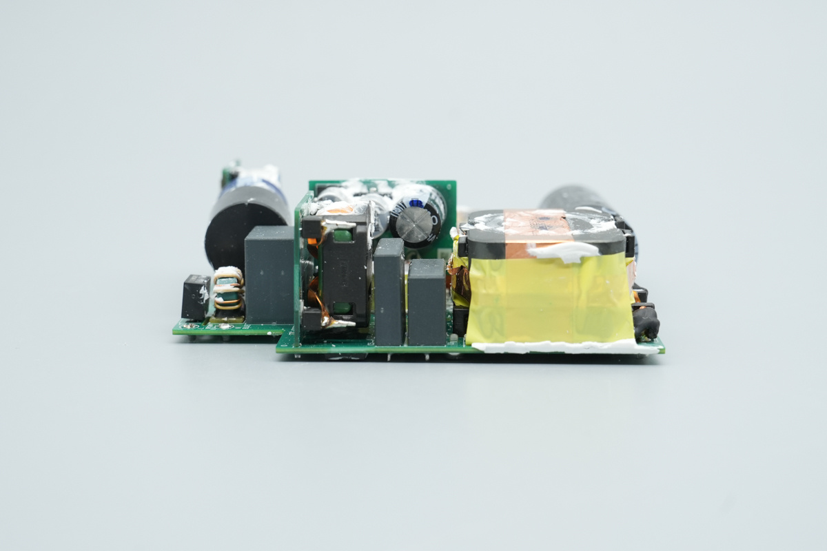
One side is equipped with a PFC choke and a high-voltage filter electrolytic cap, which is oriented horizontally to significantly reduce the overall profile of the unit.
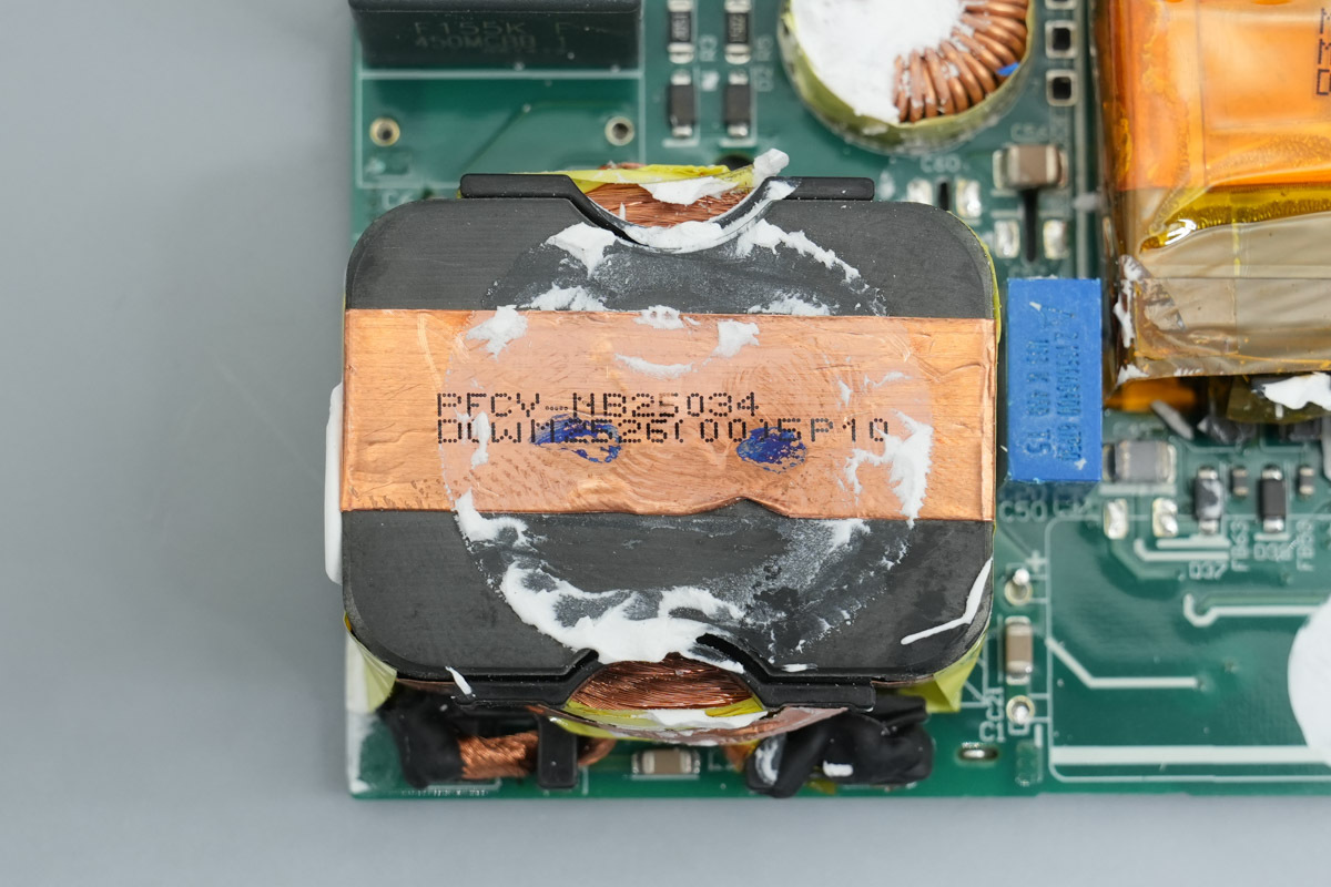
The other side houses the main transformer and some secondary filter components, with the transformer wrapped in yellow high-temperature tape for insulation.
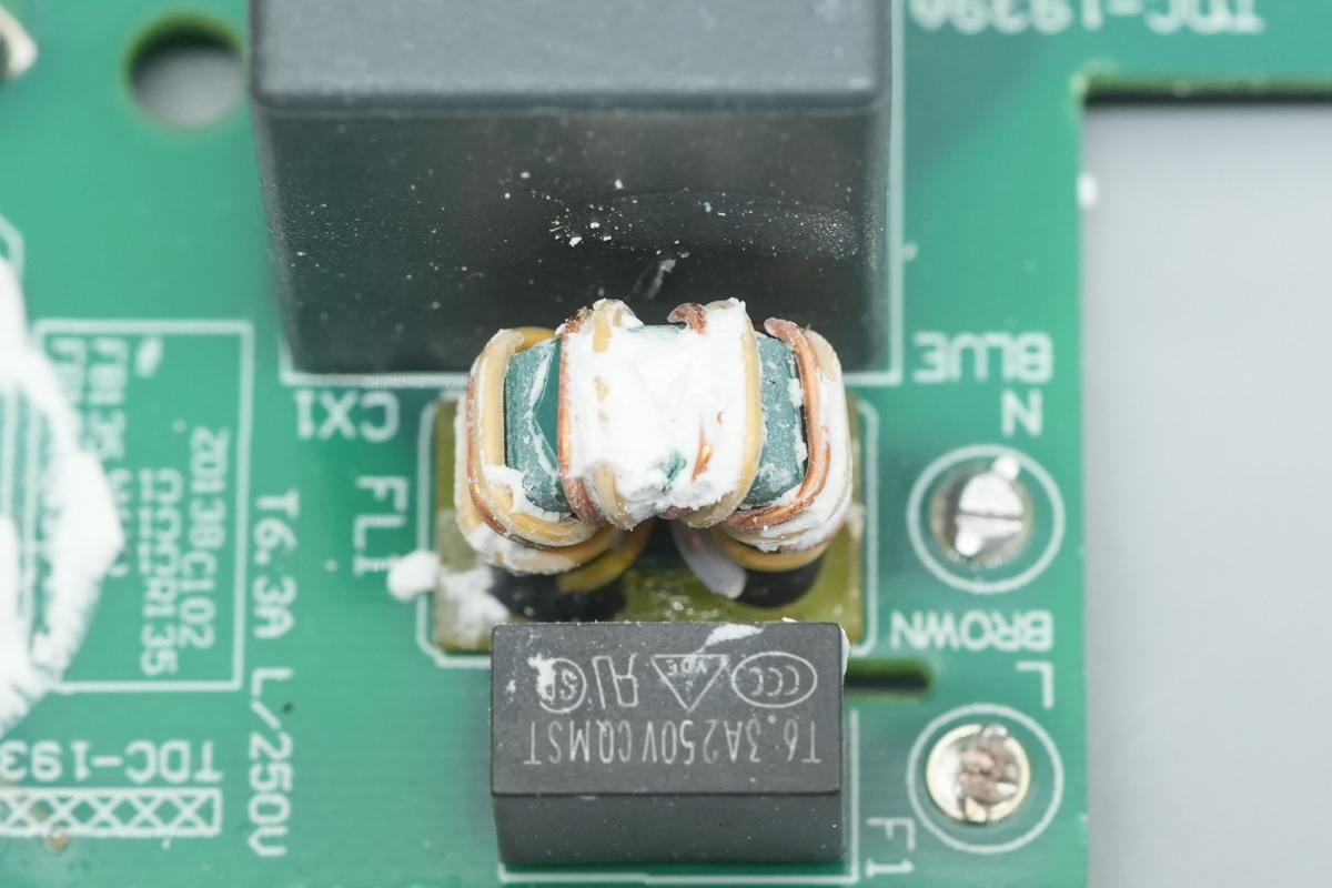
On the AC input end, we can see multiple EMI filtering circuit components, safety caps, fuses, and other safety components.
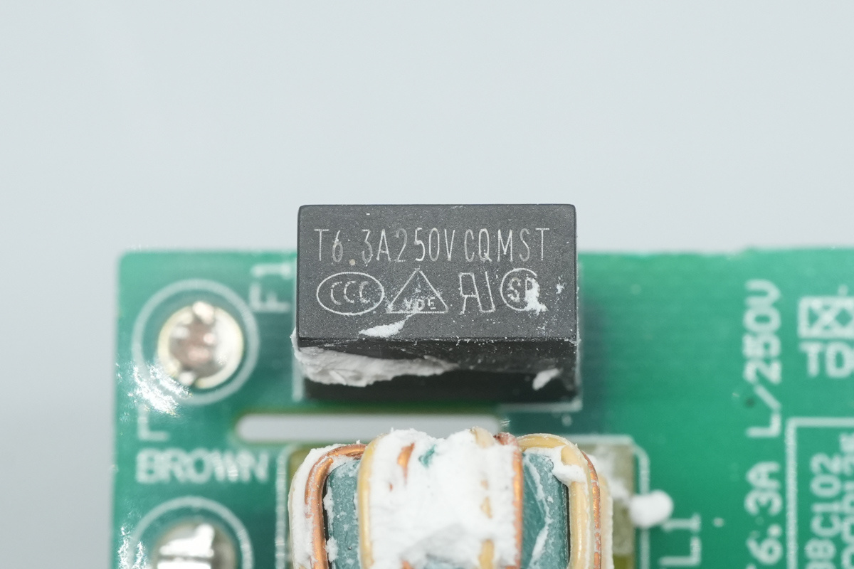
The input time-delay fuse is from Conquer, and is an MST series time-delay fuse, spec 250V 6.3A.
The common-mode choke features a bakelite insulation on the base to filter out EMI interference.
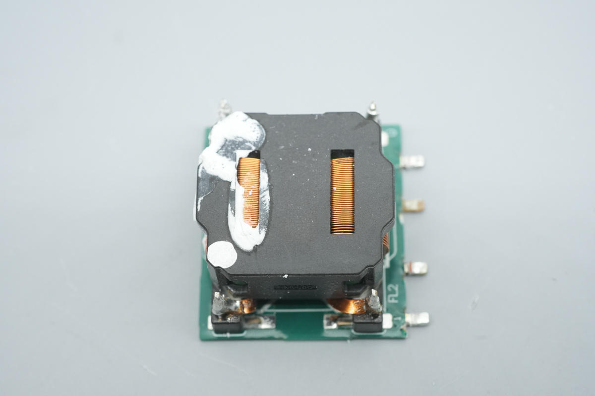
The common-mode choke is wound with flat copper wire and has a plastic casing.
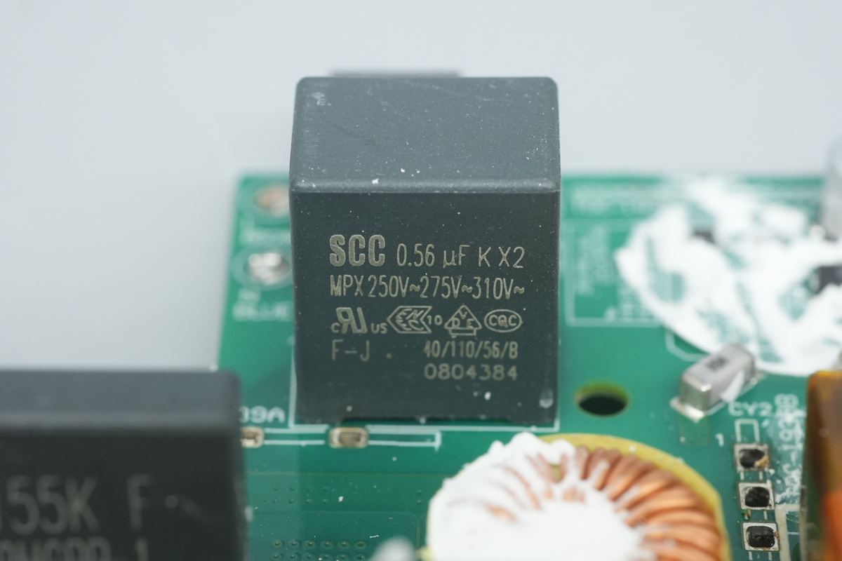
The X2 safety cap is from SCC, 0.56μF.
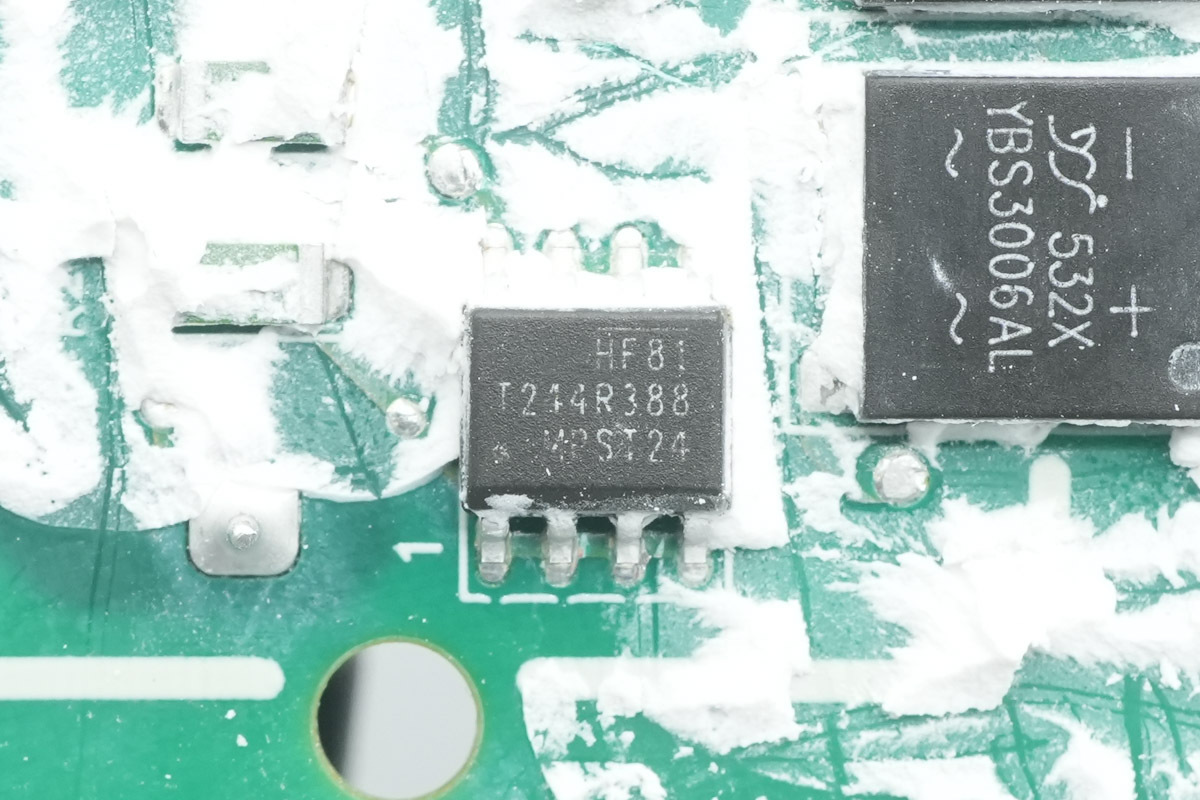
The X-cap discharge IC is from MPS, model HF81, housed in an SOIC8 package.
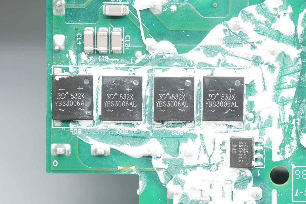
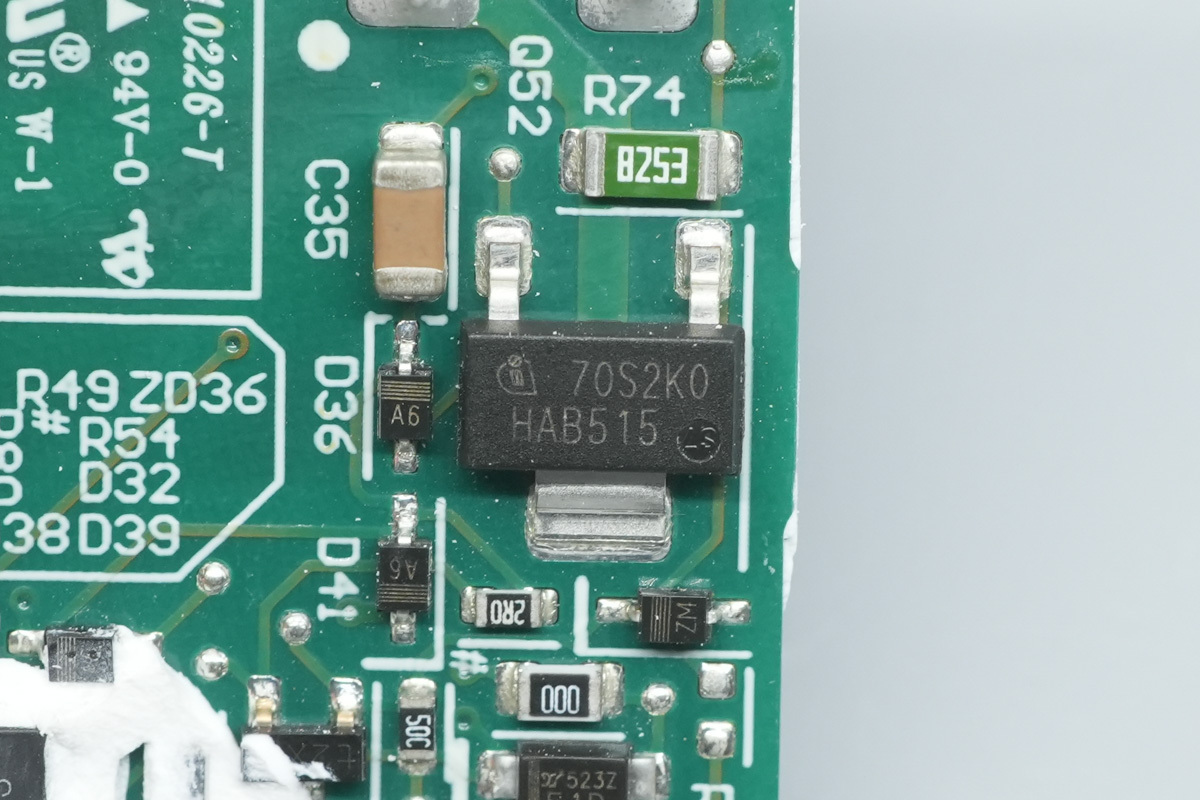
The four rectifier MOSFETs are from YJ, model YBS30005A, spec 600V 3A, and in a YBS package.
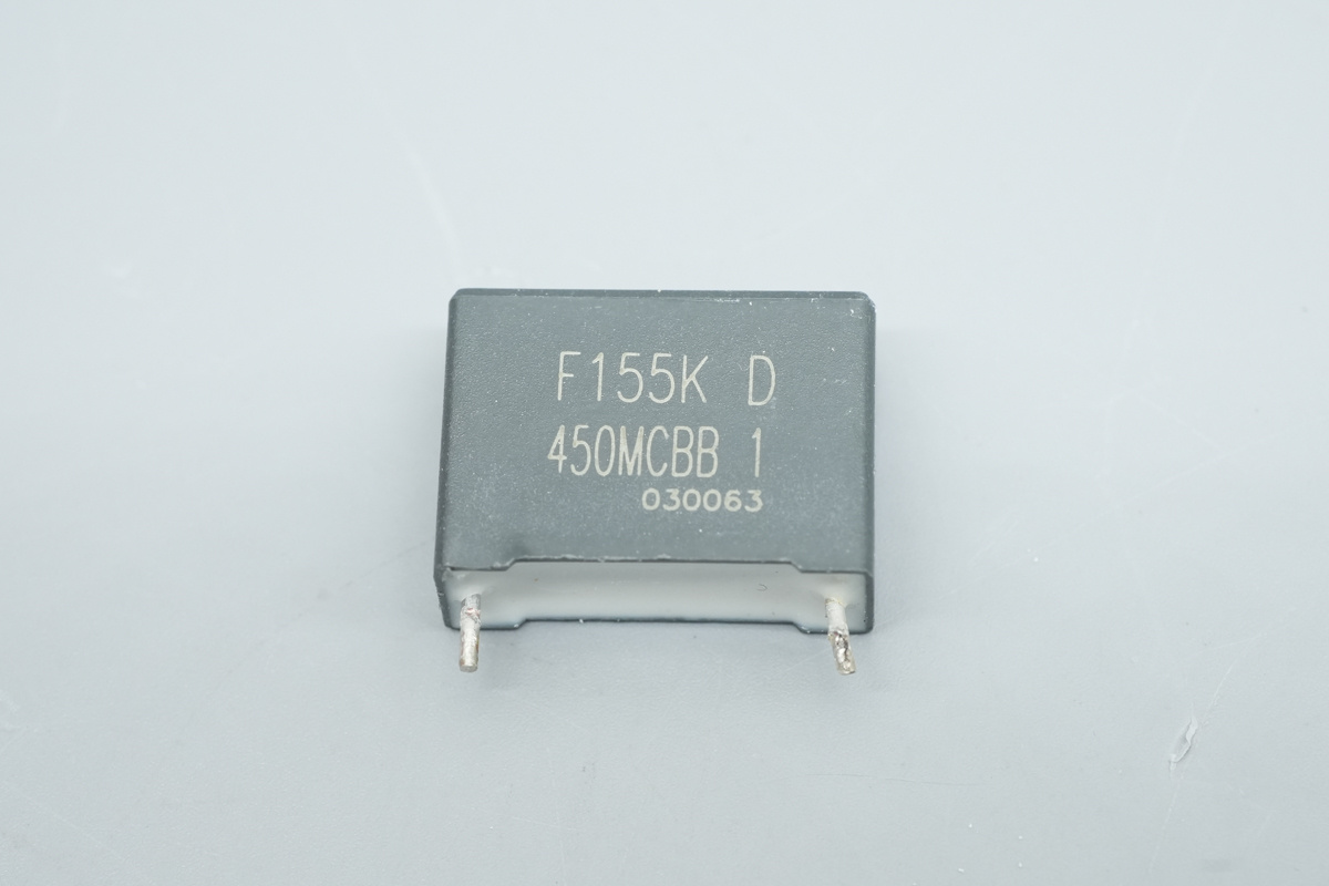
The film filtering cap, 1.5μF 450V.
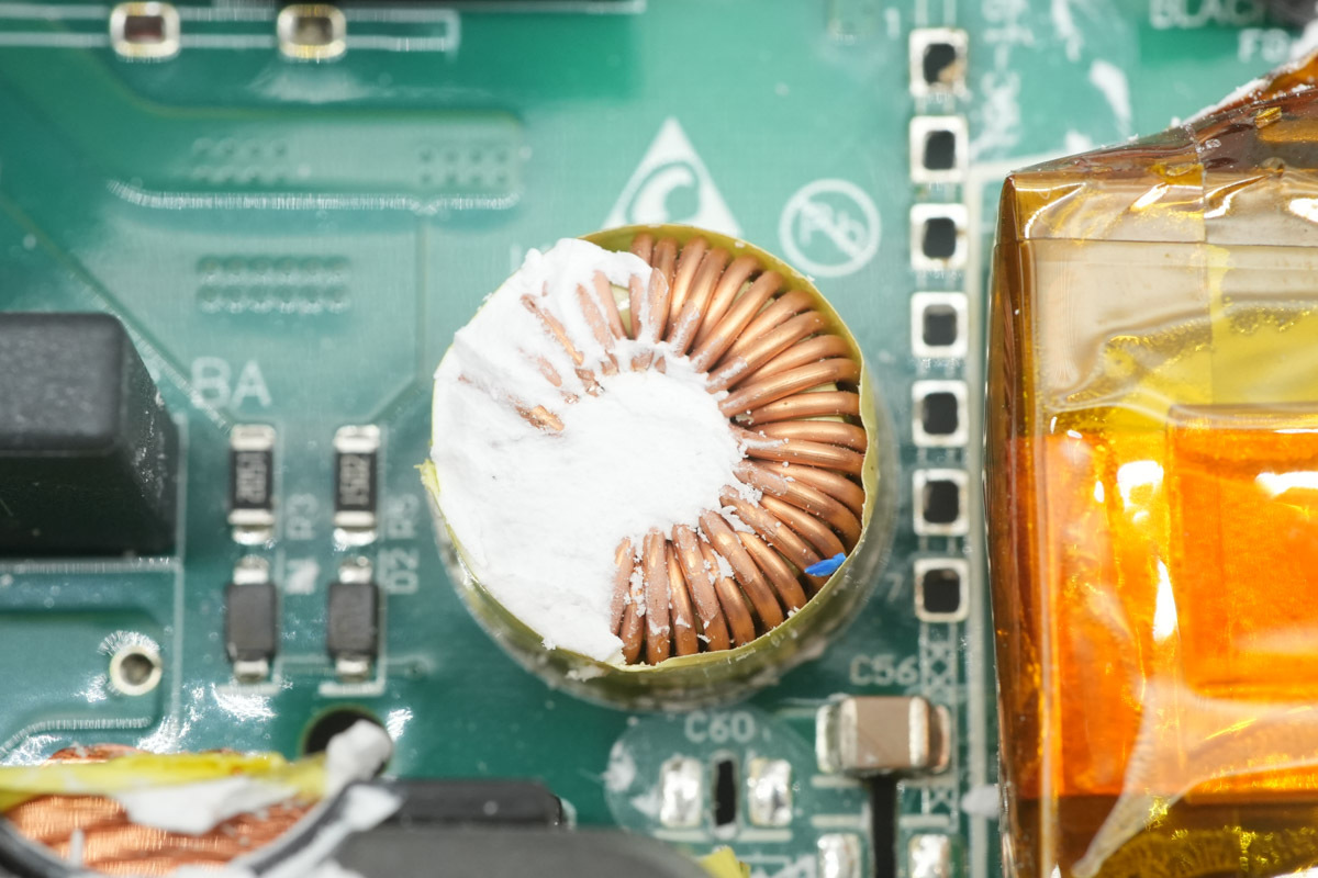
The filtering choke is secured with a large amount of white thermal potting compound.
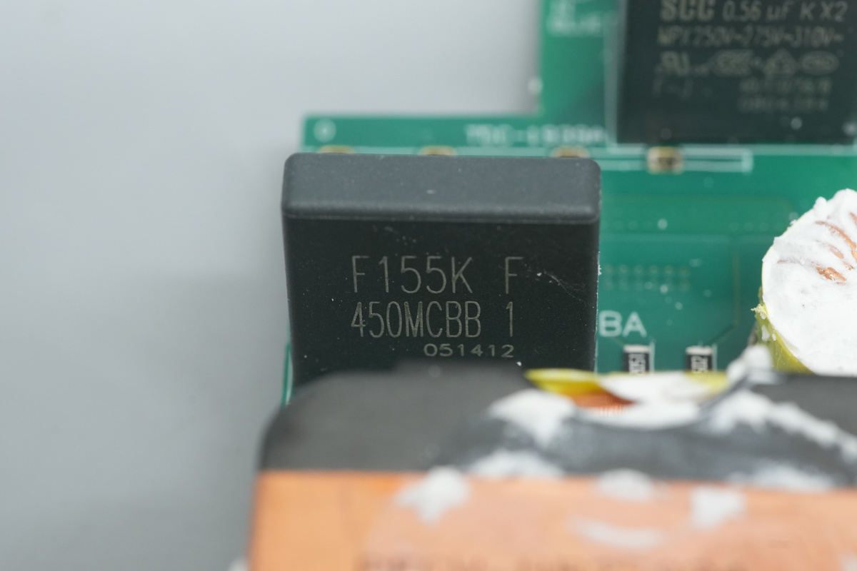
Another one shares the same model.
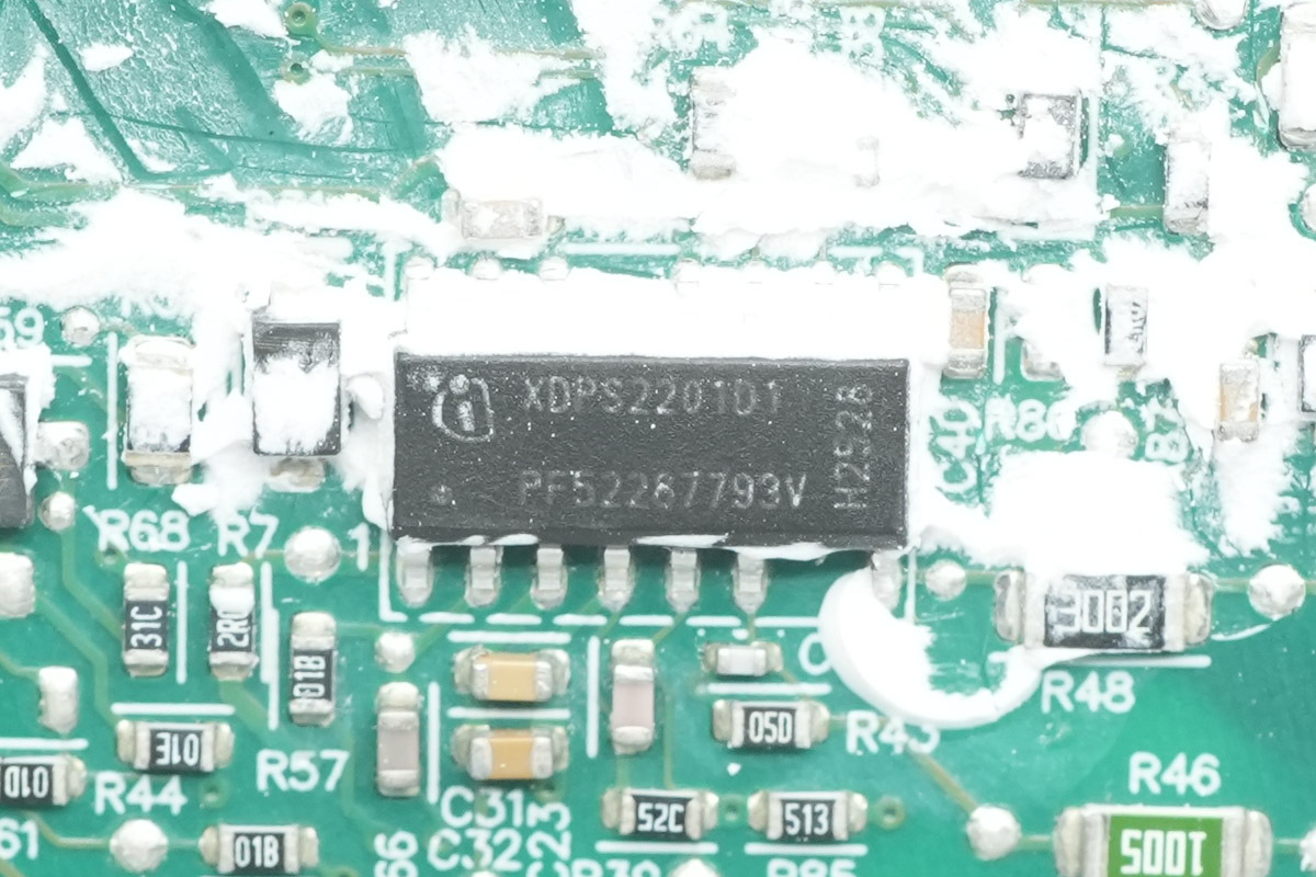
The primary control chip is from Infineon, marked XDPS2201D1, a digital hybrid-flyback controller that integrates both PFC and HFB stages. It features an internal 600V high-voltage startup circuit and high/low-side MOSFET drivers. Utilizing peak-current-mode control, it ensures rapid load response.
The IC automatically transitions to burst mode based on output current levels to optimize efficiency and supports primary-side overvoltage protection. With a standby power consumption of <75mW and a single-pin UART interface for parameter configuration, it comes in a DSO-14 package, facilitating a simplified peripheral design.
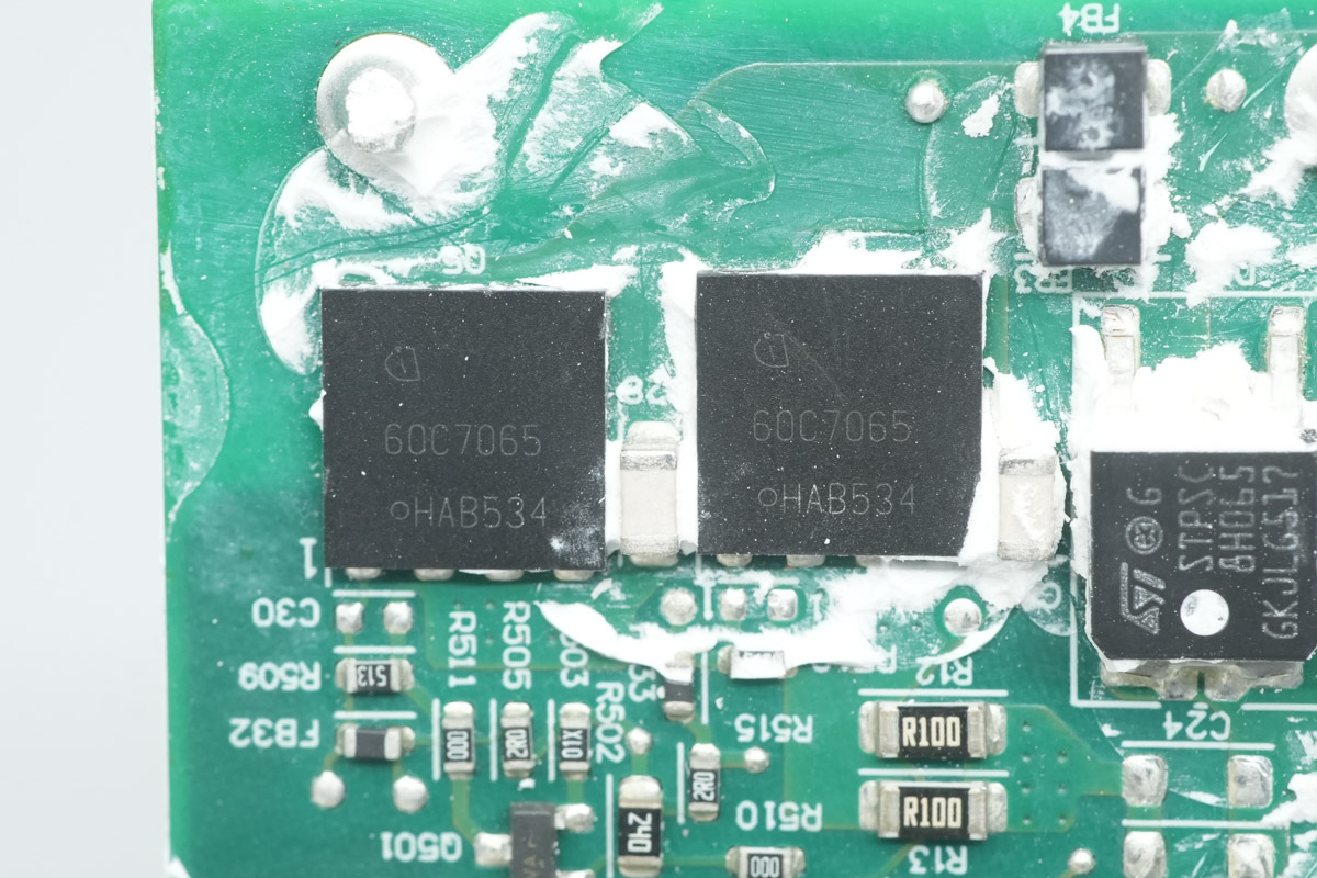
Two PFC MOSFETs are from Infineon, model IPL60R065C7, NMOS, 650V and 65mΩ, housed in a PG-VSON-4 package.
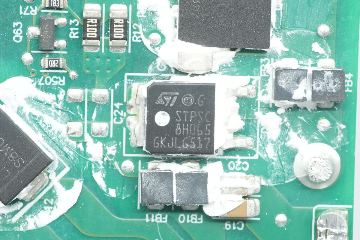
The PFC diode is from ST, model STPSC8H065, and is a 650V 8A SiC diode in a DPAK package.
Here is the PFC boost choke.
The high-voltage filter caps is from LTEC.
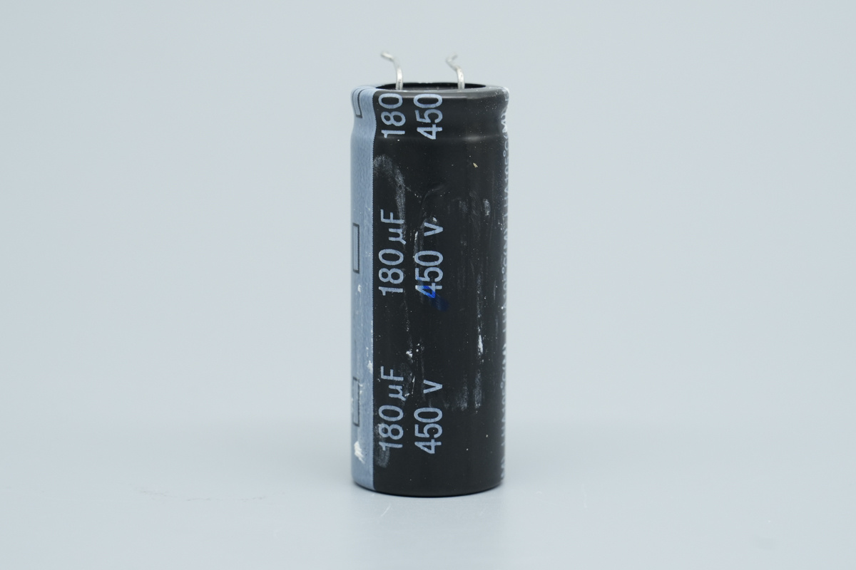
Spec 180μF450V.
Two primary MOSFETs are from Infineon, model IPL60R185C7, 650V and 185mΩ, NMOS, and in a PG-VSON-4 package.
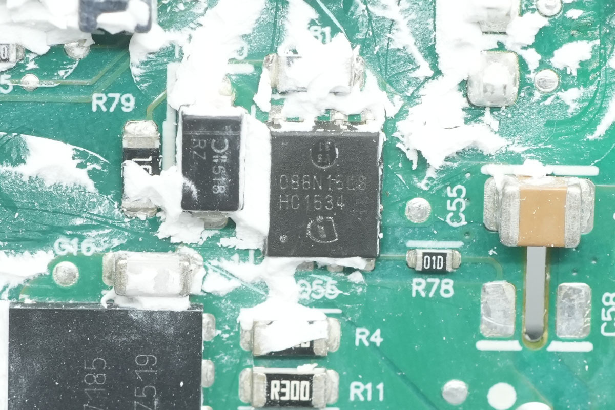
The other one is also from Infineon, model BSC088N15LS5, 150V and 8.8mΩ, NMOS, and in a PG-TDSON-8 package.
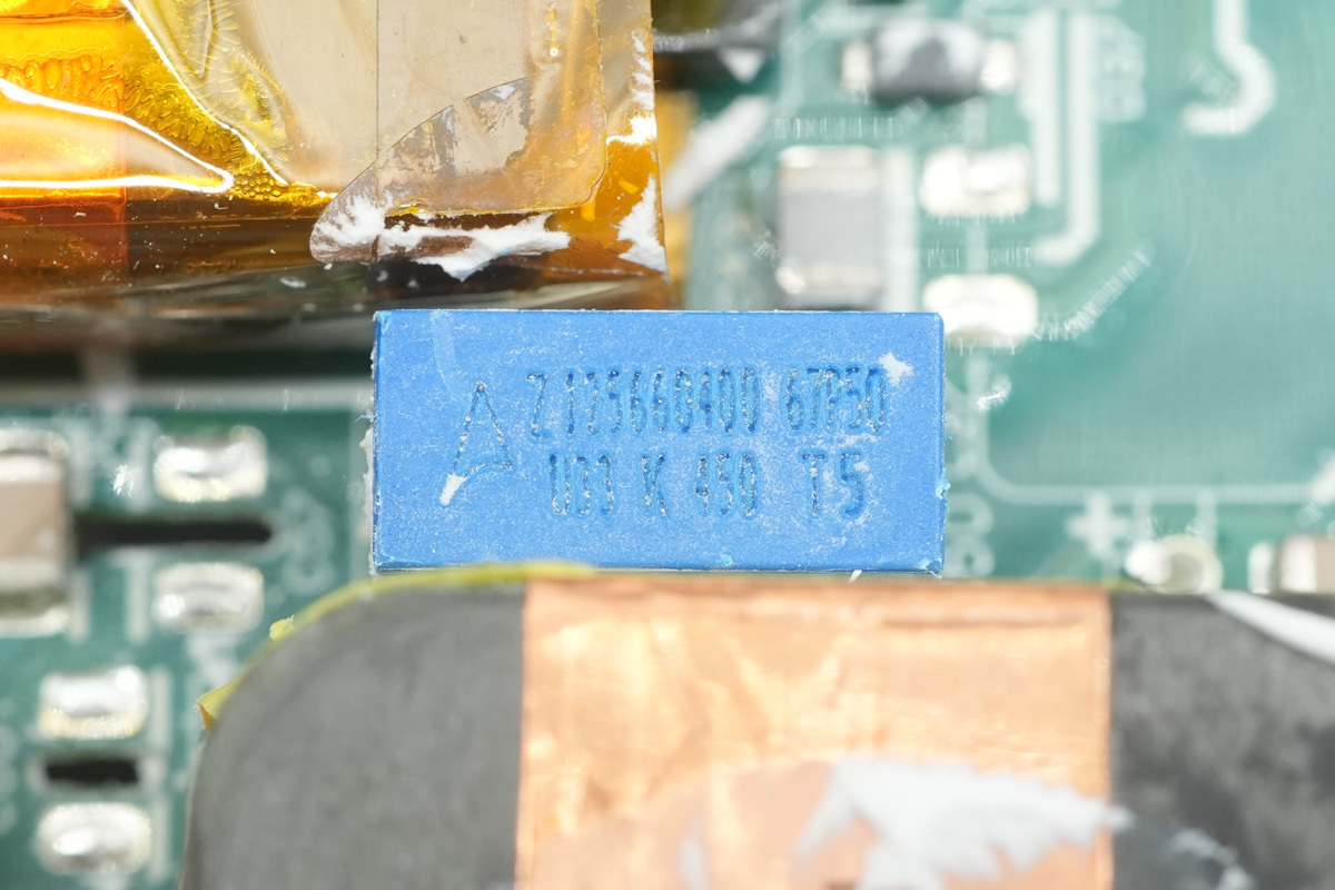
The blue film cap is from TDK.
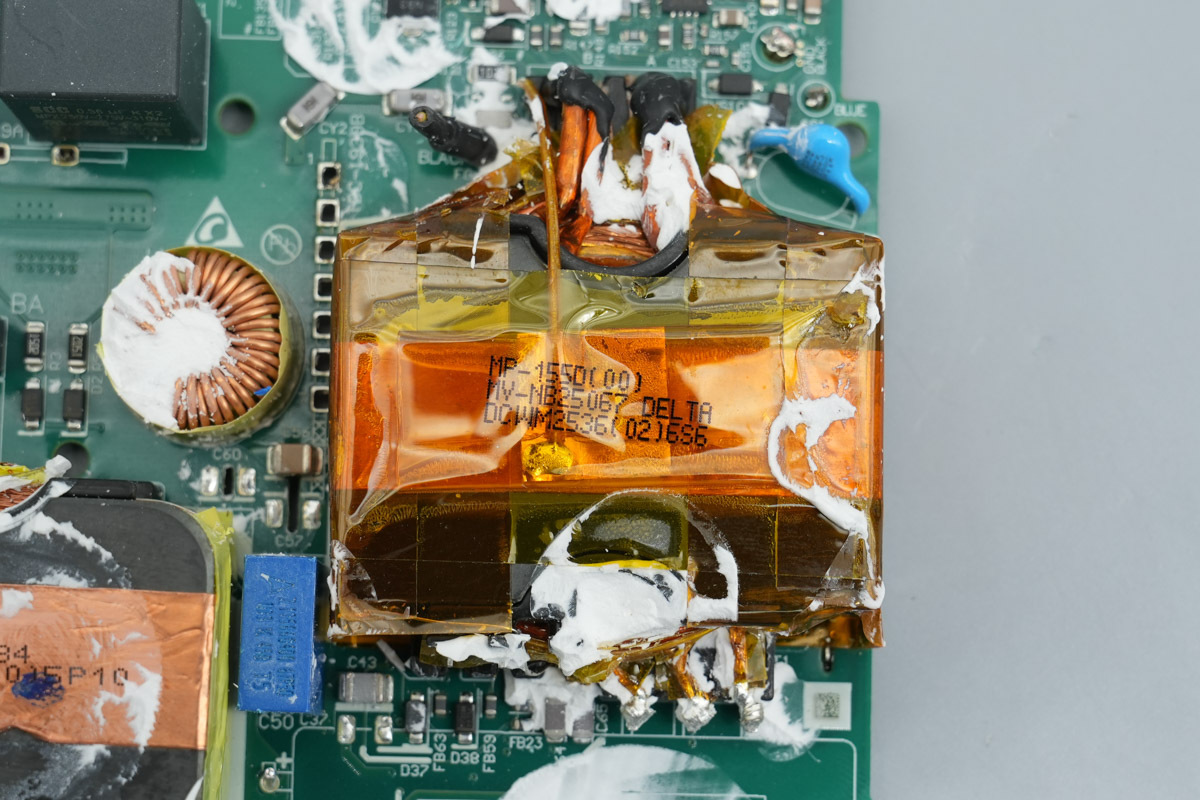
The transformer, wrapped in yellow insulating tape, which is from Delta, and the magnetic core is shielded with copper foil.
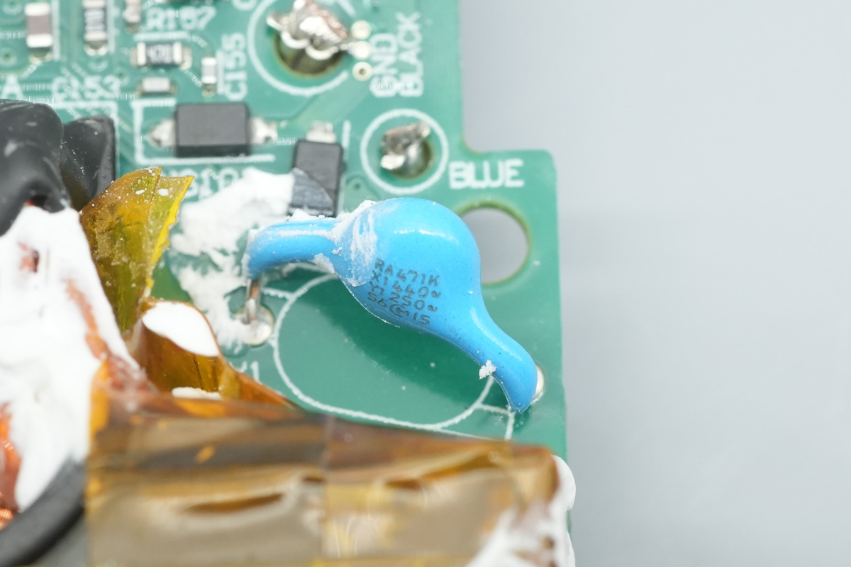
The blue safety Y-cap is from muRata, model 471K.
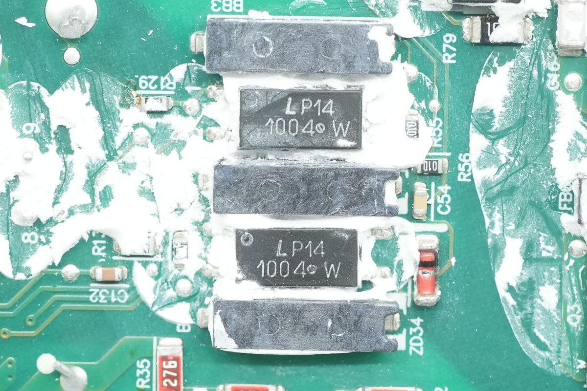
The optocoupler is from LITEON, model LTV-1004, used for feedback and protection control
The synchronous rectifier control chip is from MPS, model MP6908L, housed in a compact TSOT23-6 package. This intelligent, fast-turn-off controller eliminates the need for auxiliary windings.
By precisely driving external MOSFETs to replace conventional Schottky diodes, it significantly boosts the conversion efficiency of the flyback power supply. The IC features an internal high-voltage regulator for self-supply, supports a wide output range down to 0V, and includes ringing detection to prevent false conduction.
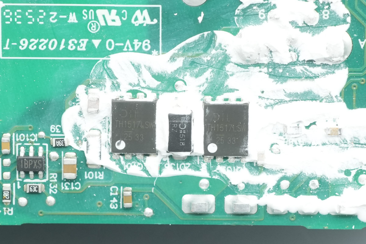
Two synchronous rectifier MOSFETs are from DIODES, model DMTH15H017LPSW, 150V and 17.5mΩ, and in a PowerDI5060-8 package.
A PCB is populated with multiple filtering caps dedicated to power for the master control chip.
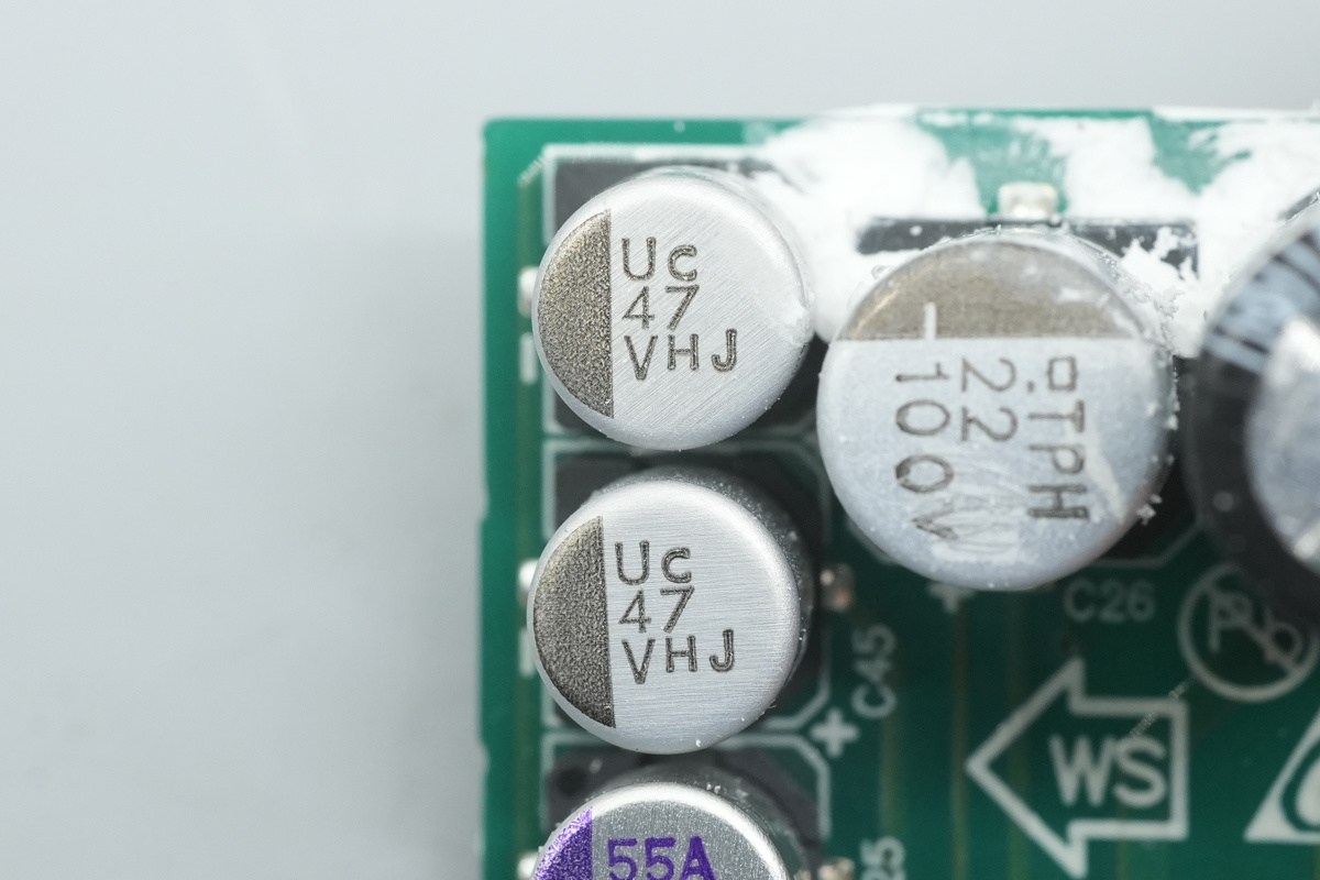
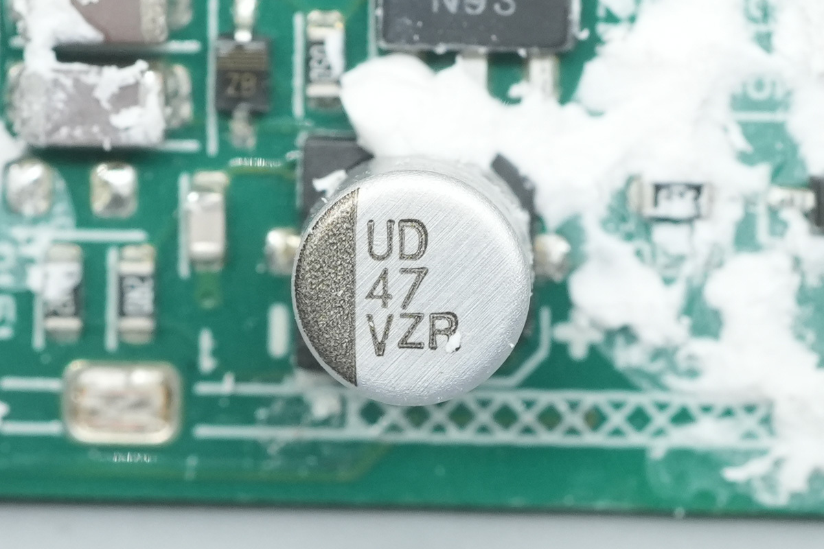
The SMD electrolytic caps are from NCC, specifically the MHJ series. These are rated for 125°C high-temperature operation, spec 47μF and 35V.
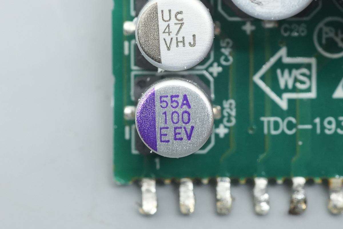
The SMD cap is from Rubycon, specifically the PEV series. These are the conductive polymer aluminum hybrid caps, 100μF at 25V.
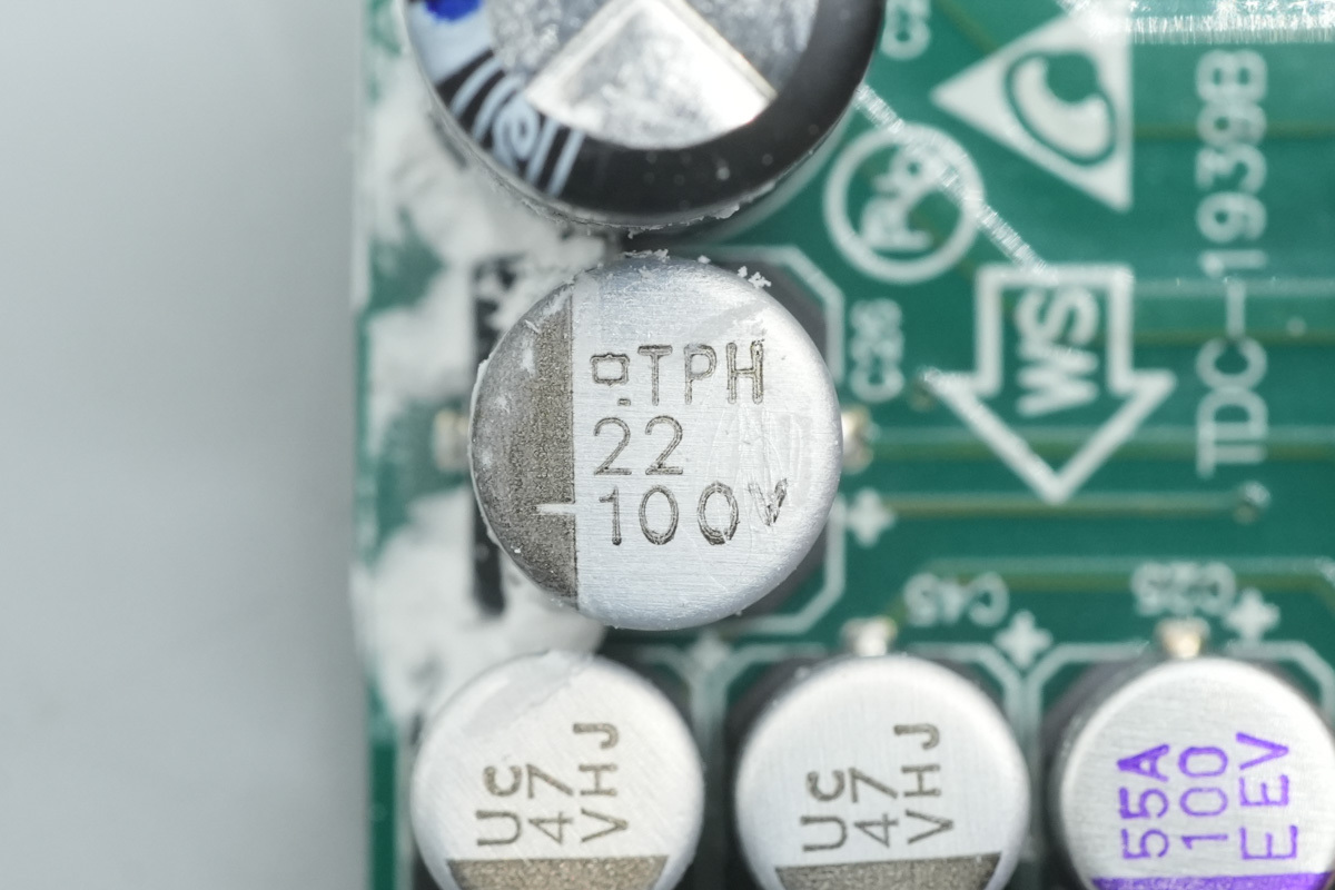
Another one is also from NCC, belonging to the MVH series. This 125°C-rated component is specified at 22μF, 100V.
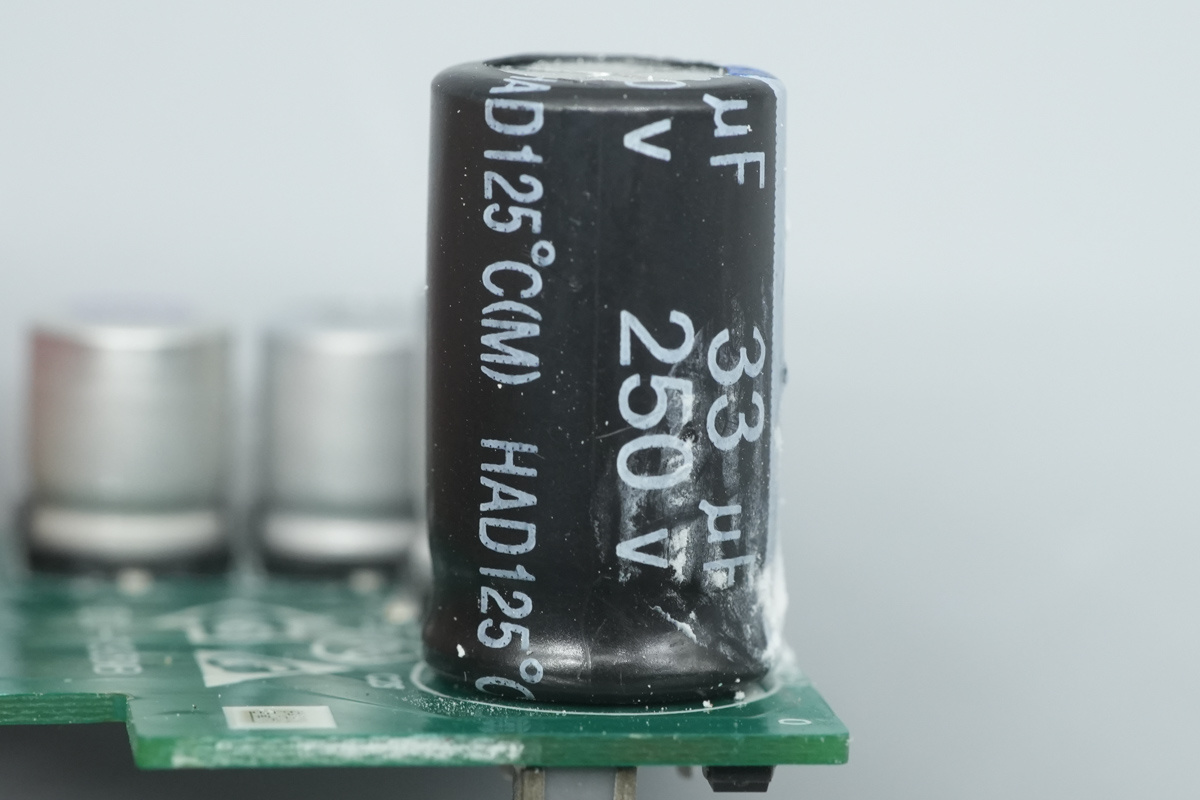
The high-voltage filter cap is from LTEC, 33μF and 250V.
The back of the PCB features a N-channel MOSFET from Infineon, model IPN70R2K0P7S, 700V and 1.64Ω, and in a SOT-223 package.
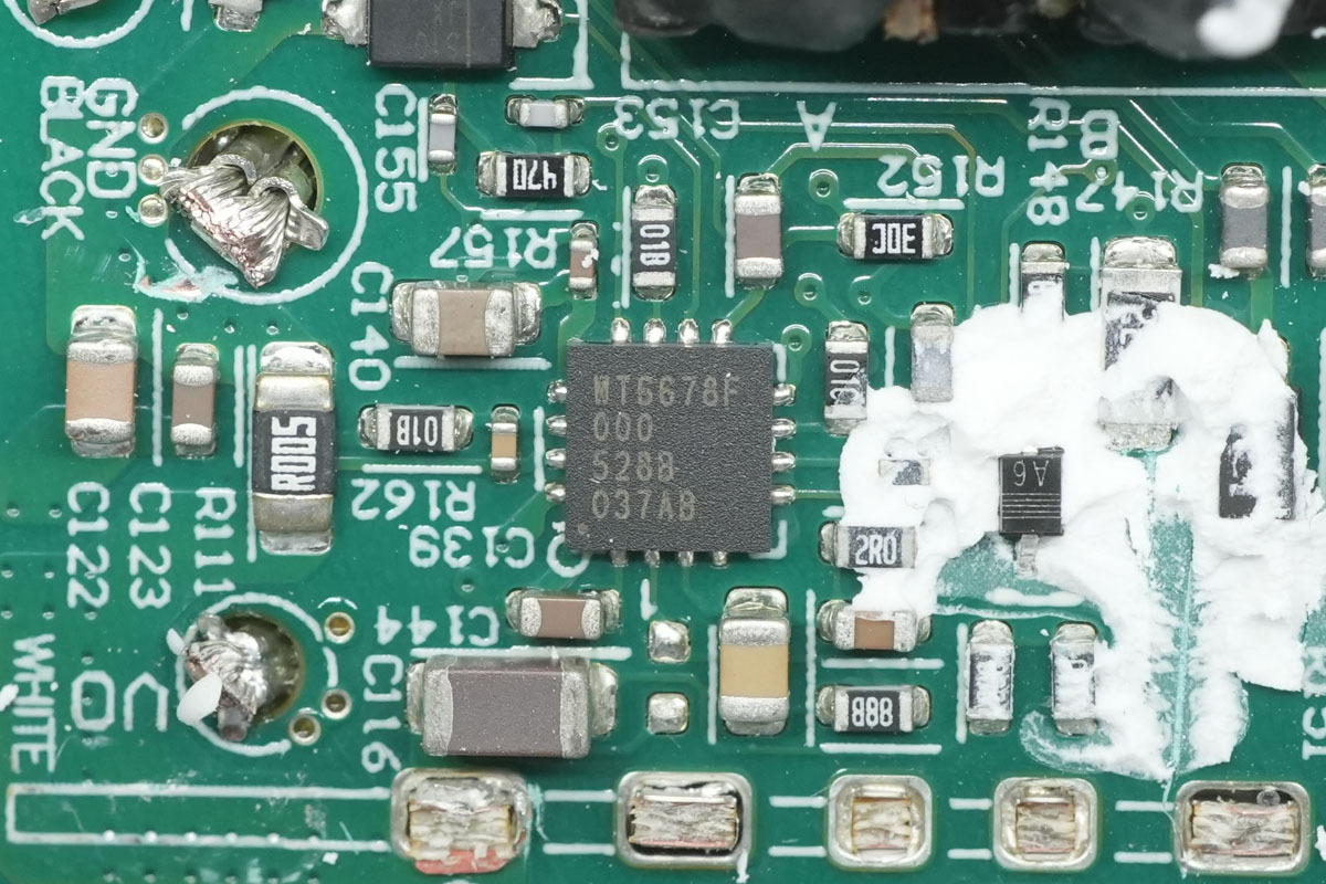
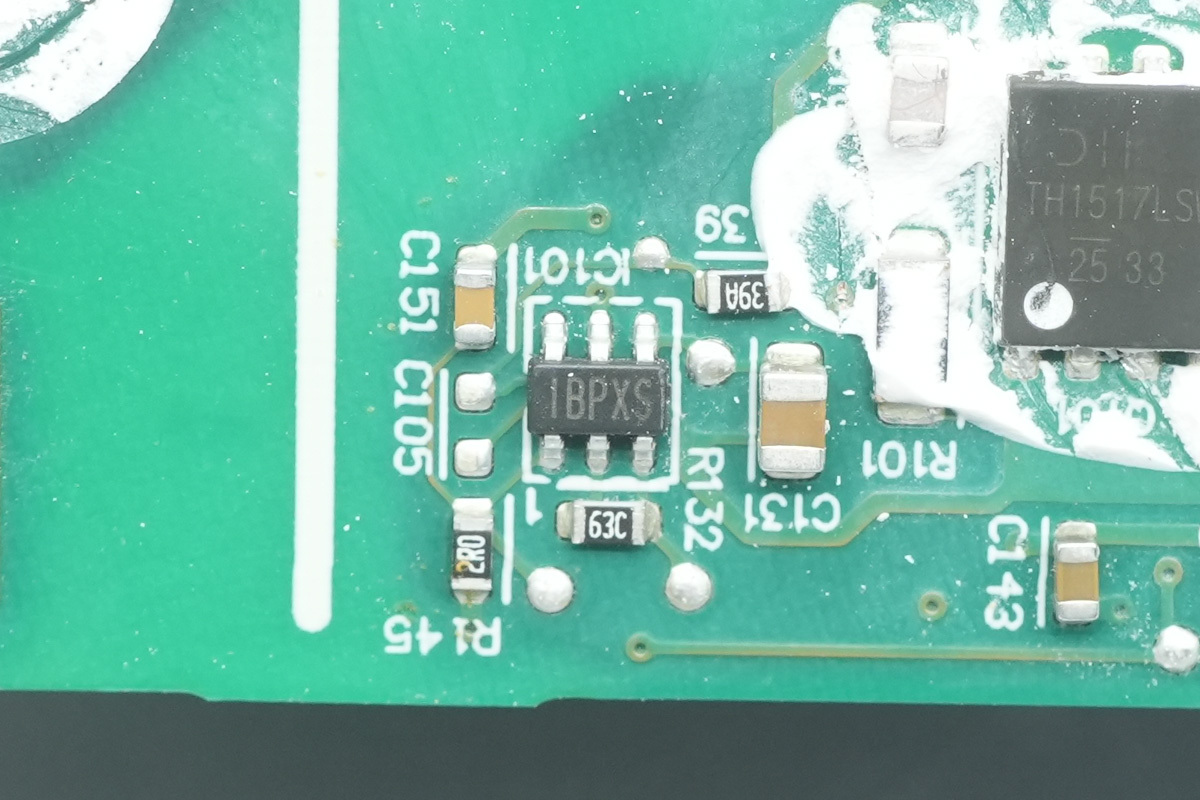
The protocol chip is from Weltrend, model WT6678F, housed in a QFN16 package. It is a highly integrated IC supporting USB PD 3.1 SPR and EPR up to 48V. It features an integrated PD PHY, USB Type-C detection logic, V/I monitors, an MCU, and gate drivers. It supports a wide operating voltage range from 3.3V to 56V.
A SMD cap is from NCC, specifically the MZR series. It is rated for 105°C operation with a spec of 47μF and 35V.
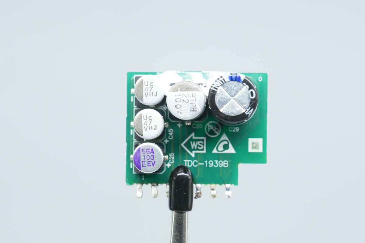
The secondary step-down output filter PCB features an array of filtering caps mounted on its top.
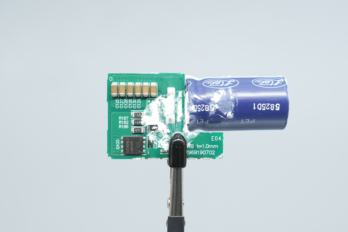
The back of the PCB features a VBUS MOSFET.
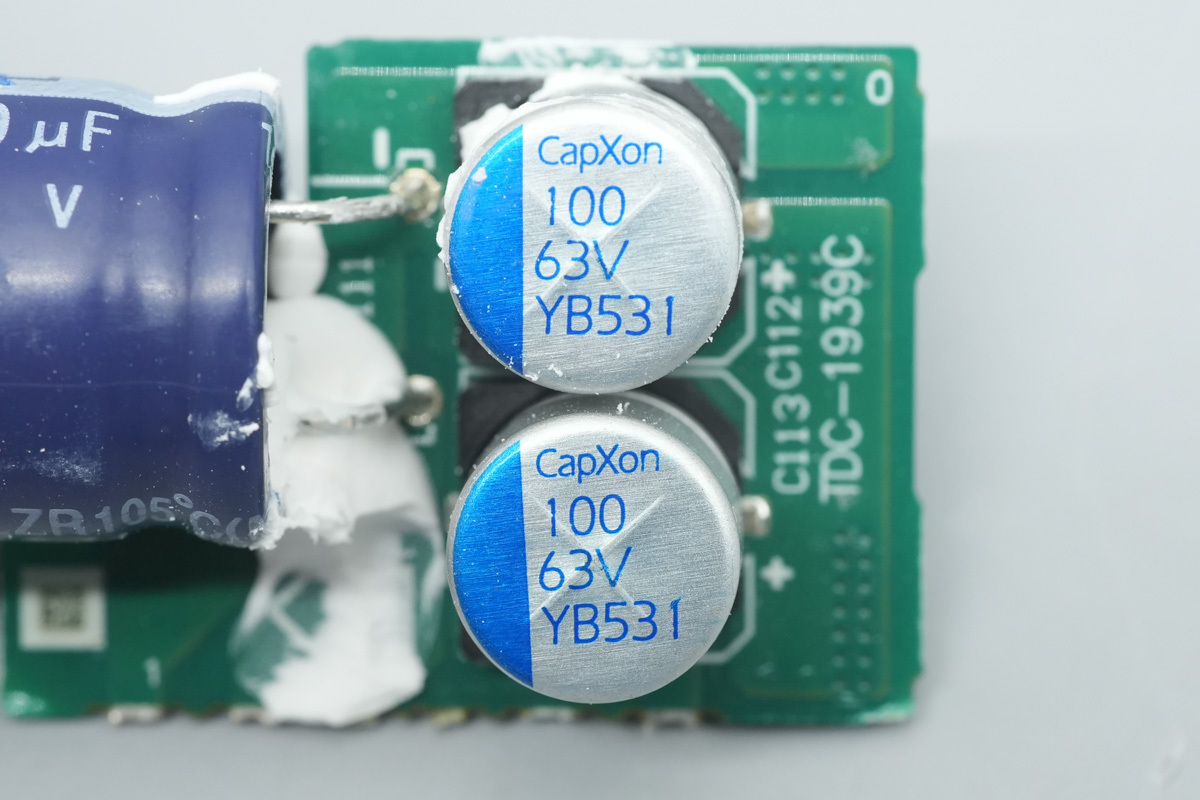
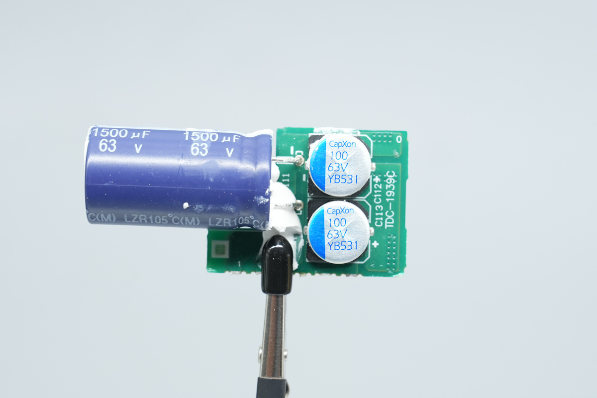
The SMD filter caps are from CapXon, which are YB series hybrid polymer caps with a heat resistance of 125℃, spec 63V 100μF.
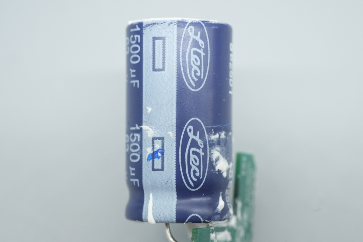
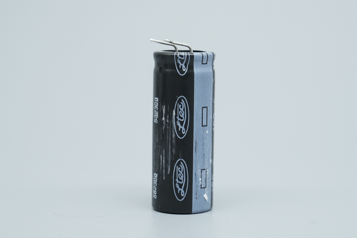
A aluminum electrolytic cap is from LTEC, 63V 1500μF.
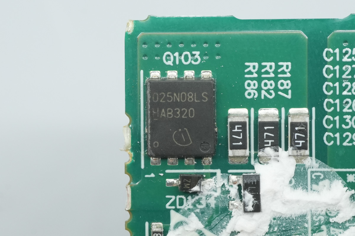
A VBUS MOSFET is from Infineon, model BSC025N08LS5, NMOS, 60V and 2.5mΩ, and a PG-TDSON-8 package.
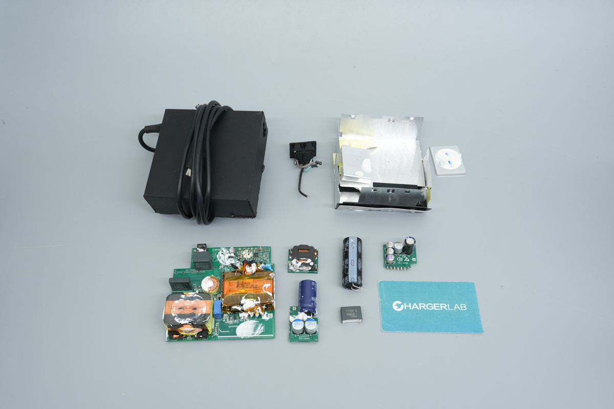
Well, those are all components of the NVIDIA DGX Spark Original 240W USB-C Power Adapter.
Summary of ChargerLAB
NVIDIA’s original DGX Spark 240W power adapter adopts a minimalist, matte-black aesthetic that feels as premium as it looks. Embossed with the signature NVIDIA logo, the design is sleek, sturdy, and practical.
Performance is a standout, with full support for PD 3.2 240W and 15V-48V AVS dynamic voltage adjustment. It is engineered to handle the demanding power and transient requirements of heavy-duty AI inference on the DGX Spark.
Under the hood, this Delta-manufactured unit is built to last. It features a fully shielded metal housing filled with thermal silicone, providing superior cooling and rugged protection against drops.
The high-performance component list is impressive: Infineon manages the PFC and primary switching, ST provides the SiC diodes for efficiency, and MPS handles rectification. Protocol duties fall to the Weltrend WT6678F, while the capacitor array features a curated mix of industry heavyweights like LTEC, Rubycon, CapXon and NCC.
Simply put, this is a top-tier power adapter—from its full-power PD 3.2 capabilities to its heavy-duty internal architecture, it’s a perfect match for the DGX Spark’s power-hungry needs.
Related Articles:
1. Teardown of the ZIENER 450W GaN TFX PC PSU
2.Tesla’s V2L goes global, New 3.5kW adapter hits the Australian and New Zealand markets
3. Teardown of AIMZENIX Mobile Gaming Keyboard and Mouse Adapter