Introduction
Up for teardown today is a 450W TFX PC PSU, sporting a sleek black aesthetic and fixed black output cables.
Designed with universal voltage support, the unit features a robust architecture: Active PFC + half-bridge LLC + synchronous rectification + DC-DC. It also leverages ZIENER’s GaN MOSFETs for enhanced performance. Join us as we strip it down to explore the engineering and high-quality components inside.
Product Appearance
The unit features an all-black exterior and comes equipped with integrated black output cables.
Output cables are secured with cable ties.
This is the 24-pin output connector for the unit.
These are the auxiliary power connectors for the unit.
The top of the chassis carries a "TFX-450W" label.
The cooling fan is equipped with a protective grille.
The side of the chassis includes grooves for auxiliary stability.
The rear of the chassis is equipped with screw holes.
The unit includes an input socket, and a label confirms support for full-range input voltage.
The output cable harness is secured using cable ties.
The width of the PSU is about 85.5mm (3.366 inches).
The height of the PSU is about 65.5mm (2.579 inches).
The length of the PSU is about 151mm (5.945 inches).
That's how big it is in the hand.
The weight is about 1035g (36.51 oz).
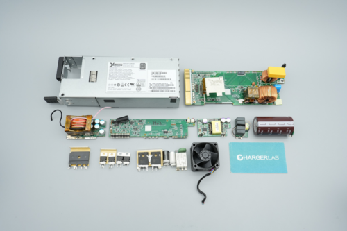
Teardown
With the aesthetic and accessory evaluation of this GaN power supply complete, we are moving on to the teardown phase.
Unscrew the fixing screws and remove the power supply casing.
The PCBA module is secured to the chassis via screws, with a Mylar sheet inserted between the PCB and the housing to provide electrical insulation.
These are the screws utilized to secure the PCBA within the chassis.
The input power cable is soldered to the PCBA.
The output cables are soldered directly to the PCBA.
The cooling fan is connected to the PCBA via a pluggable connector.
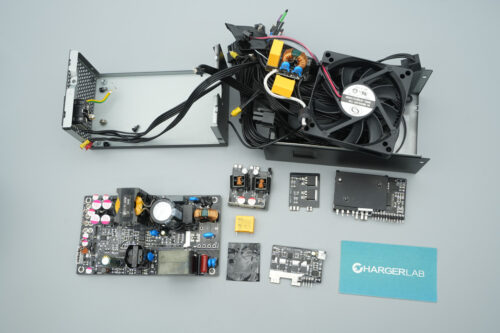
After cutting the input/output cables and removing the cooling fan, we can proceed with the disassembly.
The PCB features an X2 safety cap, a fuse, a common-mode choke, and the Y-caps.
The back of the PCB is soldered with connecting wires.
The fuse, spec 8A 250V.
The common-mode choke is wound with enameled wire.
The Y-cap pins are fitted with ferrite beads to effectively suppress high-frequency EMI.
The X2 safety cap, 1μF.
The power input cable includes a ferrite bead to effectively suppress high-frequency EMI.
The shielding plate is secured and insulated using adhesive tape.
The interior of the shielding plate utilizes soldered wire connections.
The bottom-left of PCBA hosts the AC input end, comprising common-mode chokes, X2 safety caps, and varistors. To the right, a relay and thermistor manage inrush current. Moving upward, the primary rectification and PFC stage include the rectifier bridge, Y caps, film filtering caps, and the PFC boost choke. Positioned beneath the PFC choke, the control PCB integrates the PFC control chip, PFC MOSFETs, and PFC rectifier MOSFETs.
The secondary section is equally dense, featuring high-voltage filter caps, resonant caps, an LLC MOSFET PCB, the transformer, and a synchronous rectifier PCB. A secondary step-down PCB and solid filtering caps are located on the right. Finally, the standby power supply module is centrally located at the top, housing the control chip, flyback transformer, rectifier MOSFETs, and feedback optocoupler.
There are no components on the back of the PCBA, and the copper traces for high current are exposed and tinned to enhance current carrying capacity.
After desoldering and removing the PCBs, we can now fully inspect the main PCBA and its underlying components.
The common-mode choke uses enameled wire, and a Bakelite plate is installed underneath for insulation.
The X2 safety cap, 1μF.
The varistor is from Songtian Electronics, model 10D561K, is used to absorb overvoltage surges
After removing the control PCB, the rectifier bridge is visible on the bottom left, mounted to a heatsink with screws.
There is a heatsink on the back of the PCB, connected to the PCB with a thermal pad for efficient heat dissipation.
The screws have been unscrewed, allowing for the removal of the rectifier bridge and the heatsink.
The rectifier bridge is from SEP, model GBU1508, spec 15A, 800V, and in a GBU package.
The film filtering cap, 0.47μF, 400V.
The Y-cap, model JY222M, features ferrite beads to effectively suppress high-frequency EMI.
The PFC PCB contains the PFC MOSFET, SiC diode, and a combo controller.
There are no components on the back of the PCB, and a thermal pad is attached to enhance heat dissipation.
The combo controller is from MPS, model HR1213, incorporates a multi-mode PFC and current-mode LLC controller. It supports both AC and DC inputs and features configurable bias options. The PFC stage operates in hybrid CCM/DCM and includes burst mode capabilities.
The LLC stage supports steady-state, jump, and burst modes, featuring adaptive dead-time adjustment and capacitive mode protection. Integrated functions include high-voltage startup, thermal shutdown, PFC switch protection, OVP, OCP, and LLC OCP. It is packaged in SOIC-20 and includes a UART configuration interface.
The PFC MOSFET is from ZIENER, model ZN65C1R070T. It utilizes a Cascode GaN structure with a 650V continuous and 800V transient voltage rating, and a 70mΩ on-resistance. The gate supports a 20V rating and features low gate charge characteristics, enabling compatibility with standard silicon-based gate drivers and simplifying drive circuitry.
It is JEDEC and RoHS compliant, optimized for both soft and hard-switching topologies to enhance power density, reduce system volume, and lower overall costs. It is packaged in TOLL, suitable for fast chargers, telecom power, data centers, and lighting applications.
Here is the info about the ZIENER ZN65C1R070T.
The PFC rectifier MOSFET is from GPT, model G3S06508D. This is a third-generation SiC Schottky diode rated at 650V and 8A. It is housed in a TO-263 package.
A 30mΩ current sense resistor is utilized to monitor the current flow through the PFC MOSFET.
The PFC boost choke, 260μH.
The relay is from Yongneng, model YX201H-S-112DM. It features one normally open contact, a 10A/250V contact capacity, and a 12V DC coil.
The NTC thermistor, marked 5D-11, is used to suppress surge current upon power-up.
The blue Y-cap, model JY222M.
The high-voltage filter cap is from Nichicon, specifically the LGG series of miniaturized electrolytic caps, which are heat-resistant up to 105℃.
Spec 330μF400V.
The LLC MOSFETs are from Oriental, model OSG60R180KF, 650V/180mΩ, NMOS, are mounted on a vertical sub-board. They are in TO-263 packages.
The resonant cap is from FARATRONIC, spec 0.082μF at 630V.
The synchronous rectifier control chip, gate driver, synchronous rectifier MOSFETs, and MCU are mounted on a vertical PCB.
The back of the PCB has exposed copper and tin to enhance heat dissipation.
The synchronous rectifier control chip is from MPS, model MP6924B. It is a dual-channel fast-shutdown rectifier for LLC synchronous rectification, and it is packaged in SOIC-8.
The gate driver is from DIODES, marked 3009, model ZXGD3009E6. It is a 1A output current driver that supports a 40V supply voltage and uses an SOT26 package.
Another one shares the same model.
The synchronous rectifier MOSFET is from ALLPOWER, model APG013N04G, NMOS, 40V and 1.1mΩ, and in a PDFN5*6-8L package.
The MCU is from FMD, model FT61E131B-RB, with built-in 3K * 14bit ROM, 256B RAM and 128B EEPROM, supports a working voltage range of 1.9-5.5V, and in an SOP8 package.
This is a thermistor used to detect temperature.
The D882 NPN BJT is used to control the cooling fan.
The filter caps are from TEAPO.
Spec 22μF50V.
This is the socket for connecting the cooling fan.
The solid filtering caps are from TEAPO, specifically the FG series polymer solid aluminum electrolytic caps, spec 1500μF 16V.
The filter choke uses a ferrite bead design.
The solid filtering cap, 470μF16V.
The rectifier diode, model ES3J.
The filter caps are from APAQ, spec 330μF 16V.
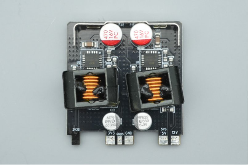
The PCB features the filtering caps, the synchronous step-down chips, and the step-down chokes, to produce stable 3.3V and 5V outputs.
The exposed copper and tin on the back of the PCB enhances current carrying capacity and improves heat conduction.
The two filter caps, 470μF 16V.
The synchronous step-down chip is from NDP, model NDP23803QB. It supports 8-18V input voltage, continuous output current of 12A, and integrates a 5mΩ MOSFET. It is packaged in a QFN5*5 package.
The step-down chokes are wound with flat copper wire.
The filtering caps are from APAQ, spec 560μF/6.3V.
A 2mΩ shunt resistor is used for monitoring the 3.3V output current.
Another one is used for monitoring the 5V output current.
The filtering caps, 560μF/6.3V.
The standby power IC is from Chipown, model PN8141. It integrates a PWM controller and 650V MOSFET in a DIP7 package. It offers ultra-low standby power, high efficiency, and built-in protections for heat, overload, overcurrent, overvoltage, and short circuits.
The filtering cap dedicated to the standby power IC, 22μF/50V.
The standby power transformer is insulated with adhesive tape to provide electrical isolation.
The optocoupler is from LITEON, model LTV-817C, is utilized for output voltage feedback.
The standby power rectifier MOSFET is from MHCHXM, model ER2EL60CS, with a withstand voltage of 60V and a TO-252-2L package.
The filter caps are from TEAPO.
Spec 2200μF16V.
This is the output filtering choke.
The output control MOSFET is from ALLPOWER, model AP180N03G, NMOS, 30V and 1.7mΩ, and in a PDFN5*6 package.
The filtering cap, 560μF6.3V.
The supervisor IC is from Grenergy, model GR8313F, a three-channel power monitoring controller. This device provides simultaneous voltage monitoring for 3.3V, 5V, and 12V output rails. It features integrated UVP, OVP, remote on/off control, and a fault signal output pin. It is in an SOP-8 package.
The operational amplifier is from DIODES, model AS358M-E1, which is a low-power dual op-amp in an SO-8 package.
The optocoupler is from LITEON, model LTV-817C, is utilized for feedback control.
The filtering cap dedicated to the standby power IC, 22μF/50V.
The NPN BJT, marked Y1.
The cooling fan, model DF0801512SEMN, 12VDC 0.18A.
Well, those are all components of the the ZIENER 450W GaN TFX PC PSU.
Summary of ChargerLAB
The ZIENER 450W TFX power supply is a compact, black-finished unit featuring integrated output cabling and a thermally-controlled 8cm fan. Designed for high-performance computing, it delivers 450W of power via a sophisticated architecture including active PFC, half-bridge LLC, synchronous rectification, and DC-DC stages.
With elite-tier components like the MPS HR1213 and MP6924B controllers, paired with ZIENER's own high-efficiency ZN65C1R070T GaN powerMOSFETs, this unit offers a robust and space-saving solution for modern, power-dense systems.SFETs, this unit offers a robust and space-saving solution for modern, power-dense systems.
Related Articles:
1. Teardown of the muRata’s 2000W Titanium-Rated SiC Server PSU
2. Chipown Launches PN8309P, A Highly Integrated 65V MOSFET Synchronous Rectifier
3. PowerPi MP305B DC Power Supply Set to Launch on Amazon US — Efficient Power for All Scenarios