Introduction
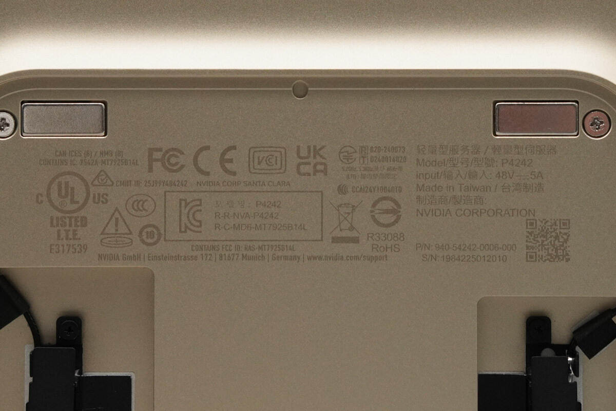
The NVIDIA DGX Spark lightweight server features a champagne-gold aluminum alloy chassis and a small-form-factor (SFF) design. It uses the NVIDIA GB10 superchip, with a 20-core CPU consisting of 10 Cortex-X925 cores and 10 Cortex-A725 cores.
The GPU has 6,144 CUDA cores, with FP4 performance reaching 1 PFLOPS, paired with 128 GB of unified memory, a memory bandwidth of 273 GB/s, using 16-channel LPDDR5X memory with a 256-bit interface. It has a ConnectX-7 network card with two QSFP ports, supporting 200 Gb/s network connectivity.
It uses an external power supply via a USB-C interface, with a PD 3.1 adapter rated at 48V/5A and providing 240 W output. The GB10 SoC has a thermal design power of 140 W, leaving 100 W for other system components. Below, we will take a closer look at the materials and build quality of the product.
Product Appearance
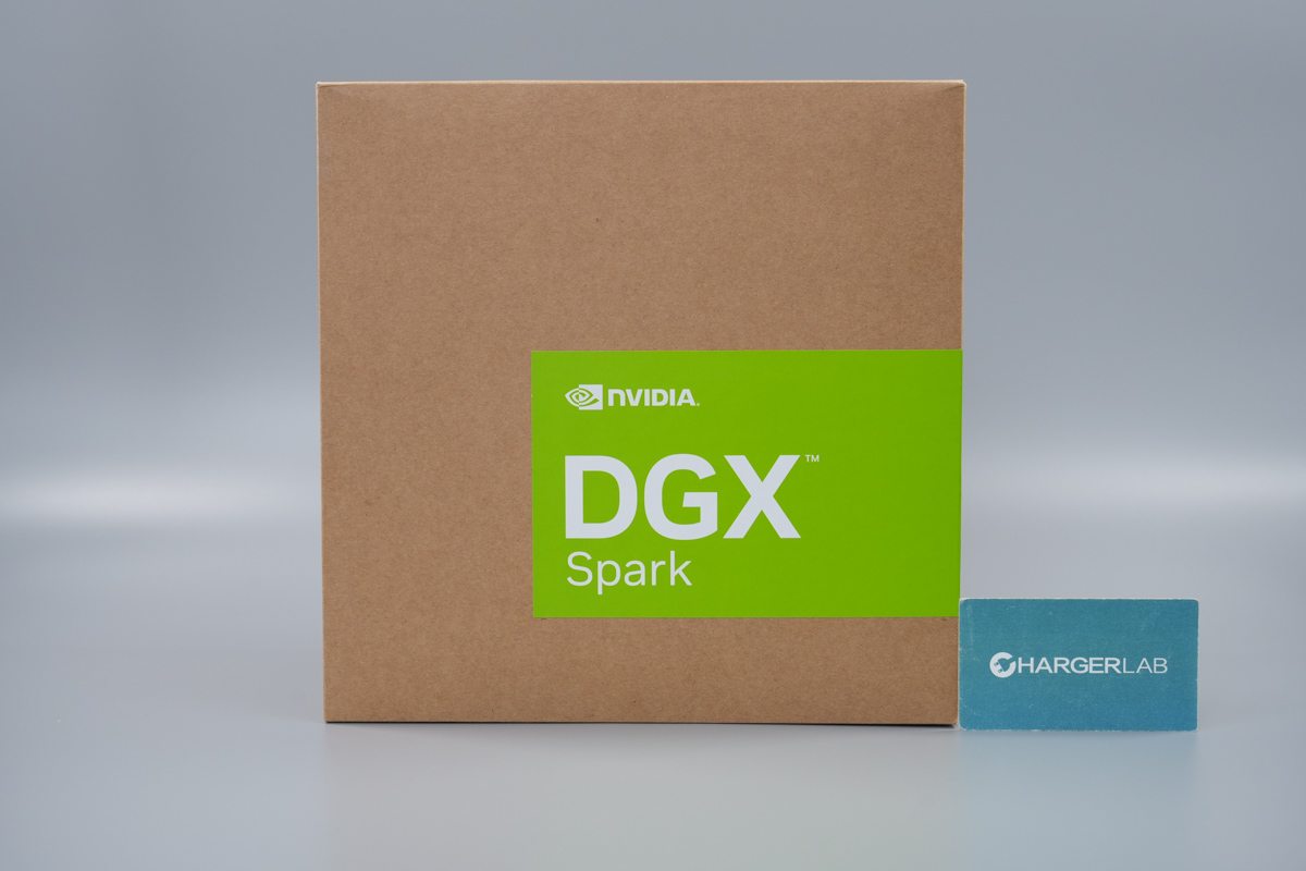
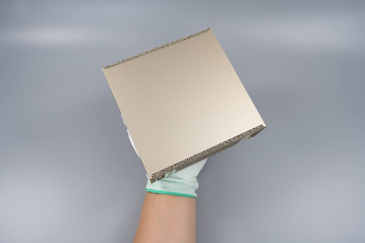
Packaged in a natural-colored cardboard box, printed with the NVIDIA, DGX, and Spark logos.
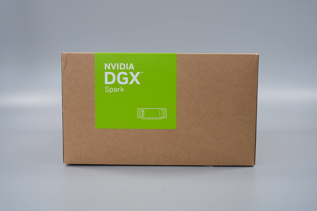
The sides also feature the NVIDIA, DGX, and Spark logos.
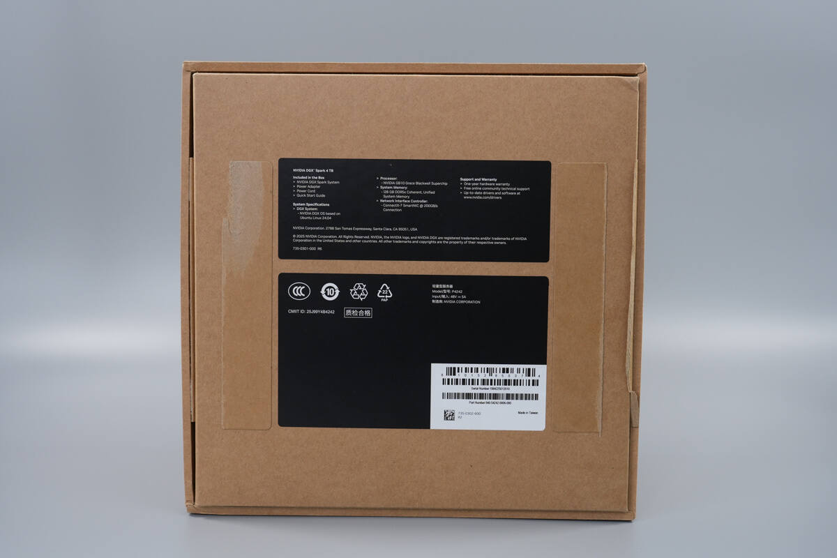
The rear has a tear-off seal and an information label attached.
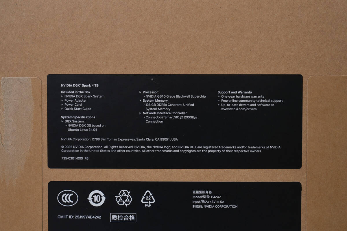
NVIDIA DGX Spark 4TB
The package contains the NVIDIA DGX Spark system, a power adapter, a power cord, and a quick start guide.
Processor
NVIDIA GB10 Grace Blackwell Superchip
System memory
128 GB DDR5X unified system memory
Network interface controller
ConnectX-7 smart network card
Includes a one-year hardware warranty
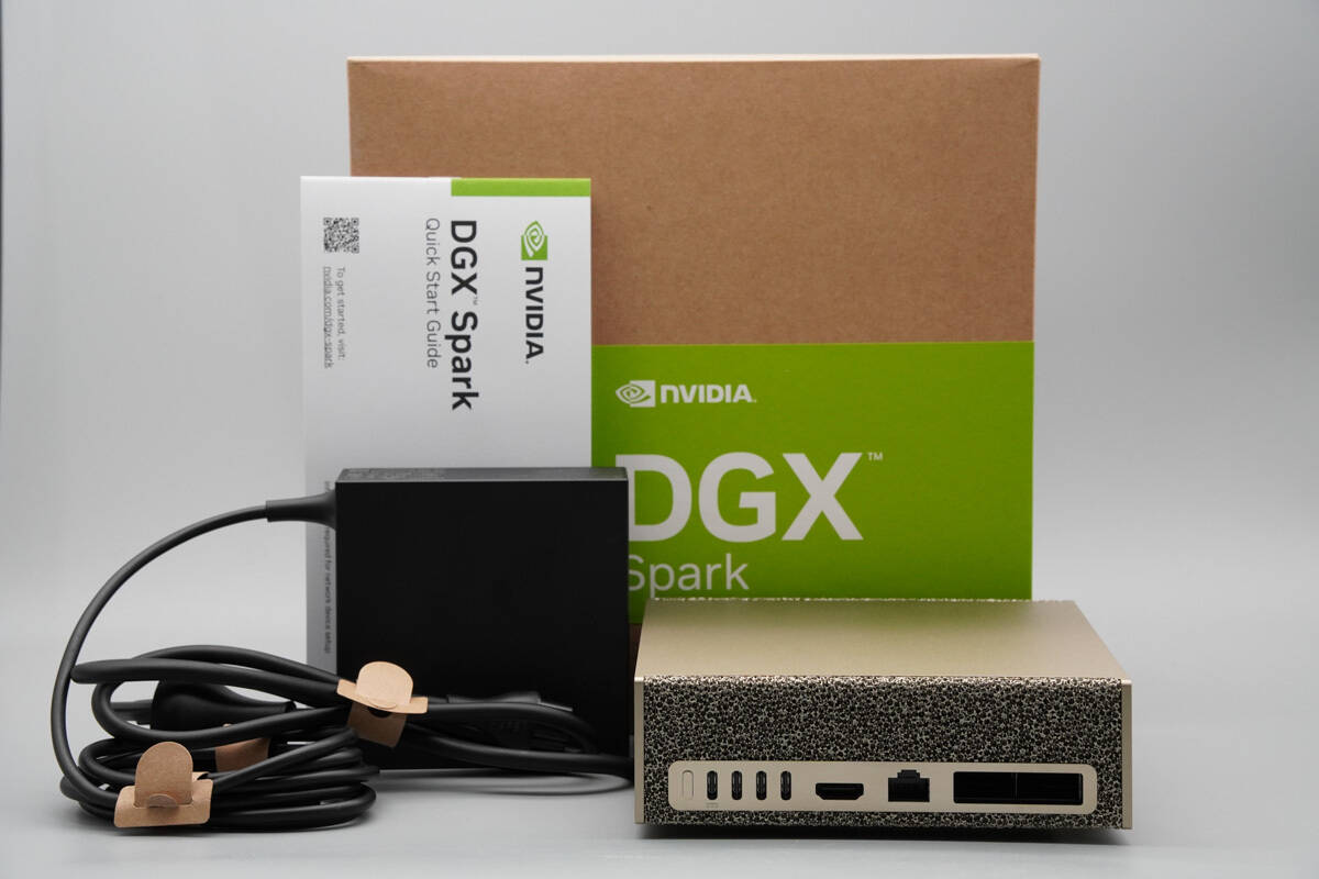
The package includes the NVIDIA DGX Spark, a PD 3.1 power adapter, a power cord, and a quick start guide.
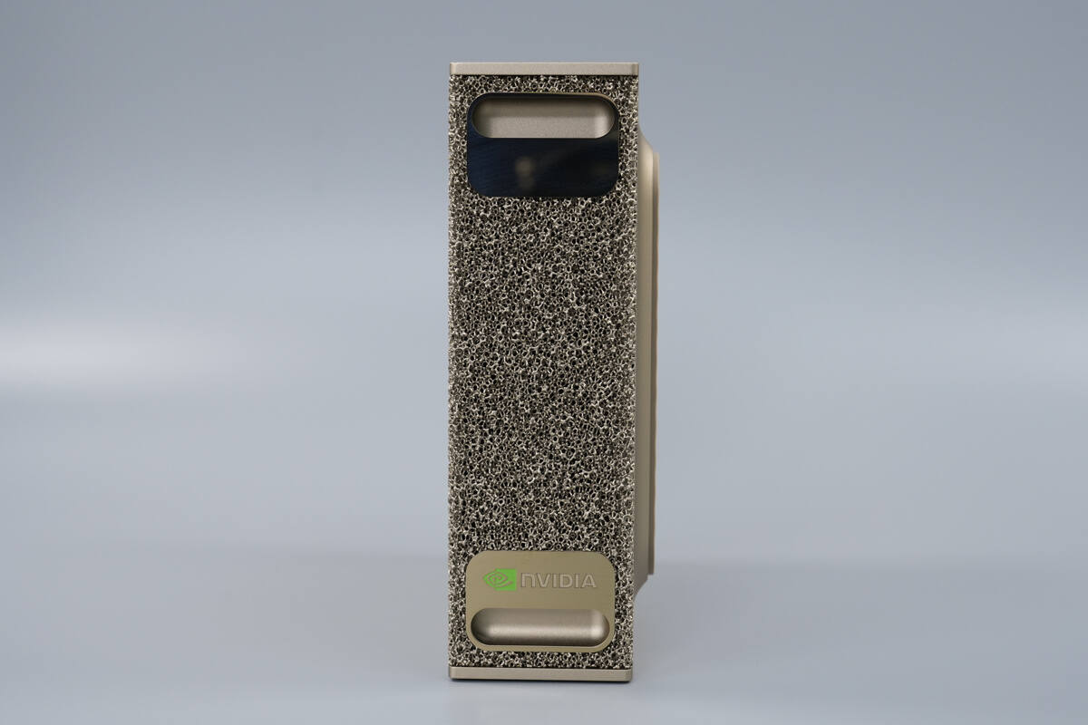
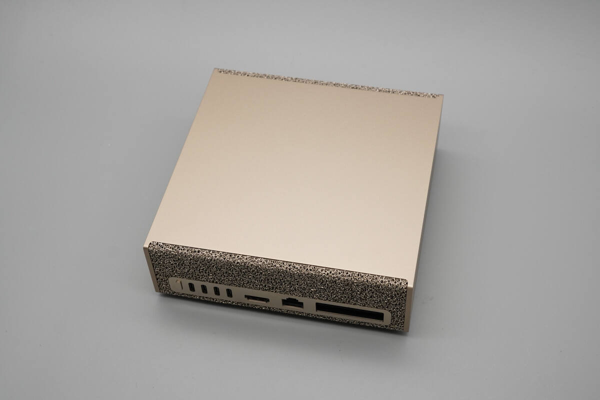
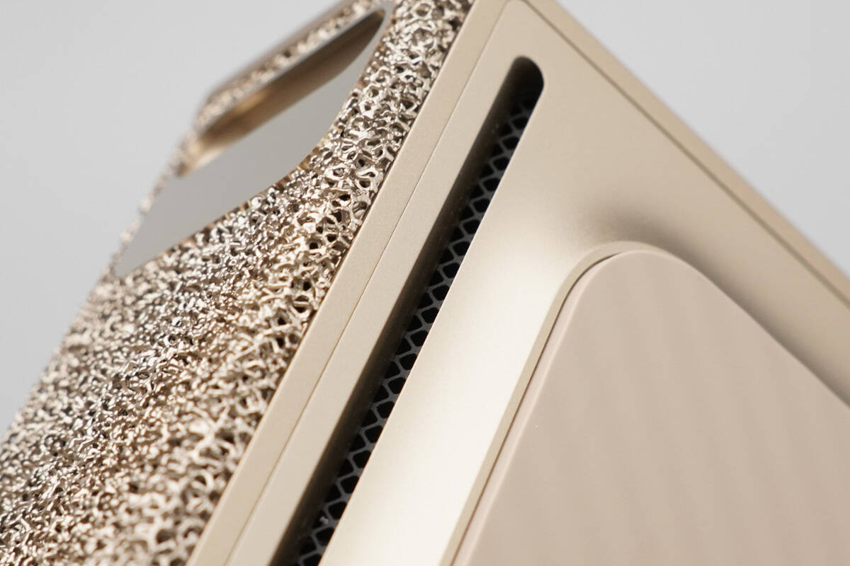
The front of the chassis features metal foam decoration, with air intakes located at the top and bottom.
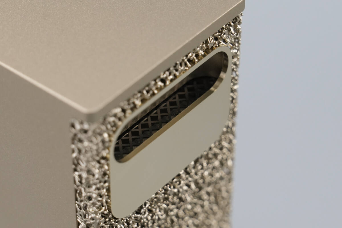
The air intakes are equipped with dust filters.
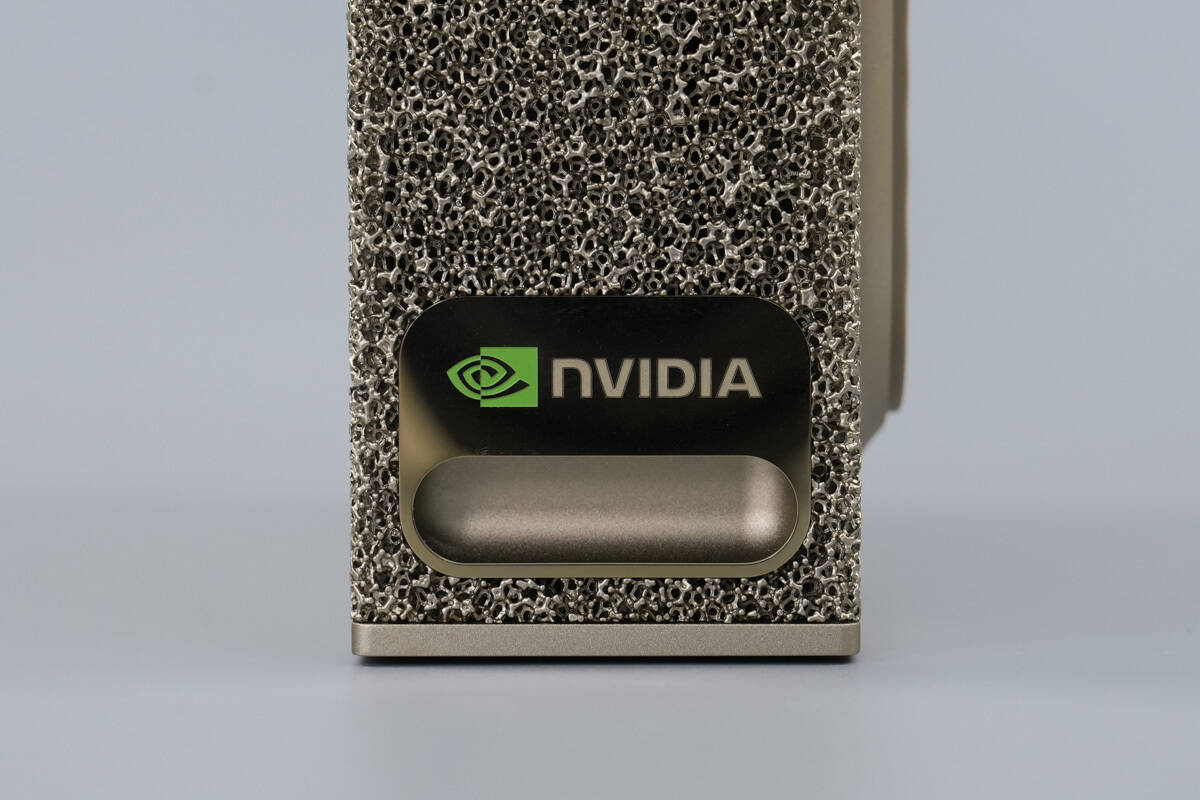
The lower air intake is marked with the NVIDIA logo.
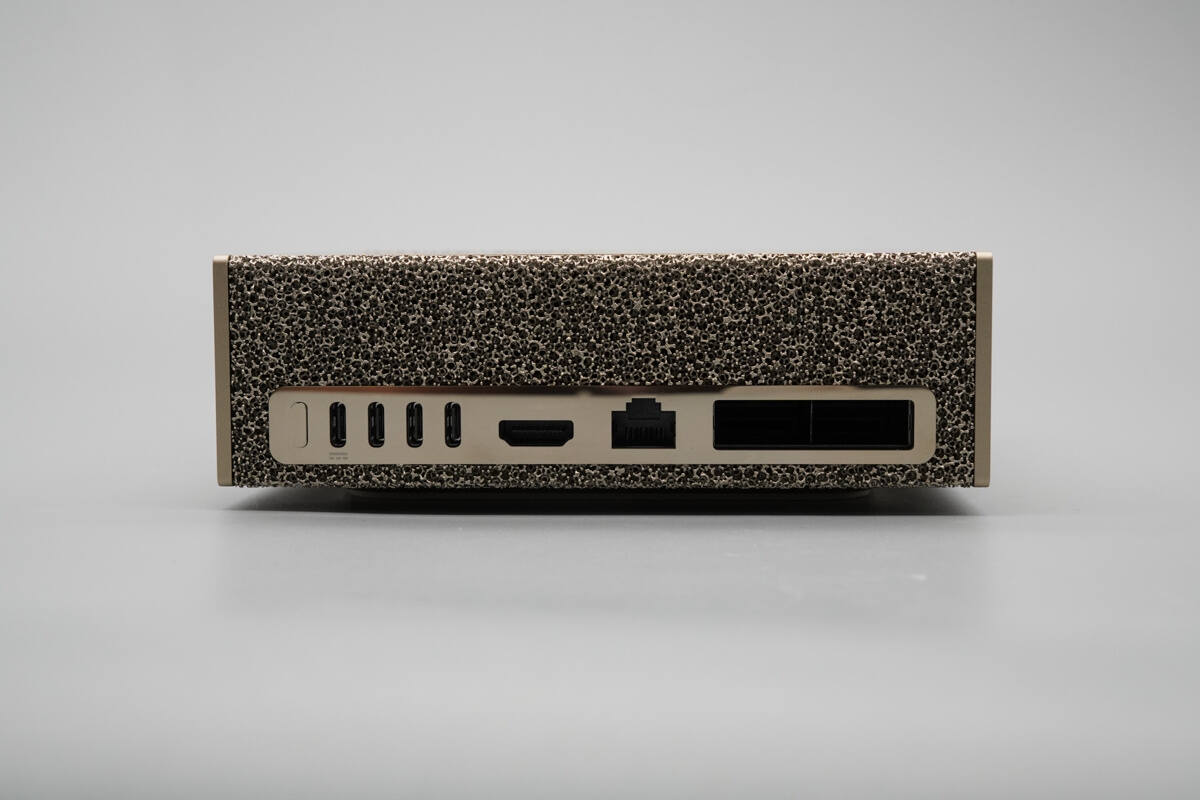
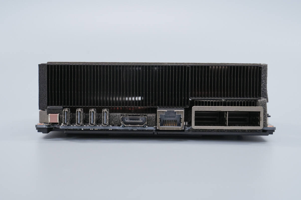
Overview of the rear ports.
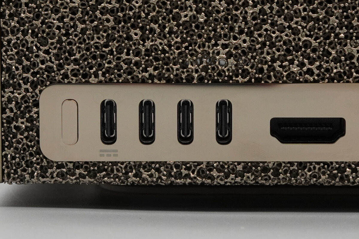
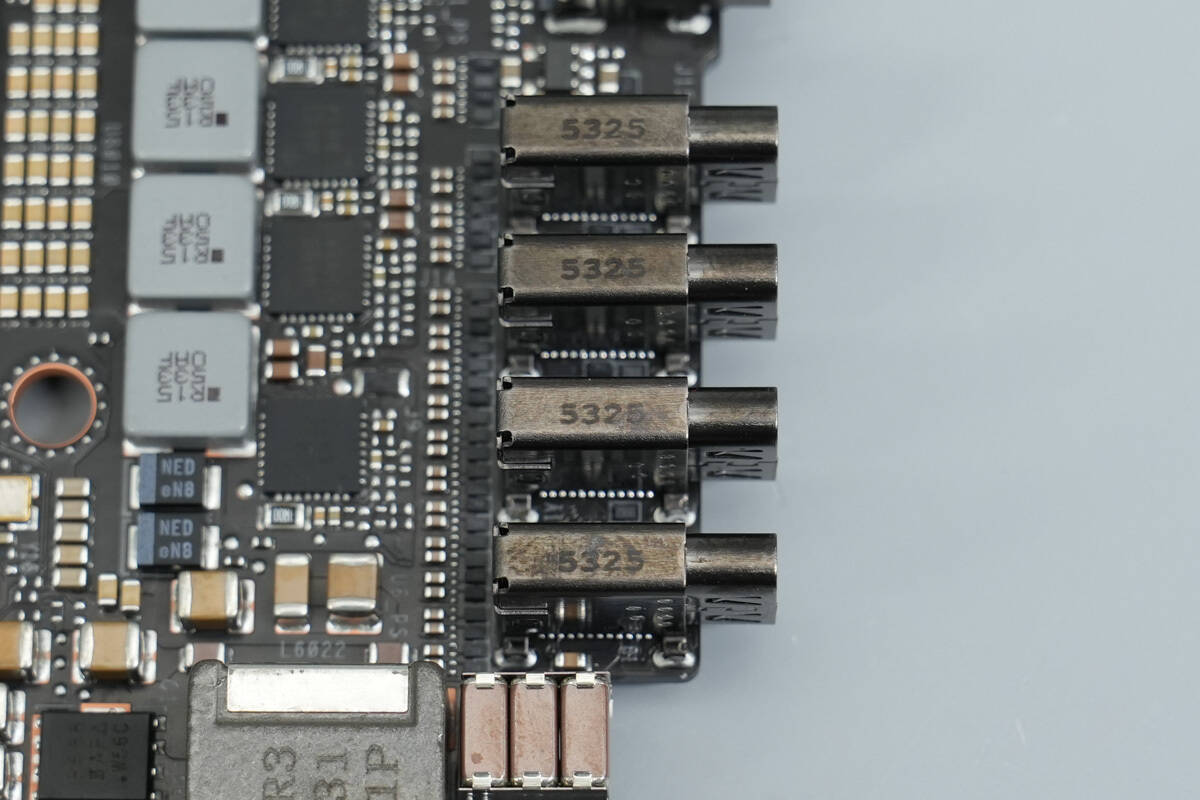
On the left side, there is a power button and four USB-C ports. The leftmost port is for power input, with a DC symbol printed below.
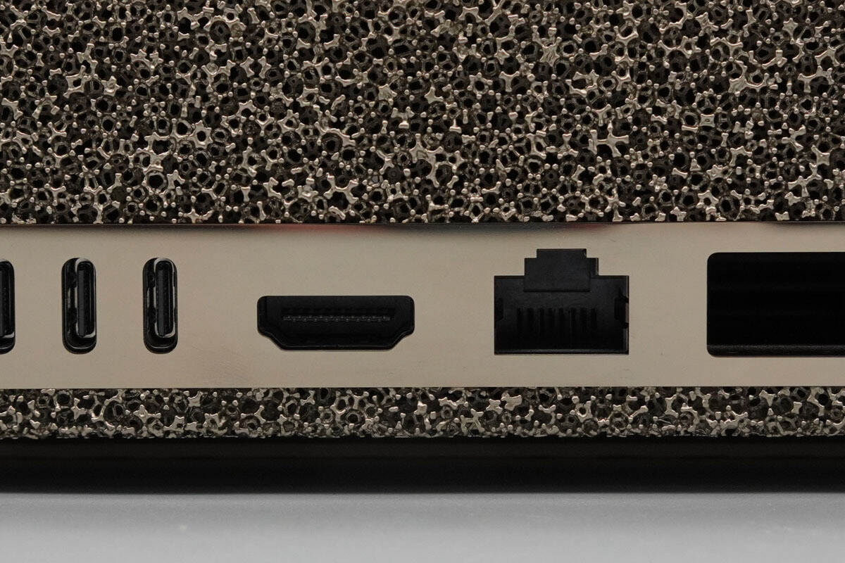
Close-up of the HDMI and 10G Ethernet ports.
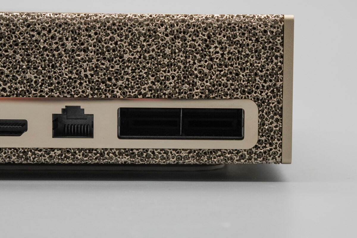
The right side has two QSFP ports.
The top of the chassis has a matte finish.
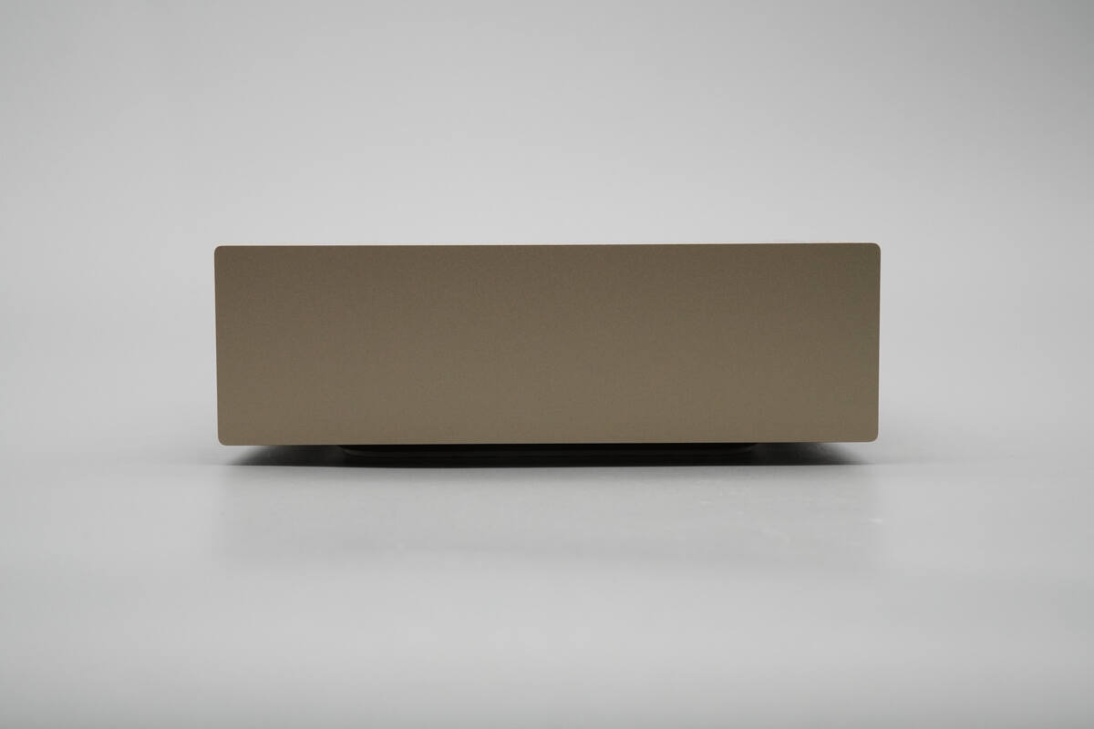
The sides of the chassis have a matte finish.
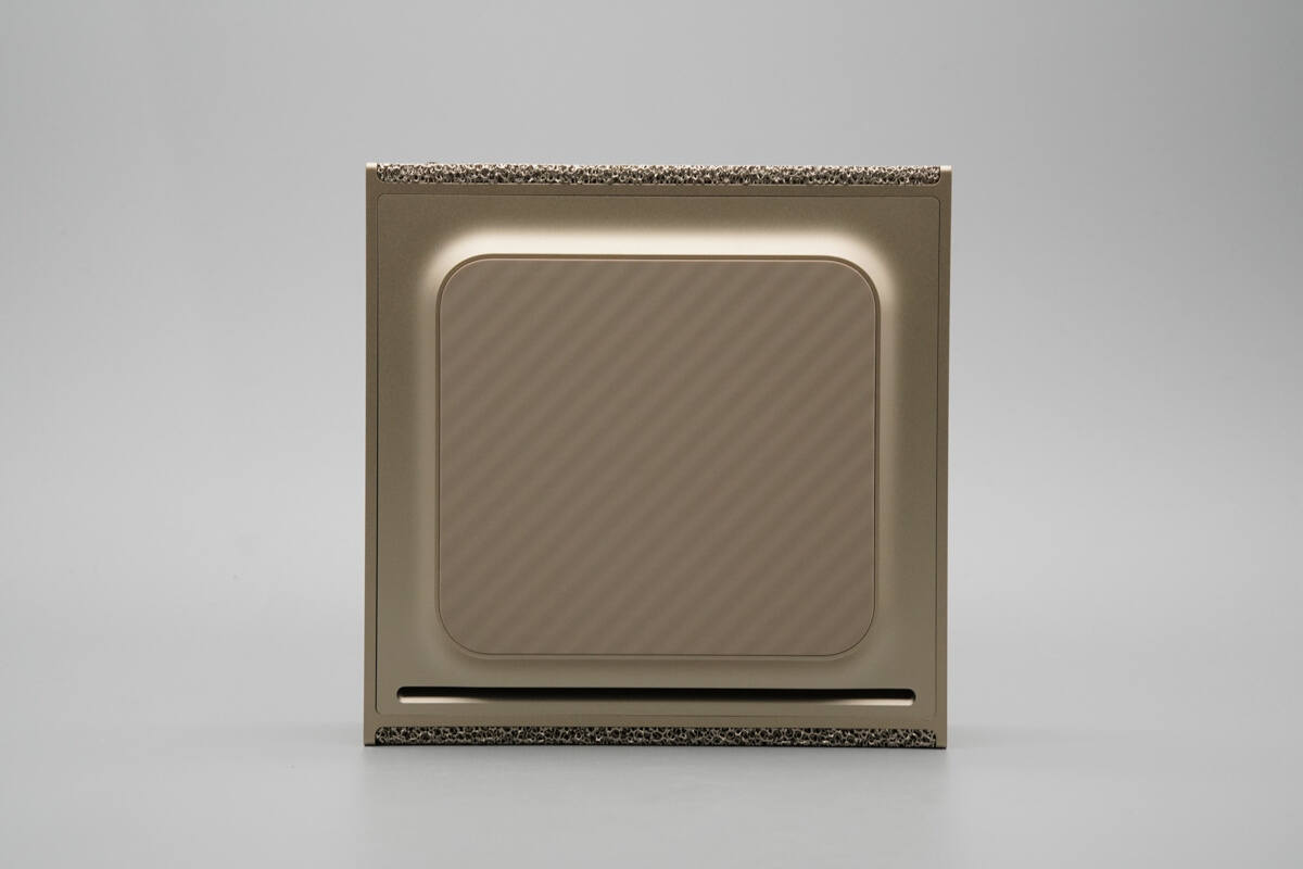
The bottom is equipped with a non-slip cover plate.
The bottom air intake is also equipped with a dust filter.
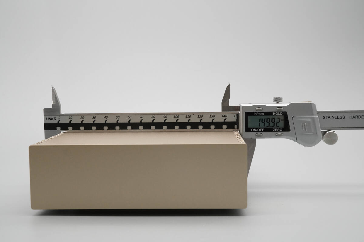
The length is about 150 mm (5.91 inches).
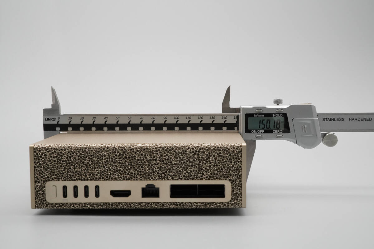
The width is about 150 mm (5.91 inches).
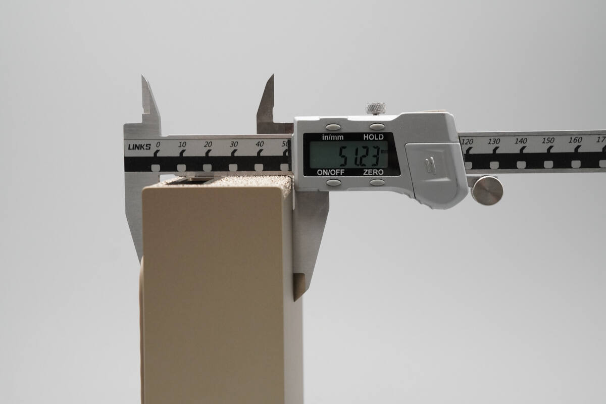
The thickness is about 51.2 mm (2.016 inches).
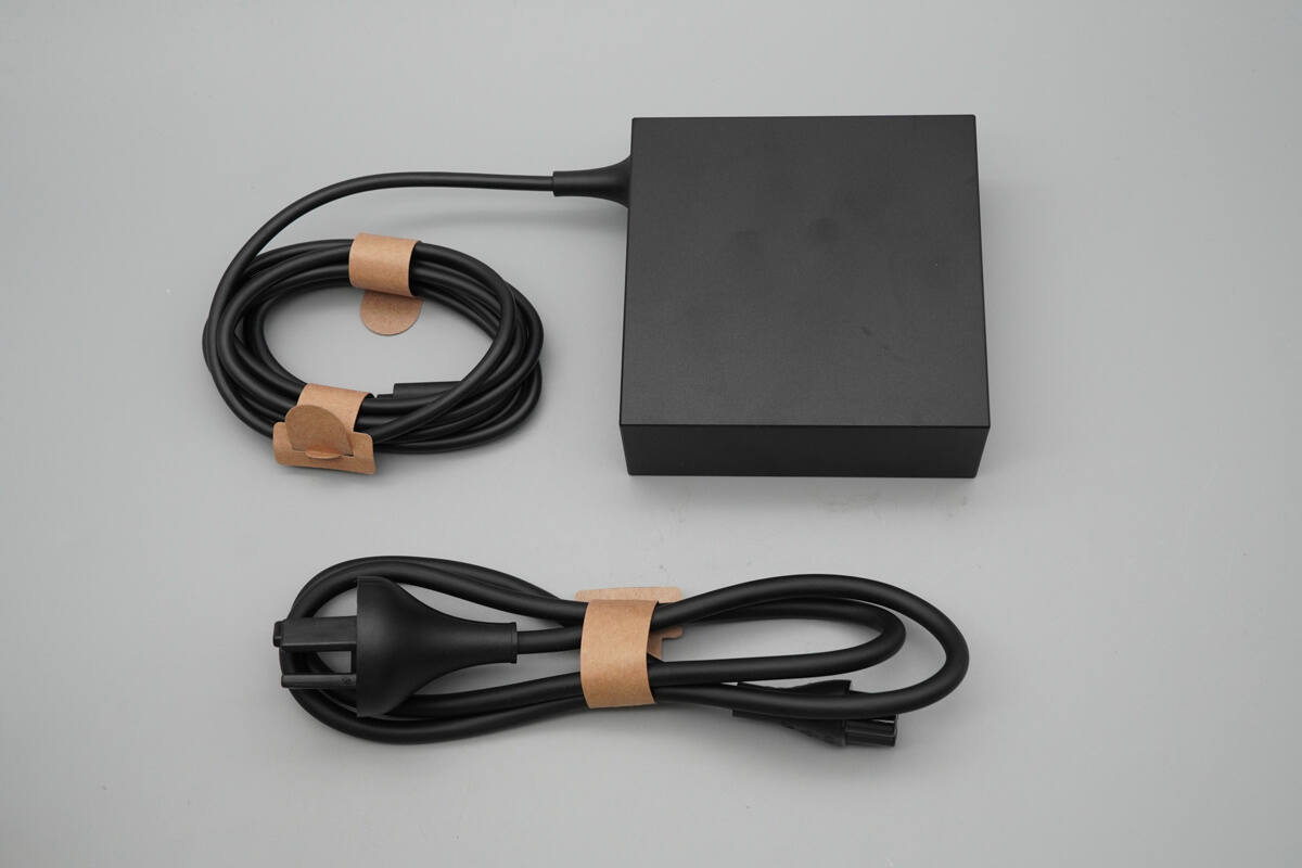
The power adapter and the included power cord are both secured with paper straps.
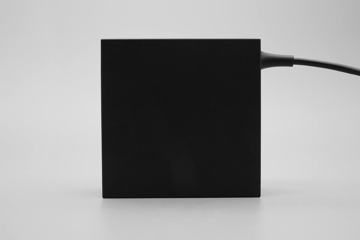
The power adapter has a rectangular block shape.
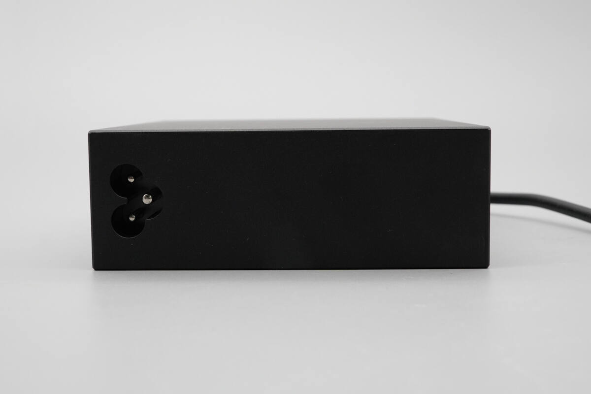
The input side features a cloverleaf connector.
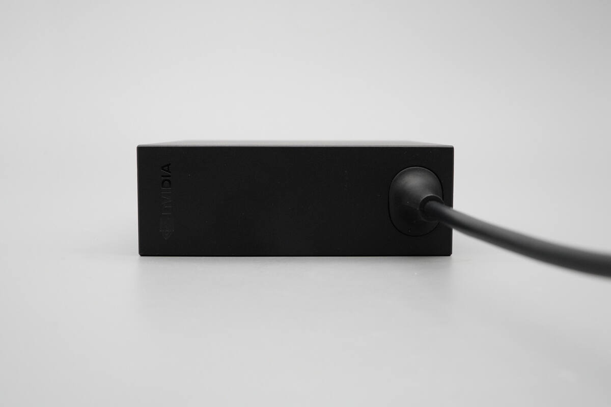
The output cable is integrated and features a rubber sleeve for bend protection.
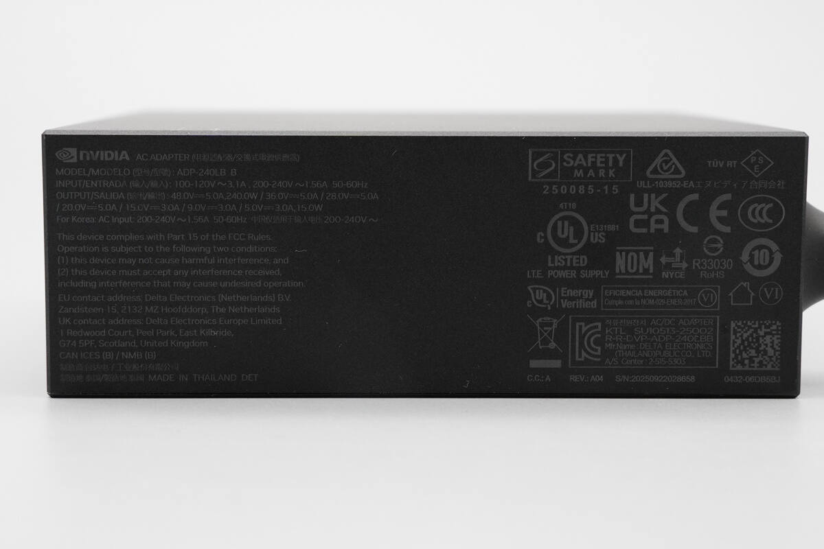
Model: ADP-240LB B
Input: 100–120V ~ 3.1A, 200–240V ~ 1.56A, 50–60Hz
Output: 48V⎓5A, 240W / 36V⎓5A / 28V⎓5A / 20V⎓5A / 15V⎓3A / 9V⎓3A / 5V⎓3A, 15W
Manufacturer: Delta Electronics, Inc.
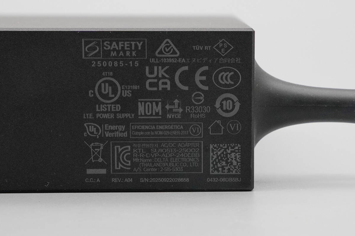
Close-up of multiple safety certification marks on the right side.
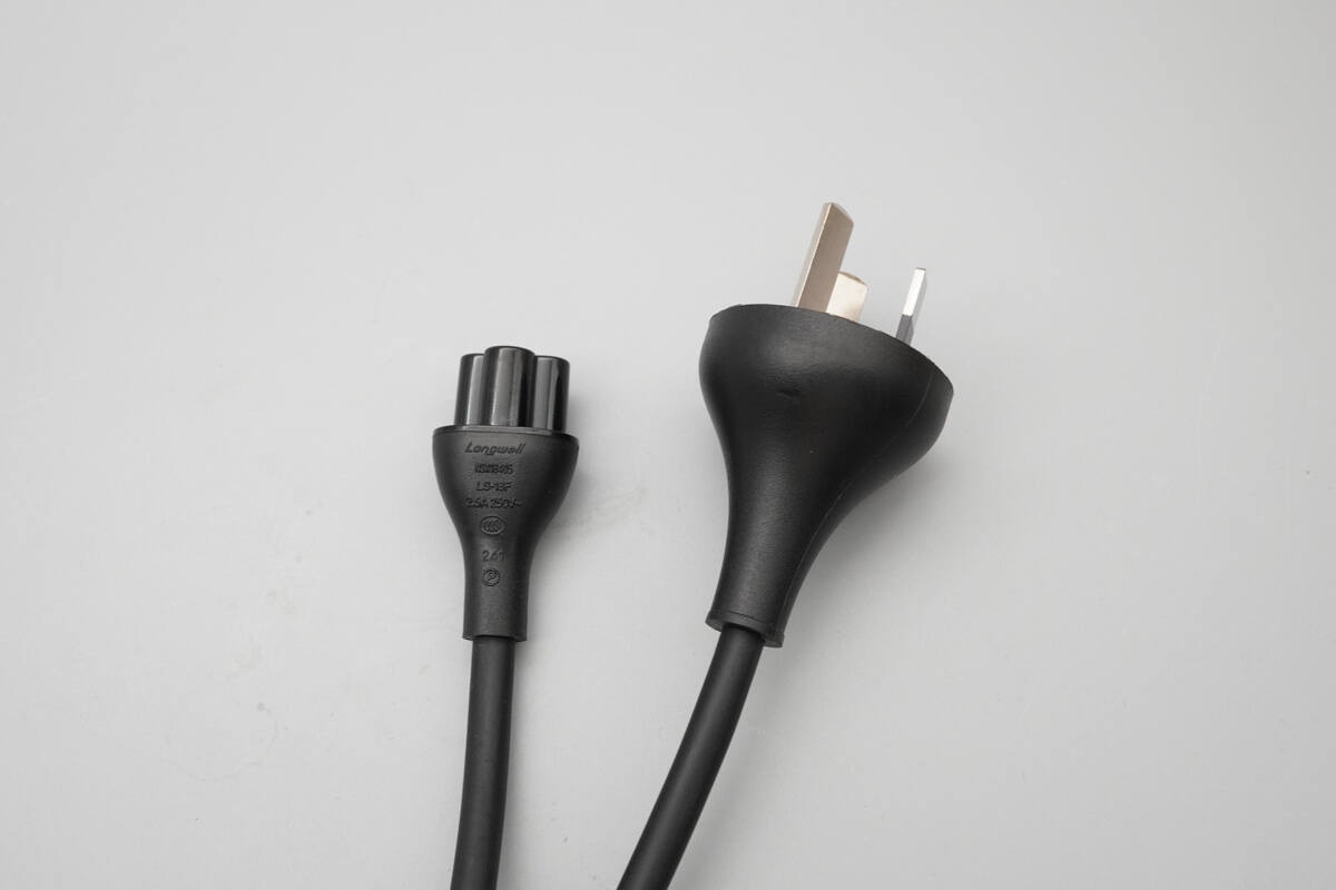
The power cord is equipped with a three-prong plug.
That's how big it is in the hand.
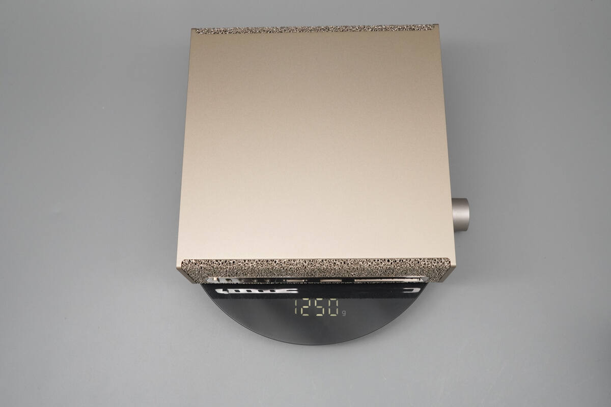
The weight is about 1250 g (44.092 oz).
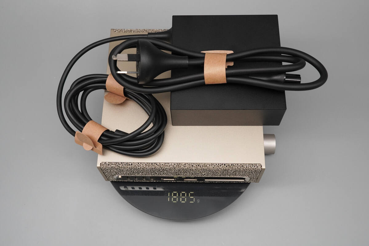
The combined weight of the power adapter and power cord is about 1885 g (66.49 oz).
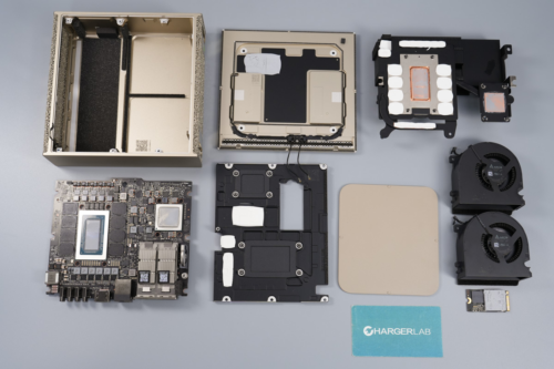
Teardown
Next, let's take it apart to see its internal components and structure.
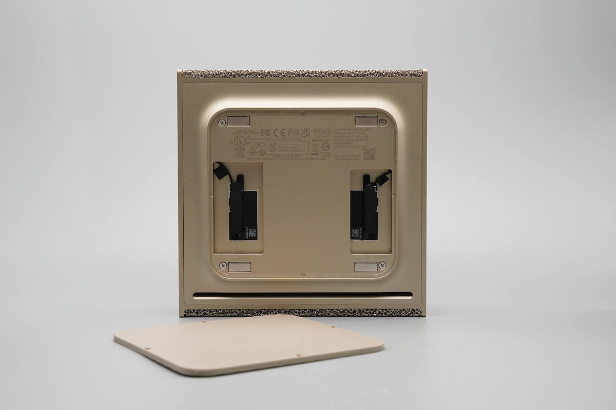
First, remove the non-slip cover plate from the bottom.
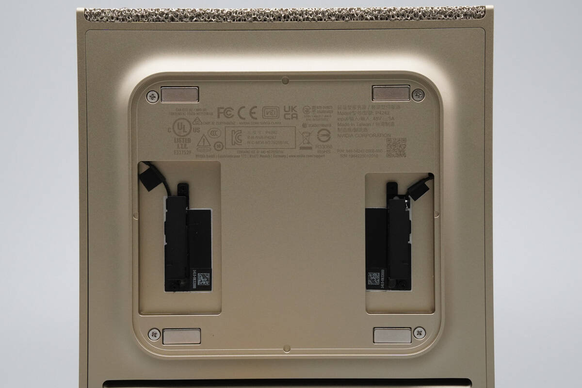
Inside the cover plate, there are mounting screws, a WiFi antenna, and printed product information.
Lightweight server
Model: P4242
Input: 48V⎓5A
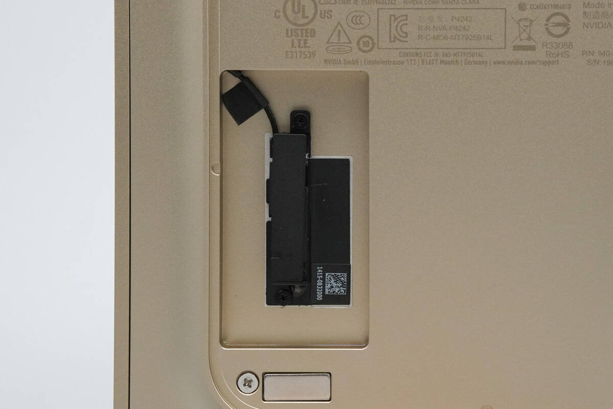
The WiFi antenna module is secured with screws.
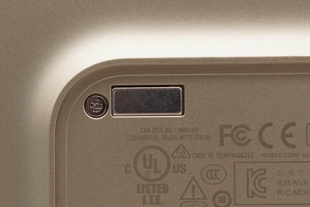
Close-up of the screws used to secure the rear cover and the magnets that hold the cover plate.
Remove the rear cover. The aluminum alloy base plate is secured to the chassis with screws along both side edges.
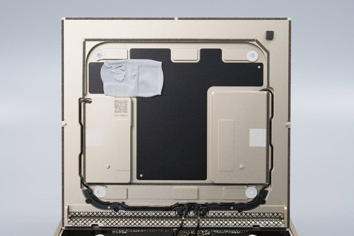
Inside the rear cover, a graphite thermal pad is attached, with a thermal pad positioned corresponding to the SSD location.
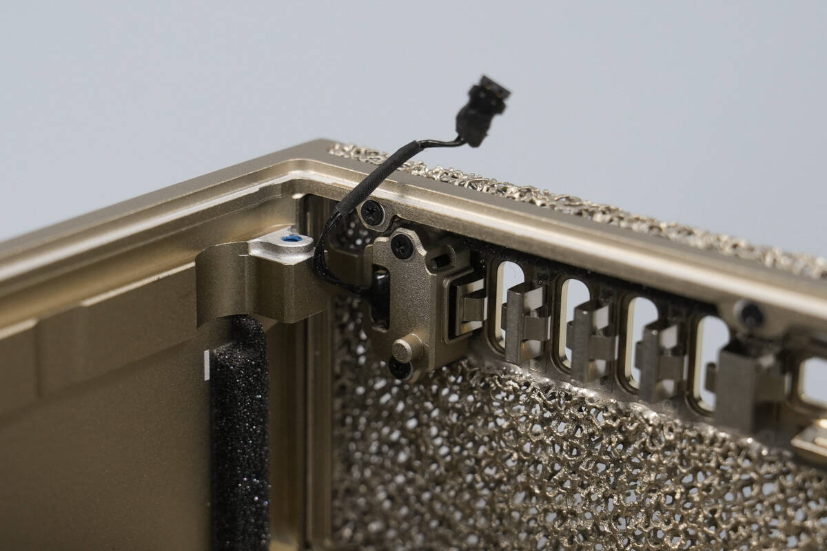
The WiFi antenna is connected via a shielded feed cable.
The antenna is secured with a retaining plate.
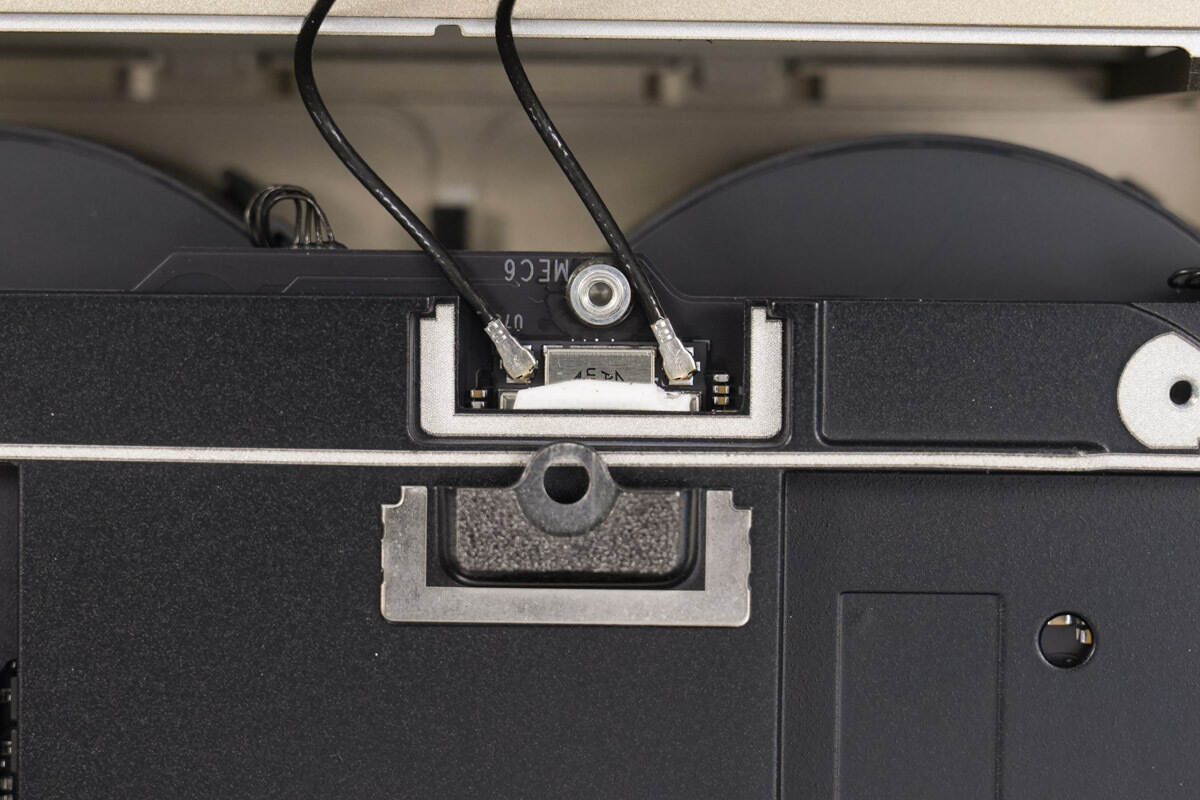
Remove the retaining plate to reveal the internal connector.
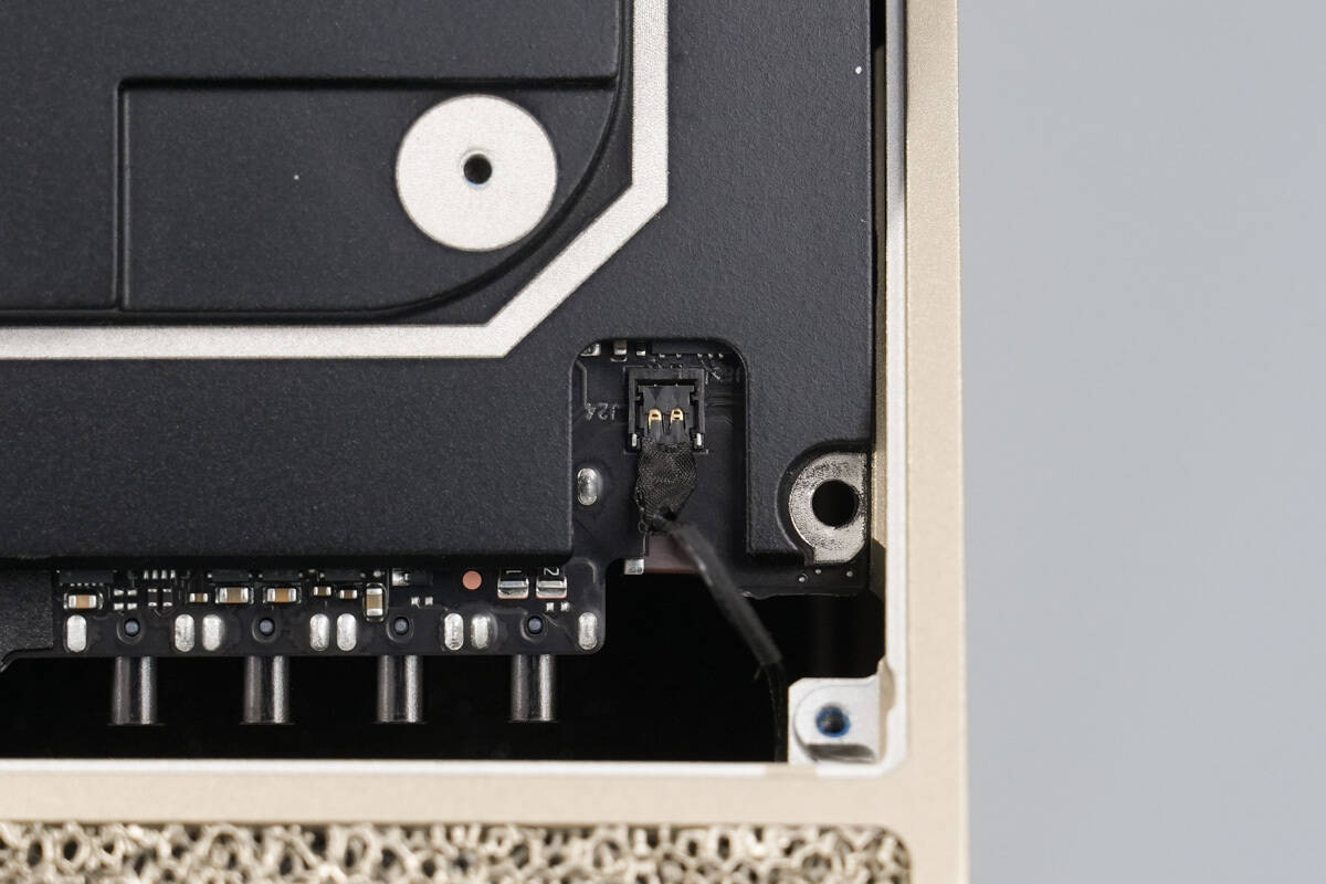
The power button is connected via a connector.
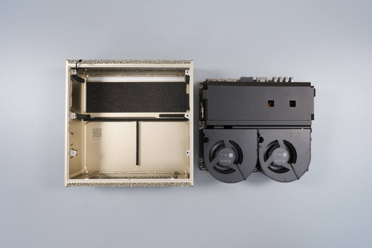
Remove the internal module.
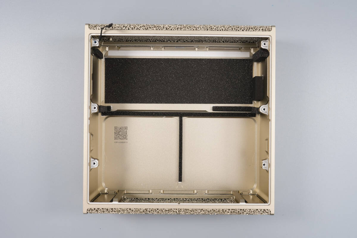
The chassis is made of aluminum alloy using CNC machining, with sealed foam inside.
The power button is connected via a ribbon cable and secured with a retaining plate.
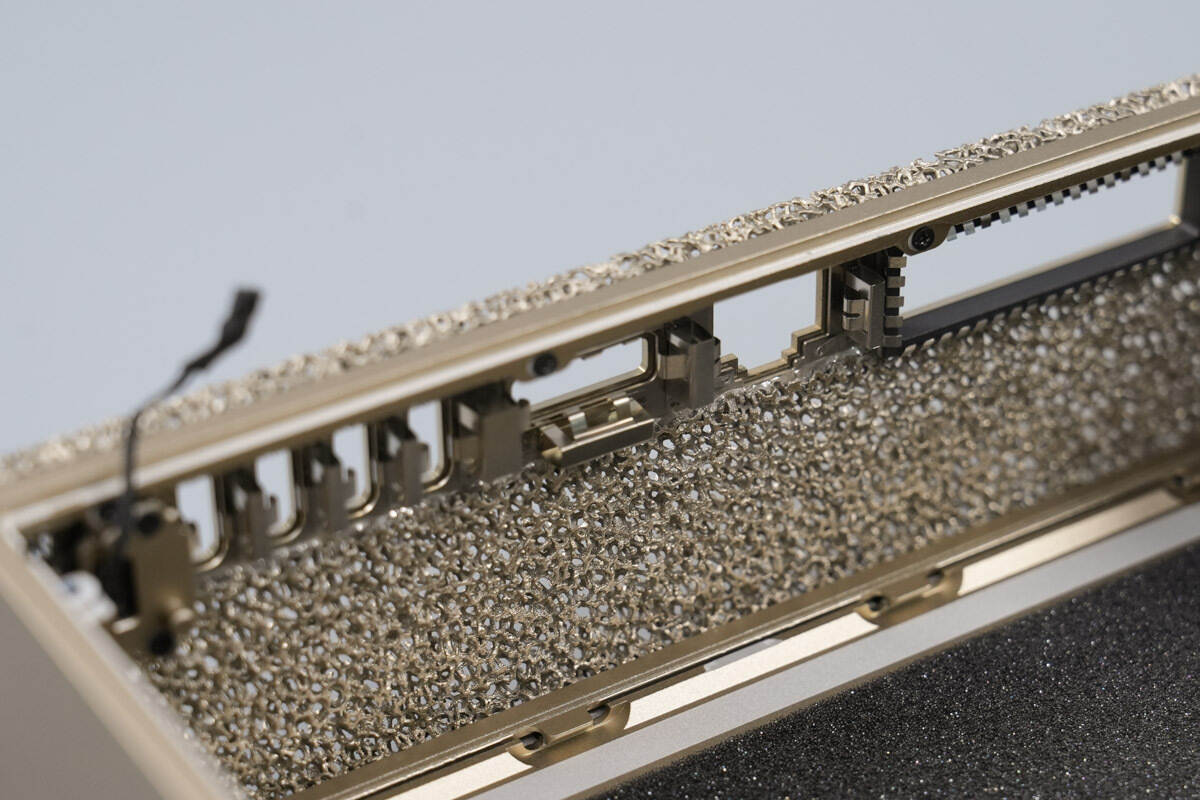
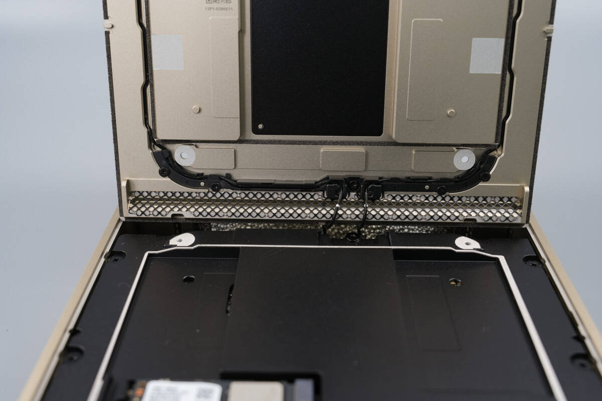
The chassis has spring shields corresponding to the ports.
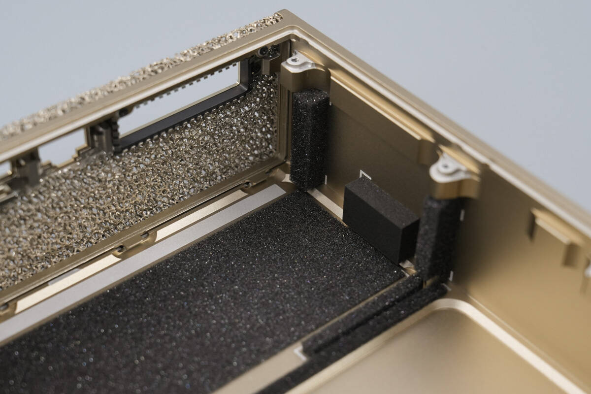
Foam is attached inside to seal gaps and prevent airflow backflow, which could affect cooling performance.
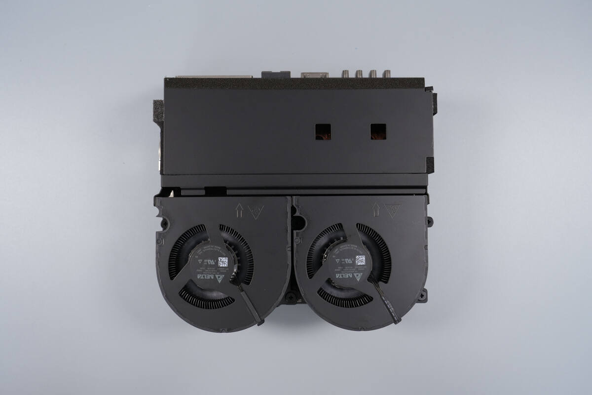
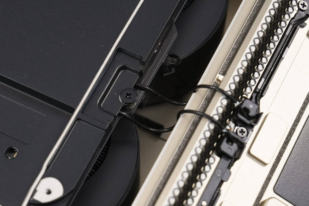
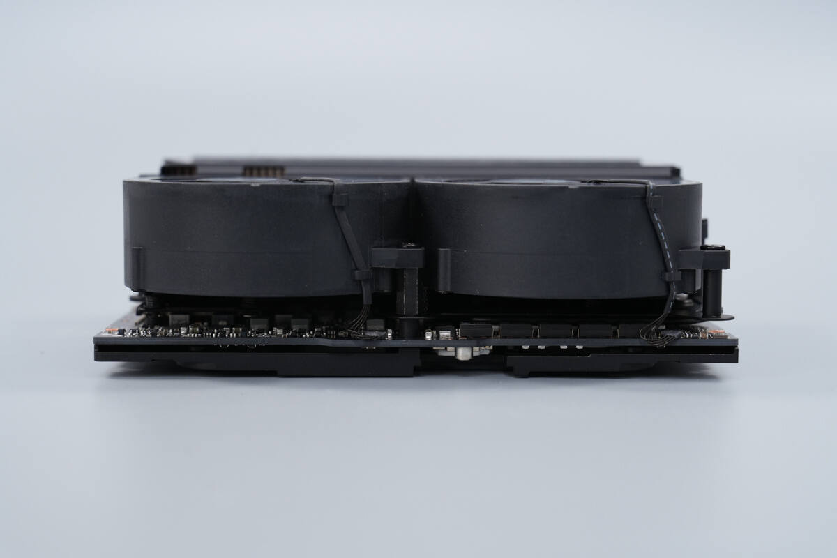
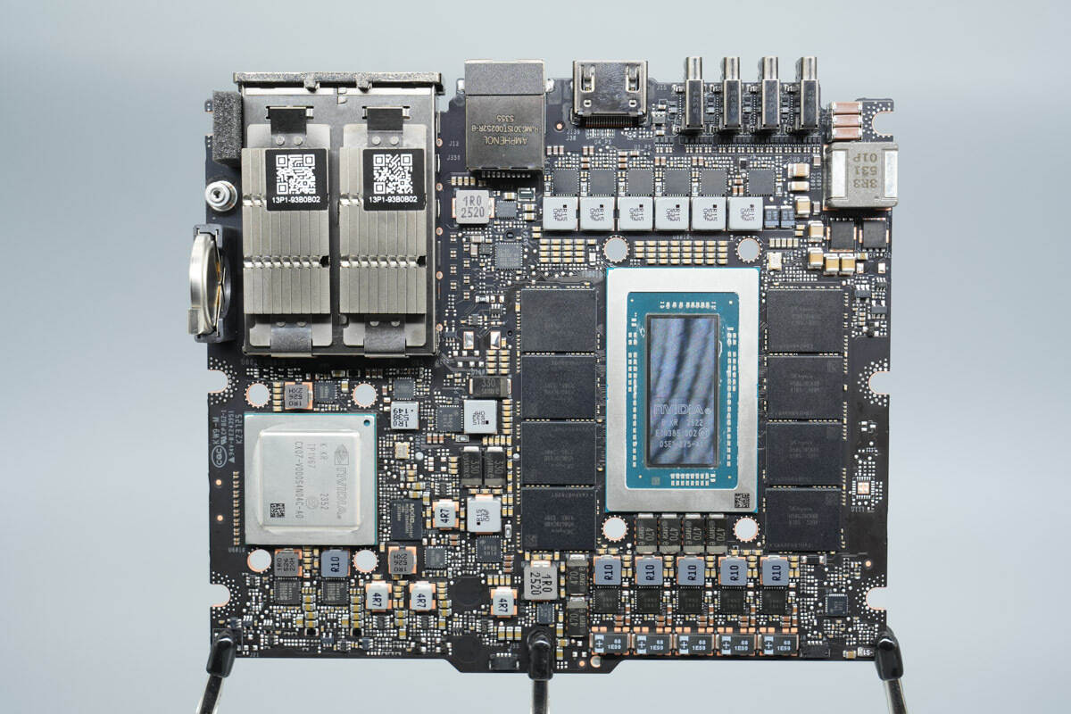
The cooling fans and heat dissipation module are mounted above the PCBA module.
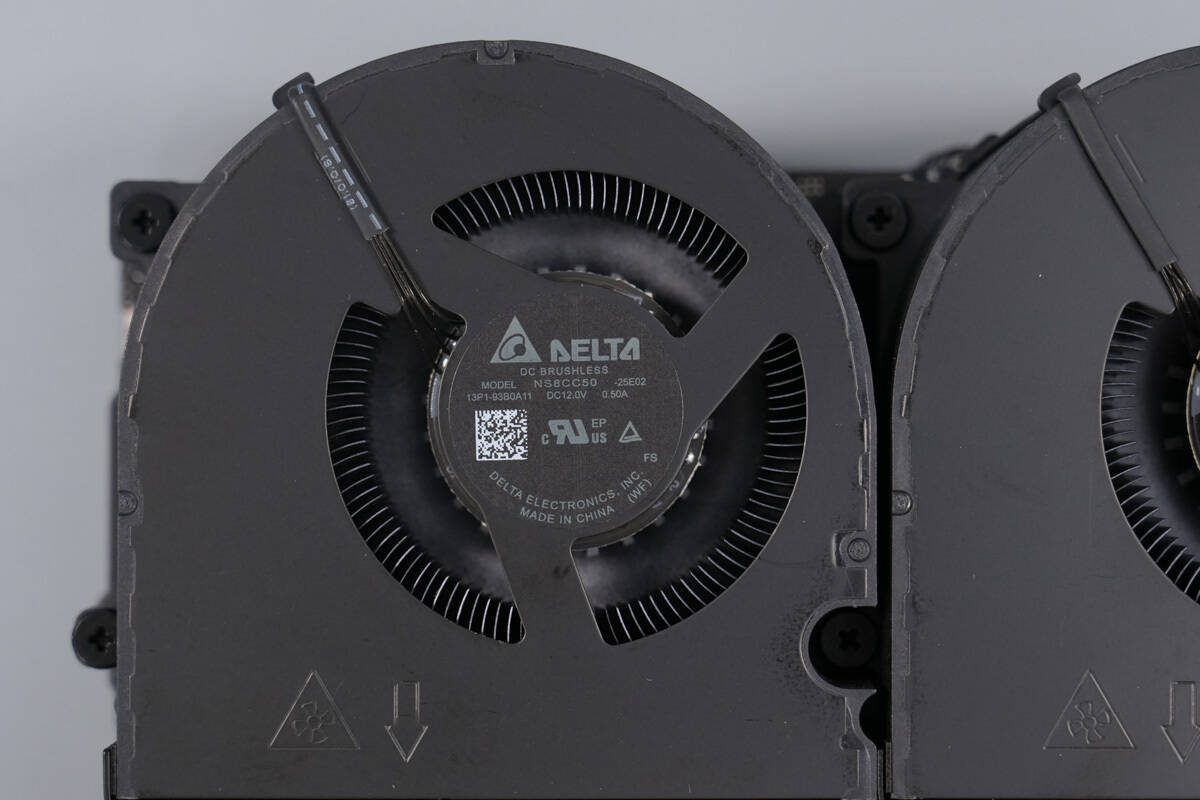
The cooling fan is from Delta, model NS8CC50, rated at 12V 0.5A.
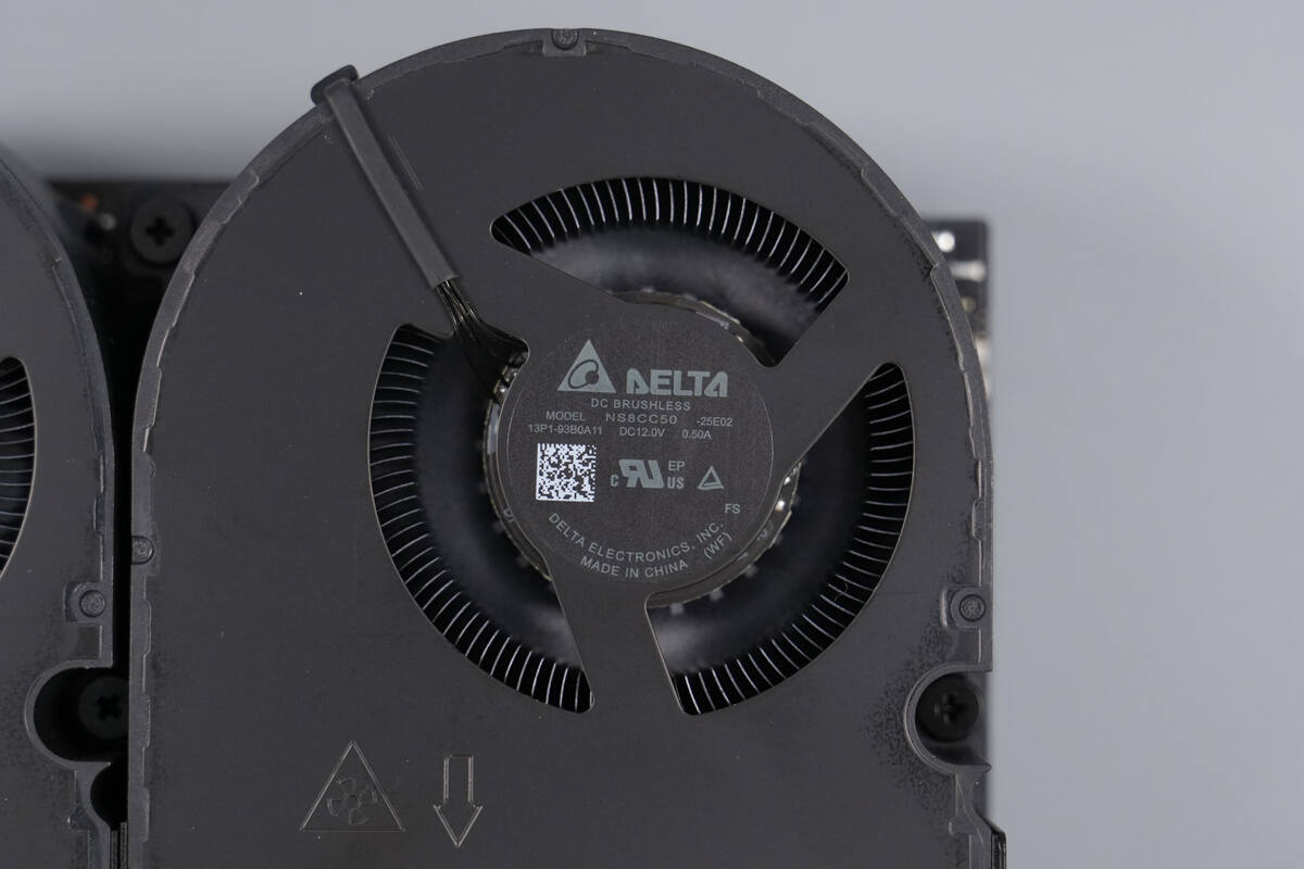
The other fan has the same model.
Overview of the exhaust heat sink fins; the housing corresponding to the QSFP connectors also has heat sink fins to dissipate heat using airflow.
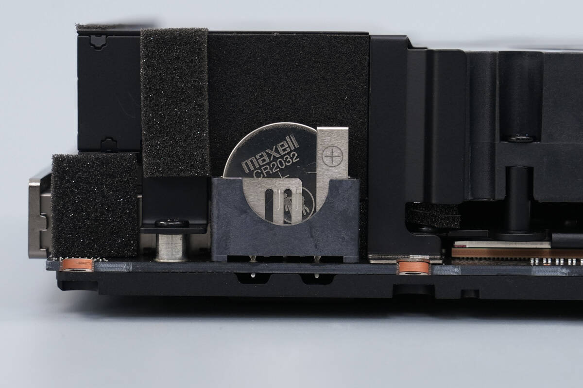
The clock battery is vertically mounted in a battery holder for easy replacement. The battery model is CR2032.
The cooling fans are connected via sockets.
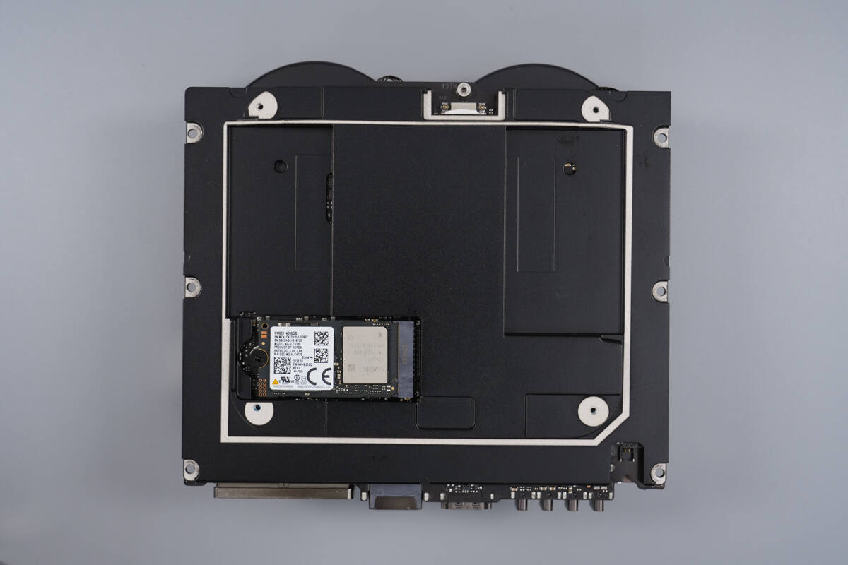
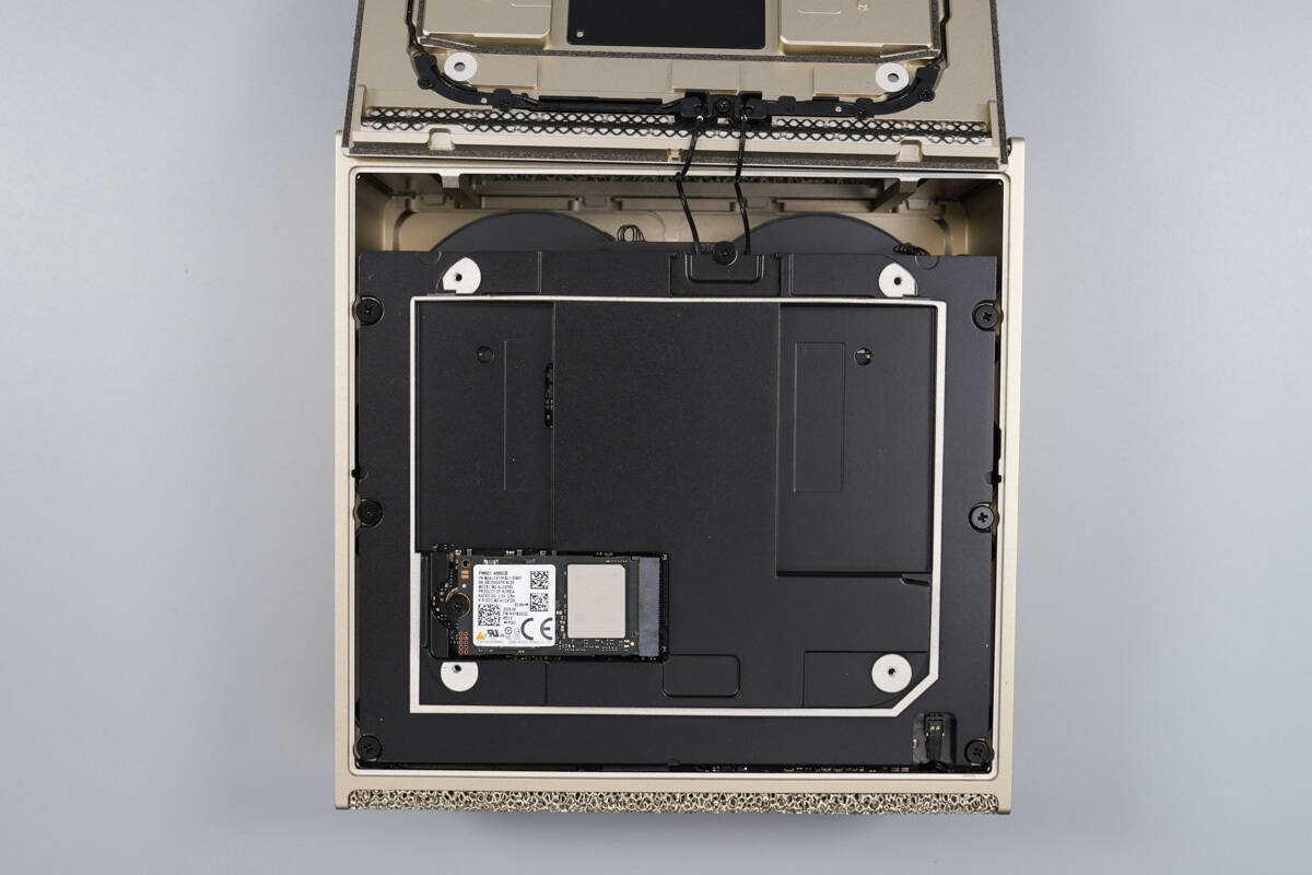
The aluminum alloy base plate has a cutout to secure a 2242-size SSD.
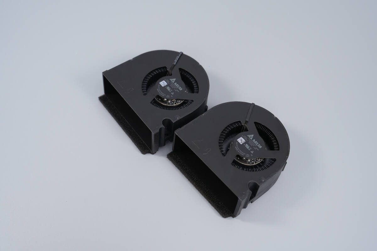
Remove the cooling fans.
The heat dissipation module has standoff screws to secure the fans.
The heat dissipation module is secured with screws.
Remove the heat dissipation module.
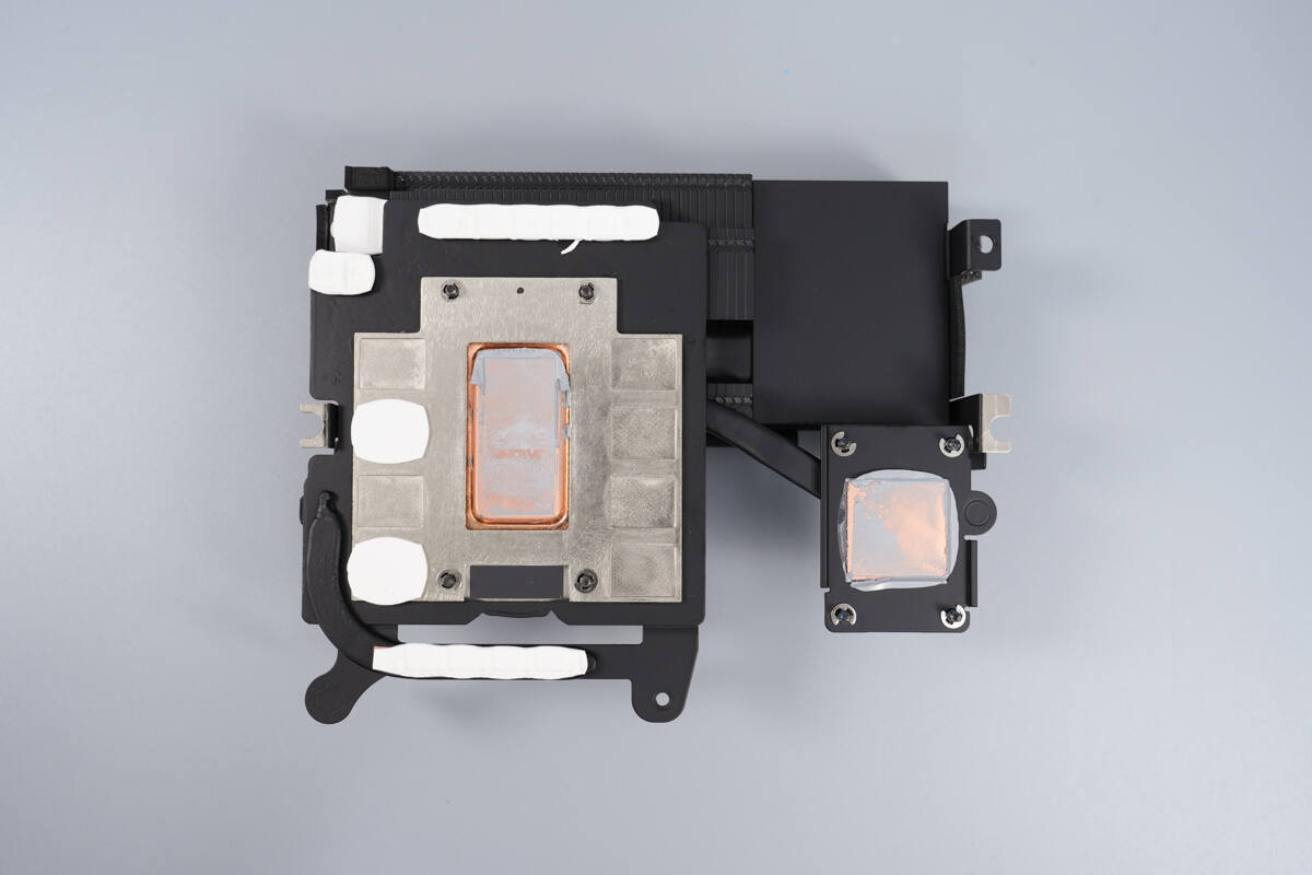
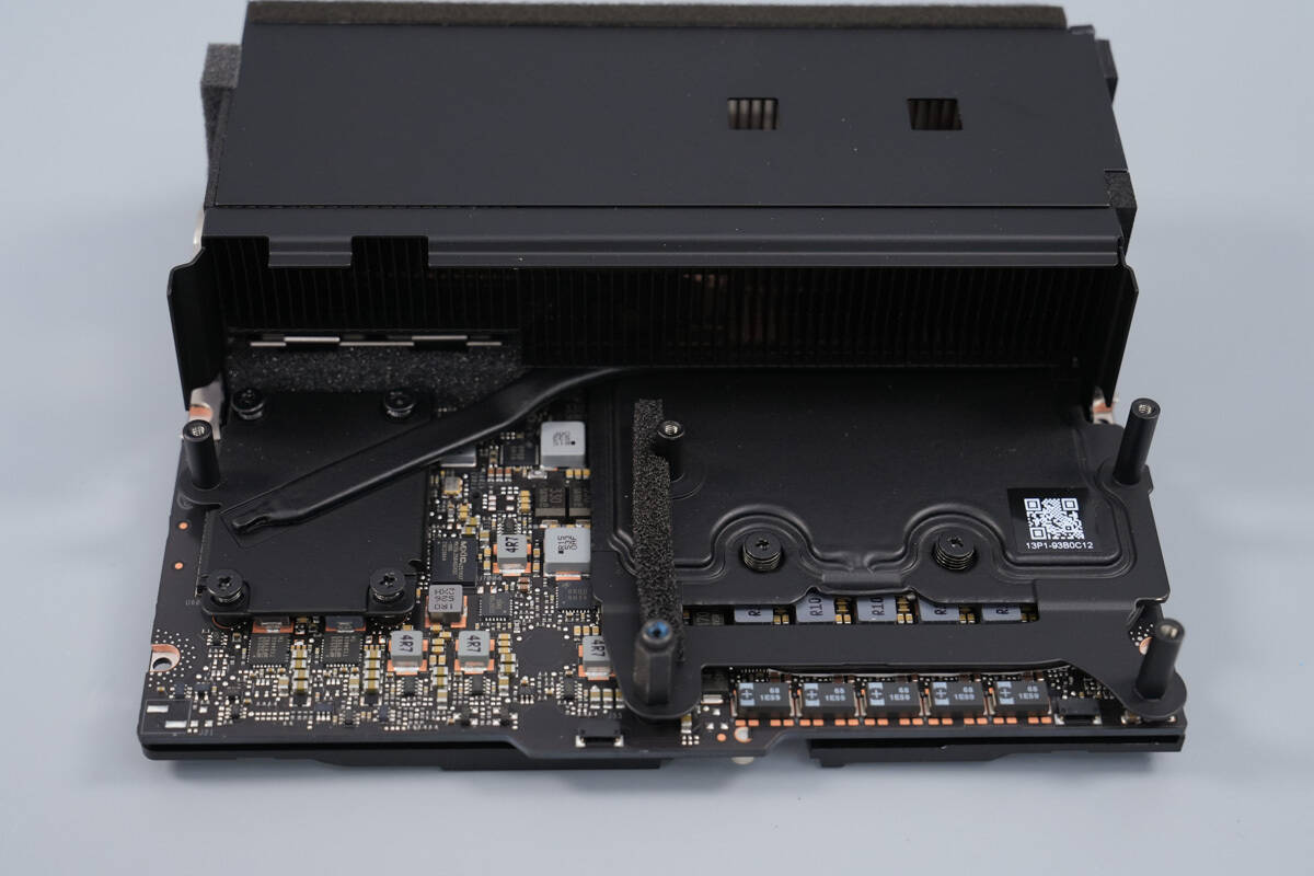
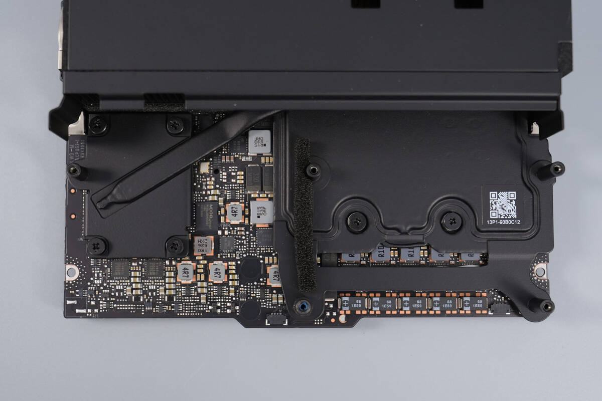
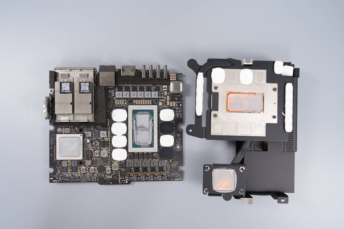
The heat dissipation module has a heat spreader positioned over the GB10 chip. Thermal pads are applied to the memory chips, buck inductors, and buck MOSFETs for heat dissipation. The DrMOS components feature heat pipes with thermal pads to enhance cooling. The network card chip also uses a heat pipe for thermal management.
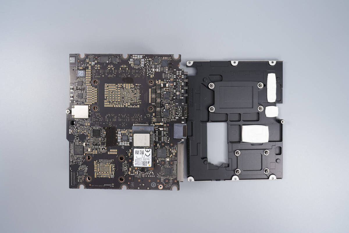
Next, remove the aluminum alloy base plate from the back of the PCBA module.
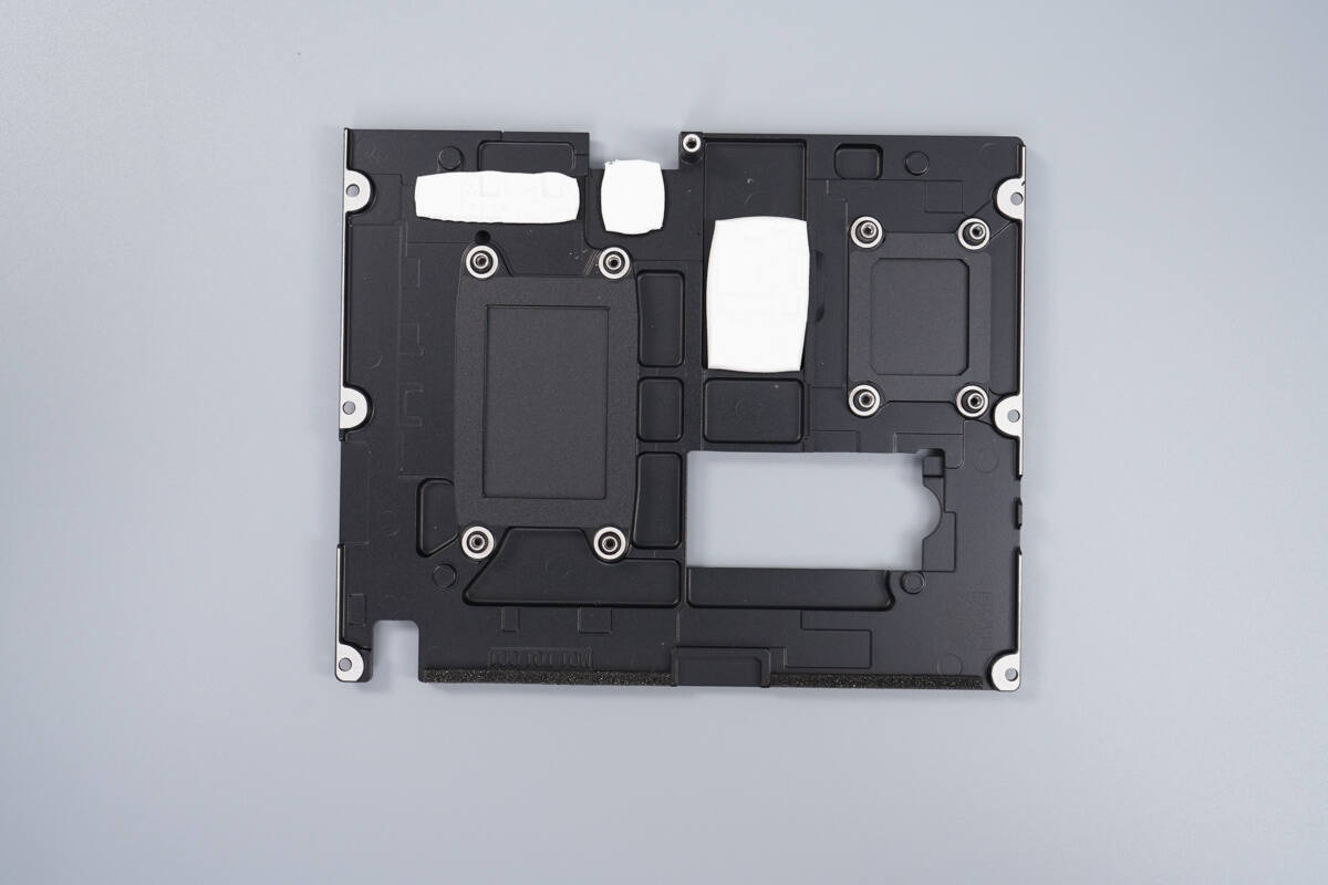
Thermal pads are applied on the base plate at the locations corresponding to the wireless network card and DrMOS components to enhance heat dissipation.
The back of the PCBA module is equipped with an SSD.
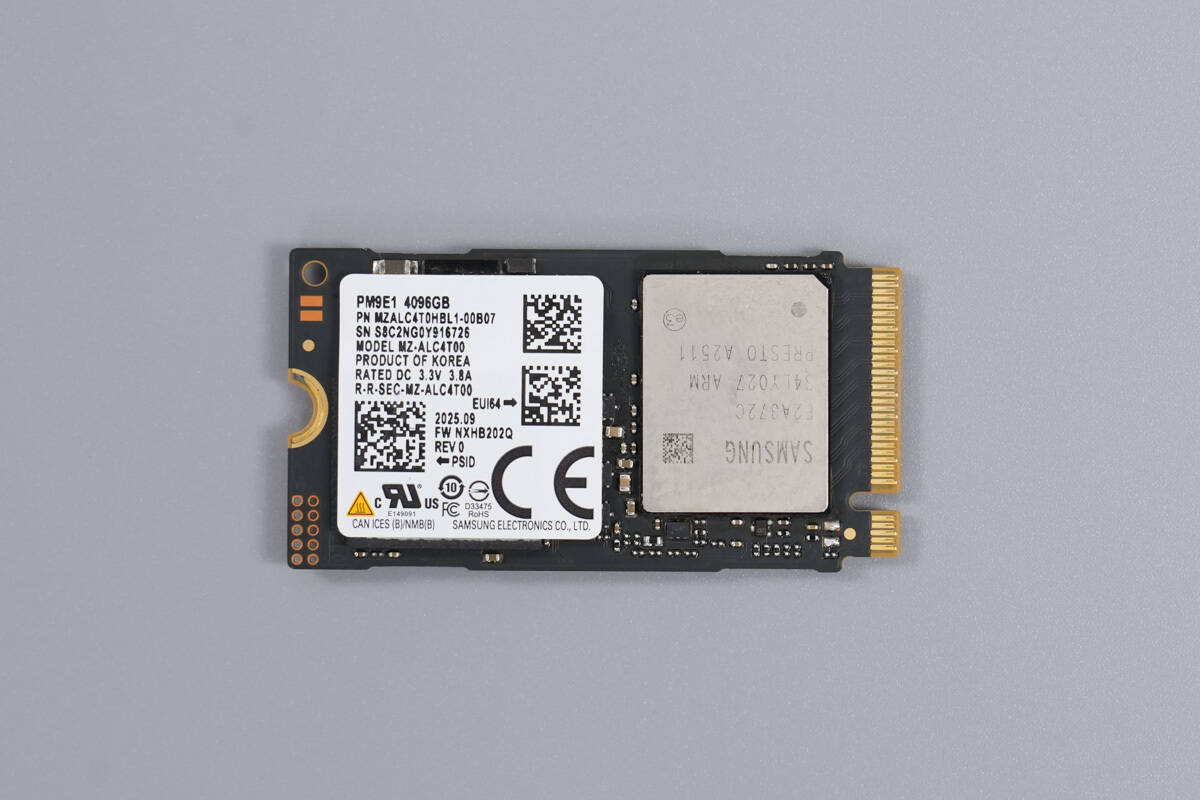
The SSD is from Samsung, model PM9E1, with a capacity of 4096 GB and a 2242 form factor.
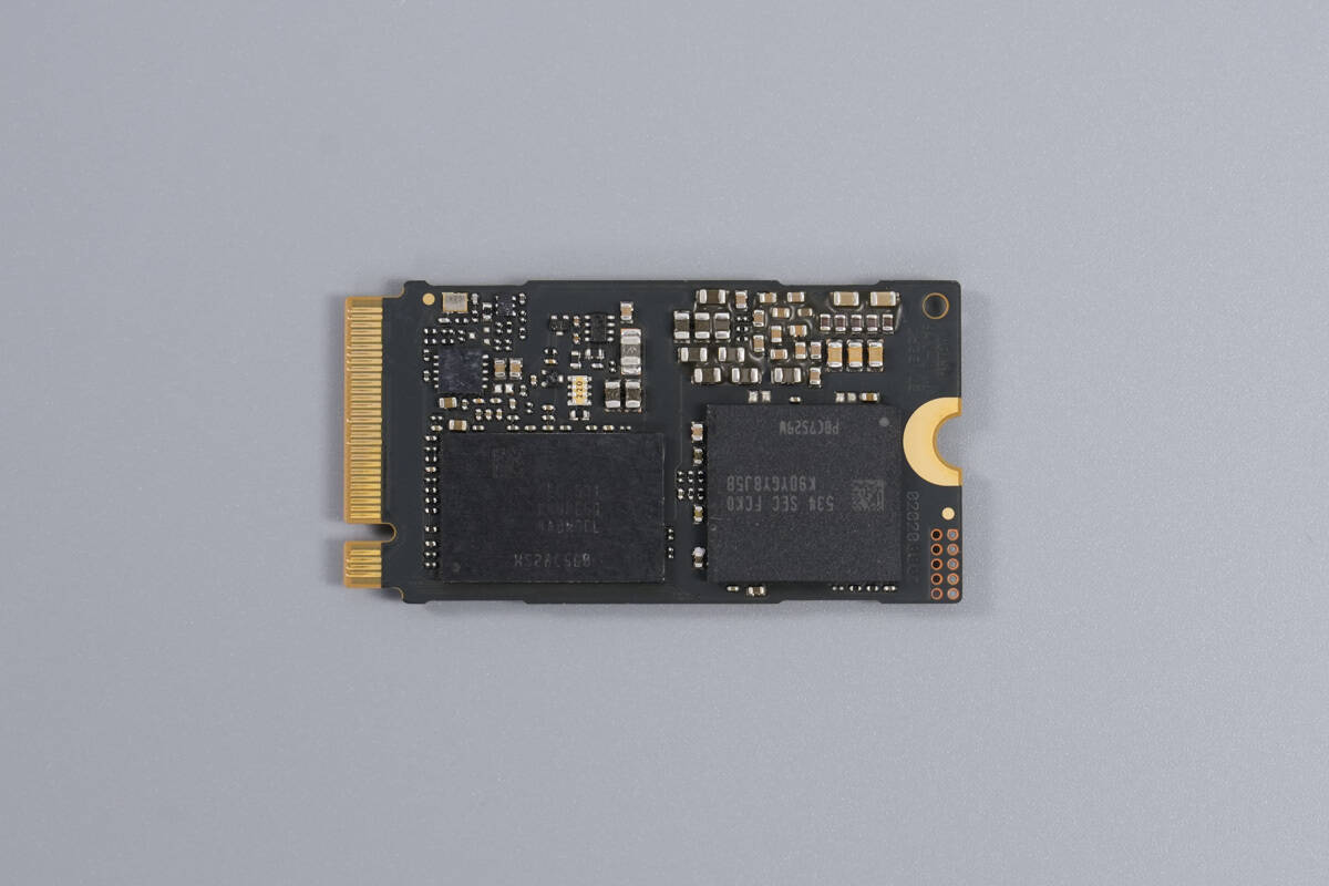
The SSD has a double-sided design, with the controller and flash memory chips on the front, and memory chips and flash memory chips on the back.
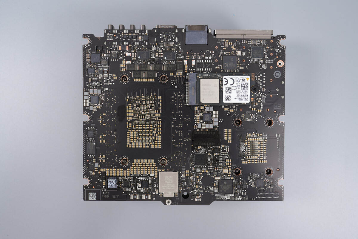
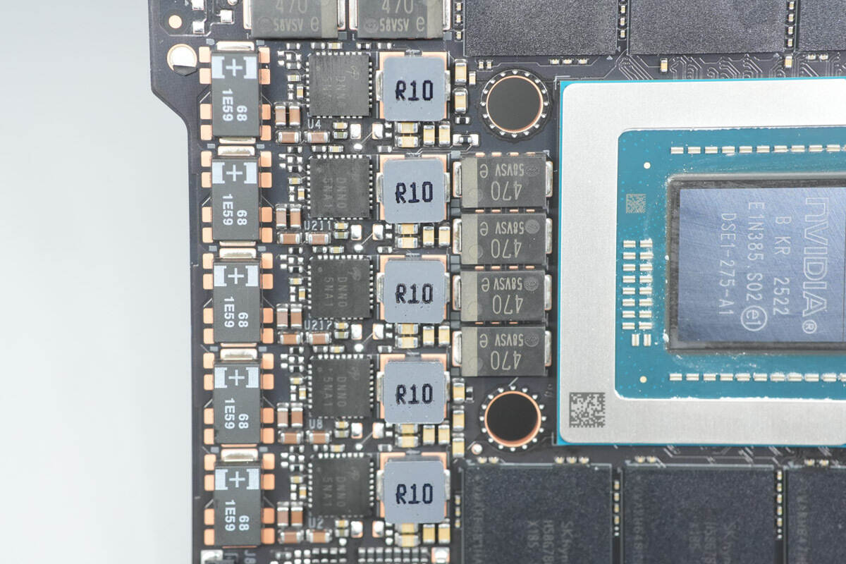
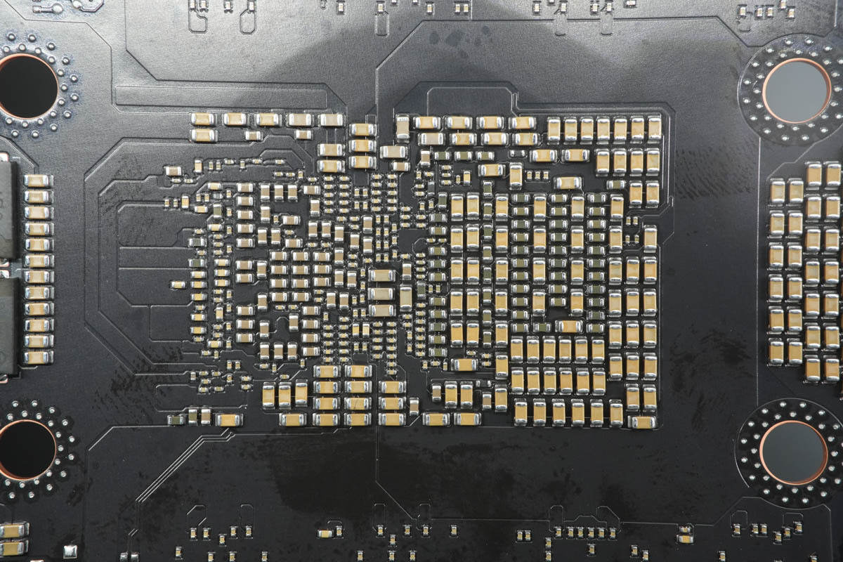
Overview of the front side of the PCBA module.
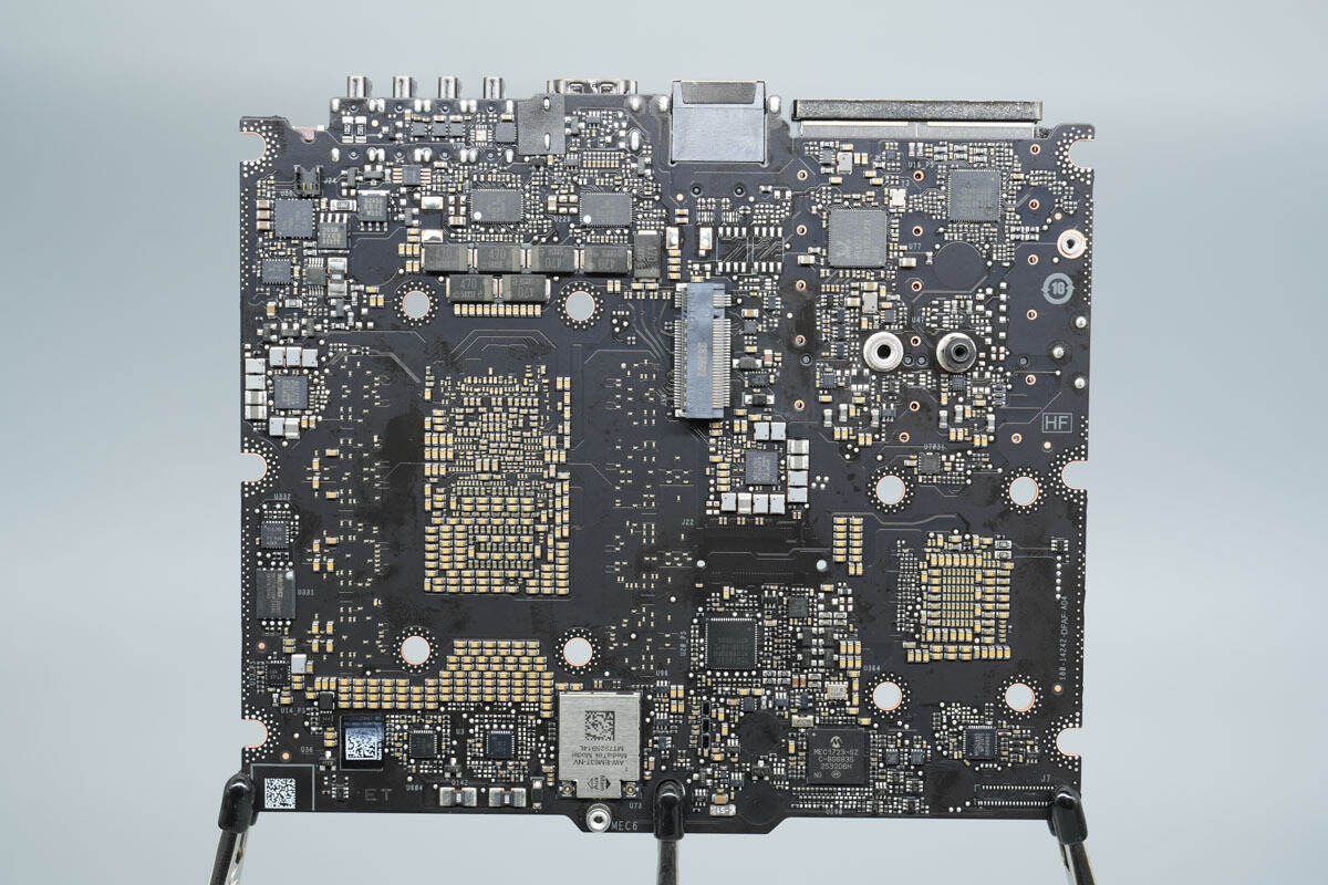
Overview of the back side of the PCBA module.
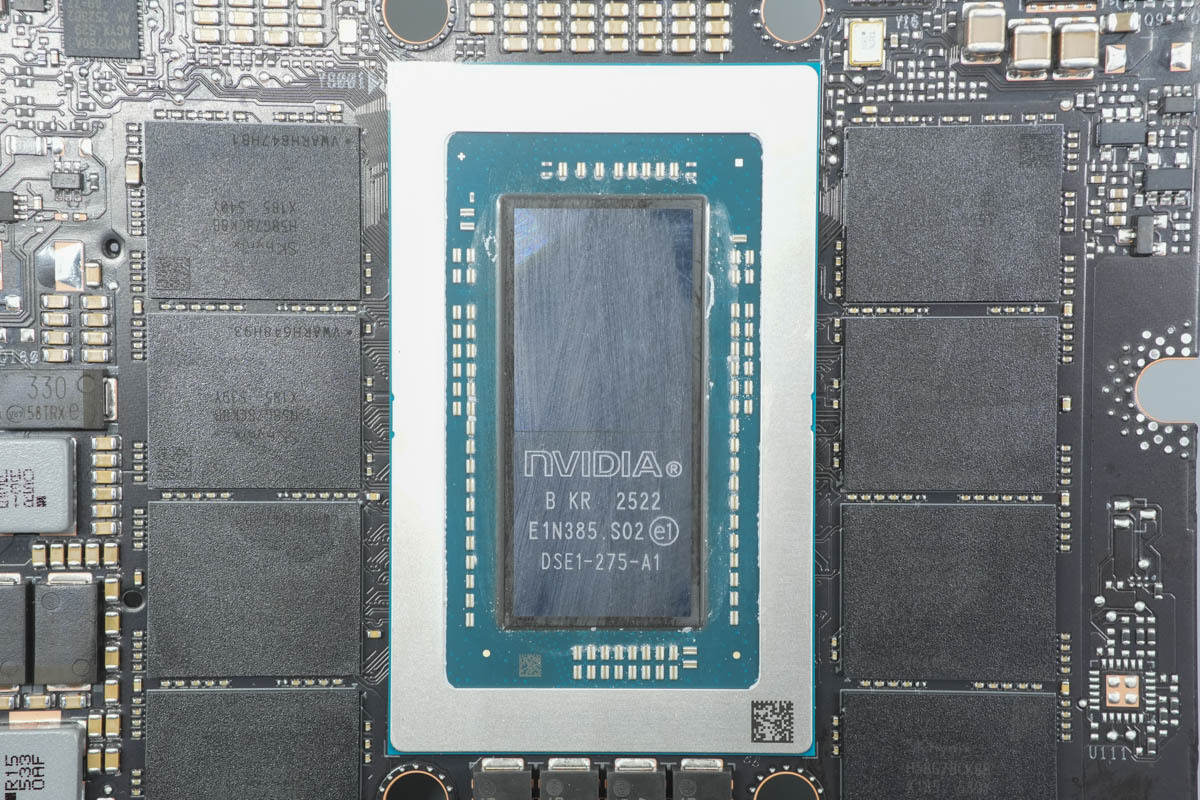
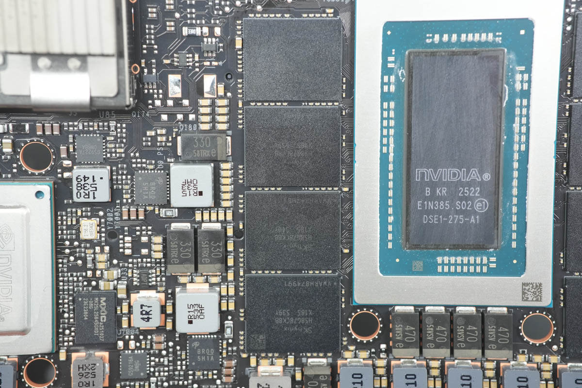
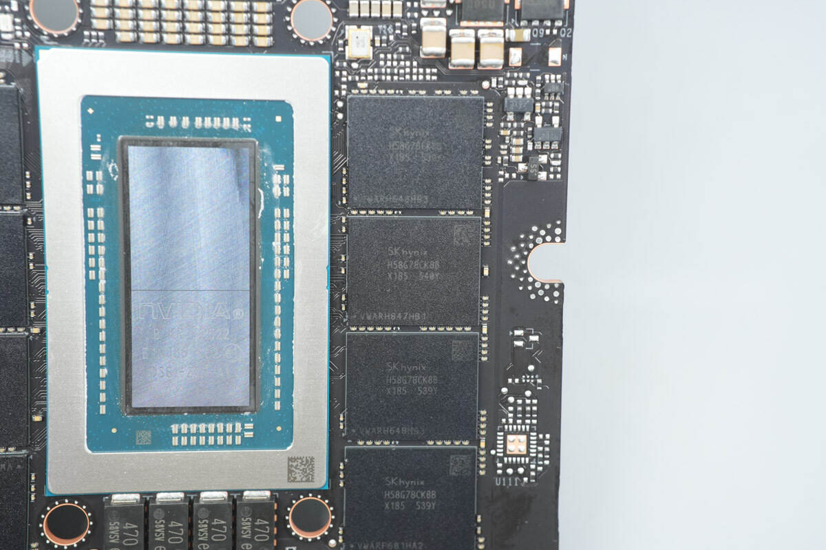
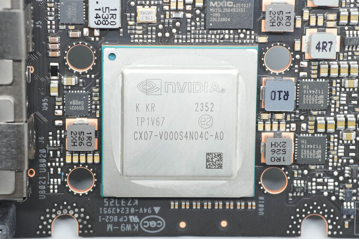
The NVIDIA GB10 superchip has a reinforced metal frame along the edges. The chip is marked with B KR 2522 E1N385.S02 DSE1-275-A1. It is manufactured using TSMC’s N3 3nm process and features a 2.5D package. The rectangular area on top is the SoC region, while the nearly square area below is the GPU region.
There are four memory chips located on the left side.
There are also four memory chips on the right side.
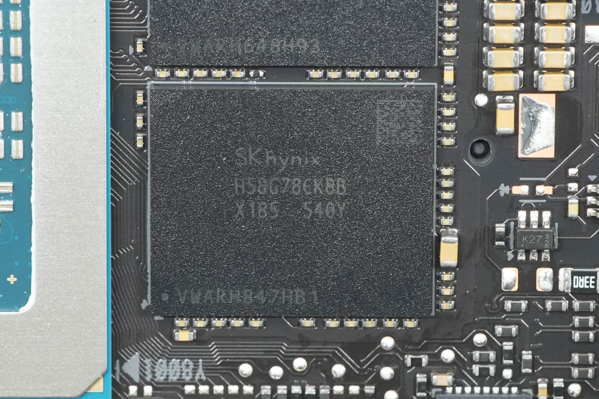
The memory chips are from SK Hynix, model H58G78CK8BX185. They are LPDDR5X memory, each with a capacity of 16 GB, using a 315-ball FBGA package.
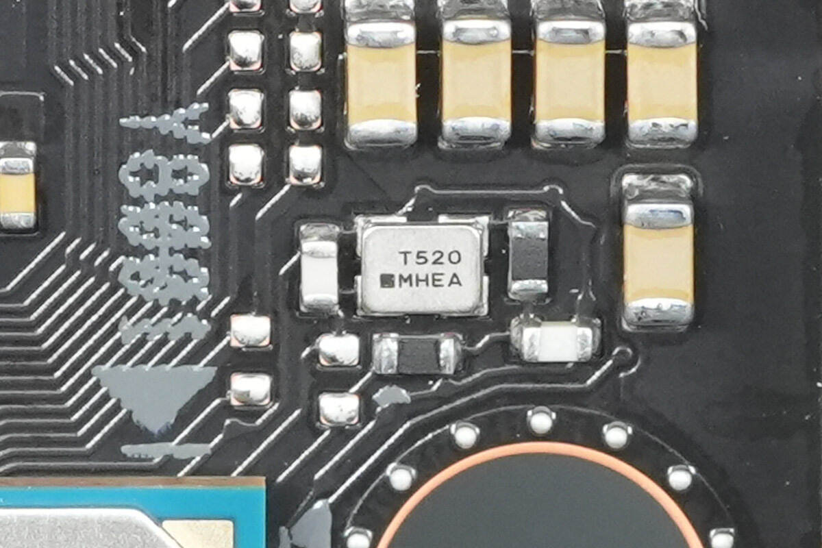
Close-up of the clock crystal oscillator.
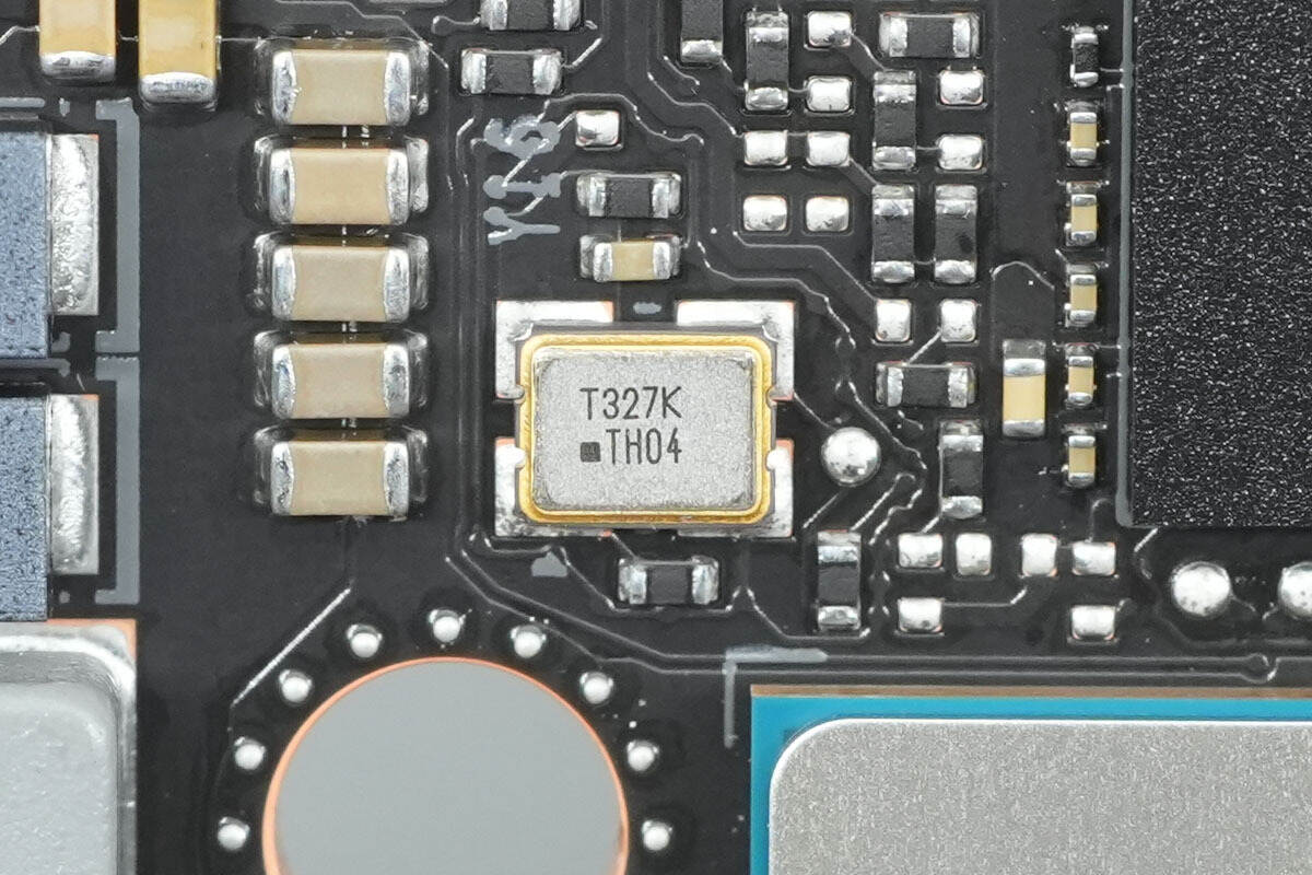
Close-up of another clock crystal oscillator.
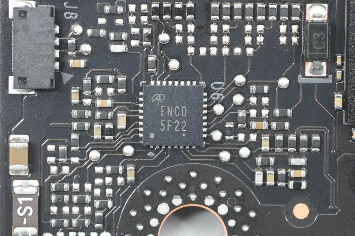
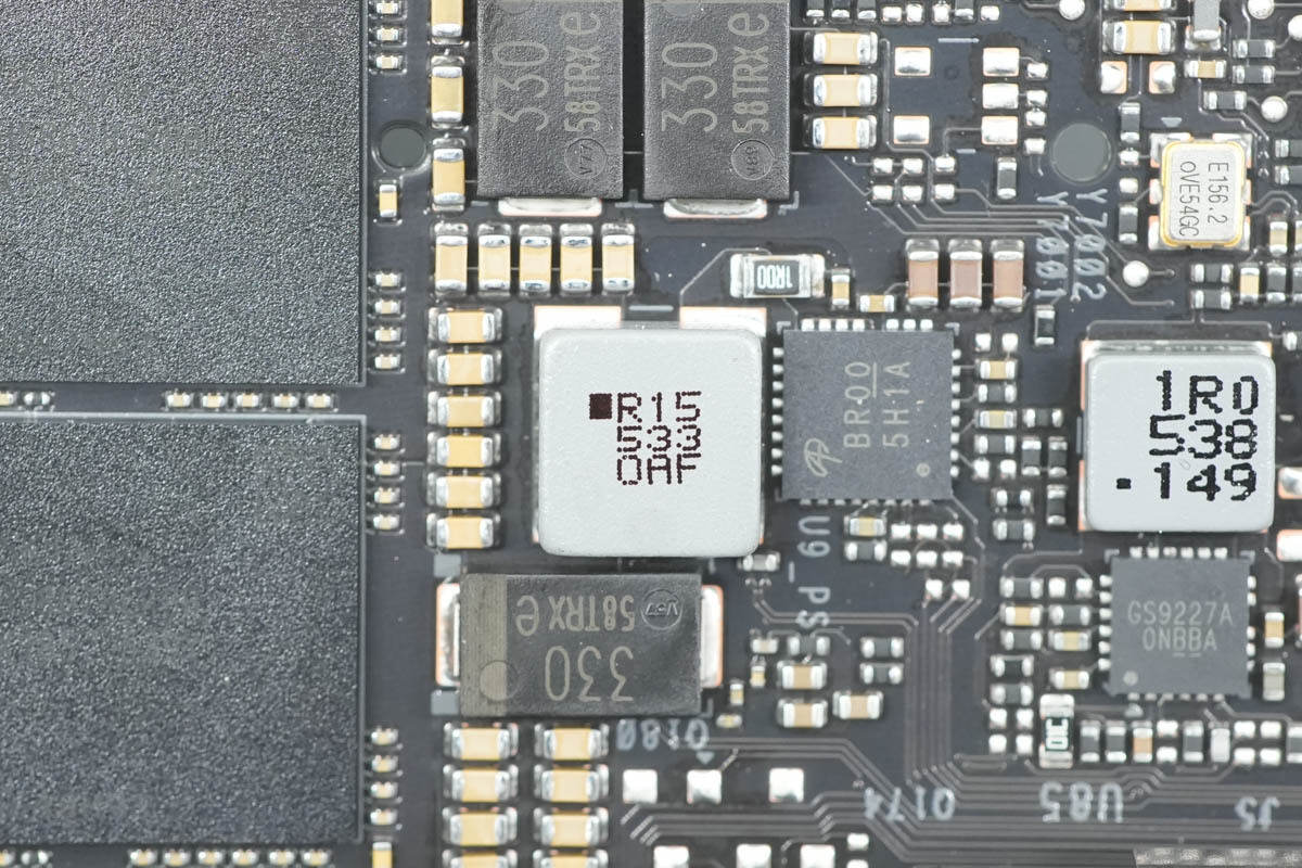
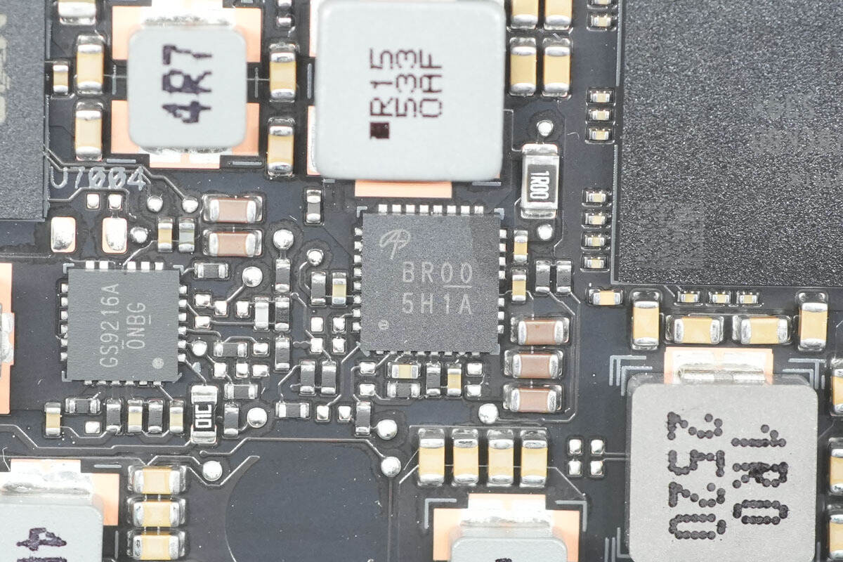
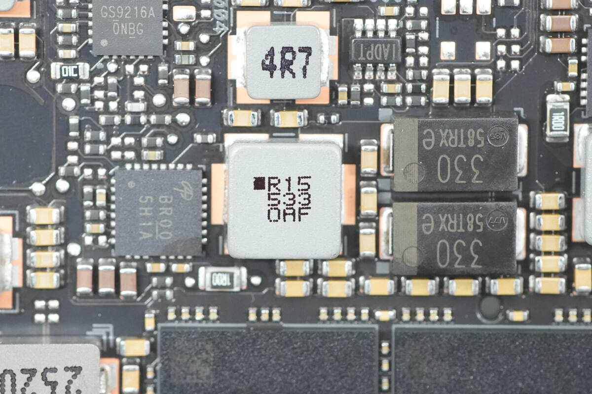
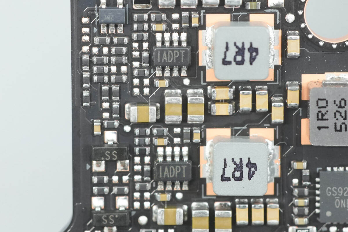
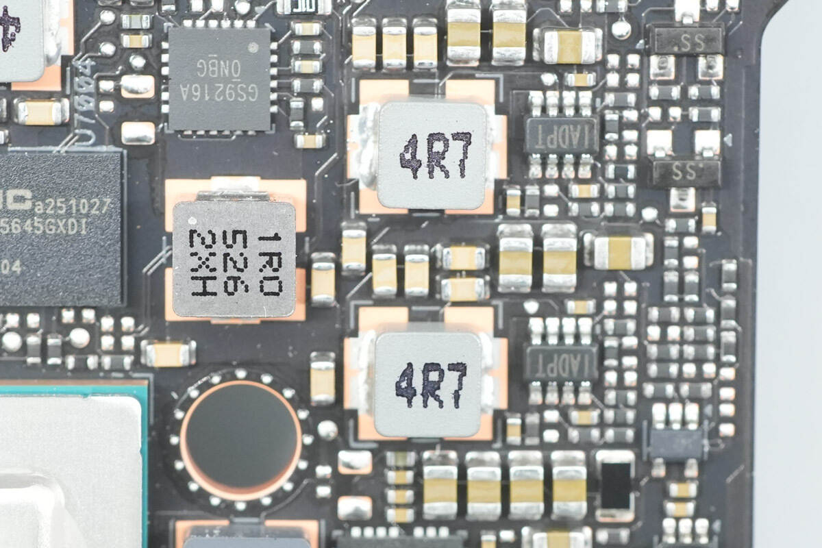
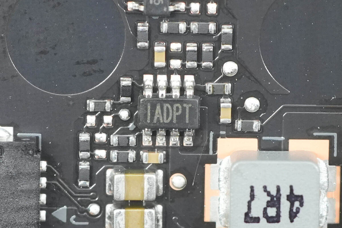
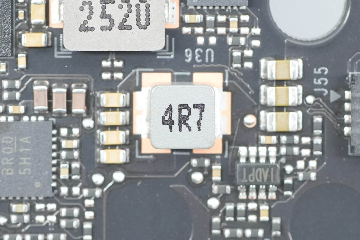
The multi-phase power controller is from AOS, marked ENC0, model AOZ73004CQI. This chip is designed for the Blackwell GPU platform and complies with the OVR-4-22 standard. It supports 4-phase applications and features a proprietary high-performance advanced transient regulator control scheme, dynamic phase current balancing, and seamless CCM-to-DCM control. The chip comes in a 4×4 mm QFN-32L package.
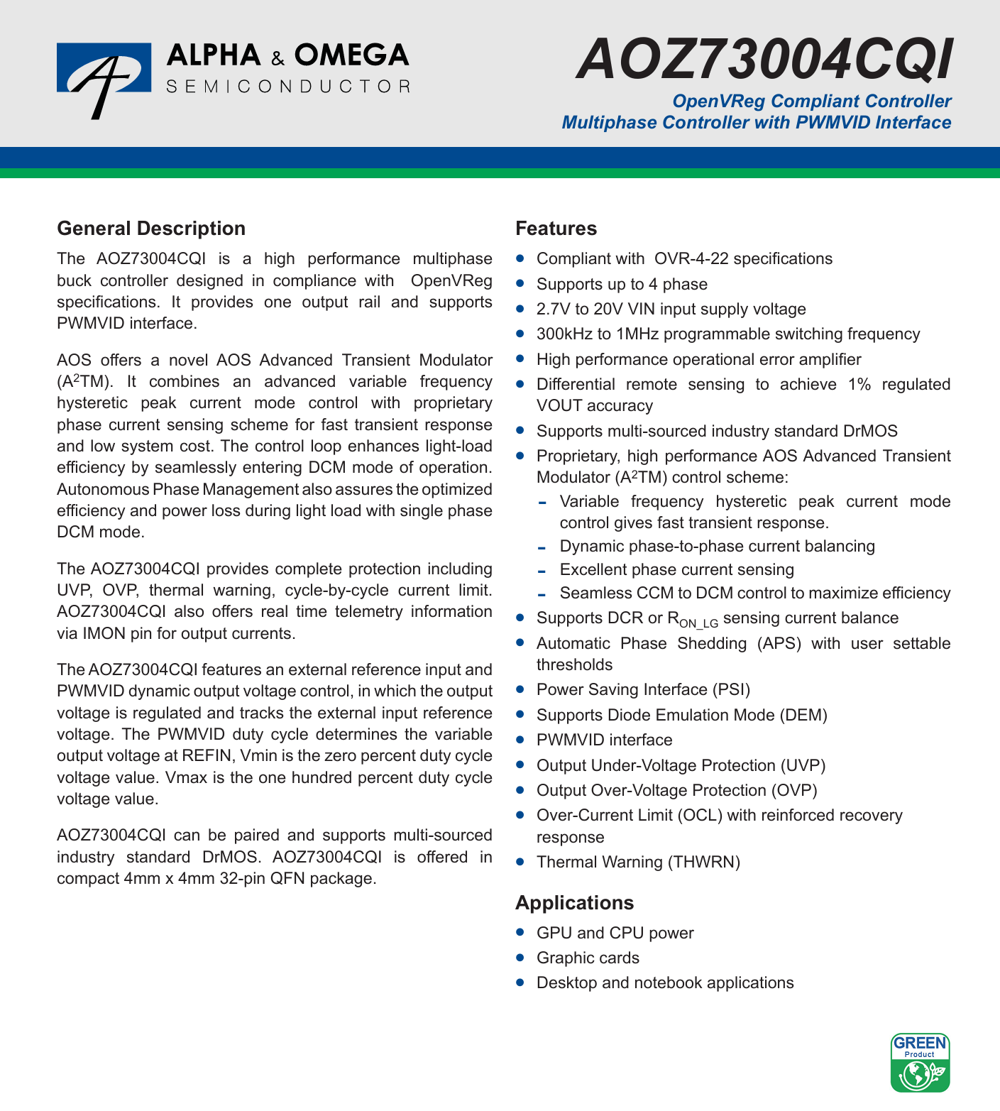
Here is the information about AOS AOZ73004CQI.
The other multi-phase buck controller also uses the AOS AOZ73004CQI.
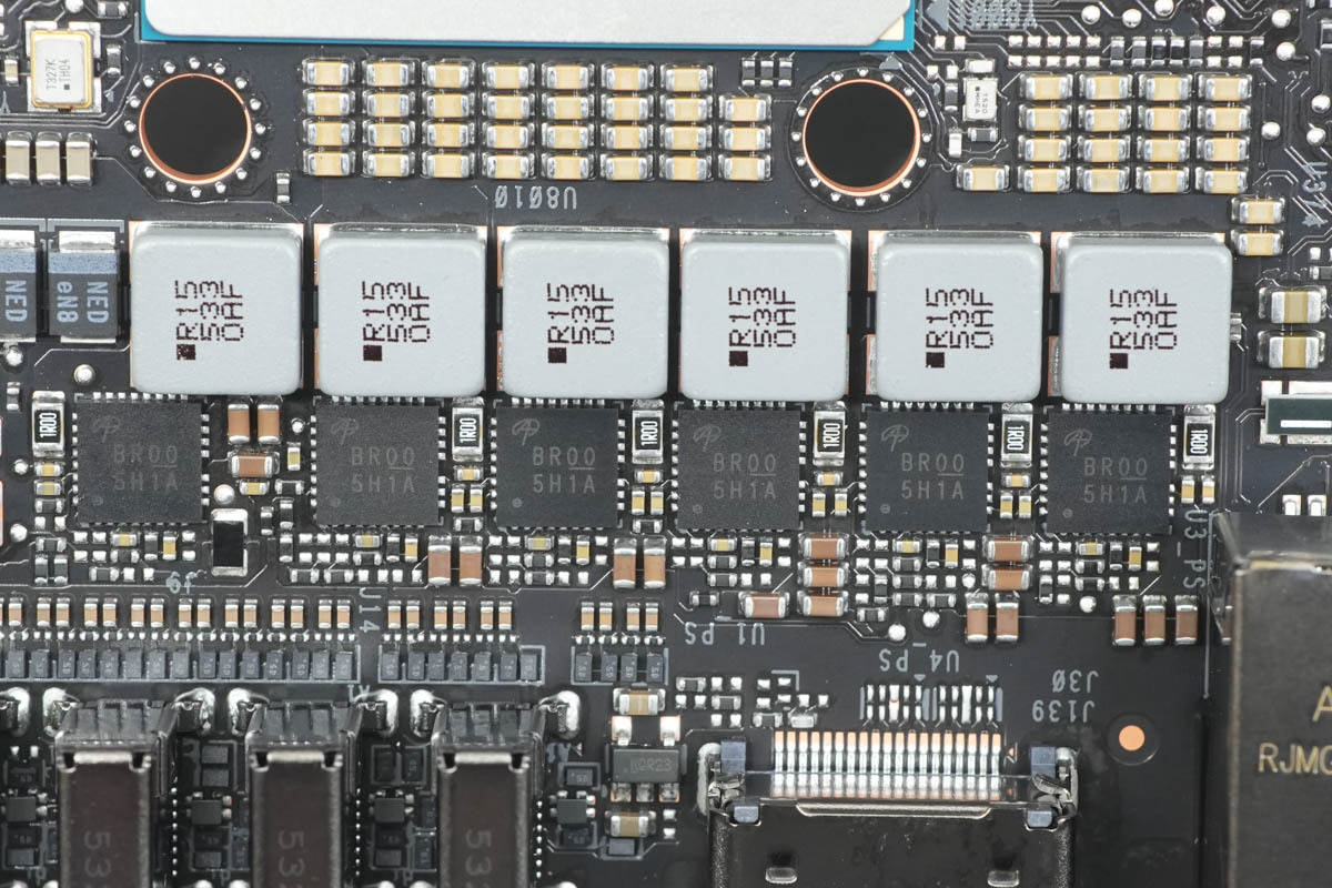
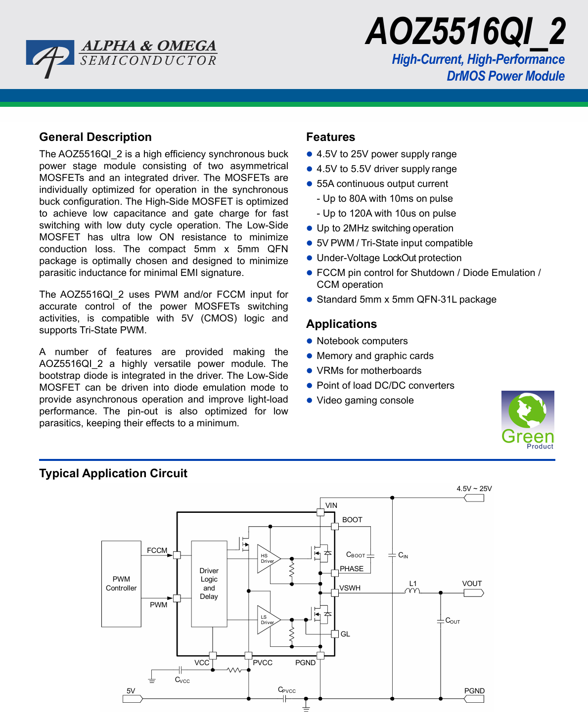
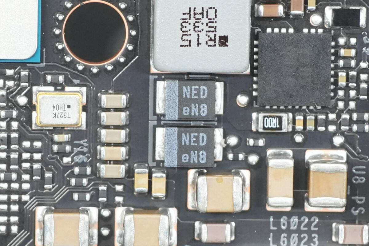
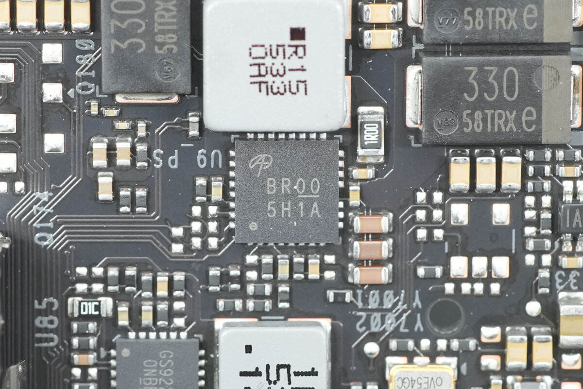
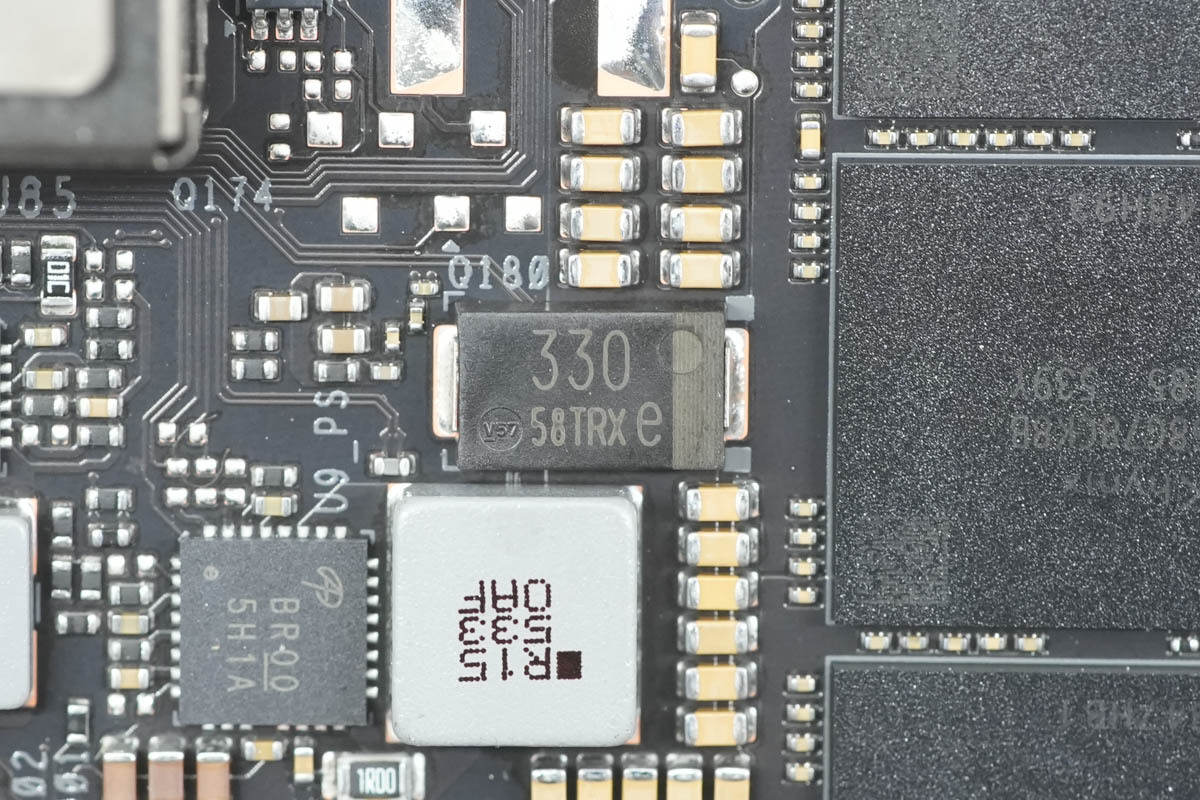
The DrMOS components are from AOS, marked BR00, model AOZ5516QI_2. They are high-performance, high-current DrMOS devices, supporting an input voltage range of 4.5–25V, with a continuous output current capability of 55A. The switching frequency can reach up to 2 MHz. They support 5V PWM and tri-state inputs, feature under-voltage lockout protection, and are packaged in a 5×5 mm QFN-31L package.
Here is the information about AOS AOZ5516QI_2.
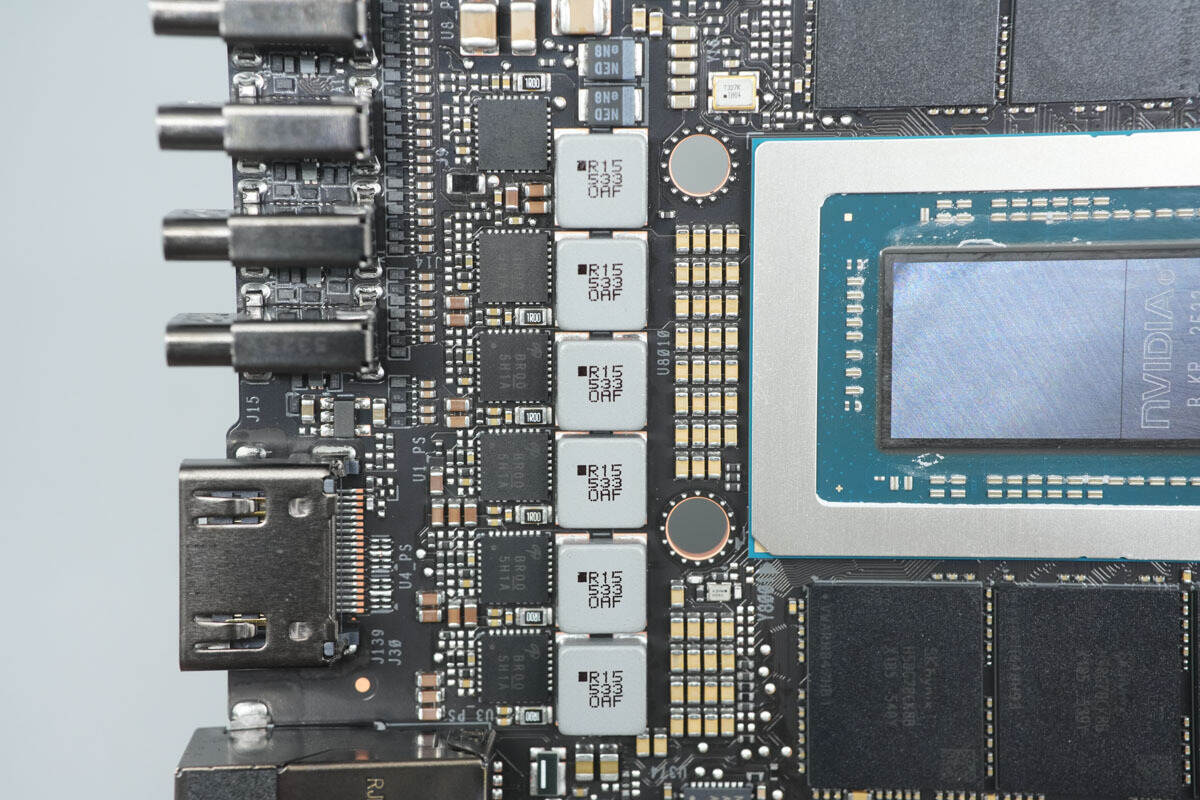
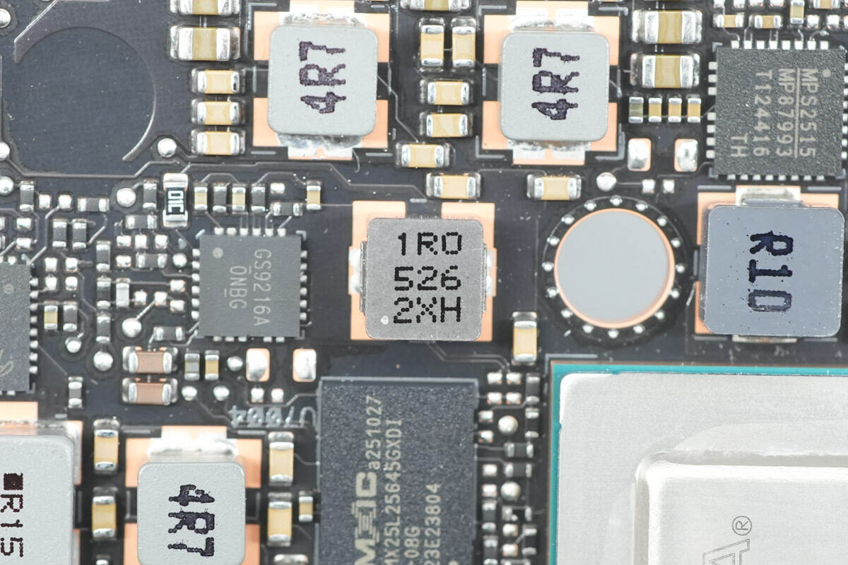
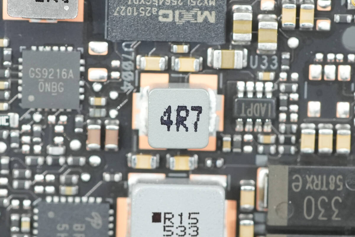
Close-up of the 0.15μH buck inductors.
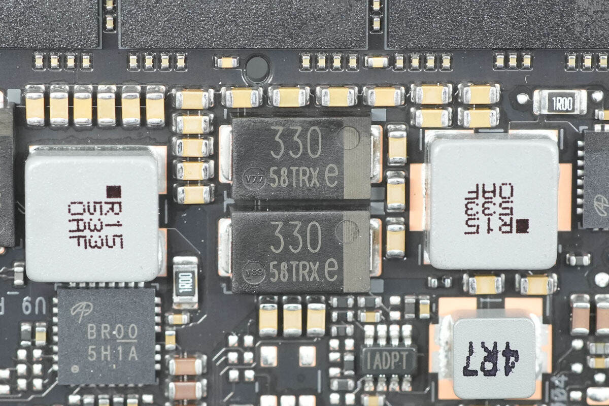
The polymer tantalum capacitor is from KEMET, with a specification of 2.5V and 330 μF.
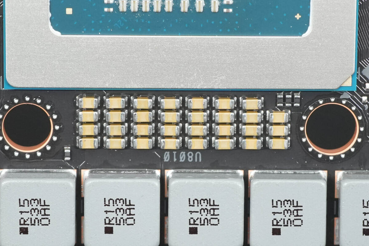
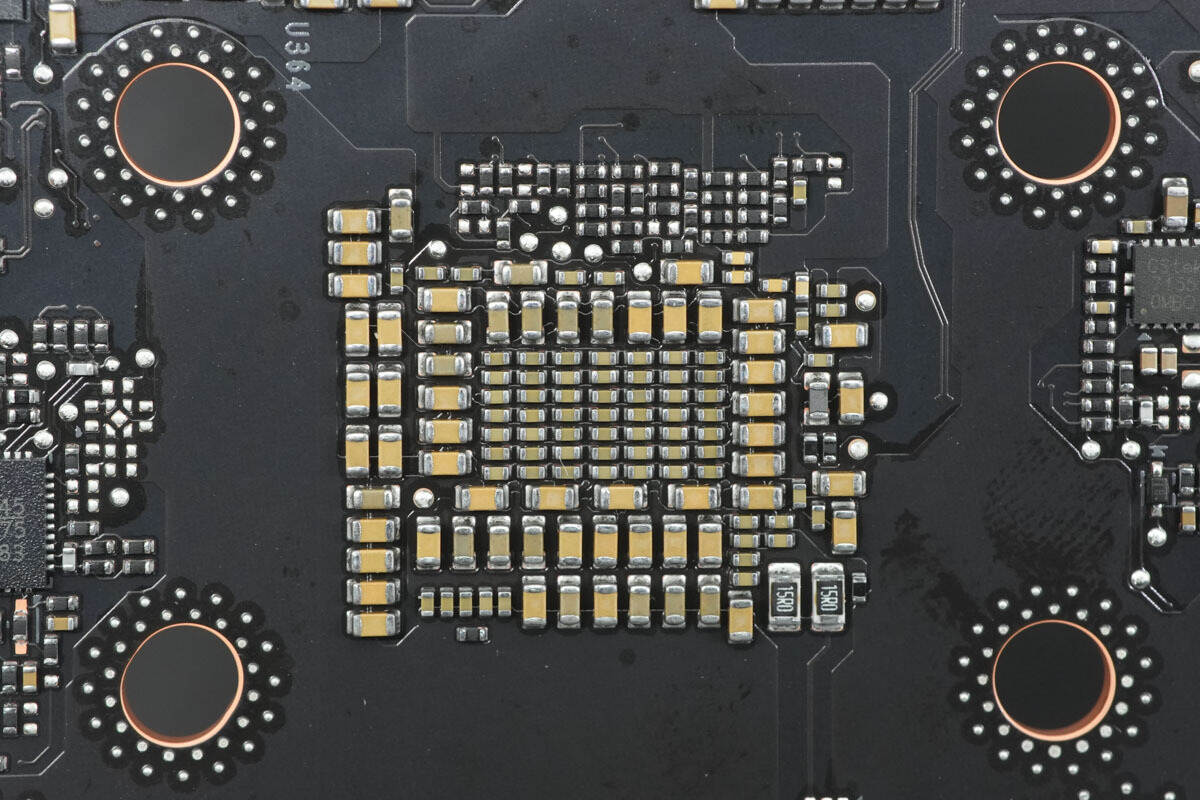
A close-up of the MLCC capacitors used for filtering.
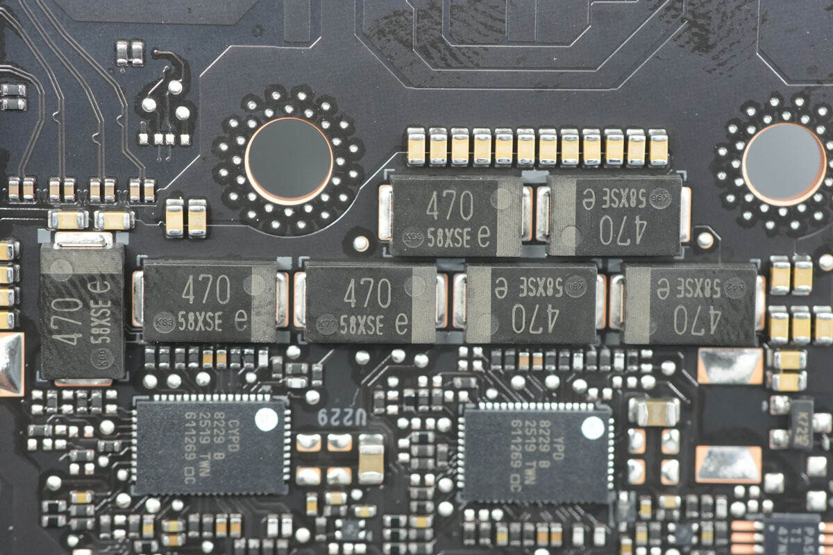
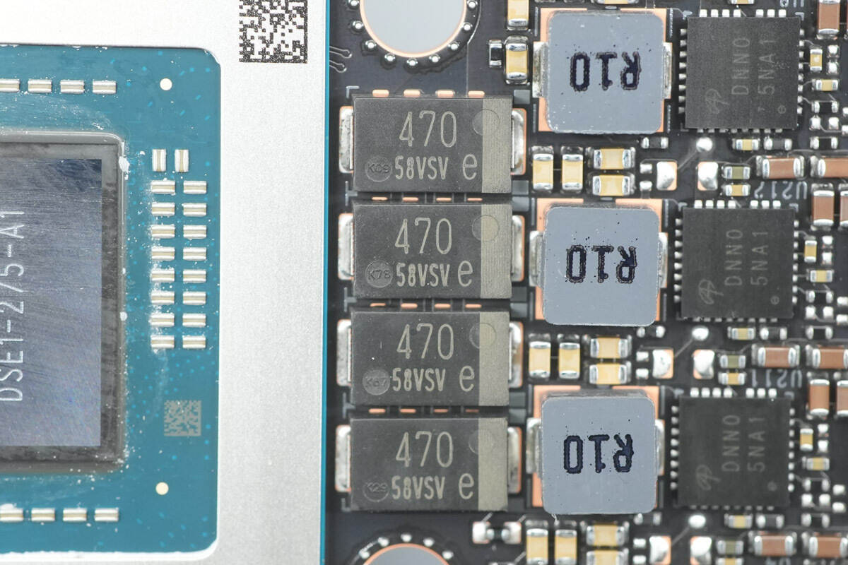
The backside of the PCBA module is equipped with seven filtering capacitors, rated at 470 μF, 2.5V.
The DrMOS uses the AOS AOZ5516QI.
A close-up of the 0.15 μH buck inductor.
The filtering capacitors are from Panasonic, part of the SPCAP series, rated at 330 μF, 2.5V.
DrMOS uses AOS AOZ5516QI_2.
Close-up of the 0.15μH buck inductor.
The filter capacitor is rated at 330μF 2.5V.
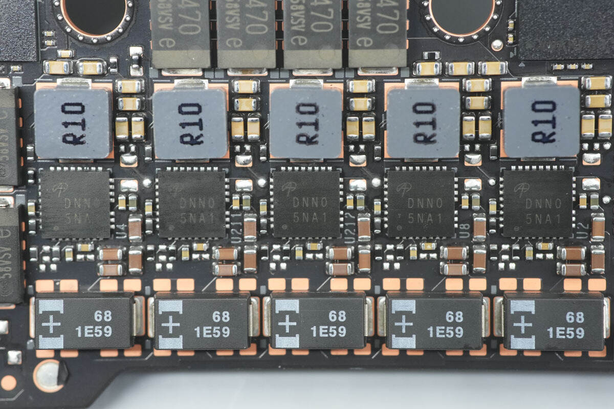
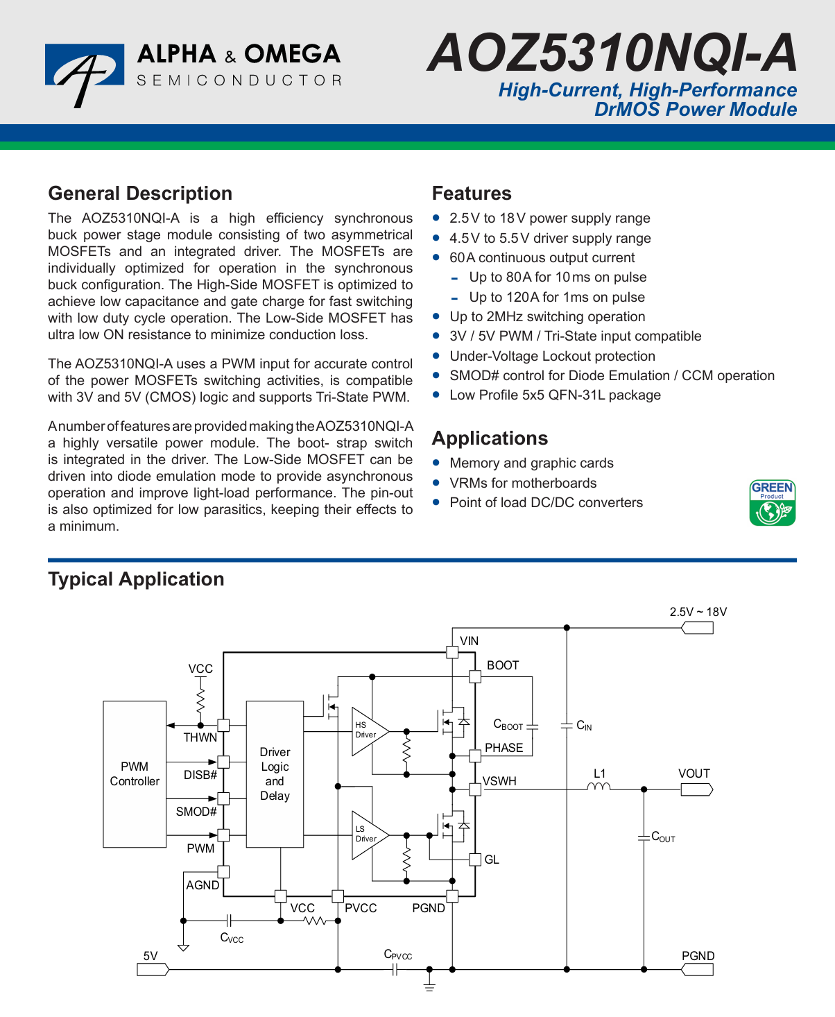
The lower DrMOS devices are also from AOS, marked with DNN0 and identified as AOZ5310NQI-A. They are high-performance, high-current DrMOS devices supporting a 4.5–18V supply range, with up to 60A continuous output current. The switching frequency reaches 2 MHz, and they support 3V/5V PWM and tri-state inputs. They also feature undervoltage lockout protection and come in a QFN 5×5-31L package.
Here is the information about AOS AOZ5310NQI-A.
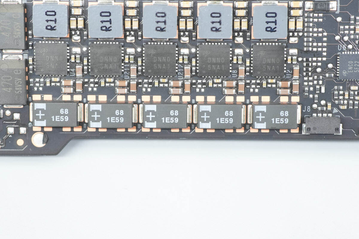
The filter capacitors are from Panasonic and are rated at 68μF 25V.
Close-up of the 0.1μH buck inductors.
The filter capacitors are rated at 470μF 2.5V.
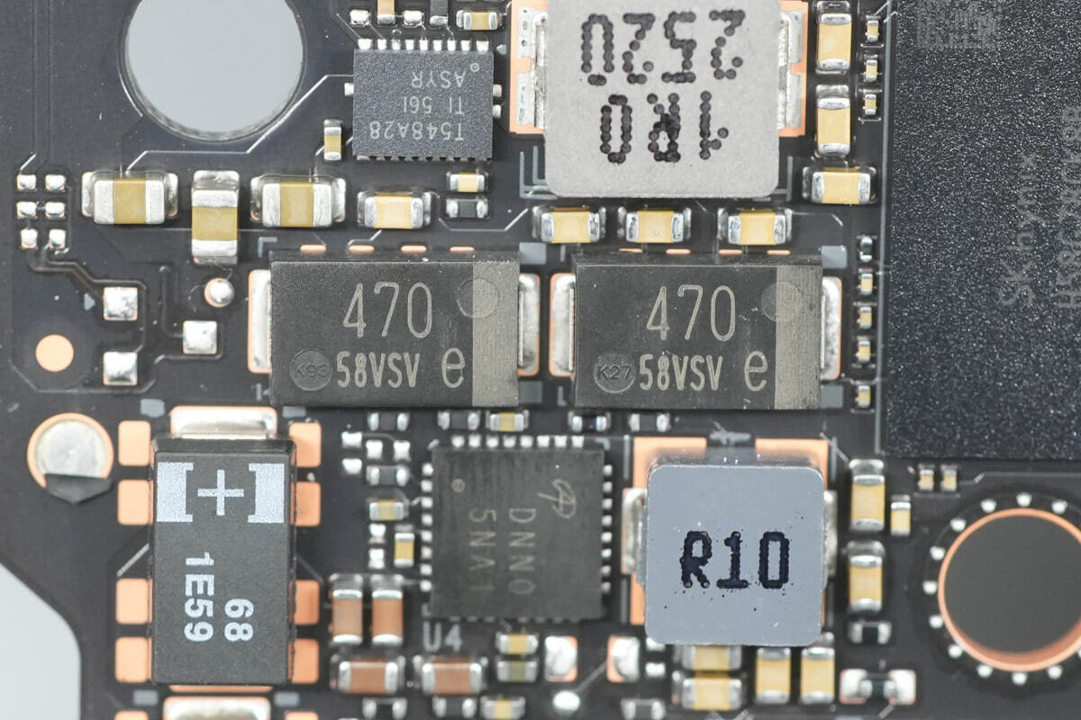
These two filter capacitors have the same specifications.
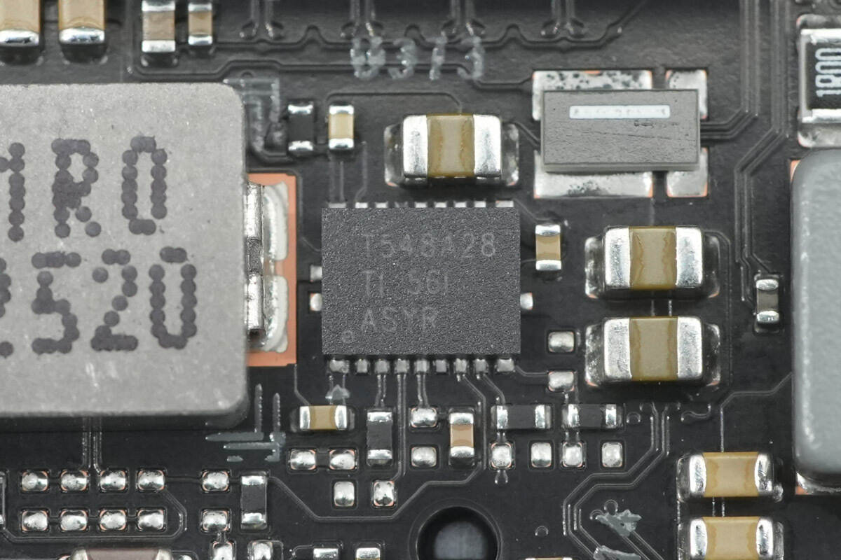
The synchronous buck converter is from Texas Instruments, model TPS548A28. It is a synchronous buck converter with remote sensing and an integrated 3V LDO, supporting an input voltage range of 2.7–16V and delivering up to 15A output current. It comes in a VQFN-HR21 package.
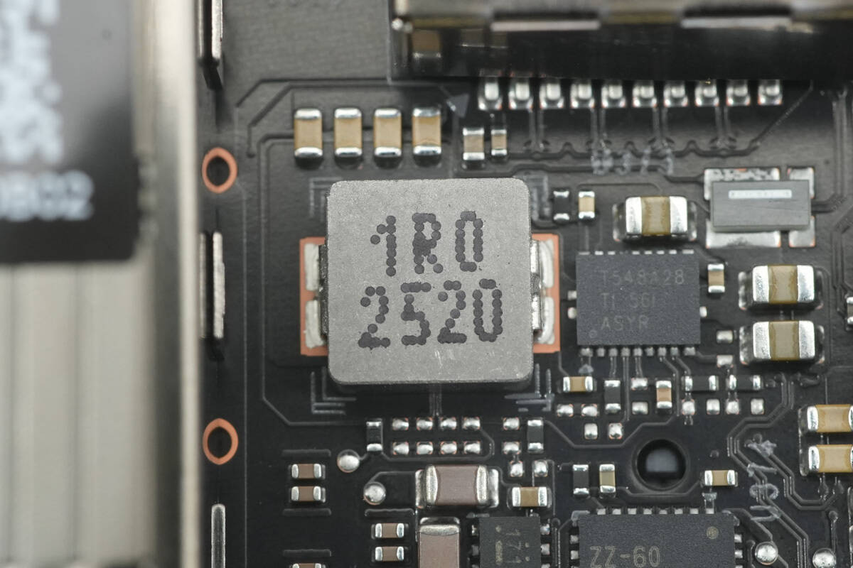
Close-up of the 1μH buck inductor.
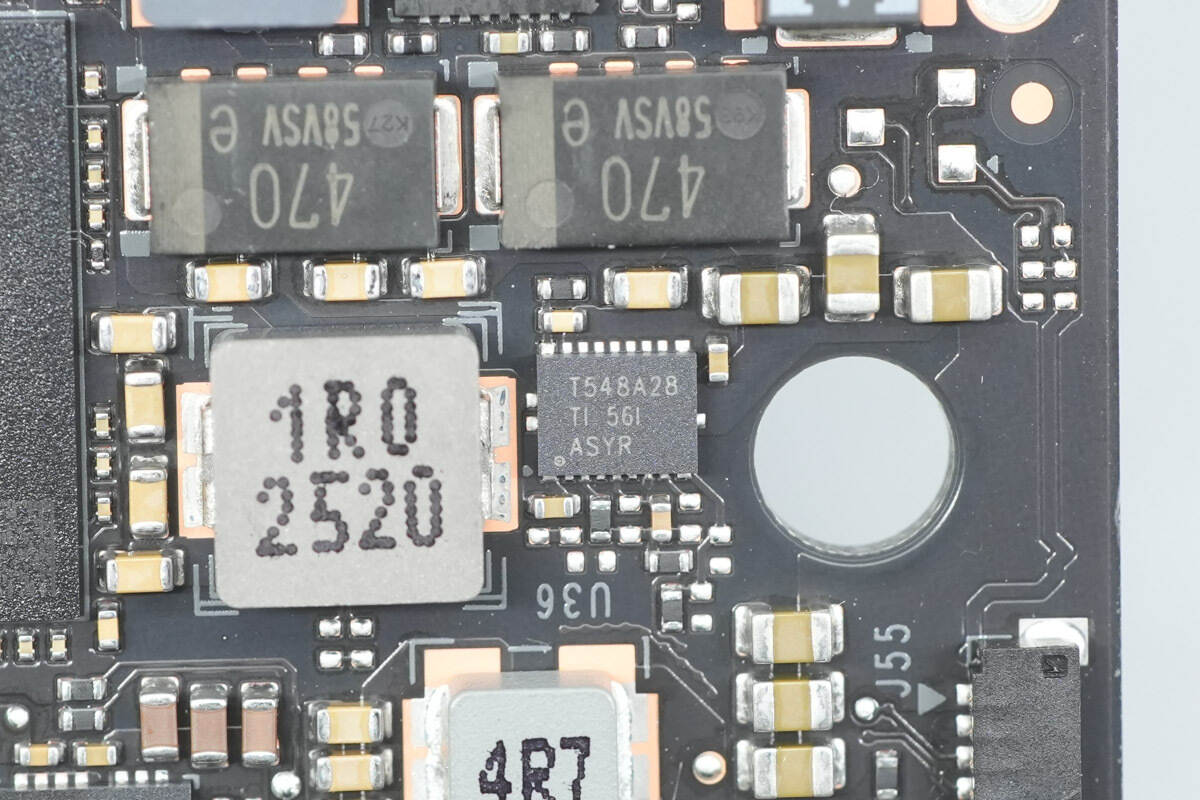
The other synchronous buck chip is of the same model.
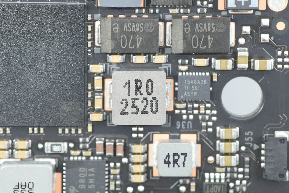
A close-up of the 1μH buck inductor used in conjunction with the device.
Close-up of the MLCC filter capacitors on the back.
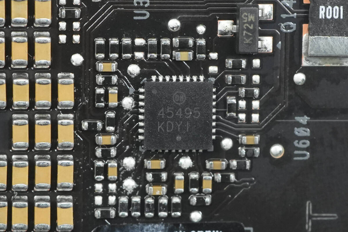
The voltage monitoring chip is from Onsemi, model NCP45495. It is a chip that supports 26V input voltage, has 4 channels for voltage and current monitoring, and is packaged in QFN32.
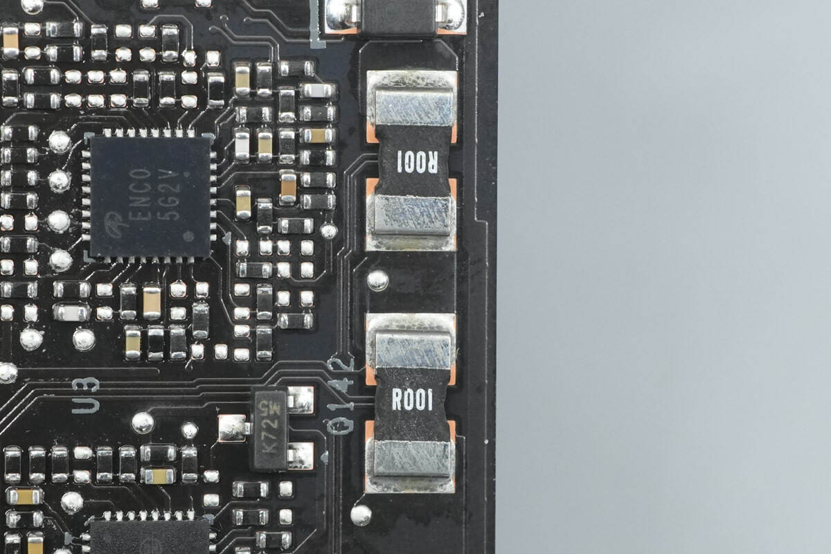
Two 1mΩ resistors are used for current detection.
Close-up of the input MLCC filter capacitors.
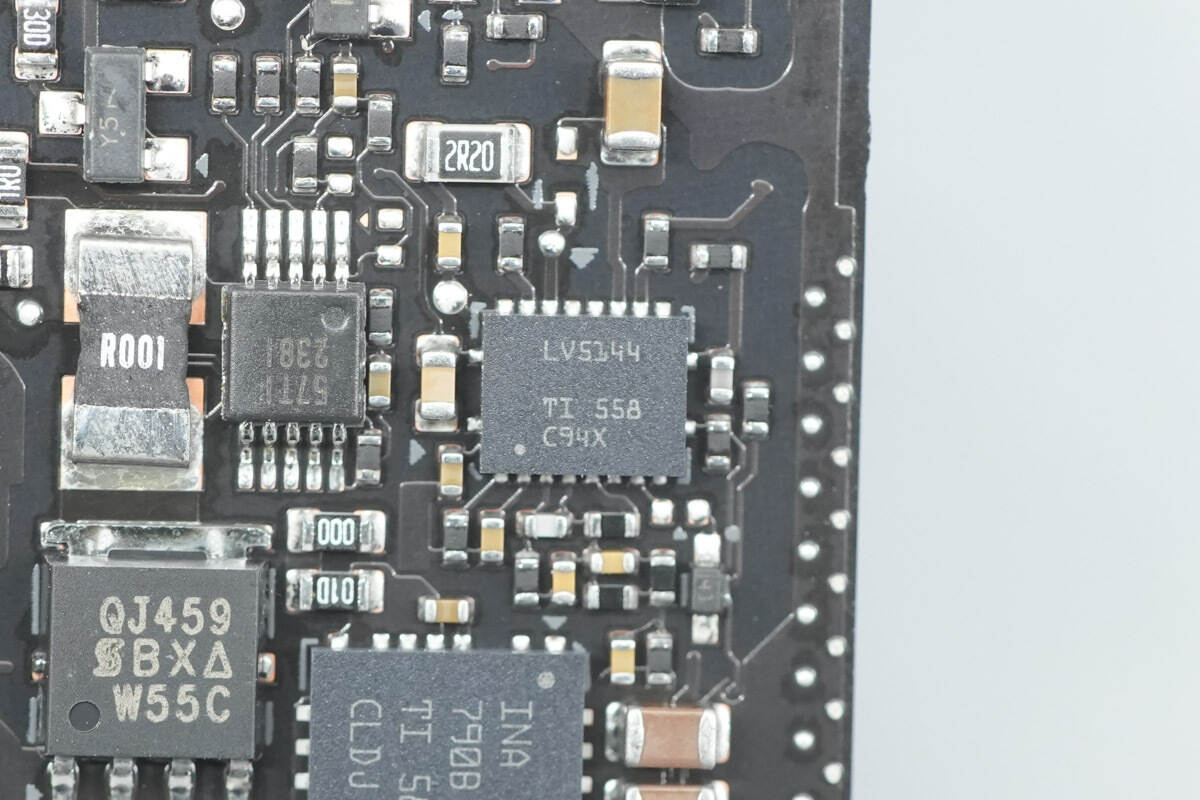
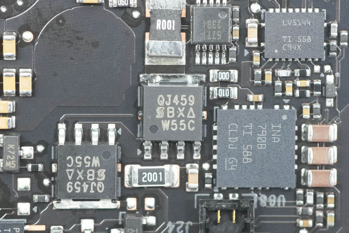
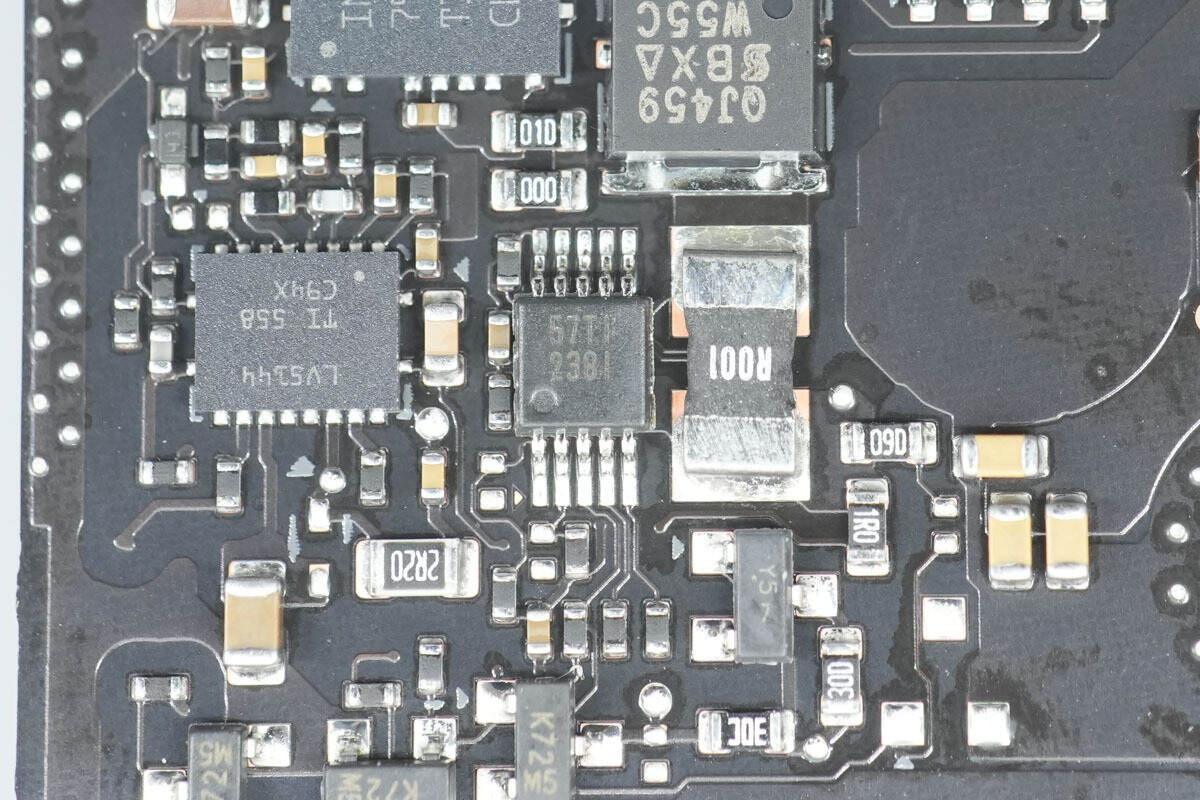
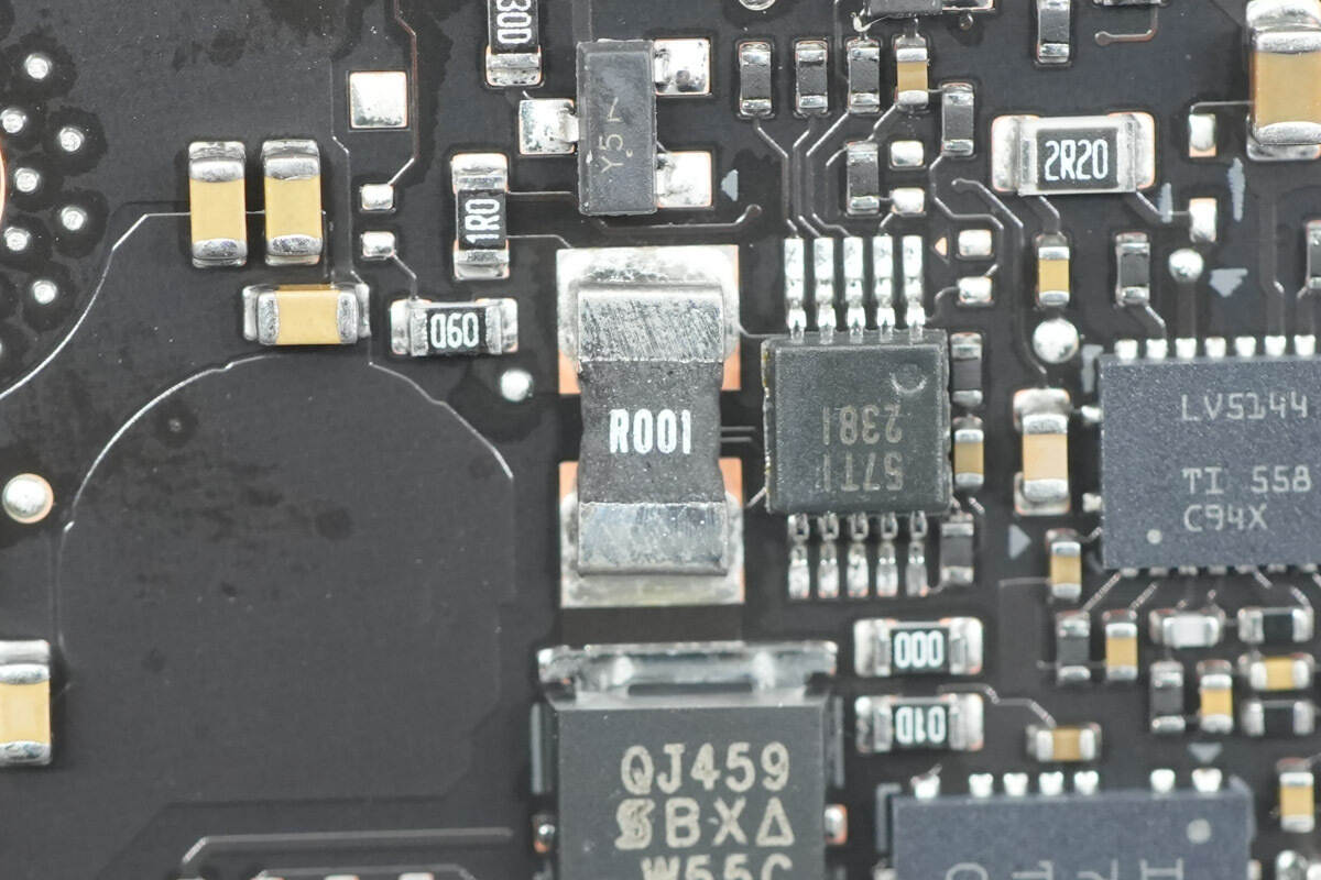
The synchronous buck controller is from Texas Instruments, model LV5144. It features a wide duty cycle range, supports a 6–95V operating voltage range, and provides an output voltage range of 0.8–60V. The switching frequency is adjustable from 100 kHz to 1 MHz, and it comes in a VQFN-20 package.
The synchronous buck MOSFETs are from Vishay.
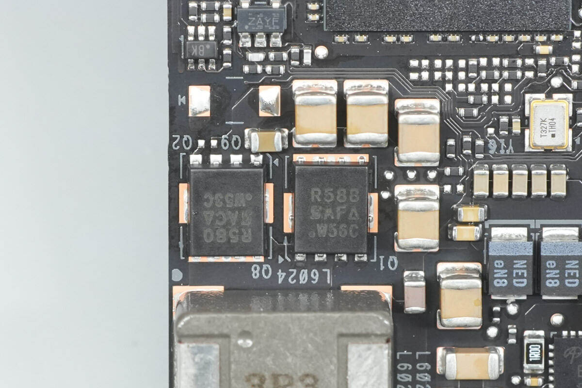
The high-side MOSFET is marked with R588, identified as SiR588DP. It is rated for 80V with an on-resistance of 8 mΩ, and comes in a PowerPAK SO-8 package.
The low-side MOSFET is marked with R580, identified as SiR580DP. It is also rated for 80V, with a lower on-resistance of 2.7 mΩ, and is housed in a PowerPAK SO-8 package.
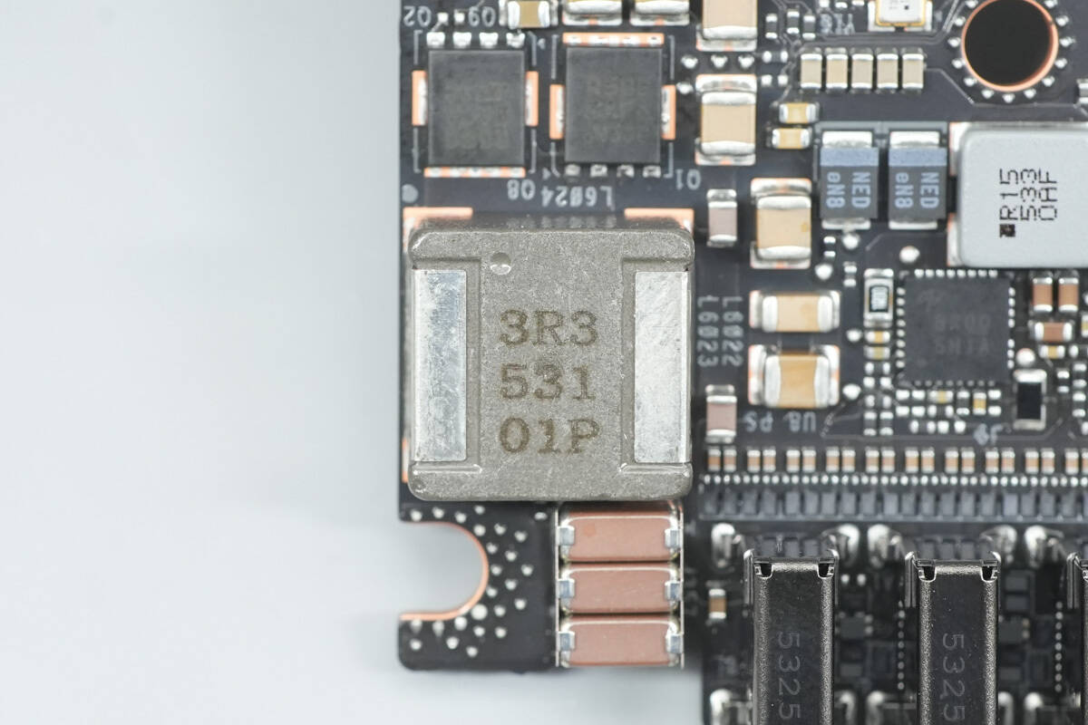
Close-up of a 3.3μH buck inductor.
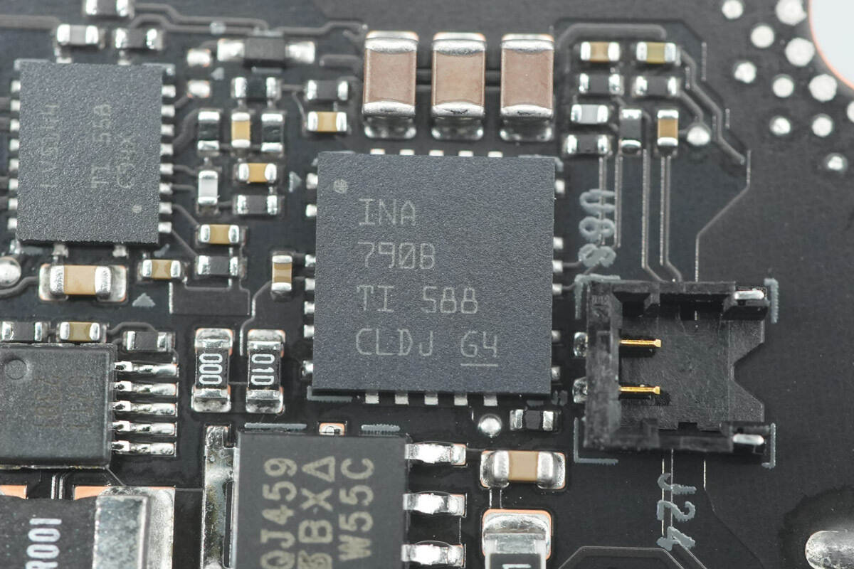
The current sense amplifier is from Texas Instruments, model INA790B. It supports a voltage range of -4V to 110V, integrates a 0.4 mΩ current-sense resistor, and supports up to 75A continuous current. It comes in a VQFN-15 package.
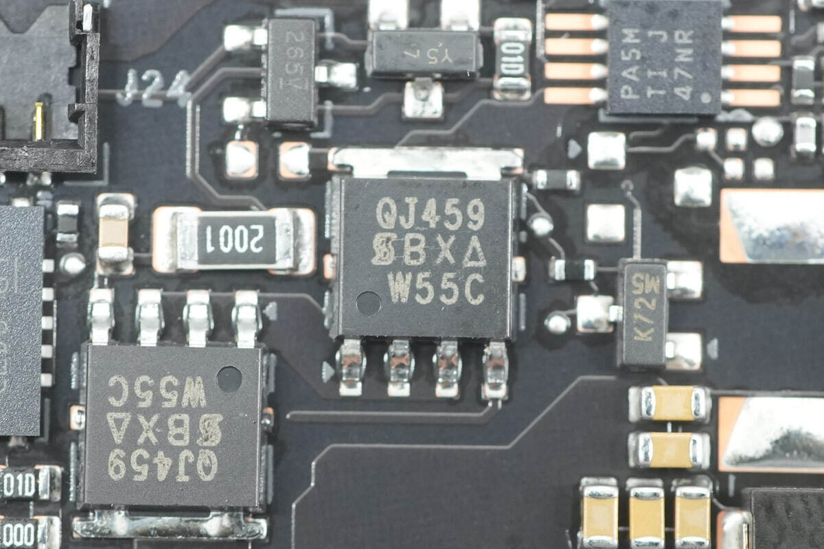
The VBUS MOSFET is from Vishay, model SQJ459EP. It is a PMOS device rated for 60V, with an on-resistance of 18 mΩ, and comes in a PowerPAK SO-8L package.
The other VBUS MOSFET is of the same model.
The power monitoring chip is from Texas Instruments, marked with 238I and identified as INA238. It is a 16-bit high-precision power monitor with an 85V rating and an I²C interface, and comes in a VSSOP-10 package.
Close-up of a 1mΩ current sensing resistor.
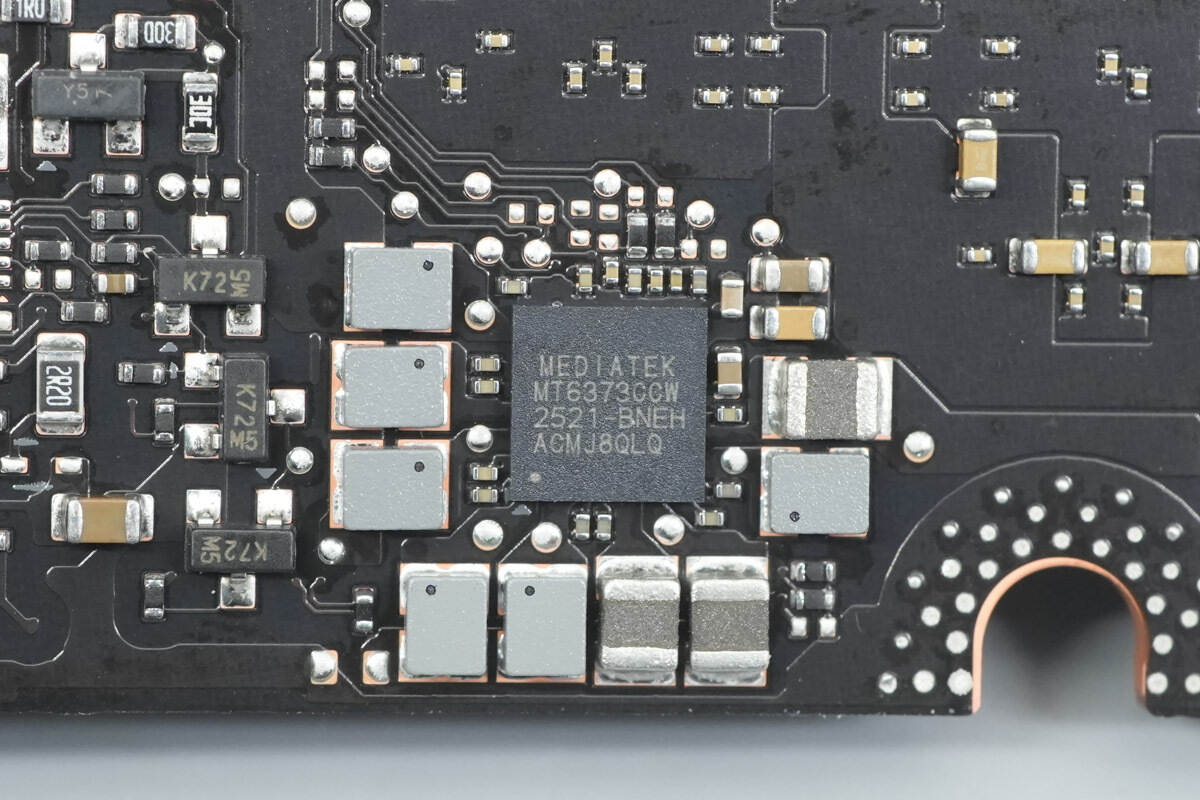
The PMIC is from MediaTek, model MT6373CCW.
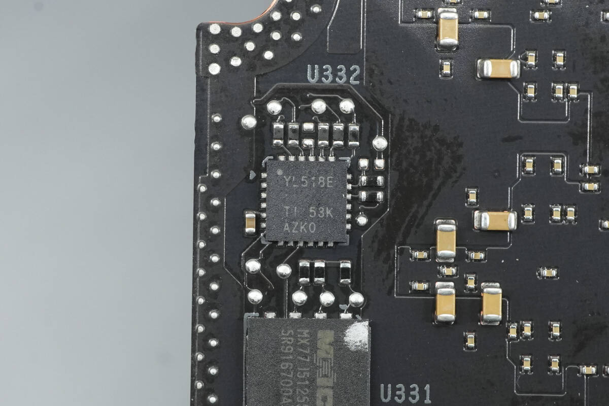
The analog switch is from Texas Instruments, marked with YL518E and identified as TS3A27518E. It is a bidirectional 6-channel 1:2 multiplexer, supporting SD, SDIO, MMC, and QSPI interfaces. The device comes in a WQFN-24 package.
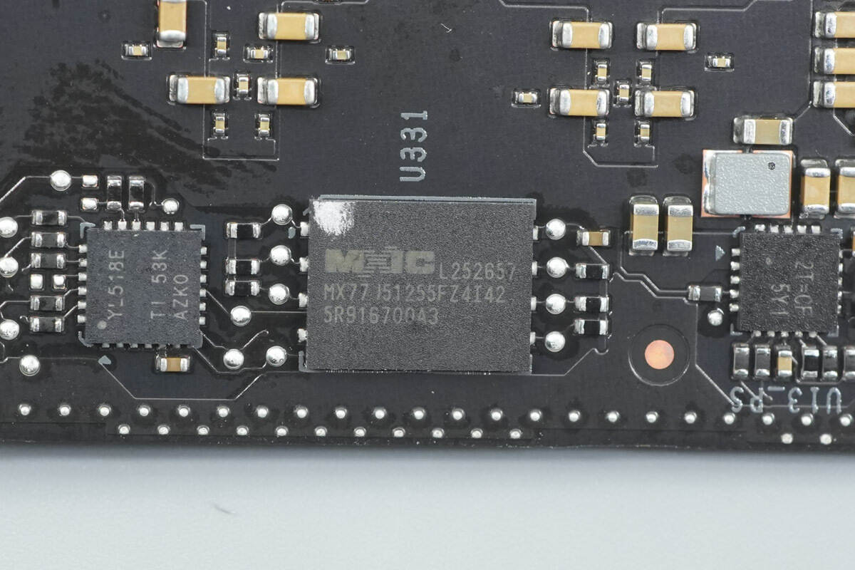
The memory is from MXIC, model MX77U51255FZ4I42. It has a capacity of 512 Mb and comes in an 8-WSON package.
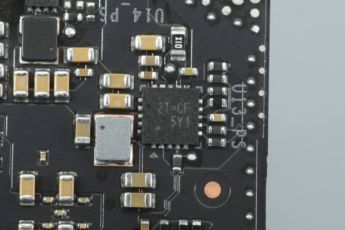
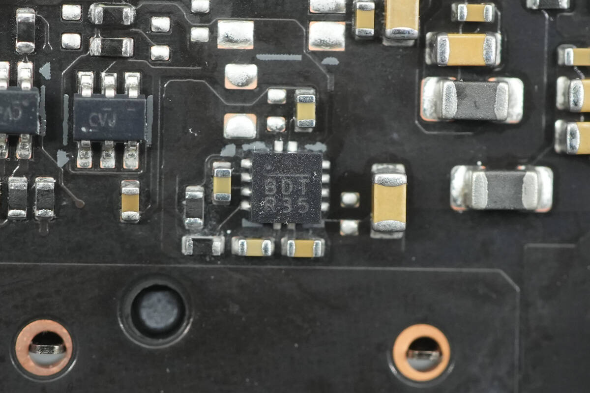
The synchronous buck converter is from RICHTEK, marked with 2T=, model RT8926A, and comes in a QFN32 package.
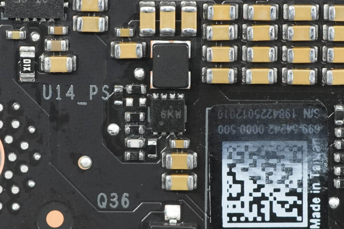
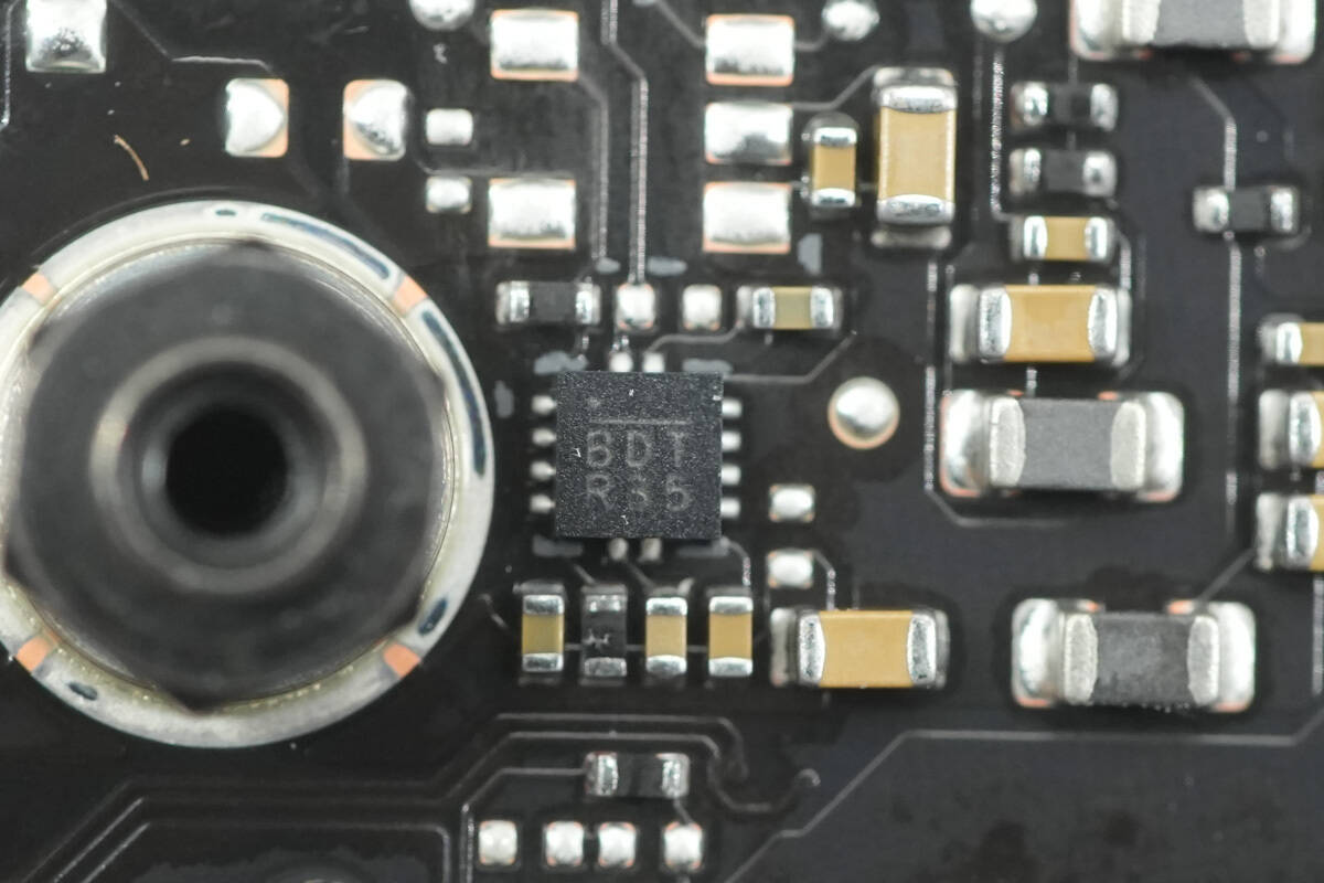
The synchronous buck converter is from RICHTEK, marked with 6KW.
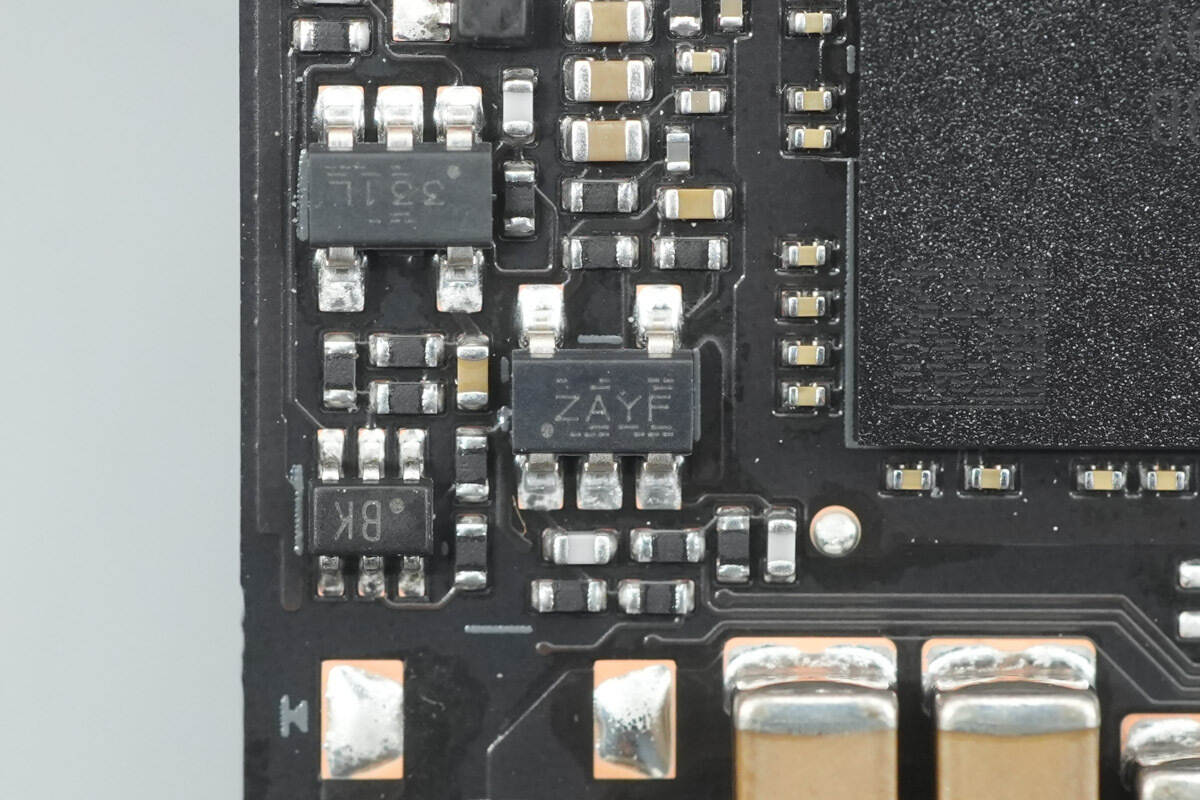
The voltage comparator is from Texas Instruments, marked with ZAYF and identified as TLV1701. It is a micropower comparator supporting a 2.2–36V supply range, and comes in a SOT-23 package.
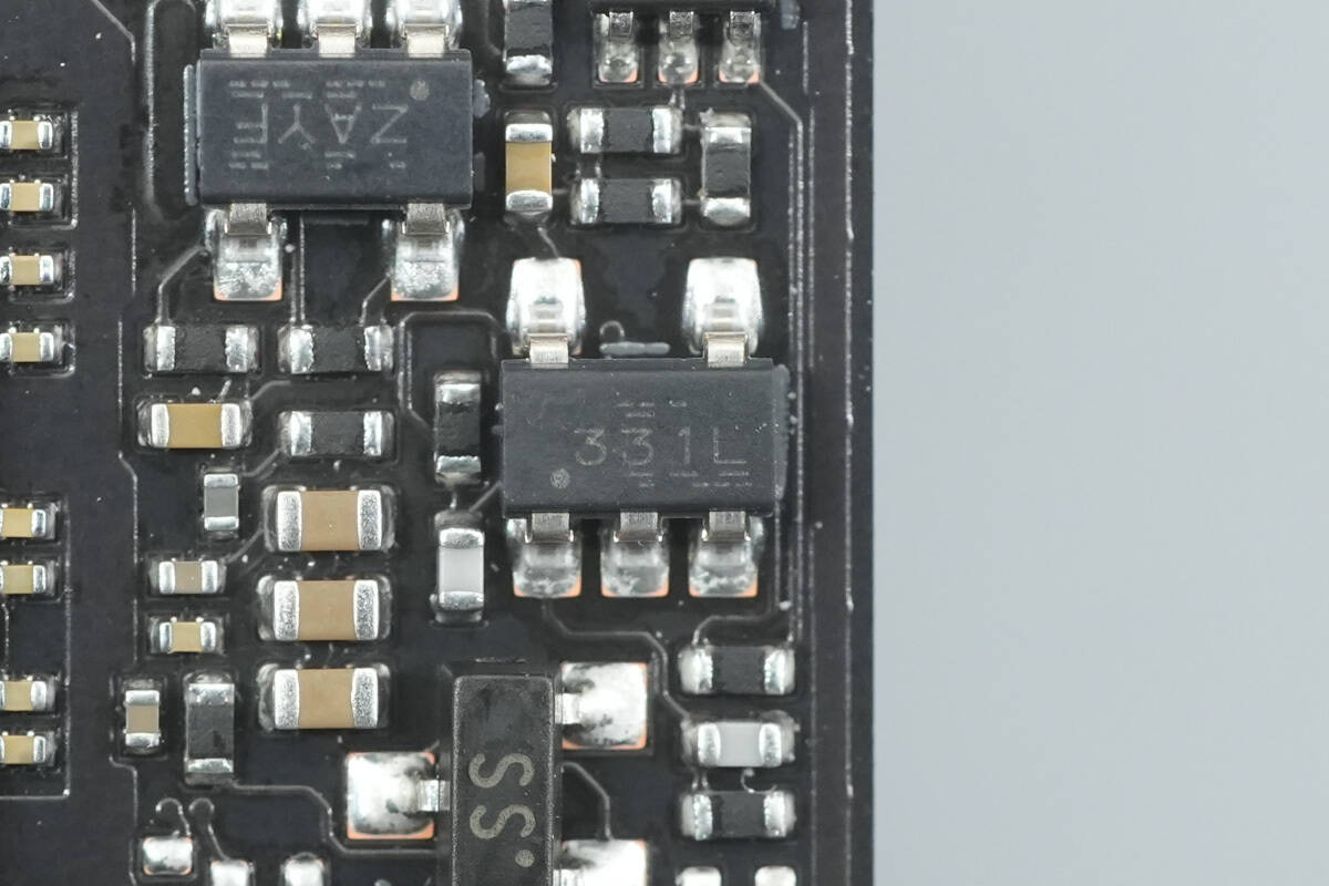
The voltage comparator is from Texas Instruments, marked with 331L and identified as TL331LV. It is a low-voltage standard comparator and comes in a SOT-23 package.
A close-up of the NVIDIA ConnectX-7 network interface controller, protected by a metal top cover. It is marked with K KR 2352 TP1V67 CX07-V000S4N04C-A0. The device supports a maximum aggregate bandwidth of 400 Gb/s and can be configured with 1, 2, or 4 ports.
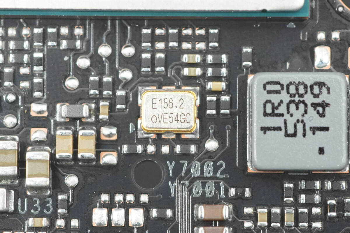
Close-up of the clock crystal oscillator.
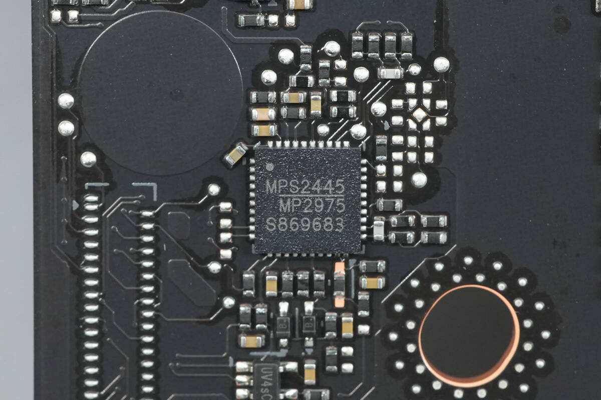
The buck controller is from MPS, model MP2975, and uses a QFN40 package.
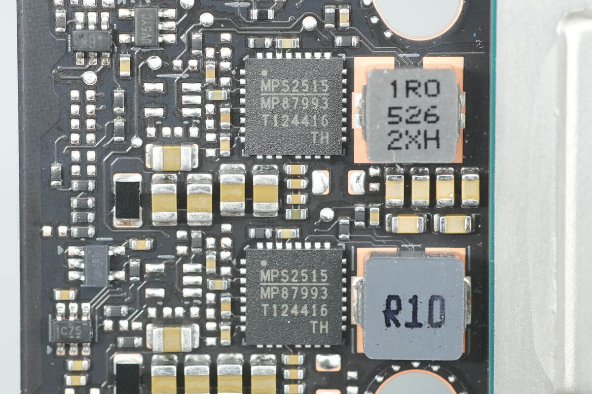
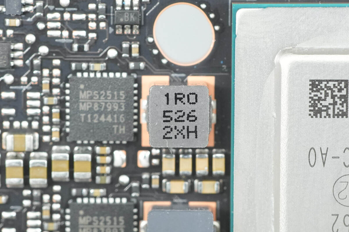
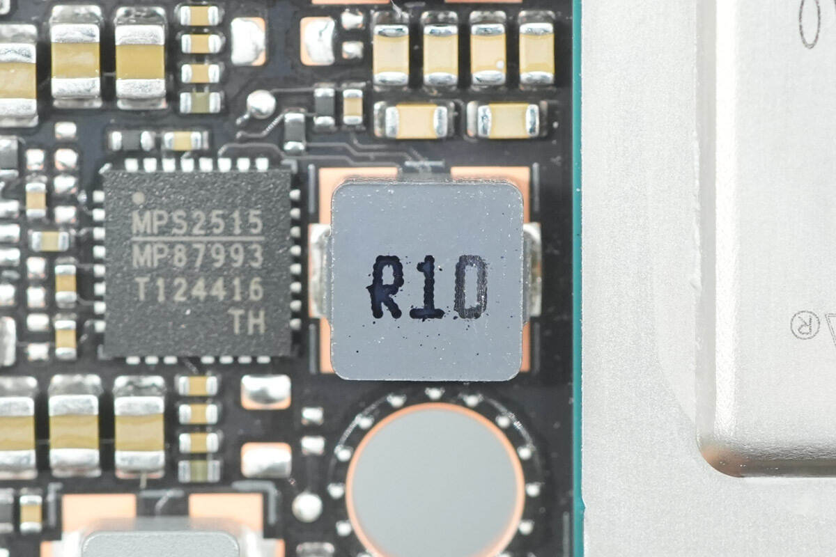
The DrMOS is from MPS, model MP87993, and uses a TLGA5*5 package.
Close-up of a 1μH buck inductor.
Close-up of a 1μH buck inductor.
The synchronous buck chip is from MPS, marked with ADP, model MP1475. It supports a 4.5–16V input voltage range and delivers up to 3A output current. The chip integrates internal switching MOSFETs, operates at a 500 kHz switching frequency, and comes in a TSOT-23-8 package.
Close-up of two 4.7μH buck inductors.
The synchronous buck chip uses MPS MP1475.
Close-up of a 4.7μH buck inductor.
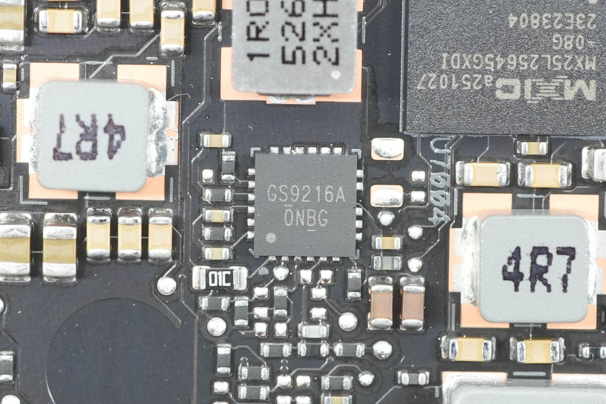
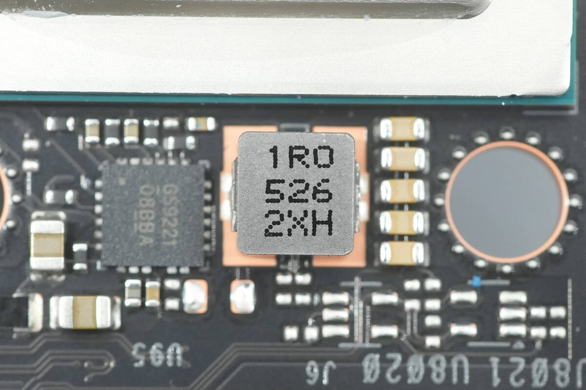
The synchronous buck chip is from GStek, model GS9216A, and uses a TQFN-23 package.
Close-up of a 1μH alloy buck inductor.
The synchronous buck chip uses MPS MP1475.
Close-up of a 4.7μH alloy inductor.
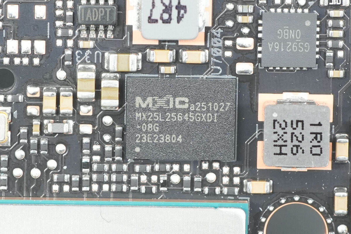
The memory is from MXIC, model MX25L25645GXDI-08G. It has a capacity of 256 Mb and operates within a 2.7–3.6V voltage range. The device comes in a 24-ball BGA package.
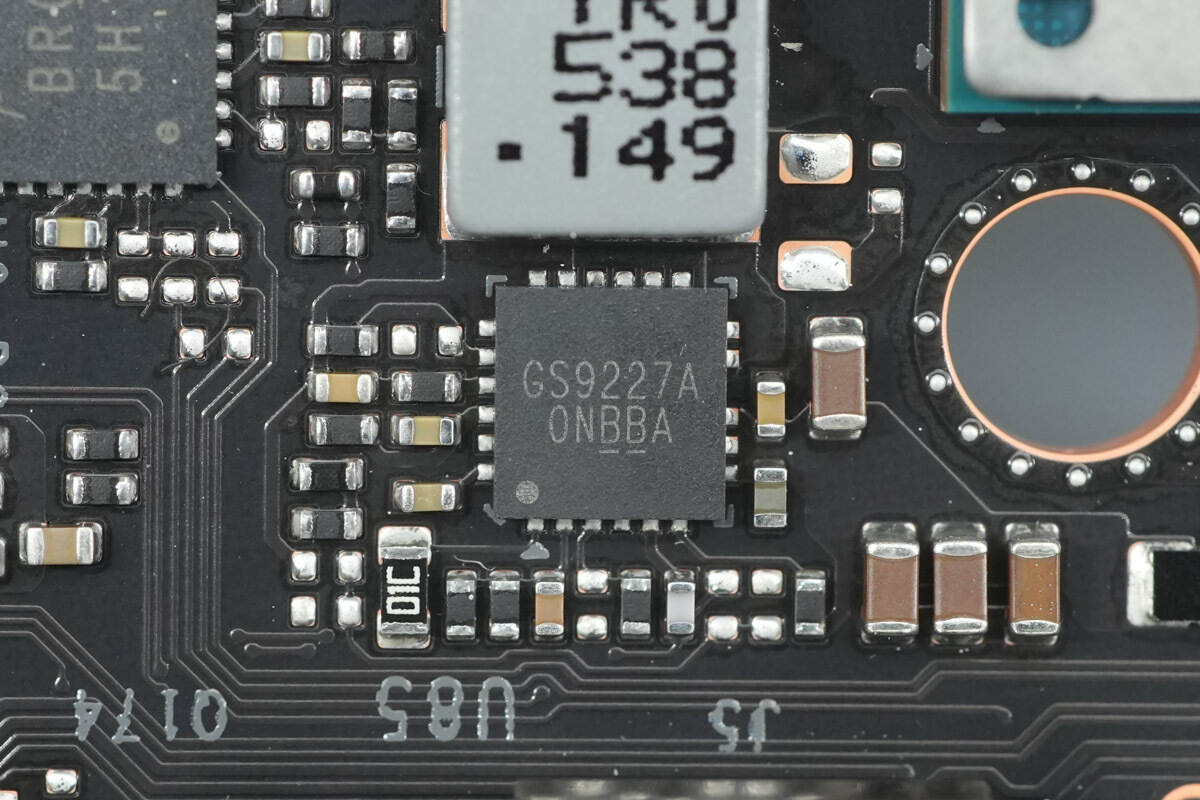
The synchronous buck chip is from GStek, model GS9227A, and uses a TQFN-23 package.
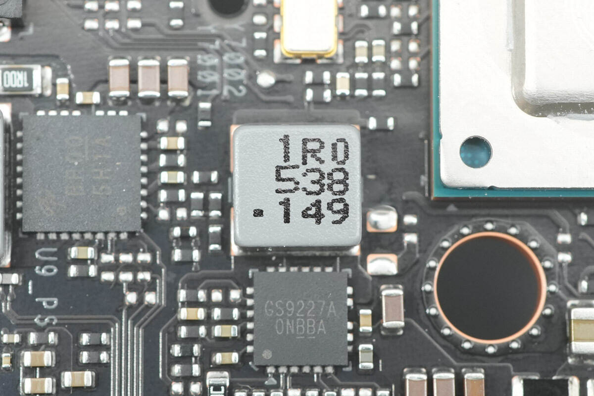
Close-up of a 1μH alloy buck inductor.
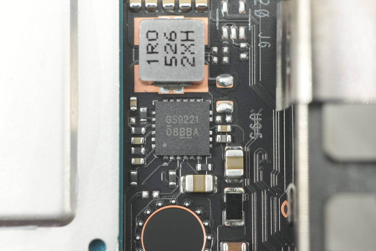
The synchronous buck chip is from GStek, model GS9221. It supports a 2.7–26V input voltage range and a 0.6–12V output voltage range, with up to 6A output current. The device integrates MOSFETs, supports a 100–600 kHz switching frequency, and features overvoltage, undervoltage, overtemperature, and overcurrent protection. It comes in a TQFN-23 package.
Close-up of a 1μH alloy buck inductor.
MLCC capacitors are placed on the back side of the network interface controller for filtering.
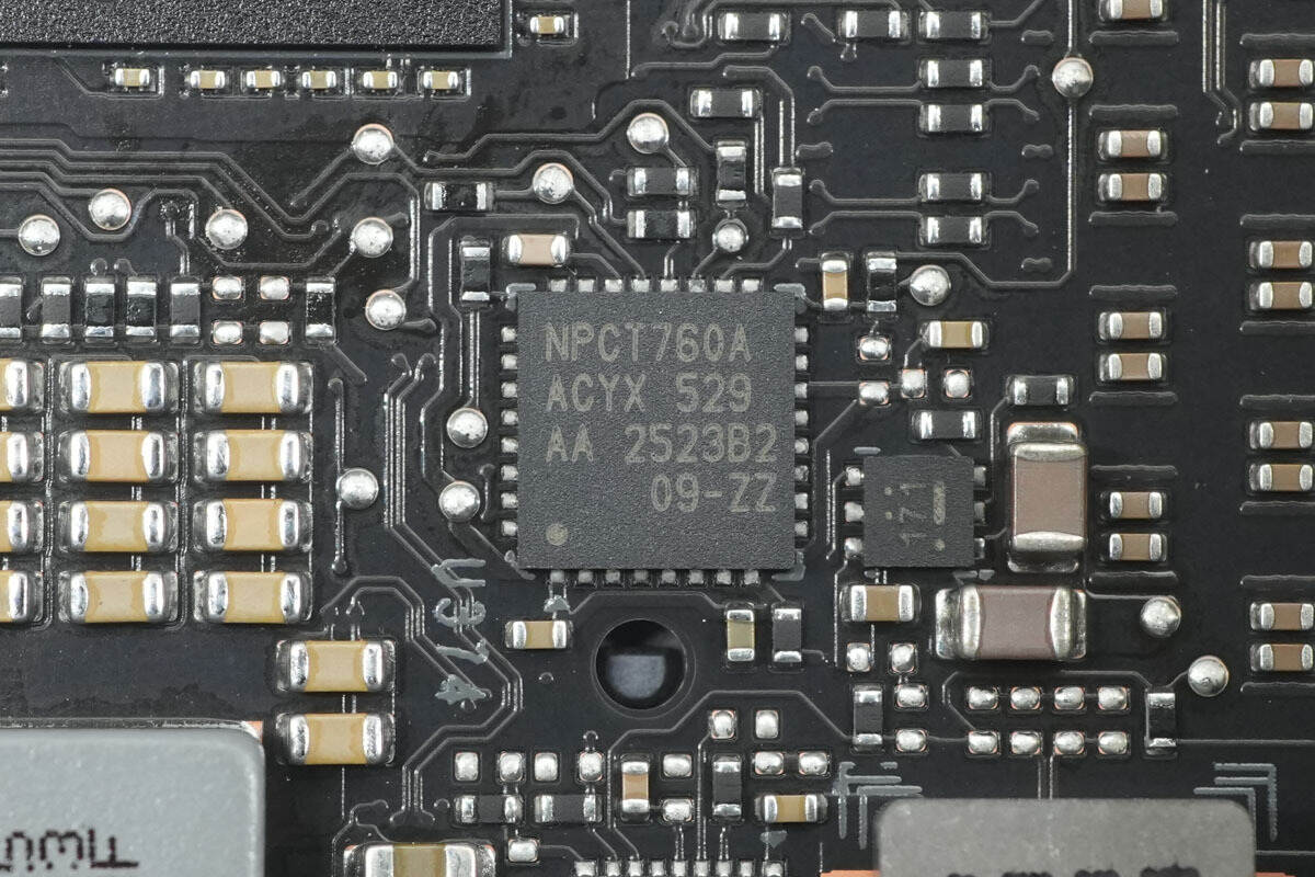
The TPM chip is from Nuvoton, model NPCT760AACYX, and comes in a QFN-32 package.
The load switch is from RICHTEK, marked with 17 and identified as RT9728AHZQW. It supports a 2.5–5.5V operating voltage range and a 75 mA–1.3 A current limit. The device integrates a 120 mΩ high-side switch and comes in a WDFN-6L package.

The PMIC is from MediaTek, model MT6363CFW.
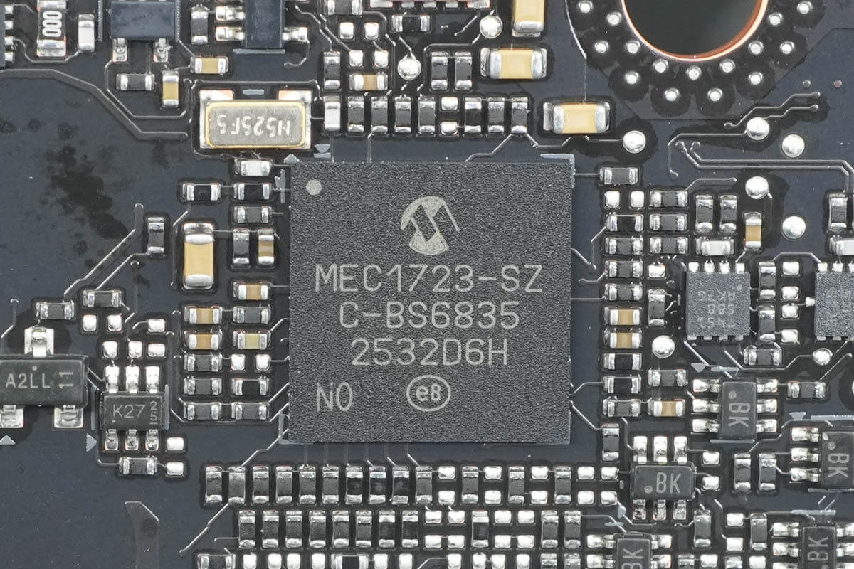
The EC chip is from Microchip, model MEC1723. It integrates an ARM Cortex-M4F embedded processor, supports eSPI and I²C interfaces, and comes in a 144-pin WFBGA package.
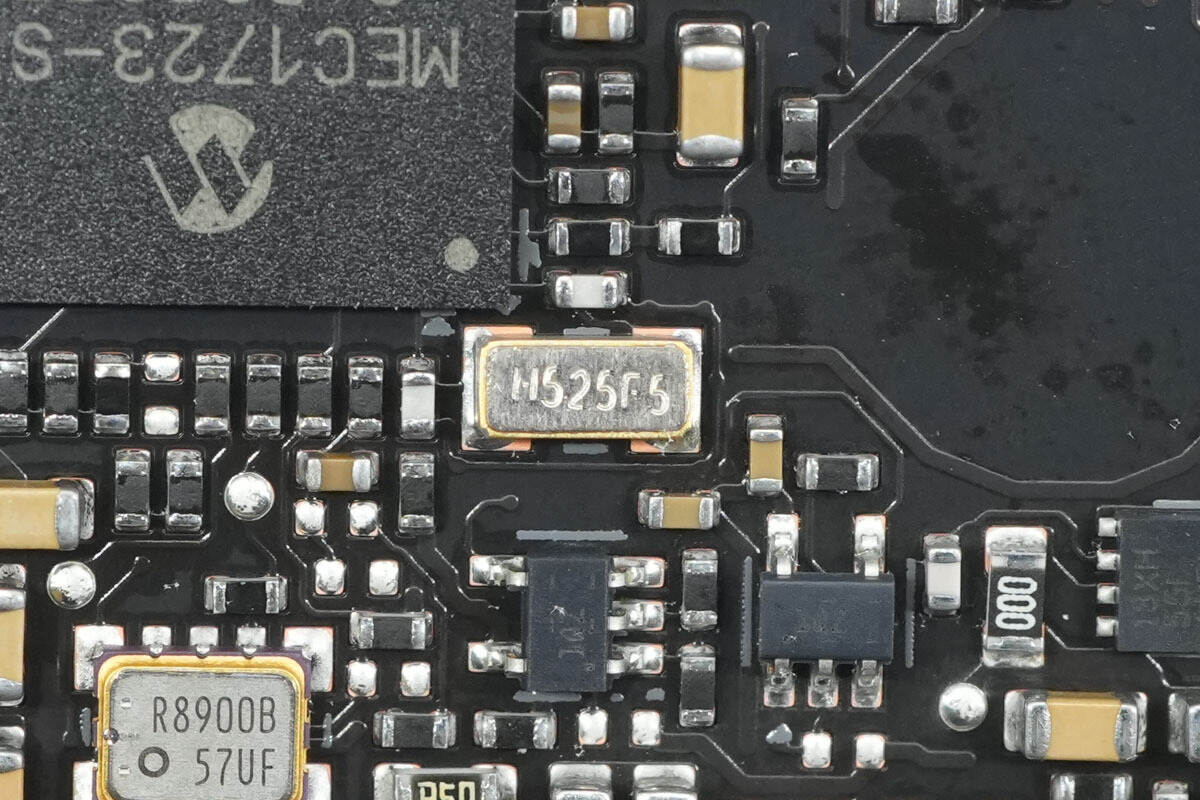
Close-up of an SMD crystal oscillator.
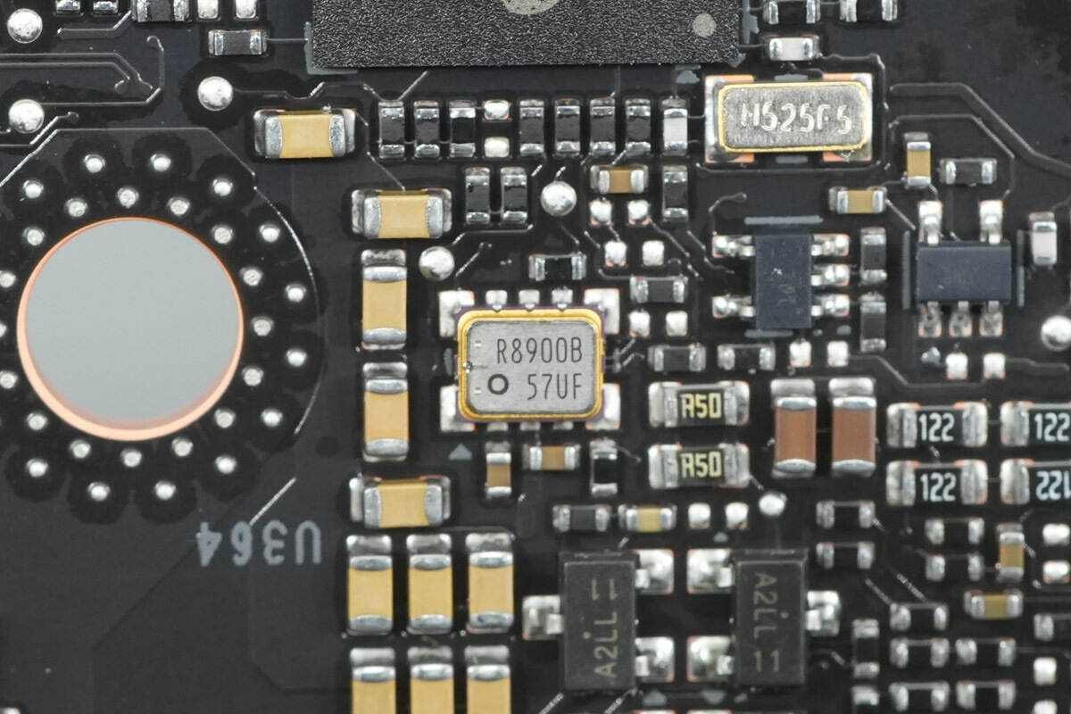
The real-time clock module is model RA8900CE. It integrates a 32.768 kHz clock and a digitally temperature-compensated crystal oscillator, and supports an I²C interface.
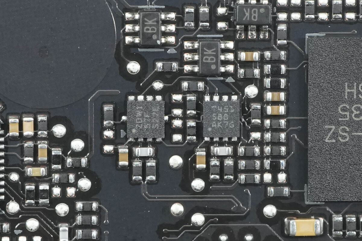
The left digital temperature sensor is from Texas Instruments, marked with ZDW1 and identified as TMP461. It is a high-accuracy remote and local temperature sensor with a pin-programmable bus address, integrating an internal local temperature sensor. The device supports an SMBus interface and comes in a WQFN-10 package.
The right digital temperature sensor is marked with T451 and identified as TMP451. It is a high-accuracy, low-power remote temperature sensor monitor with an integrated local temperature sensor. It also supports an SMBus interface and comes in a WSON-8 package.
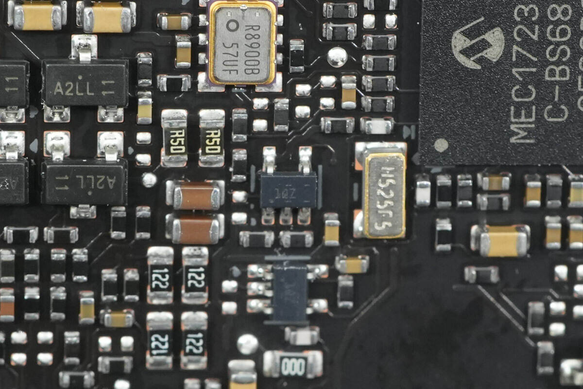
The logic AND gate is from Texas Instruments, marked with 1QZ and identified as SN74LV1T08. It is a single-supply 2-input positive AND gate with integrated logic level shifting, and comes in a SOT-23 package.
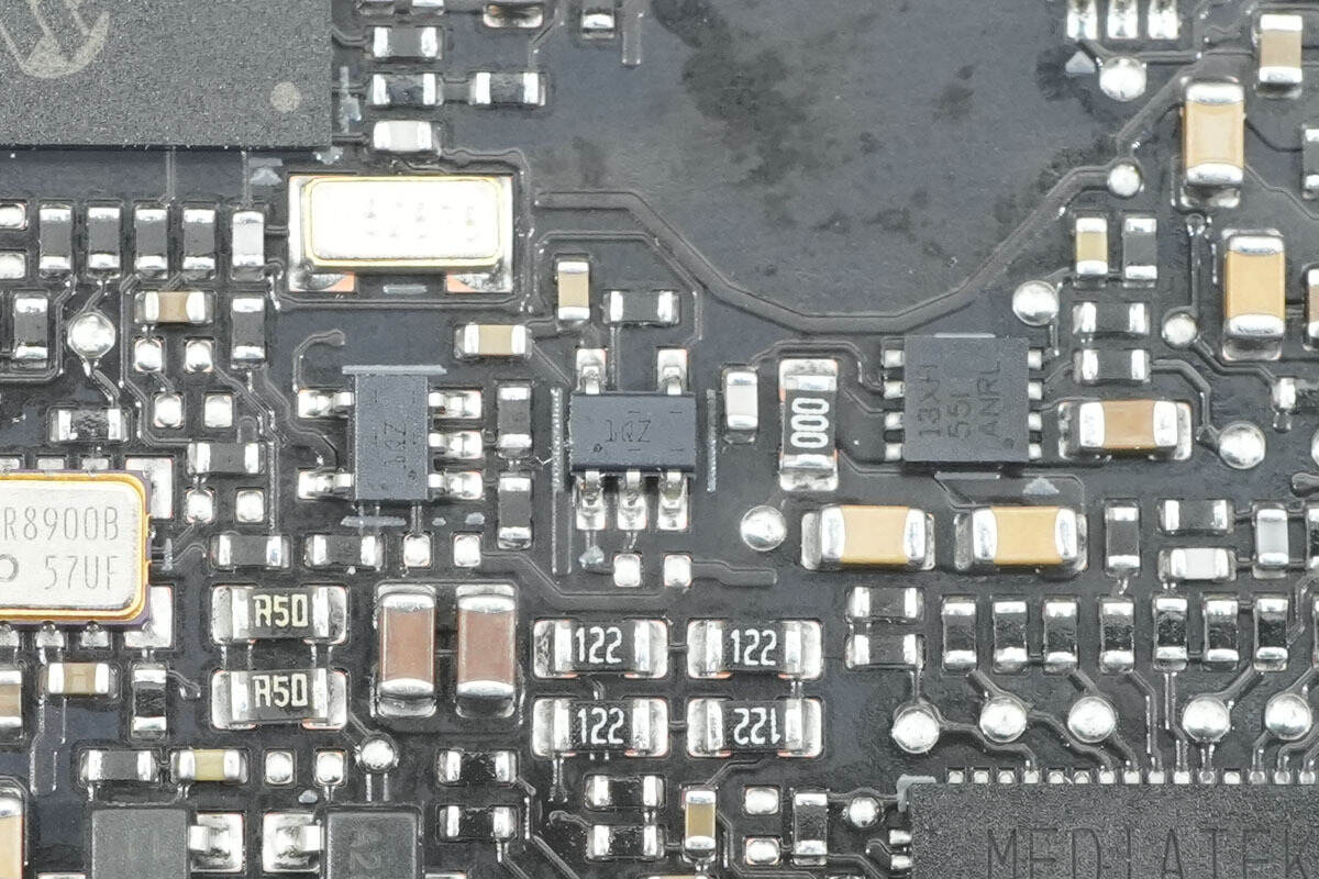
The second AND gate IC is of the same model.
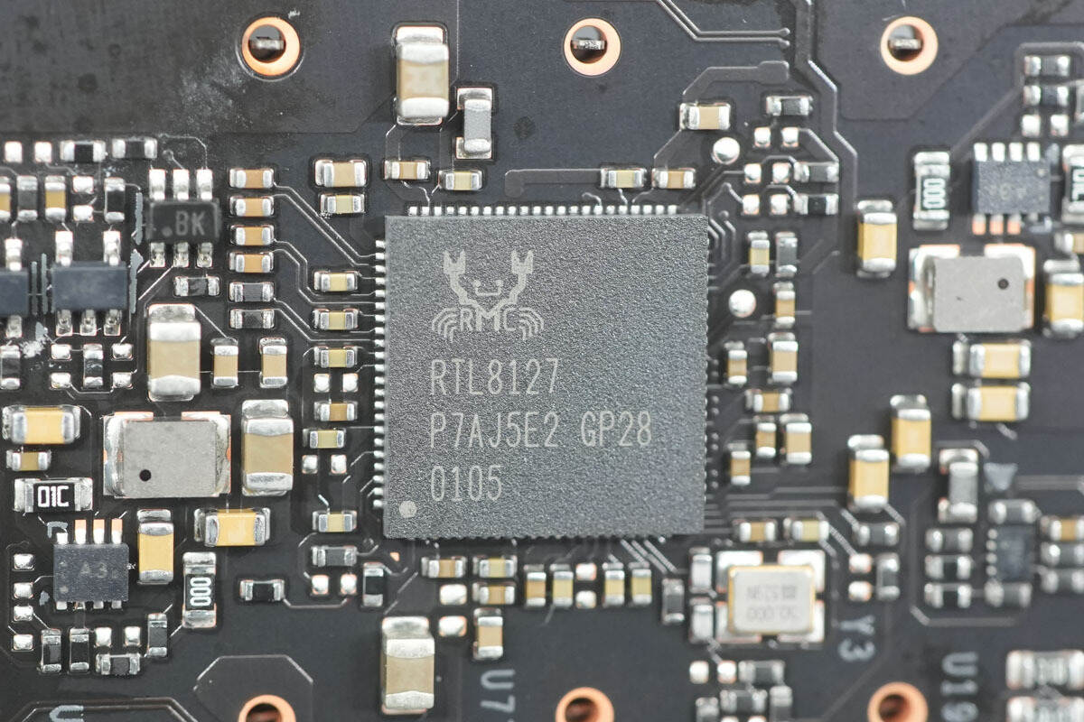
The network interface controller is from REALTEK, model RTL8127. It supports a 10 Gbps data rate and is backward compatible with 10M/100M/1G/2.5G/5G speeds. The device supports a PCIe Gen4 interface and comes in a QFN-88 package.
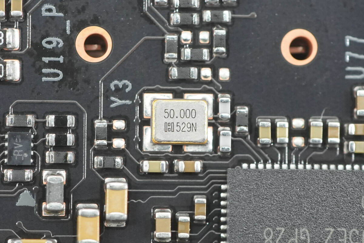
Close-up of a 50.000MHz clock crystal oscillator.
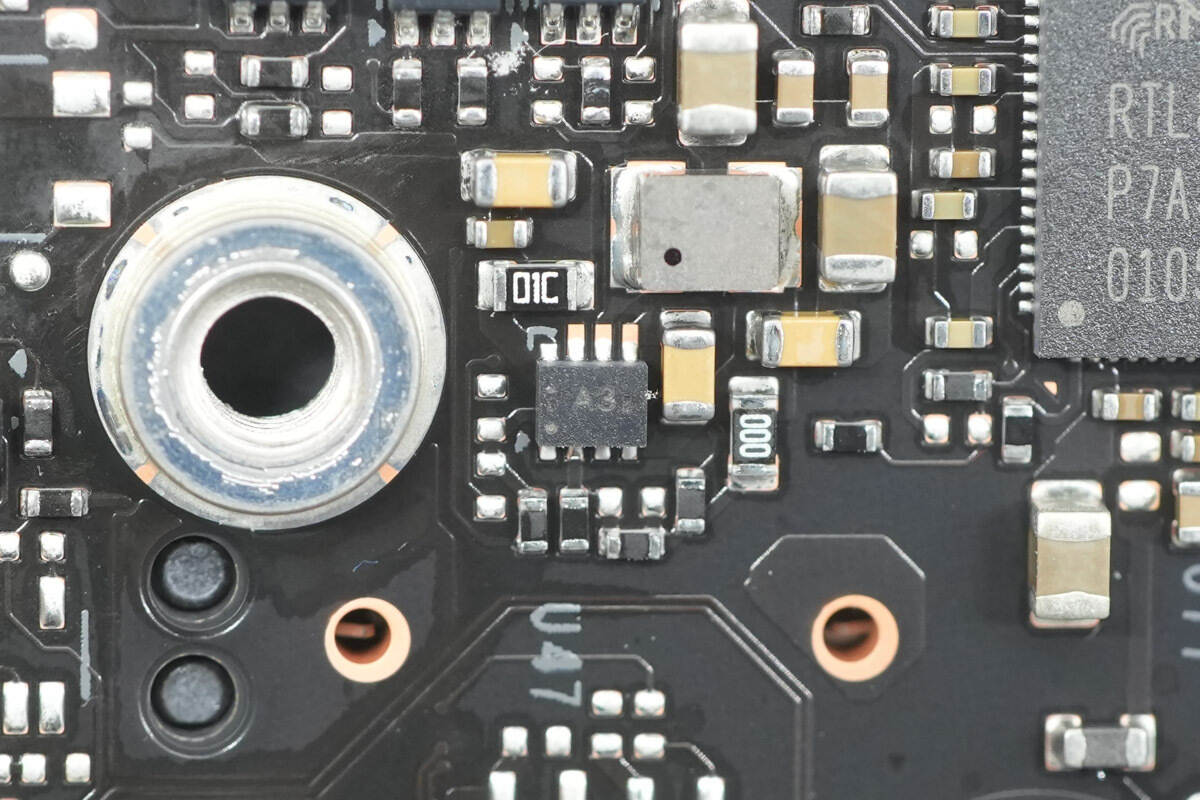
The synchronous buck chip is marked with A3.
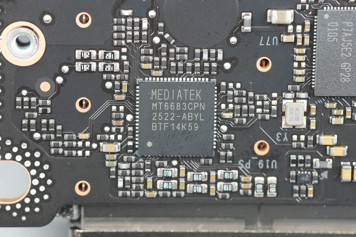
The chip marked with MT6683CPN is from MediaTek.
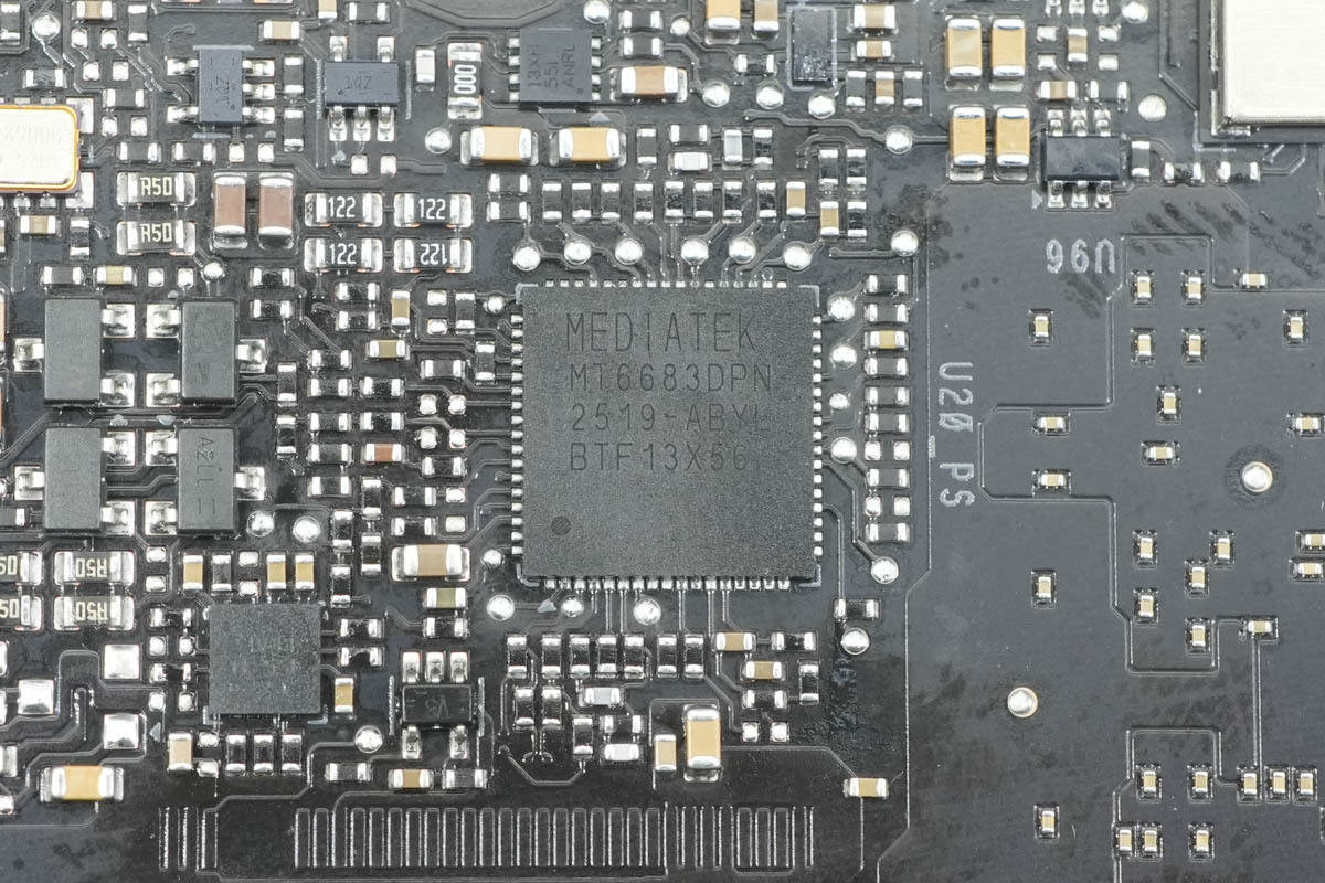
The chip marked with MT6683DPN is from MediaTek.
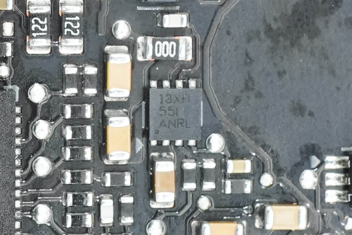
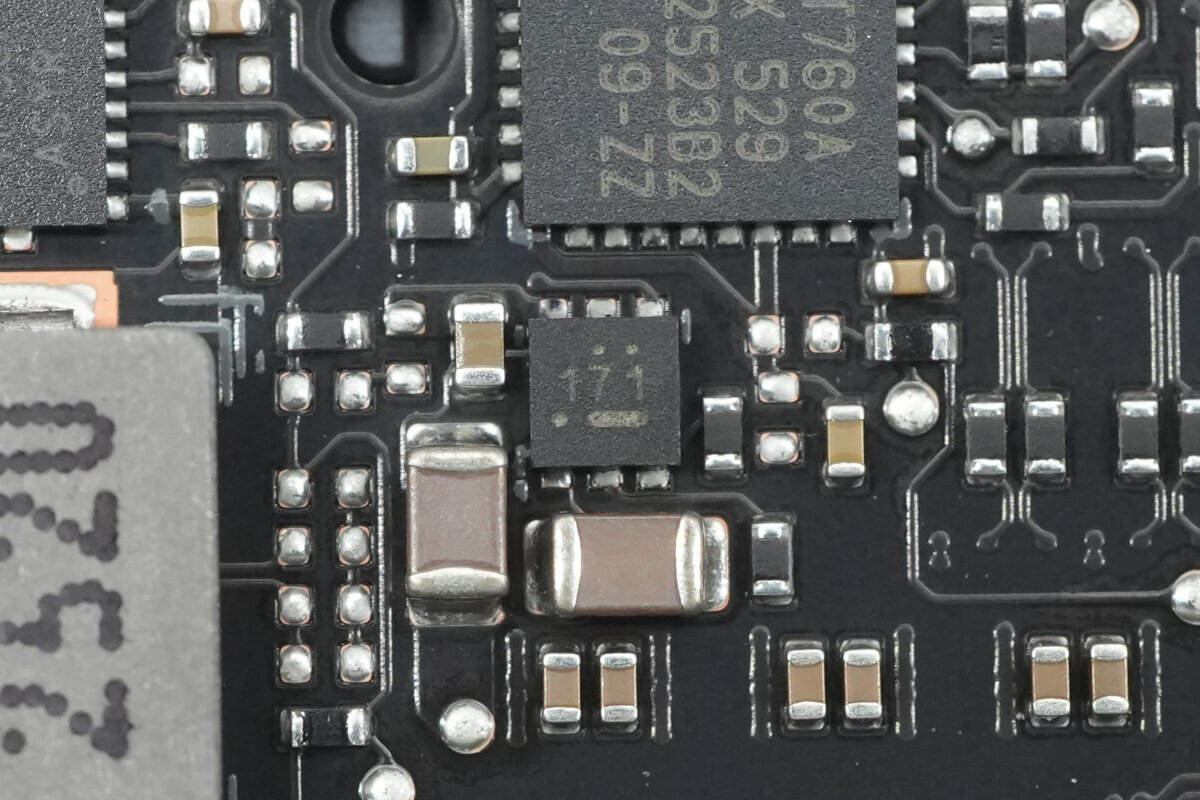
The load switch is from Texas Instruments, marked with 13XH and identified as TPS22975. It is a 5.7V, 6A load switch with 16 mΩ on-resistance, featuring adjustable rise time, selectable output discharge, and thermal shutdown protection. The device comes in a WSON-8 package.
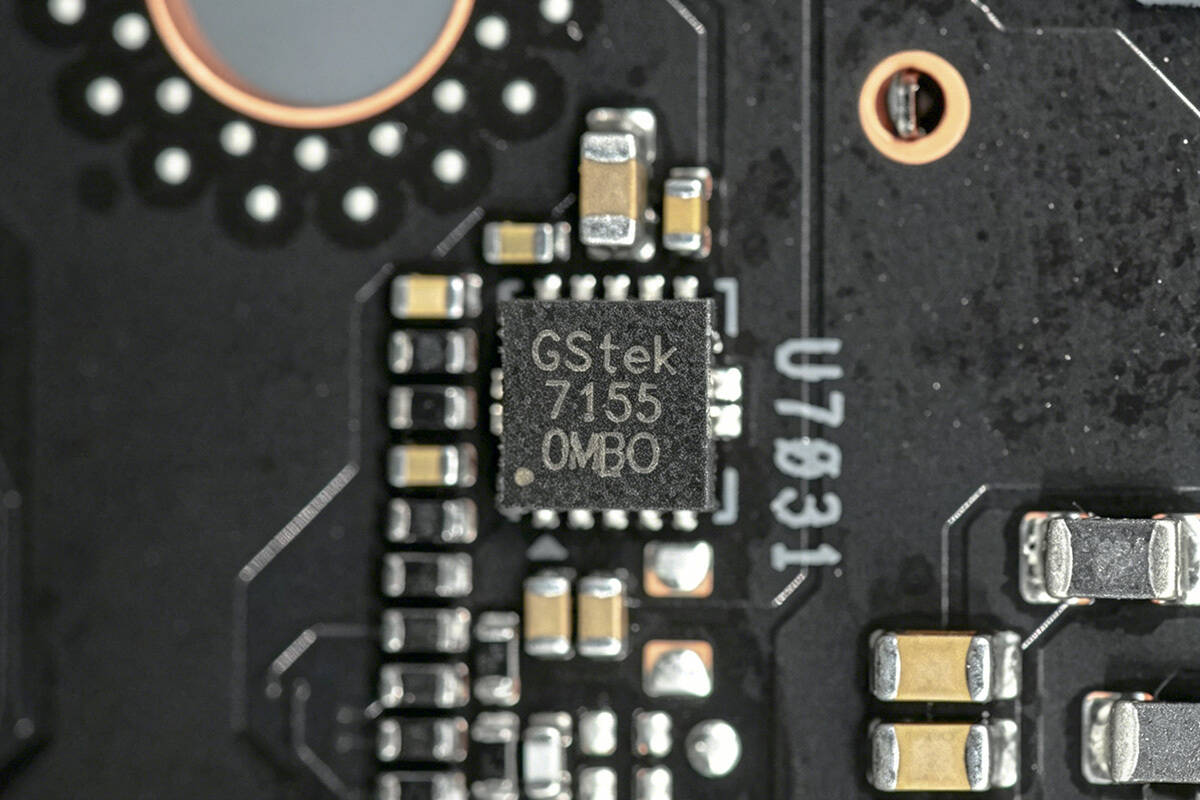
The voltage regulator is from GStek, model GS7155. It is a low-dropout regulator with up to 3A output current and comes in a TDFN-10 package.
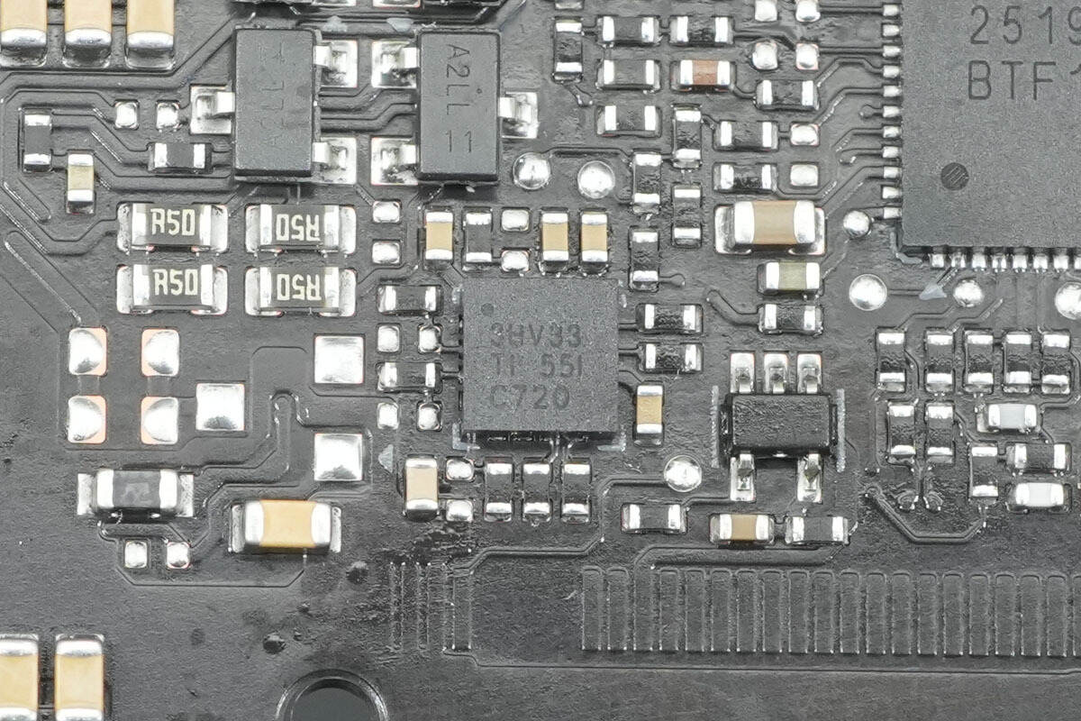
The clock generator is from Texas Instruments, marked with 3HV33 and identified as LMK3H0102. It is a programmable BAW clock generator with no external reference required, supporting 2 differential or 5 single-ended outputs. The device is compatible with PCIe Gen1 to Gen7 standards, integrates an internal BAW resonator, and comes in a TQFN-16 package.
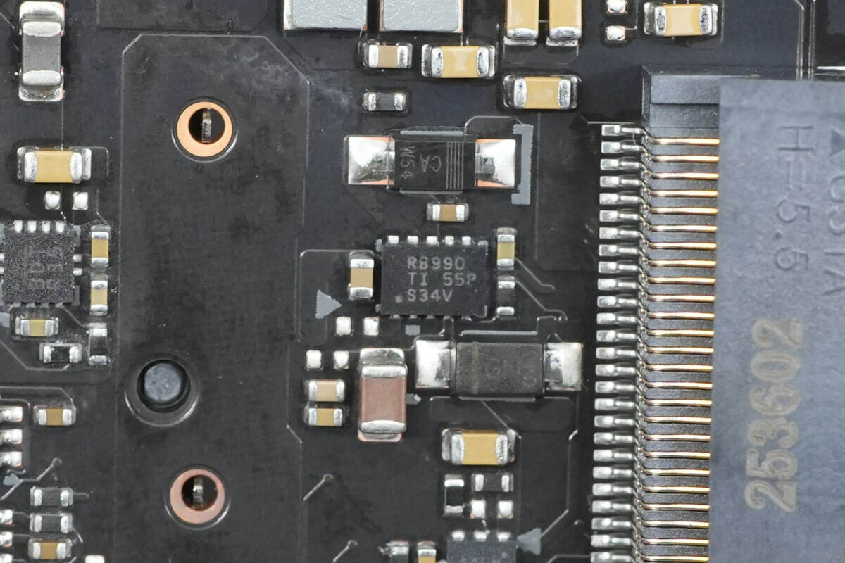
The load switch is from Texas Instruments, marked with RB990 and identified as TPS22990. It is a 5.5V, 10A load switch with 3.9 mΩ on-resistance, featuring adjustable rise time, power-good indication, and optional output discharge. The device comes in a WSON-10 package.
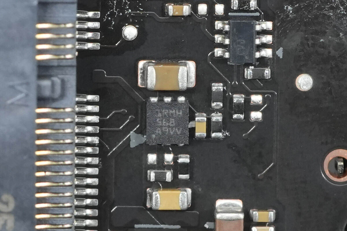
The voltage regulator is from Texas Instruments, marked with 1RMH and identified as TLV76701. It supports a 2.5–16V input voltage range and delivers up to 1A output current. The device is a precision linear regulator and comes in a WSON-6 package.
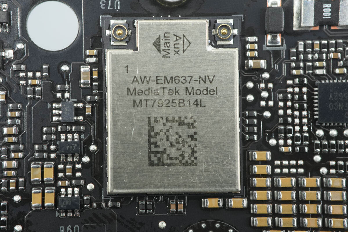
The wireless network module, model AW-EM637-NV, integrates a MediaTek MT7925 chipset.
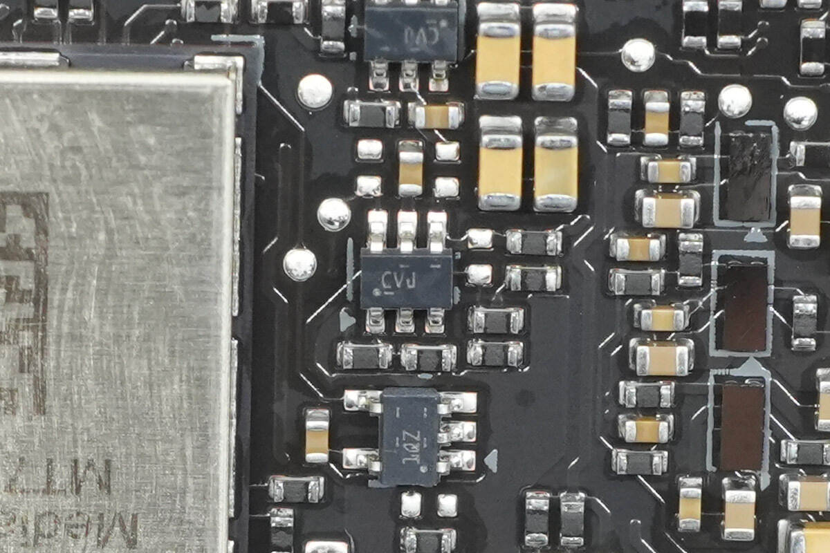
The buffer is from Texas Instruments, marked with CVJ and identified as SN74LVC1G07. It is a single-channel buffer with open-drain output, supporting a 1.65–5.5V operating voltage range, and comes in a SOT-23 package.
The load switch is from MPS, marked with BD and identified as MP5087. It supports a 0.5–5.5V operating voltage range and up to 7A load current, and comes in a QFN-12 package.
The other load switch is of the same model.
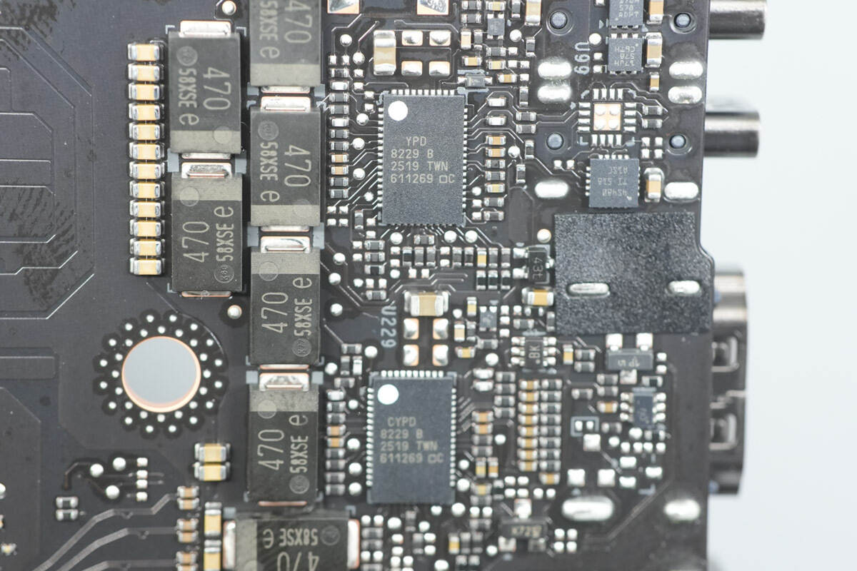
The USB-C interface controller is from Infineon, model CYPD8229, belonging to the EZ-PD CCG8 CFP series. It supports dual USB-C port control and integrates a Cortex-M0+ processor, along with 128 KB Flash and 96 KB ROM. The device supports USB PD 48V applications and comes in a 52-pin QFN package.
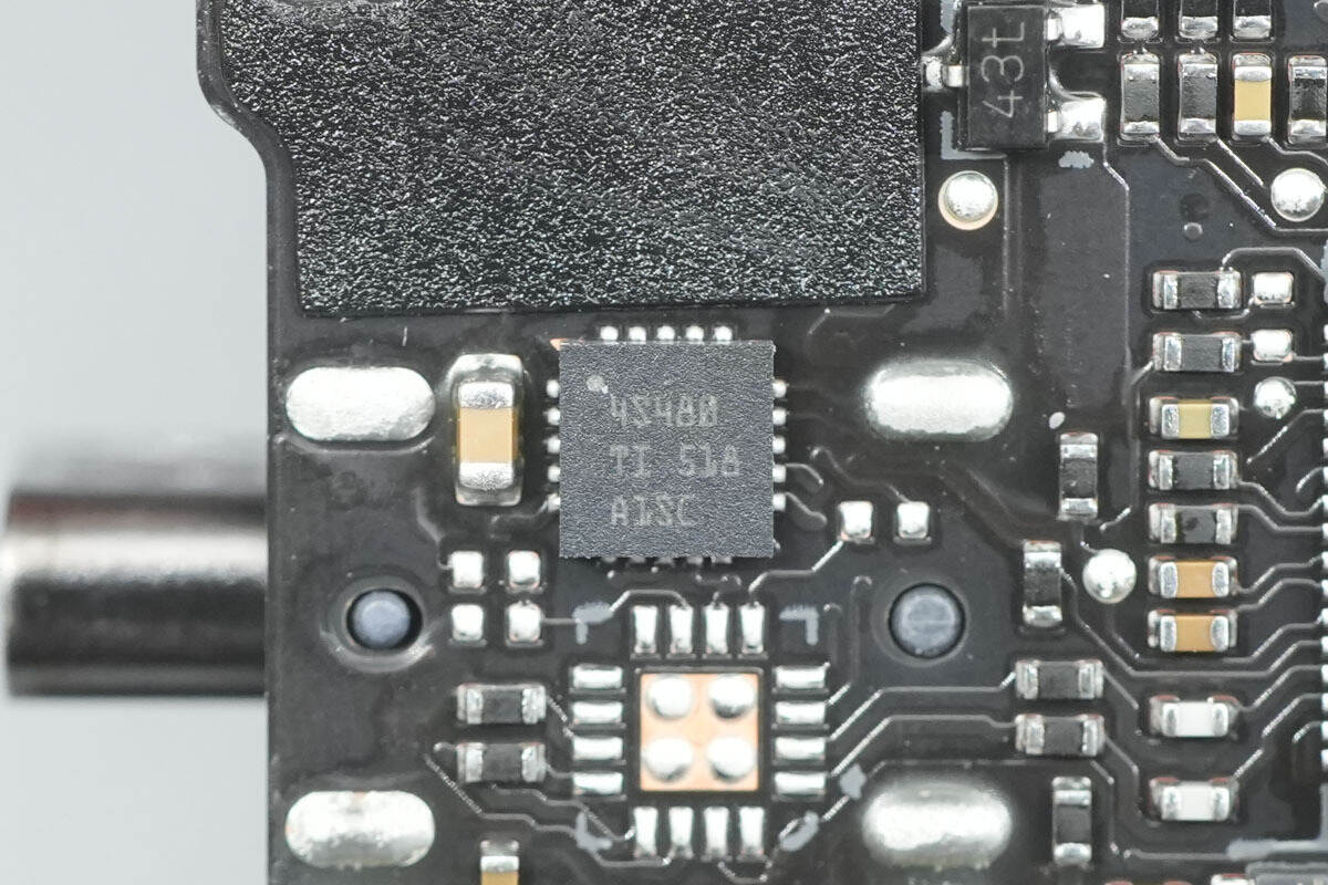
The port protection device is from Texas Instruments, marked with 4S480 and identified as TPD4S480. It is a USB-C 48V EPR port protection device featuring VBUS short-to-overvoltage protection and IEC ESD protection. It provides overvoltage and ESD protection for CC1, CC2, SBU1, and SBU2 pins, and comes in a WQFN-20 package.
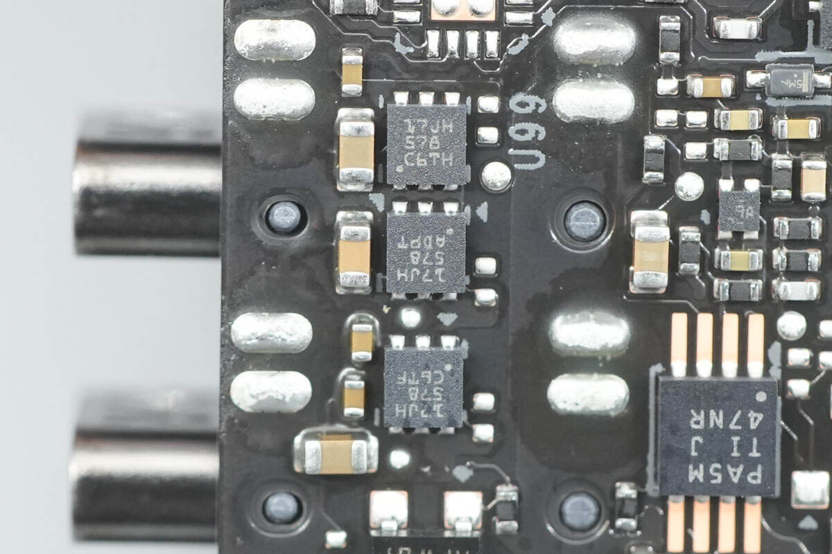
The surge protection devices are from Texas Instruments, marked with 17JH and identified as TVS3300. It is a 33V flat-clamp surge protection device featuring low leakage current and low capacitance, and comes in a SON-6 package.
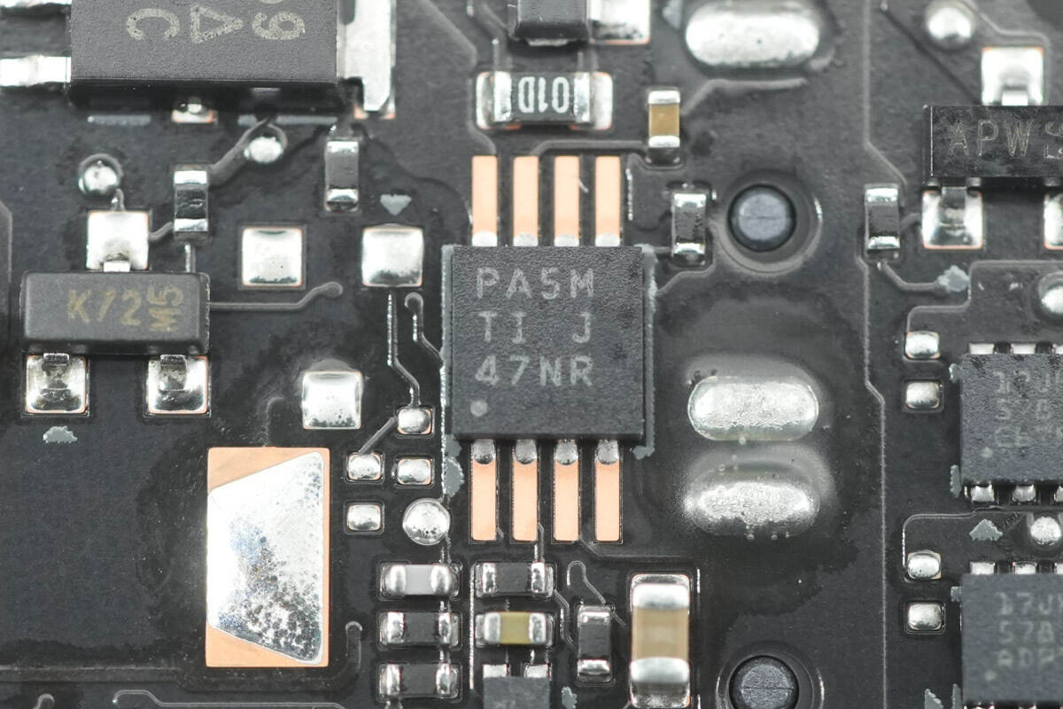
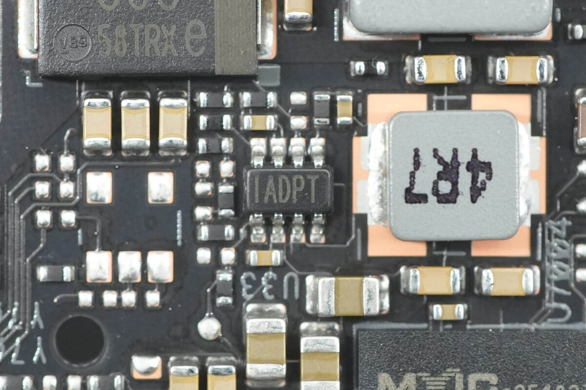
The voltage regulator is from Texas Instruments, marked with PA5M and identified as TPS7A1601. It supports a 3–60V input voltage range, features a 5 μA quiescent current, and provides up to 100 mA output current. The device is a linear regulator and comes in a VSON-8 package.
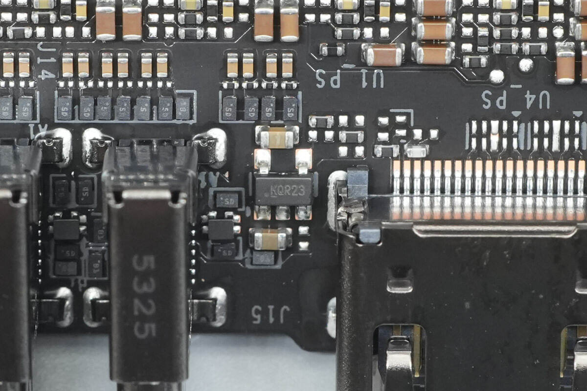
A close-up of a chip marked with KQR23.
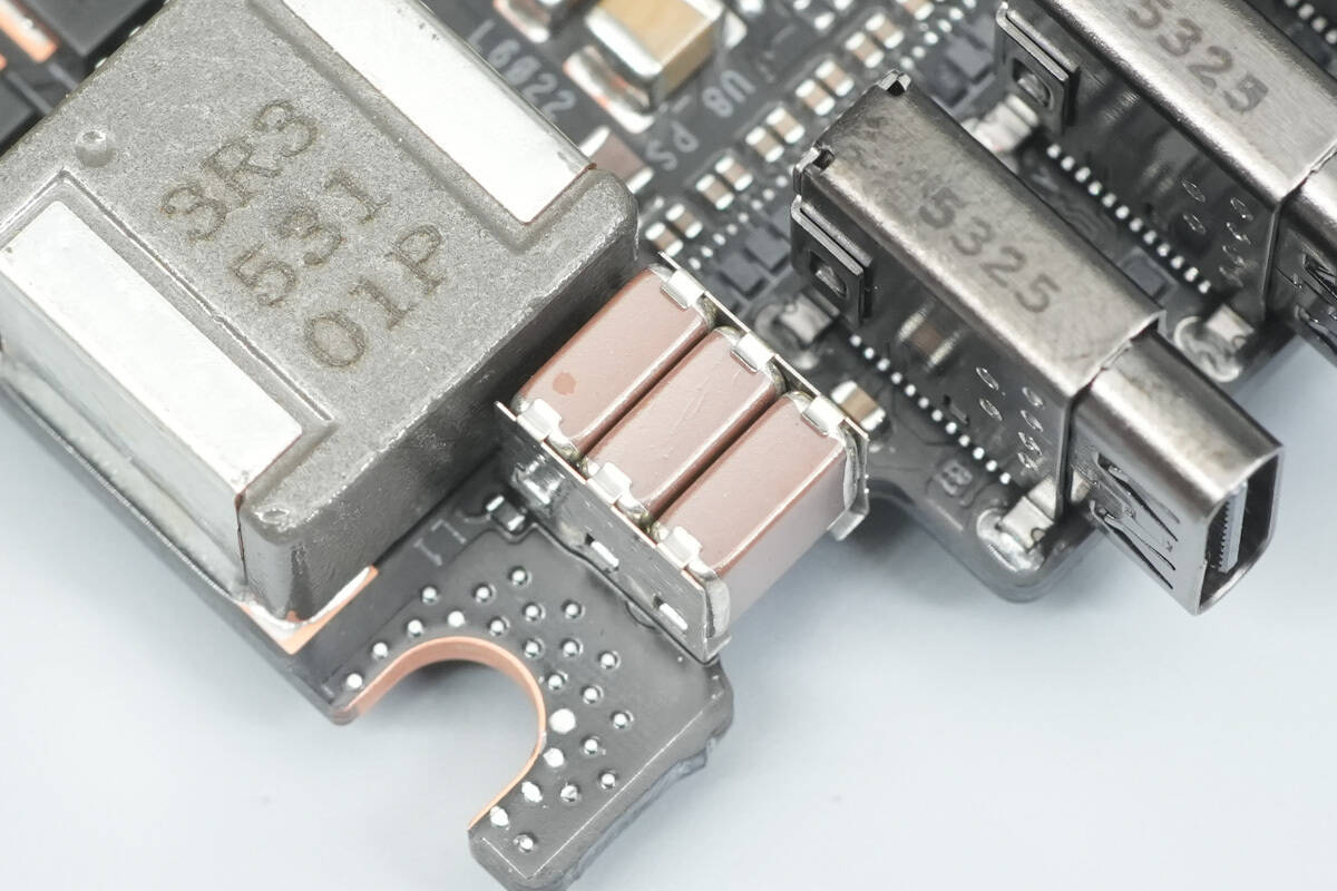
The USB-C sockets are secured using through-hole soldering, and TVS diodes are used for overvoltage protection.
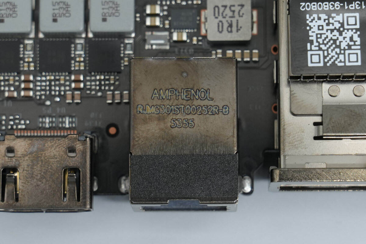
A close-up of the 10GbE network interface.
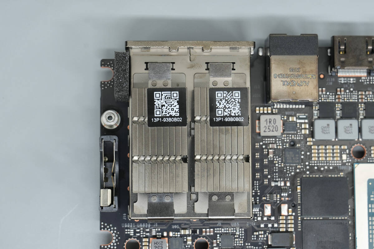
A close-up of the heatsink fins above the QSFP interface.

Well, those are all components of the NVIDIA DGX Spark 4TB.
Summary of ChargerLAB
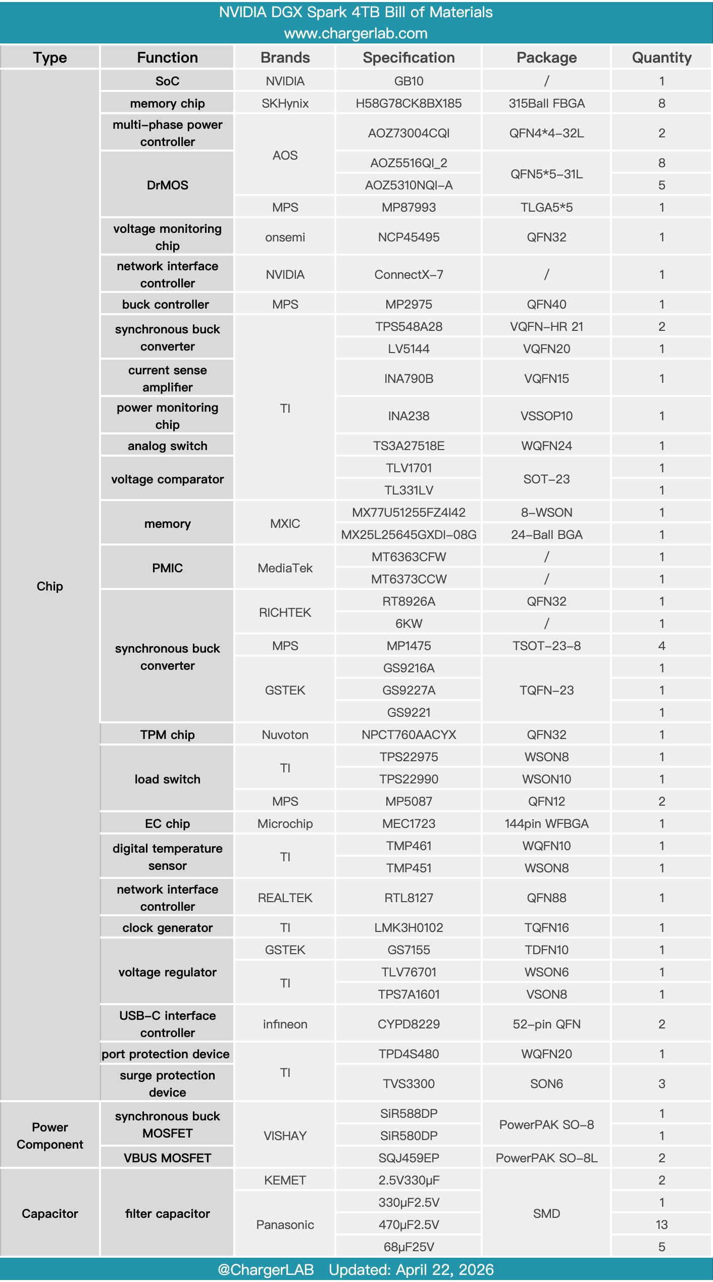
Here is the component list of the NVIDIA DGX Spark 4TB for your convenience.
It uses an aluminum alloy enclosure in an SFF form factor. The rear panel is equipped with four USB-C ports, an HDMI interface, a 10GbE network port, and two QSFP ports. The server is powered by a PD 3.1 power supply with a 48V 5A rating.
After taking it apart, we found that the PCBA module is found to be secured to the enclosure via an aluminum alloy baseplate, with the heatsink mounted directly on it. Inside, the system integrates a GB10 superchip, surrounded by eight SKHynix LPDDR5X memory chips on the left and right sides. On the top and bottom sides, there is an Alpha & Omega Semiconductor AOZ73004CQI multiphase power controller, along with AOZ5516QI_2 and AOZ5310NQI-A DrMOS devices.
The ConnectX-7 network interface is powered by an MPS MP2975 controller paired with MP87993 DrMOS. The EC chip uses Microchip MEC1723, while the TPM module uses Nuvoton NPCT760AACYX. The input power stage uses a Texas Instruments LV5144 synchronous buck controller combined with VISHAY MOSFETs. The USB-C controller is an Infineon CYPD8229, supported by Texas Instruments protection ICs.
At the bottom of the system, there is a 2242 M.2 SSD slot, with the 4TB configuration pre-installed with a Samsung PM9E1 SSD. Thermal design includes a vapor chamber for the GB10 chip, heat pipes for the network controller and DrMOS stages, and thermal pads applied across memory, DrMOS, wireless module, and SSD to ensure stable and reliable operation.
Related Articles:
1. Teardown of Apple USB‑C to Apple Pencil Adapter (A2869)
2. Teardown of Xiaomi 33W USB-A Charger (MDY-16-EF)
3. Teardown of SHARGE HyperTower 170W Power Bank (X6)