Introduction
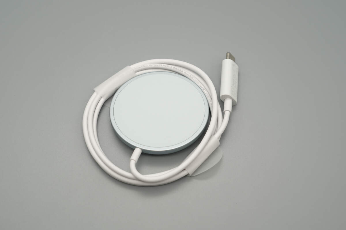
We have got a wireless charger from Google that comes with a built-in 1-meter USB-C cable. The wireless charging panel features a magnetic function, providing the same magnetic charging experience as Apple’s MagSafe charger.
Another key highlight is its support for the latest Qi 2.2 wireless charging standard, offering up to 25W fast wireless charging. It not only meets the wireless charging needs of devices like the Google Pixel 10 Pro XL but also works well with the iPhone 17 series and Xiaomi 17 series. Below, we will perform a teardown to take a closer look at its specific design.
Product Appearance
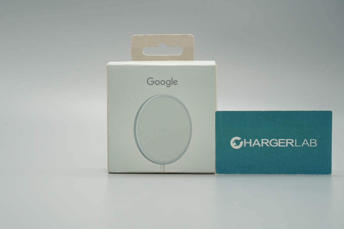
The front of the packaging features the Google logo and an image of the product.
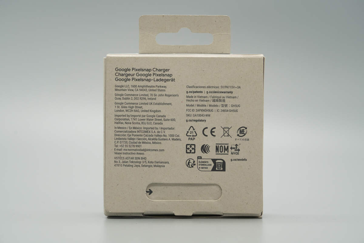
The back of the packaging displays the product model, specifications, certifications, and other related information.
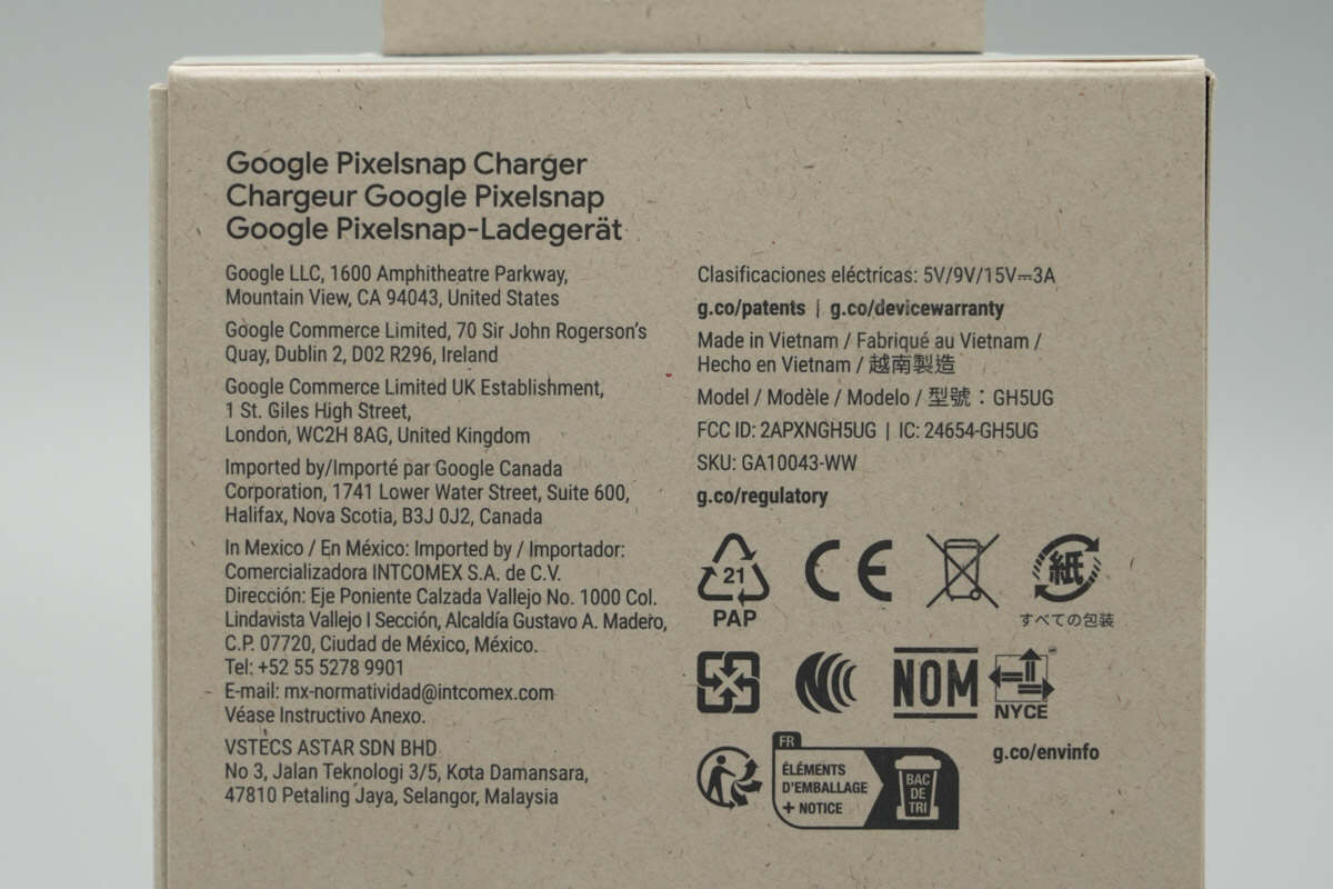
It has obtained CE, NOM, and NYCE certifications.
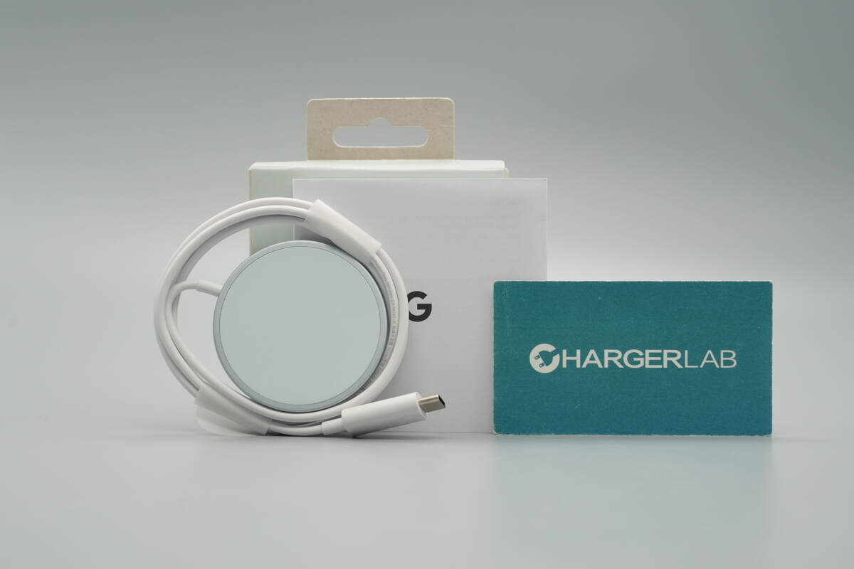
The package includes the wireless charger and a user manual.
The built-in USB-C cable is secured with plastic film.
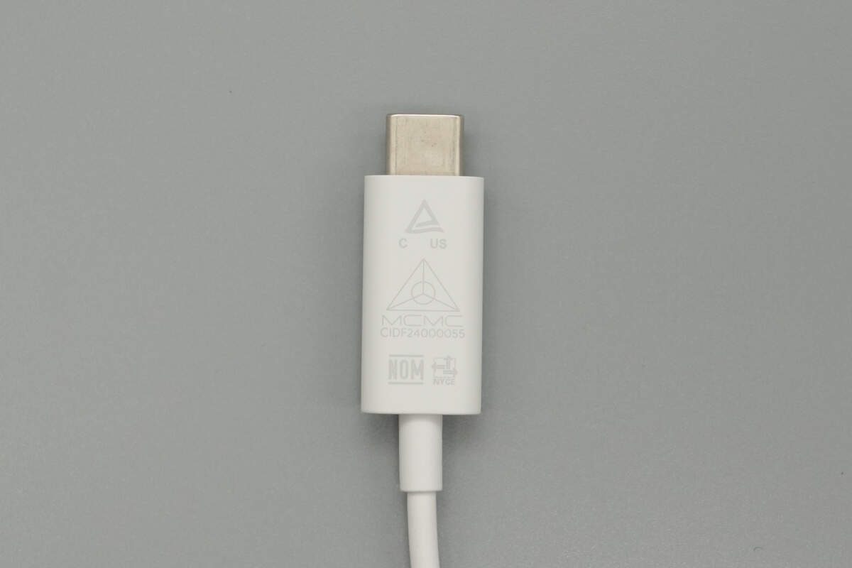
The USB-C connector housing is made of PC flame-retardant material with a matte finish. The front side is printed with certification marks such as NOM and NYCE.
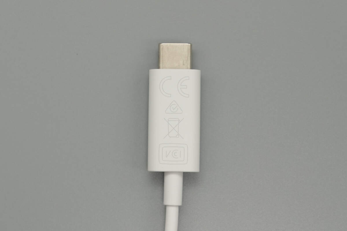
The other side is printed with certification marks, including CE and VCCI.
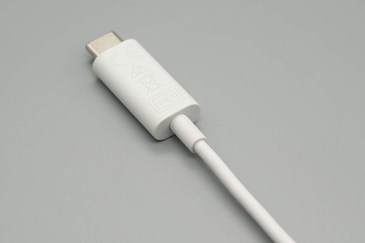
Both ends of the cable feature an anti-bending reinforcement design.
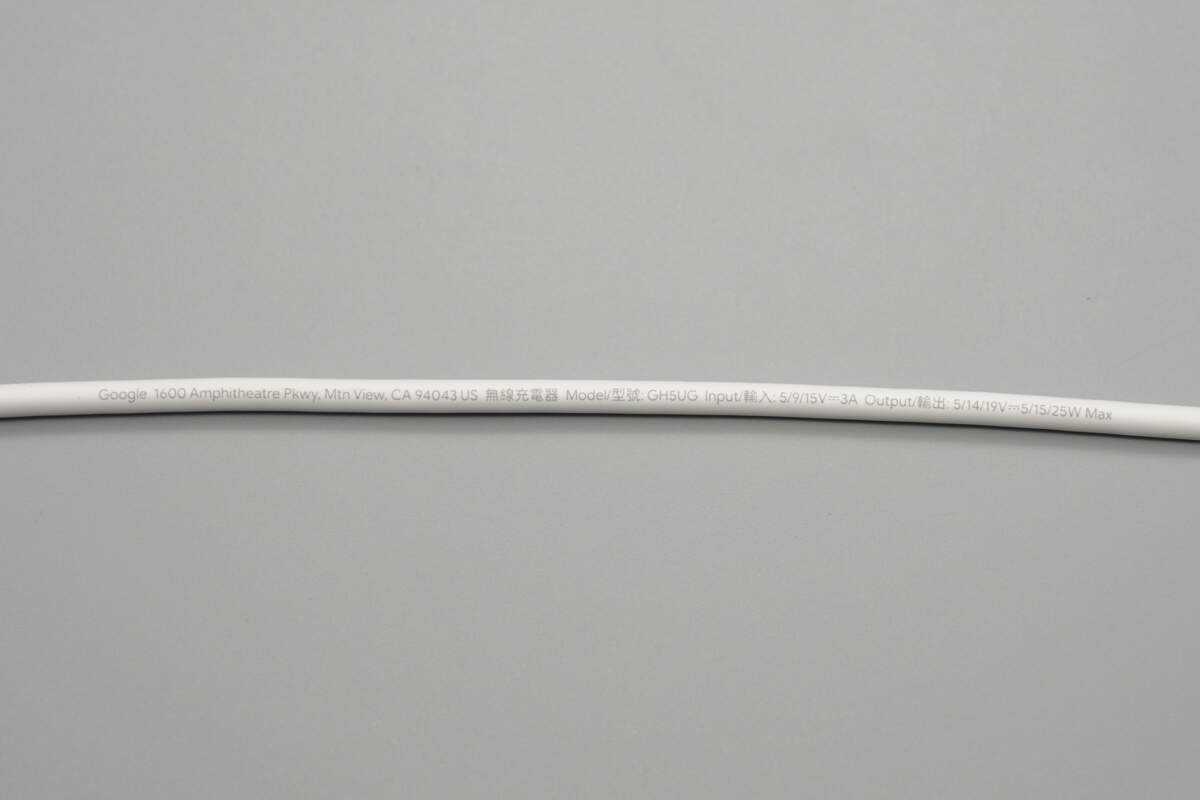
The cable is printed with the following specifications:
Model: GH5UG
Input: 5/9/15V⎓3A
Output: 5/14/19V⎓5/15/25W Max
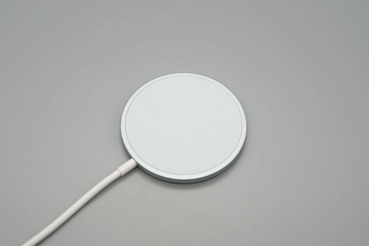
The wireless charging panel has a circular design, with the top cover made of a skin-friendly material.
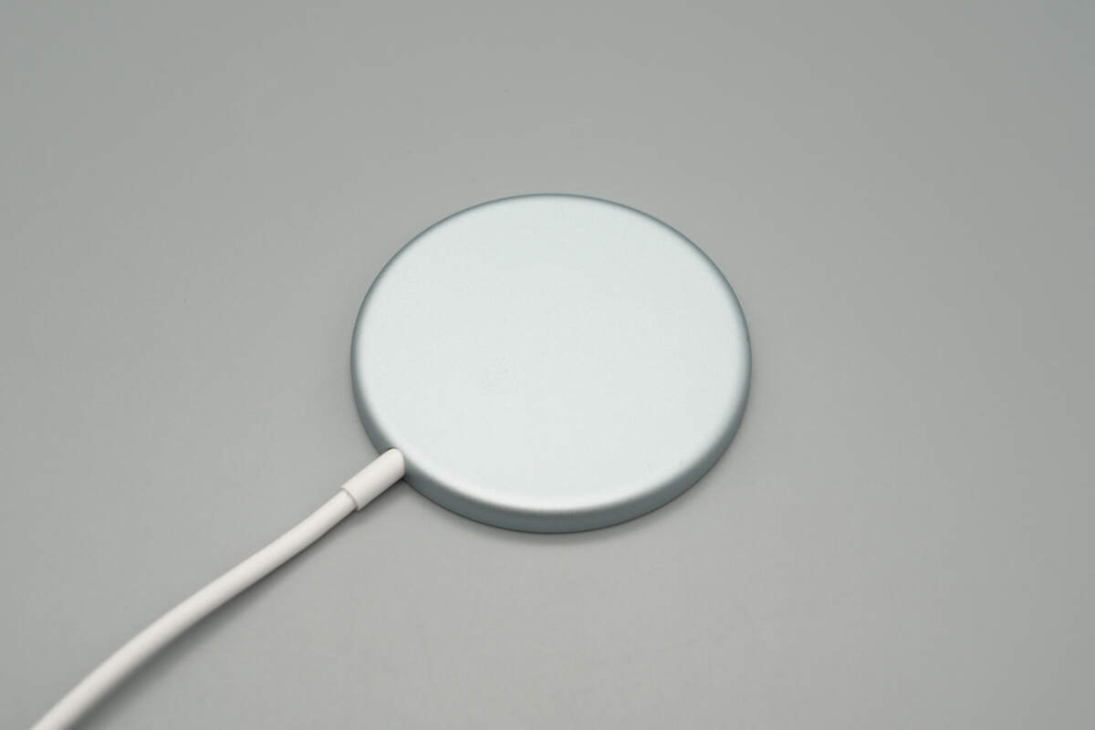
The bottom and sides feature a unibody metal casing with smoothly rounded edges.
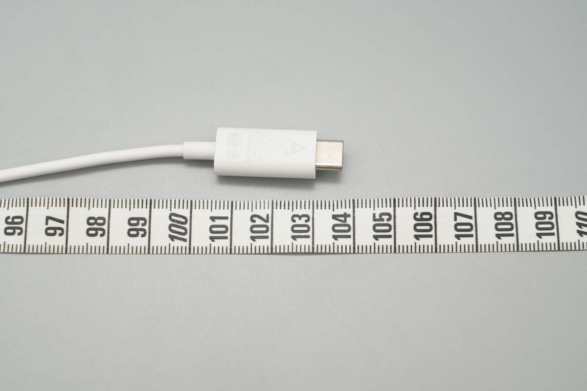
The length of the is about 104 cm (40.94 inches).
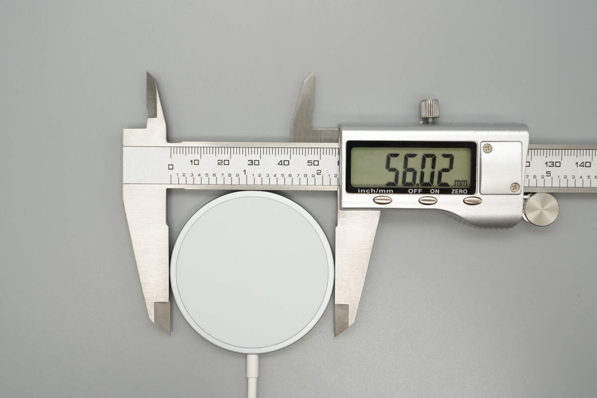
The diameter of the wireless charge panel is about 56.02 mm (2.21 inches).
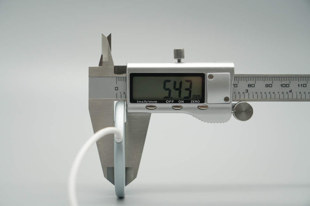
The thickness is about 5.43 mm (0.21 inches).
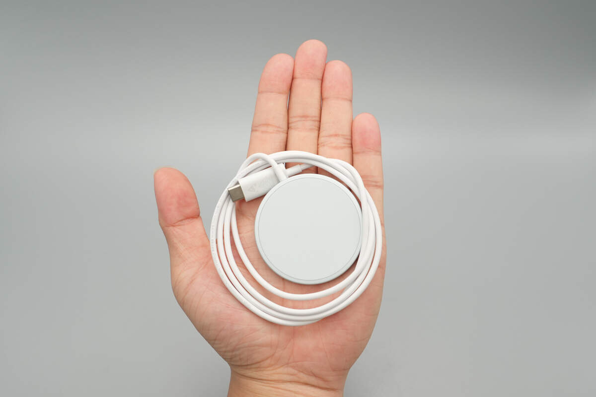
That's how big it is in the hand.
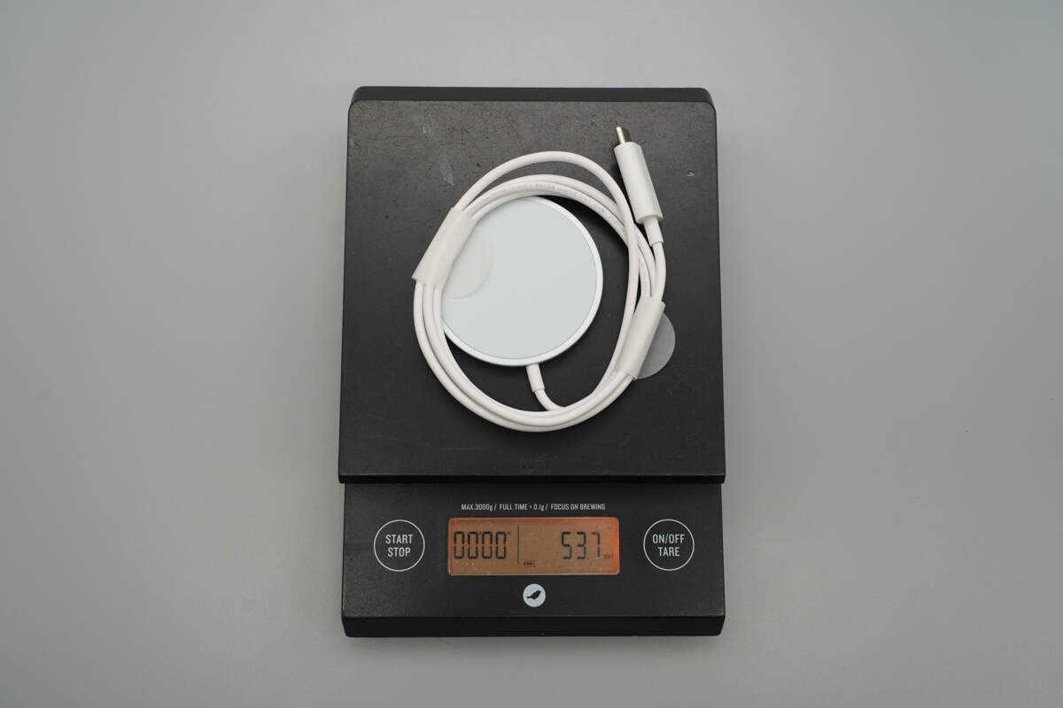
The weight is about 54 g (1.9 oz).
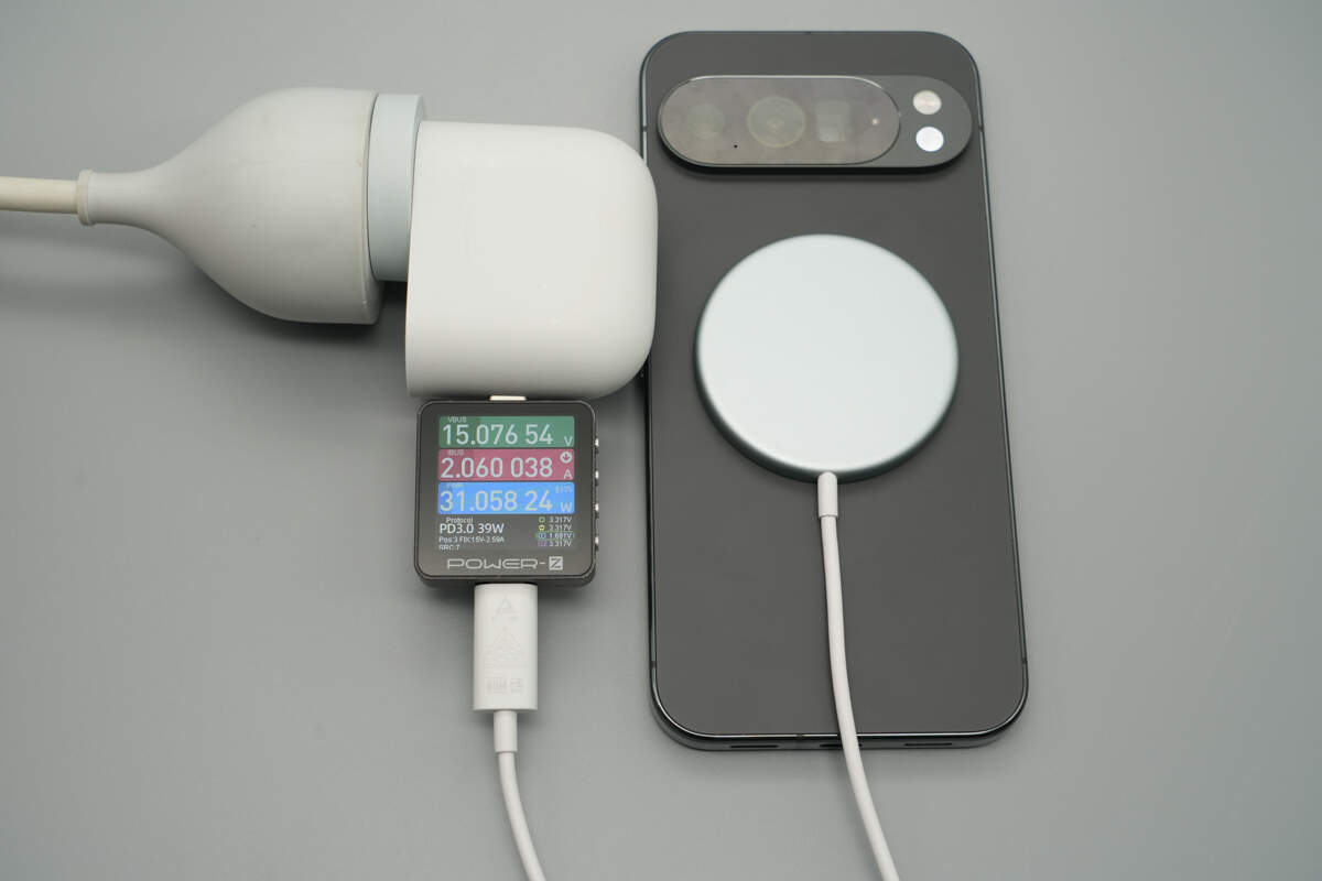
Using a Google 67W charger paired with it to charge the Google Pixel 10 Pro XL, the input power is about 31.06W.
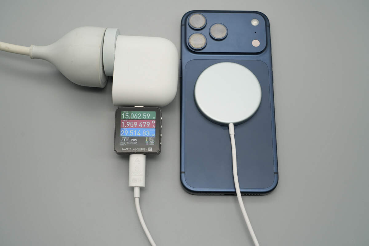
When charging the iPhone 17 Pro Max, the input power is about 29.51W.
Teardown
Next, let's start to take it apart and take a look at the internal components.
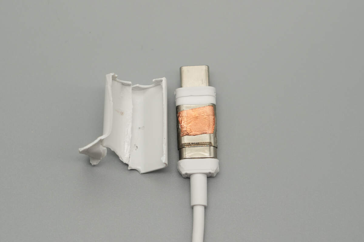
Cut open the USB-C connector housing. Inside, it features a steel sleeve reinforcement and is lined with copper foil.
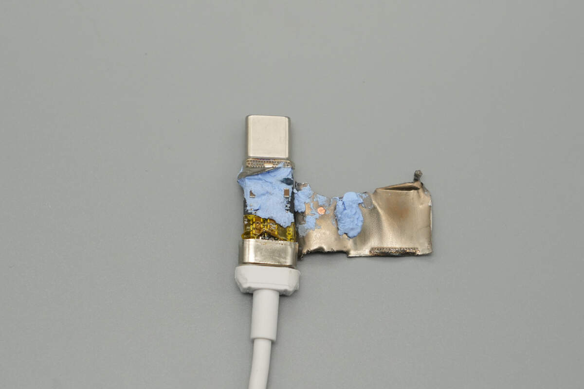
Remove the metal steel sleeve. The interior is filled with blue thermal gel, and the end of the PCB is wrapped with yellow insulating tape.
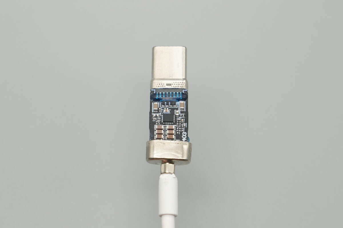
Clean the PCB. The adhesive is applied to the solder joints between the USB-C pins and the PCB to enhance the strength and durability.
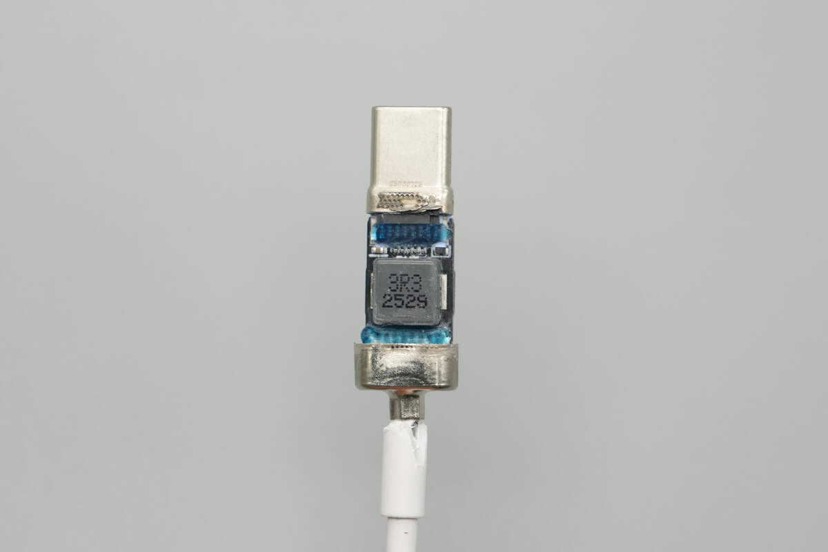
On the back, there is an inductor with adhesive applied to both ends for added protection.
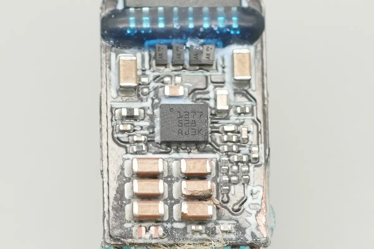
The synchronous boost converter is from TI, marked with "1377", and the model number is TPS61377. This is a high-voltage synchronous boost converter featuring a 50mΩ low-side power switch and a 40mΩ high-side rectifier switch, providing an efficient and compact solution.
It has a wide input voltage range of 2.9-23V, with an output voltage of up to 25V and a 6A switching current capability. The device comes in a small 2.5mm × 2.0mm HotRod™ Lite VQFN package, offering an extremely compact solution size.
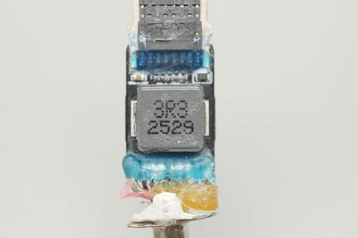
A close-up of the 3.3μH inductor.
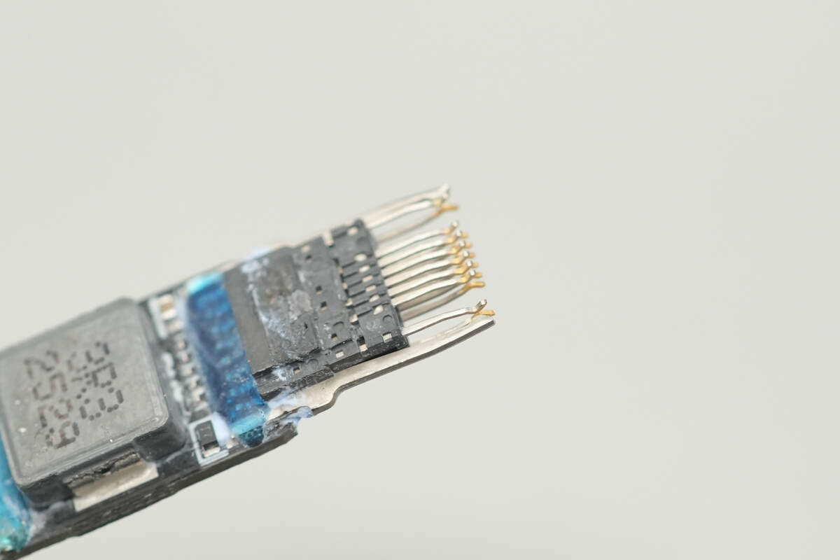
Remove the metal casing of the USB-C connector. The front ends of the pins are gold-plated.
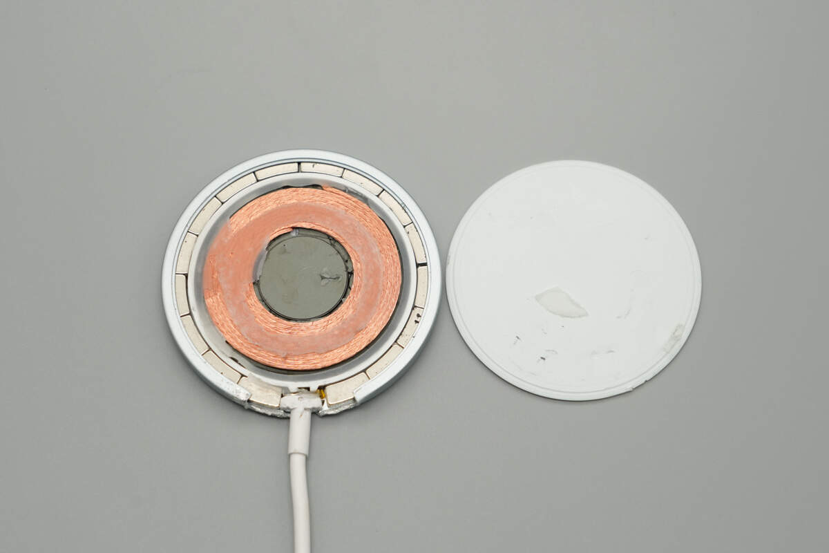
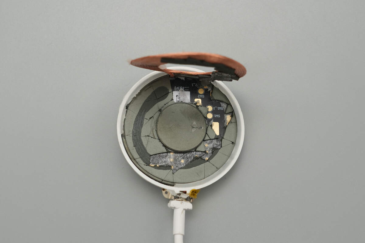
Remove the top cover of the wireless charging panel.
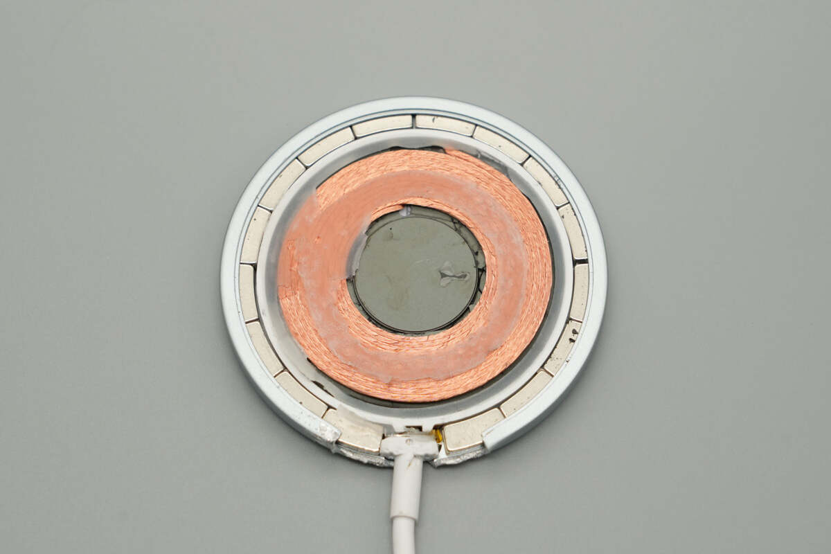
The wireless charging coil is secured with adhesive, and the edges feature a magnetic ring composed of 16 magnets.
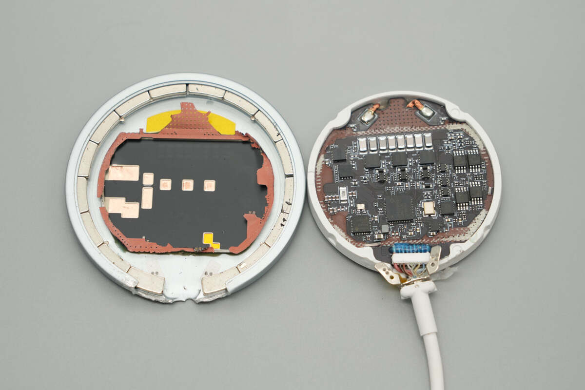
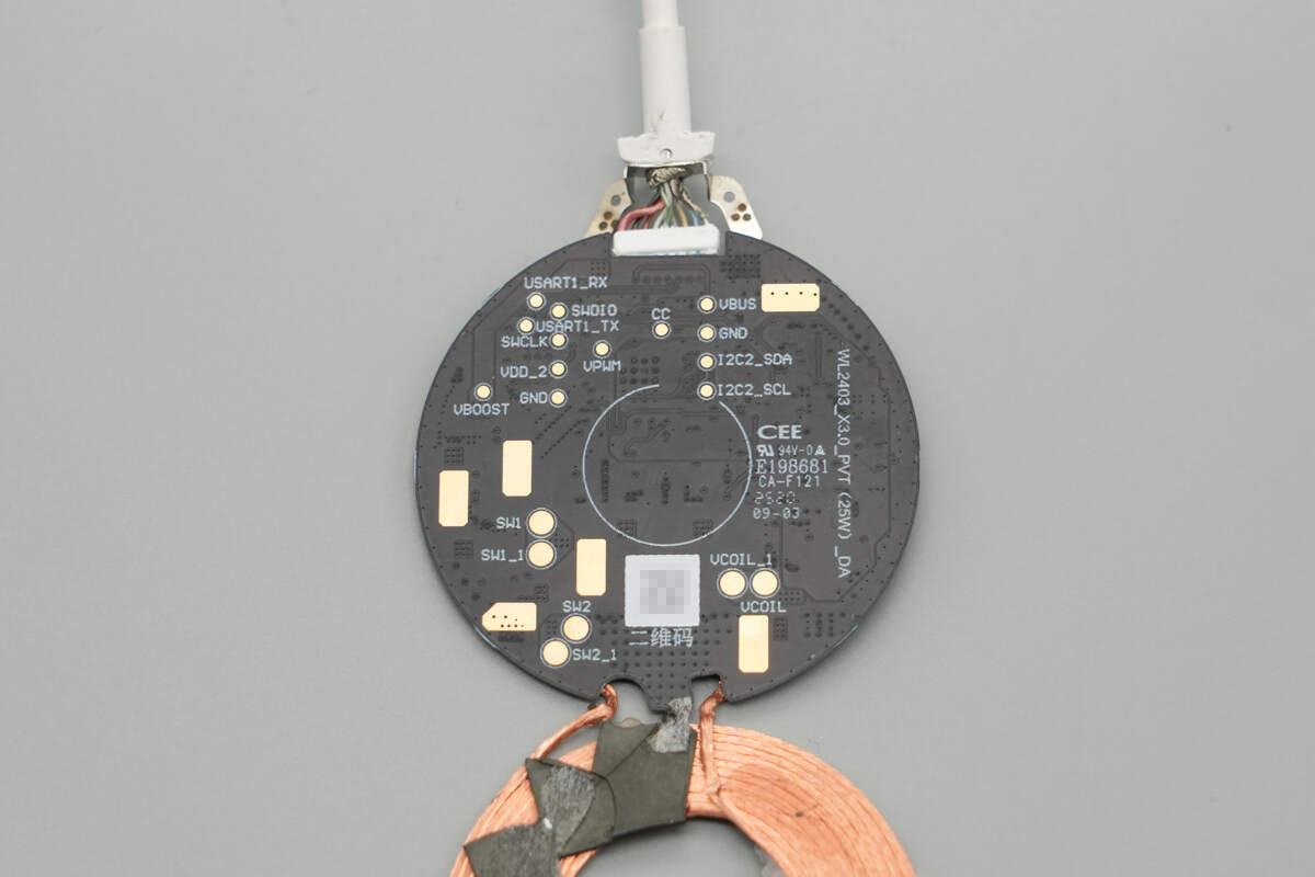
Remove the PCBA module. The bottom area corresponding to the PCB is covered with a shielding cover, which is fixed with adhesive to the metal casing. Both sides of the shielding cover are lined with copper foils and insulating stickers.
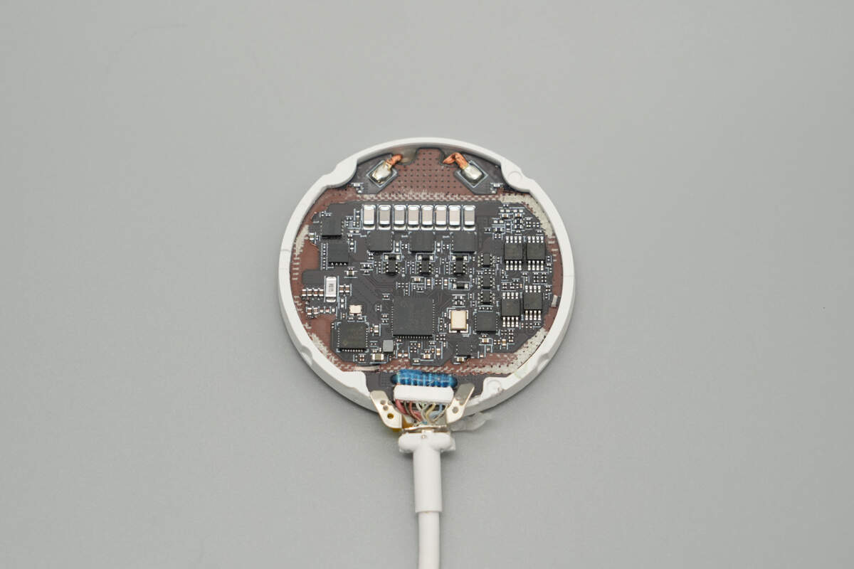
The edge of the PCB is fitted with a plastic ring.
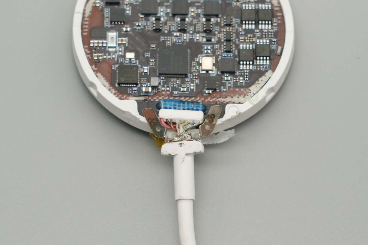
The connection between the cable and the panel is secured with a metal piece, and the wire core solder joints are reinforced with adhesive.
A magnetic isolation sheet is placed between the coil and the PCB.
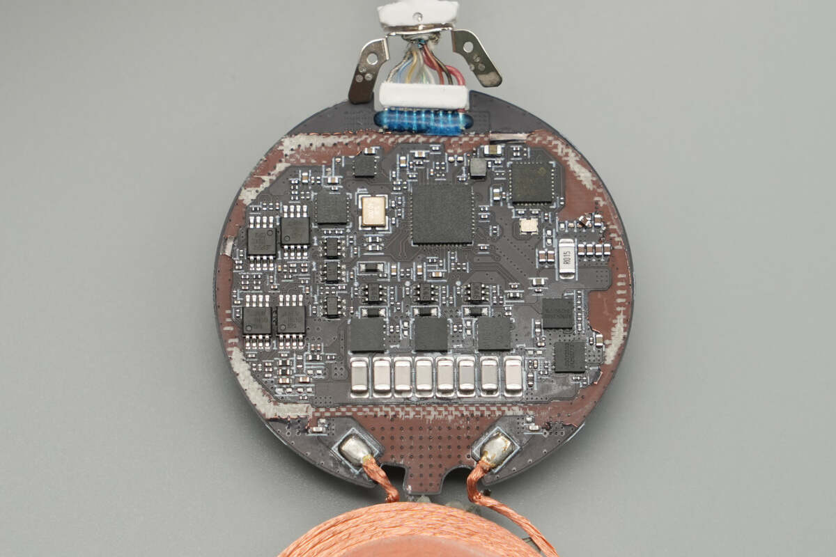
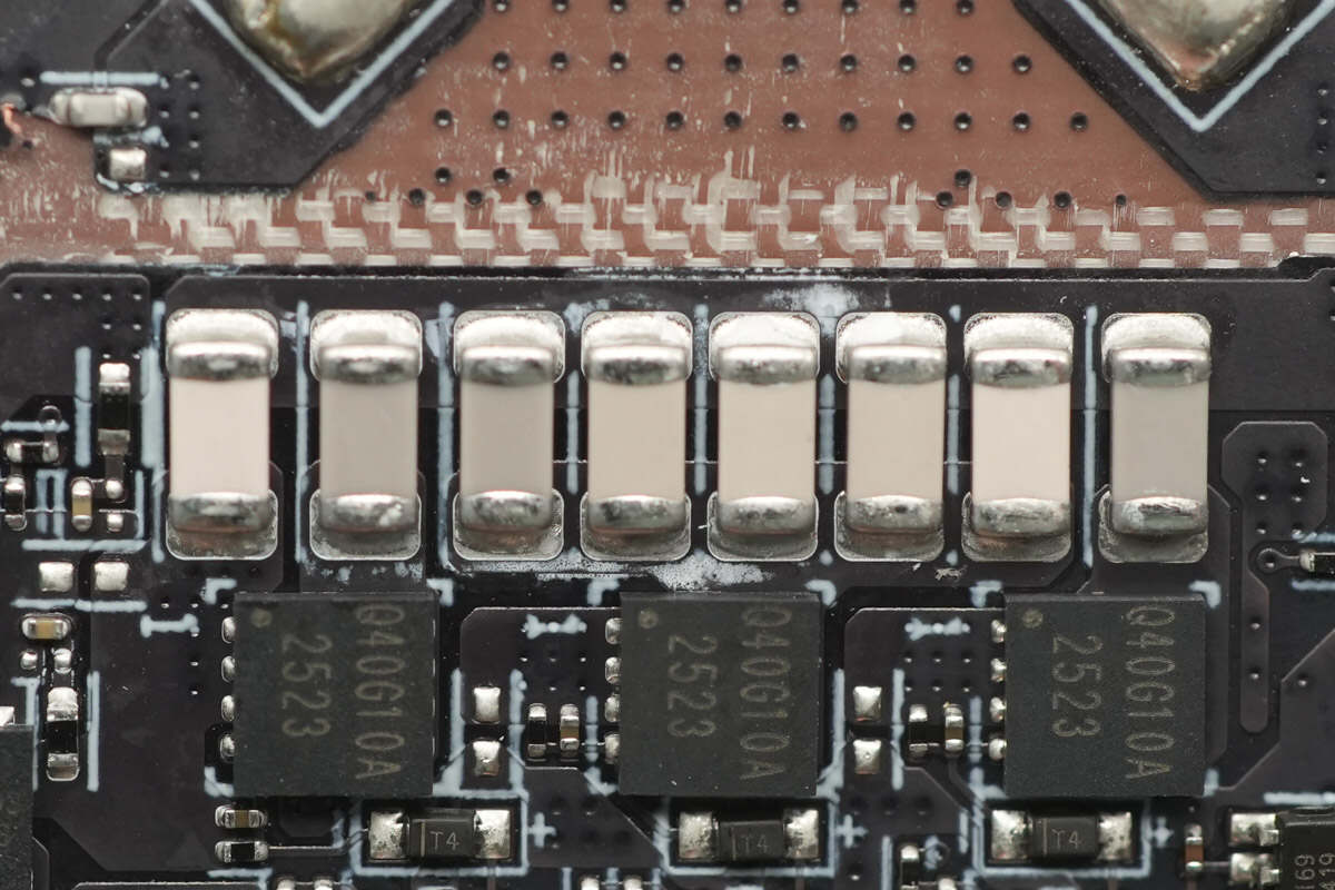
The front of the PCB features components such as a linear voltage regulator, MCU, wireless charging master control chip, security chip, dual op-amps, wireless charging power MOSFETs, resonant capacitors, and switching MOSFETs.
The back of the PCB has no components, and several areas show exposed copper.
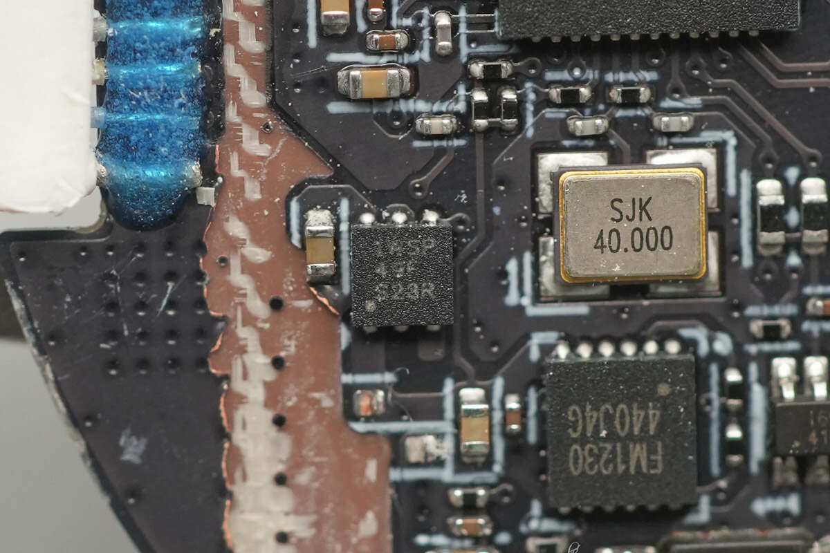
The linear voltage regulator is also from Texas Instruments, marked with "1WSP" and the model number TPS7A25. This is a low-dropout (LDO) linear regulator, combining a 2.4-18V input voltage range with extremely low quiescent current (IQ) characteristics.
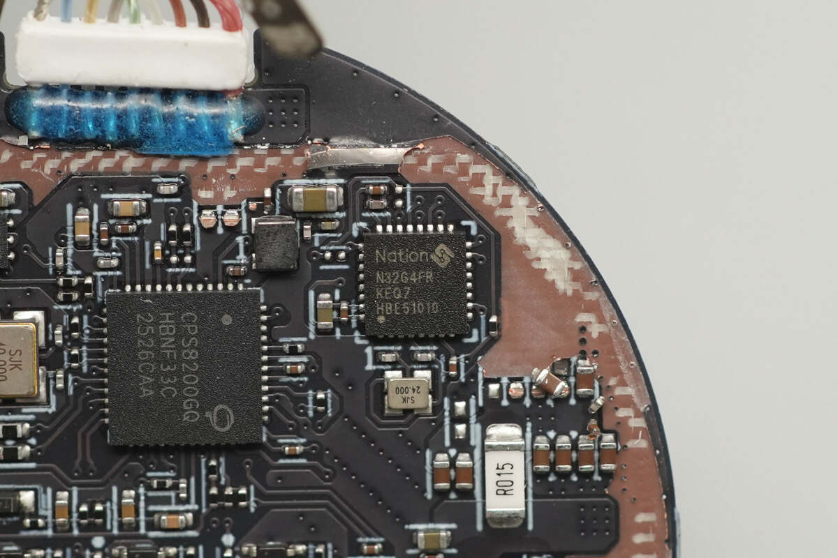
The MCU used for overall system control is from Nations, model N32G4FRKEQ7. This series of MCUs features a 32-bit ARM Cortex-M4F core with a maximum operating frequency of 144MHz, supporting floating-point operations and DSP instructions. It integrates up to 512KB of Flash for secure storage of fingerprint data, 144KB of SRAM, and includes two 12-bit 4.7Msps ADCs, two 1Msps 12-bit DACs.
The MCU also integrates multiple communication interfaces, including U(S)ART, I2C, SPI, QSPI, USB, CAN, and one SDIO interface. It supports a digital camera (DVP) interface and is compatible with mainstream semiconductor and optical fingerprint sensors. Additionally, it includes a hardware acceleration engine for cryptographic algorithms.
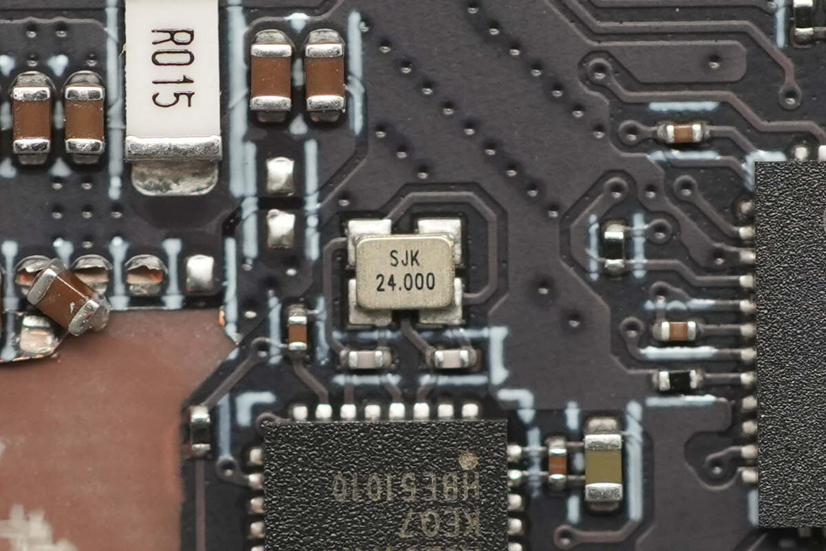
A close-up of the 24.000MHz passive clock crystal oscillator.
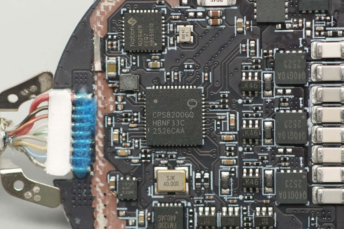
The wireless charging master control chip is from CPS, model CPS8200. It is a highly integrated wireless charging transmitter chip that features an internal 32-bit processor. The chip integrates 64+2KB MTP, 32KB ROM, and 2KB SRAM, with the MTP supporting read-write protection and programmability via CC and DPDN. It includes two I2C interfaces and two UART interfaces. The chip also integrates a switching buck converter, linear voltage regulator, DC-DC controller, full-bridge driver, communication module, and multi-channel 12-bit ADC.
The CPS8200 supports QC2.0/QC3.0/PD3.1/SCP/AFC fast charging protocols and integrates three pairs of half-bridge drivers, capable of either boost or buck conversion. It supports fixed-frequency voltage regulation charging, and when paired with the appropriate MOSFETs, it can form a complete Qi2 wireless charger. It supports a 24V input supply voltage, with the power stage supporting up to 45V. The chip also includes over-voltage, over-current, and over-temperature protection features.
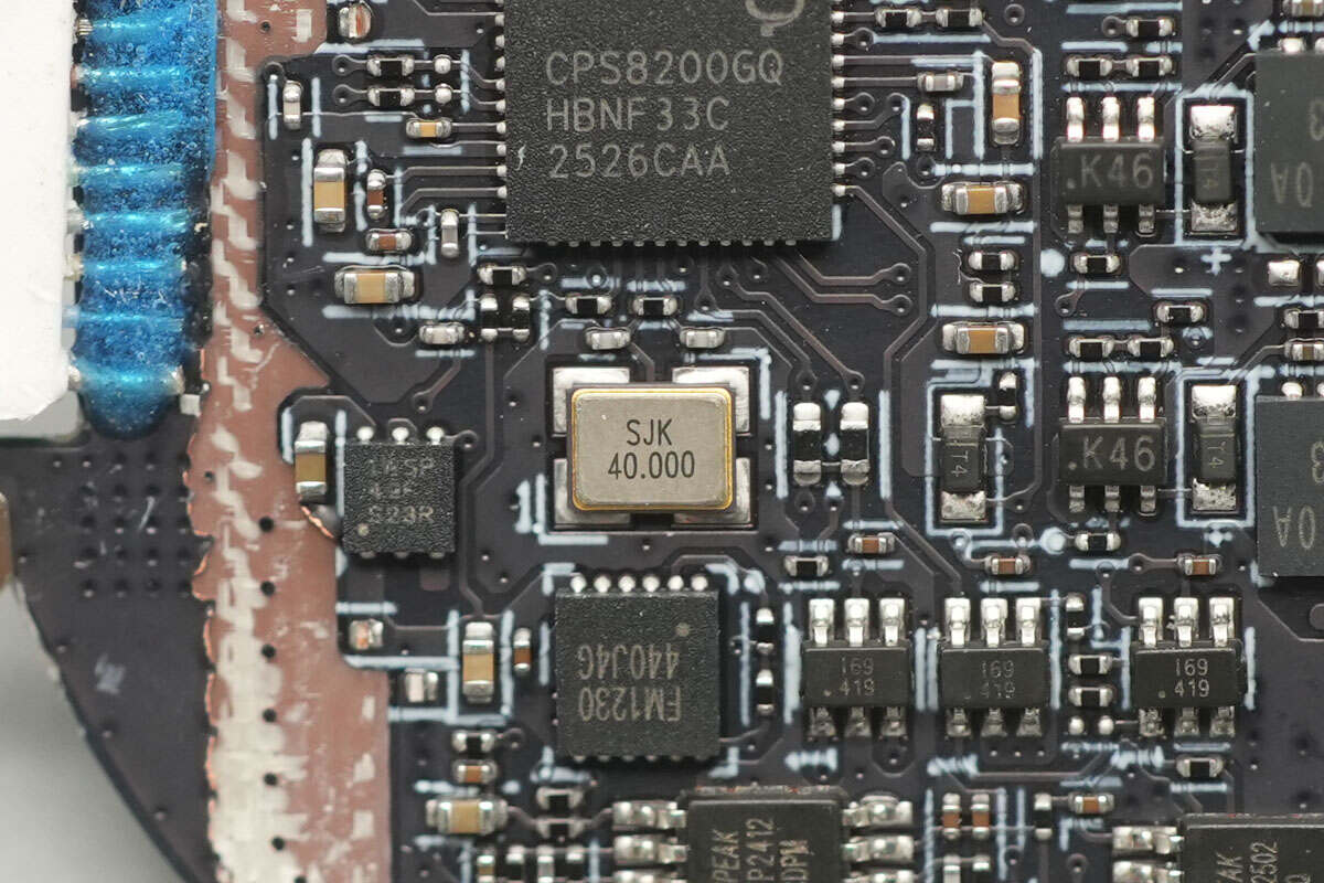
A close-up of the 40.000MHz passive clock crystal oscillator.
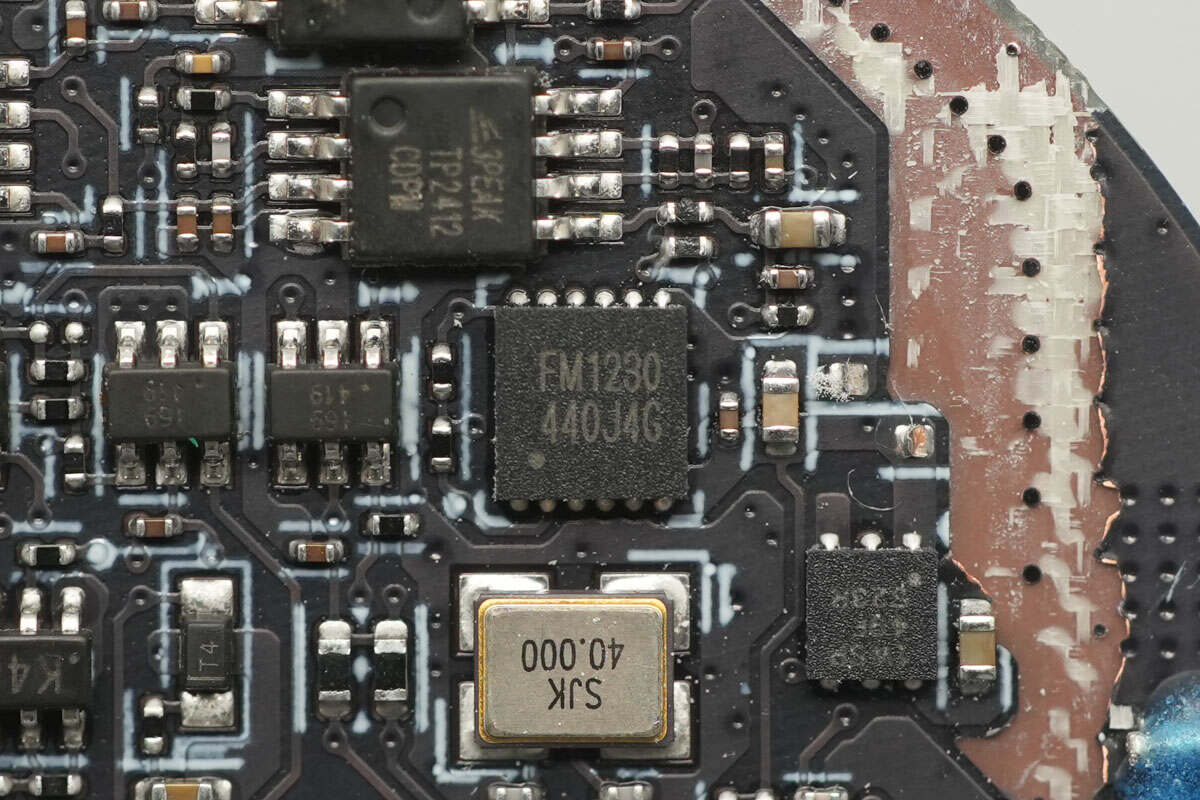
The security chip is from FUDAN, model FM1230. It supports symmetric algorithms such as DES/TDES, AES, and SM4, as well as asymmetric algorithms including RSA, ECC, and SM2, along with hash algorithms like SHA1, SHA224, SHA256, and SM3.
The FM1230 offers various security features, including support for symmetric and asymmetric encryption/decryption operations, secure storage, and identity authentication. It can be used in applications such as contact-based ESAM/PSAM modules and SE (Secure Element) security modules.
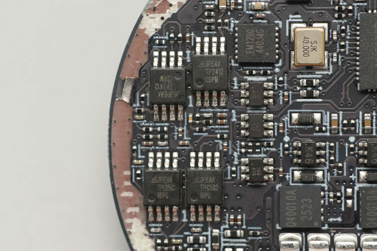
The four Dual Op Amps are from 3PEAK, with two pairs of models: TP2412 and TPH2502. The TP2412 is a low-noise dual op-amp that supports rail-to-rail input and output. The TPH250x series comprises single, dual, or quad-channel low-power, high-speed, unity-gain stable, rail-to-rail input/output operational amplifiers. The TPH2502 is the dual-channel version and is available in both SOP8 and MSOP8 packages.
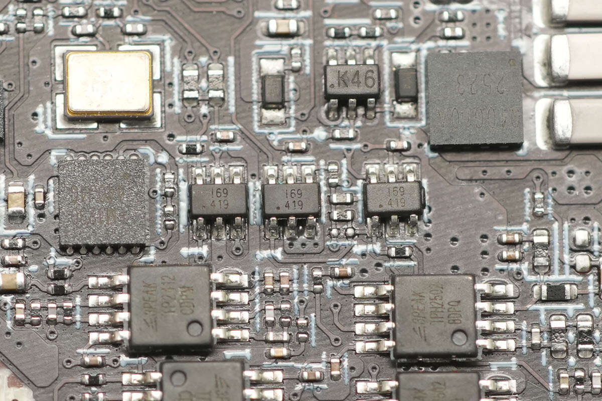
The three analog switches are from Belling, marked with I69, and the model is BL1551B. This is a single-channel broadband, fast single-pole double-throw (SPDT) analog switch, with a typical on-resistance of 2.7Ω (when VCC = 5.0V) and a wide supply voltage range of 1.8-5.5V.
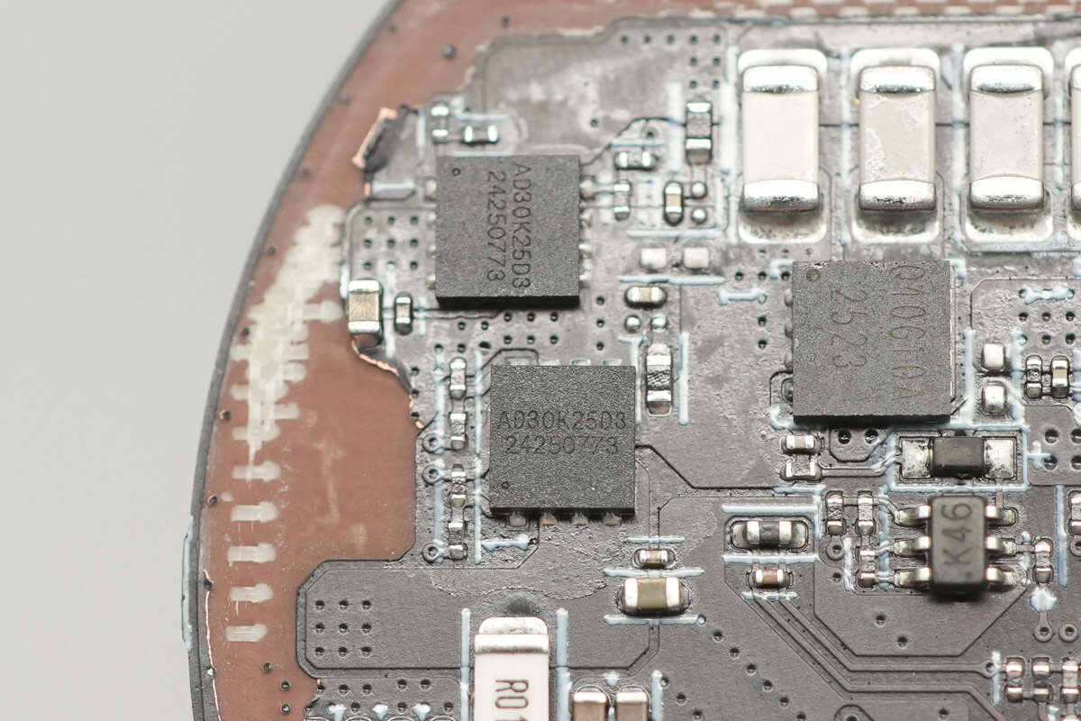
The wireless charging power MOSFETs are from ADAMANT, model AD30K25D3. These are dual NMOS transistors with a voltage rating of 30V, and they come in a DFN3030 package.
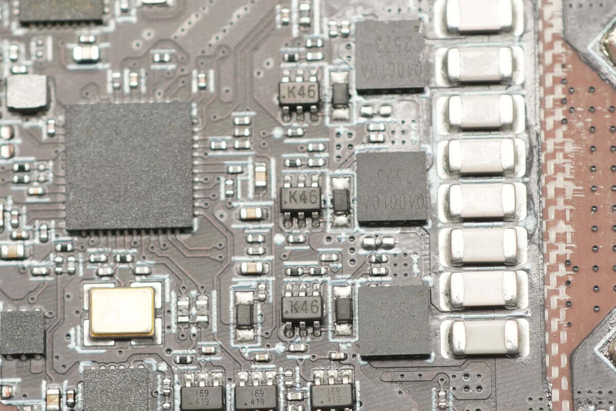
The three marked with K46 are dual transistors.
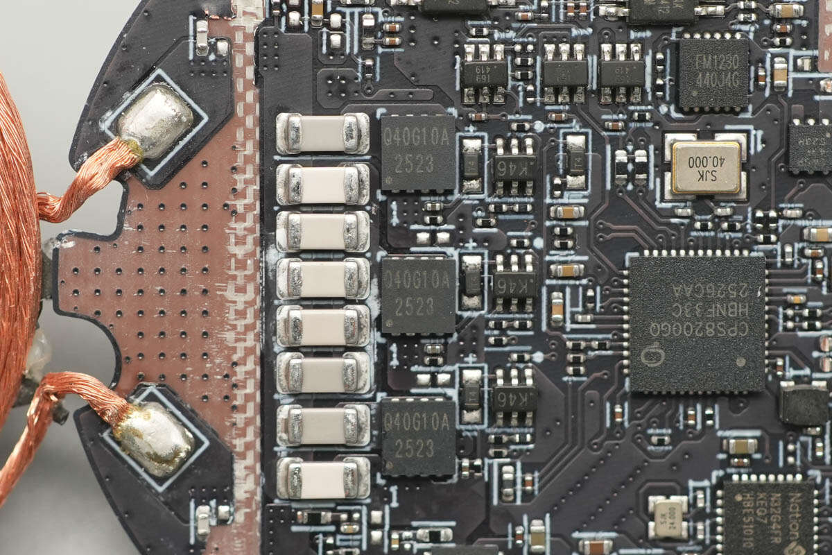
The MOSFETs used for resonant capacitor switching are from YJ, model YJQ40G10A. These are NMOS transistors with a voltage rating of 100V, a drain-source on-resistance of 18.5mΩ, and are packaged in a DFN3333-8L form factor.
A close-up of the NPO resonant capacitors.
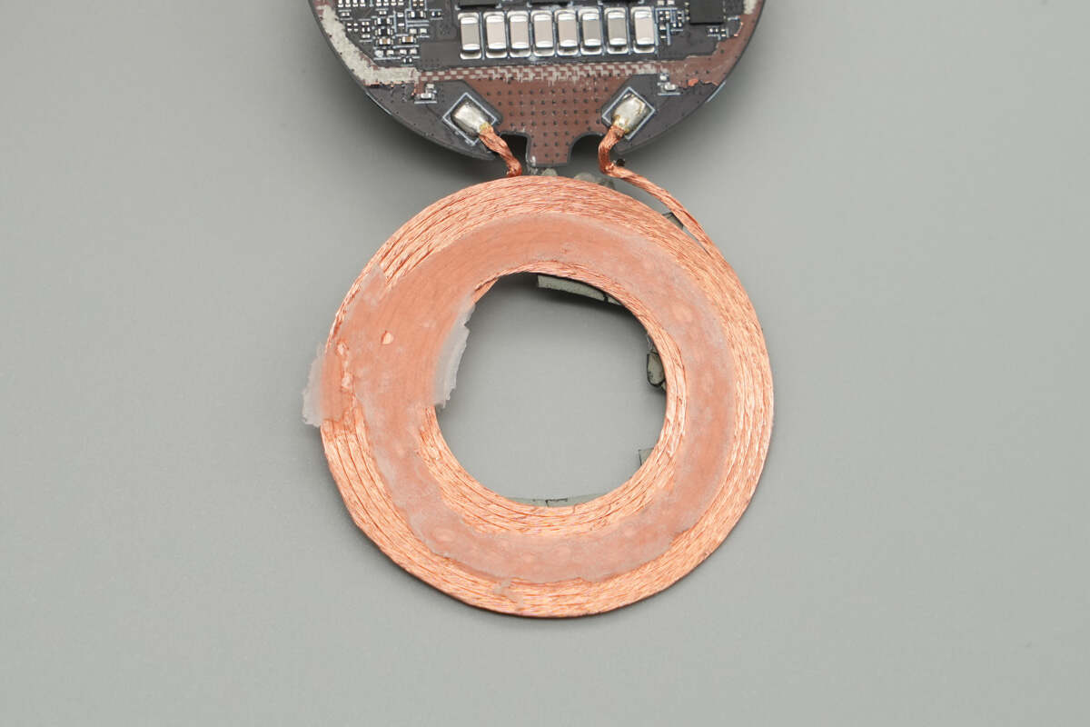
The coil is wound using Litz wire.
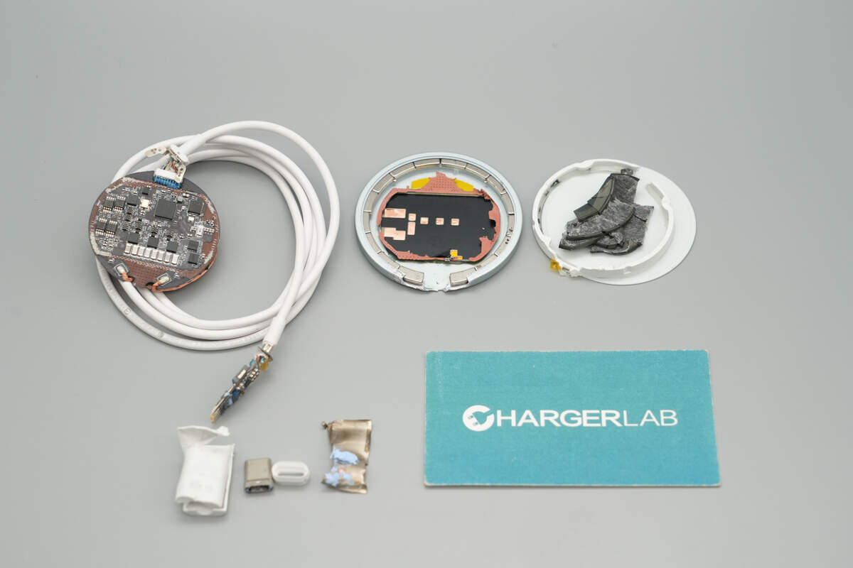
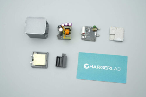
Well, those are all components of the Google 25W Qi2.2 Magnetic Wireless Charger.
Summary of ChargerLAB
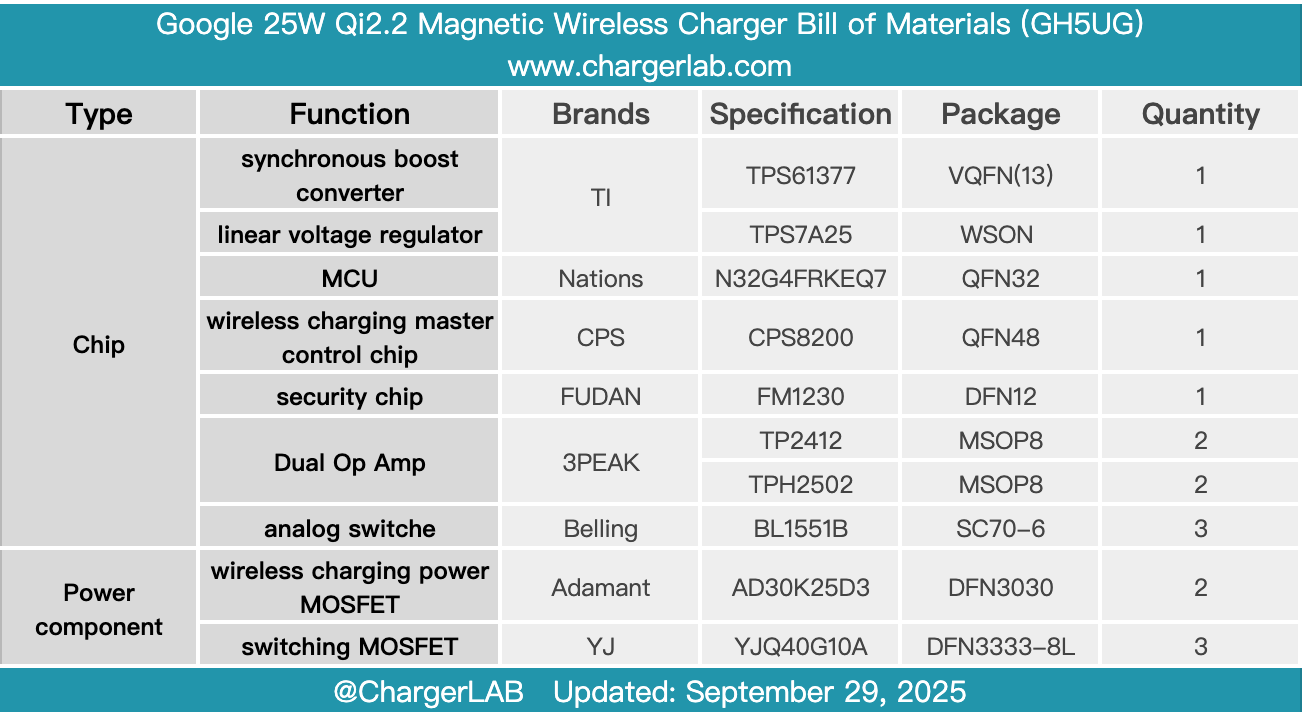
Here is the component list of the Google 25W Qi2.2 Magnetic Wireless Charger for your convenience.
It comes with a built-in USB-C cable, and the front of the wireless charging panel features a skin-like texture. The sides and back are made from a unibody metal casing, offering high drop resistance and effective heat dissipation. It supports the latest Qi 2.2 wireless charging standard and provides 25W fast wireless charging, meeting the charging needs of devices like the Google Pixel 10 Pro XL. It is also well-suited for the Apple iPhone 17 series and Xiaomi 17 series, among other models.
After taking it apart, we found that the boost circuit is integrated within the USB-C connector, utilizing Texas Instruments' ultra-compact synchronous boost solution, the TPS61377. Inside the wireless charging panel, the system is powered by the Nations N32G4FRKEQ7 MCU and the CPS8200 wireless charging master control chip. The security chip is the FUDAN FM1230.
The front of the PCB is covered with a shielding cover, while the wireless charging coil is reinforced with adhesive to enhance anti-interference performance and ensure stability. The build quality is impressive, reflecting careful design and attention to detail.
Related Articles:
1. Teardown of Apple 25W Qi2.2 + MagSafe Charger A3502 (HK Version)
2. Teardown of EcoFlow RAPID 170W 25000mAh Power Bank (EF-HB-002)
3. Teardown of MEAN WELL 1500W Switching Power Supply (SE-1500-24)