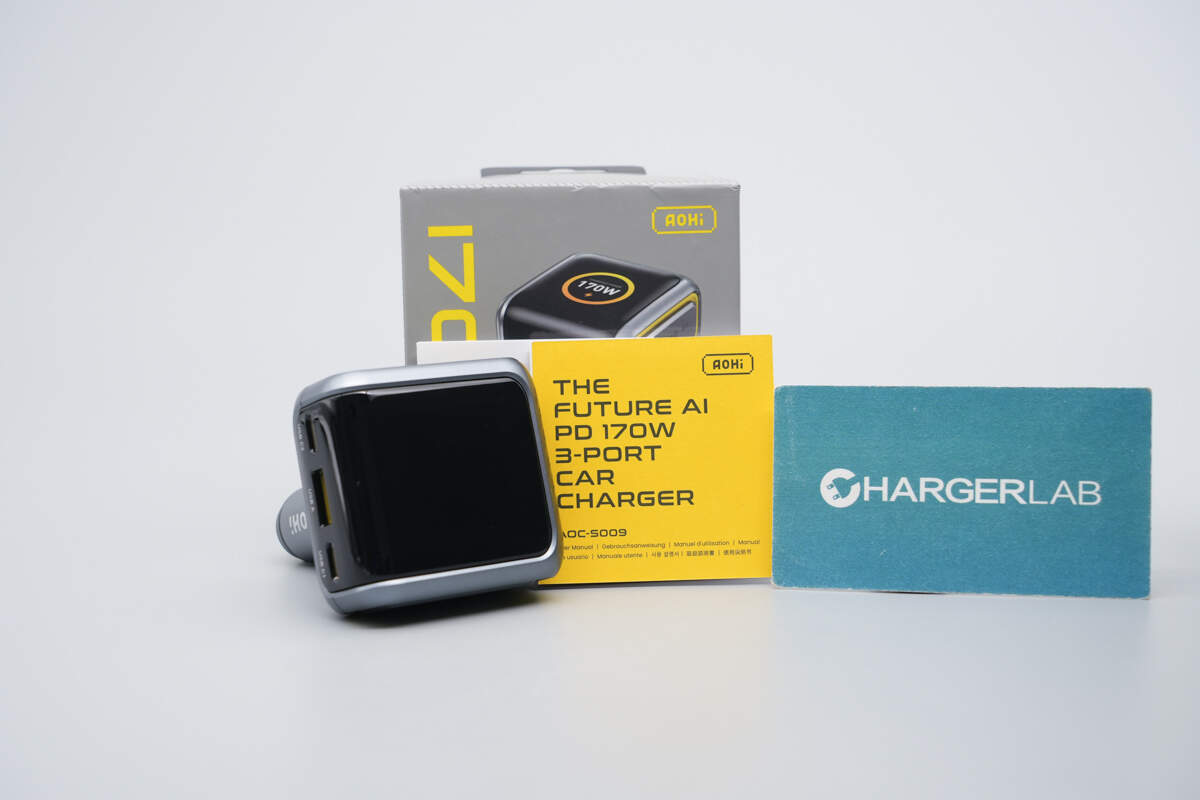
Introduction
AOHi has launched a 170W intelligent AI animated display car charger. The charger is equipped with an LCD screen that provides real-time readouts of output power and operating temperature. It features two USB-C ports and one USB-A port. The USB-C ports support up to 140W PD 3.1 fast charging, are compatible with 100W PPS and 63W UFCS protocols, and enable automatic power distribution of up to 100W + 70W to meet the needs of charging multiple devices simultaneously.
The AI holographic animated display supports five interactive modes, including super fast-charging animation, total output power display, real-time temperature monitoring, multi-port power distribution status, and charging status animations. Next, we will take a closer look at the design of this product.
Product Appearance
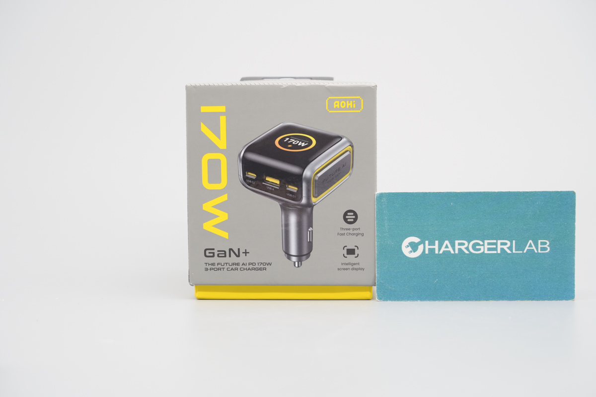
The top-right corner of the packaging box features the AOHi logo, while the center displays the product's appearance along with its key selling points.
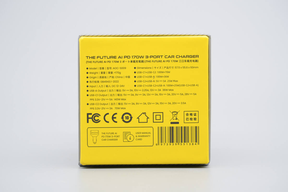
Detailed specifications are printed on the bottom of the packaging.
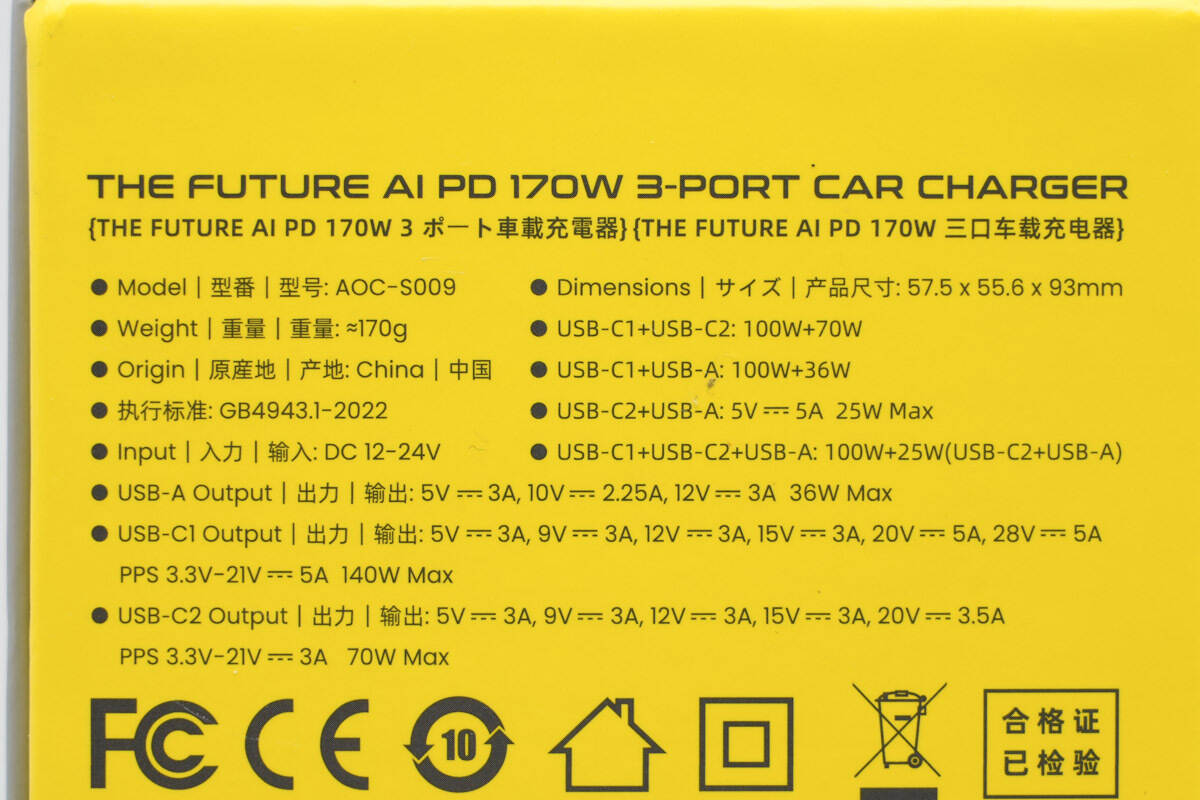
Model: AOC-S009
Product weight: 170g
Dimensions: 57.5 × 55.6 × 93 mm
Compliance standard: GB 4943.1-2022
Input: DC 12–24V
USB-C1 output: 5V⎓3A, 9V⎓3A, 12V⎓3A, 15V⎓3A, 20V⎓5A, 28V⎓5A
PPS: 3.3–21V⎓5A, 140W max
USB-C2 output: 5V⎓3A, 9V⎓3A, 12V⎓3A, 15V⎓3A, 20V⎓3.5A
PPS: 3.3–21V⎓3A, 70W max
USB-A output: 5V⎓3A, 10V⎓2.25A, 12V⎓3A, 36W max
USB-C1 + USB-C2: 100W + 70W
USB-C1 + USB-A: 100W + 36W
USB-C2 + USB-A: 5V⎓5A, 25W max
USB-C1 + USB-C2 + USB-A: 100W + 25W (USB-C2 + USB-A)
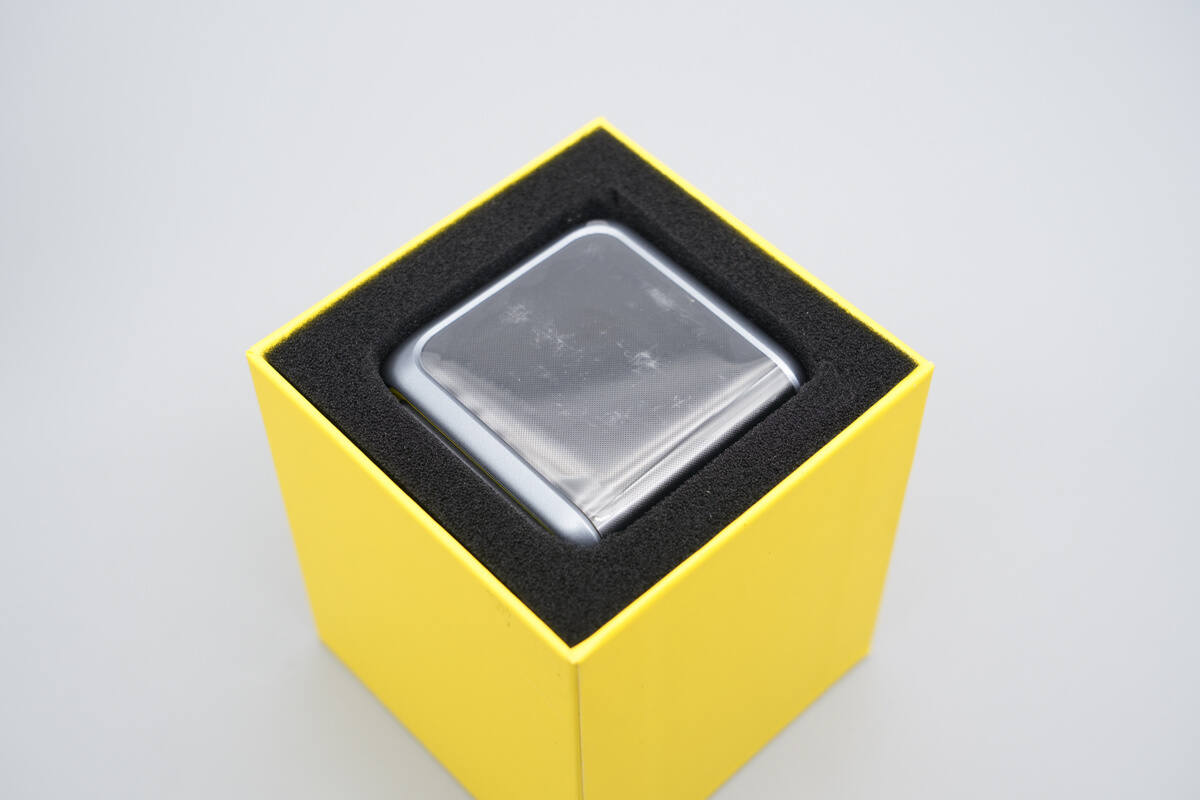
Foam padding is used inside the packaging to protect the charger.
The package includes the car charger and a user manual.
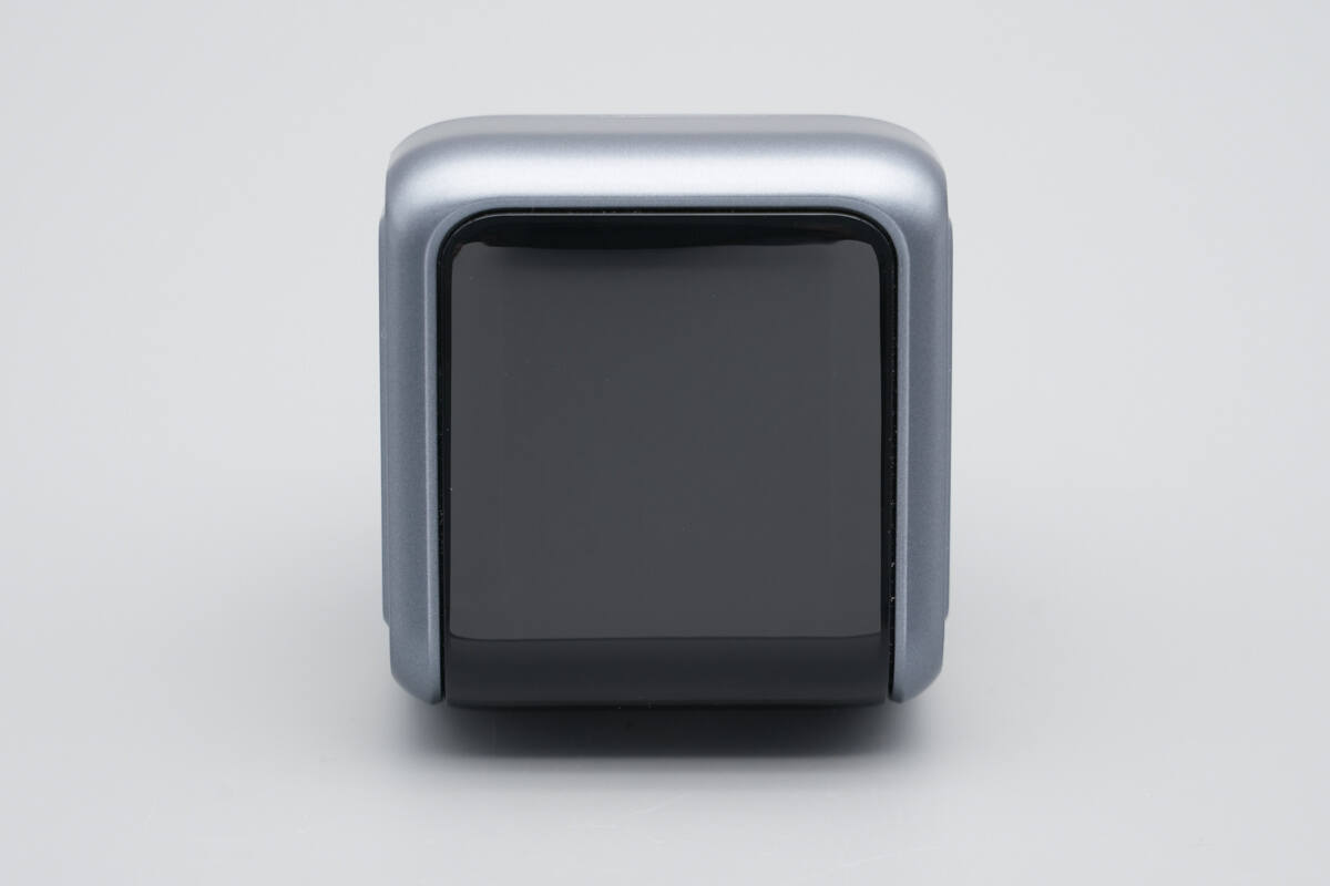
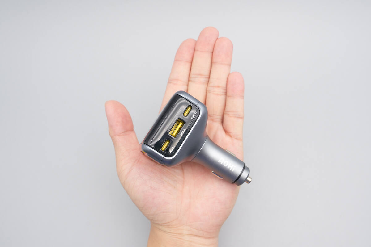
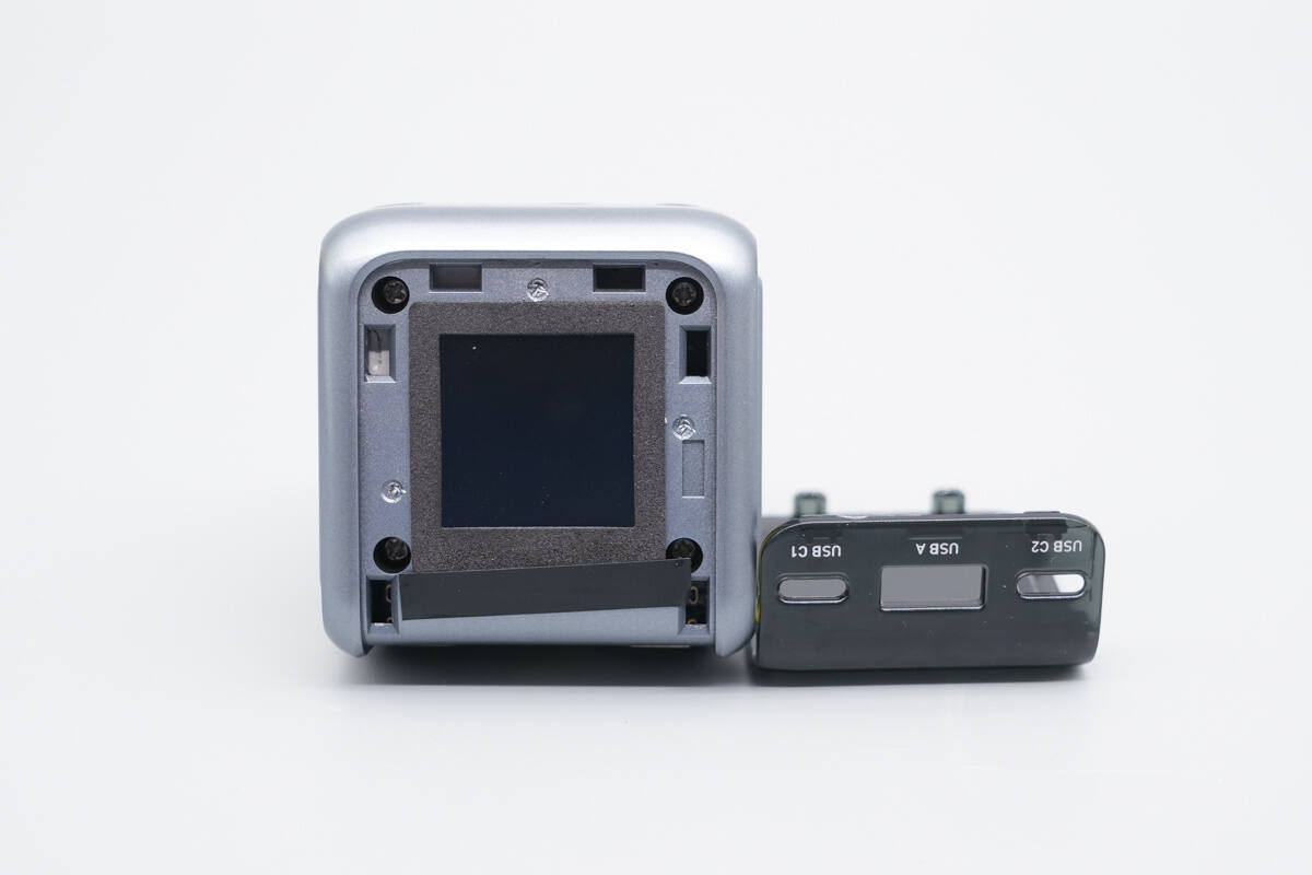
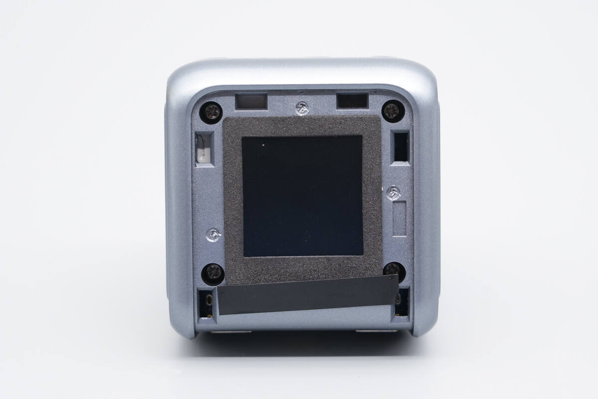
A concealed display is integrated into the top of the car charger.
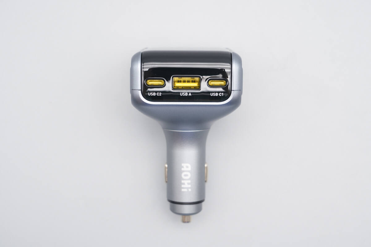
Below the front panel, there is one USB-C port and two USB-A ports.
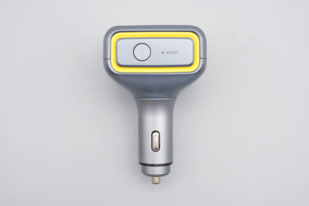
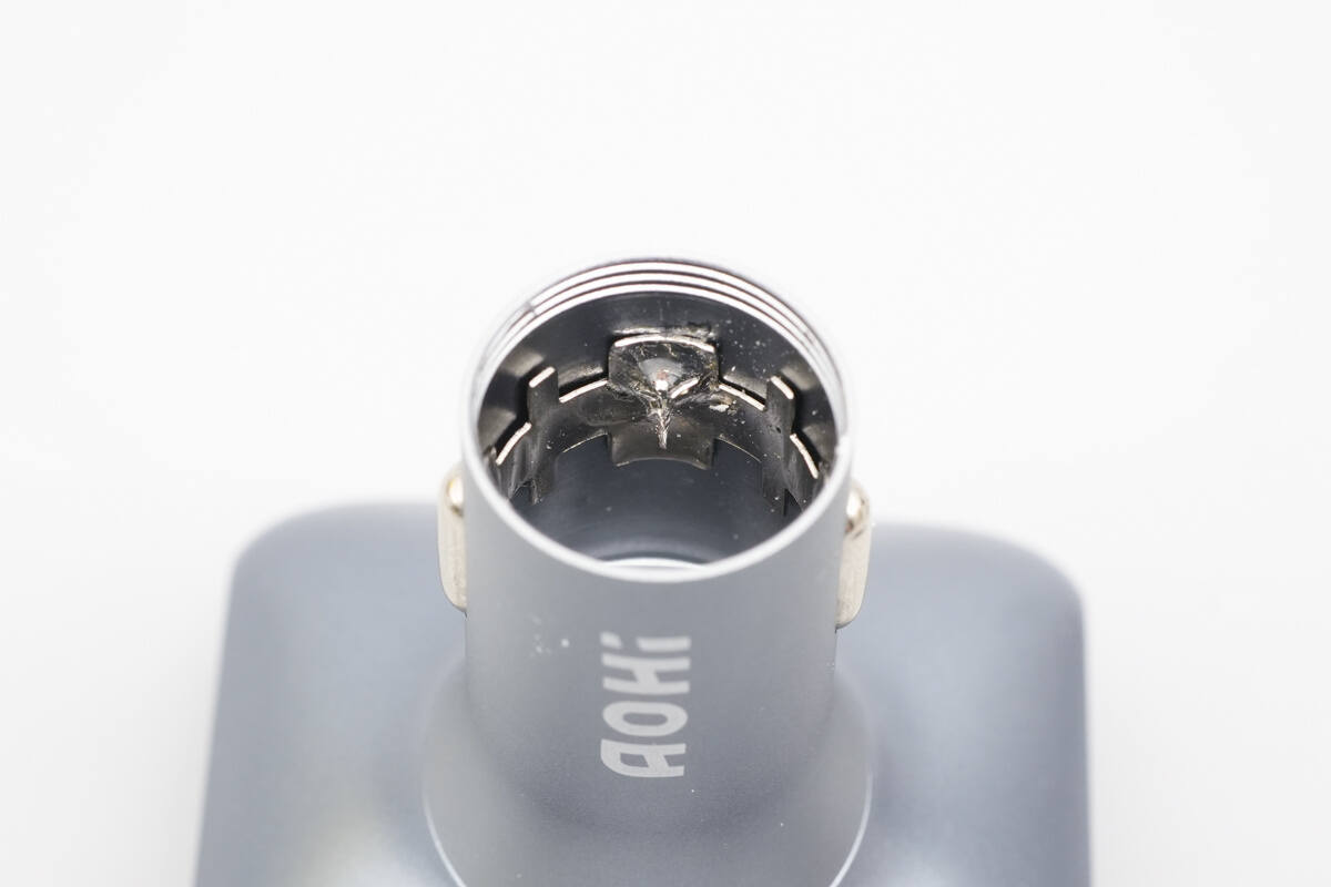
A function button is located on the side.
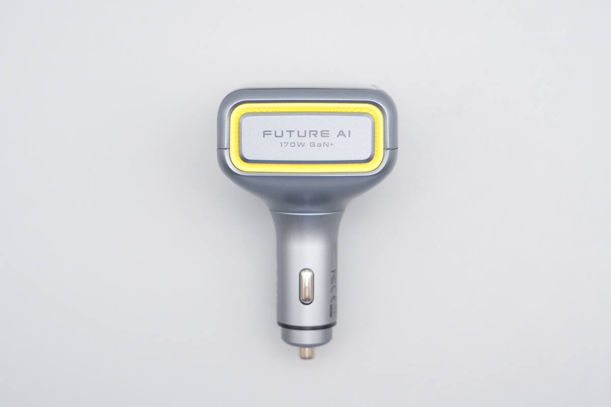
The opposite side is labeled with “FUTURE AI 170W GaN+”.

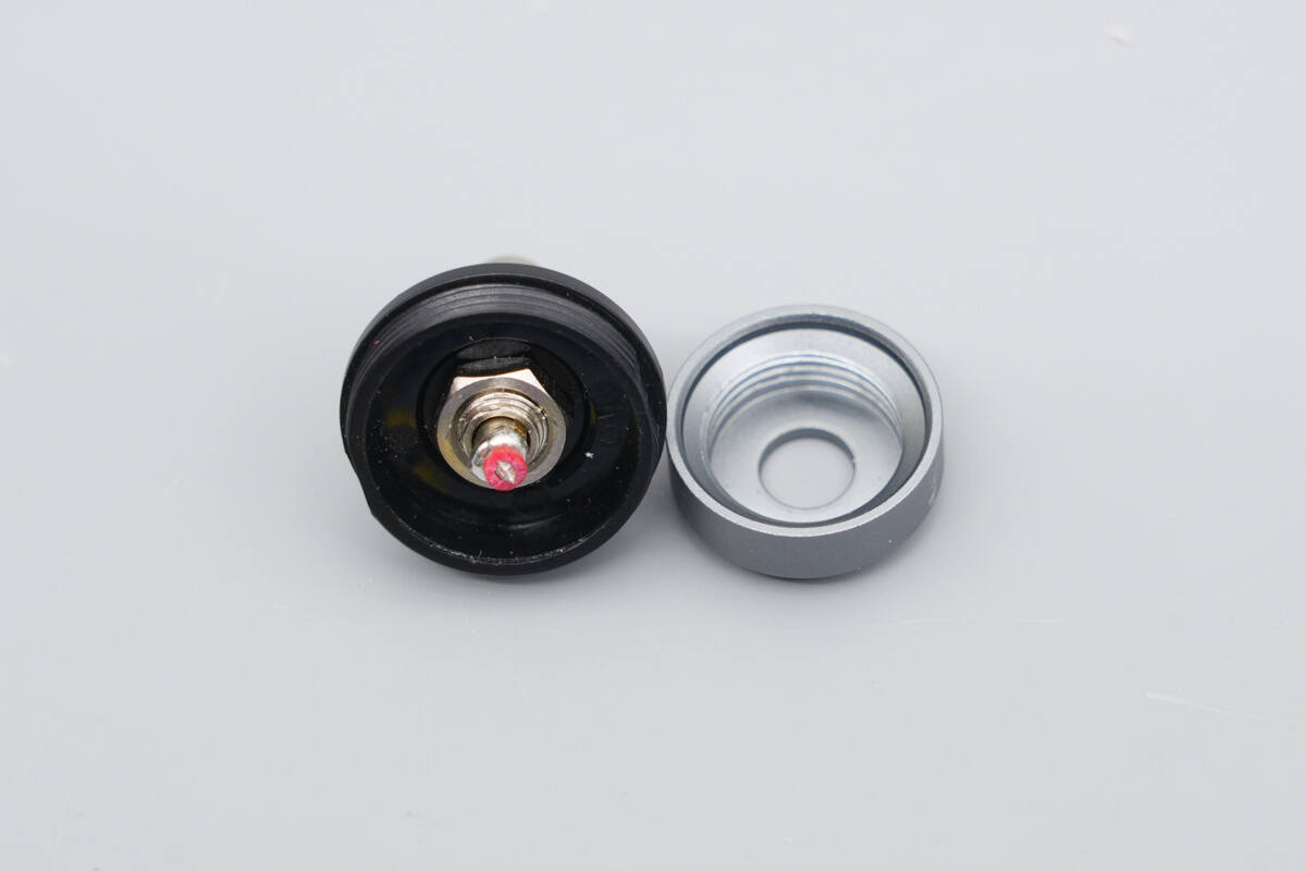
The front section of the car charger features an aluminum alloy housing with a plastic insulating ring positioned between the positive and negative terminals.
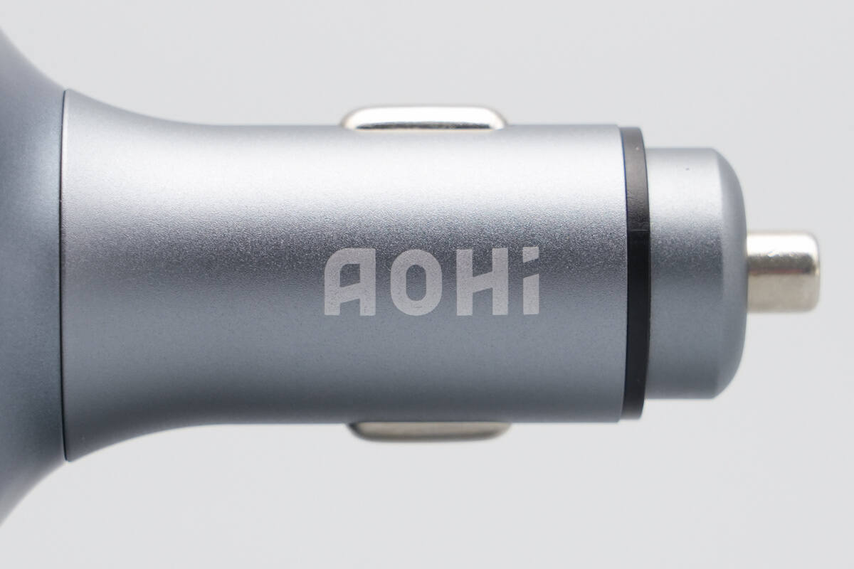
The AOHi branding is printed on it.
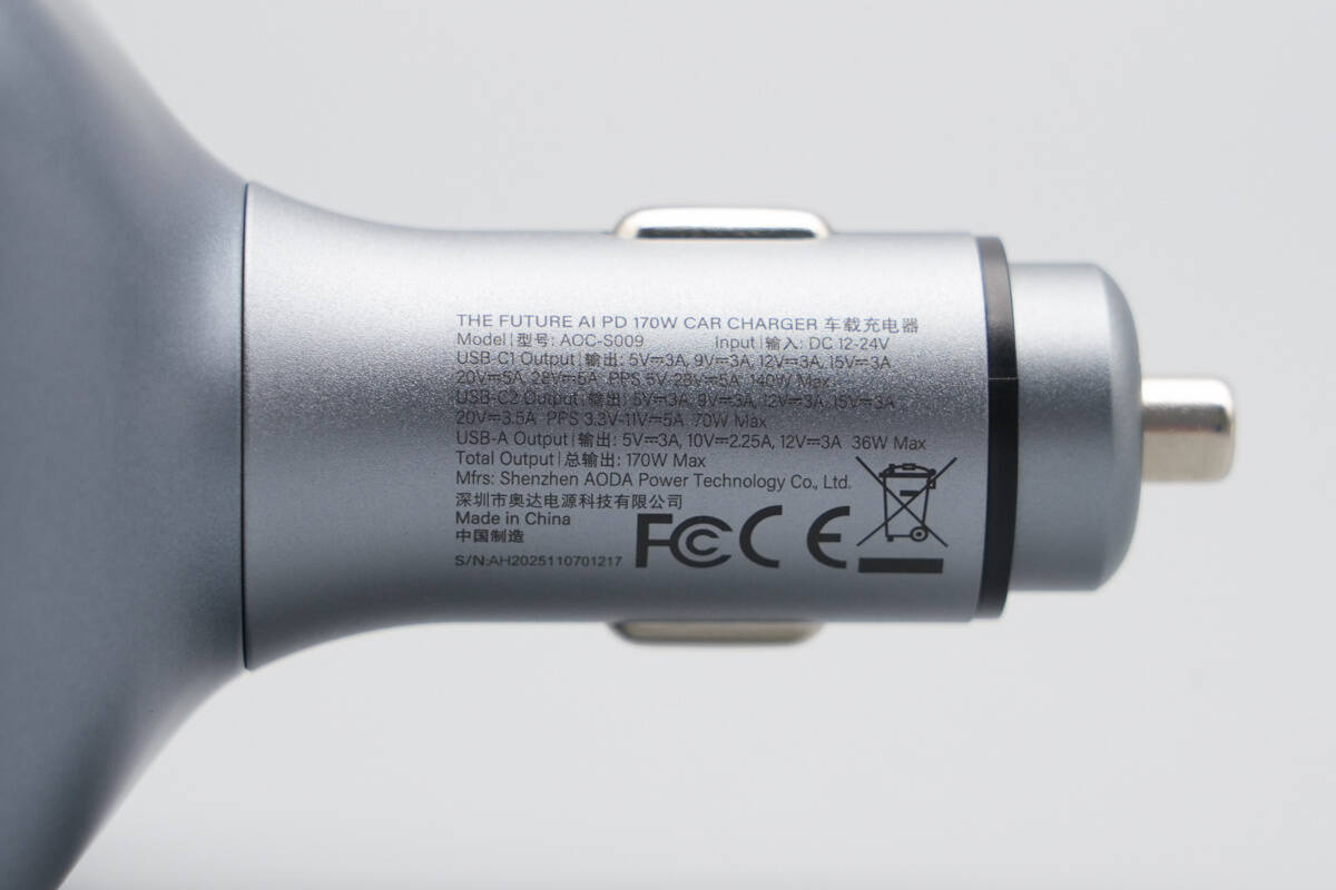
Product information is printed on the opposite side.
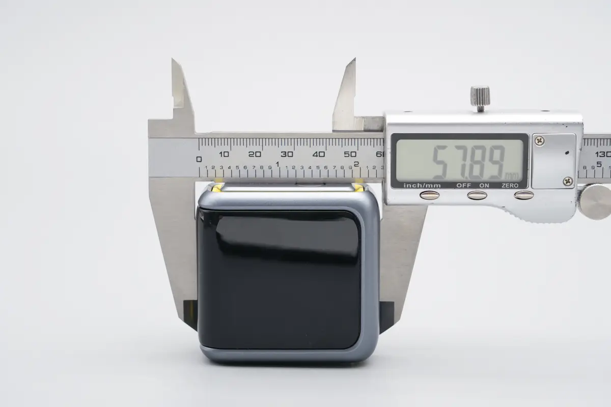
The length of the top section of the car charger is about 57.9 mm (2.28 inches).
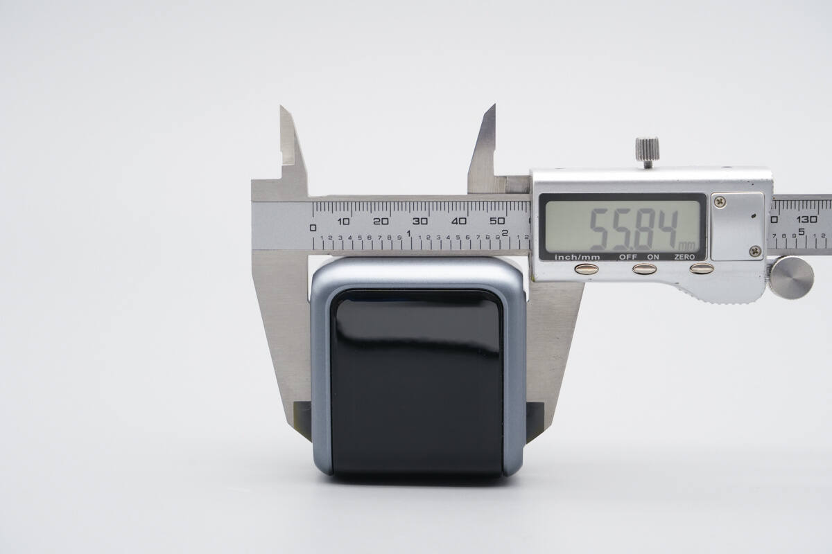
The width is about 55.8 mm (2.2 inches).
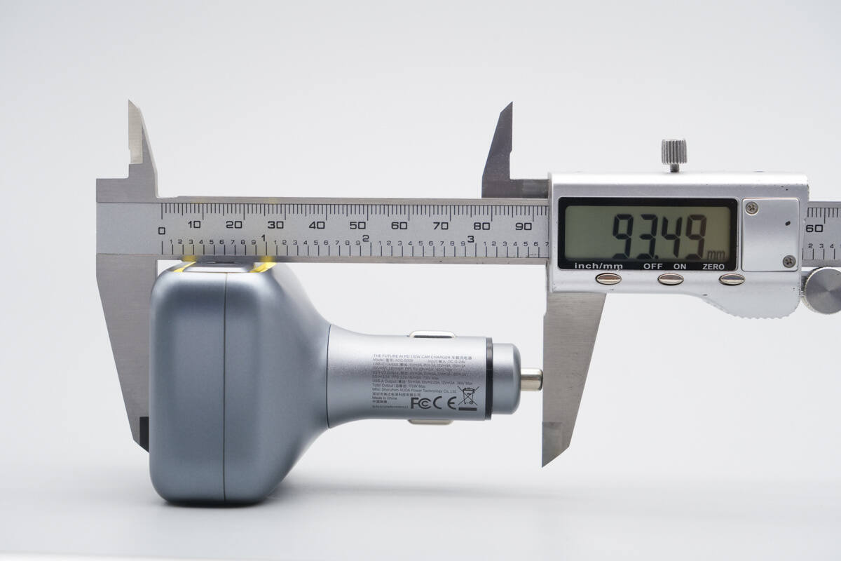
The overall length of the car charger is about 93.5 mm (3.68 inches).
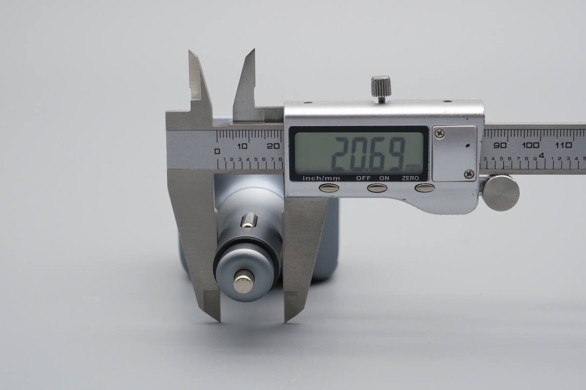
The diameter is about 20.7 mm (0.81 inches).
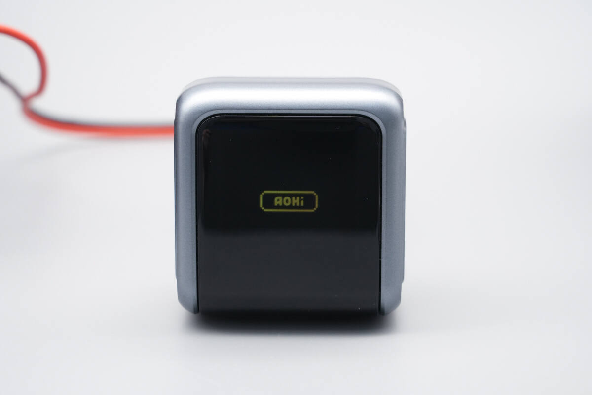
When power is applied, the AOHi logo is displayed.
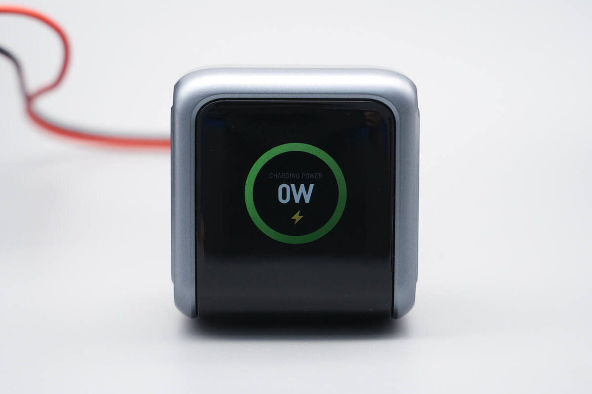
When no devices are connected, the display shows a total output power of 0W.
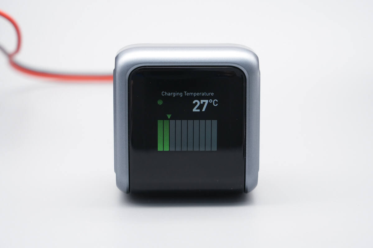
The display shows a temperature of 27°C.
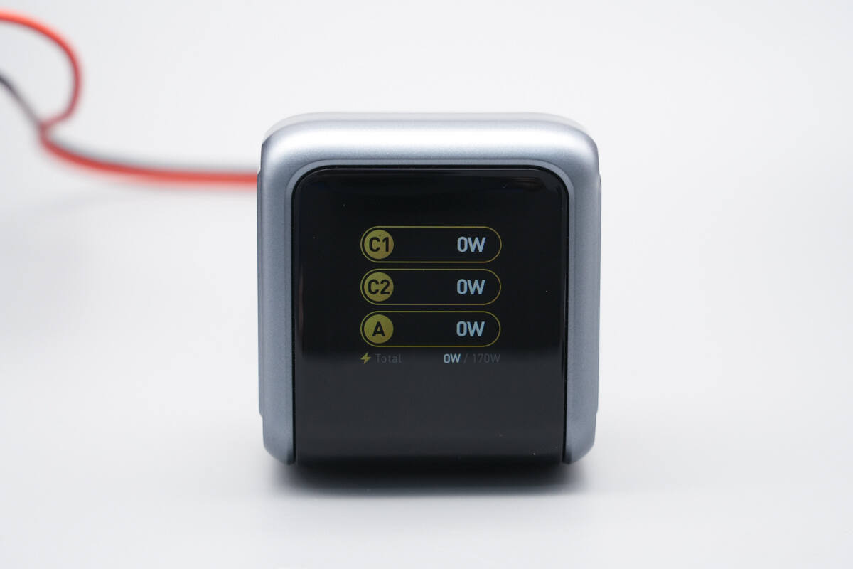
The display indicates that the output power of each port is 0W.
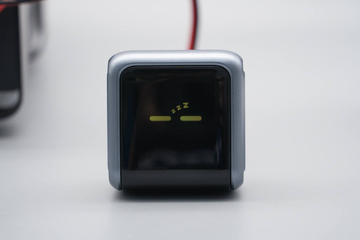
After a period of inactivity, the charger enters sleep mode.
That's how big it is on the hand.
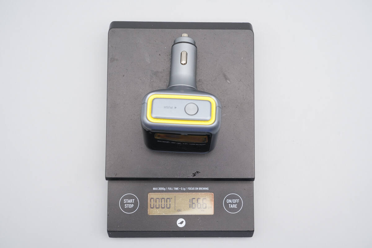
The weight is about 167 g (5.89 oz).
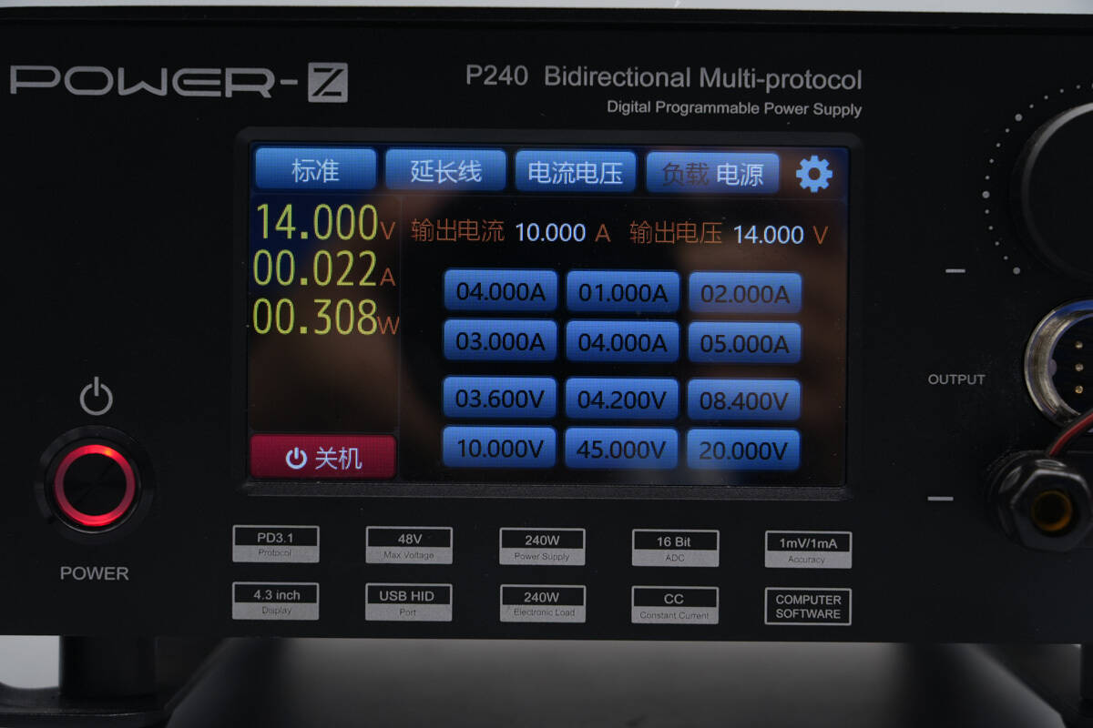
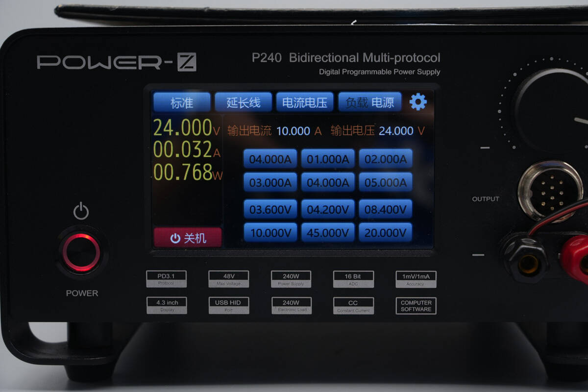
A POWER-Z P240 bidirectional multi-protocol power supply is used to power the car charger, with the output voltage set to 14V.
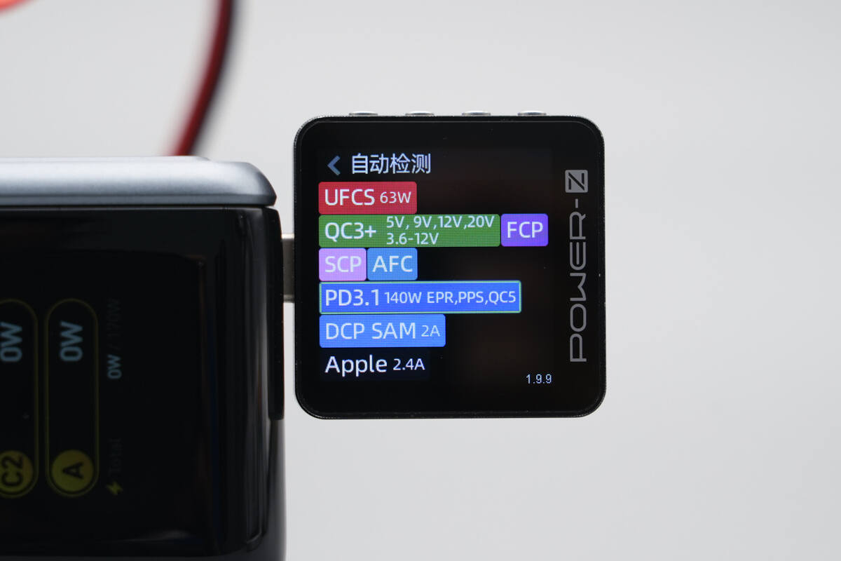
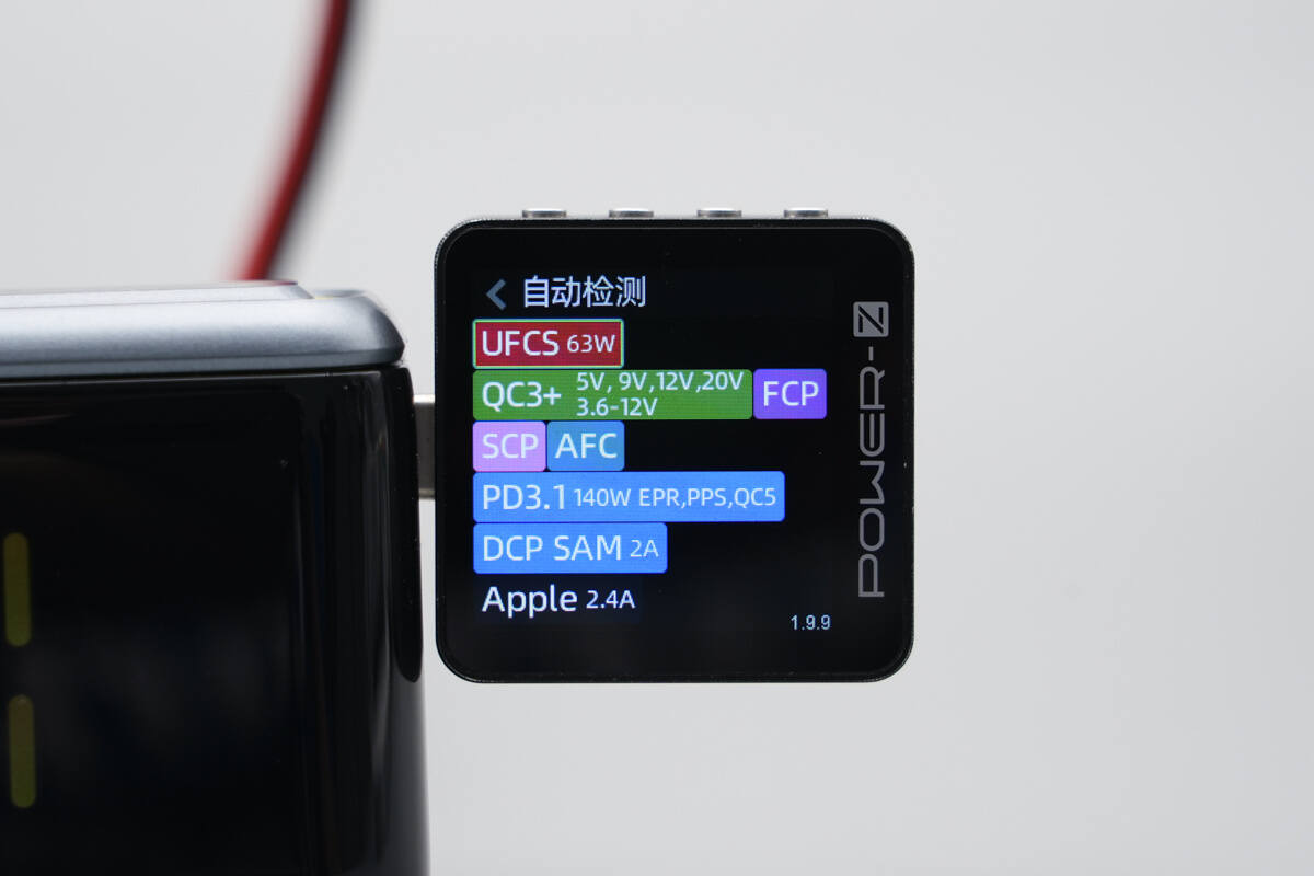
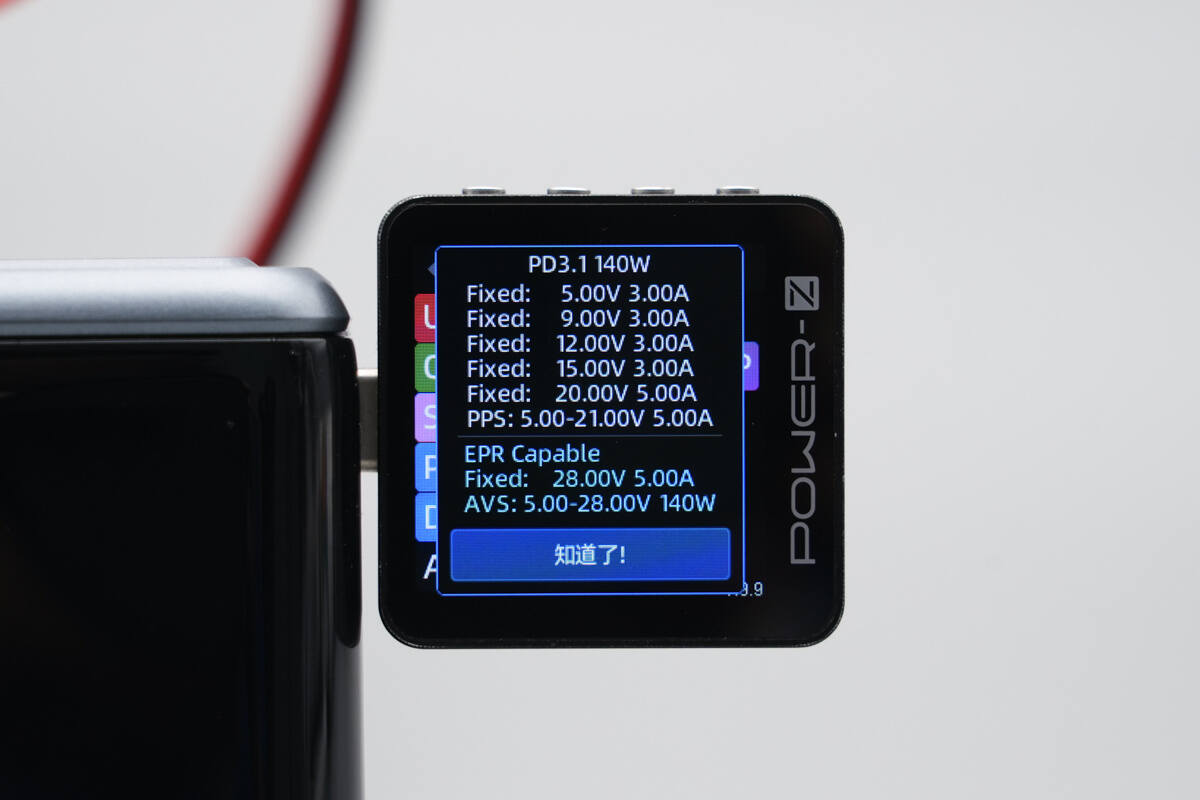
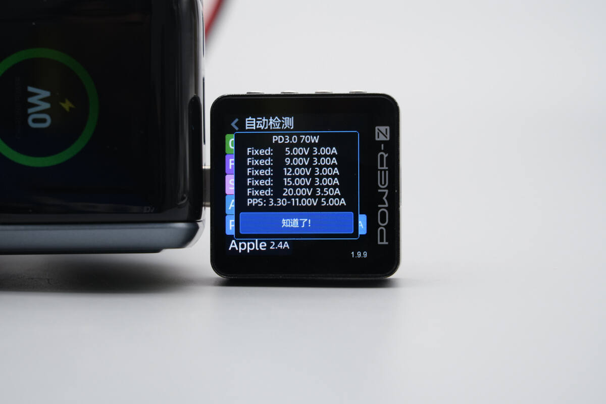
ChargerLAB POWER-Z KM003C shows that the USB-C1 supports QC3+/5, FCP, SCP, AFC, PD3.1, PPS, DCP, SAM 2A, and Apple 2.4A charging protocols.
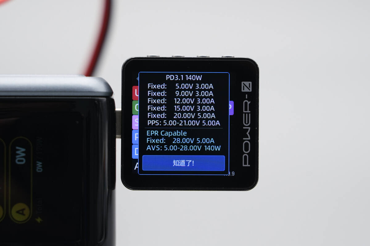
It features six fixed PDOs of 5V3A, 9V3A, 12V3A, 15V3A, 20V5A, and 28V5A, along with a 5–21V5A PPS voltage range and a 5–28V AVS voltage range.
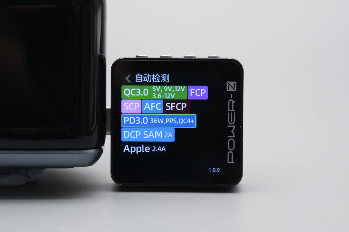
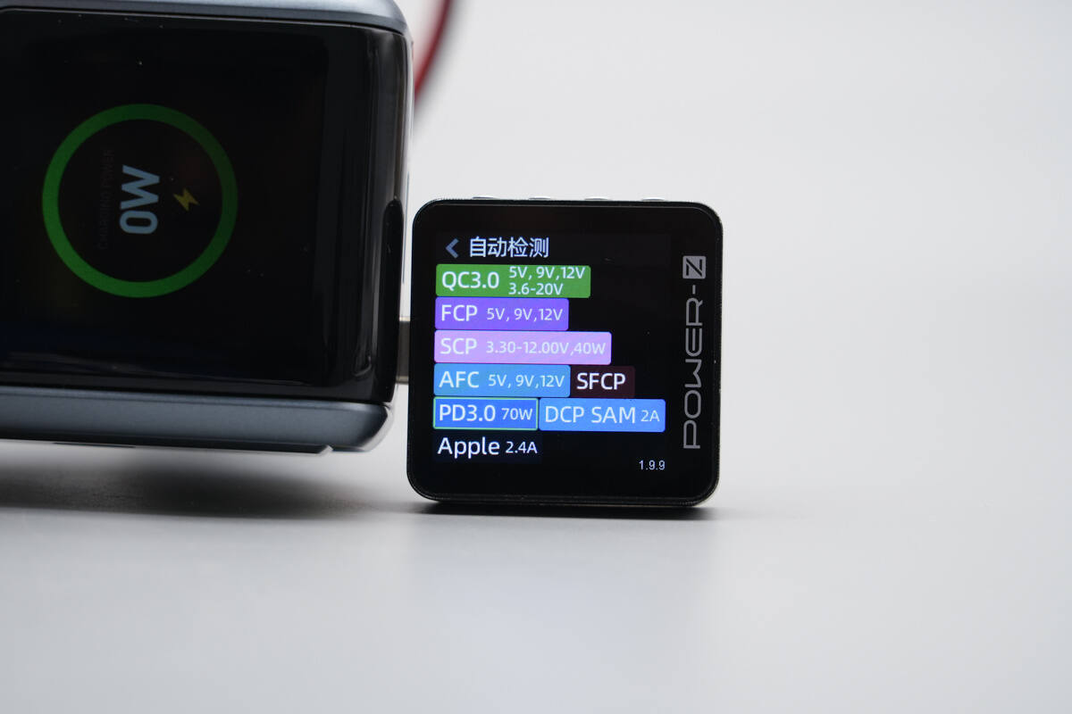
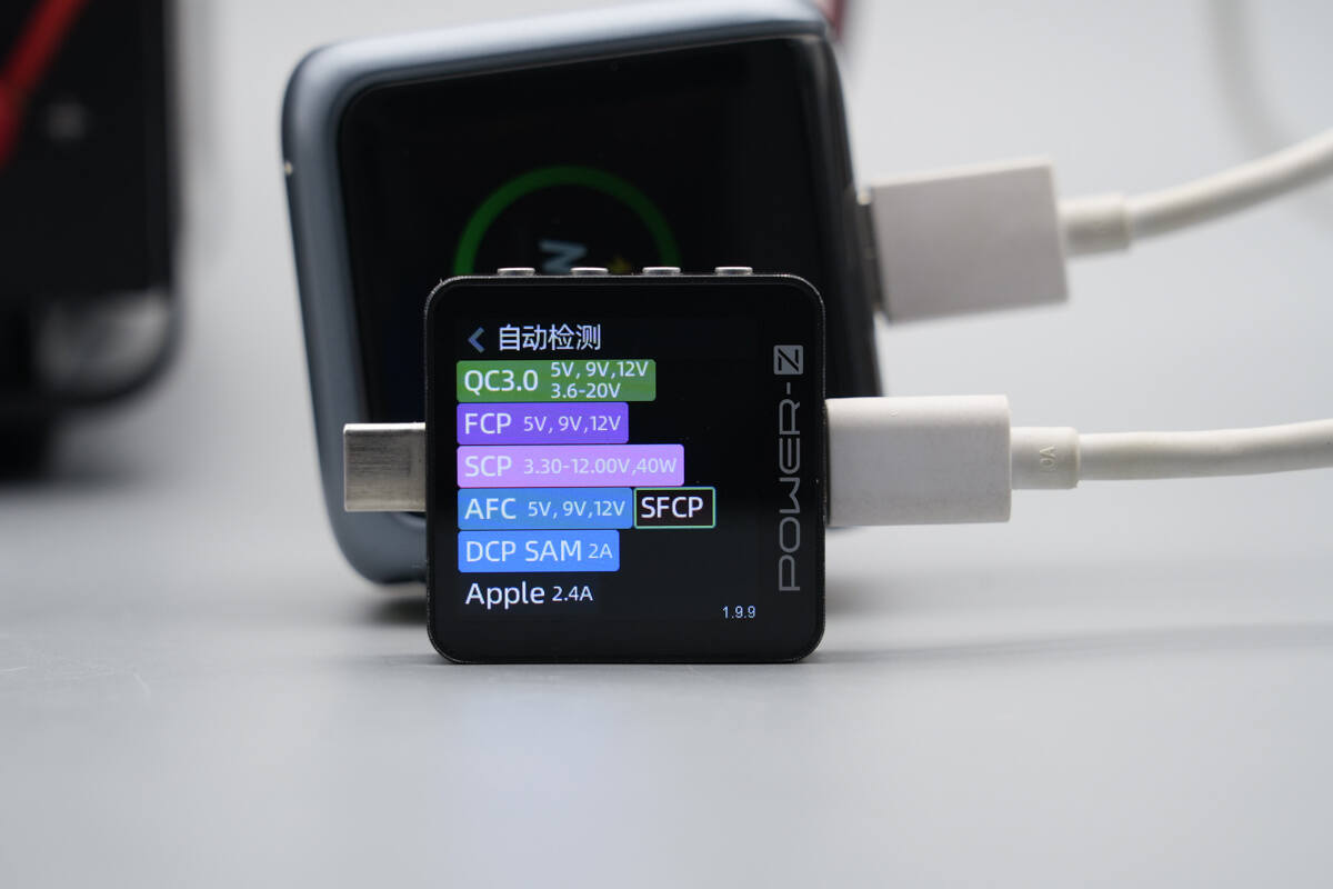
The USB-C2 supports QC3.0/4+, FCP, SCP, AFC, SFCP, PD3.0, PPS, DCP, SAM 2A, and Apple 2.4A charging protocols.
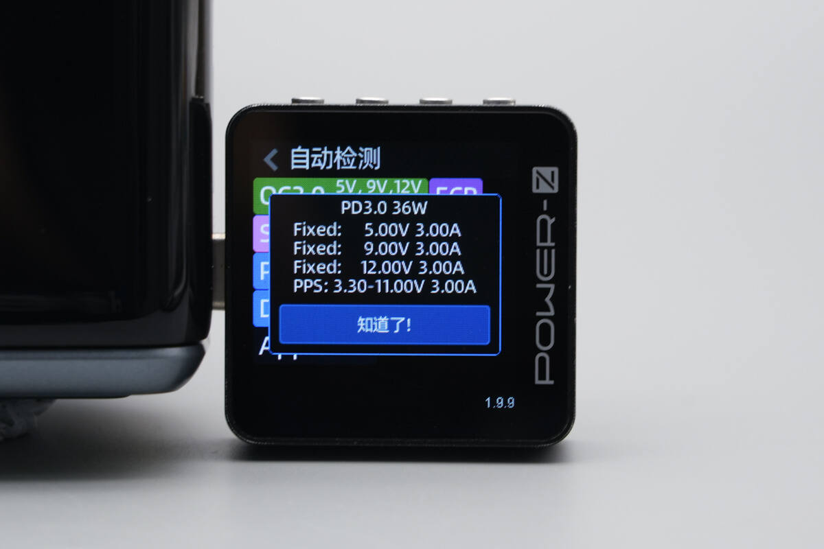
It has three fixed PDOs of 5V3A, 9V3A, and 12V3A, as well as one set of PPS, which is 3.3-11V3A.
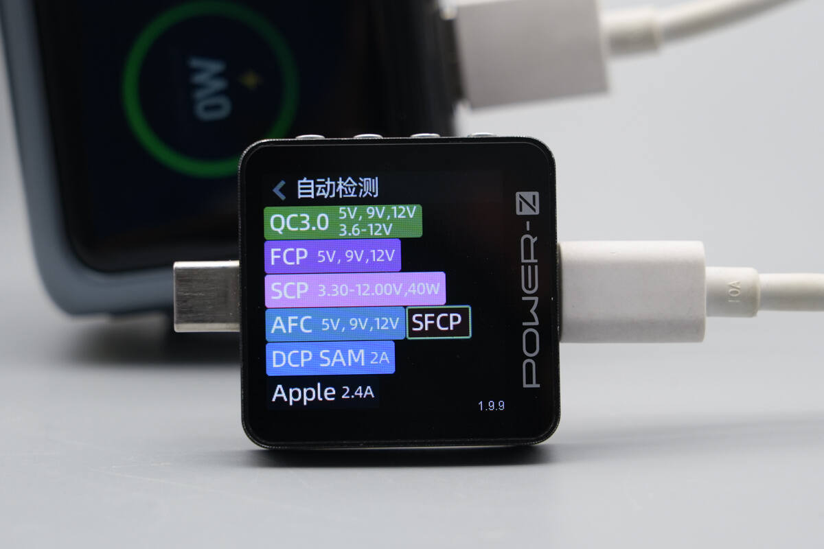
The USB-A supports QC3.0, FCP, SCP, AFC, SFCP, DCP, SAM 2A, and Apple 2.4A charging protocols.
The input voltage is adjusted to 24V.
After adjusting the input voltage, the output protocols of the USB-C1 port remain unchanged.
The PDO messages are also unchanged.
The USB-C2 supports QC3.0, FCP, SCP, AFC, SFCP, PD3.0, PPS, DCP, SAM 2A, and Apple 2.4A charging protocols.
It has five fixed PDOs of 5V3A, 9V3A, 12V3A, 15V3A, and 20V3.5A, as well as one set of PPS, which is 3.3-11V5A.
The supported protocols of the USB-A port also remain unchanged.
Teardown
Next, let's take it apart to see its internal components and structure.
The top panel, which is secured by snap-fit clips, is pried open.
Sealing foam is applied around the perimeter of the display.

The screws are removed, the wires are cut, and the housing is disassembled.
Close-up of the positive spring contact and the insulating washer.
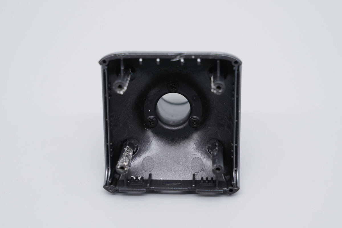
The plastic housing is provided with screw mounting holes.
Close-up of the negative contact spring.

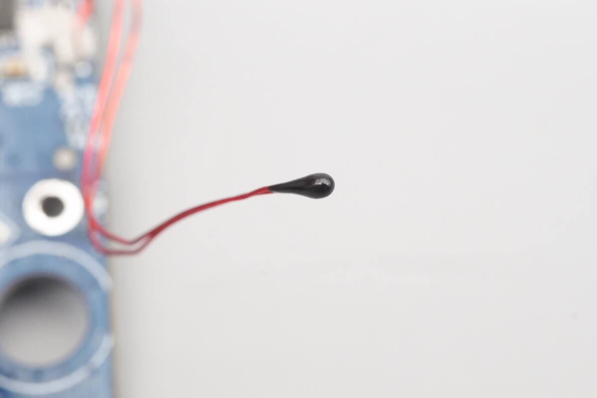
The wires pass through a ferrite bead and connect to the PCBA module, which is filled with thermal compound to enhance heat dissipation.
Close-upof the decorative cover plates on both sides of the housing.
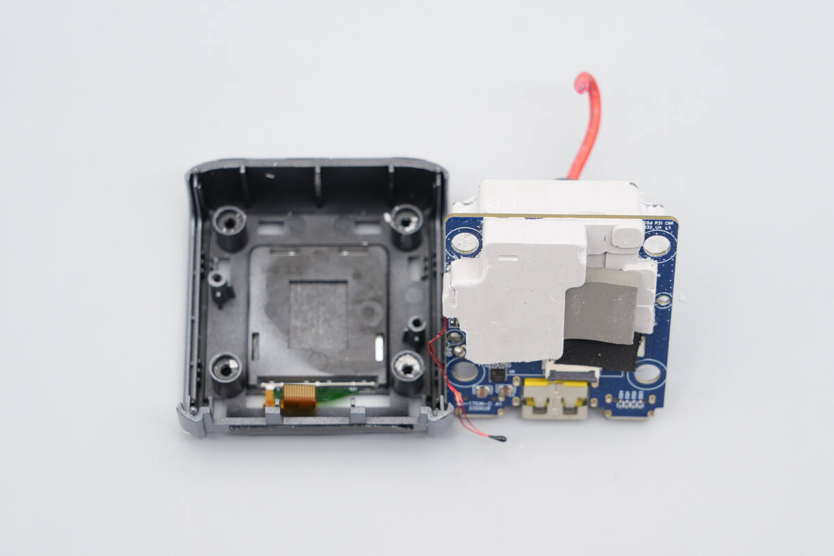
The PCBA module is removed from the housing.
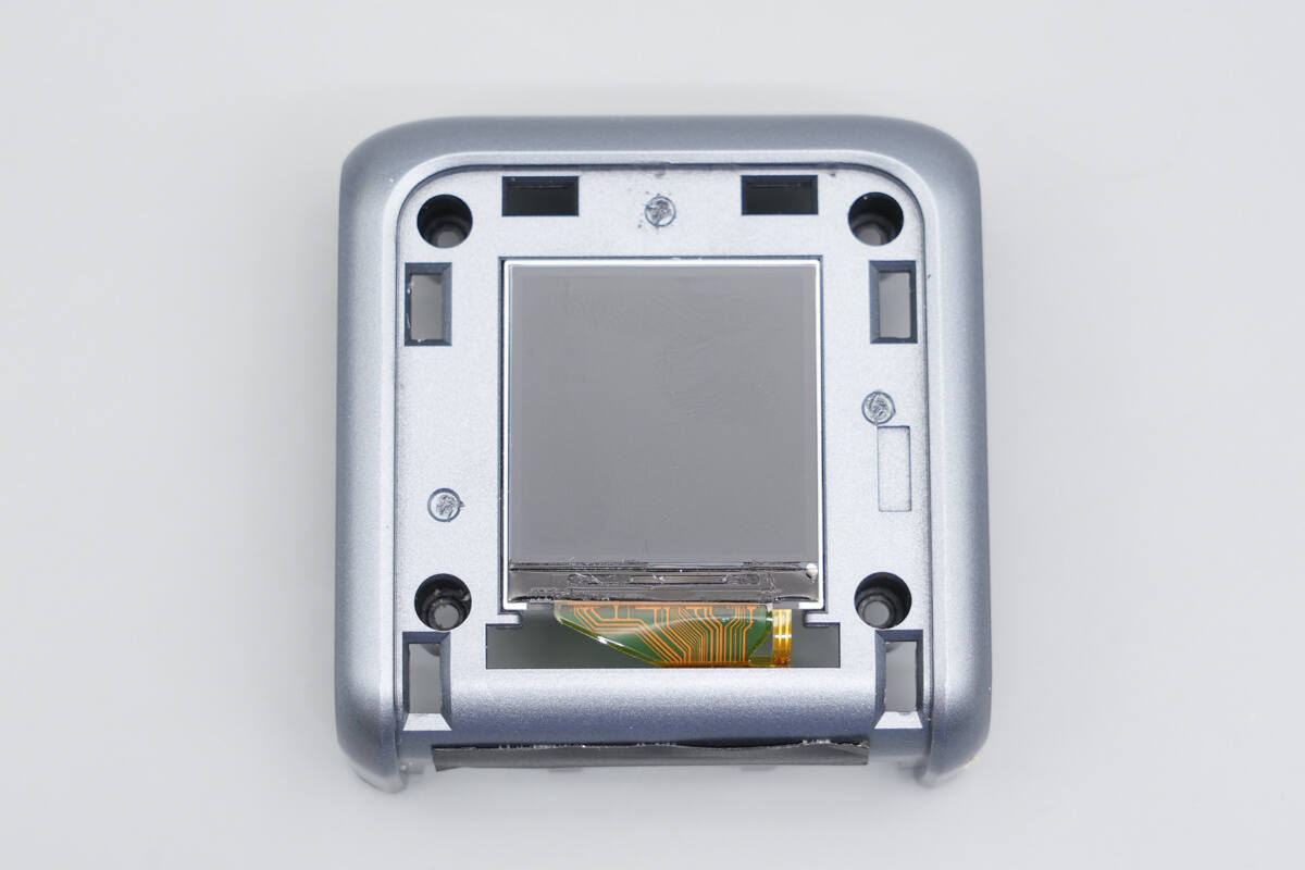
Inside the top cover, the display is secured and connected via a flexible ribbon cable.
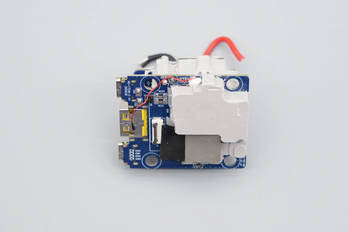
The front side of the PCBA module is also coated with thermal compound.
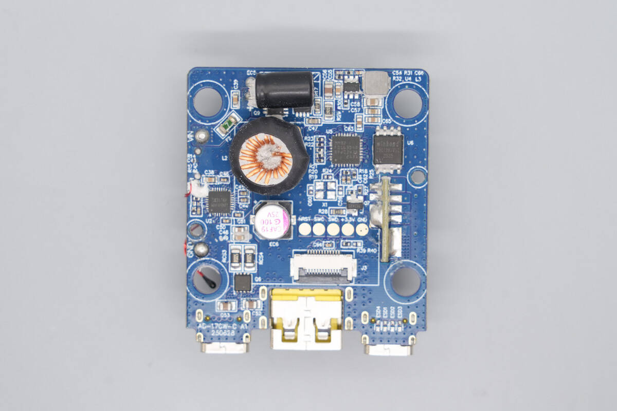
Remove the thermal compound. The front side of the PCBA module integrates an MCU, memory, a buck inductor, and a buck protocol controller chip.

The rear side is populated with synchronous buck-boost MOSFETs.
The side PCB carries a synchronous buck-boost controller, a protocol chip, and VBUS MOSFET.
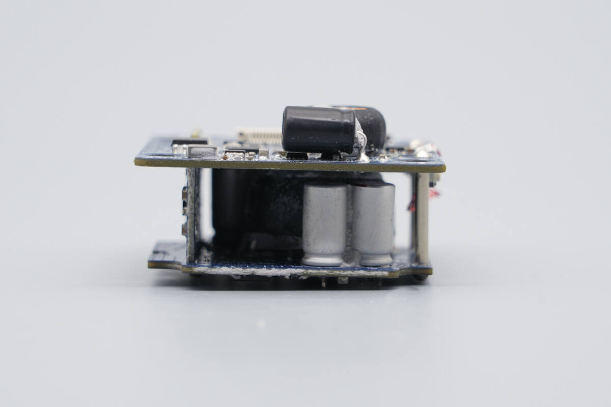
A buck-boost inductor and filtering capacitors are installed inside.
The module is powered via copper posts.
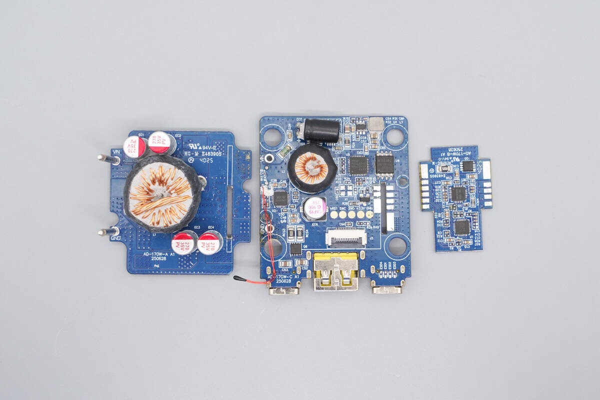
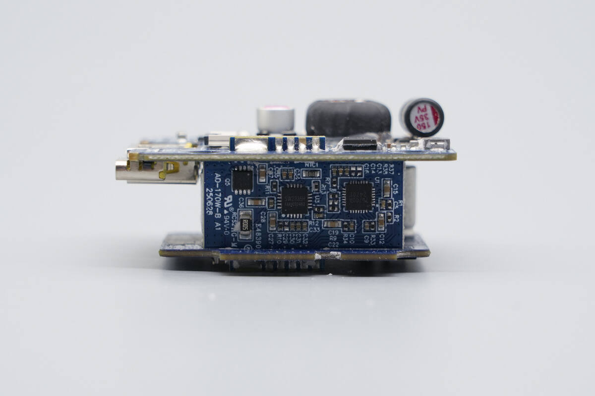
Separate the three small PCBs.
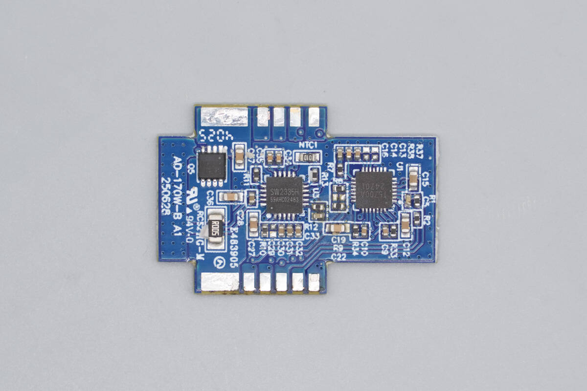
The small side PCB includes a synchronous buck-boost controller, a protocol chip, and a VBUS MOSFET.
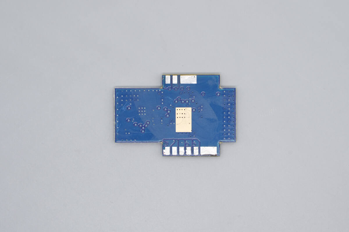
There are no components on the back side.
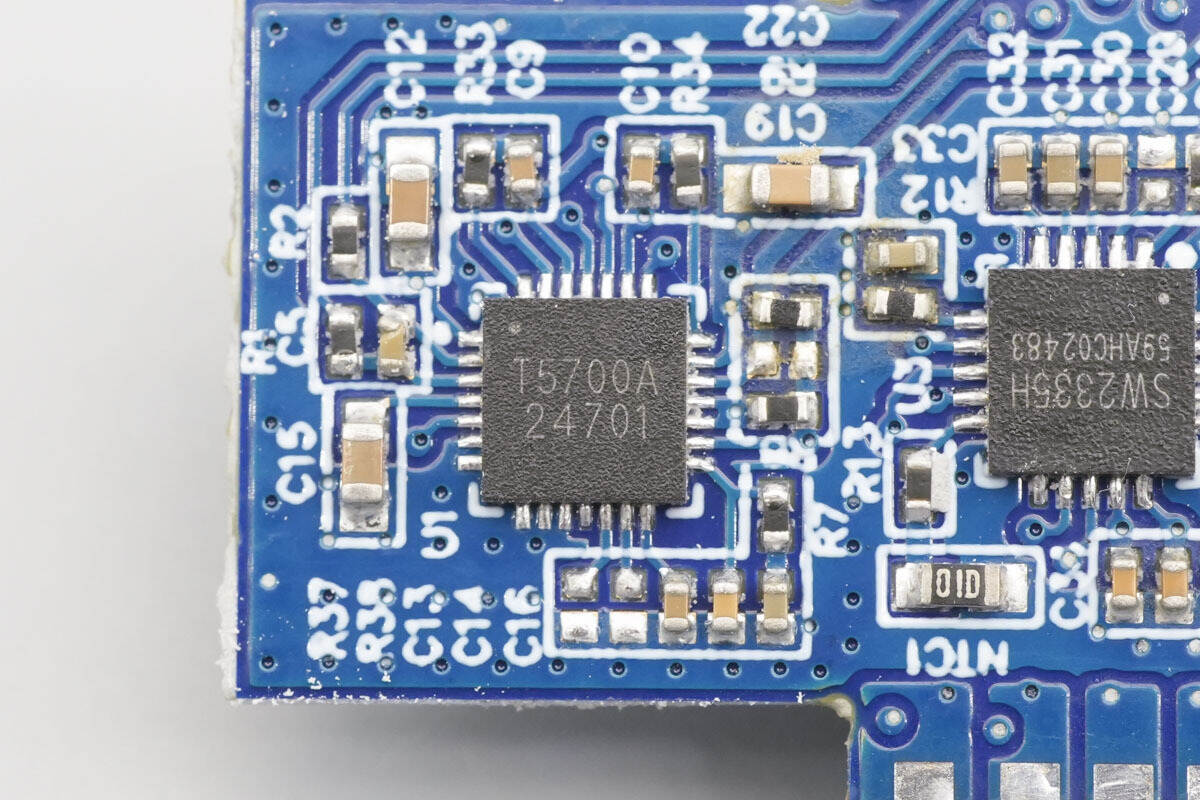
The synchronous buck-boost controller is from Tollsemi, model TMI5700A. It is a wide-range synchronous buck-boost controller with an I2C interface. The device uses peak current mode control and supports an input voltage range of 3.9–36 V and an output voltage range of 0.59–34 V, with a switching frequency from 150 kHz to 1 MHz. It integrates 6 V / 3 A gate drivers and supports adjustable input and output current limits. The controller features input undervoltage lockout, output short-circuit protection, output overvoltage protection, and thermal shutdown, and is packaged in a QFN-28 package.
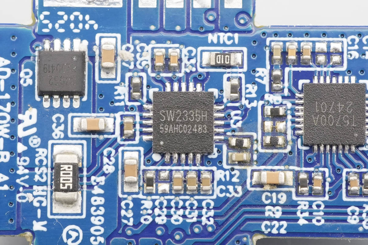
The protocol chip is from iSmartWare, model SW2335. It is a highly integrated fast-charging protocol controller featuring an embedded ARM Cortex-M0 CPU with a maximum frequency of up to 40 MHz. The device integrates 1 Mbit / 2 Mbit Flash memory and 4 KB SRAM, and supports both I2C Master/Slave and UART communication interfaces, providing strong processing capability for the system. In addition, it supports multiple GPIOs and a GPADC, and is designed with a strong focus on low power consumption to ensure energy-efficient operation. The SW2335 supports fast-charging protocols such as PD 3.1 and UFCS, supports output voltages up to 32 V, and is suitable for applications including car chargers and power adapters. It is packaged in a QFN-20 package.
Here is the information about iSmartWare SW2335.
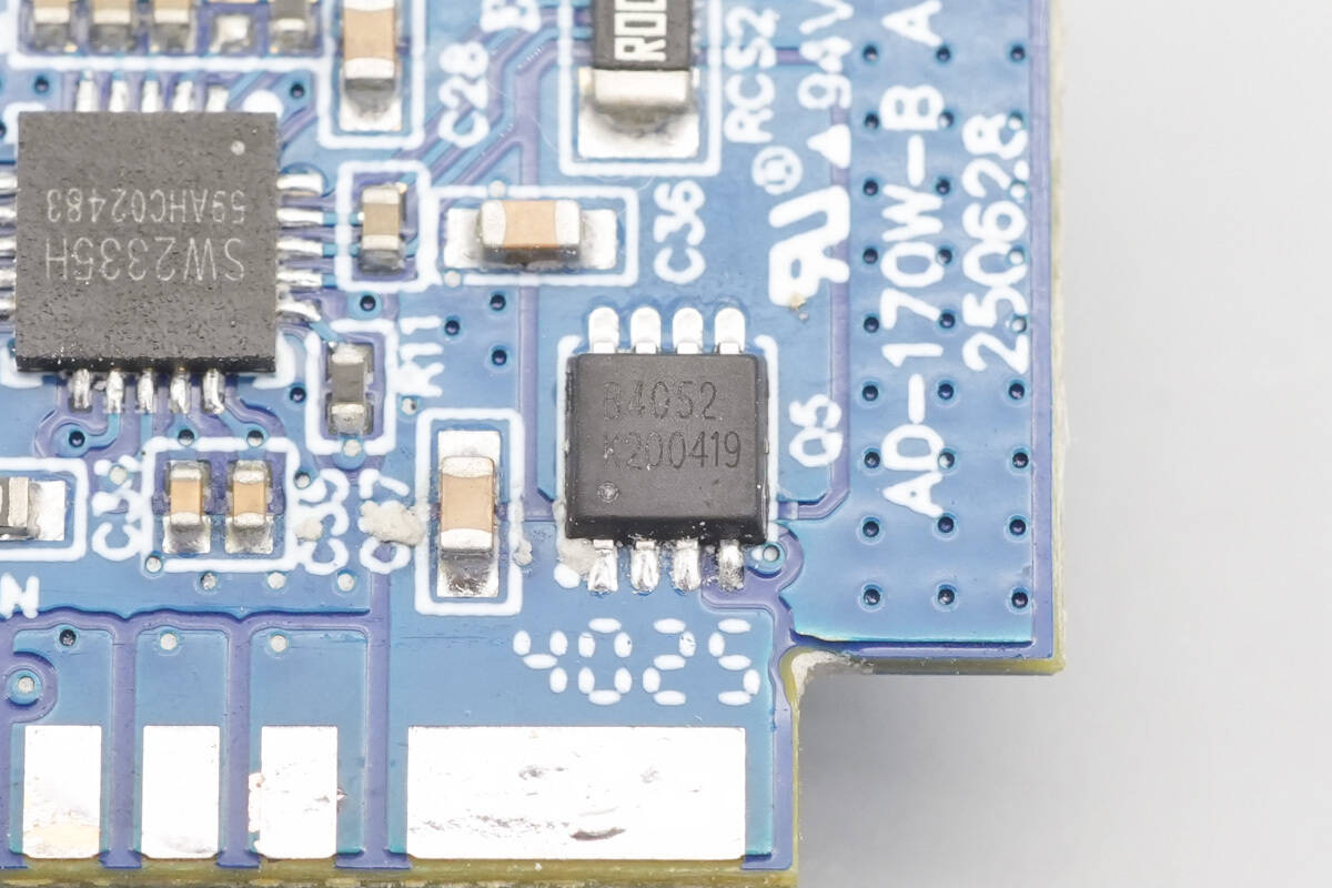
The VBUS MOSFET is marked “B4052” and is packaged in a DFN 3 × 3 package.
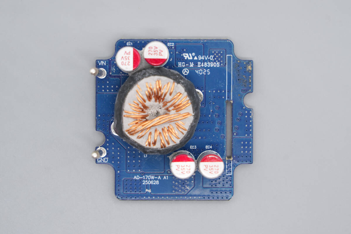
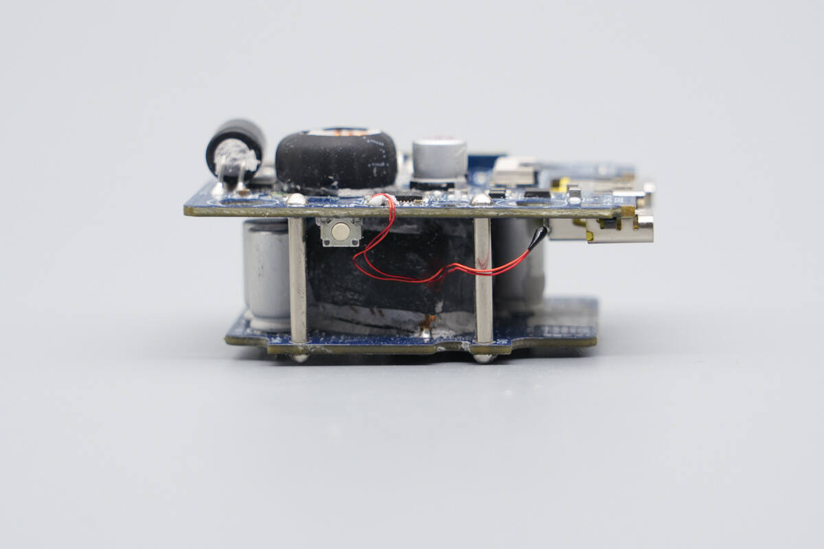
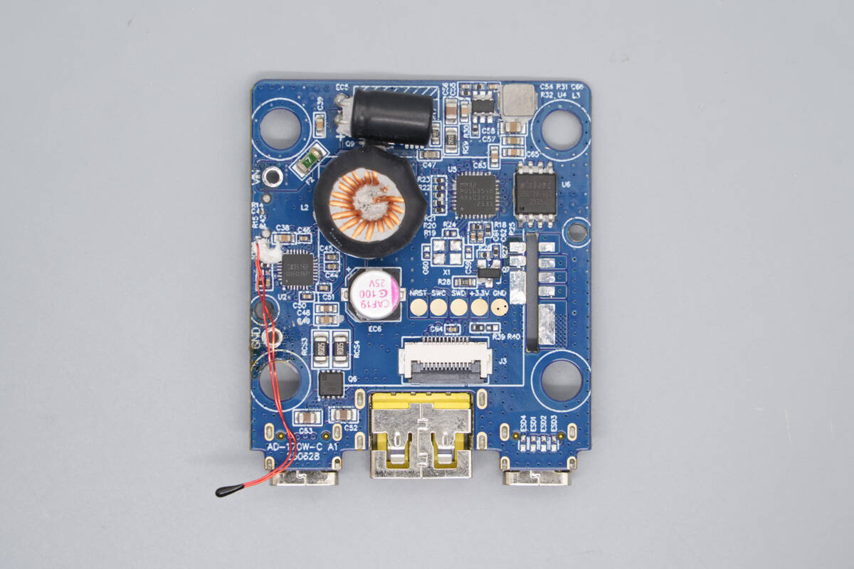
The bottom PCB contains a buck-boost inductor and solid-state capacitors.

The back side is equipped with synchronous buck-boost MOSFETs and a fuse.
A 15 A fuse is used for overcurrent protection.
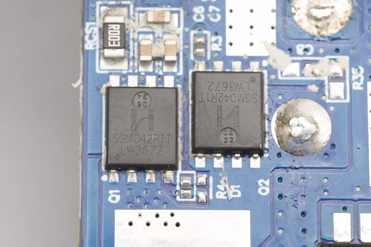
The synchronous buck-boost MOSFETs are from HI-SEMICON, model SGM042R1T. They are N-channel MOSFETs rated at 40 V, with an on-resistance of 1.8 mΩ, and are packaged in a PDFN 5 × 6-8L package.
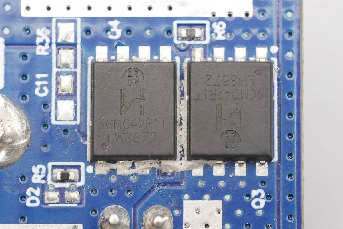
The other two MOSFETs are of the same model.
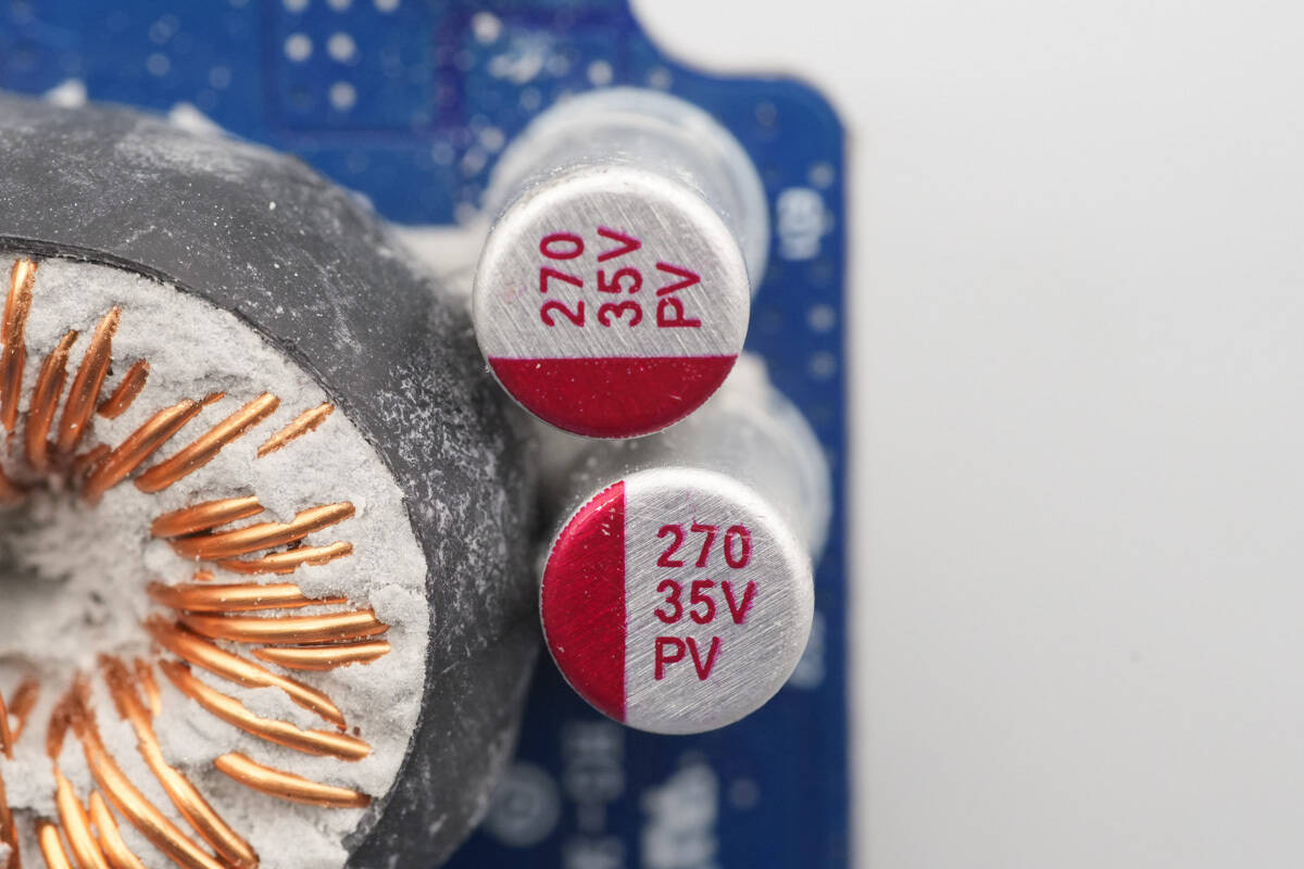
The input filter capacitors are rated at 270 μF, 35 V.
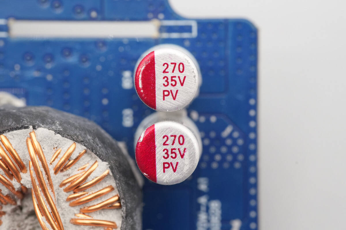
The output filter capacitors have the same specifications.
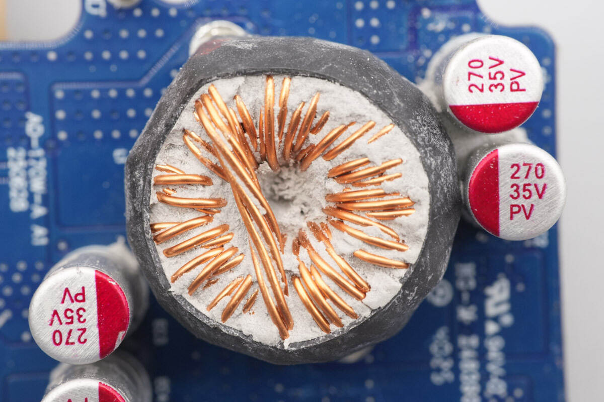
The buck-boost inductor is wound with multiple strands of enameled wire and insulated with a heat-shrink tubing sleeve.
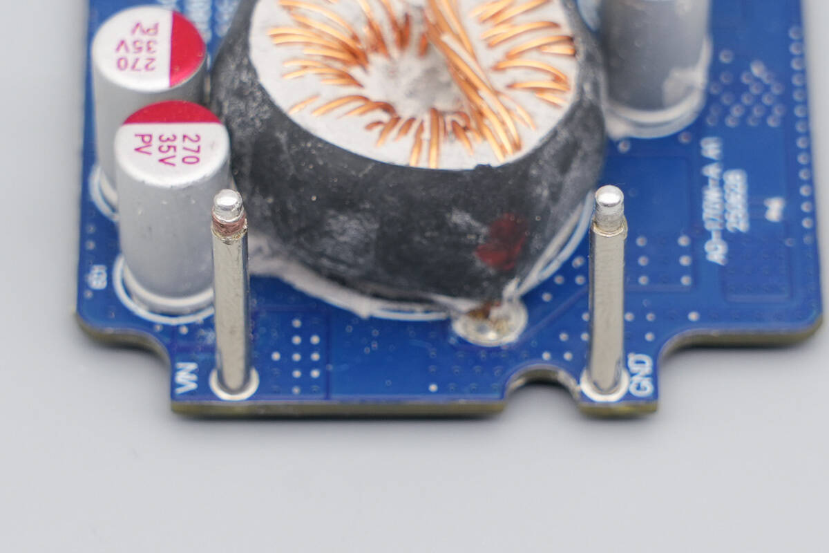
Two copper posts serve as the positive and negative terminals, providing power to the upper-layer PCBA module.
The upper-layer PCBA module includes a buck protocol chip, a VBUS MOSFET, an inductor, an input filter capacitor, a buck inductor, an output filter capacitor, synchronous buck MOSFETs, a synchronous buck controller, an additional buck inductor, an MCU, and memory.
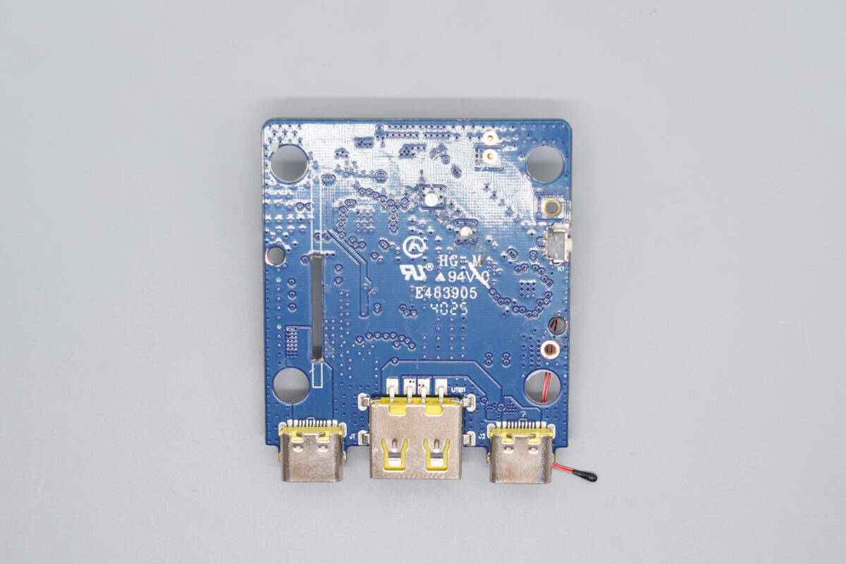
The back side is soldered with USB-C and USB-A sockets.
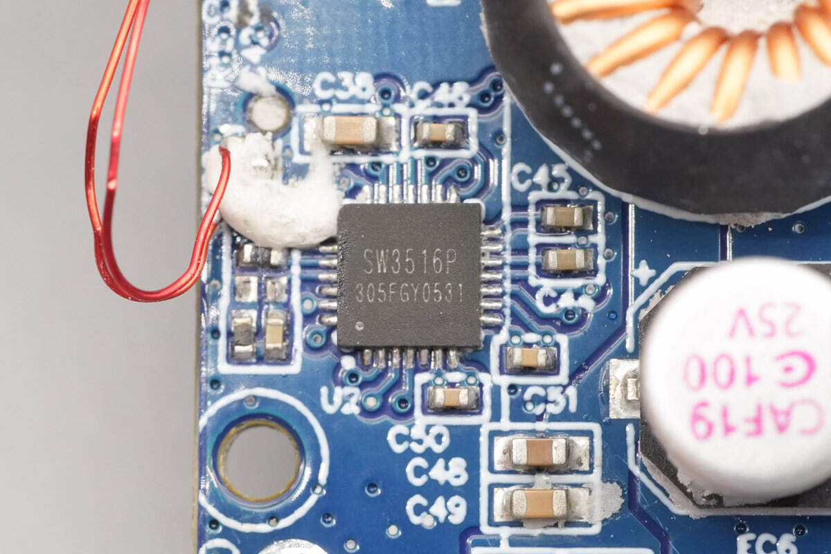
The buck protocol chip is from iSmartWare, model SW3516P. It is a highly integrated dual-port fast-charging protocol chip that supports fast charging on either the A or C port and allows independent current limiting for both ports. Its parameters and specifications are the same as the iSmartWare SW3516H. The SW3516P integrates a 5A high-efficiency synchronous buck converter.
It supports multiple fast-charging protocols, including PPS, PD, QC, AFC, FCP, SCP, PE, and SFCP, with a maximum PD output of 100 W. The chip features CC/CV operation modes and dual-port management logic. With minimal external components, it can form a complete high-performance dual-port fast-charging solution.
It is suitable for car chargers, adapters, and power strips, and integrates soft-start, input overvoltage protection, input undervoltage protection, output overcurrent protection, output short-circuit protection, and thermal shutdown. The chip also includes an I2C interface and is packaged in a QFN-28 package.
Here is the information about iSmartWare SW3516P.
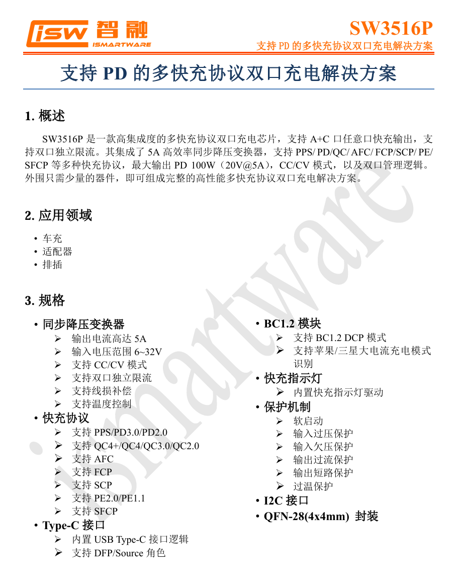
The two synchronous buck MOSFETs are marked “B4052.”
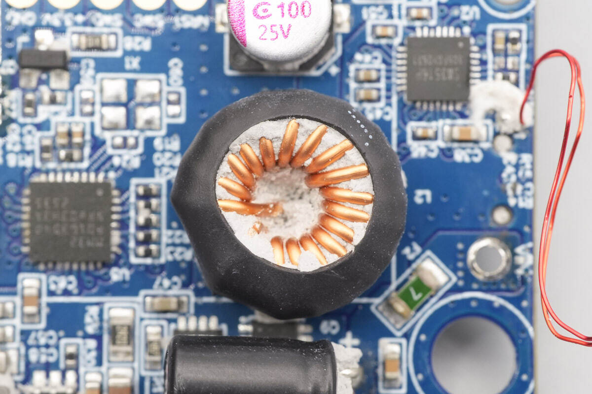
The buck inductor is insulated with heat-shrink tubing.
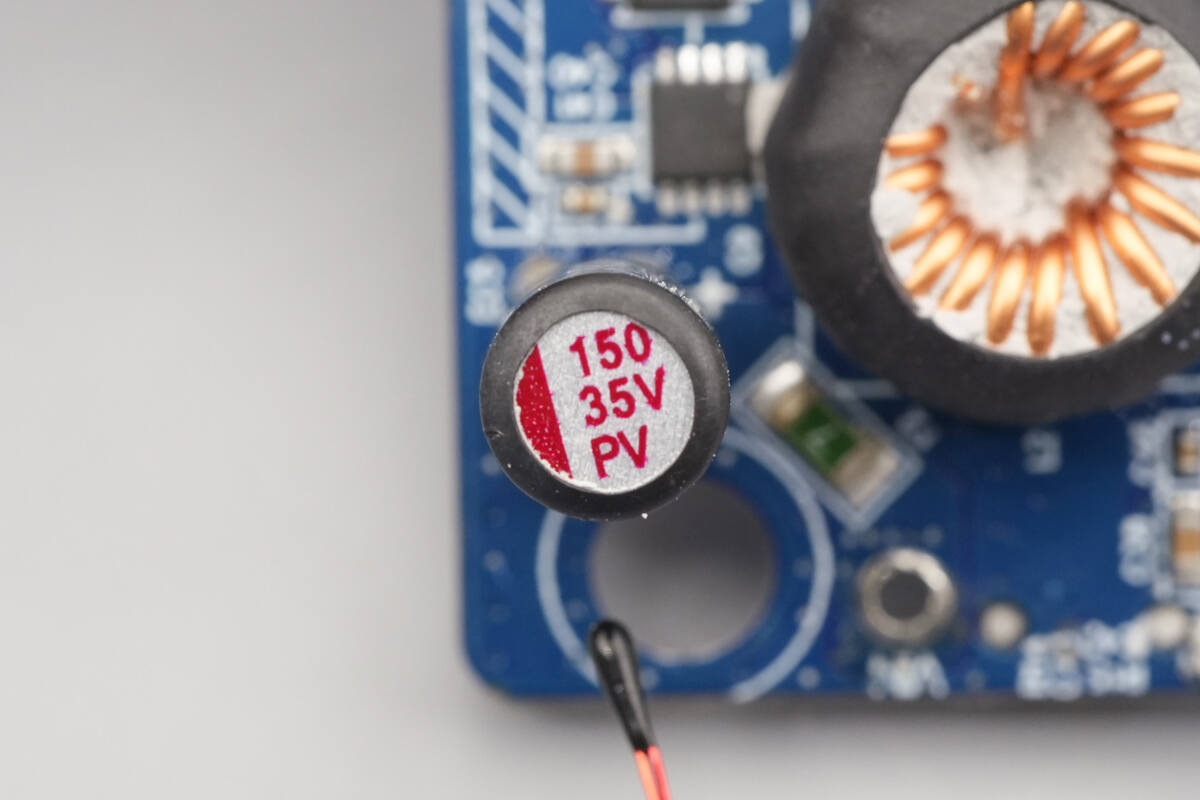
The input filter capacitor is rated at 150 μF, 35 V.
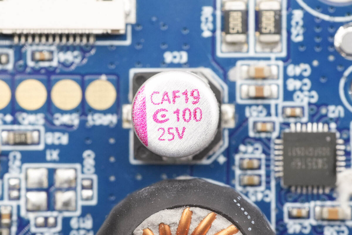
The output filter capacitors are from APAQ, rated at 100 μF, 25 V.
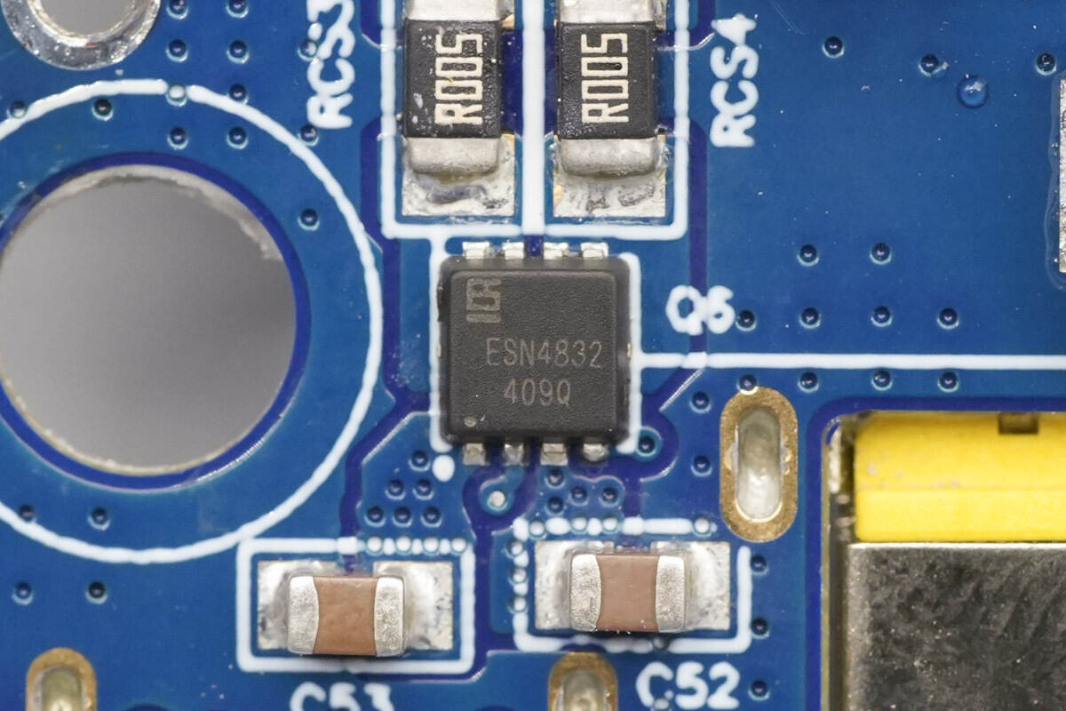
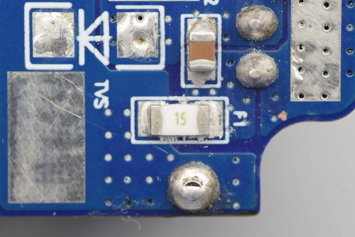
The VBUS MOSFET is from ElecSuper, model ESN4832. It is a dual N-channel MOSFET rated at 30 V, with an on-resistance of 11.5 mΩ, and is packaged in a PDFN 3 × 3-8L package.
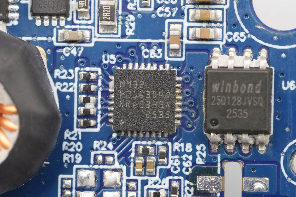
The MCU is from MindMotion, model MM32F0163D4Q. It features an embedded ARM Cortex-M0 core with a maximum operating frequency of 96 MHz, 128 KB Flash memory, and 16 KB SRAM. It provides UART, LPUART, I²C, I³C (slave) interfaces, SPI/I²S interfaces, and a USB interface. The MCU supports a 2–5.5 V operating voltage and is packaged in a QFN-32 package.
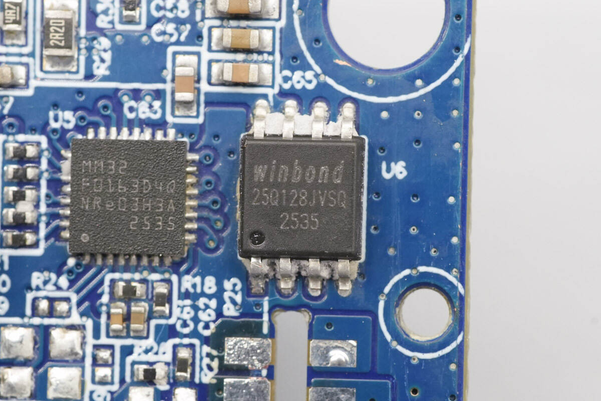
The memory is from Winbond, model W25Q128JVSIQ, with a capacity of 16 MB. It supports an operating voltage of 2.7–3.6 V and is packaged in an SOIC-8 package.
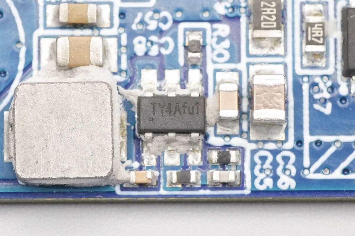
The synchronous buck chip is from Tollsemi, marked “TY4A,” model TMI3459. It is a synchronous buck converter with an input voltage range of 4.7–40 V and an output current of 0.6A. The chip integrates the MOSFETs internally, operates at a switching frequency of 2 MHz, and includes built-in compensation. It features overcurrent protection and thermal shutdown and is packaged in a SOT23-6 package.
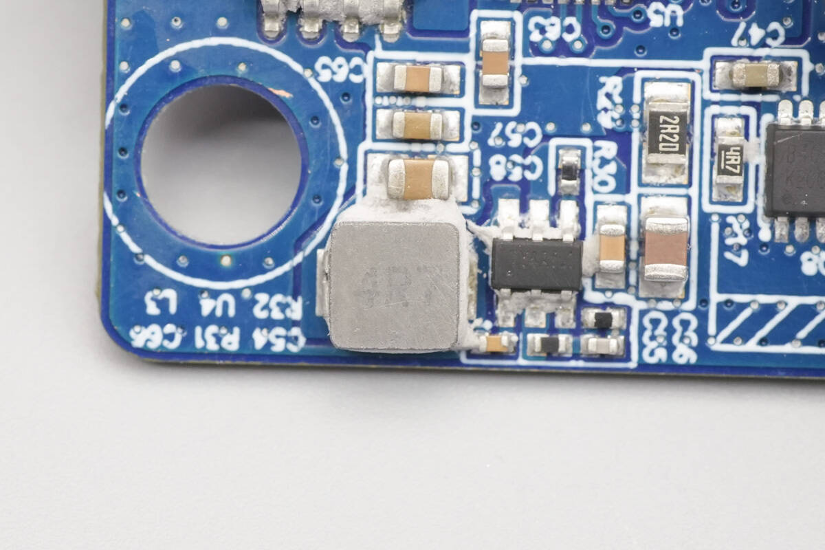
Close-up of the 4.7 μH buck inductor.
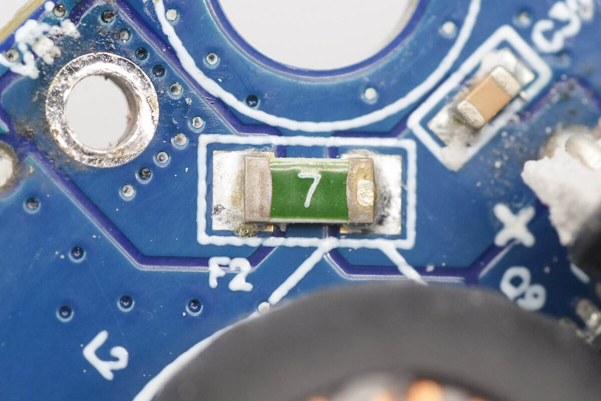
A 7A fuse is used for input overcurrent protection.
An NTC thermistor is used for temperature sensing.
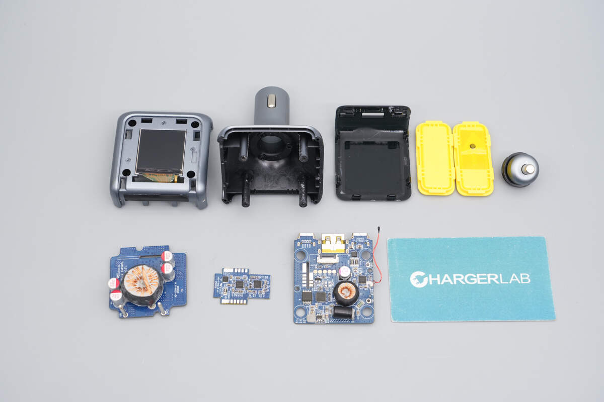
Well, those are all components of the AOHi THE FUTURE AI PD GaN+ 170W 3-Port LED Display Fast Car Charger.
Summary of ChargerLAB
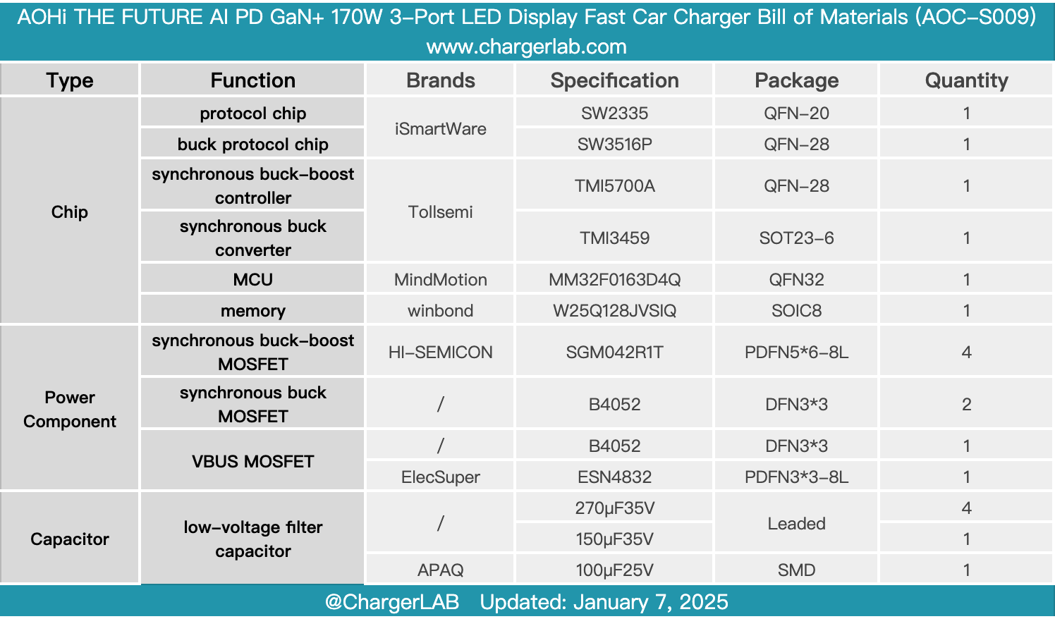
Here is the component list of the AOHi THE FUTURE AI PD GaN+ 170W 3-Port LED Display Fast Car Charger for your convenience.
It features two USB-C ports and one USB-A port, supporting 140 W PD3.1, 100 W PPS, and automatic power distribution of 100W + 70W. The LCD screen can display the output power of each port as well as the car charger’s temperature.
After taking it apart, we found that it contains one synchronous buck-boost circuit and one buck circuit. The synchronous buck-boost circuit uses an iSmartWare SW2335 protocol chip paired with a Tollsemi TMI5700A buck-boost controller, together with HI-SEMICON SGM042R1T synchronous buck-boost MOSFETs, supporting PD 3.1 140 W output.
The buck circuit uses an iSmartWare SW3516P protocol buck chip. A MindMotion MM32F0163D4Q MCU is integrated for parameter acquisition and overall system control, paired with a Winbond W25Q128JVSIQ memory. A Tollsemi TMI3459 supplies buck power to the MCU and the display. Internally, multiple PCBs are stacked and soldered together, with thermal adhesive encapsulation to enhance heat dissipation. The device demonstrates solid and reliable component selection and workmanship.
Related Articles:
1. Teardown of Torras FlexLine 67W Charger (CQ10)
2. Teardown of Anker Prime 150W Charging Station (A1903)
3. Teardown of Anker Prime 160W Charger with Smart Display (A2687)