Introduction
Anker has launched the Anker Prime 150W Charging Dock, a product that serves not only as a desktop charger but also as a fast charging station for portable power banks. The specially designed Pogo Pin contact array enables Anker's Prime series power banks, such as the 200W and 250W models, to charge automatically when placed on the dock, delivering up to 150W of charging power. This offers both convenience and efficiency while also increasing the number of devices that can be charged simultaneously on the desktop.
Additionally, the product supports both Bluetooth and Wi-Fi dual-mode wireless connectivity, allowing users to manage the charging dock and connected power banks via a smartphone app. The app provides real-time monitoring of power output, device temperature, and current battery level, along with customizable settings, enhancing the overall user experience.
The Anker Prime 150W Charging Dock is equipped with two USB-C ports and one USB-A port, making it compatible with various fast charging protocols such a QC, PD, PPS, and SCP. It also supports 140W PD3.1 fast charging, offering full-speed charging capabilities for devices like the MacBook Pro. Next, we will take a closer look at the detailed design of this product.
Product Appearance
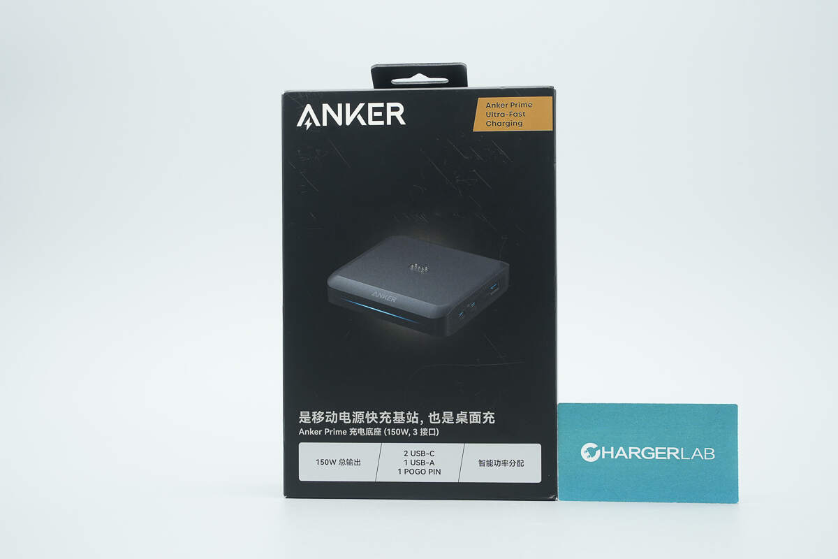
The front of the packaging box features the Anker logo, along with the product's appearance, name, and key selling points.
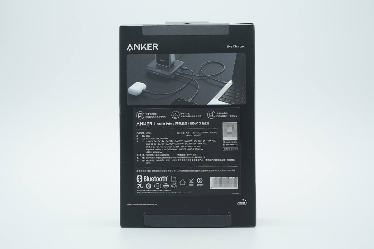
The back of the packaging features usage scenario images and includes a sticker with technical specifications.
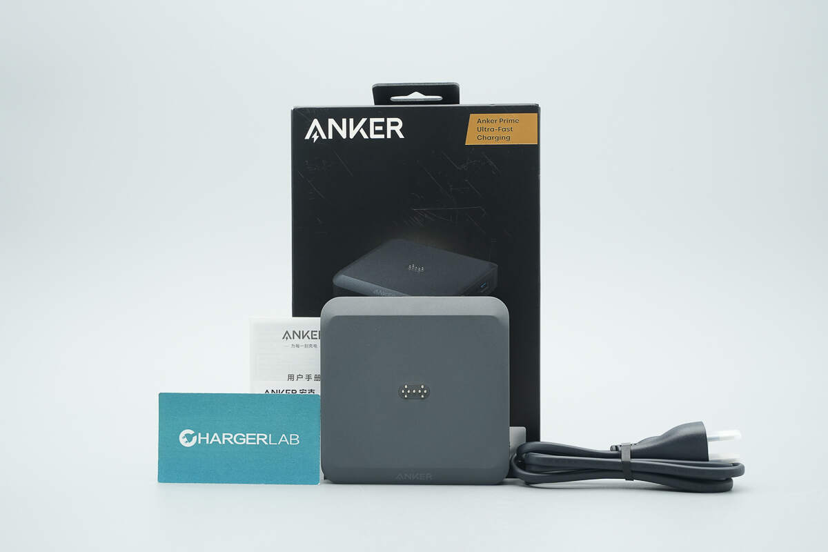
The package includes the Anker Prime 150W Charging Dock, a power cable, and a user manual.
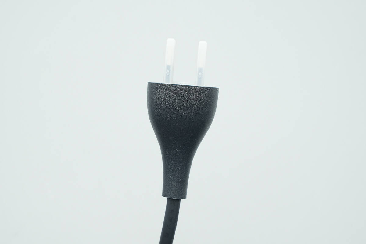
The power cable comes with a two-prong plug, and the prongs are protected with a plastic cover.
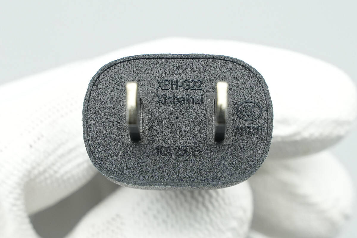
The power cable is rated at 10A 250V~, and it has passed the CCC certification.
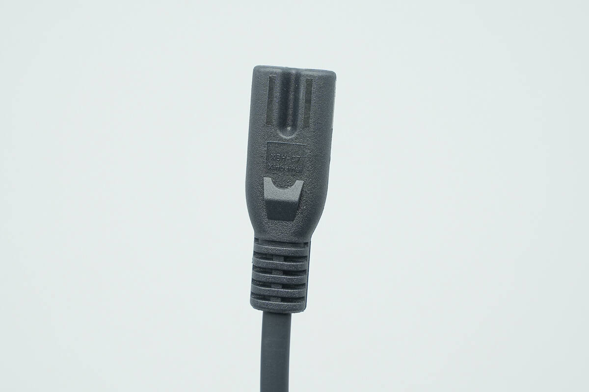
The other end of the cable features a figure-eight plug, with terminals designed for bend resistance and easy insertion and removal.
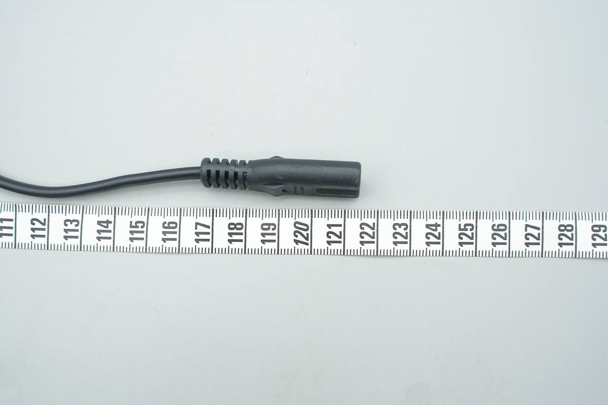
The length of the power cable is about 121.5 cm (47.83 inches).
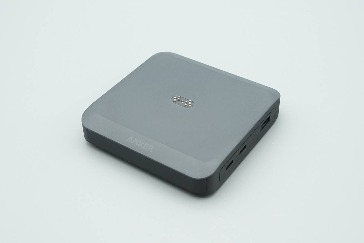
The body has a flat design, with beveled edges at the front and back of the top surface, giving it a minimalist style. The surface is matte, resistant to fingerprints and sweat stains, and can be easily cleaned with a wipe.
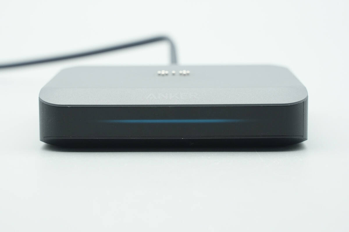
When powered on or connected to a specific Anker power bank, the front of the dock will feature a corresponding breathing light effect, with the light glowing blue.
The center of the beveled edge at the front is engraved with the Anker logo.
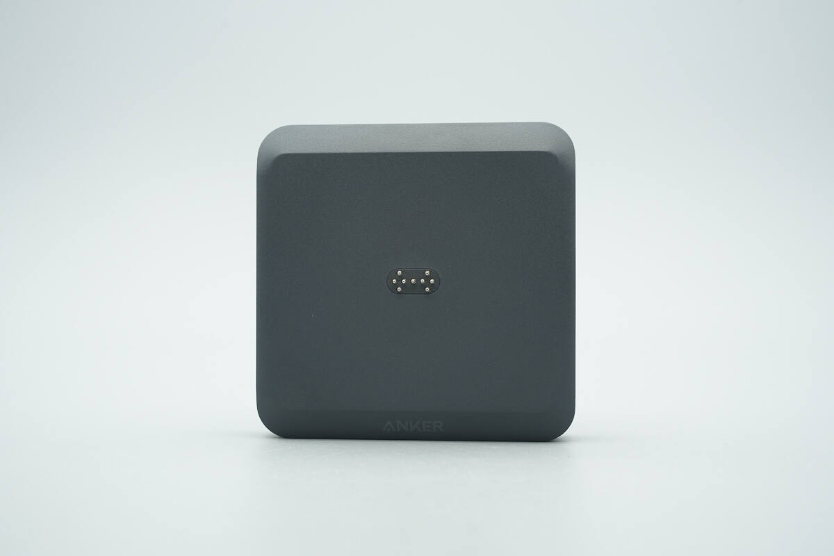
The center of the top surface is equipped with a Pogo Pin array.
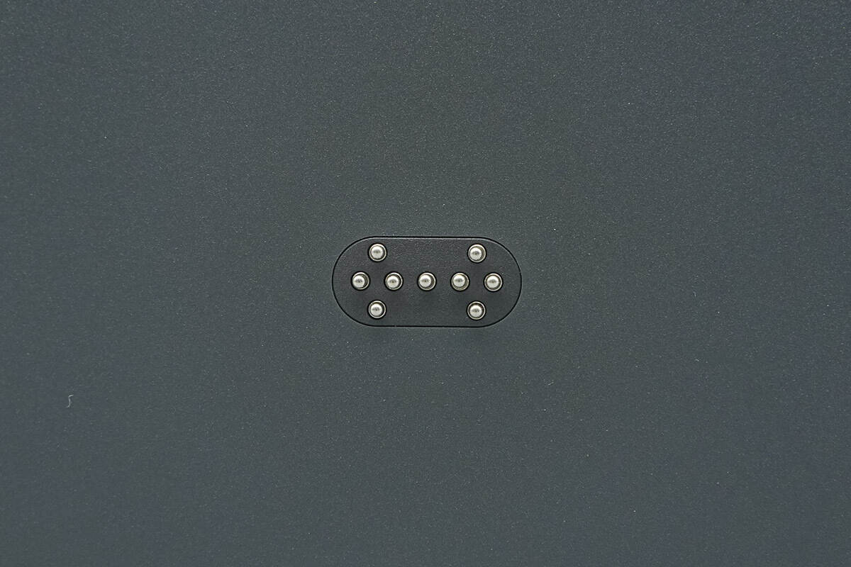
The Pogo Pin array features a magnetic design, allowing the power bank to automatically align and attach when brought close.
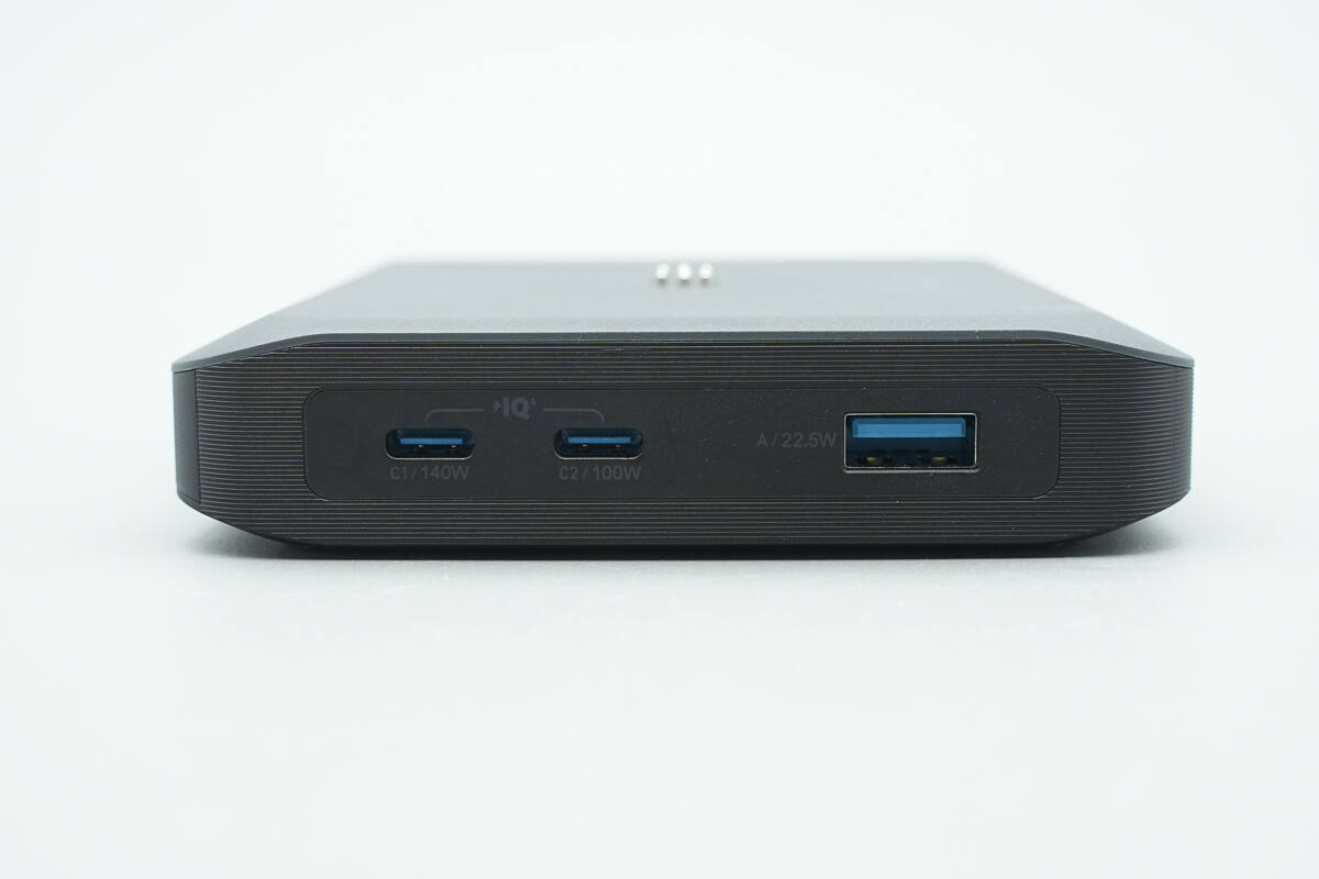
On this side of the body, there are two USB-C ports and one USB-A port.
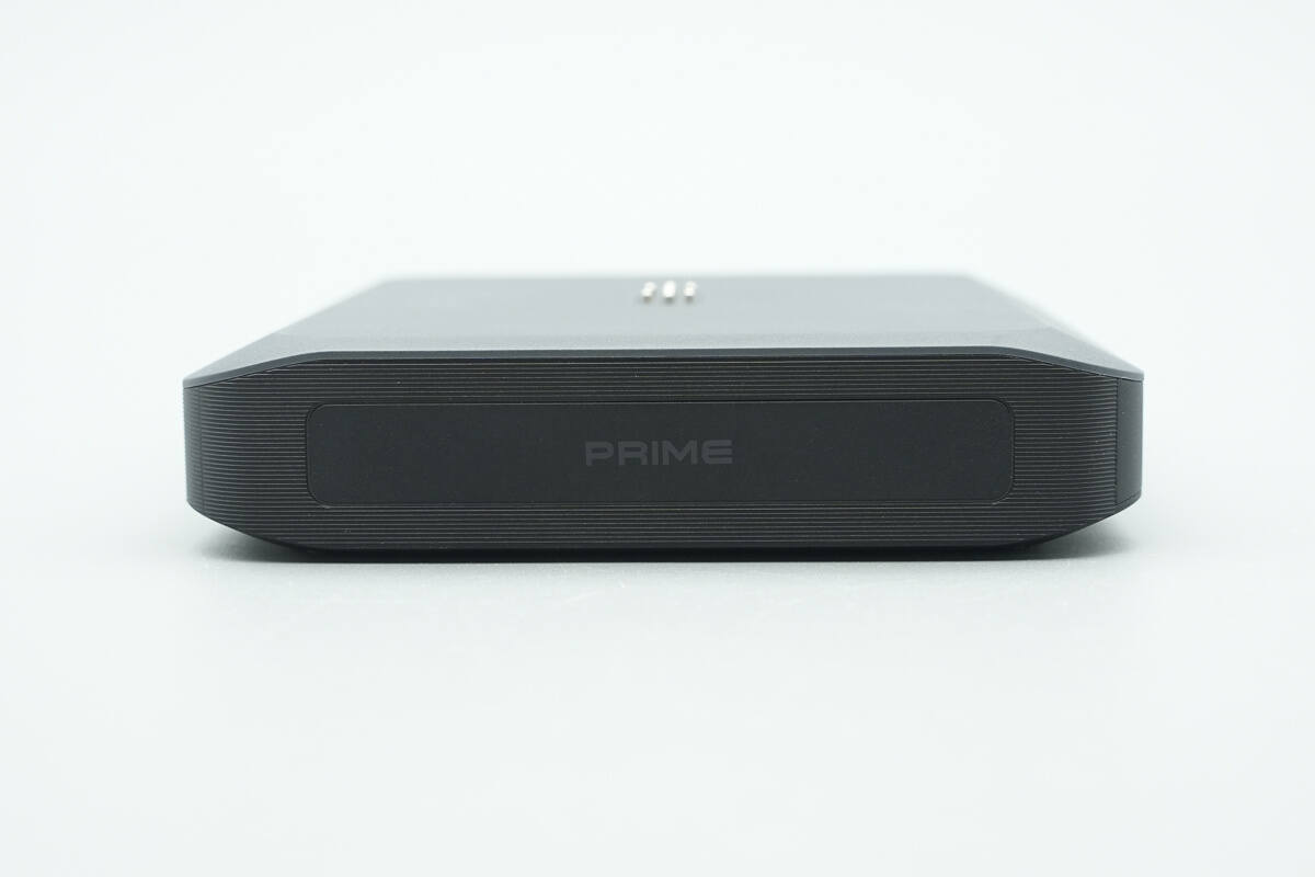
The other side panel is printed with the "PRIME".
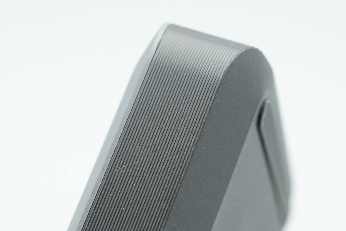
The side features a textured pattern, enhancing the grip and tactile feel.
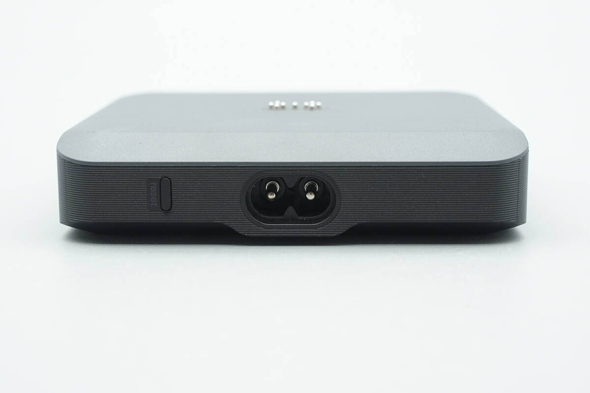
The rear features an 8-shaped power input port.
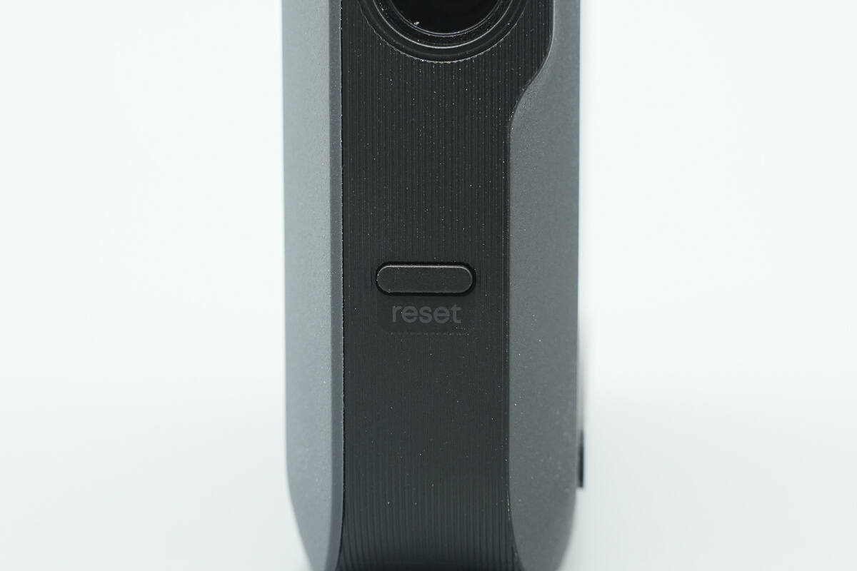
It is equipped with a reset button.
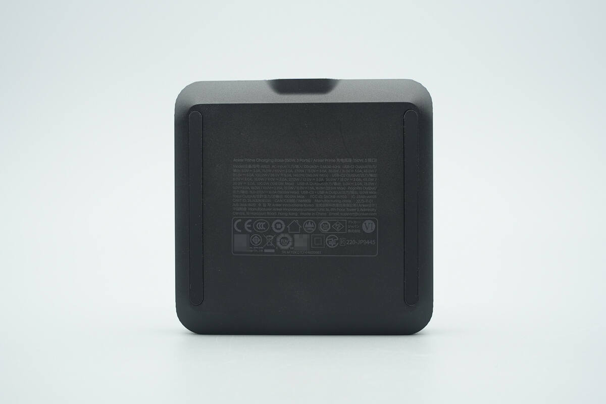
The bottom displays the technical specifications, and both sides are equipped with anti-slip pads.
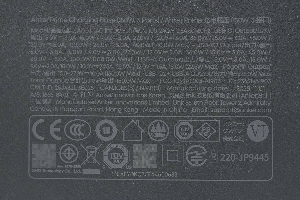
Model: A1903
Input: 100-240V~50/60Hz 2.5A
Output:
USB-C1: 5V3A, 9V3A, 12V3A, 15V3A, 20V5A, 28V5A 140W Max
USB-C2: 5V3A, 9V3A, 12V3A, 15V3A, 20V5A 100W Max
USB-A: 5V3A, 9V2A, 10V2.25A, 12V1.5A 22.5W Max
PogoPin: 15~27V10A (150.0W Max)
USB-C2 + USB-A: 15W Max
Total Output: 150W Max
The product is certified by CCC, CE, PSE, and also has VI-level energy efficiency certification.
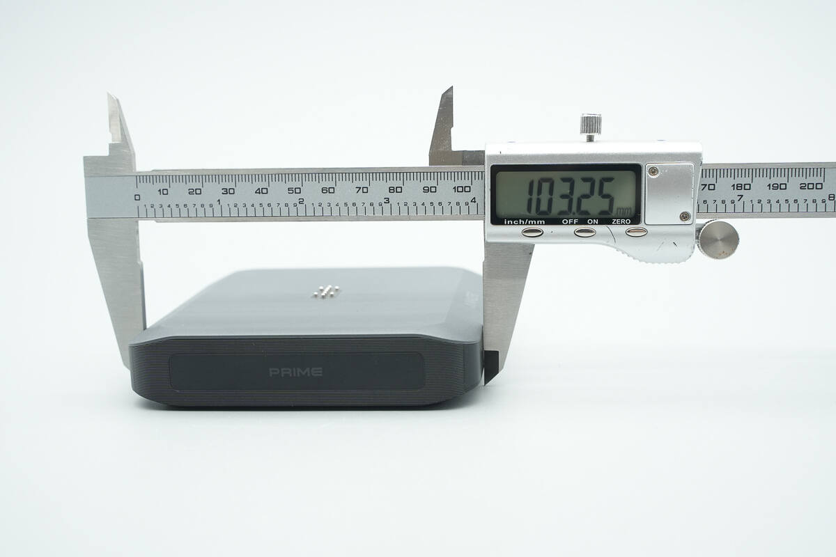
The length of the charging station is about 103.25 mm (4.065 inches).
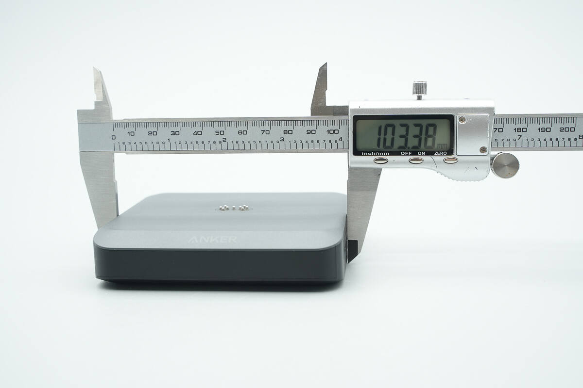
The width is about 103.38 mm (4.07 inches).
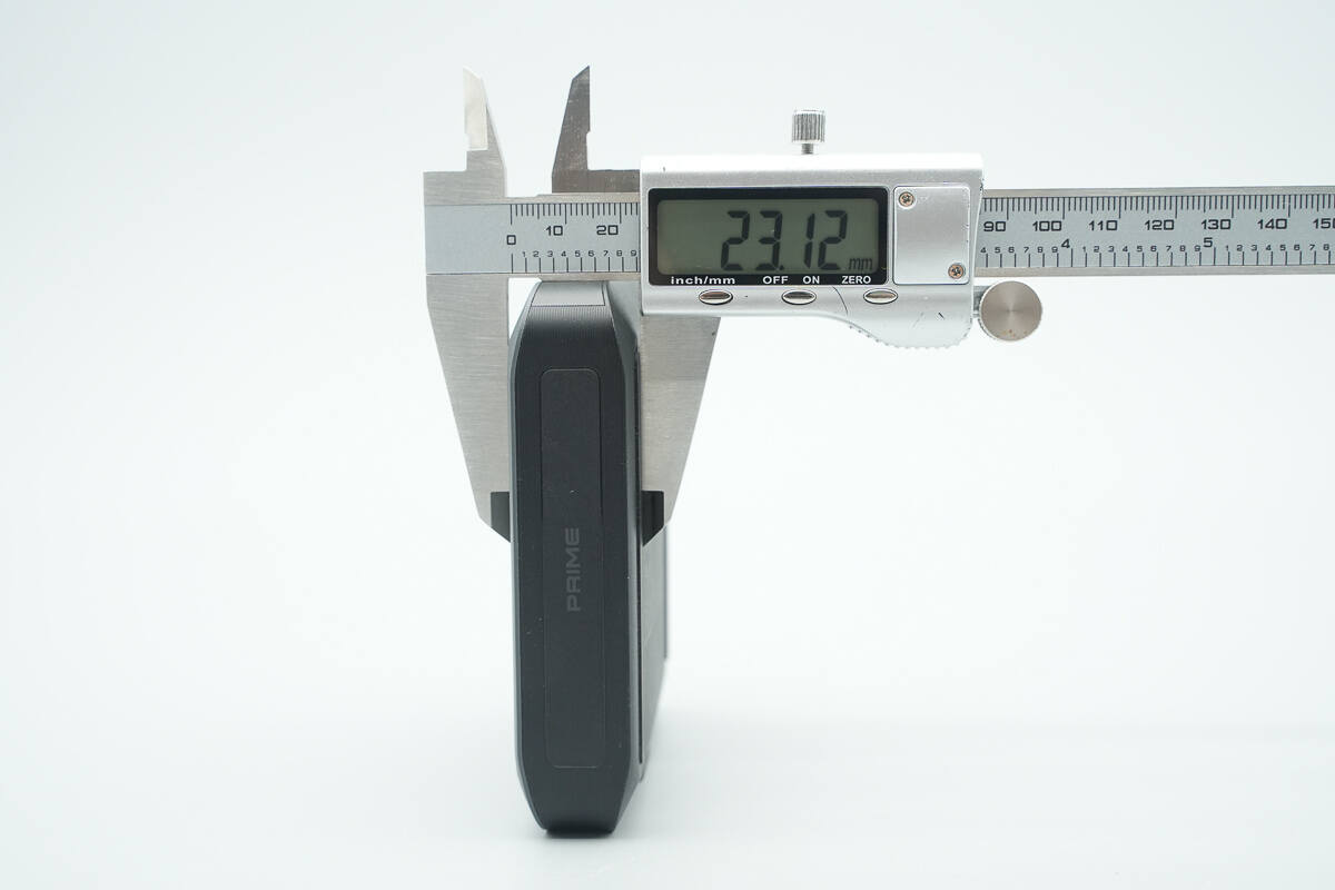
The thickness is about 23.12 mm (0.91 inches).
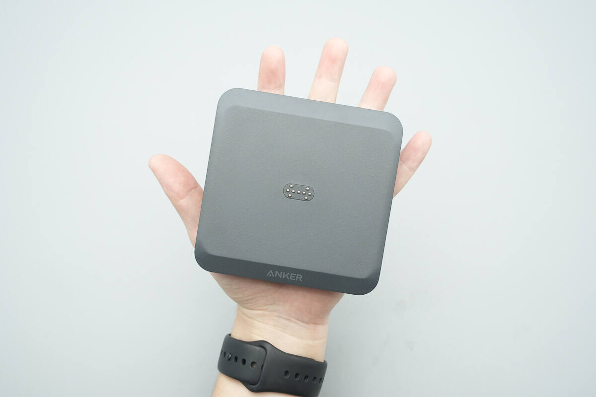
That's how big it is on the hand.
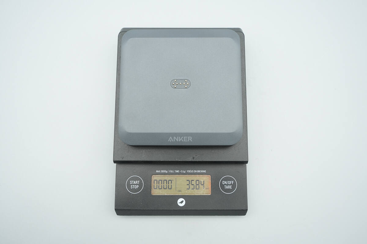
The weight is about 358 g (12.63 oz).
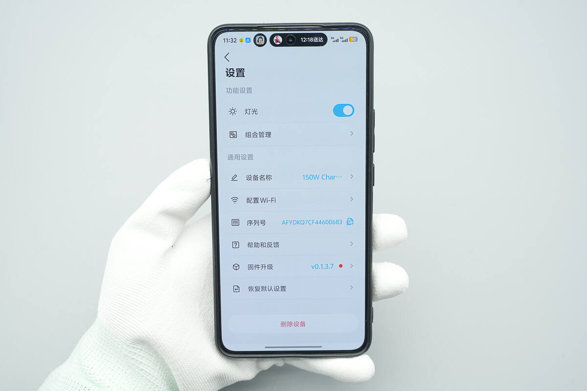
It supports Bluetooth connection with the app, allowing users to manage the charging dock’s name, lighting, Wi-Fi configuration, and more through the app. Additionally, it enables management of connected power banks.
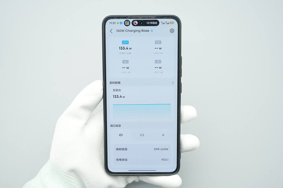
Through the app, users can also view the output data for each port, charging curves, and the total output power curve. It can also display information about the cables connected to each port and the used protocols.
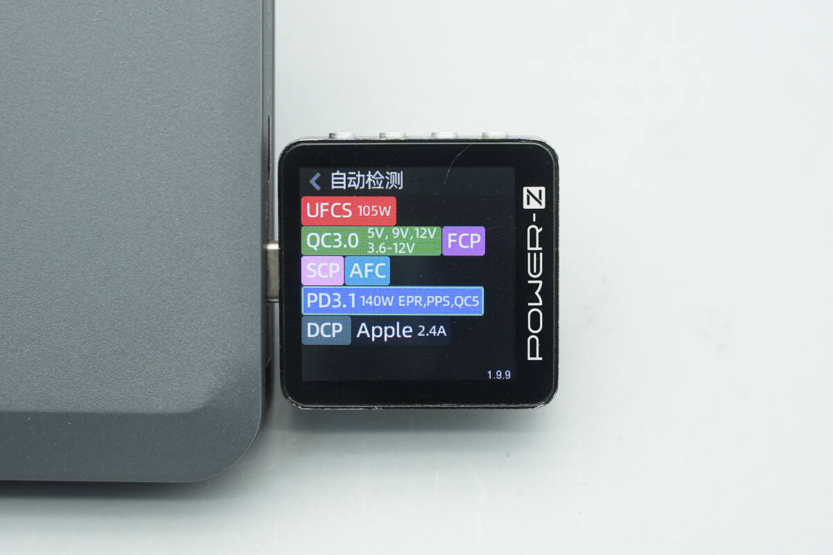
ChargerLAB POWER-Z KM003C shows that the USB-C1 supports QC3.0/5, FCP, SCP, AFC, PD3.1, PPS, DCP, and Apple 2.4A charging protocols.
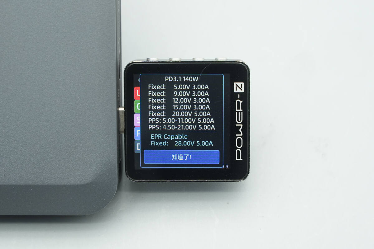
It has six fixed PDOs of 5V3A, 9V3A, 12V3A, 15V3A, 20V5A, and 28V5A, as well as two sets of PPS, which are 5-11V5A and 4.5-21V5A.
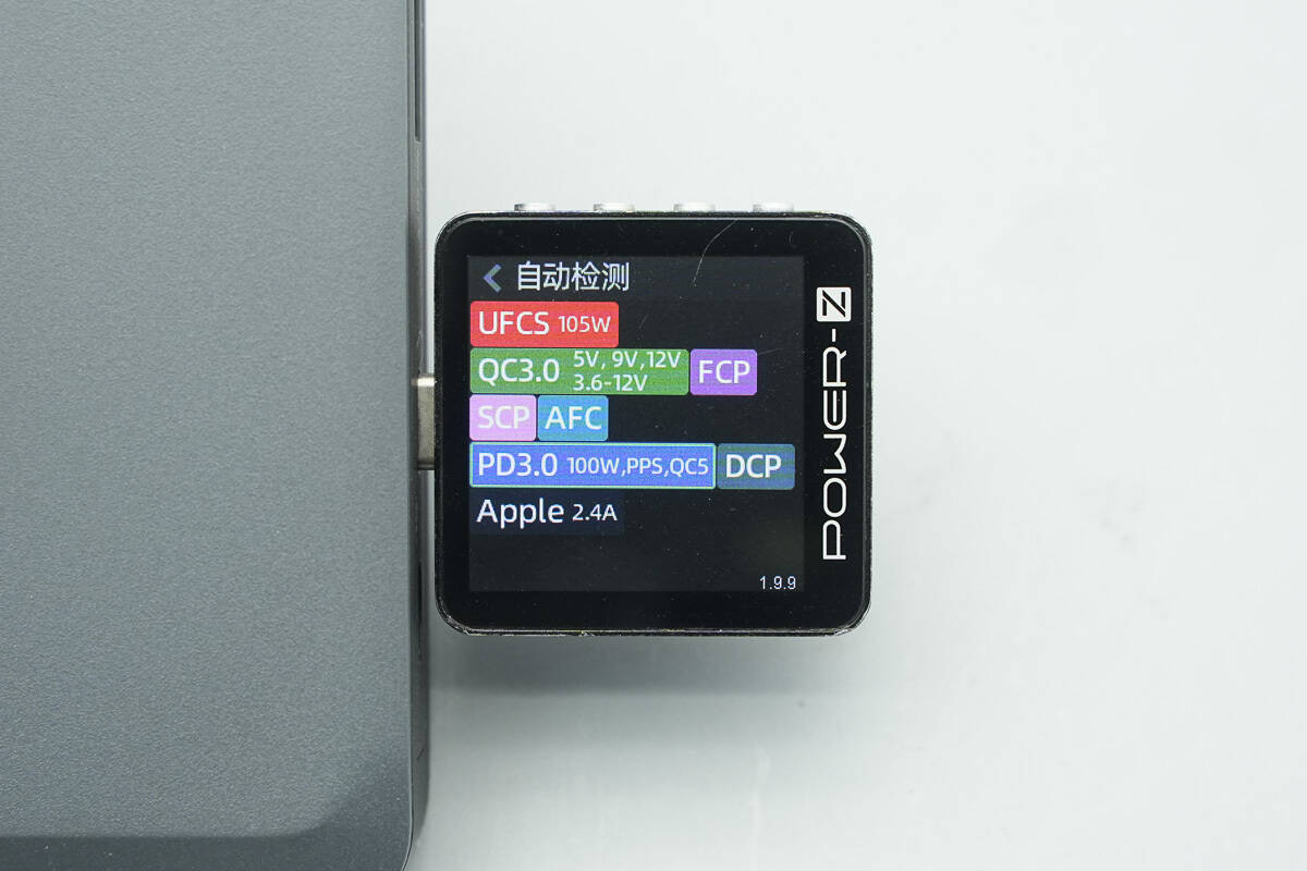
The USB-C2 supports QC3.0/5, FCP, SCP, AFC, PD3.0, PPS, DCP, and Apple 2.4A protocols.
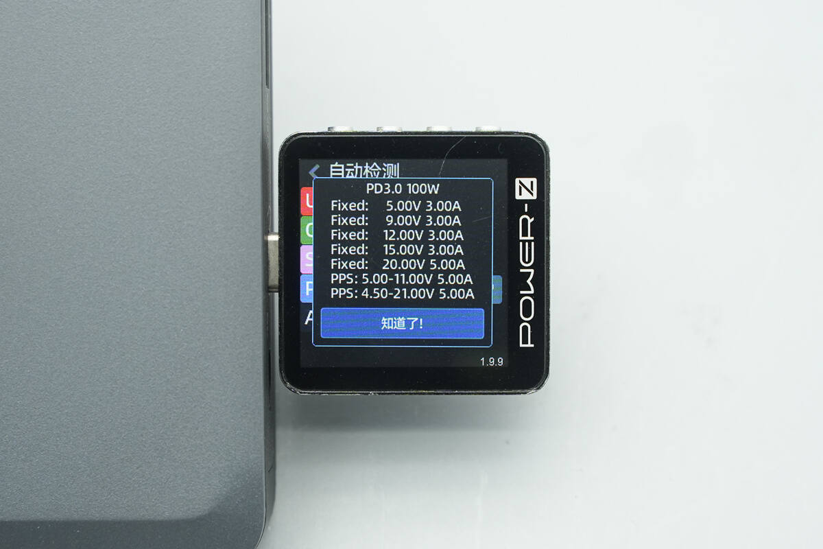
It has five fixed PDOs of 5V3A, 9V3A, 12V3A, 15V3A, and 20V5A, as well as two sets of PPS, which are 5-11V5A and 4.5-21V5A.
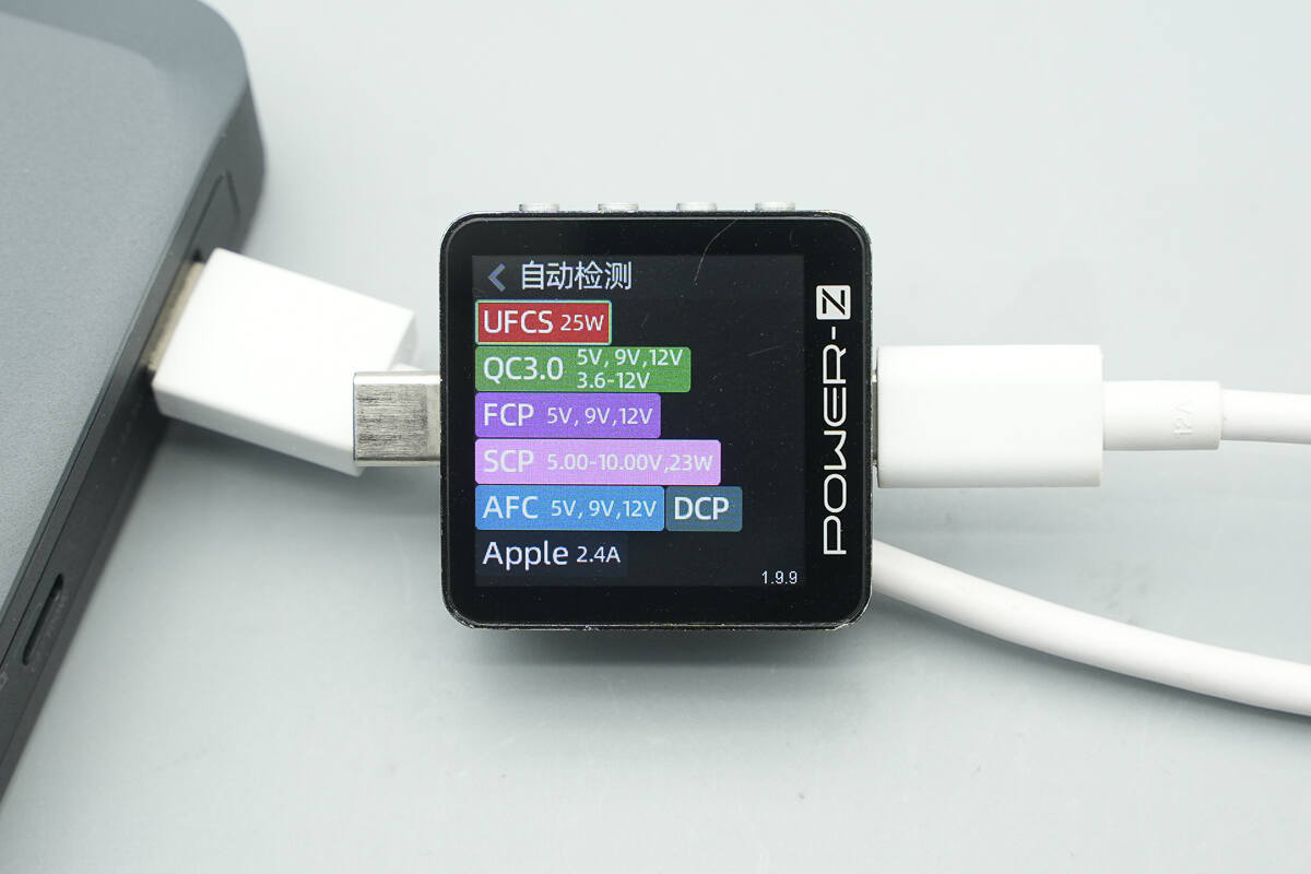
The USB-A supports QC3.0, FCP, SCP, AFC, DCP, and Apple 2.4A protocols.
Teardown
Next, let's take it apart to see its internal components and structure.
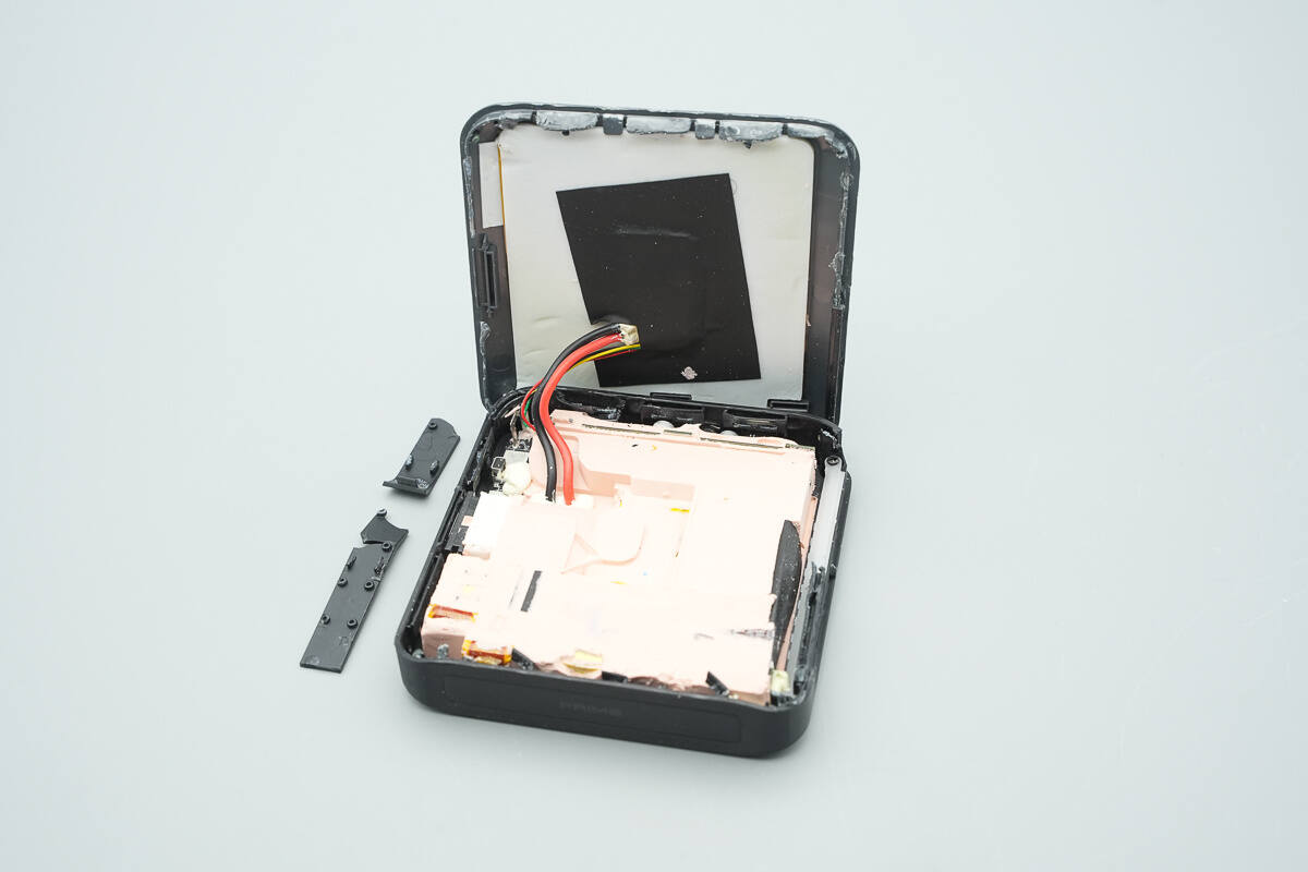
Open the top cover, which is secured with a snap-fit fastening system.
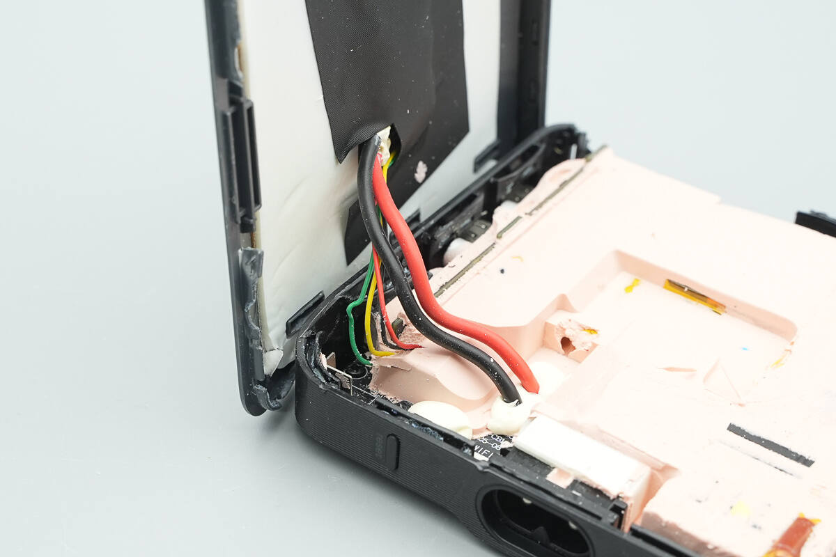
The Pogo Pin contacts on the PCB are connected to the PCBA module via two sets of wires.
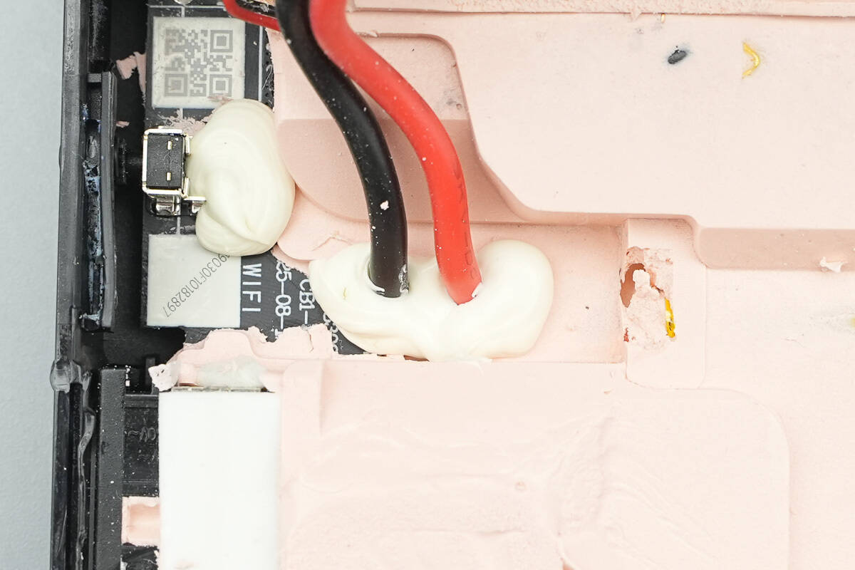
The soldering points of the thicker wires are coated with adhesive for reinforcement.
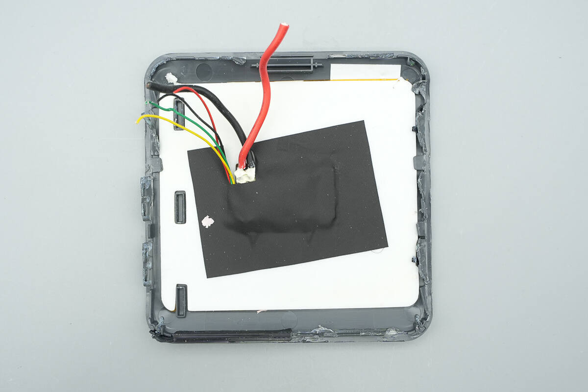
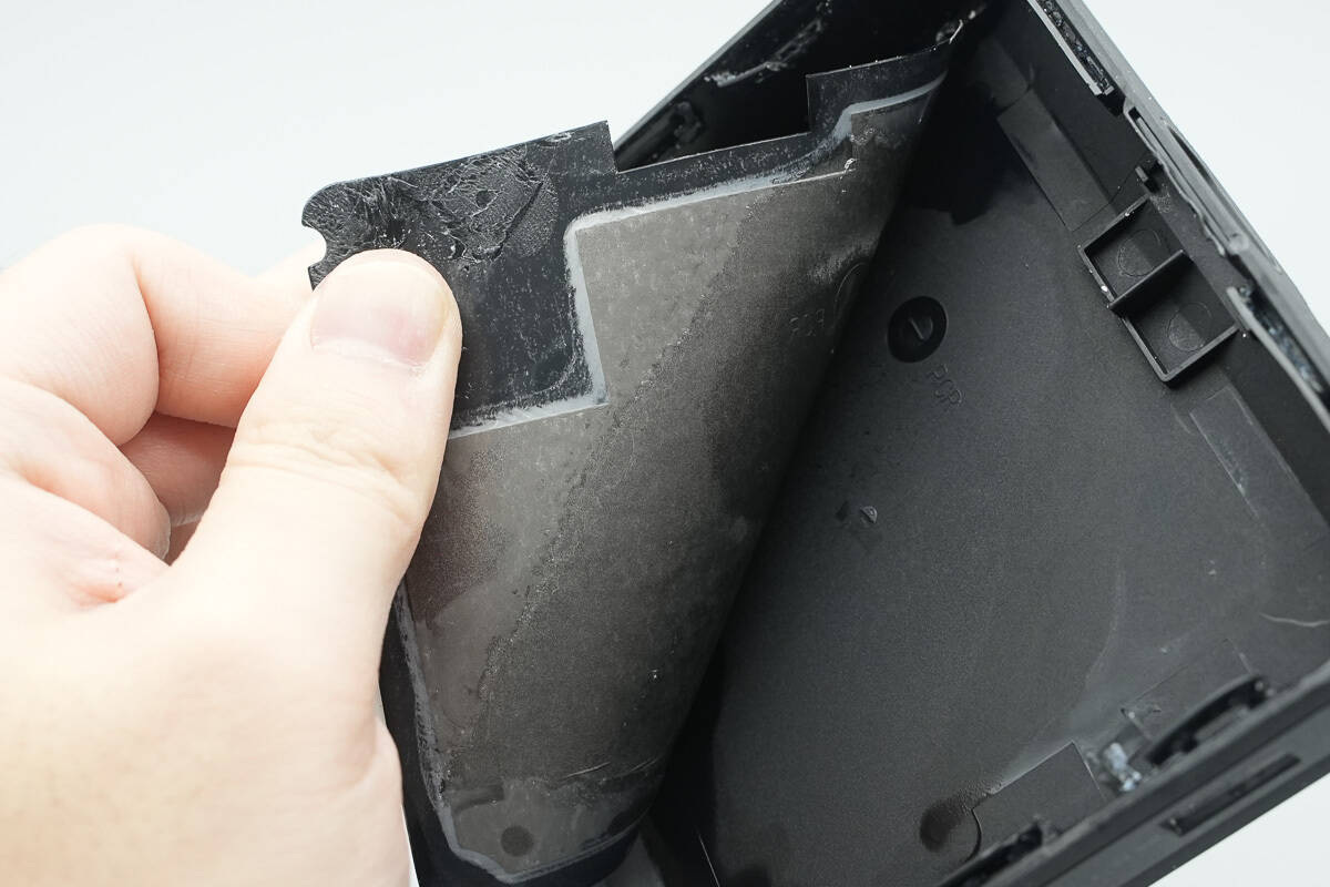
The inside of the cover plate is coated with a layer of aerogel.
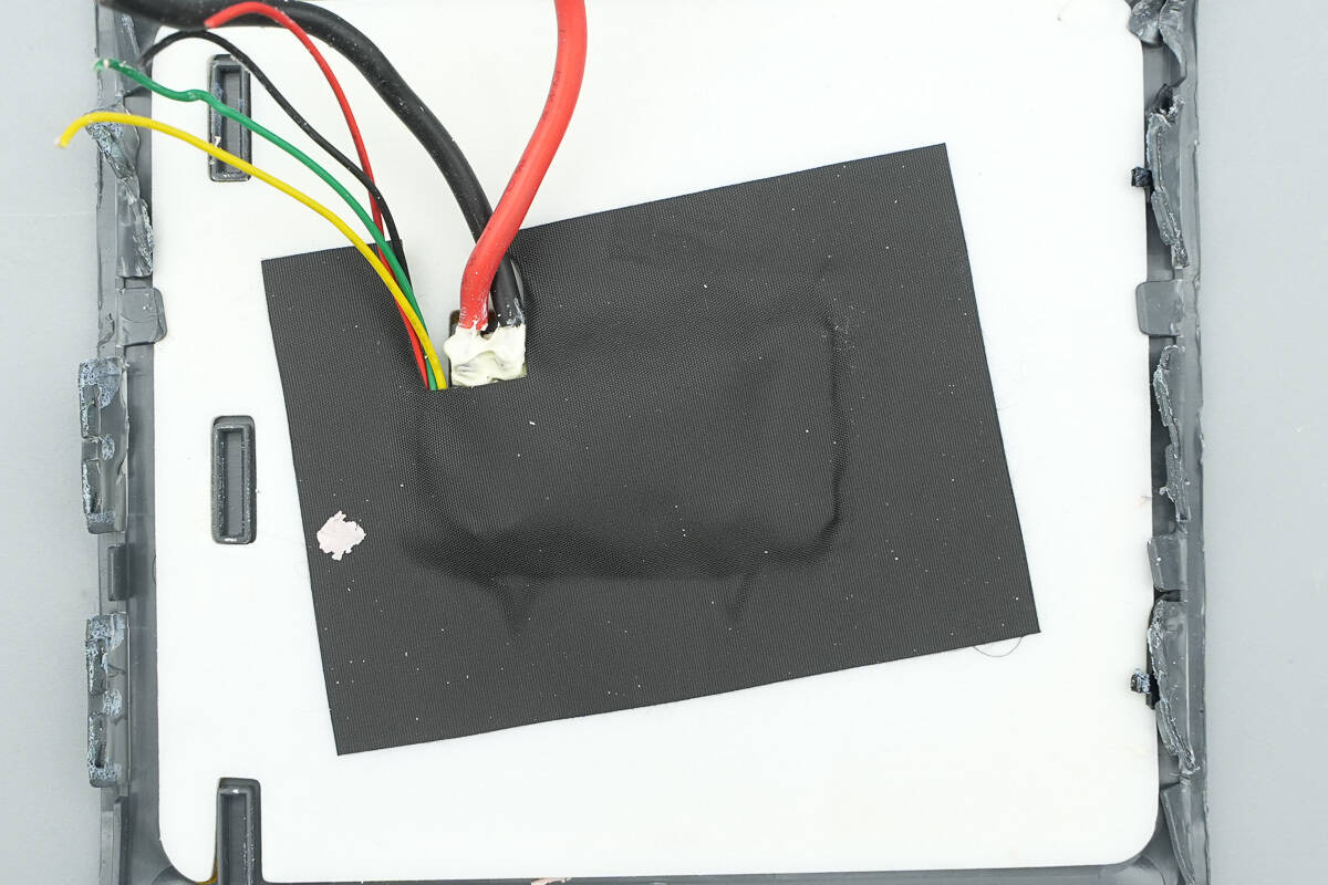
The area around the Pogo Pin contact PCB is covered with acetate cloth tape.
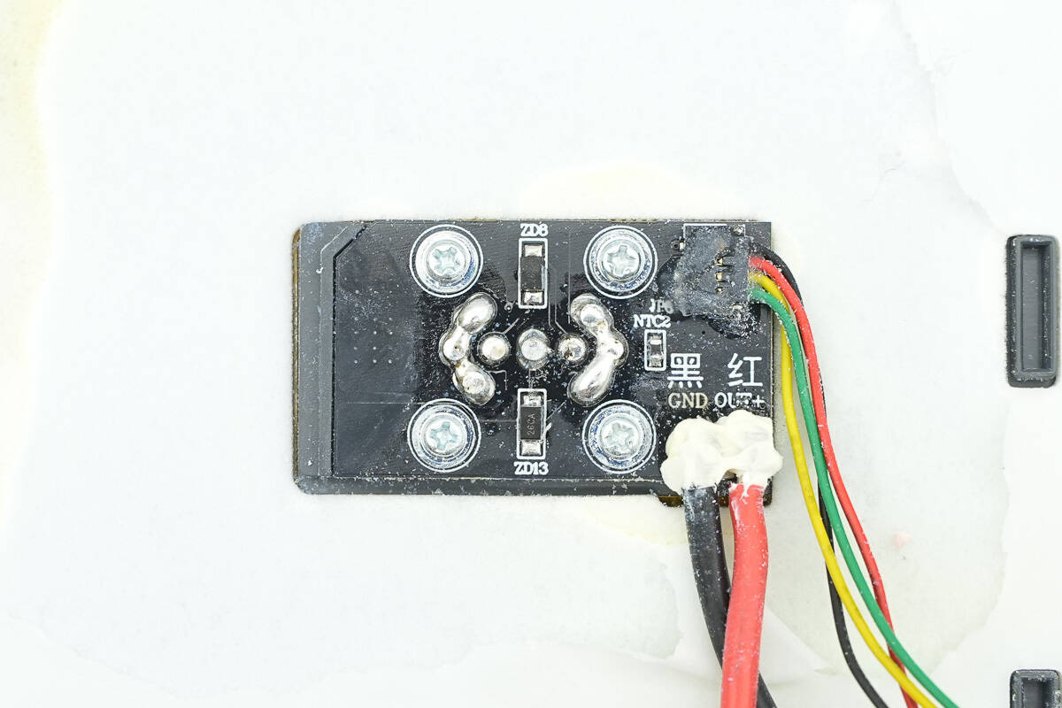
The PCB is secured in place using screws.
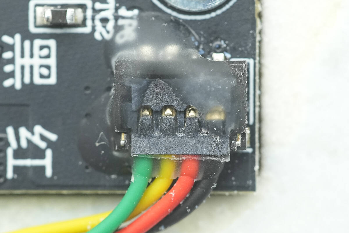
The other set of fine wires uses a plug-and-play connection, with the connection point reinforced by adhesive.

Both the PCBA module and the light guide strip are secured in place using screws.
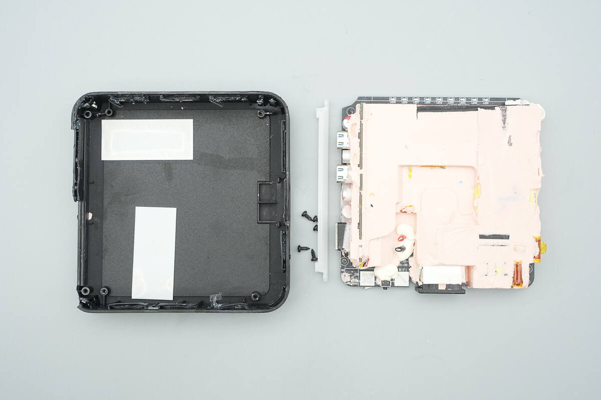
Remove the PCBA module and the light guide strip.
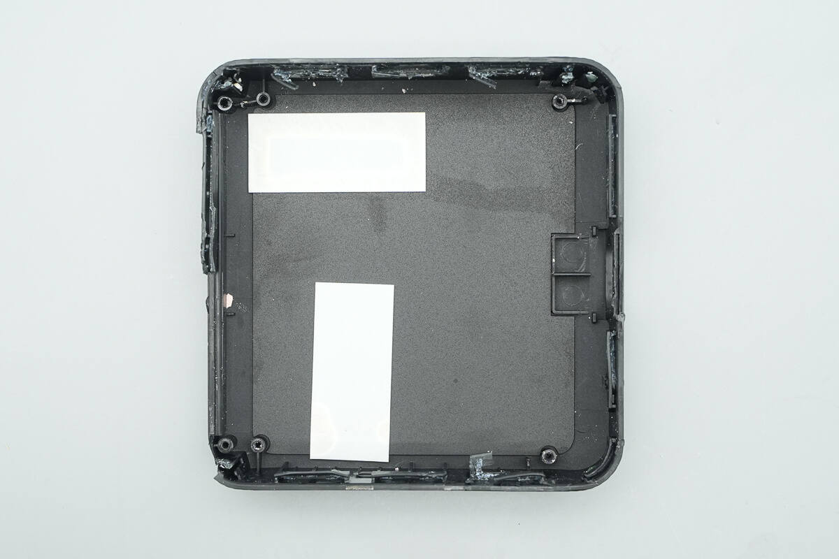
The inside of the other half of the outer shell is covered with Mylar film and aerogel pads.
The inside of the Mylar film is equipped with a graphite thermal pad for heat dissipation.
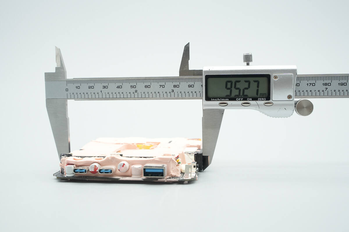
The length of the PCBA module is about 95.27 mm (3.75 inches).
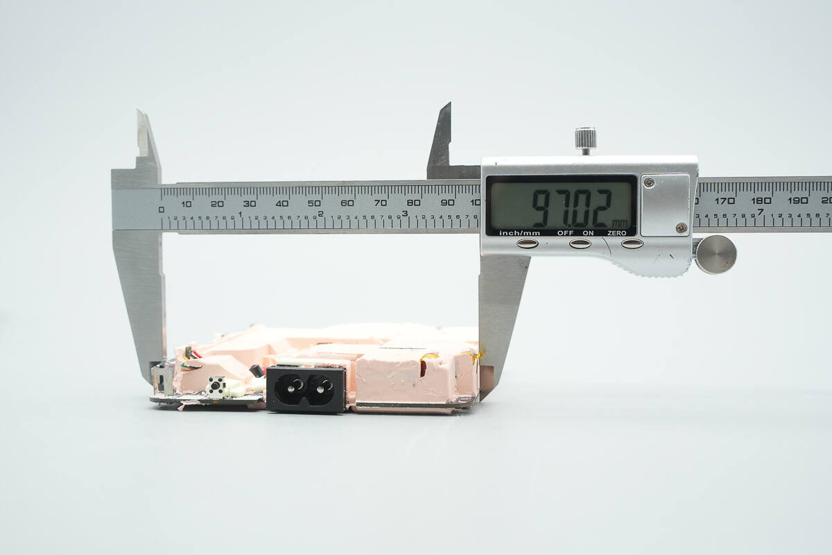
The width is about 97.02 mm (3.82 inches).
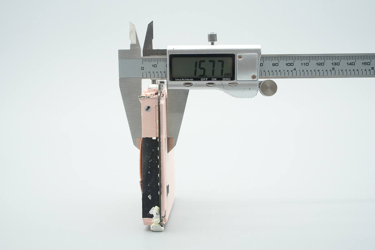
The thickness is about 15.77 mm (0.62 inches).
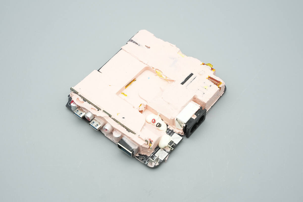
The PCBA module is covered with pink thermal gel, enhancing both heat dissipation and weather resistance.
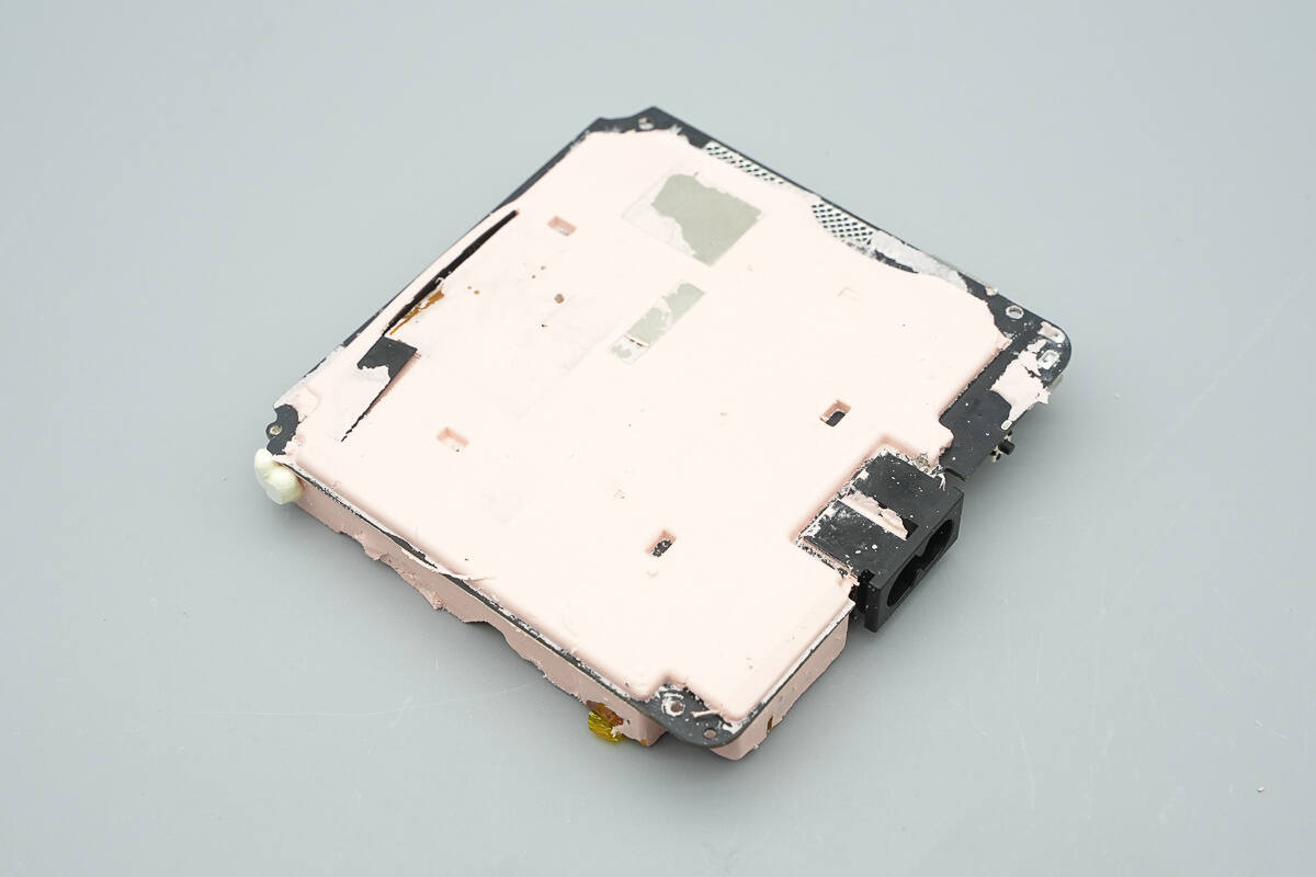
The back surface is also mostly covered with thermal adhesive.
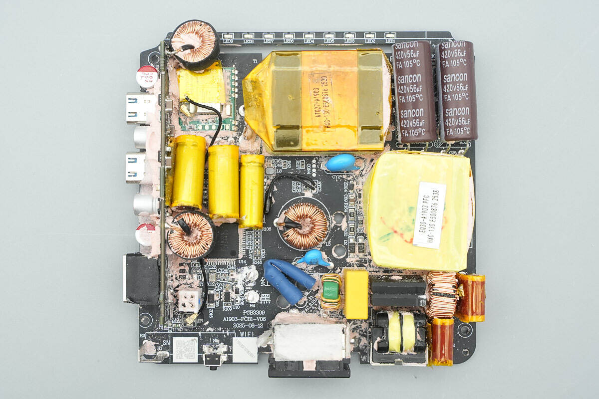
Remove the thermal adhesive. The right side of the front of the PCBA module is equipped with components such as common mode chokes, bridge rectifiers, film capacitors, a PFC boost inductor, and high-voltage filtering electrolytic capacitors. On the left side, there are components such as the output wireless communication module and the output PCB. On the left side, there are components such as the output wireless communication module and the output PCB.
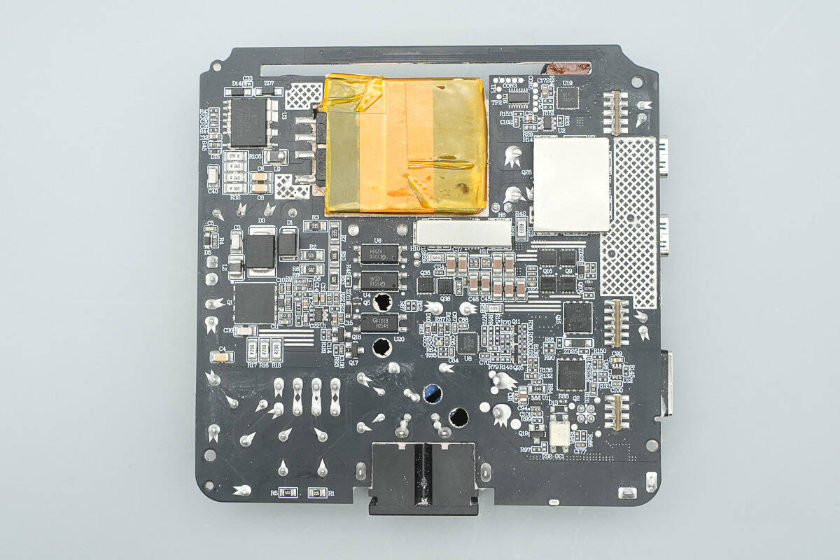
The back of the PCBA module features the PFC boost circuit, switch-mode power supply (SMPS) circuit, along with corresponding controllers, power devices, and other components. The transformer is soldered onto the board. The area where the synchronous rectifiers and PD controllers are located is equipped with dedicated heat sinks for improved thermal management.
The fuse is covered with a plastic insulating tube.
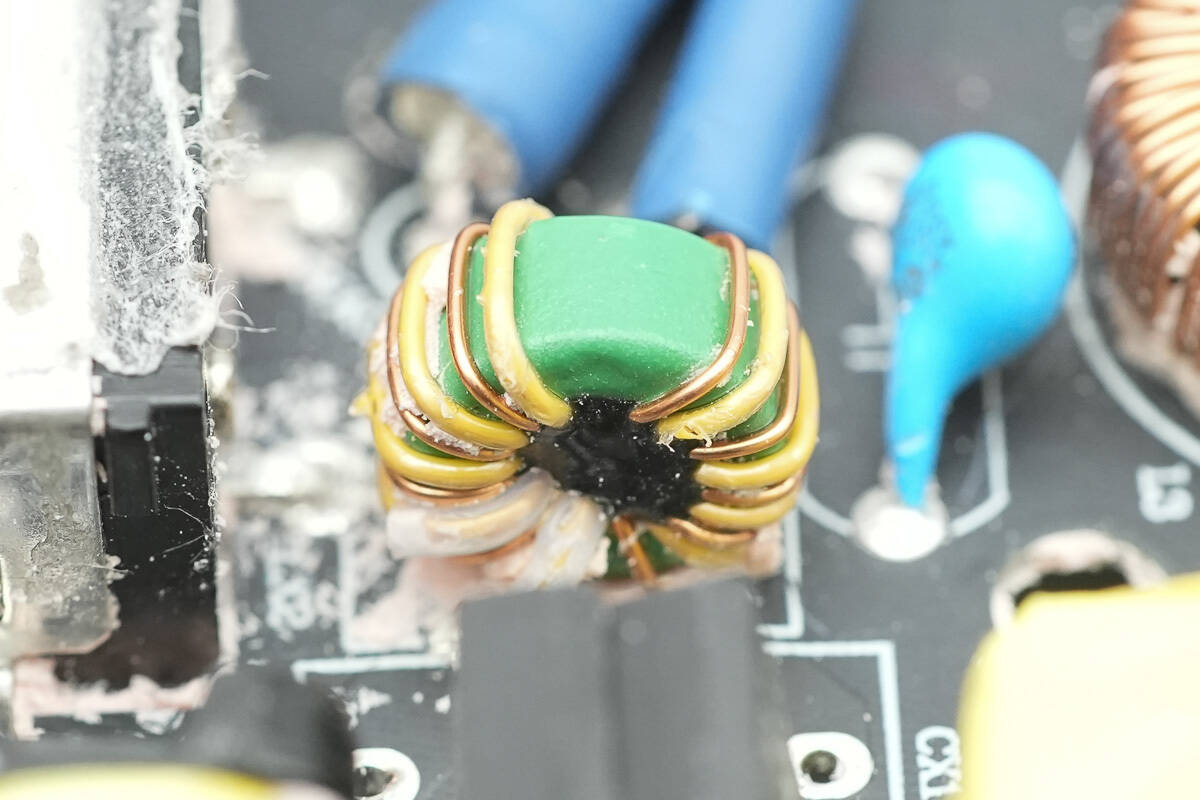
The common mode choke is used to filter out EMI.
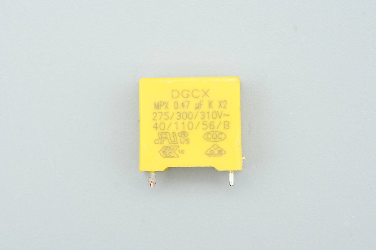
The safety X2 capacitor is from DGCX, with a capacitance of 0.47μF.
Close-up of the other common mode choke.
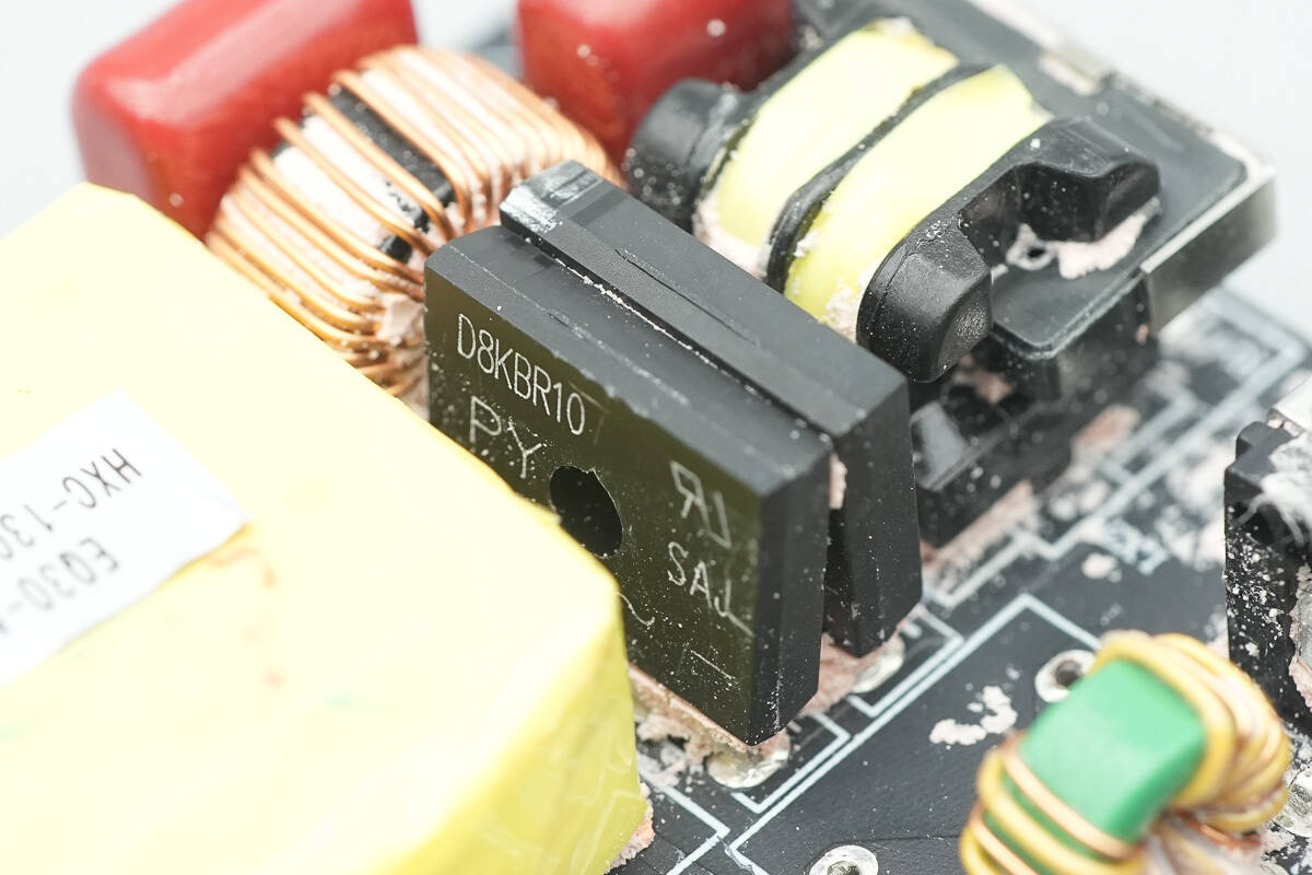
The two bridge rectifiers are from PY, model D8KBR10A, rated for 8A 1000V, and use a D3K package.
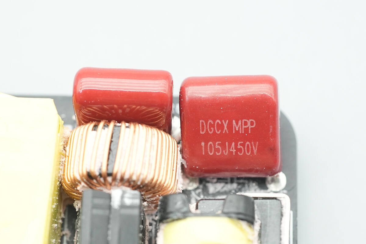
The two film capacitors are also from DGCX, each with a specification of 1μF 450V.
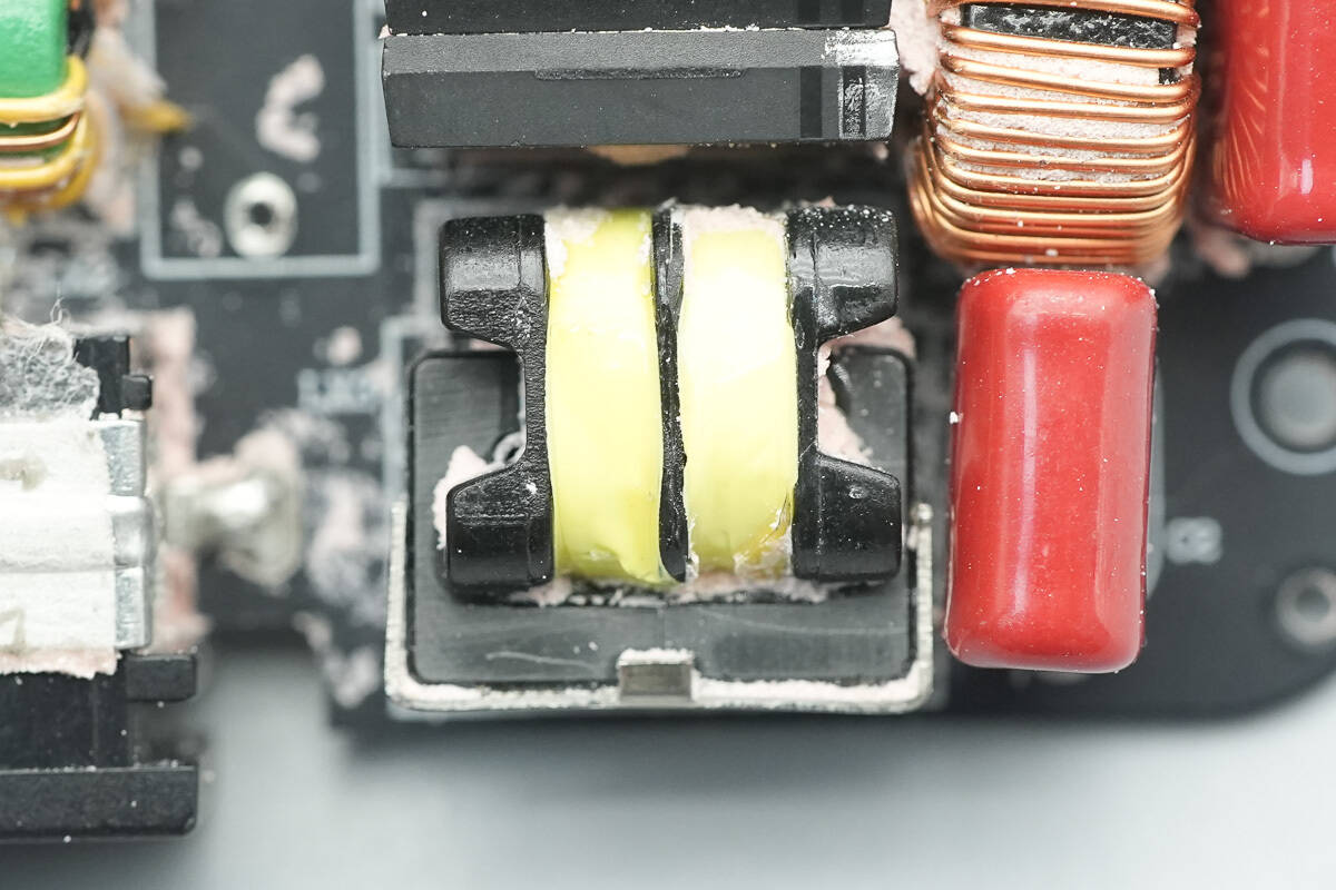
Close-up of the filter inductor.
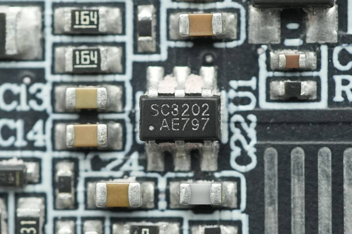
The SouthChip SC3202 is a high-efficiency boost PFC controller used in boost converters, employing a multi-mode control strategy. It operates in Critical Conduction Mode (CCM) under full or heavy load, and in Discontinuous Conduction Mode (DCM) when the load decreases, featuring valley-switching characteristics to lower switching frequency and improve efficiency.
In no-load conditions, the SC3202 operates in burst mode, reducing power consumption and minimizing audio noise. The SC3202 supports under-voltage protection, cycle-by-cycle over-current protection, output over-voltage protection, inductor current protection, and over-temperature protection. It comes in an SOT23-6 package and is suitable for applications like PD fast charging, adapters, and LED power supplies.
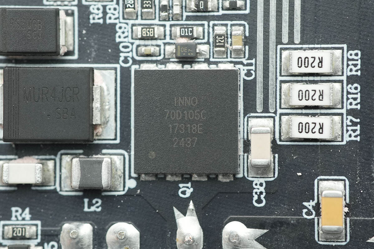
The PFC MOSFET is from Innoscience, model INN700D105C. This is an enhanced GaN single device with a 700V voltage rating and a R_DS(on) of 105mΩ. It supports ultra-high switching frequencies, has no reverse recovery charge, and features extremely low gate charge and output charge. The device meets JEDEC standards for industrial applications and includes built-in ESD protection. It complies with RoHS, is lead-free, and adheres to the EU REACH regulations. The INN700D105C is suitable for high-efficiency, high-density applications such as AC-DC conversion and DC-DC conversion. It comes in a DFN8x8 package.
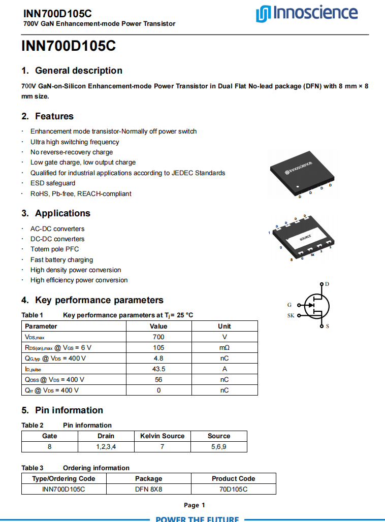
Here is the information about Innoscience INN700D105C.
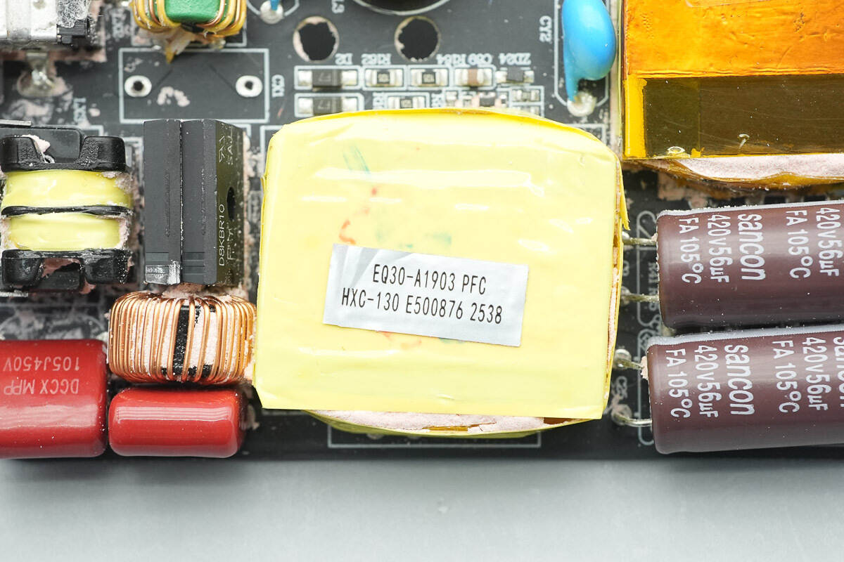
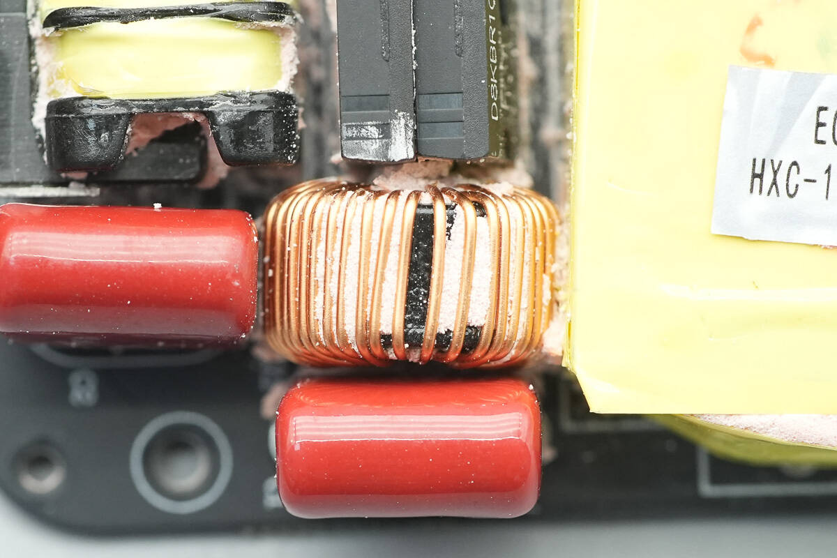
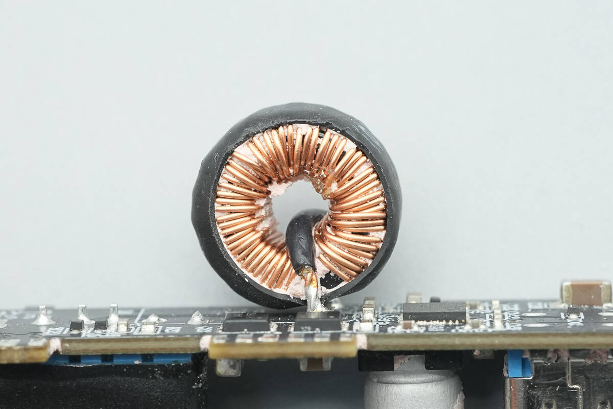
Close-up of the PFC boost inductor.
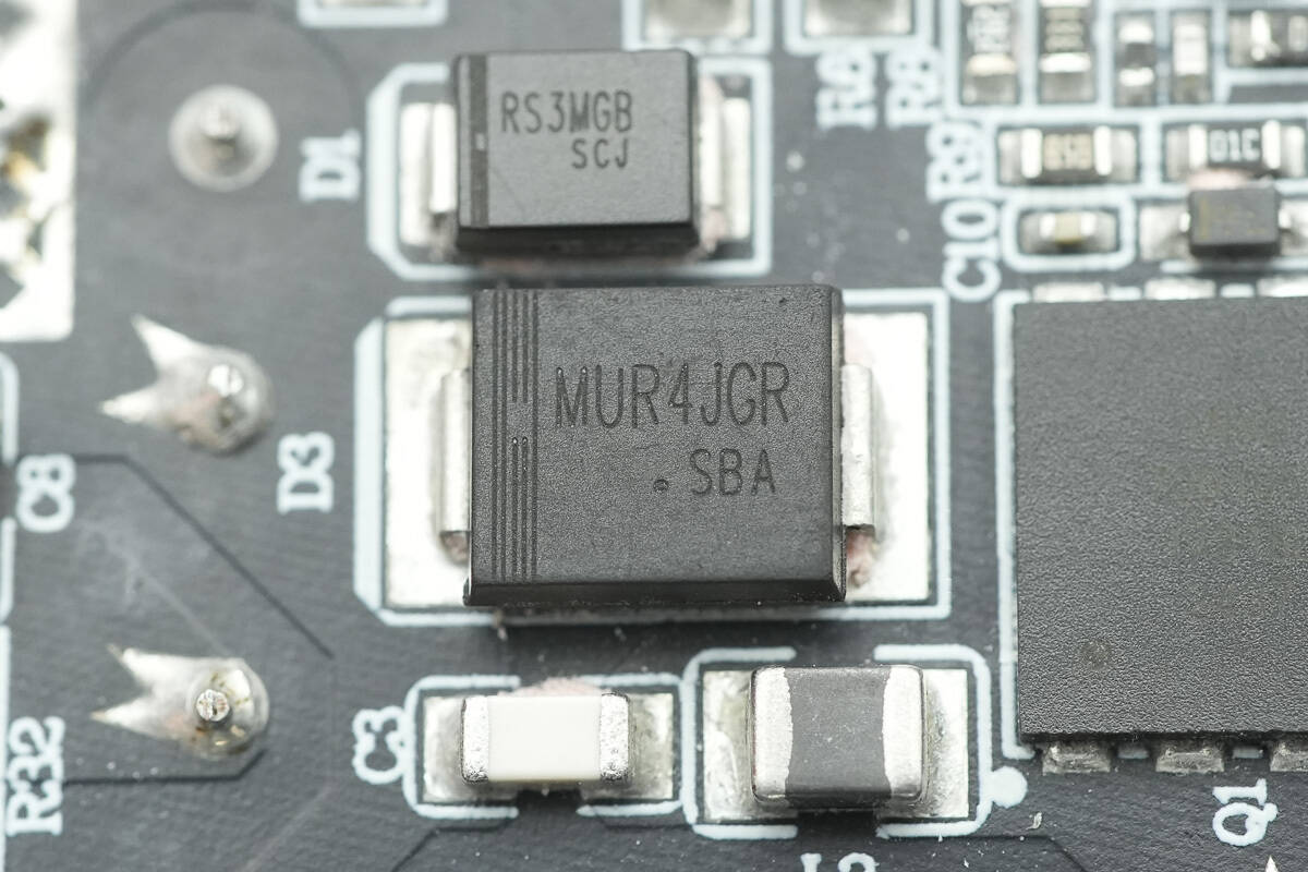
The PFC rectifier is marked with MUR4JGR, which is an ultra-fast recovery diode, featuring an SMC package.
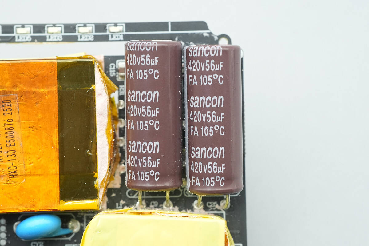
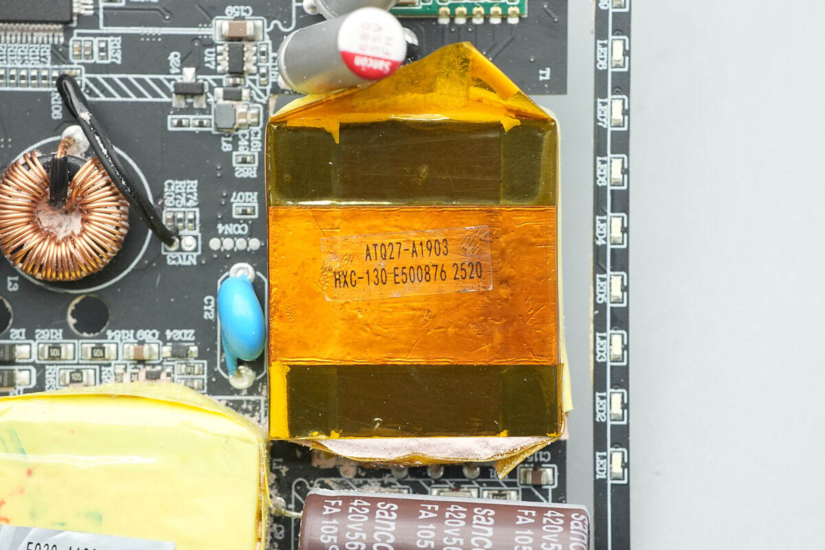
The two high-voltage filter electrolytic capacitors are from Sancon, each with a specification of 420V 56μF.
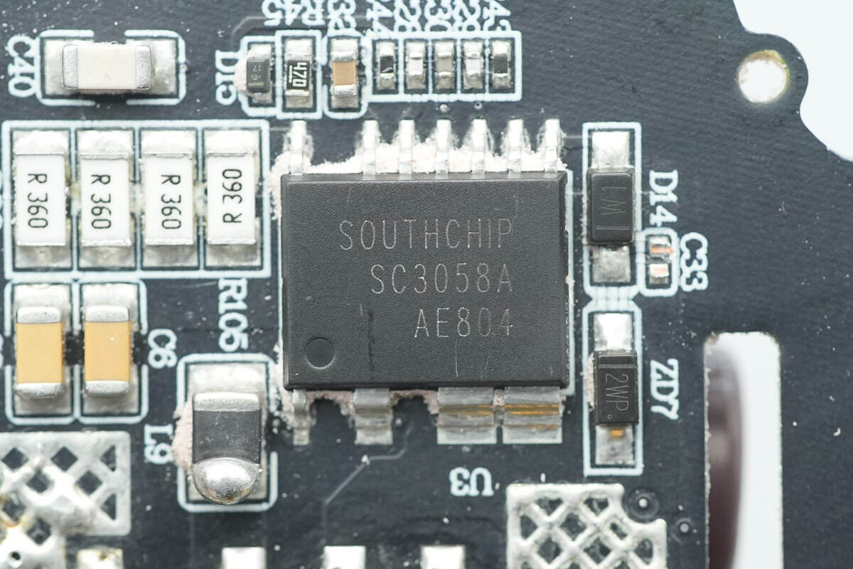
The integrated GaN chip is from SouthChip, model SC3058A, and it uses an ESOP10-W package.
Close-up of the transformer.
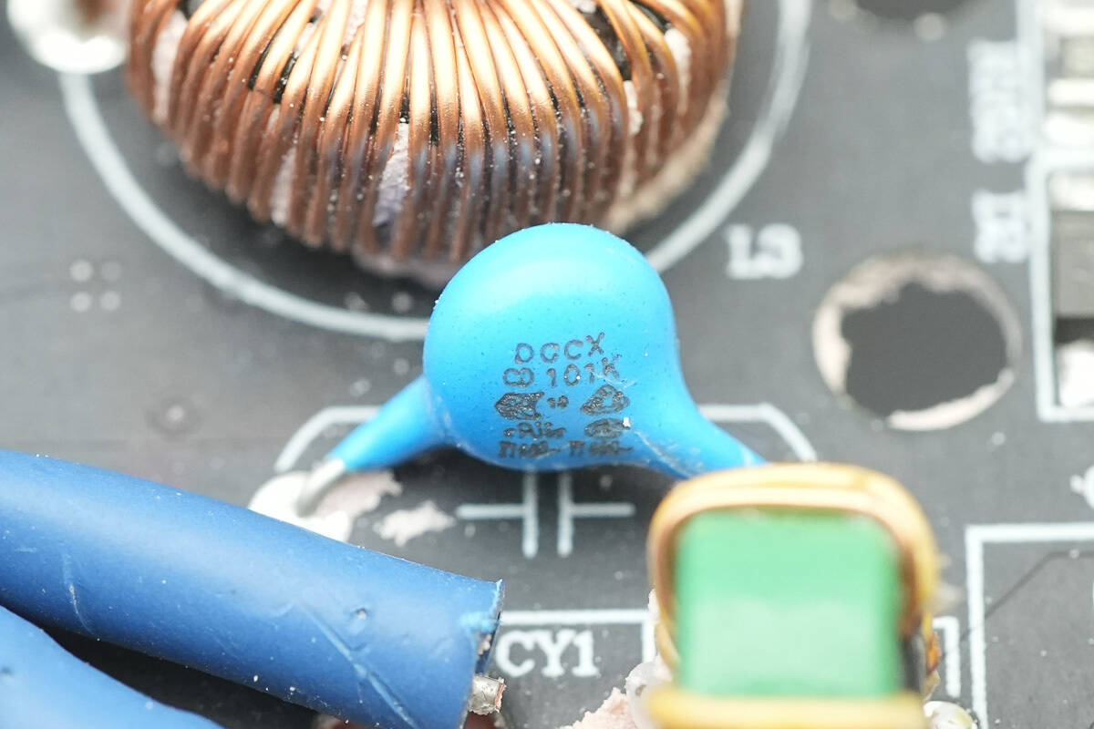
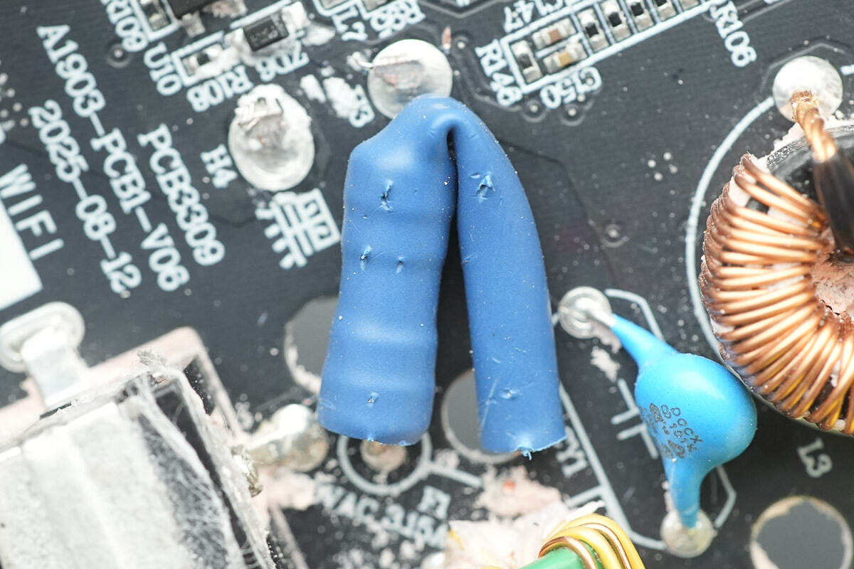
The blue Y capacitor is from DGCX.
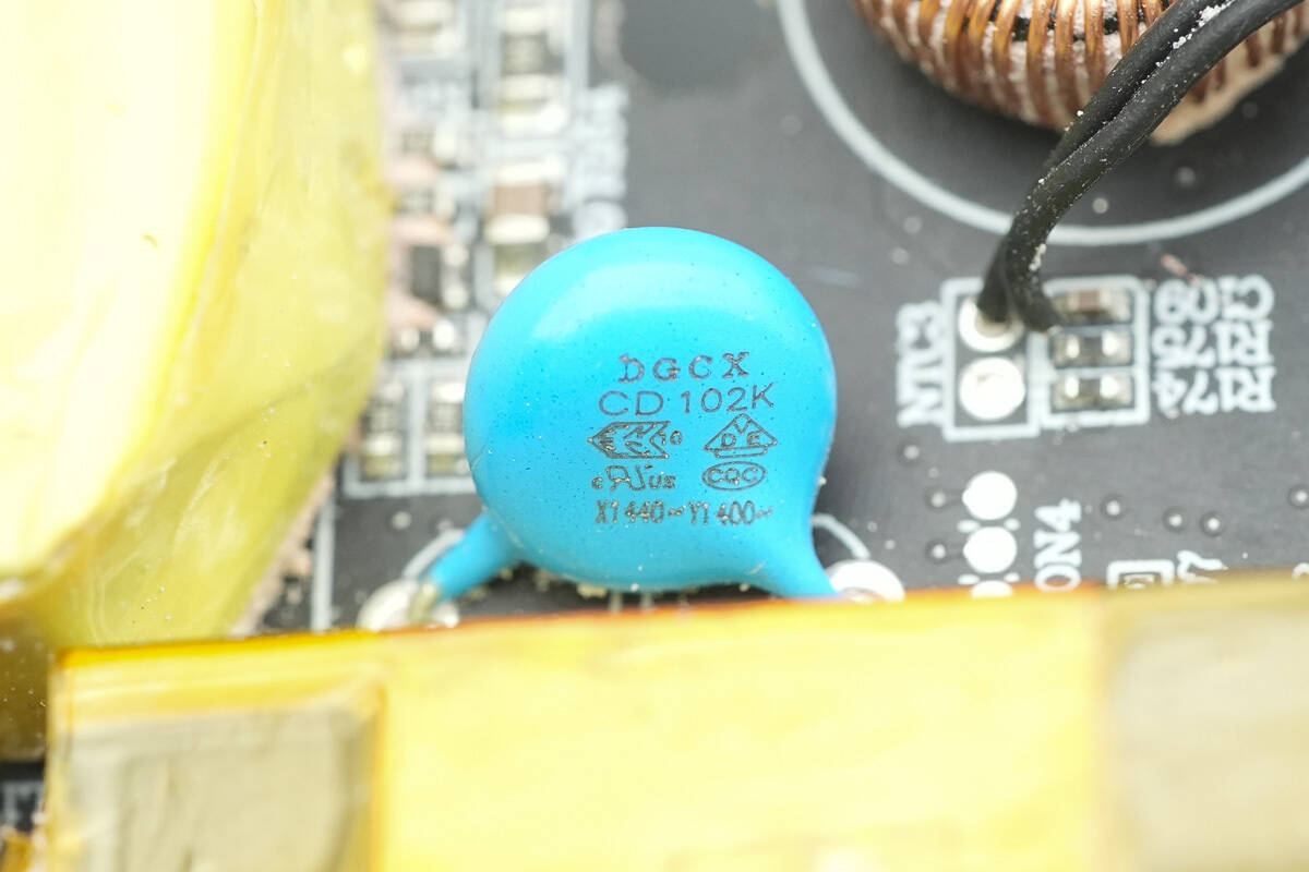
Close-up of the other Y capacitor.
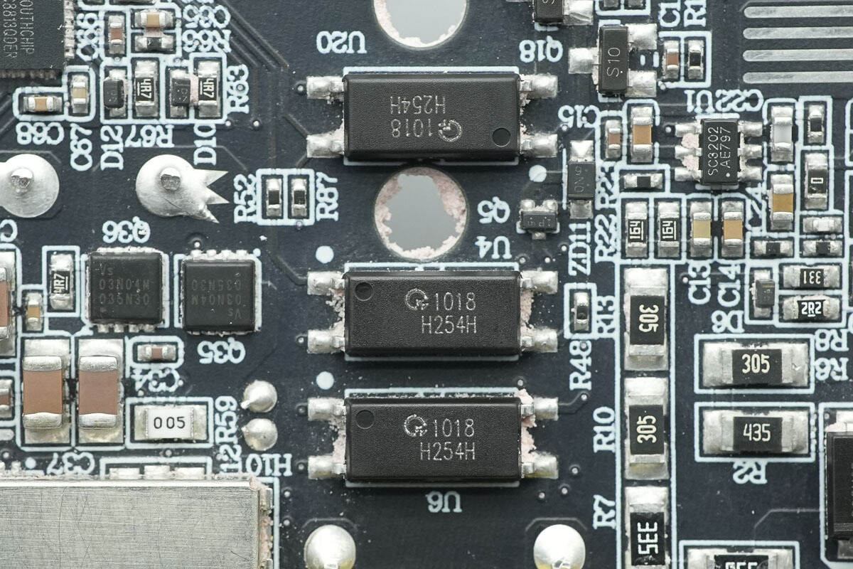
The optocouplers used for output voltage feedback and functional control are from Qunxin Microelectronics, marked with 1018 and part of the QX101X series. This optocoupler consists of a GaAs light-emitting diode and an NPN phototransistor.
The product features a current transfer ratio (CTR) of ≥50%, with an input-output isolation voltage of 5000Vrms. The collector-emitter breakdown voltage is ≥80V, and it operates within a temperature range of -55°C to 110°C. The QX101X series optocouplers are suitable for applications in switch-mode power supplies, smart meters, industrial control, instrumentation, office equipment, and home appliances.
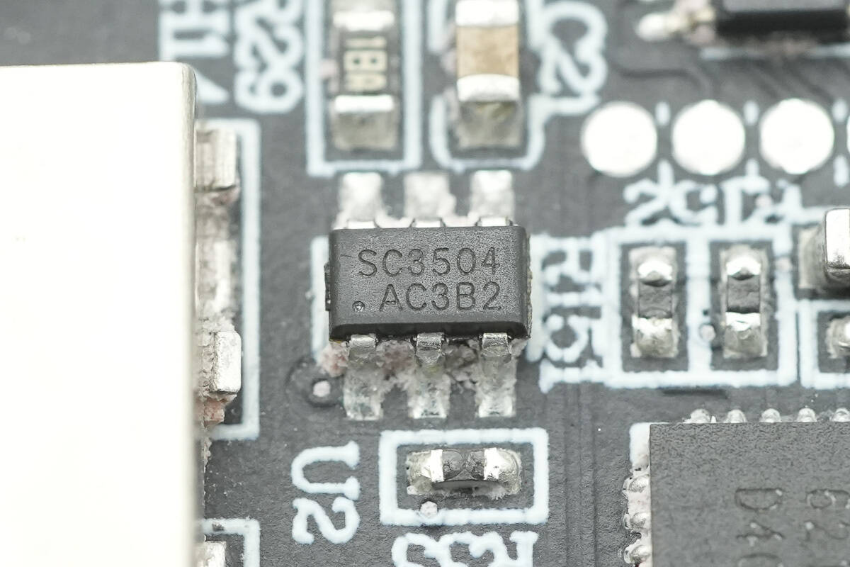
The synchronous rectifier controller is from SouthChip, model SC3504. It is specifically designed to drive the synchronous rectification N-channel power MOSFET in isolated flyback converters. This MOSFET can replace Schottky diodes, significantly improving system efficiency and optimizing thermal performance.
The SC3504 achieves precise control by continuously monitoring the drain-to-source voltage (VDS). When the VDS drops to the turn-on threshold, it activates the synchronous rectifier MOSFET. Once the VDS exceeds the turn-off threshold, it immediately turns off the MOSFET. The controller continuously monitors the conduction voltage drop of the synchronous rectifier to minimize conduction losses. Its ultra-fast turn-off comparator and drive circuit design ensure that the synchronous rectifier MOSFET operates safely even in Continuous Conduction Mode (CCM).
The SC3504 supports a wide output voltage range, making it an ideal choice for applications such as adapters, chargers, and USB power delivery (USB-PD). With its broad VDD operating range and advanced gate drive technology, the SC3504 is well-suited for applications that require flexible output voltage configurations. It also supports both high-side and low-side rectification configurations.
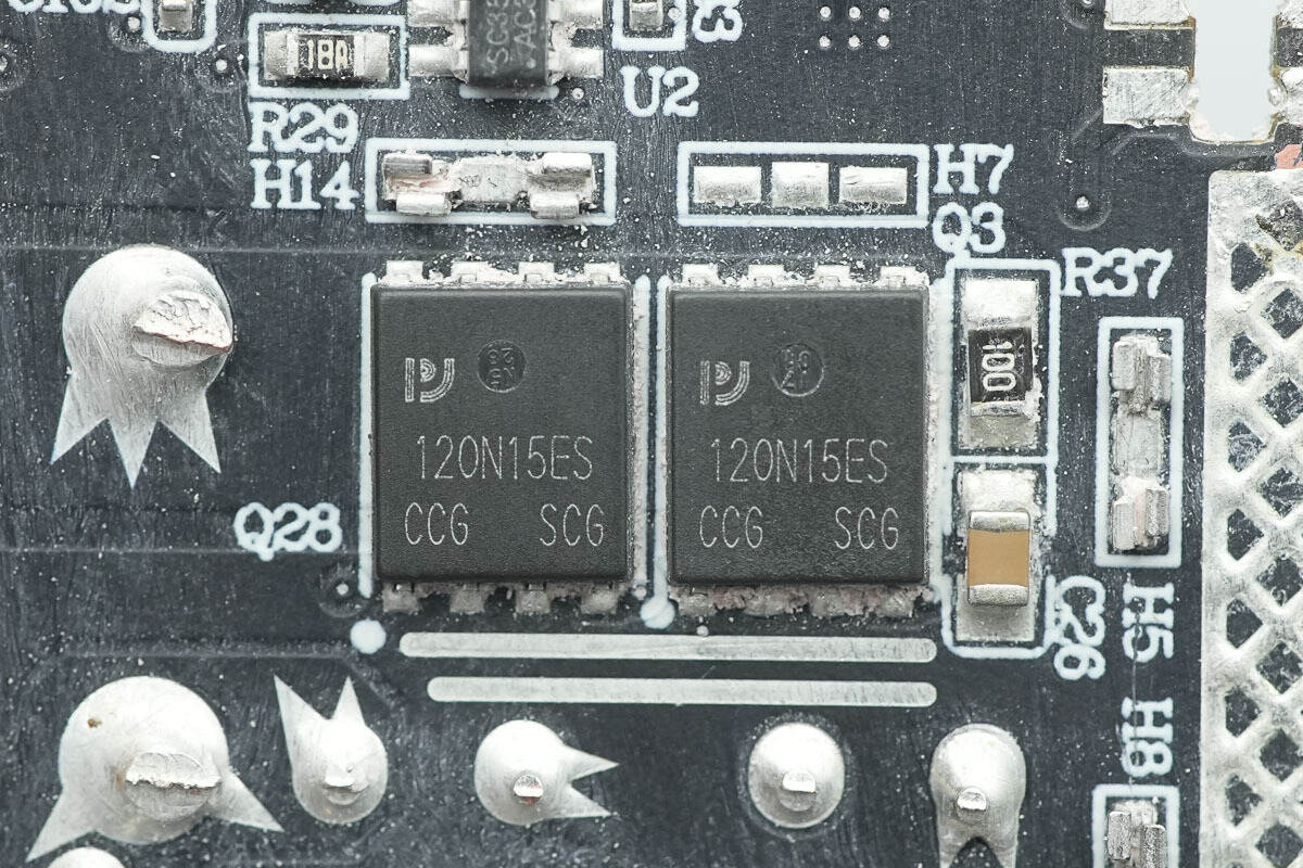
The synchronous rectifiers are from PY, model PW120N15ES, an NMOS with a voltage rating of 150V and a R_DS(on) of 9.3mΩ. They come in a DFN 5x6 package.
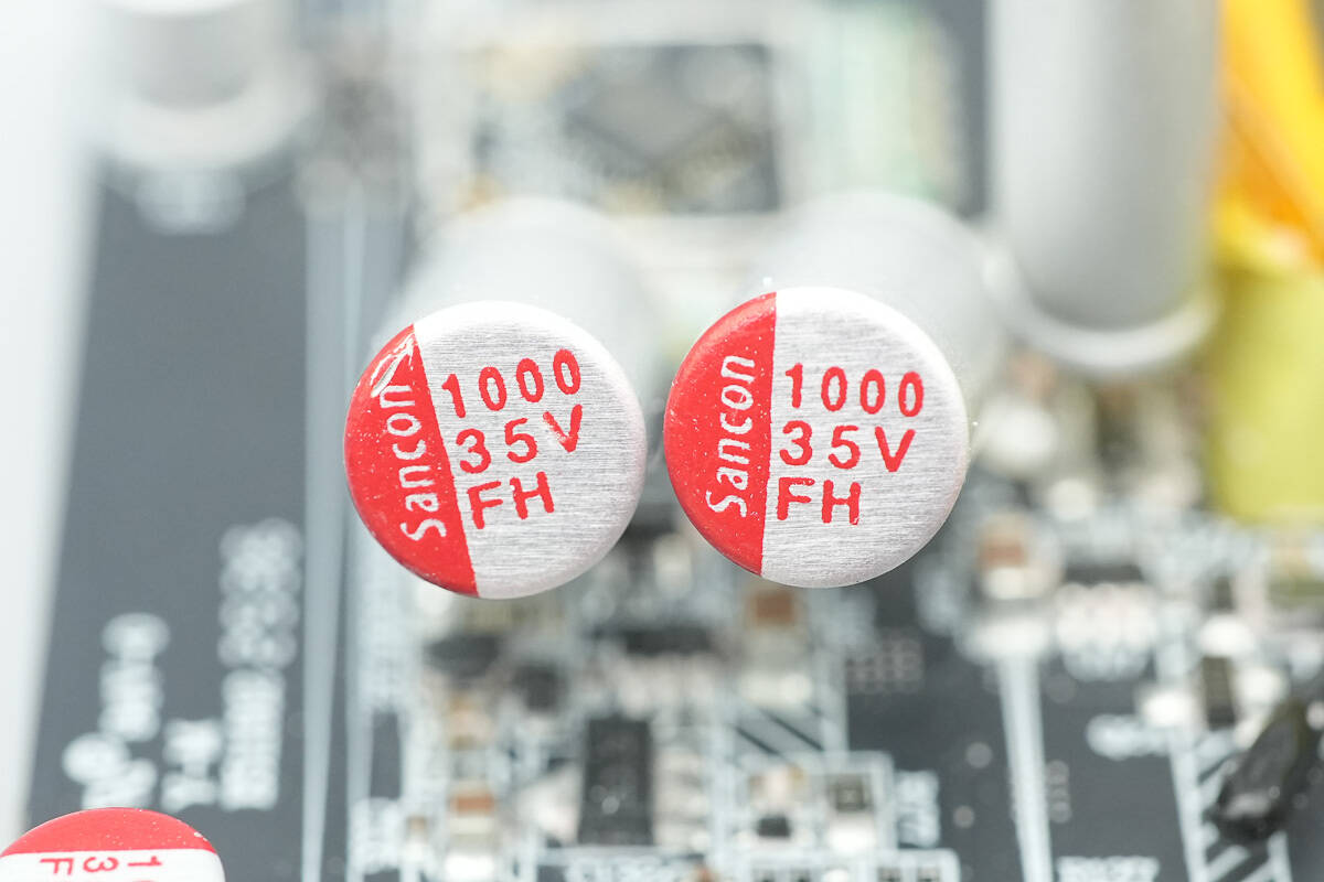
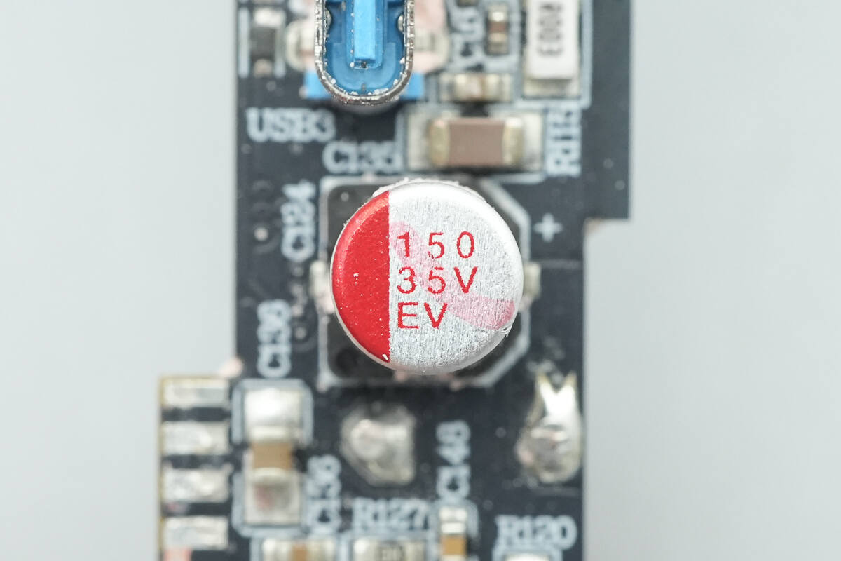
The solid capacitors used for output filtering are also from Sancon, with two capacitors each rated at 35V 1000μF.
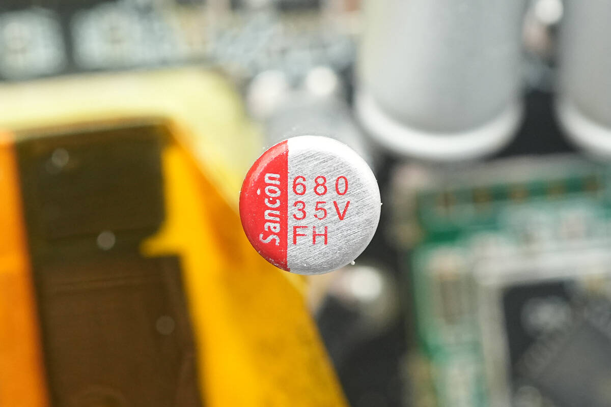
The third capacitor is also from Sancon, with a specification of 35V 680μF.
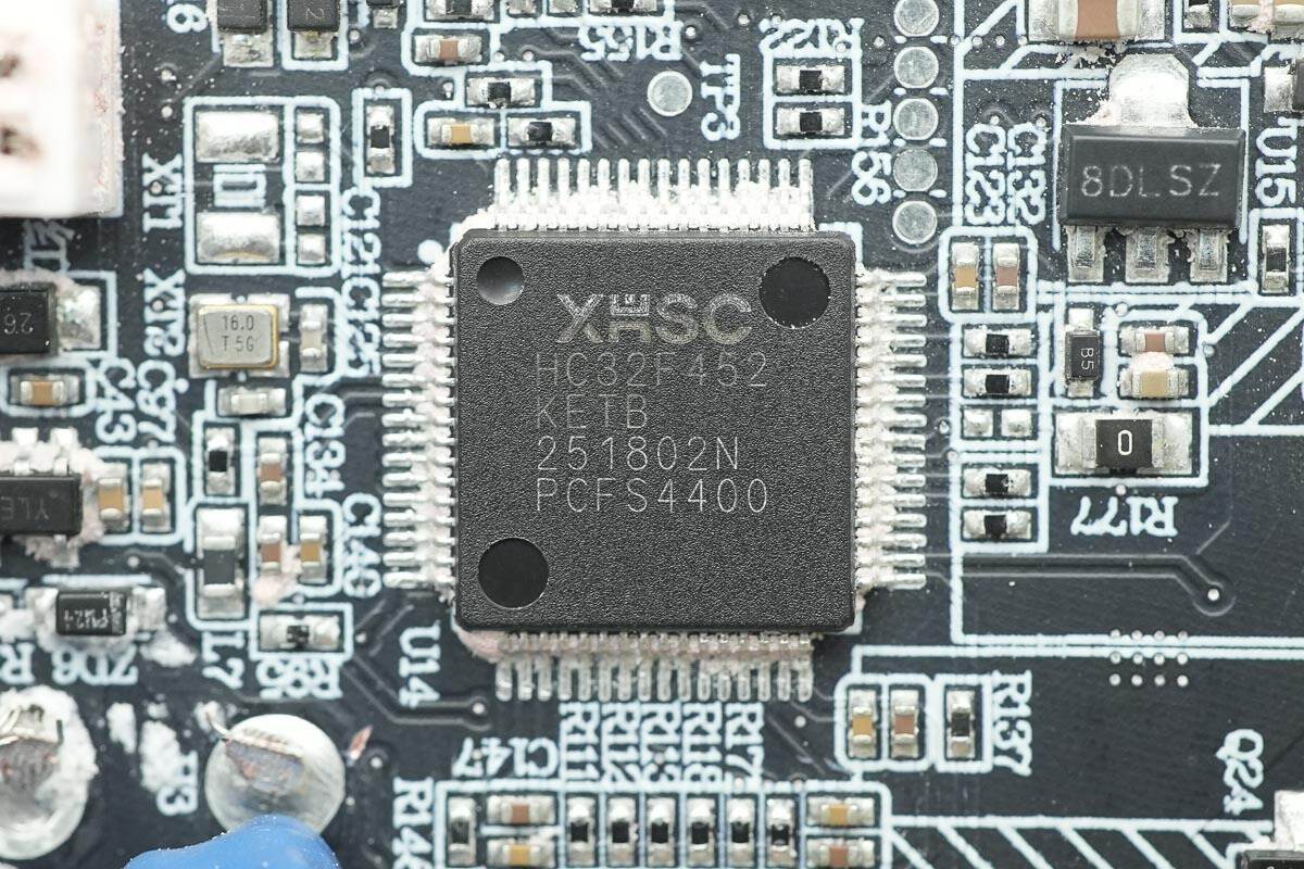
The MCU used for overall system control is from XHSC, model HC32F452KETB-LQFP64. The HC32F45x series features a high-performance 32-bit ARM Cortex-M4 core, with a maximum operating frequency of up to 200MHz. It integrates high-speed on-chip memory and a rich set of peripheral functions, supporting a wide voltage range (1.8-3.6V), a broad temperature range (-40°C to 105°C), and various low-power modes.
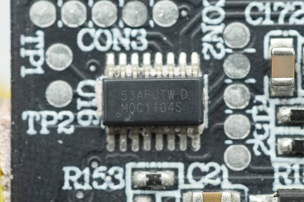
The MCU is from TI, model MSPM0C1104, part of the MSP ultra-low-power 32-bit MCU series. This series is based on the enhanced Arm Cortex-M0+ core platform, offering high-performance analog peripheral integration. The MCU operates at a maximum frequency of up to 24MHz, supports a temperature range of -40°C to 125°C, and runs on a power supply voltage range of 1.62V to 3.6V.
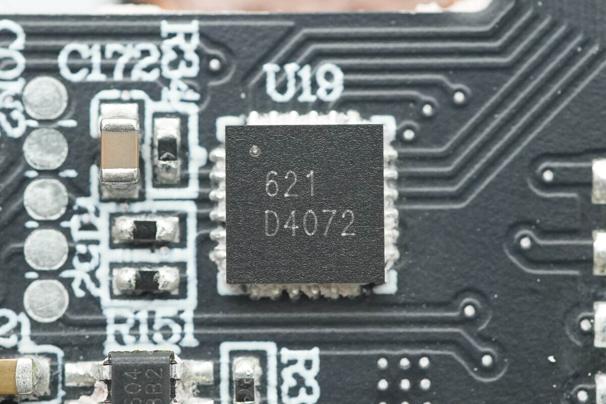
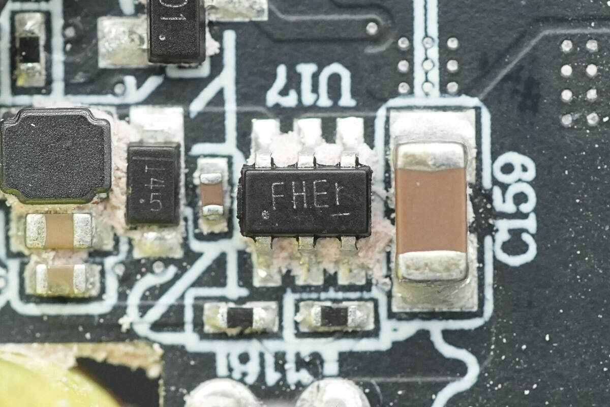
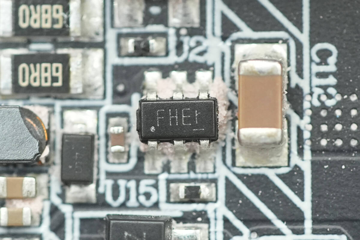
Close-up of the chip marked with 621.
The synchronous buck converter is from ETA, model ETA2850S2G, and it comes in a SOT23-6 package.
Close-up of the ETA ETA2850S2G synchronous buck converter.
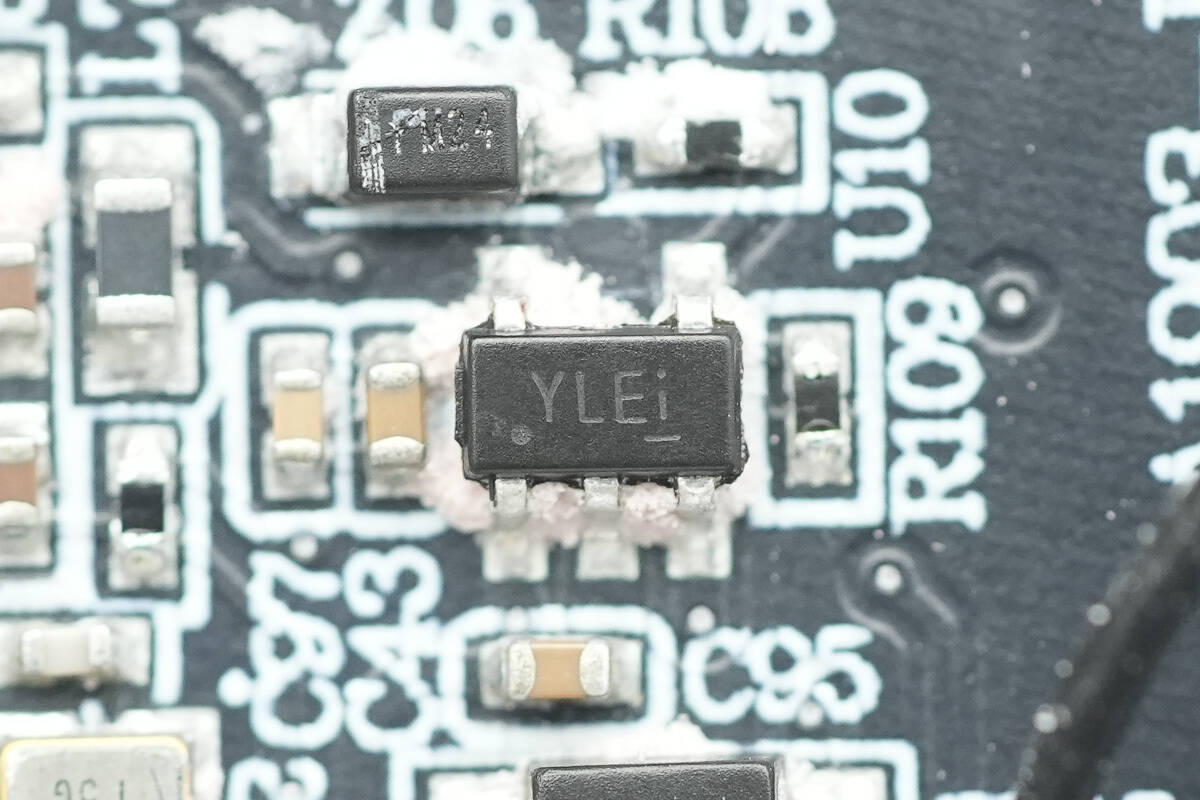
Close-up of the chip marked with YLEi.
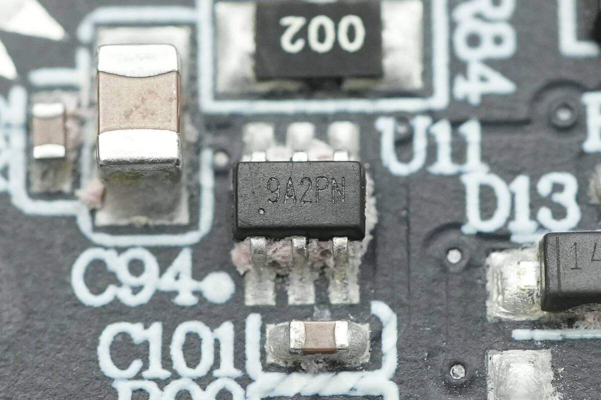
Close-up of the chip marked with 9A2PN.
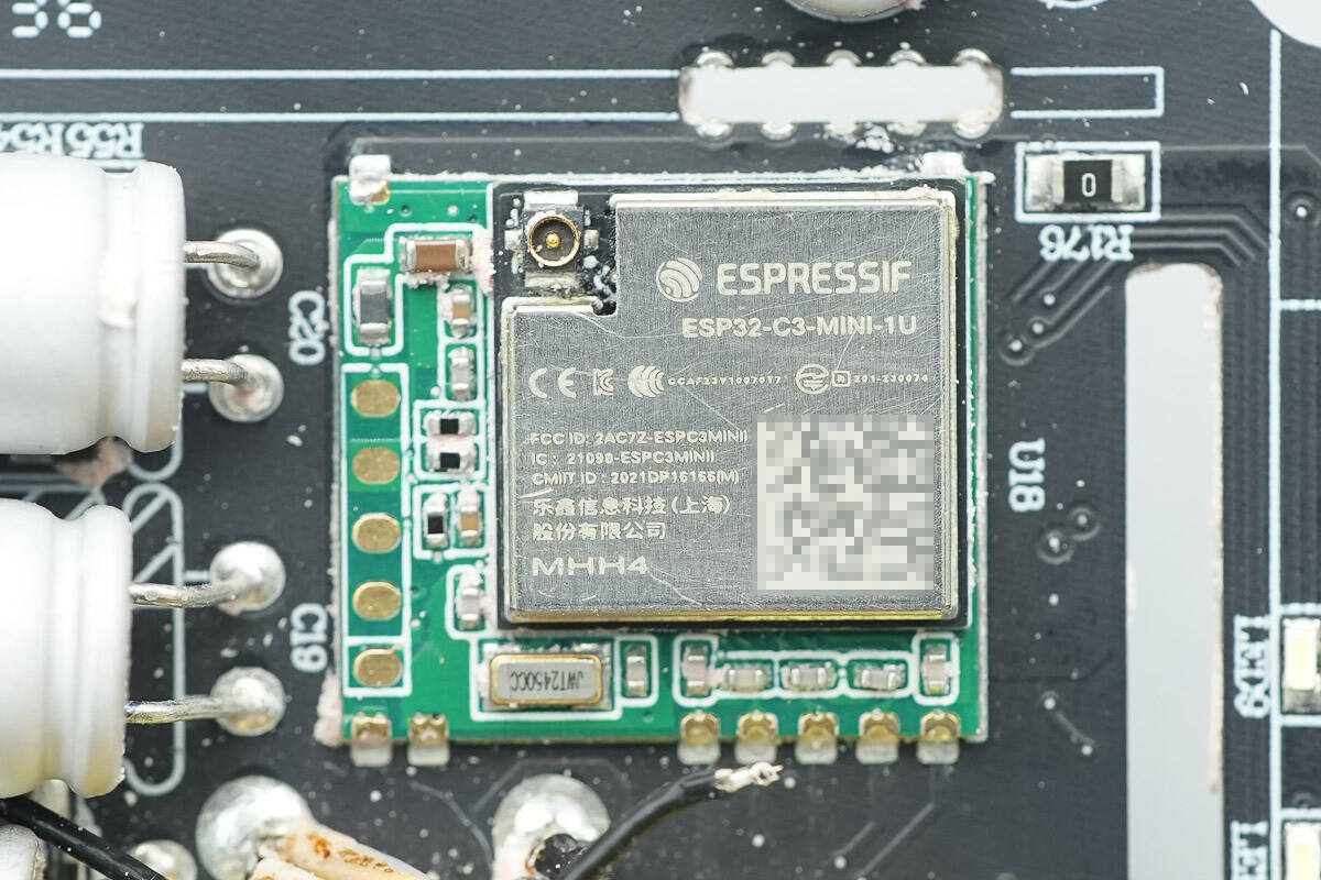
The wireless communication module is from ESPRESSIF, model ESP32-C3-MINI-1U, which supports both WiFi and low-power Bluetooth connectivity.
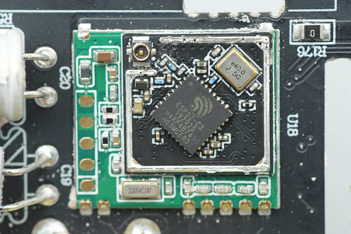
After removing the shielding cover, the interior contains the wireless communication chip and the crystal oscillator.
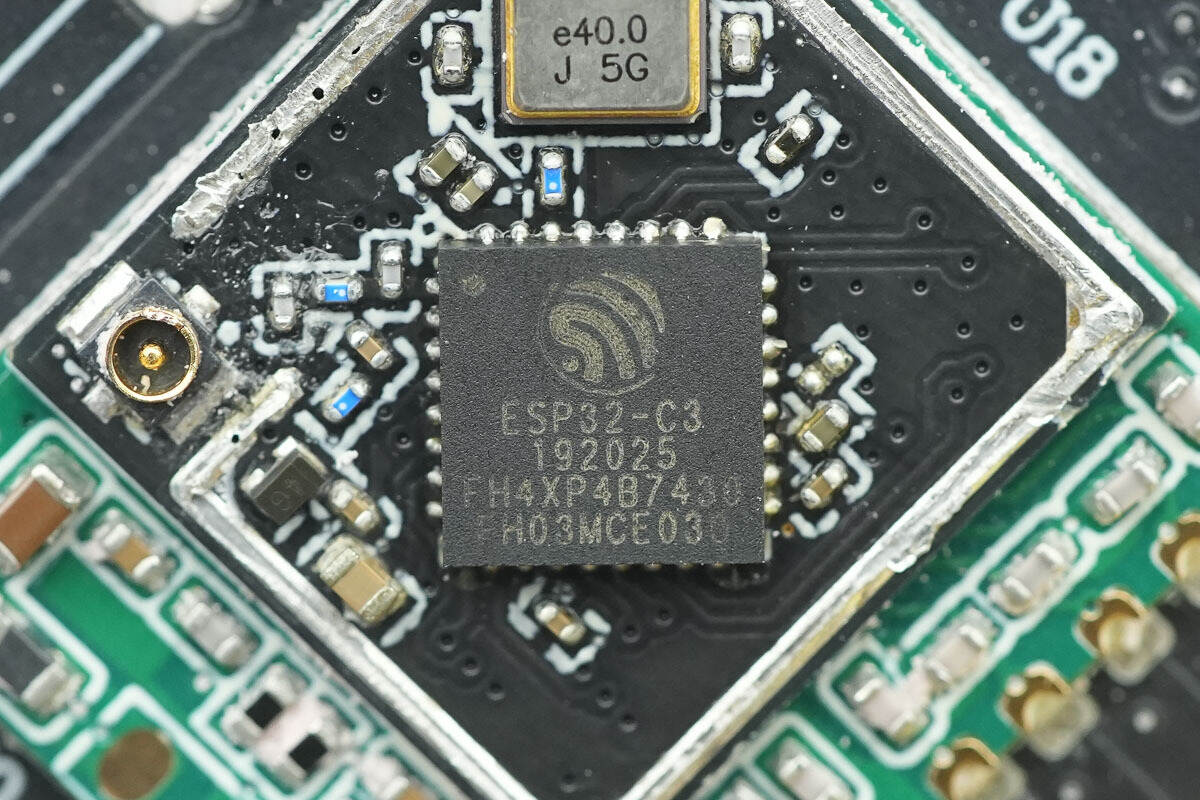
The wireless communication chip is from ESPRESSIF, model ESP32-C3. It is a low-power, highly integrated SoC that integrates 2.4GHz WiFi and low-power Bluetooth communication. The chip features a 32-bit RISC-V single-core processor running at a frequency of 160MHz, and it includes 384KB ROM, 400KB SRAM, 8KB SRAM, and 4KB eFuse. It comes in a QFN32 package.
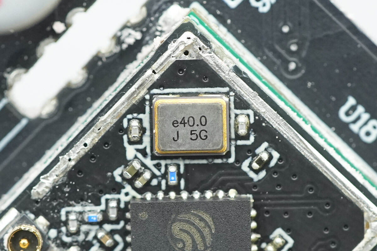
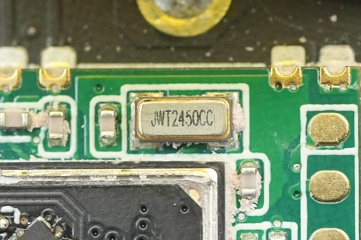
Close-up of the 40.0MHz SMD crystal oscillator.
Close-up of the 32.768kHz SMD crystal oscillator.
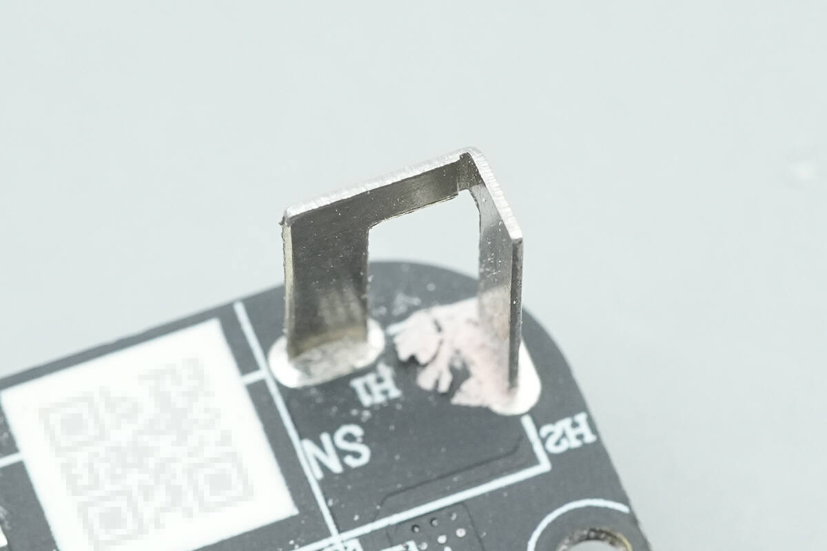
Close-up of the wireless antenna.
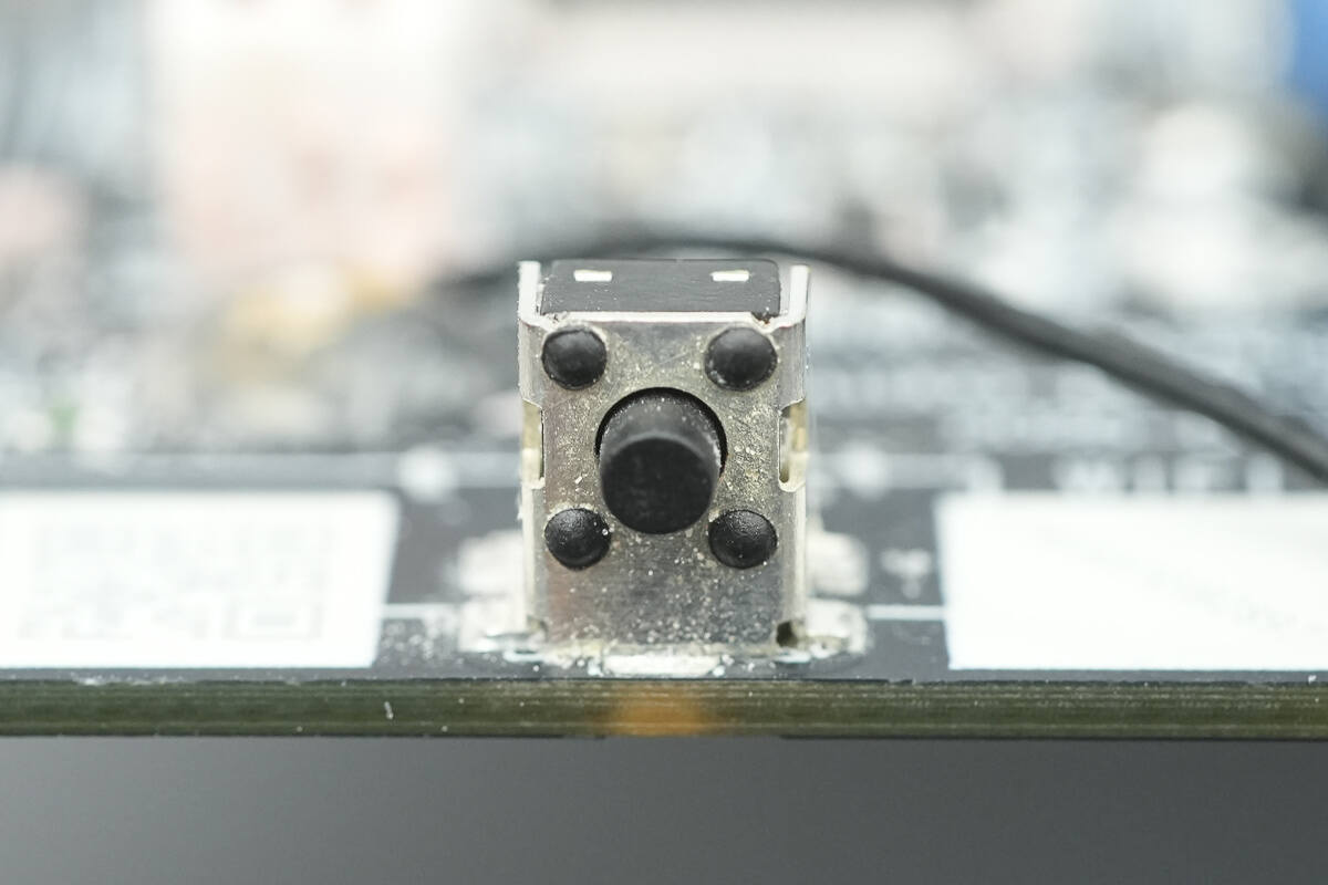
The reset button is surface-mount soldered.
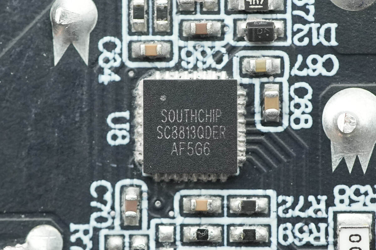
The synchronous buck controller adopts the SouthChip SC8813, which integrates an I2C interface for configuration of operating modes and runtime parameters. The SC8813 supports a very wide input and output voltage range, making it suitable for applications using 1–4 series lithium-ion batteries.
In charging mode, when the input voltage is higher than the battery voltage, the device steps down the input voltage to efficiently charge the battery. The SC8813 supports automatic trickle charging, constant-current charging, and constant-voltage charging management. In discharge mode (reverse boost mode), the SC8813 is capable of delivering a boosted output voltage of up to 36 V.
Here is the information about SouthChip SC8813.
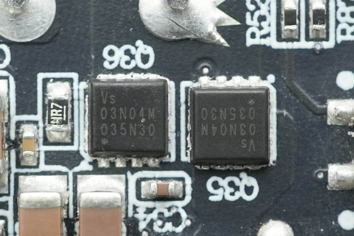
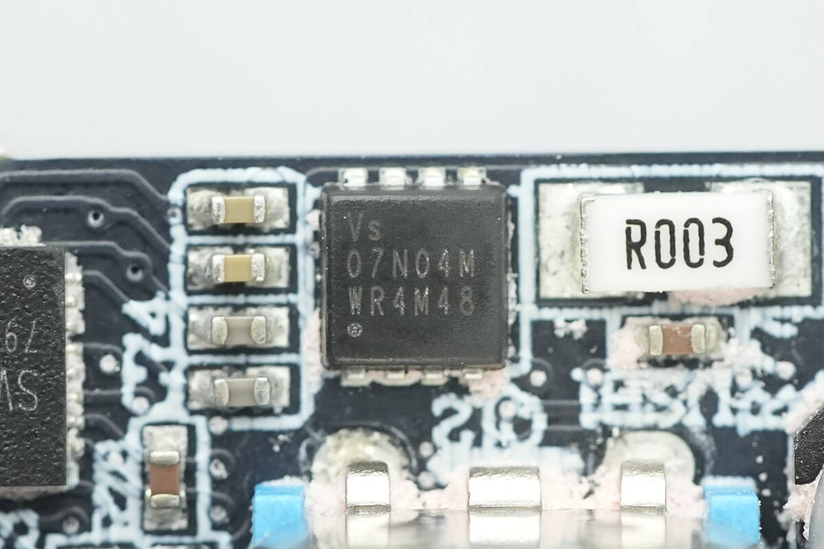
The two paired synchronous buck MOSFETs are from Vergiga, model VSE003N04MSC-G. They are N-channel MOSFETs rated at 40 V, with an on-resistance of 2.3 mΩ, and are housed in a PDFN3333 package.
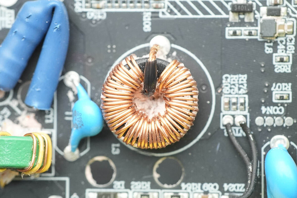
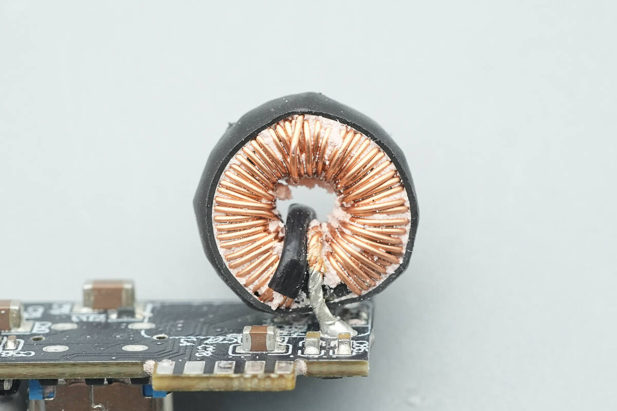
Close-up of the matched buck inductor.
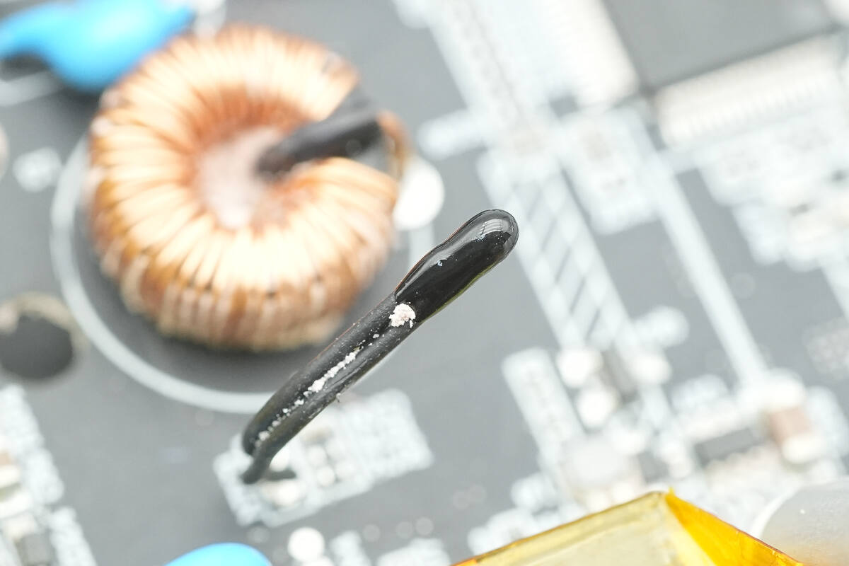
Close-up of the thermistor.
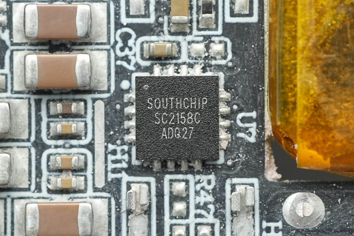
The PD controller used for Pogo Pin output control is from SouthChip, model SC2158C, and is packaged in a QFN16 form factor.
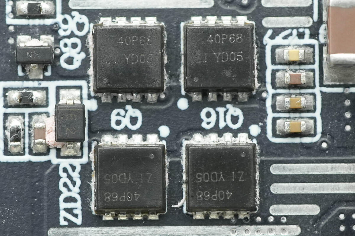
The four VBUS MOSFETs are from LEADTECK, model LT40P68FL. This is an enhancement-mode PMOS device rated at −40 V, with a continuous drain current of −48 A and an on-resistance of 10.5 mΩ. It is suitable for applications such as backlight driving, power management, and DC-DC buck-boost circuits.
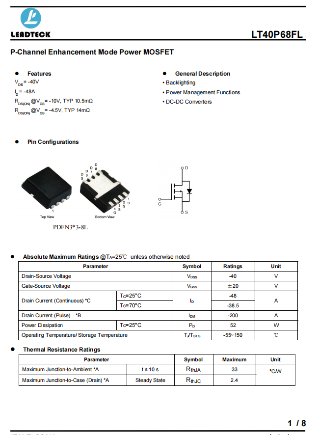
Here is the information about LEADTECK LT40P68FL.
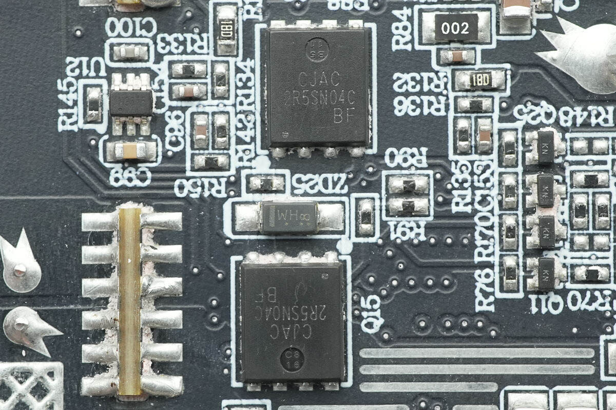
The other two VBUS MOSFETs are from JSCJ, model CJAC2R5SN04C. They are N-channel MOSFETs rated at 40 V, with an on-resistance of 2 mΩ, and are packaged in a PDFNWB 5 × 6 mm, 8-lead form factor.
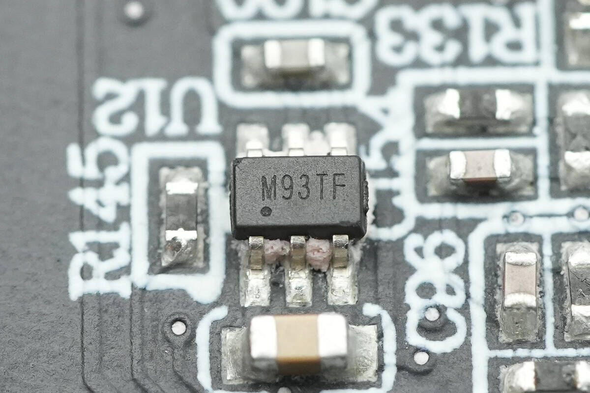
A current-sense amplifier from SGMICRO, marked with “M93,” model SGM8199A2, is used. It supports both high-side and low-side applications, provides bidirectional current sensing, operates with a supply voltage of up to 28 V, and is packaged in an SC70-6 form factor.
On the front side of the PCB where the USB sockets are located, components such as the buck protocol chip, synchronous buck MOSFETs, and solid capacitors are populated.
The rear side is populated with the buck protocol chip, synchronous buck MOSFETs, and buck inductors.
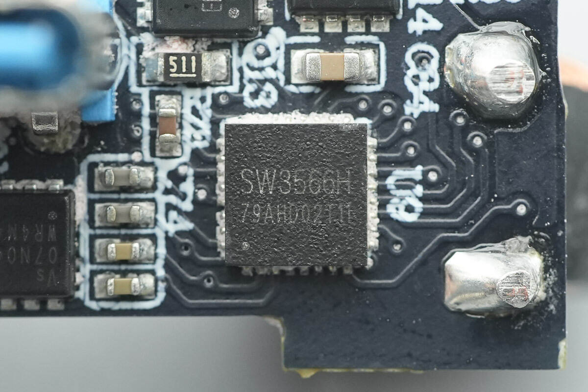
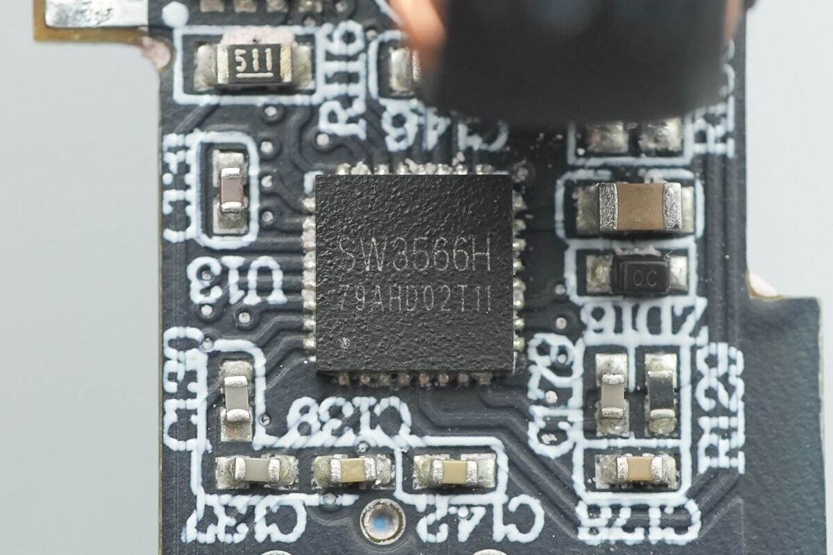
The buck protocol chip used for USB-C1 is from iSmartWare, model SW3566H. It is a highly integrated dual-port fast-charging SoC that supports both USB-C and USB-A charging, with independent current limiting for each port. The chip integrates a high-efficiency synchronous buck converter, supporting 20 V / 7 A and 28 V / 5 A outputs, and is compatible with fast-charging protocols including PD 3.1, QC, SCP, and UFCS. Custom fast-charging protocol configuration is supported, with a maximum output power of up to 140 W.
The SW3566H integrates CC/CV control, dual-port management logic, and bus voltage detection. When paired with external buck MOSFETs and VBUS MOSFETs, it enables dual-port buck output operation. The internal buck converter operates at a switching frequency of 180 kHz and supports both PWM and PFM modes. Protection thresholds such as output current and cable loss compensation can be configured via the I2C interface. An integrated ADC provides nine channels for sampling parameters, including input voltage, output voltage, output current, and chip temperature, and supports connection to an external MCU for parameter display.
The SW3566H supports an input voltage of up to 36 V and a maximum output current of 7 A. It integrates soft start, input overvoltage and undervoltage protection, output overvoltage and undervoltage protection, output overcurrent and short-circuit protection, DP/DM/CC overvoltage protection, overtemperature protection, external NTC thermistor protection, and power-limiting protection. The device is packaged in a QFN 4 × 4 mm, 32-pin package.
Here is the information about iSmartWare SW3566.
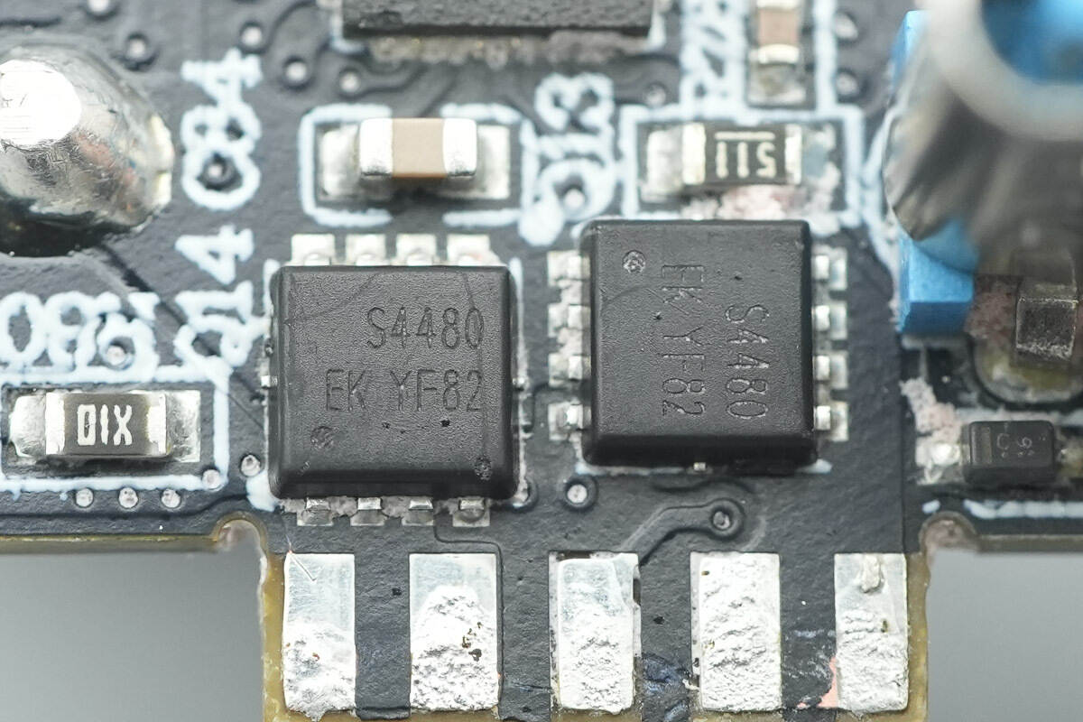
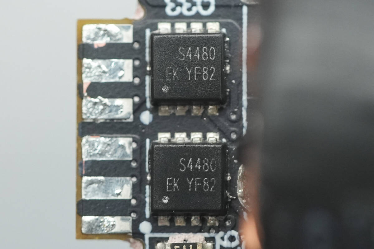
The two paired synchronous buck MOSFETs are from LEADTECK, marked with “S4480,” model LTS4480FLA. They are N-channel MOSFETs rated at 40 V, with an on-resistance of 5.6 mΩ, and are packaged in a PDFN 3 × 3 mm, 8-lead form factor.
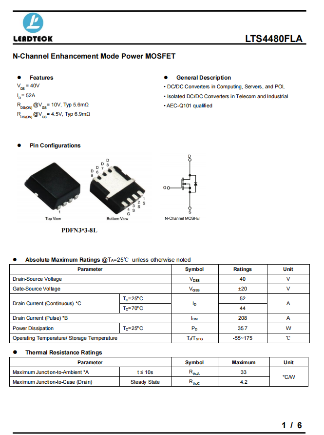
Here is the information about LEADTECK LTS4480FLA.
The buck inductor is insulated with a heat-shrink tube for protection.
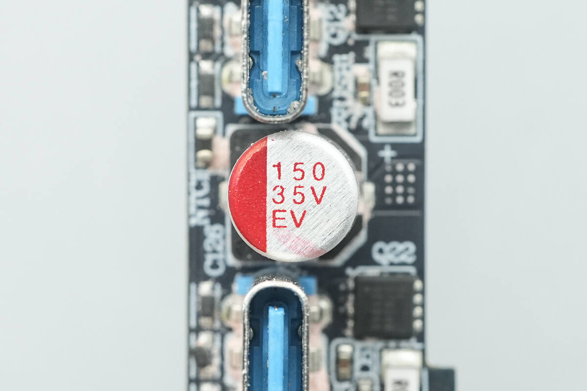
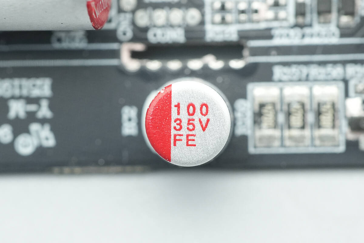
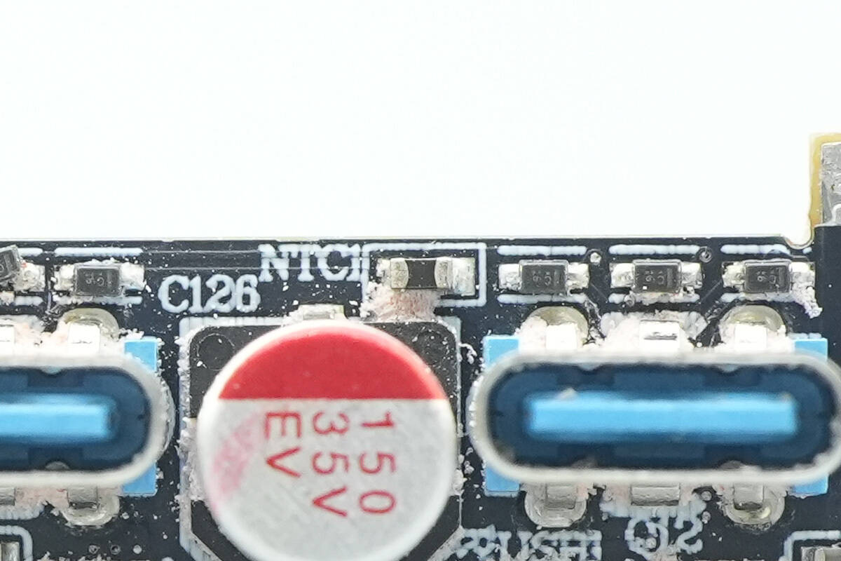
The solid capacitor used for output filtering has a specification of 35 V, 150 μF.
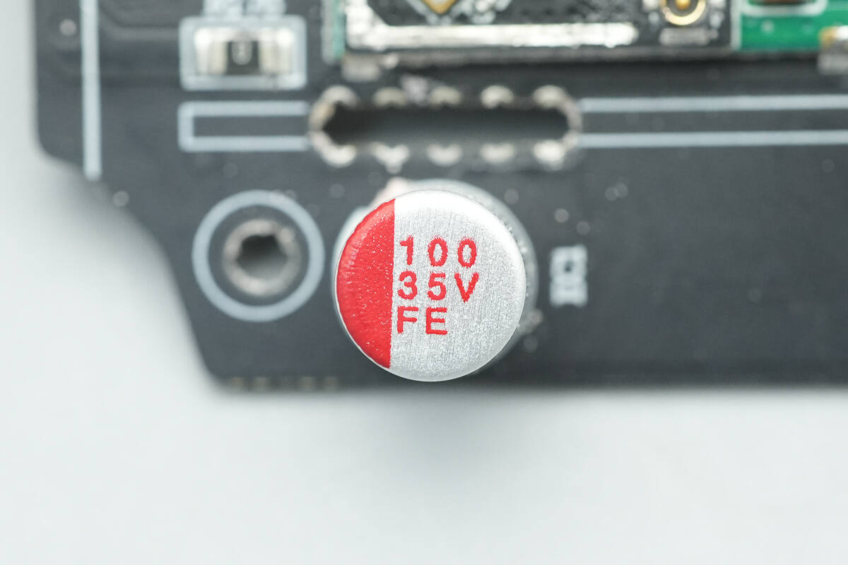
The other solid capacitor has a specification of 35 V, 100 μF.
The buck protocol chip for both USB-C2 and USB-A ports is also the iSmartWare SW3566H.
The synchronous buck MOSFETs for both USB-C2 and USB-A ports are also LEADTECK LTS4480FLA.
Close-up of the matched buck inductor.
The solid capacitor used for output filtering has a specification of 35 V, 150 μF.
The other solid capacitor has a specification of 35 V, 100 μF.
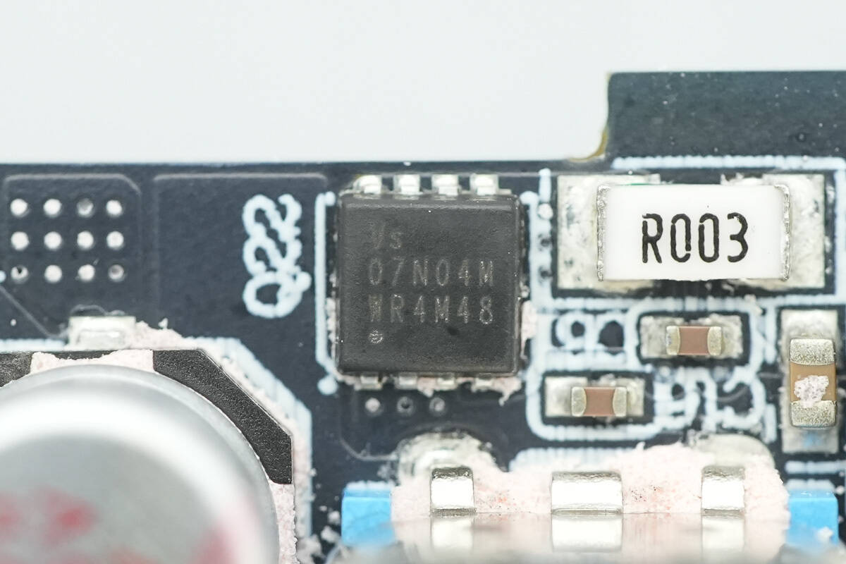
The USB-C1 output VBUS MOSFET is from Vergiga, model VSE007N04MS-G. It is an N-channel MOSFET rated at 40 V, with an on-resistance of 3.2 mΩ, and is packaged in a PDFN3333 form factor.
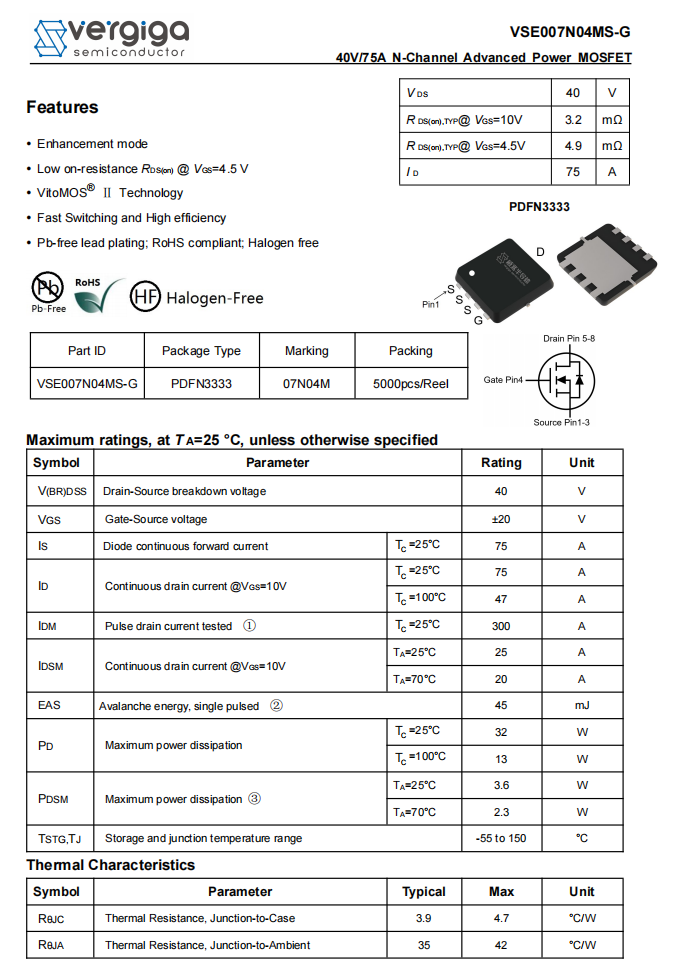
Here is the information about Vergiga VSE007N04MS-G.
The output VBUS MOSFET for USB-C2 also uses the Vergiga VSE007N04MS-G.
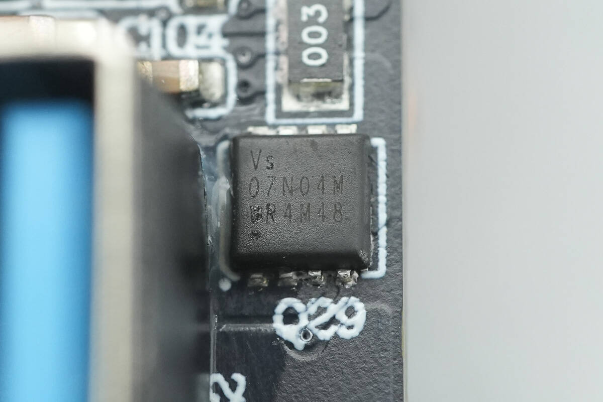
The output VBUS MOSFET for USB-A also uses the Vergiga VSE007N04MS-G.
A thermistor is placed near the USB-C sockets for temperature monitoring.
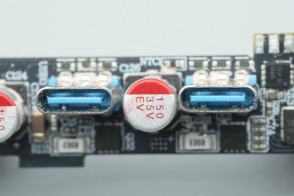
Close-up of the two USB-C sockets.
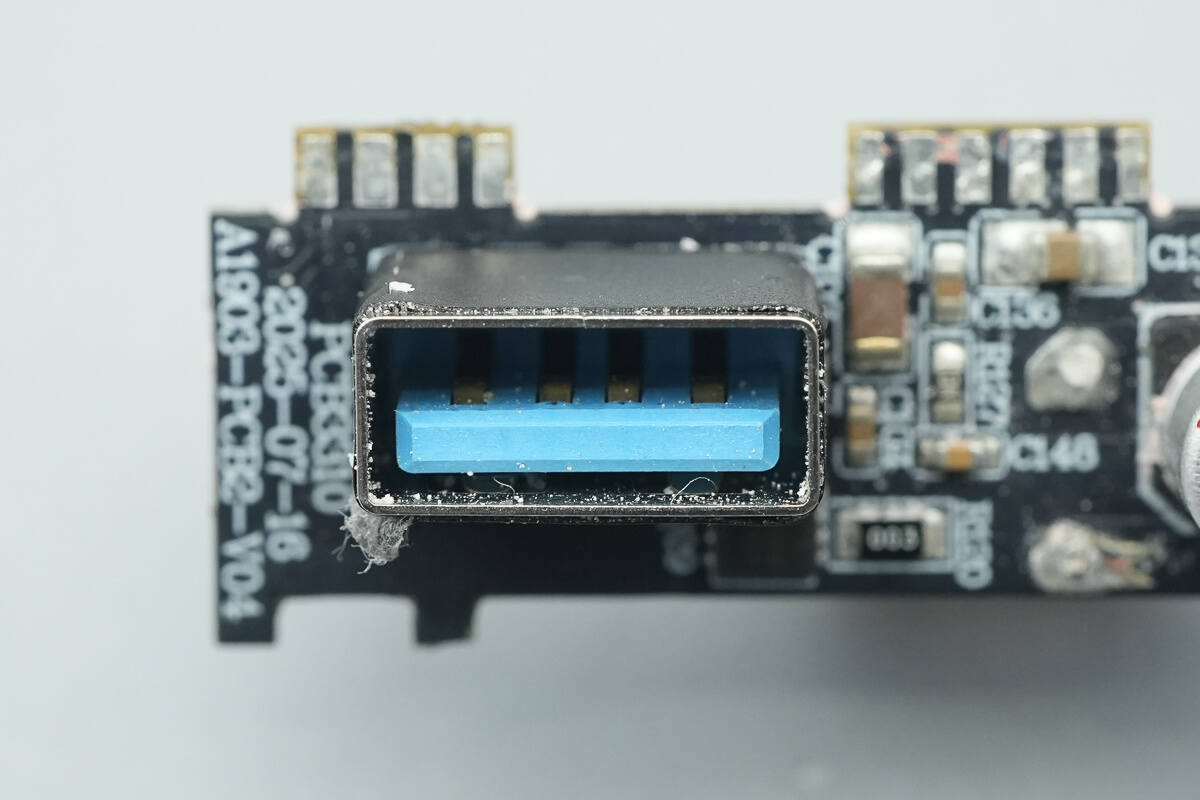
The USB-A socket housing is treated with insulation.
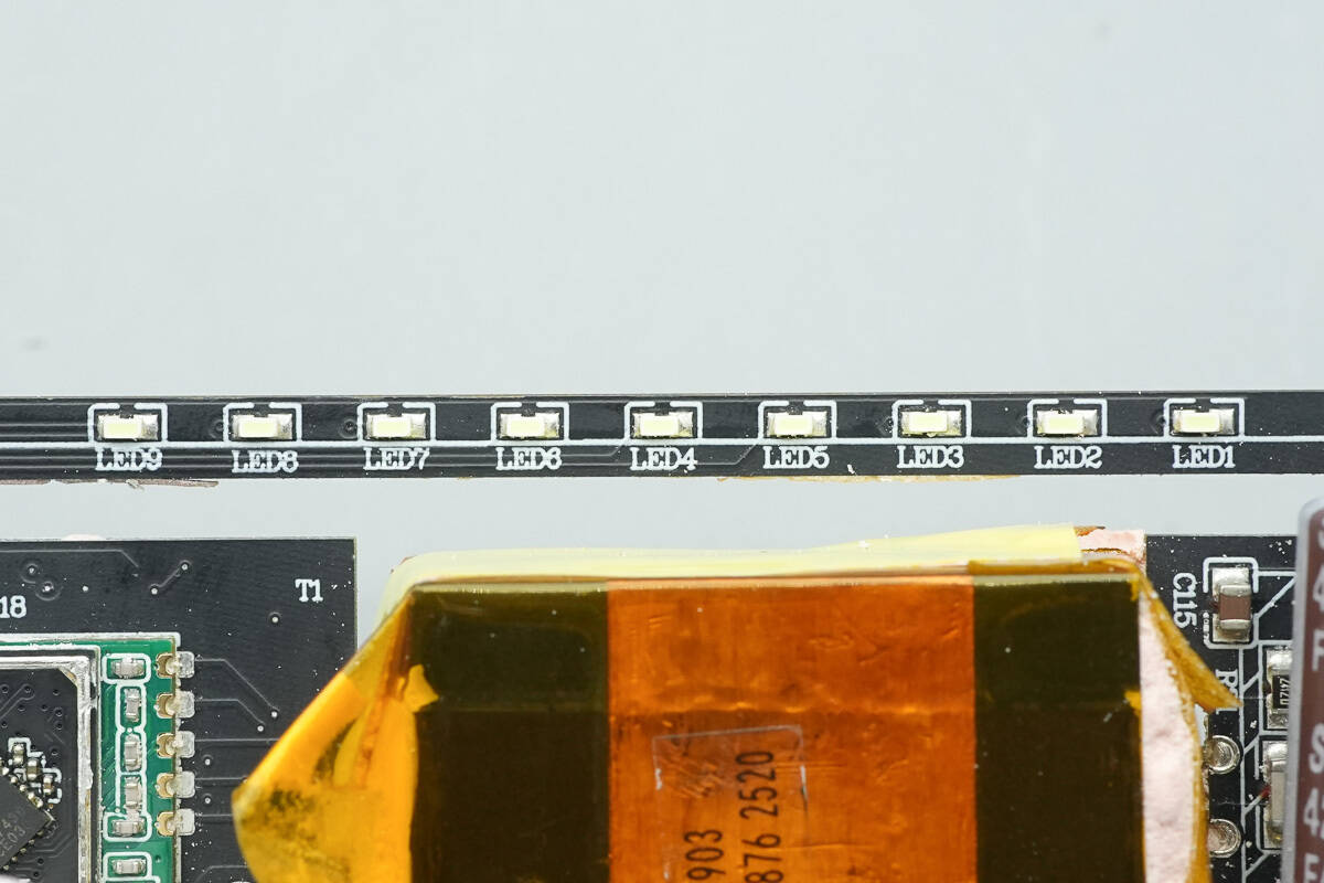
Close-up of the LED indicators.
Well, those are all components of the Anker Prime 150W Charging Station.
Summary of ChargerLAB
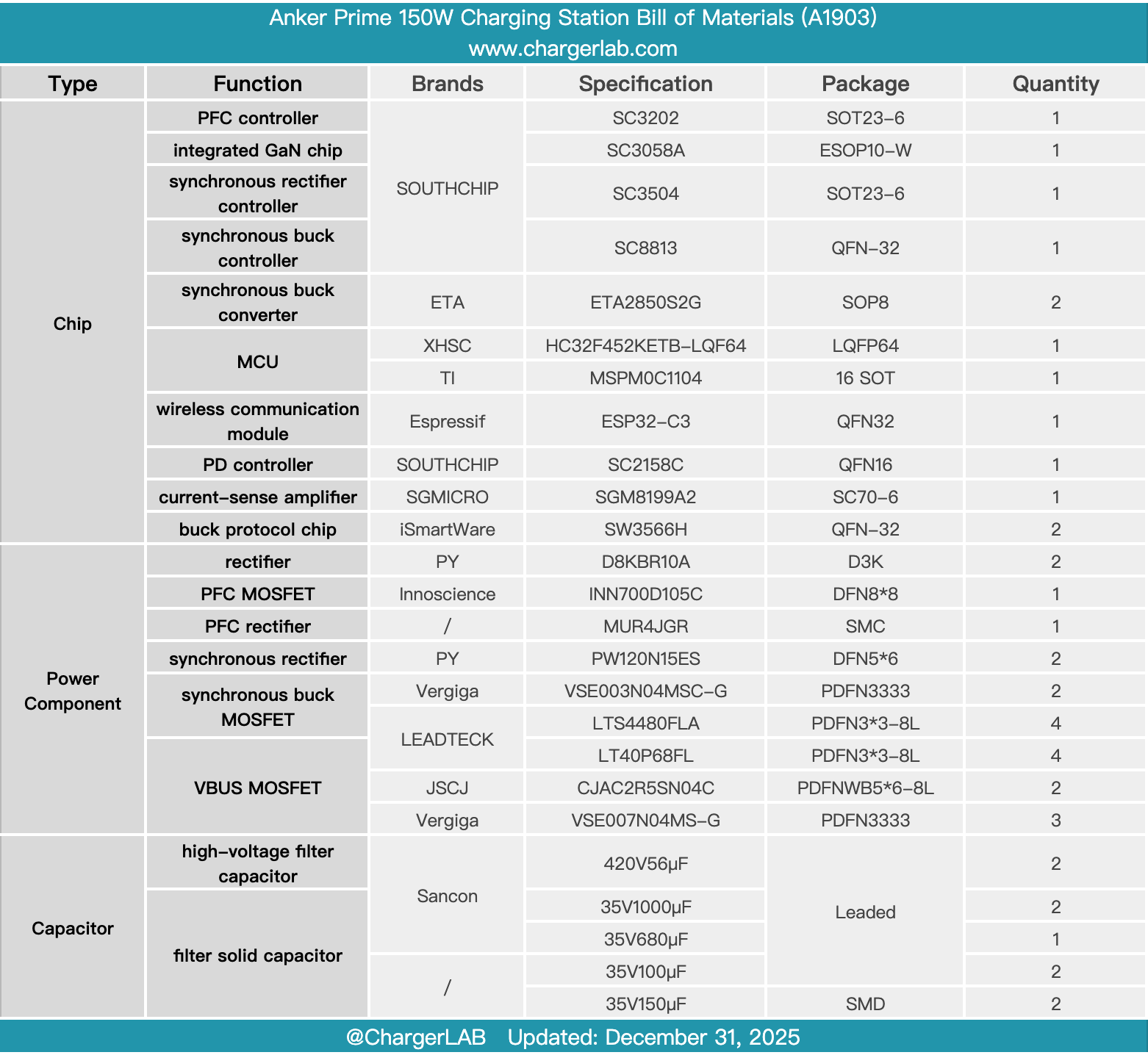
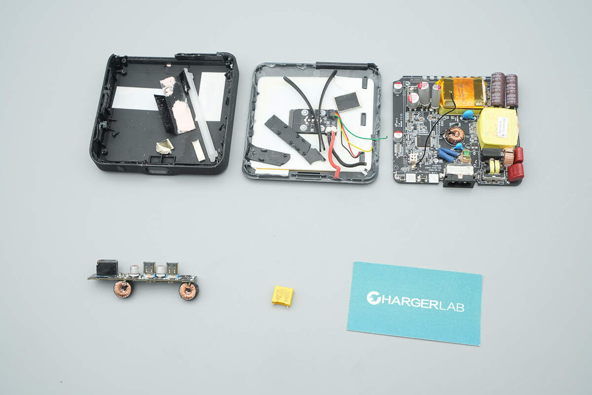
Here is the component list of the Anker Prime 150W Charging Station for your convenience.
It features a slim, flat form factor with a minimalist design. It is equipped with two USB-C ports and one USB-A port, supporting output powers of 140W, 100W, and 22.5W, respectively, and is compatible with fast-charging protocols including QC 3.0, FCP, SCP, AFC, PD 3.1, and PPS.
Its core strengths lie in strong expandability and one-touch management via the app. The Pogo Pin array on the top supports magnetic attachment, allowing supported devices to be easily aligned and placed. It also supports simultaneous charging and discharging, effectively adding an output interface. Through the mobile app, users can flexibly customize device settings and view charging data, performance curves, and temperature rise information, delivering a highly convenient and refined user experience.
After taking it apart, we found that it is designed based on a SouthChip SC3202 + SC3058A + SC3504 power solution. The Pogo Pin output adopts a SouthChip SC8813 buck topology, controlled by the SC2158C PD controller. The three USB ports use two iSmartWare SW3566H devices for secondary buck conversion and fast-charging protocol identification, and output control. An XHSC main control MCU and an ESPRESSIF wireless communication module are also employed.
The modules are potted with thermally conductive adhesive, and graphite thermal pads are applied to assist heat dissipation. Overall, the build quality and component selection are solid and reliable.
Related Articles:
1. Teardown of Anker Prime 160W Charger with Smart Display (A2687)
2. Teardown of Anker Nano 75W Car Charger (A2738)
3. Teardown of DJI Power 1000 Mini Power Station (DYM1000M)