As the go-to media authority in consumer power technology, ChargerLAB delivers rigorous, exhaustive teardowns that pull back the curtain on the internal chipsets and PCBA engineering of today's most popular hardware. To showcase the technical precision behind these teardowns, this article takes you step-by-step through a standard Lenovo power bank analysis inside our testing lab.
From non-destructive unboxing and precision physical measurements to capturing core mixed-signal SoCs and inductor arrays via macro photography, our workflow strips away the casing to expose the true circuit architecture and safety components. The goal is to provide engineers and tech enthusiasts worldwide with invaluable, first-hand technical intelligence, while firmly reminding the public: lithium-ion battery teardowns are dangerous and strictly "do not try this at home."
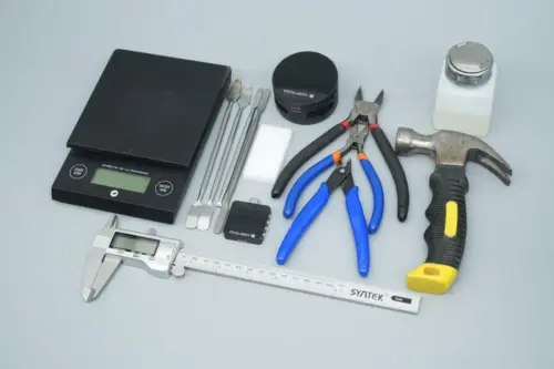
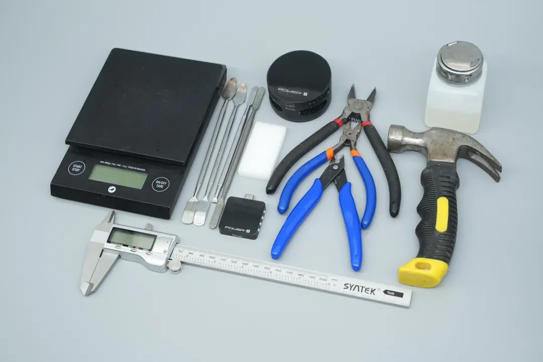
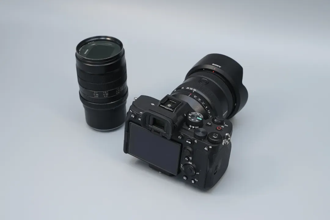
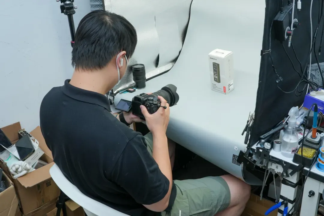
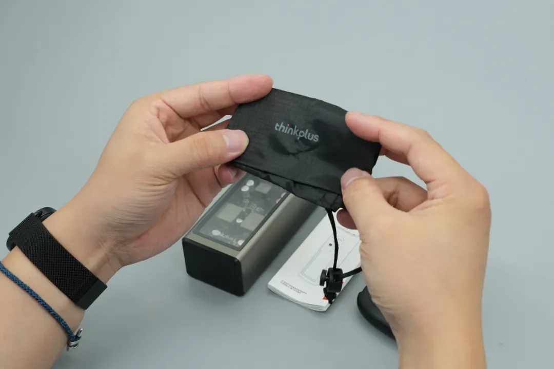
A world-class teardown demands high-end testing equipment alongside strict anti-static and non-destructive protocols. Our preparation begins with calibrating a Sony A7M4 full-frame camera and studio lighting, while precisely logging multi-port fast-charging protocols, dimensions, and weights using digital scales, calipers, and POWER-Z testers.
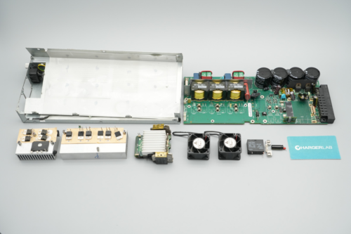
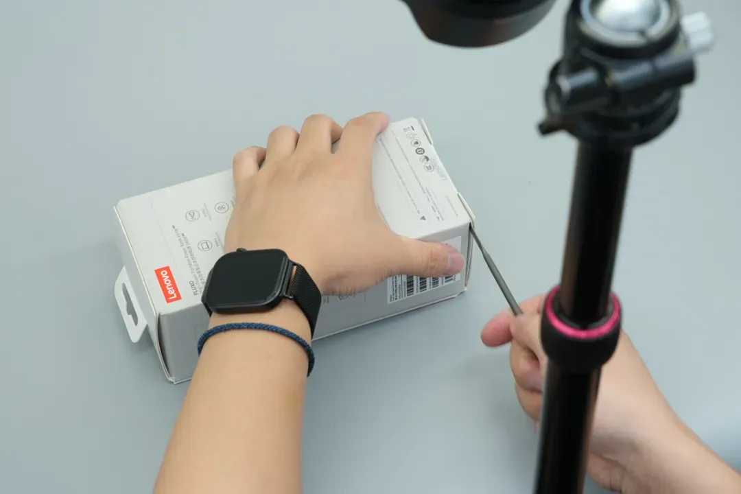
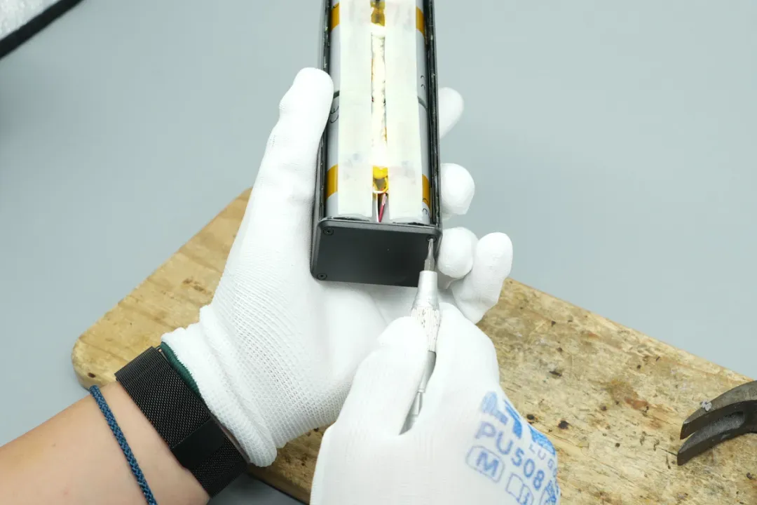
When cracking open ultra-sonically welded or reinforced enclosures, technicians wear anti-static gloves, utilizing anhydrous alcohol to soften adhesives and insulated tools to gently release ribbons. This guarantees that the high-density polymer cells and fragile surface-mount components remain entirely pristine as the PCBA is extracted.
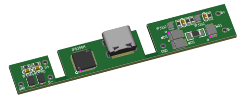
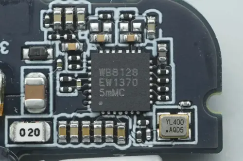
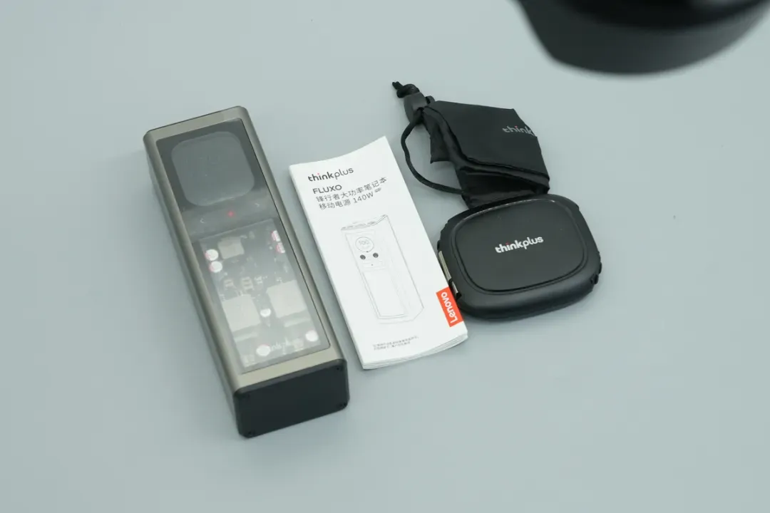
Next, combining portable LED fill lights with macro lenses, we carefully clean away residual chip encapsulate to reveal the authentic laser markings on vital power components. The process wraps up with a complete "family portrait" layout documenting everything from the outer packaging to the motherboard, battery cells, and housing.
More than just a hardware showcase, ChargerLAB’s standardized teardown process marries industrial engineering with environmental sustainability. Once photography and technical analysis conclude, our engineers arrange the disassembled components into custom shadow boxes mapped to the original circuit topology.
Paired with detailed annotations, these components are transformed into educational "electronic art," ensuring that harvested hardware avoids the landfill and serves a higher purpose.
As the new national standard for power banks rolls out alongside advanced bi-directional fast-charging topologies, our deep-dive teardowns and supply chain analysis will continue to tackle industry challenges head-on—fueling the next generation of safe, high-quality innovation in portable power and mobile computing.
Related Articles:
1. ChargerLAB POWER-Z KM003C E-Marker Function Now Supports CH253
2. ChargerLAB POWER-Z Reveals the Fast Charging Protocols of the AMC Technology PD3.2 240W GaN Charger
3. ChargerLAB POWER-Z Reveals the Fast-Charging Protocols of the Xiaomi UltraThin 10000mAh Power Bank