Introduction
ChargerLAB is diving into Belkin’s latest 3-in-1 wireless charger—a device that brings Qi2.2 technology and unparalleled ecosystem flexibility to your desktop.
Belkin is a veteran in the multi-device charging space, known for its diverse range of stand, flat, and tree-style charging stations. This latest model stands out as a true innovator, pairing Qi2.2 wireless charging with a highly adaptable watch charging experience.
The headline feature is its customizable retractable watch module. It ships with a set of adapters designed to hold original charging pucks from Apple, Google, and Samsung. By housing the original watch charger inside the retractable unit and powering it via an internal USB-C port, Belkin solves the fragmentation issue for users juggling different smartwatch ecosystems.
Having previously dismantled a 20W Qi2 2-in-1 magnetic charger, we are excited to peel back the layers of this new 3-in-1 station to see how Belkin has engineered this level of integration and quality.
Product Appearance
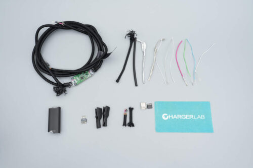
The package includes the Belkin 3-in-1 wireless charger unit, a single-port USB-C power adapter with a maximum output of 45W, an original USB-C to USB-C power cable, four sets of silicone adapter gaskets for various smartwatches, and the user manual and warranty card.
Designed in a clean, pure white, the unit sports a sleek tapered-base silhouette. Its premium skin-friendly finish provides a luxurious touch and keeps the device fingerprint-free.
The charger’s flat circular top is home to the Qi2.2 wireless charging module, featuring the Belkin logo front and center.
The top wireless charging module is fully adjustable, tilting to your preferred angle. Flip it up to uncover the hidden charging spot designed specifically for TWS earbuds.
The side of the chassis features a retractable locking mechanism designed to secure the mobile wireless charging module.
The four provided smartwatch charging adapter gaskets.
The included original USB-C to USB-C power cable is equipped with a cable tie for convenient storage.
Two hidden USB-C ports are located within the recessed area at the base of it, alongside detailed technical spes:
Product Name: UltraCharge Modular Charging Dock
Model: WIZ052
Input: 15V⎓3A (Max)
USB-C Output: 5V⎓2A
Country of Origin: Vietnam
Various certification markings are printed on the other side of the base, including Qi2, CE, NOM, and FCC—indicating compliance with safety standards across multiple regions.
Product Spotlight
The standout feature here is the customizable, retractable watch charging module on the side. Simply pull it out to access a circular mounting port, custom-fit for your original watch charger regardless of the brand.
Simply thread your original watch charger through the side module, plug the USB-C end into the hidden port inside the base, and tuck any excess cable neatly into the integrated management channel.
The setup with the matching gaskets and watch charger is illustrated here—a truly ingenious design.
The top provides magnetic wireless charging for smartphones, the lower panel is designated for AirPods, and the side retractable module powers the smartwatch.
Snap the iPhone 17 Pro onto the top Qi2.2 module, and the signature wireless charging animation appears instantly.
ChargerLAB POWER-Z KM003C shows that the iPhone 17 Pro pulling 14V 2.09A at 31.13W, successfully triggering full-speed Qi2.2 fast charging.
When testing multi-device charging, the unit hits 14.88V at 2.09A for a total of 31.19W, easily handling the demands of charging multiple devices at once.
Physical Specifications
The maximum diameter of the charger base is about 80.68mm (3.176 inches).
The height of the charger is about 67.01mm (2.638 inches).
The diameter of the top-cover Qi2.2 module is about 58.93 mm (2.320 inches).
The weight is about 214.1g (7.55 oz).
With the design overview and performance testing complete, it's time to go under the hood—join ChargerLAB as we dive into the teardown of this unit.
Internal Construction
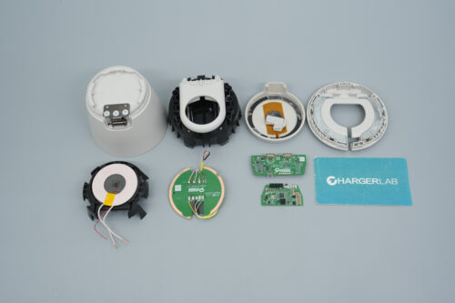
Removing the base cover reveals the internal assembly. The interior is secured by multiple screws around the perimeter, with the PCBA vertically mounted onto the internal bracket.
The interior of the removed base cover features two semi-circular, heavy metal counterweights. These are integrated to increase the overall weight and lower the center of gravity, preventing the charger from lifting when a mobile device is detached.
Two USB-C female connectors are soldered onto the PCBA. One serves as the external power input interface, while the other provides a 5V power output to the smartwatch charging module.
The connection between the mainboard and the upper charging module is established via multiple wires, with all solder joints reinforced by potting compound.
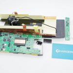
Separate the various parts of the unit one by one.
With the central watch charging support frame removed, the guide rails for the side retractable watch charging module are fully exposed and clearly visible.
Push the watch charging module to reveal the internal mechanism, which employs two long springs that serve as both the retraction damping and recoil mechanism; the mechanical design is exceptionally robust.
Disassembling the upper section reveals multiple cables are routed through the hinge mounting point to connect to the top Qi2.2 magnetic wireless charging module. Located beneath are the Litz wire and NTC thermistor associated with the earphone wireless charging assembly.
The top TWS wireless charging module contains a tightly wound wireless charging coil, featuring a centrally mounted NTC thermistor to monitor the temperature in real time during charging.
The Qi 2.2 wireless charging module is disassembled into the outer cover, the wireless charging coil (featuring a green PCB and magnetic shielding plate), and the underlying base chassis.
The back of the Qi2.2 wireless charging coil features a magnetic shielding plate and an NTC thermistor. The interior of the housing features a layer of yellow FPC (Flexible Printed Circuit) for charging status detection, complemented by a peripheral circular magnet array designed for precision magnetic alignment.
The Qi2.2 wireless charging module is from CPS. In the rear folding hinge area, all solder joints are reinforced with potting compound to ensure structural integrity.
Extracting the PCBA reveals a dual-layer stacked PCB architecture.
Separating the two PCBs reveals a connection established via pin headers.
The lower PCB is primarily responsible for TWS wireless charging watch power output, with two USB-C female ports, VBUS MOSFETs, and other components on the top.
The back is populated with wireless charging transmitter ICs, protocol chips, and other associated components.
The upper PCB is populated with wireless charging ICs, authentication chips, wireless charging power MOSFETs, and other components.
There are no components on the back.
PCBA Analysis
The Qi 2.2 wireless charging SoC, model CPS8610, is from CPS. It is a highly integrated transmitter controller/SoC designed for Qi 2.2 MPP 25 W applications, supporting power levels up to 30 W. This single-chip solution handles protocol processing, power stage driving, measurement links, and multi-channel demodulation.
The CPS8610 supports Qi 2.0/2.2 standards and is compatible with major proprietary ecosystems. On the wired side, it integrates support for PD 3.1 PPS, QC, AFC, and UFCS protocols. It performs voltage stepping and power mapping based on input capabilities to balance efficiency, thermal performance, and compatibility across the entire power range, facilitating platform-level reuse.
It is housed in a QFN31 package and is suitable for applications such as automotive magnetic charging mounts and multi-in-one wireless charging devices.
The authentication chip is from CPS, model CPS1010, which is a wireless charging protocol encryption chip specifically designed for Qi-certified applications.
It integrates a SHA256 cryptographic engine, ECC signature capability, and a TRNG for key generation. It provides robust identity and security authentication for wireless charging devices and is housed in a DFN8 package.
Two NMOSs are from GigasTech, models GTMW8030A-NQ and GTMW8030D-NQ, respectively. The wireless charging resonant cap is positioned adjacent to them.
The GTMW8030A-NQ is a single N-channel MOSFET designed for resonant cap switching. It features an 80V breakdown voltage and a 30A rated current. Manufactured using SGT tech, it achieves a low on-resistance of just 13mΩ and is housed in a PDFN3.3*3.3-8L SMD package.
Here is the info about the GigasTech GTMW8030A-NQ.
The GigasTech GTMW8030D-NQ, a dual N-channel enhancement-mode power MOSFET that integrates two MOSFETs into a single package. It features an 80V breakdown voltage, a 30A rated current, and is manufactured using SGT tech. It offers an on-resistance of 13mΩ and is housed in a PDFN3.3*3.3-8L (Dual) SMD package.
Here is the info about the GigasTech GTMW8030D-NQ.
The protocol chip is from CPS, model CPS8849A, housed in a QFN24 package. This highly integrated fast-charging protocol chip supports PD 3.1, PPS, and Vconn power delivery. It is also compatible with the UFCS integrated fast-charging standard and various other protocols, including QC.
It features field-upgradability via CC or DPDM pins, supports master/slave I2C communication, and includes an FB pin for DC-DC converter control, enabling an output voltage range of 3-22V.
The CPS8849A integrates temperature monitoring and a low-side current sense amplifier. It supports Vconn power delivery and utilizes NMOS as a VBUS MOSFET.
It features multifunctional GPIO pins, programmable discharge current, primary-side AC voltage detection, and power limiting detection. It also provides programmable cable loss compensation, output OCP, and other protection features, making it suitable for charger and automotive charger applications.
The wireless charging IC is from CPS, model CPS8601, a high-efficiency wireless charging transmitter IC supporting an input voltage range of 3.3V to 14V. It is compliant with WPC 1.3 EPP 15W standards and supports fast wireless charging for Samsung and Apple devices. It integrates an 8051-based microcontroller core, 256B of RAM, 3KB of external RAM, 16KB of MTP, and 40KB of ROM.
The CPS8601 features an integrated 17mΩ low-resistance power MOSFET and supports adjustable dead-time control. It is equipped with dual I2C interfaces and dual UART interfaces, and supports both sleep and standby modes. The device includes comprehensive thermal and overvoltage protection, and is housed in a QFN3*4-24 package.
There are four wireless charging resonant caps.
A chip, marked KAWHDA.
The synchronous step-up chip is from SCT, model SCT12A2DHKR, housed in a DFN20 package. It is a highly efficient, fully integrated synchronous boost converter that supports an input voltage range of 2.7V to 20V and features a peak switch current capacity of up to 15A.
A power-switching control MOSFET, marked BR 120P03.
The VBUS MOSFET is from GigasTech, model GTM8205S, NMOS, 20V/6A and 18mΩ, and housed in a SOT23-6L package, it is highly optimized for battery protection and load switching applications.
Here is the info about the GigasTech GTM8205S.
Well, those are all components of the Belkin Qi2.2 3-in-1 Wireless Charger.
Summary of ChargerLAB
Belkin’s 3-in-1 wireless charger is a masterclass in design, blending vertical folding and telescopic versatility.
The standout feature is the side-loading watch charging module. With the included set of adapters, it seamlessly integrates the original chargers from Apple, Google, and Samsung. By routing power through an internal, hidden USB-C port, it eliminates cable clutter, making it the perfect solution for power users.
The build quality is equally impressive. A heavy metal base provides a rock-solid foundation, while the telescopic mechanism features smooth dual-spring rails. Under the hood, it leverages a comprehensive CPS wireless charging ecosystem, featuring the CPS8610 controller, CPS1010 authentication chip, and the CPS8601/CPS8849A protocol chips.
Efficiency is further bolstered by premium power components from GigasTech, including the GTMW8030A-NQ/D-NQ MOSFETs for cap switching and the GTM8205S for VBUS control.
In summary, this charger is as practical as it is stylish—a premium, highly compatible 3-in-1 solution that pairs sophisticated aesthetics with robust engineering.
Related Articles:
1. Teardown of the Anker737 MagGo 3-in-1 Wireless Charger
2. The Cable That Surfs the Web, GlocalMe Debuts the Unicord 3-in-1 Charging & Wi-Fi Solution
3. Stuffcool Launches Nexi – India’s most compact 3-in-1 Foldable Qi2.2 Magnetic Wireless Charger with 25W Fast Charging for iPhone, AirPods & Apple Watch