Introduction
DJI has launched a brand-new portable power station, the DJI Power 1000 Mini. It features a built-in 1 kWh lithium iron phosphate battery. The inverter delivers a rated output power of 1000 W, with a boosted output of up to 1200 W, enabling it to support high-power appliances. The inverter is also optimized for higher conversion efficiency at low loads, extending the operating time of low-power devices.
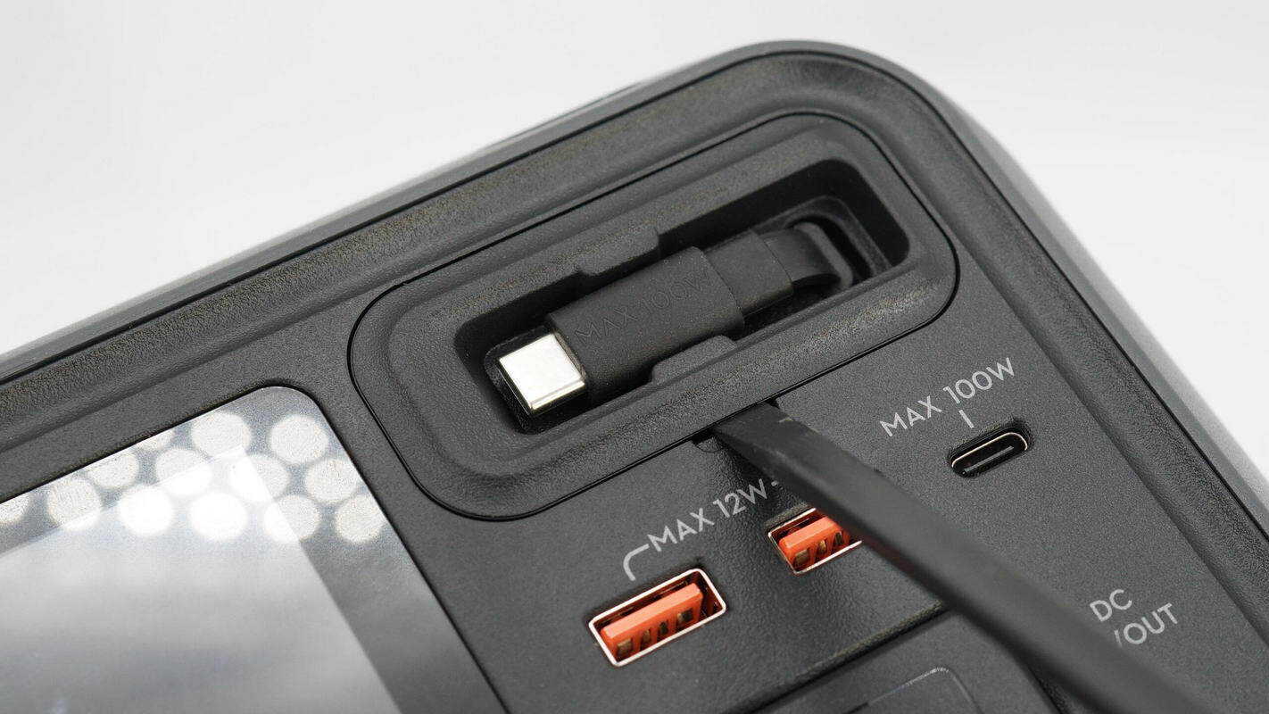
The power station supports AC charging, reaching 80% capacity from zero in just 58 minutes. It also supports 400 W fast charging via a vehicle, as well as charging through solar panels and USB-C. The unit is equipped with two universal AC output sockets and an integrated retractable USB-C cable, approximately 80 cm in length, enhancing convenience for everyday use. The retractable cable module is also detachable and replaceable.
The front panel includes additional USB-C and USB-A ports. The USB-C port supports 100 W bidirectional fast charging, while the USB-A port provides up to 12 W output. The SDC port supports a charging input of up to 400 W and a discharging output of up to 300 W. The inverter uses a fully potted protection design, ensuring reliable operation in environments such as seaside camping or high-altitude road trips. Next, we will present a teardown to take a closer look at its internal design and components.
Product Appearance
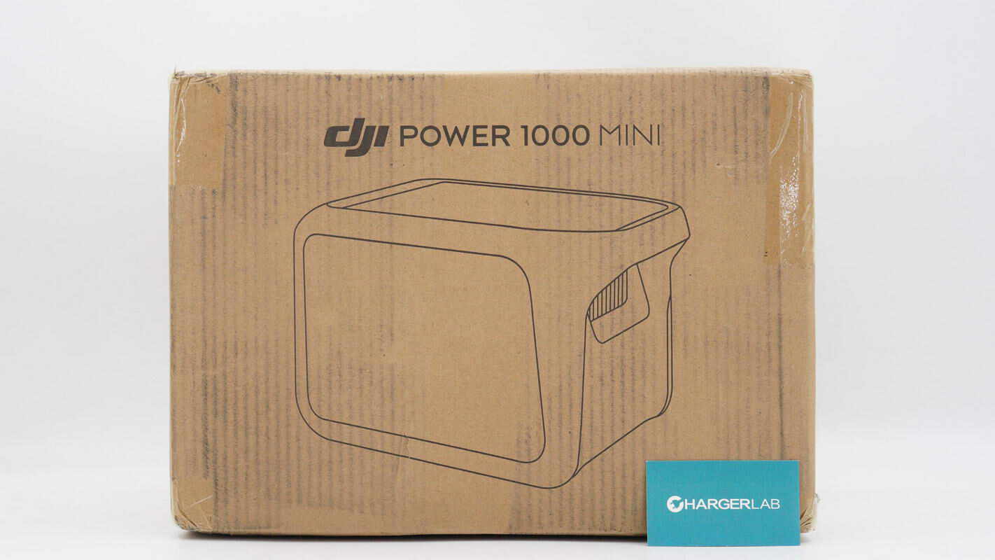
It is packaged in a corrugated cardboard box.
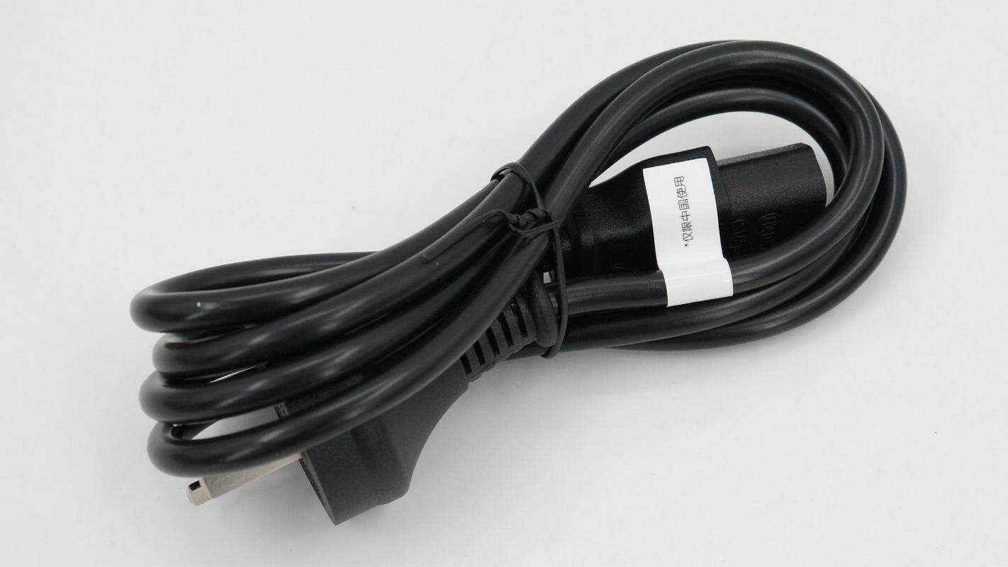
The included power cable is a three-prong type with a length of 1.5 meters, rated at 10A 250V~.
The design is minimalist, with a comprehensive set of functional interfaces. Combined with a 1 kWh battery capacity and 1000 W output power, it is well-suited to meet power needs in outdoor scenarios.
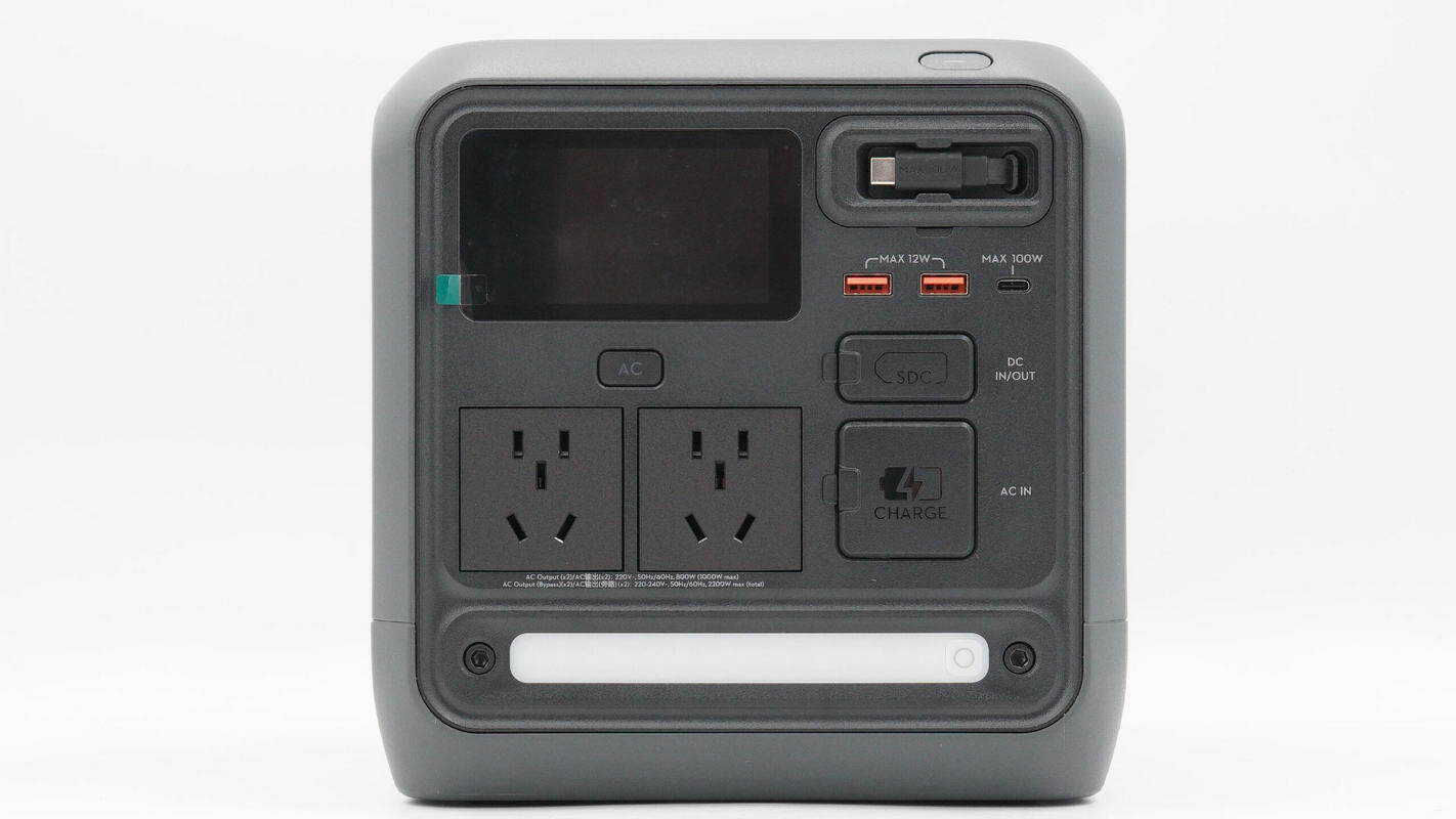
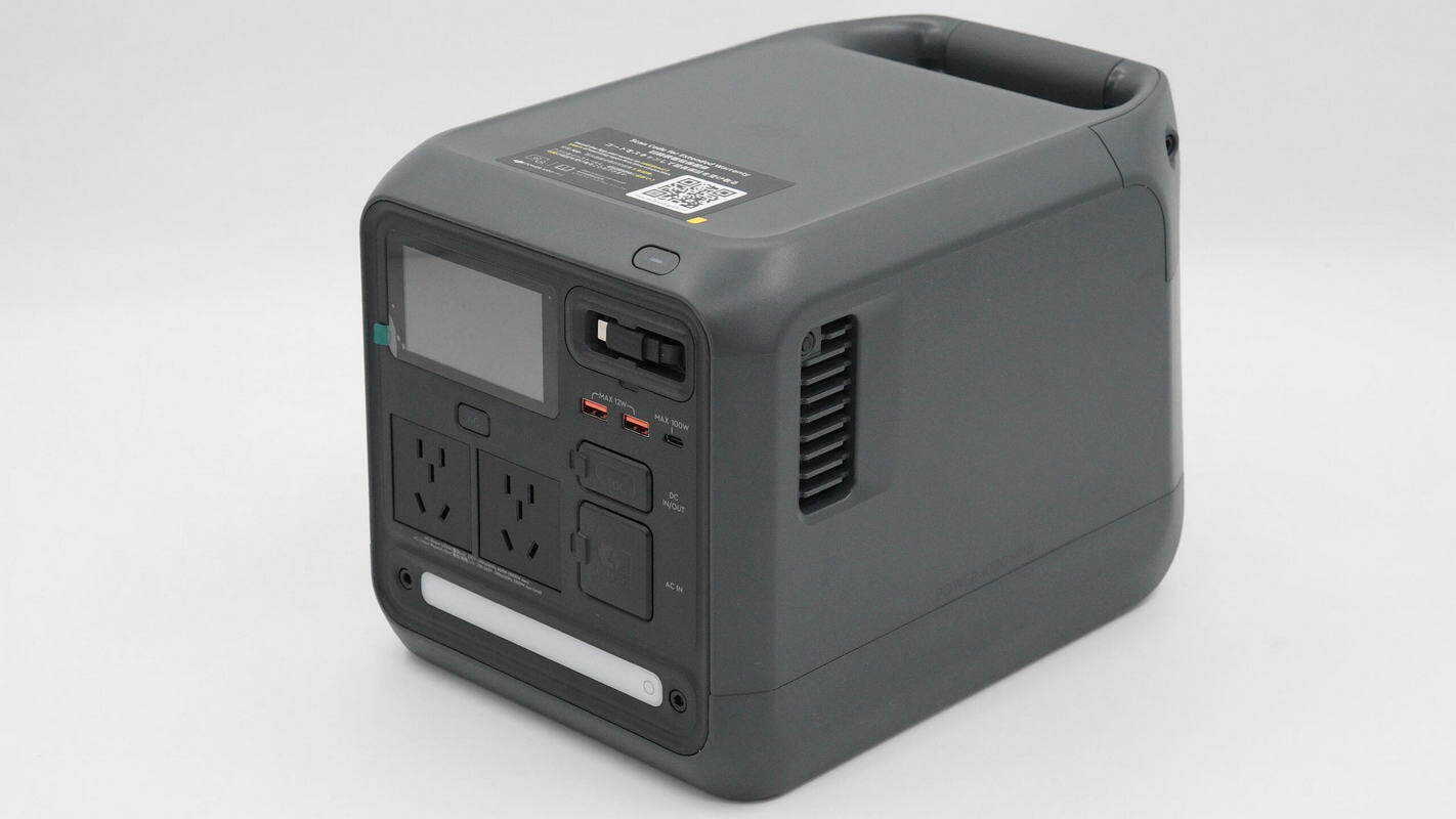
The front panel features an LCD in the upper left corner, with AC output sockets located below it. On the upper right is a retractable USB-C cable, while USB-A and USB-C ports are positioned beneath it. The SDC port and the AC input port are protected by sealing covers. At the bottom is an integrated LED light.
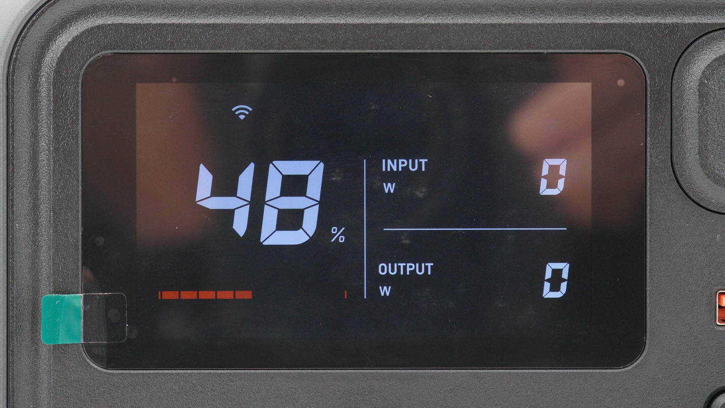
The display shows the remaining battery level, input and output power, and Wi-Fi connection status.

Above the two universal AC output sockets is a power control button, and below them, the rated output power is labeled as 1000 W, with a bypass output rating of 2200 W.

The retractable USB-C cable is magnetically secured and adopts a modular design, allowing it to be detached and replaced.

The two USB-A ports support up to 12 W output, while the USB-C port supports up to 100 W output.
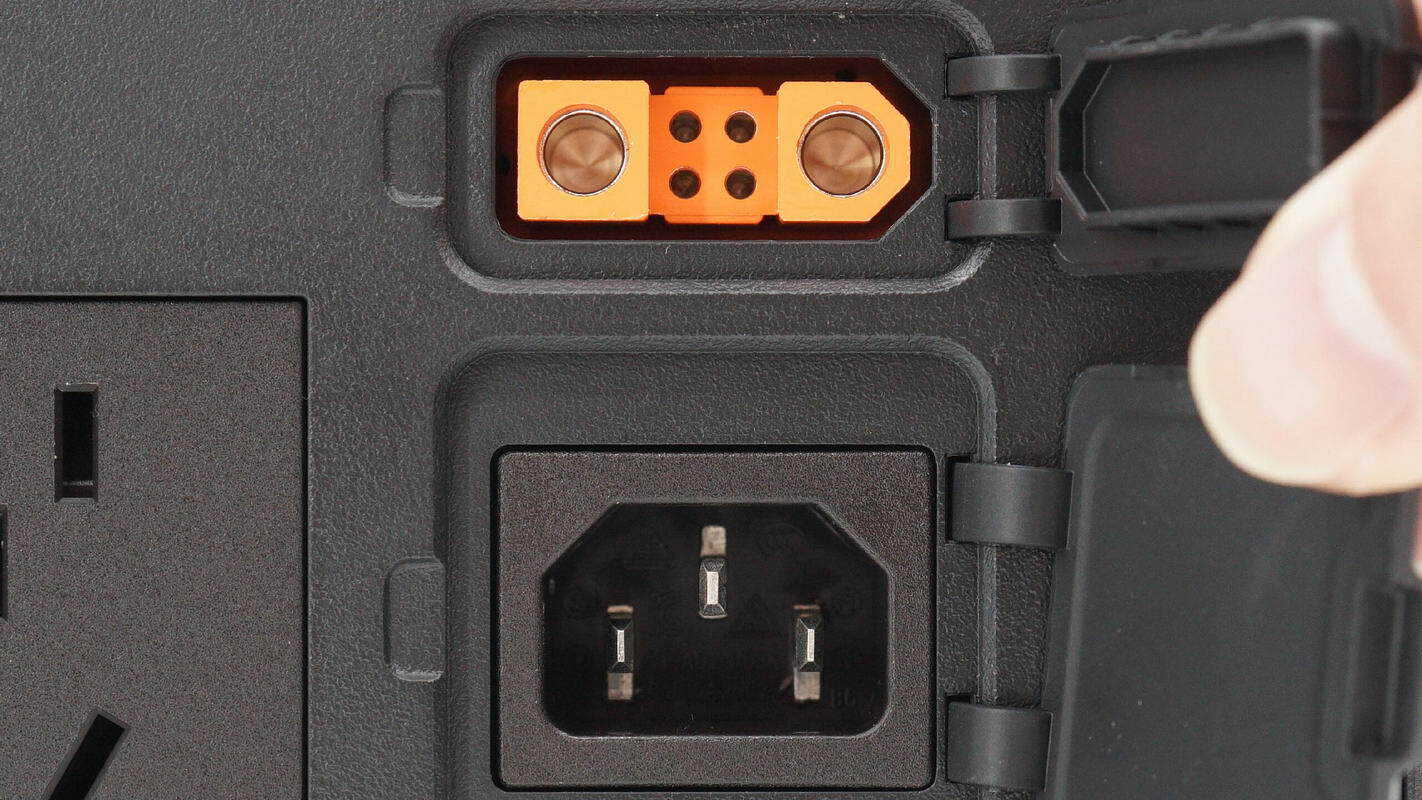
The SDC port and AC input socket are equipped with protective covers to prevent dust and moisture.
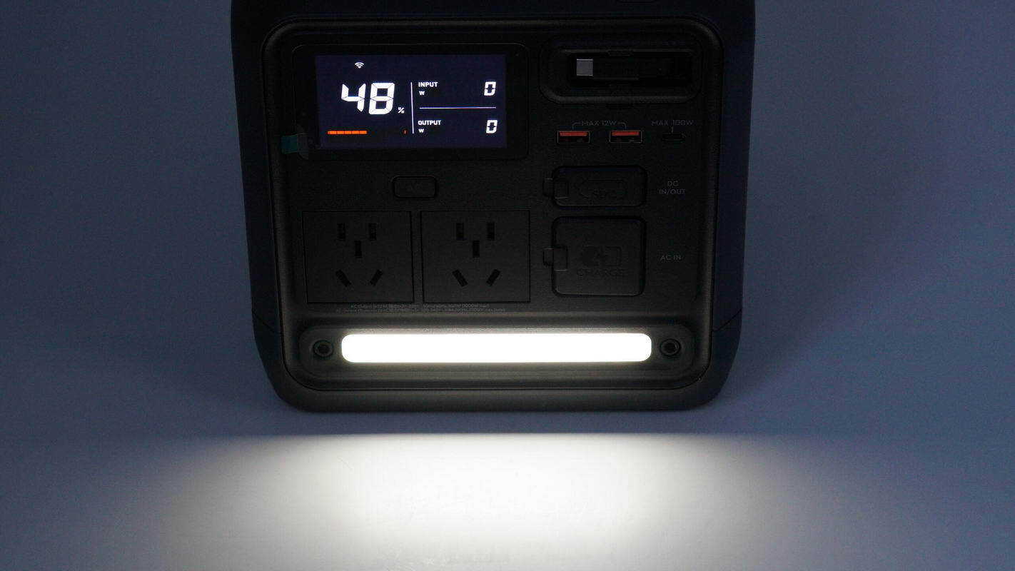
The LED light provides sufficient illumination for nighttime activities and emergency lighting.
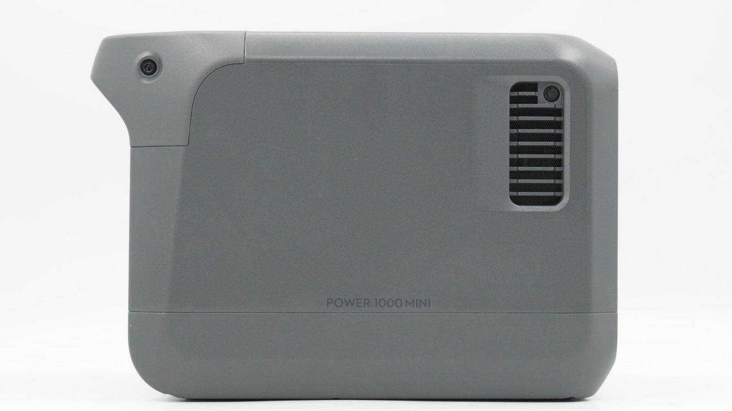
This side of the unit features ventilation holes, with "POWER 1000 MINI" printed on the chassis.
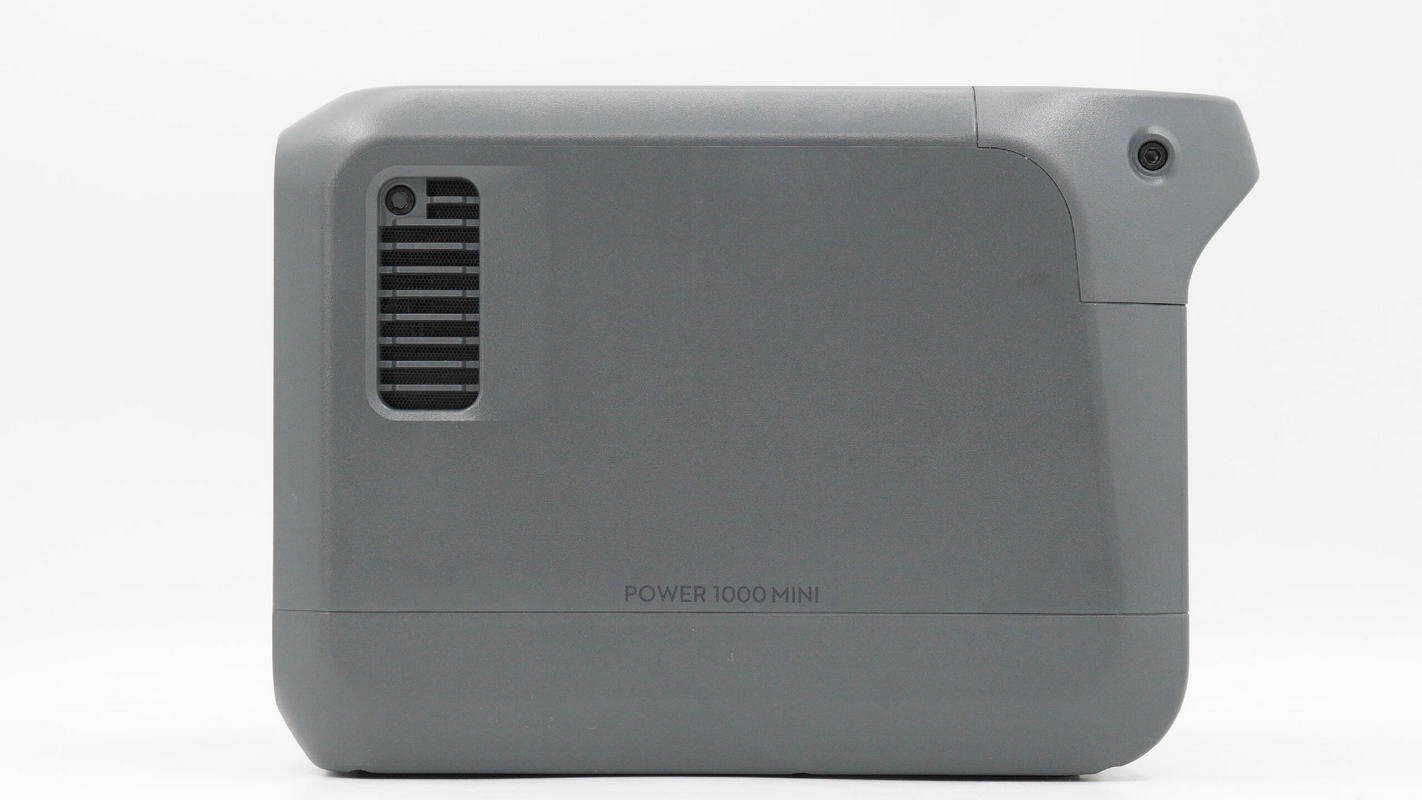
The opposite side has an identical design.
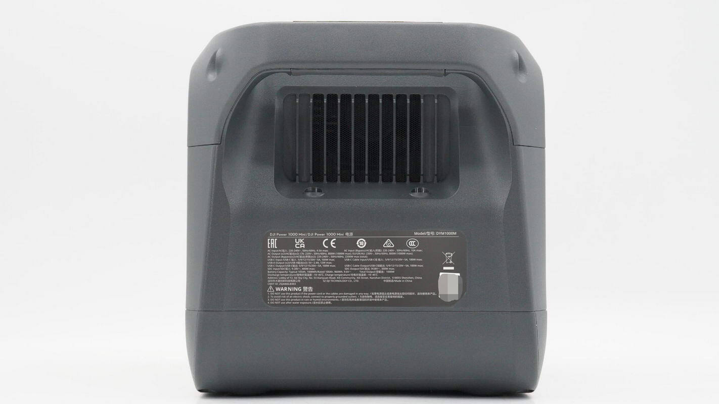
The rear of the unit houses a cooling fan and features a nameplate sticker.
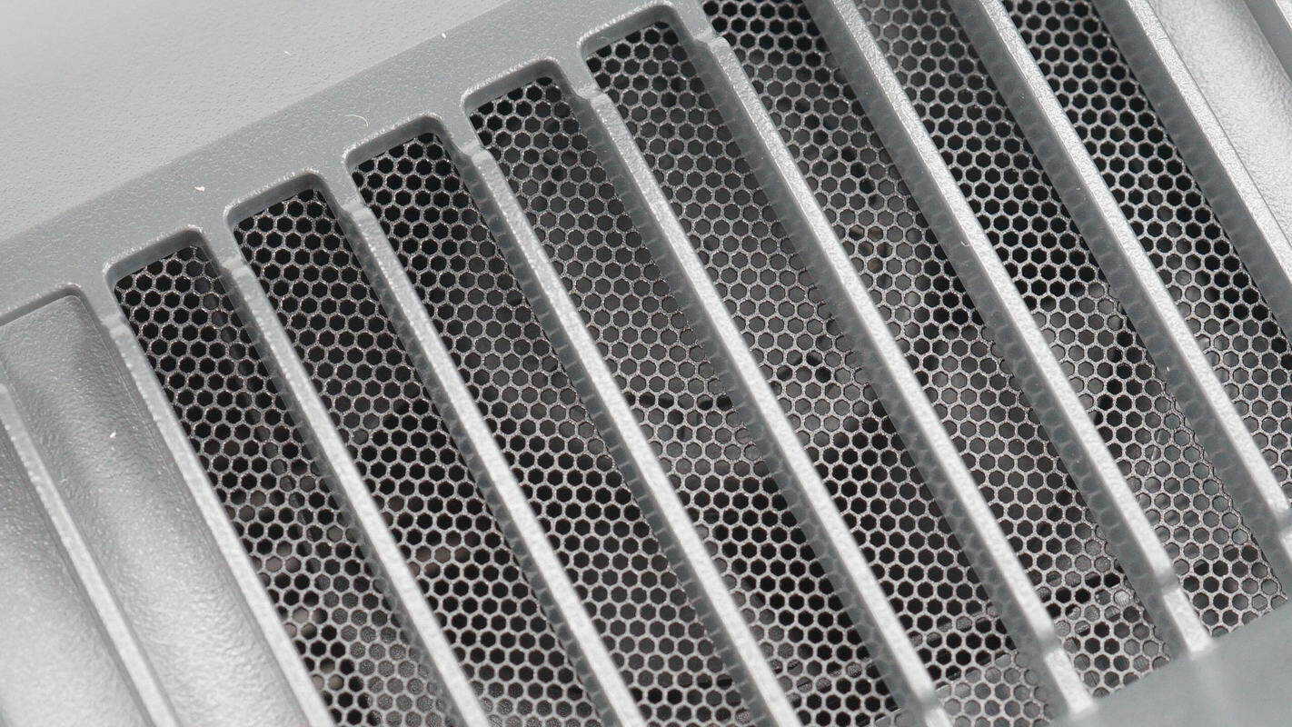
The cooling fan is equipped with a dust filter.
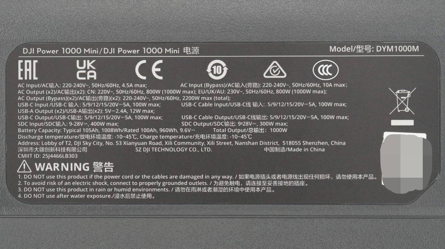
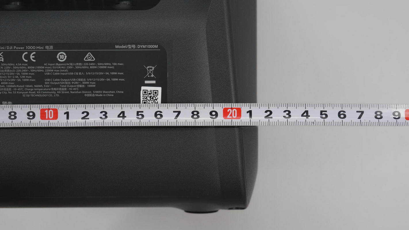
Model: DYM1000M
AC Input: 220–240V~, 50Hz/60Hz, 4.5A max
AC Input (bypass): 220–240V~, 50Hz/60Hz, 10A max
AC Output (x2): CN: 220V~, 50Hz/60Hz, 800W (1000W max); EU/UK/AU: 230V~, 50Hz/60Hz, 800W (1000W max)
AC Output (bypass) (x2): 220–240V~, 50Hz/60Hz, 2200W max (total)
USB-C Input: 5/9/12/15/20V⎓5A, 100W max
USB-C Cable Input: 5/9/12/15/20V⎓5A, 100W max
USB-A Output (x2): 5V⎓2.4A, 12W max
USB-C Output: 5/9/12/15/20V⎓5A, 100W max
USB-C Cable Output: 5/9/12/15/20V⎓5A, 100W max
SDC Input: 9–28V⎓, 400W max
SDC Output: 9–28V⎓, 300W max
Battery Capacity: Typical 105Ah, 1008Wh; Nominal 100Ah, 960Wh, 9.6V⎓
Total Output: 1000W
Discharge Operating Temperature: -10–45℃
Charge Operating Temperature: -10–45℃
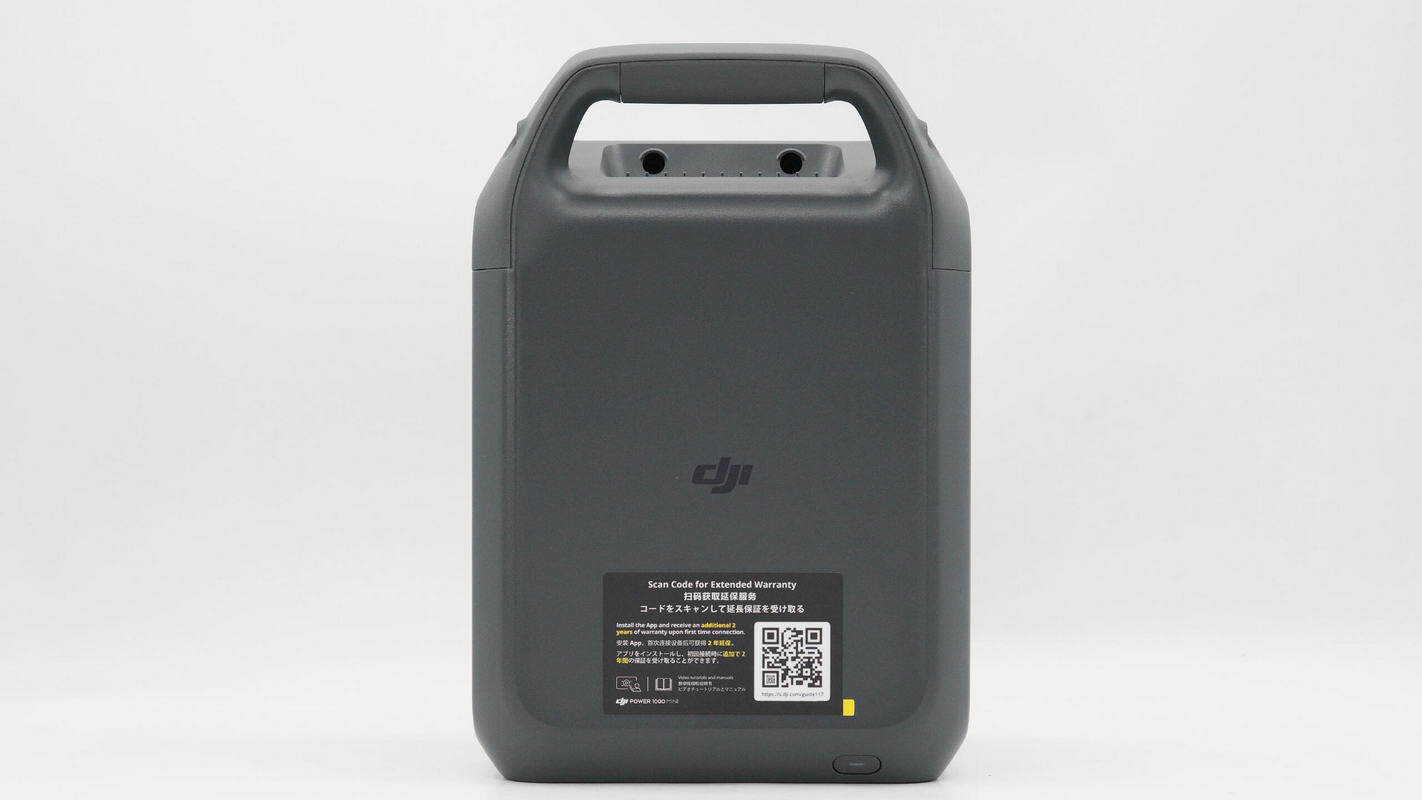
The top of the unit is marked with "DJI," and at the rear, there is an integrated handle with a power switch.
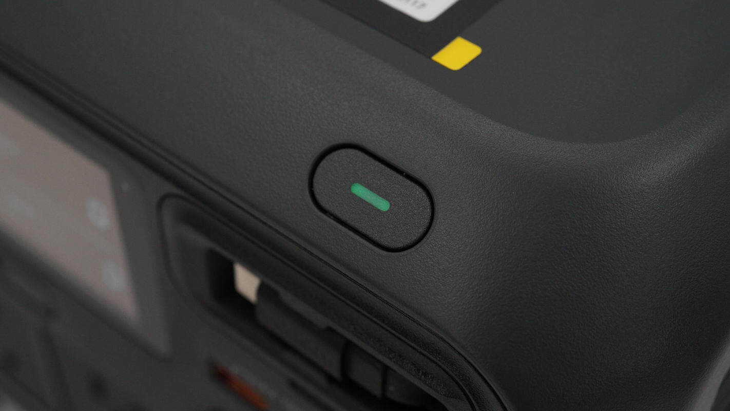
The power switch has an indicator light inside.
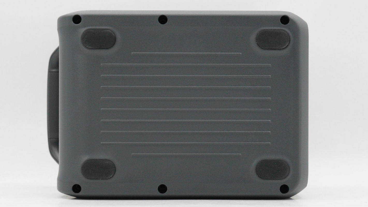
The bottom is equipped with non-slip feet.
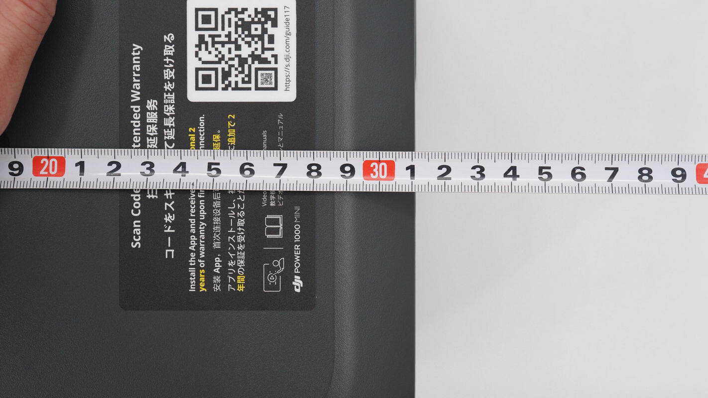
The length of the unit is about 310 mm (12.2 inches).

The length of the unit’s bottom is about 285 mm (11.22 inches).
The width of the unit is about 214 mm (8.43 inches).

The height of the unit is approximately 215 mm (8.46 inches).

The weight is about 11.35 kg (25.022 pounds).
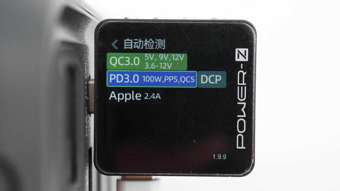
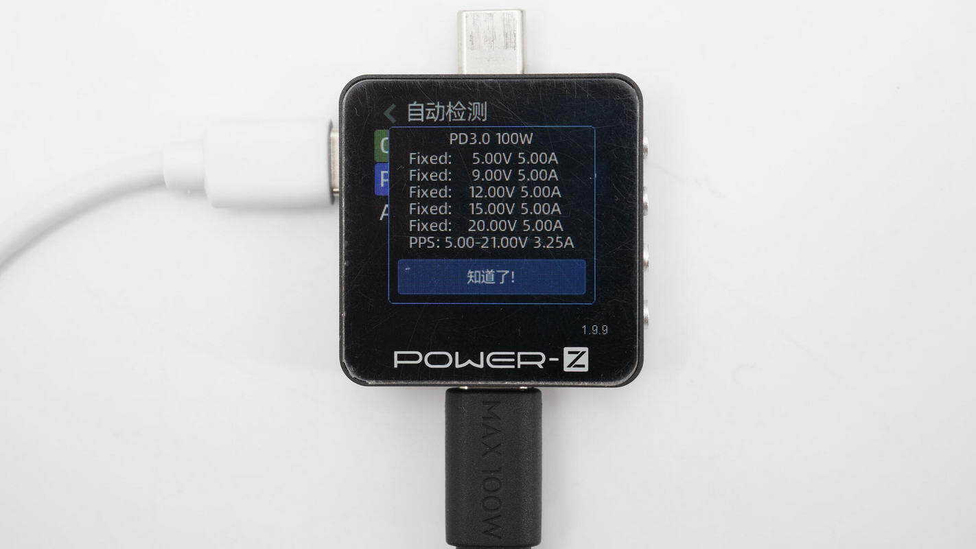
ChargerLAB POWER-Z KM003C shows that the USB-C supports QC3.0/5, PD3.0, PPS, DCP, and Apple 2.4A protocols.
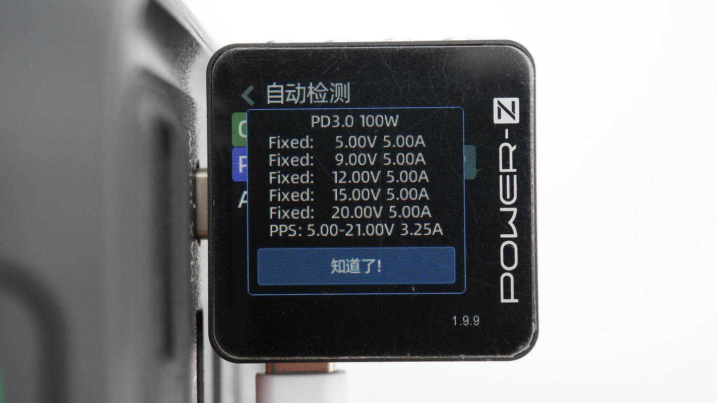
It supports five fixed PDOs of 5V5A, 9V5A, 12V5A, 15V5A, and 20V5A. It also supports a set of PPS, which is 5-21V 3.25A.
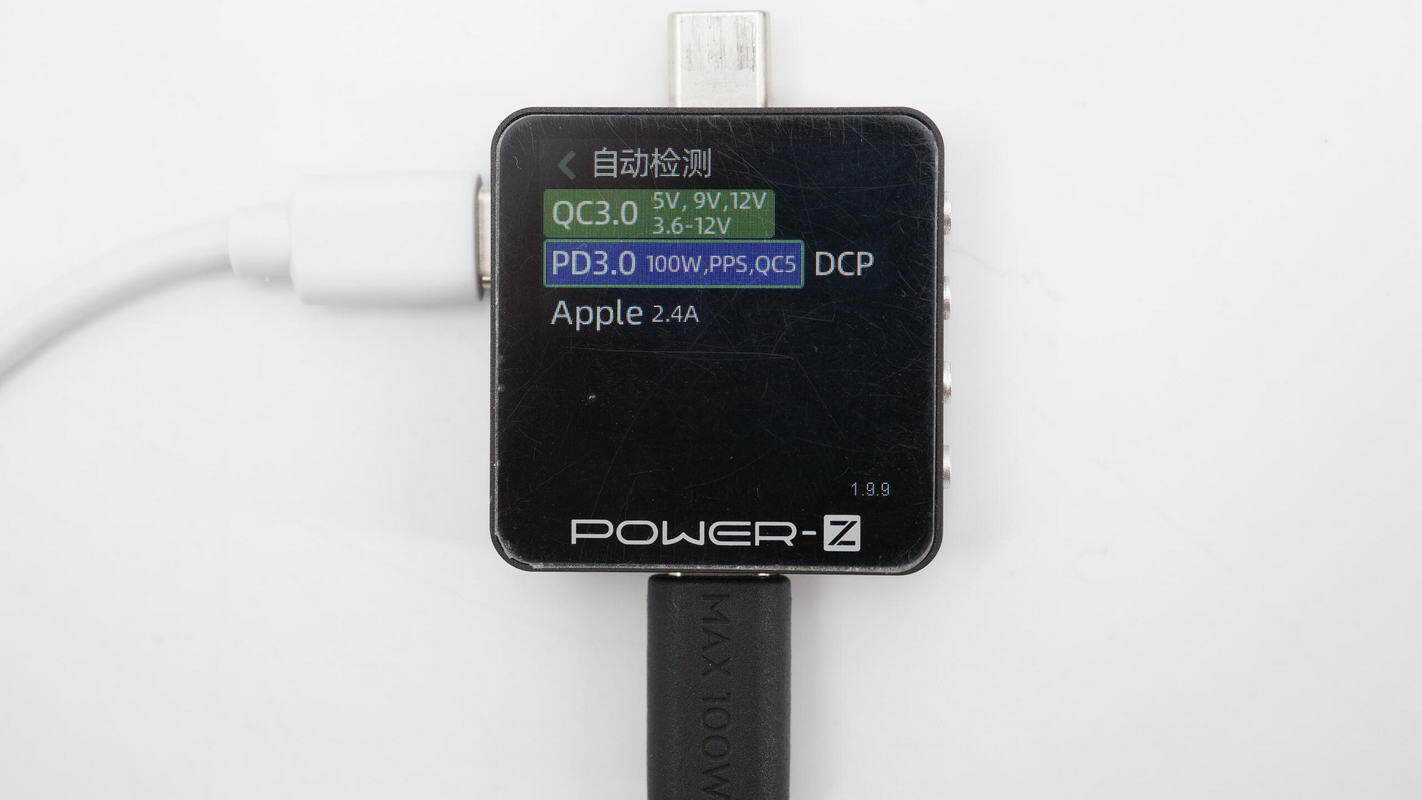
The retractable USB-C cable supports the same protocols as the USB-C port.
The PDO messages are also the same.
The USB-A ports do not support fast-charging protocols.
Teardown
Next, let's take it apart to see its internal components and structure.
Remove the cover of the retractable USB-C cable module.
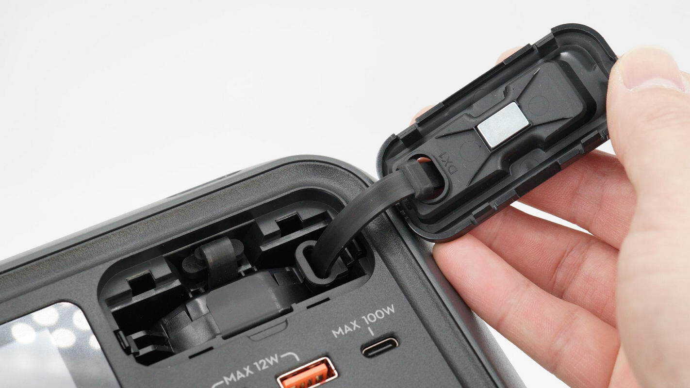
Beneath the cover is the retractable cable module, and the back of the cover is equipped with a magnet.
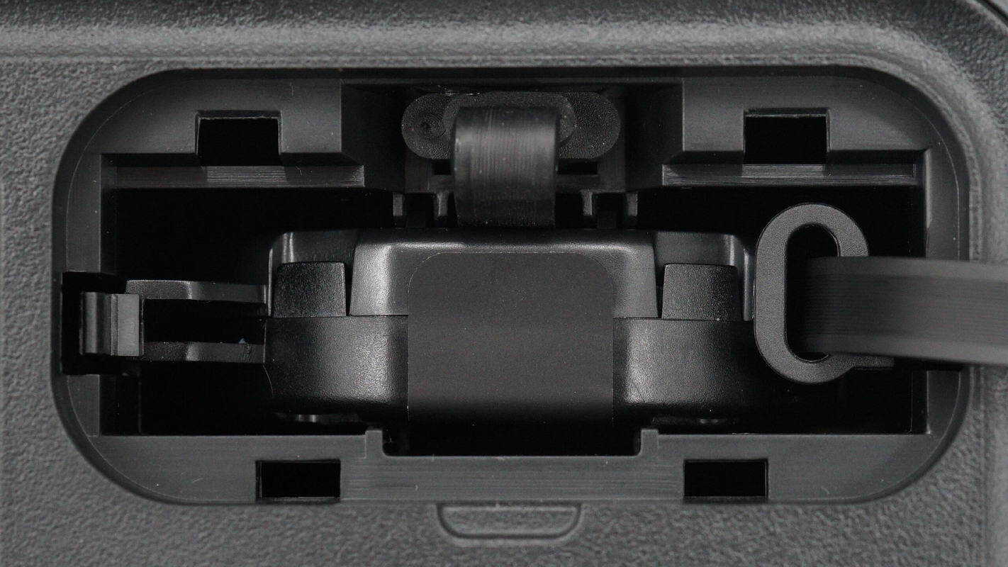
The retractable cable module is secured on both sides with clips, and a USB-C port is located on the top.
Remove the retractable cable module.
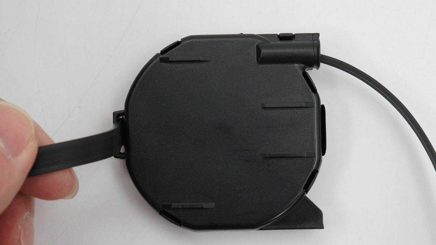
One side of the module features positioning protrusions.
The opposite side has a carbon brush.
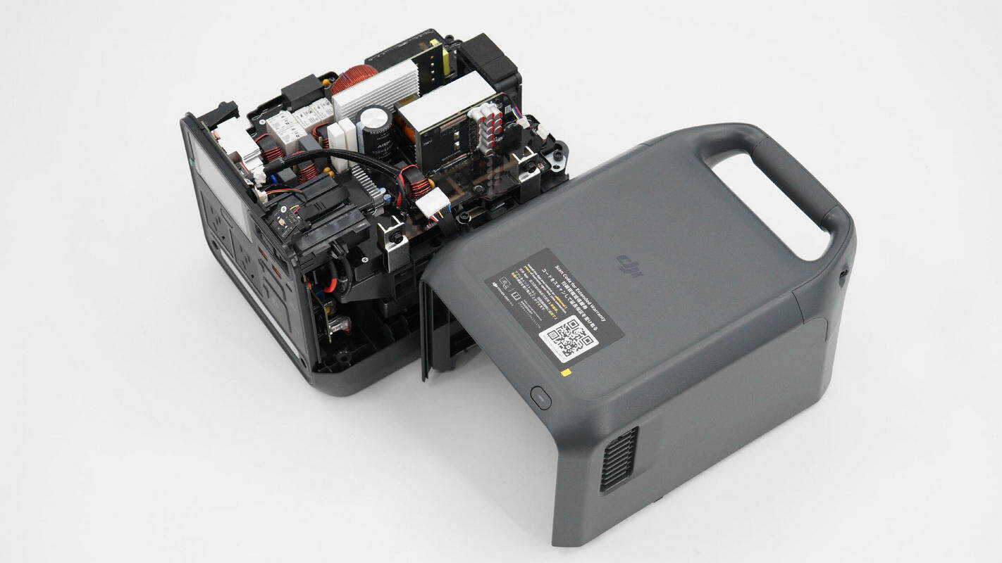
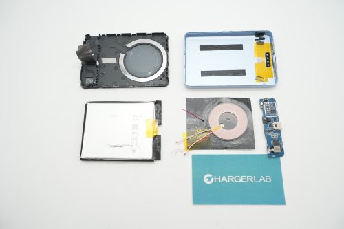
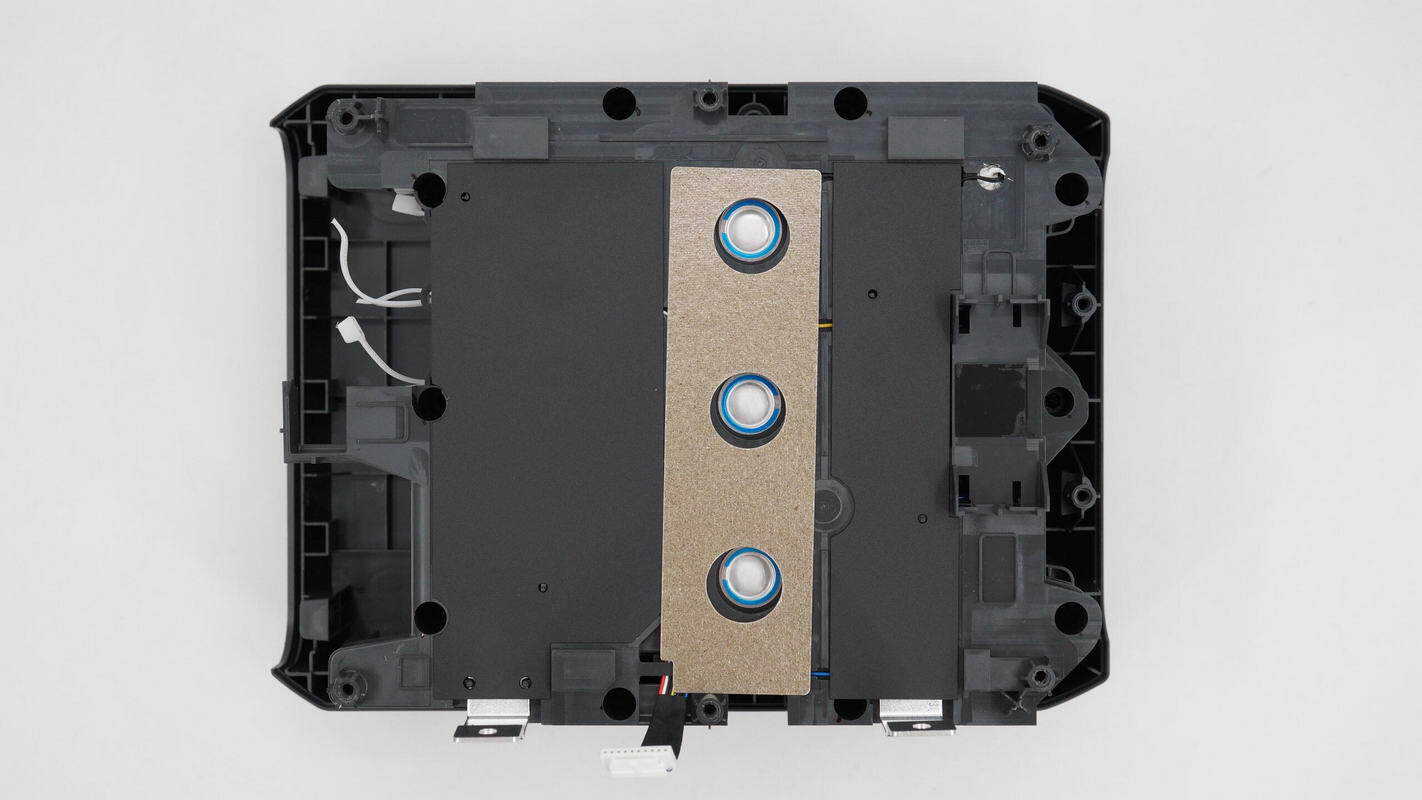
Unscrew the screws at the bottom to remove the outer casing of the power station.
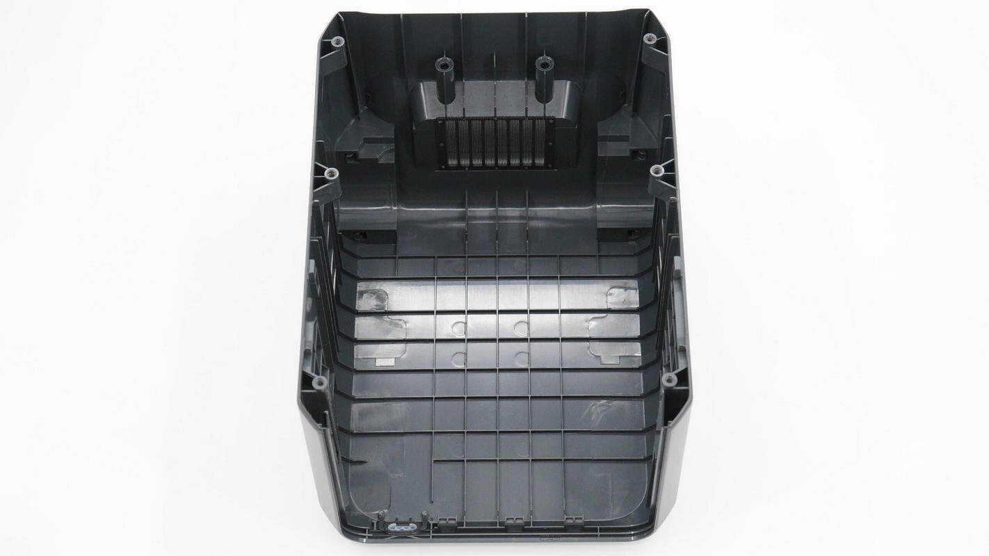
Inside the casing, there are reinforcing ribs.
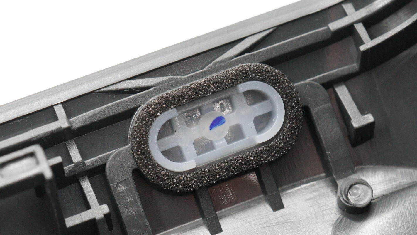
The power button is covered with foam for light shielding.

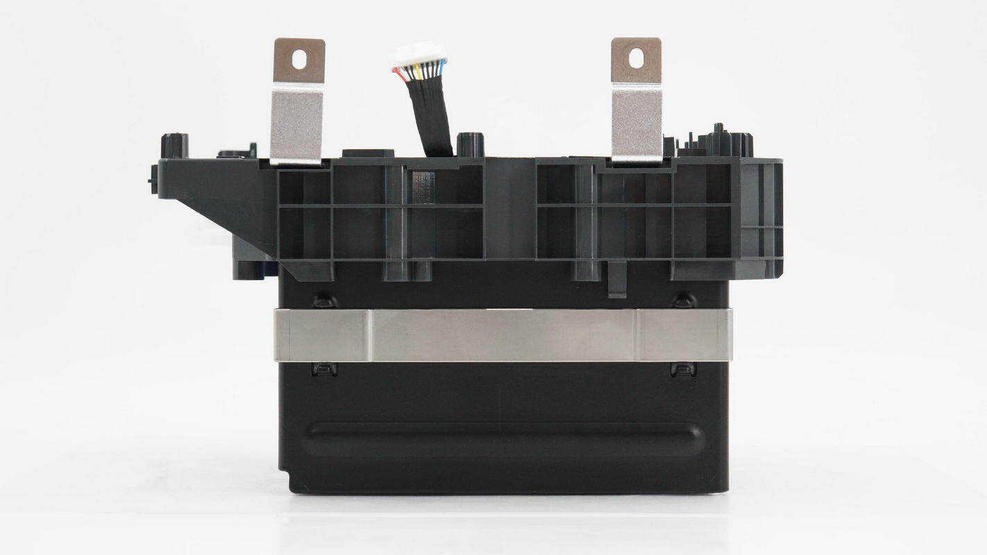
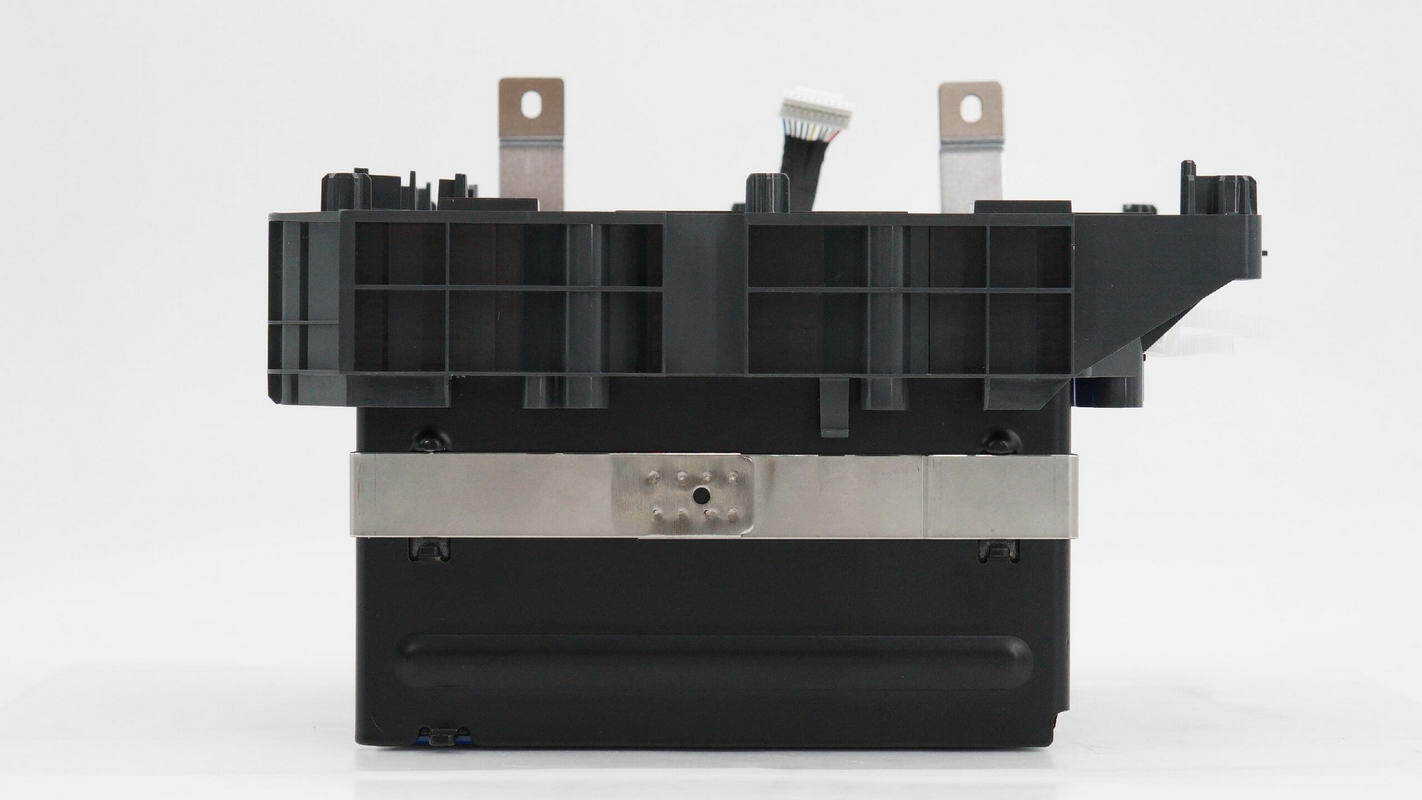
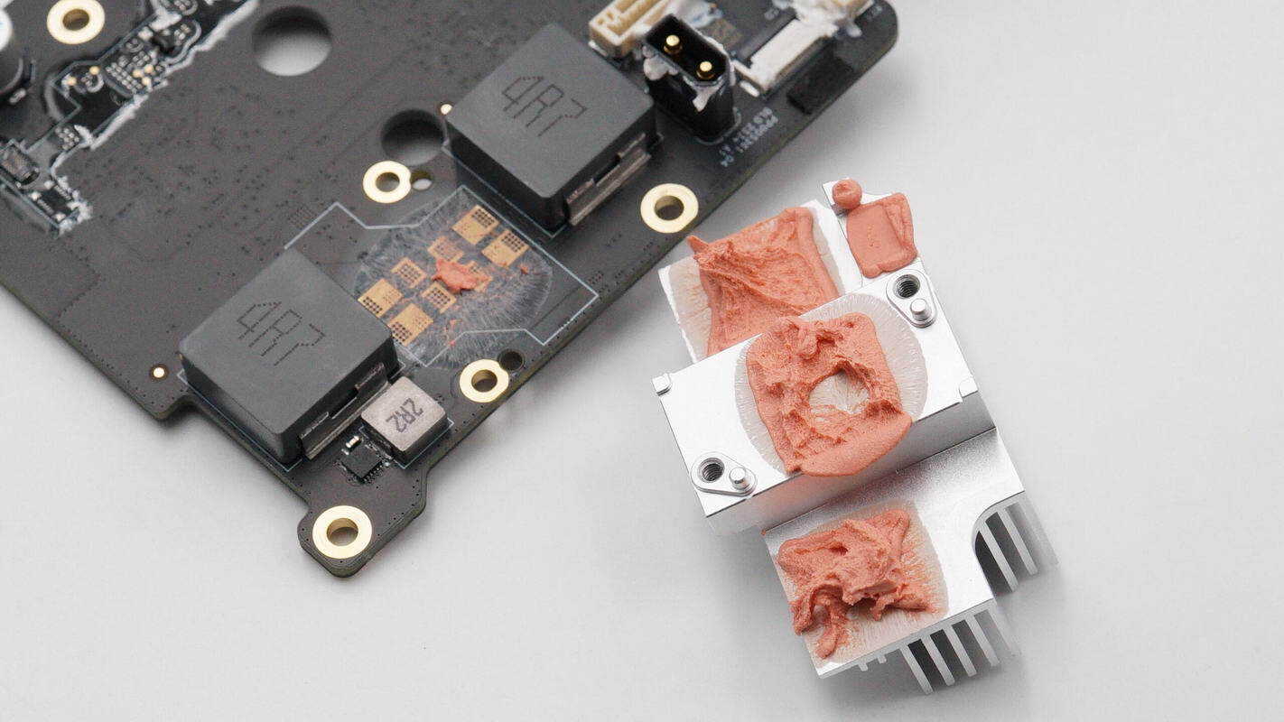
Inside, there is a bidirectional inverter module secured with screws.
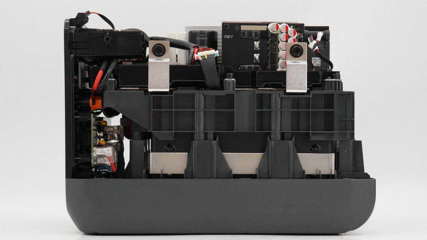
Beneath the bidirectional inverter module is the battery pack, covered by a plastic panel. The battery terminals are connected to the bidirectional inverter module.
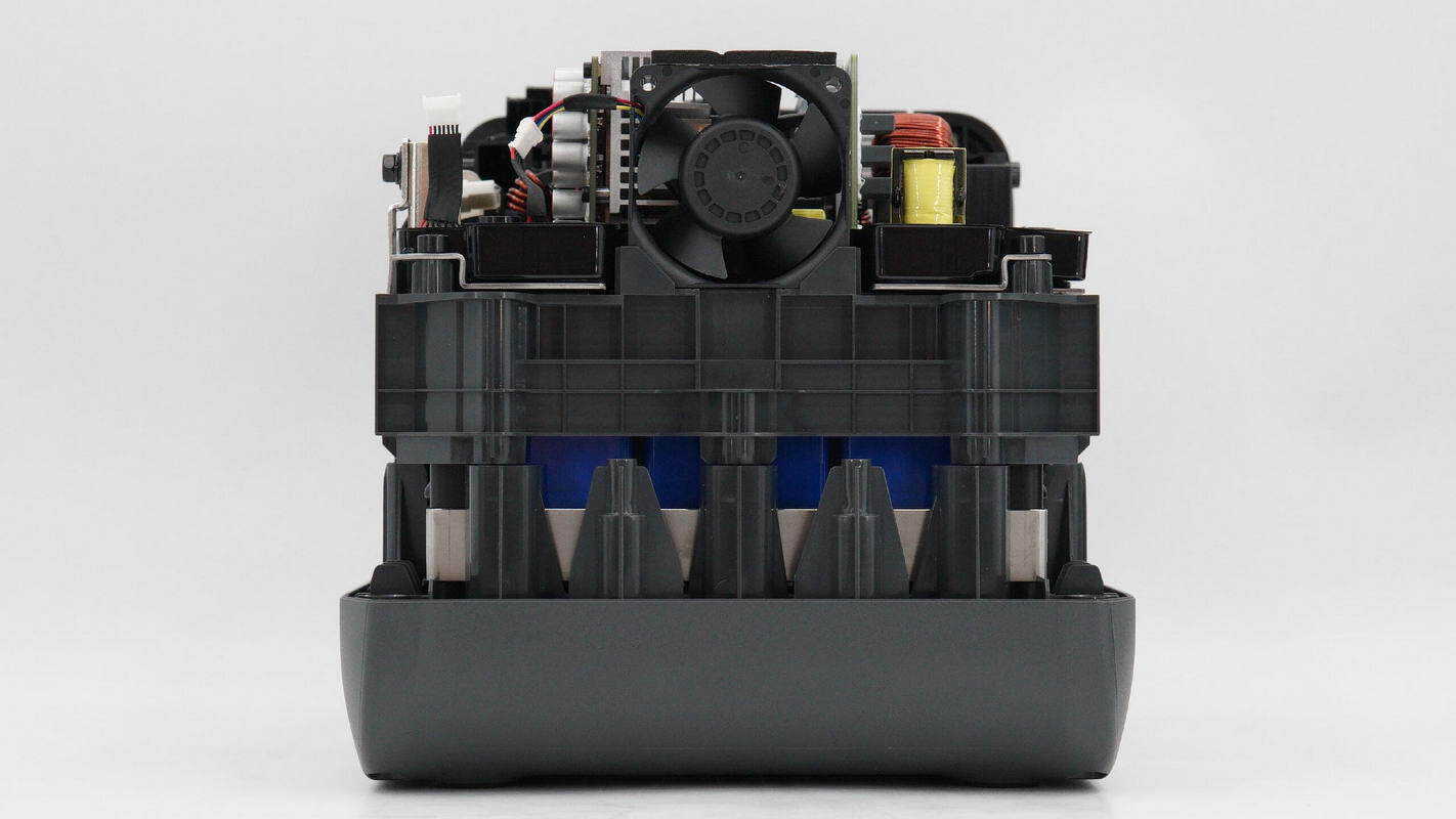
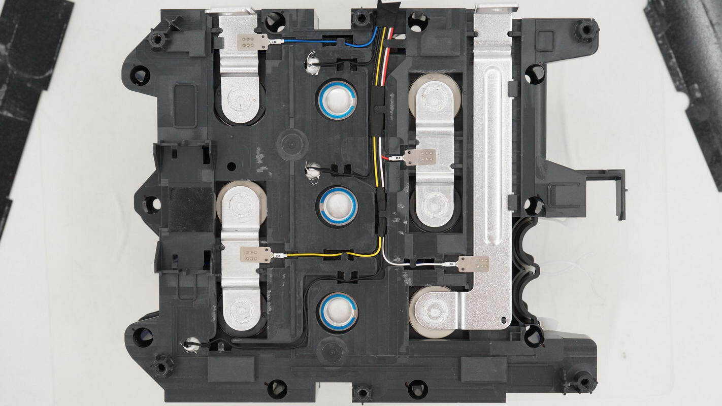
A cooling fan is installed on the opposite side.
The battery pack cover on the opposite side is also secured with screws.
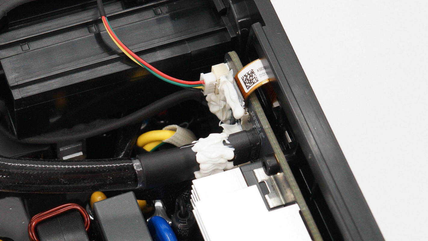
The side panel is equipped with wiring for the power switch, the display ribbon cable, and a power connector.
Close-up of the battery pack’s positive and negative terminals and the thermistor sensing wires.

The cooling fan is model CHT6012BM-W25C, rated at 12V 0.3A, and made in China.
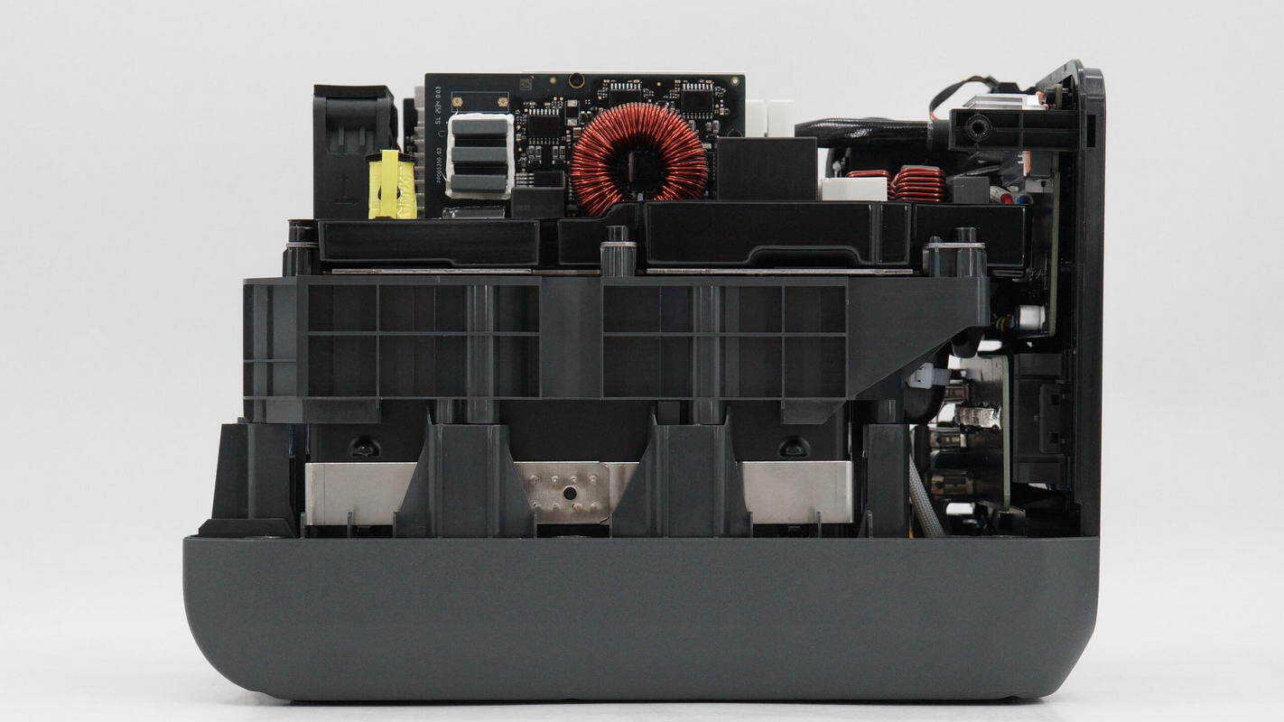
Remove the bidirectional inverter module.
Both the AC input and AC output cables are equipped with ferrite cores to suppress high-frequency interference.

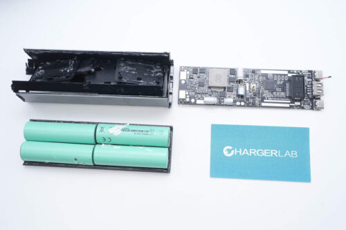
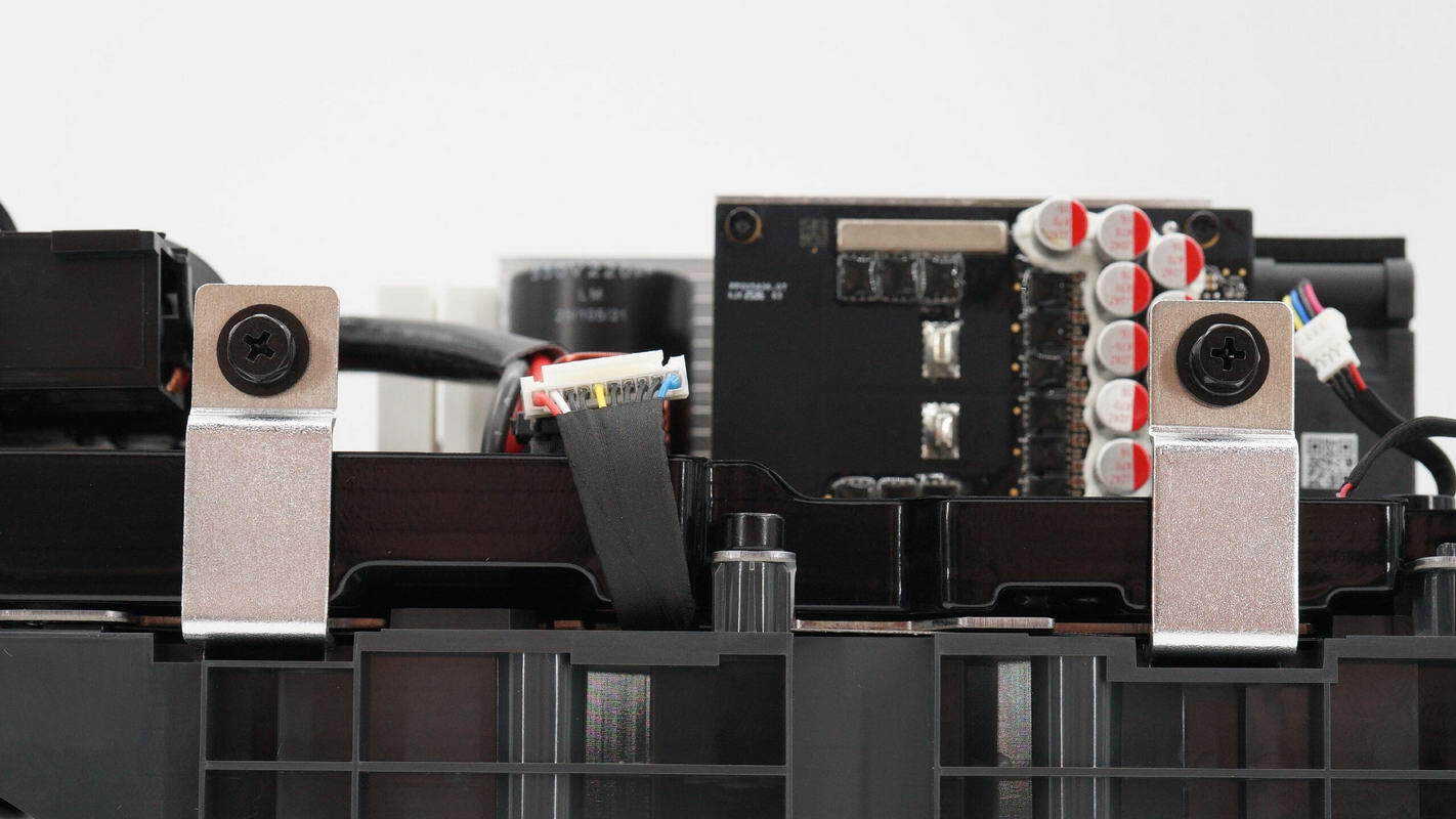
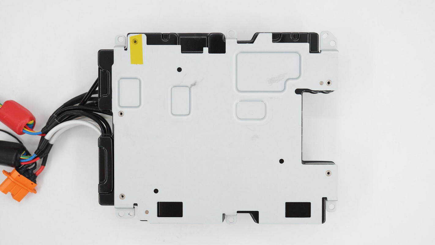
Remove the side panel along with the bidirectional inverter module.
Remove the battery pack, which is insulated with Mylar and mica sheets.
Inside the insulation frame, three thermistors correspond to three battery series, each with its respective voltage detection wire.
The battery pack is strapped with a steel band, with iron plates on both sides for protection.
The steel strap is secured by spot welding.
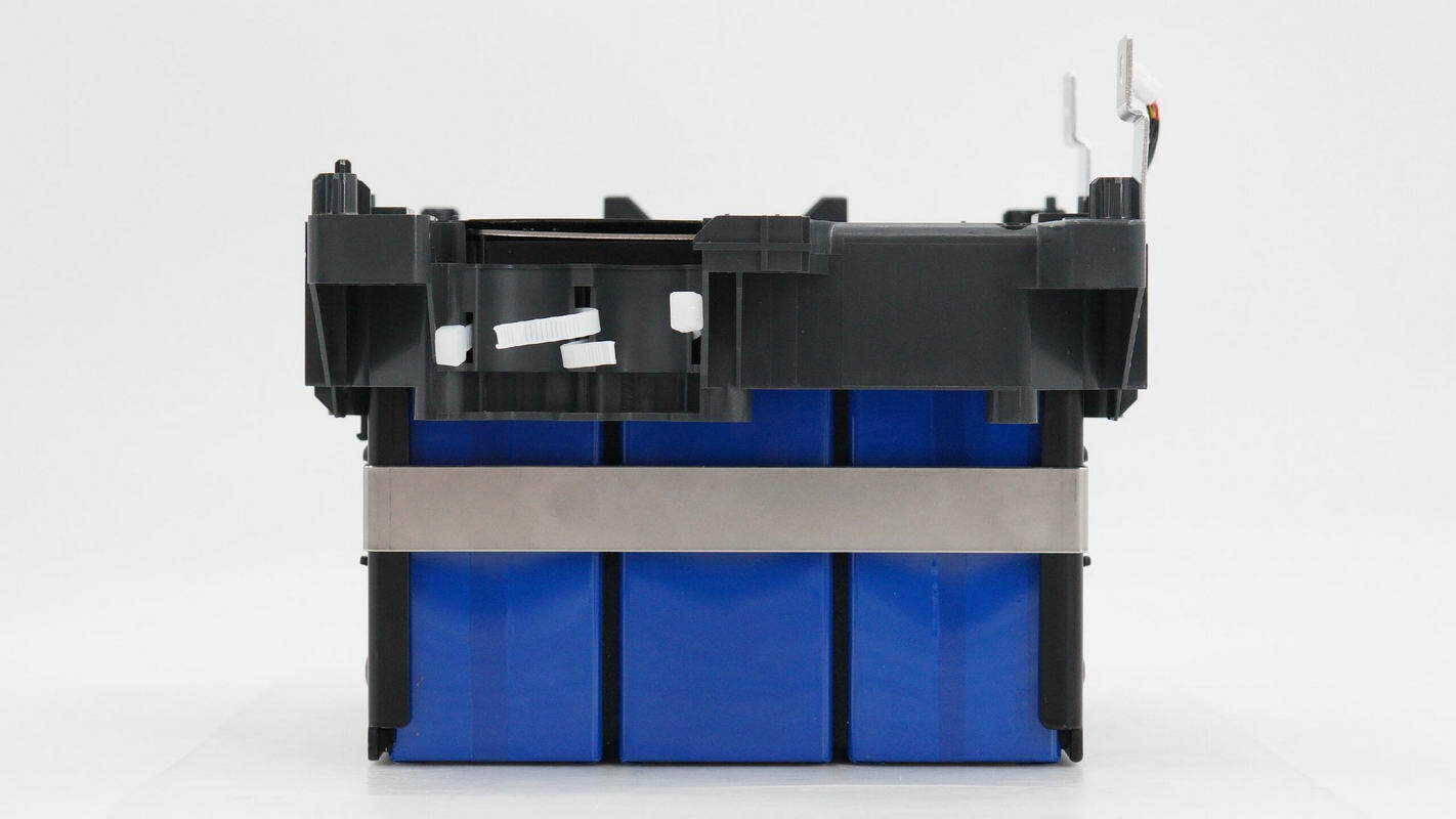
The batteries are prismatic lithium iron phosphate cells, encased in blue heat-shrink sleeves.
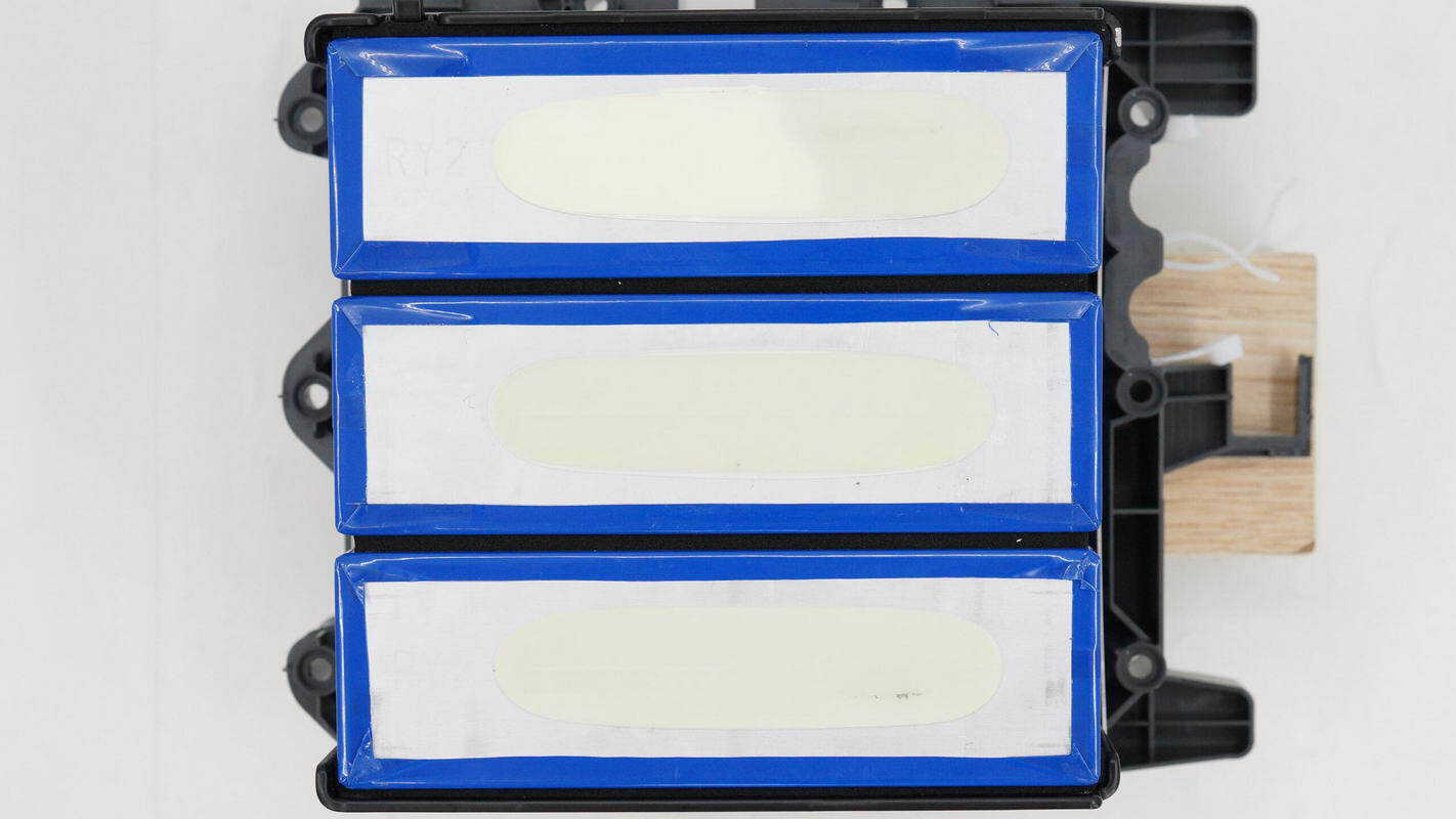
The bottom of the battery cells is secured with adhesive.
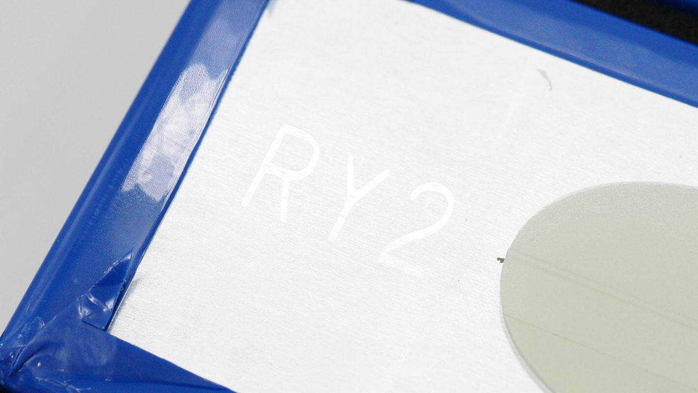
The bottom is marked with the characters "RY2."

The height is about 115 mm (4.53 inches).
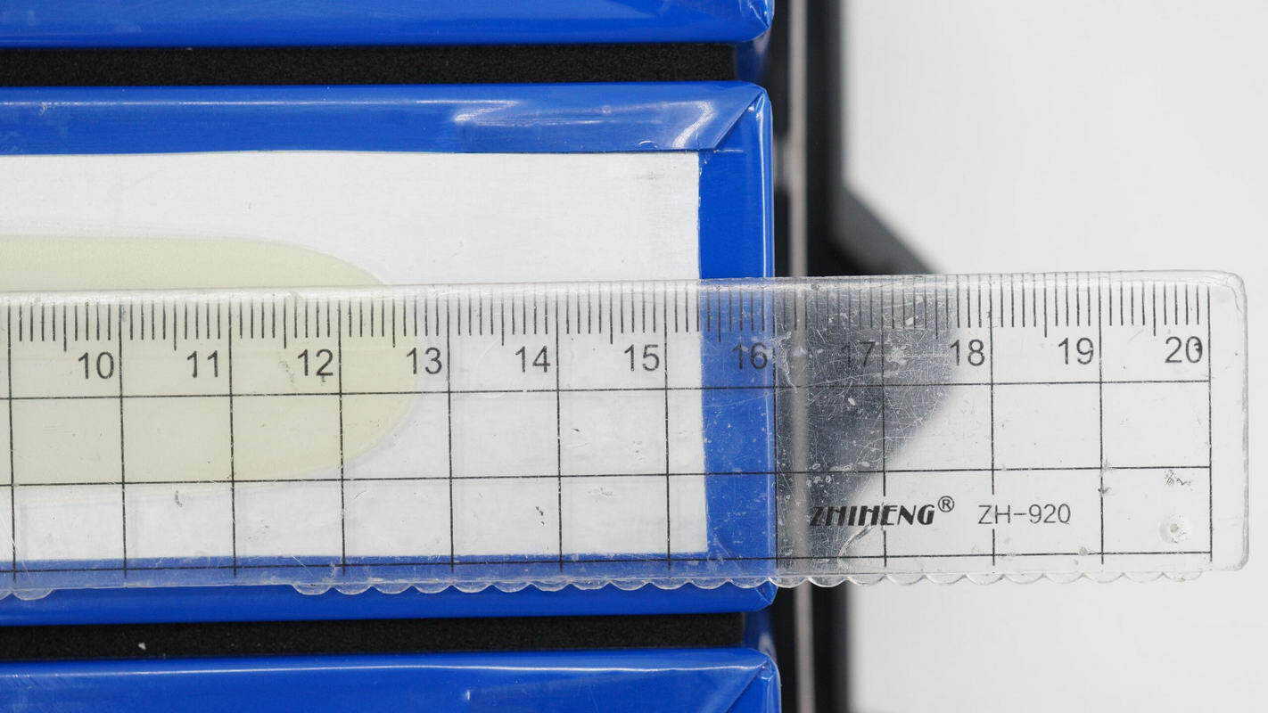
The width is about 160 mm (6.3 inches).
The thickness is about 50 mm (1.97 inches).

Close-up of the battery spot-welded connections.
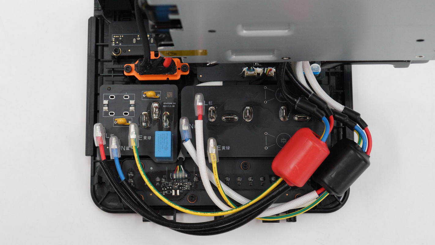
The wires of the bidirectional inverter module are connected via plug connectors.
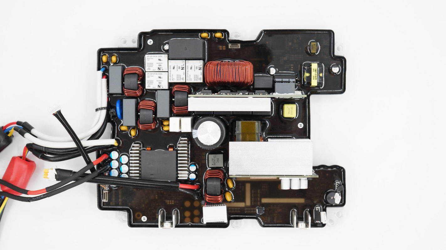
The bidirectional inverter module is equipped with inverter output wires, AC input wires, SDC interface wiring, safety X2 capacitors, common mode chokes, switching relays, a PFC inductor, and filter capacitors, among other components.
The metal plate on the back is used for mounting and securing the module.
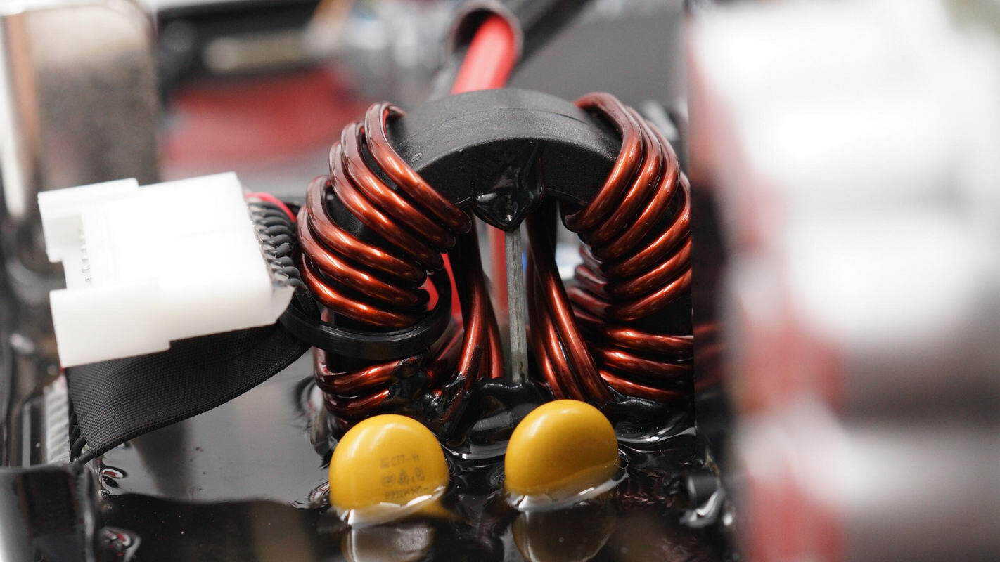
The DC input terminals are equipped with a common mode choke.
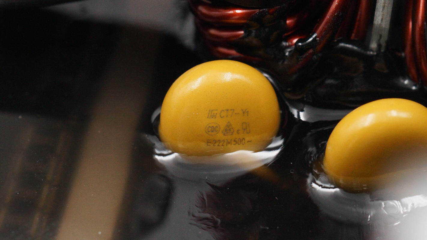
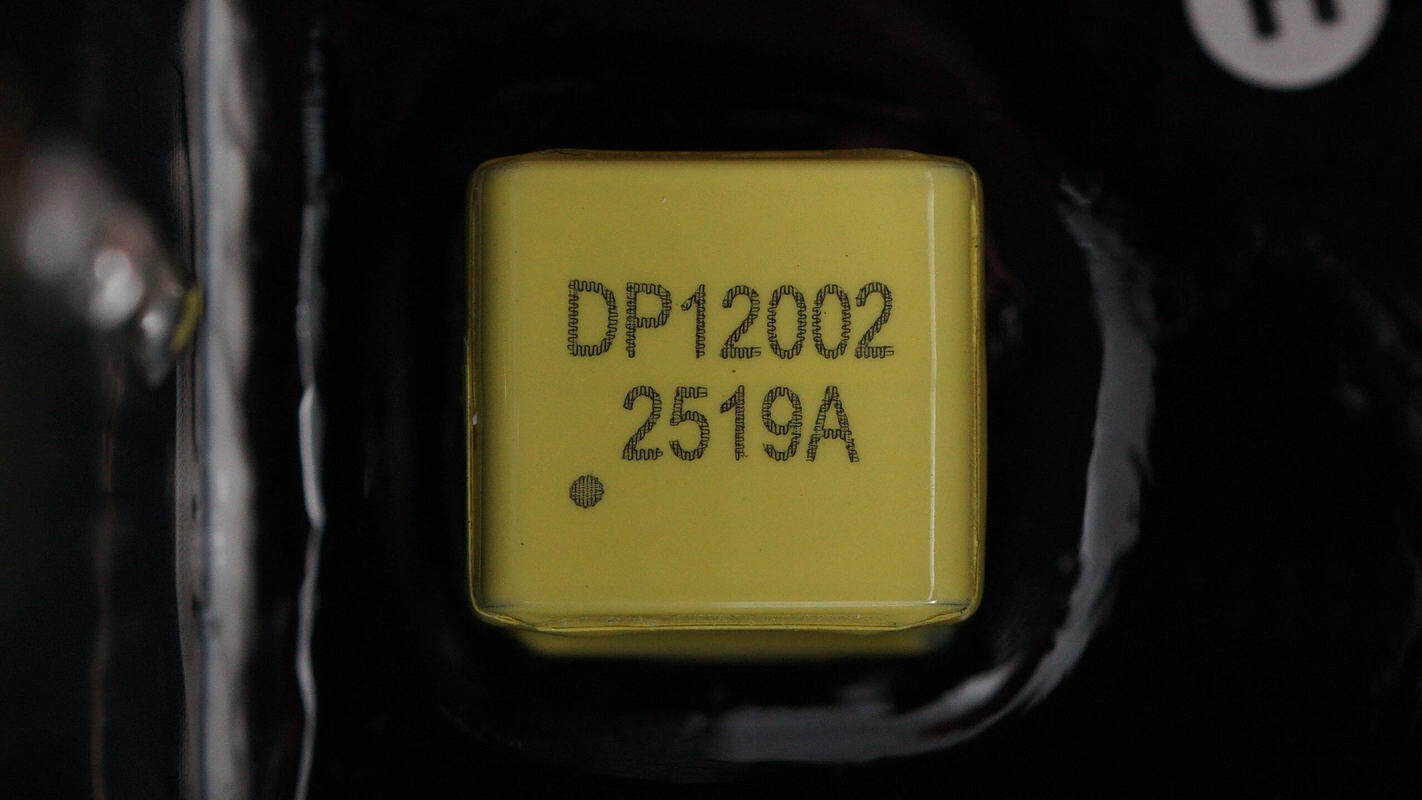
The yellow Y-capacitor is from FNR, with the part number E222M.
The small PCB on the low-voltage side features boost MOSFETs, solid capacitors, and drivers.
The solid capacitors are rated at 470 μF, 16 V.
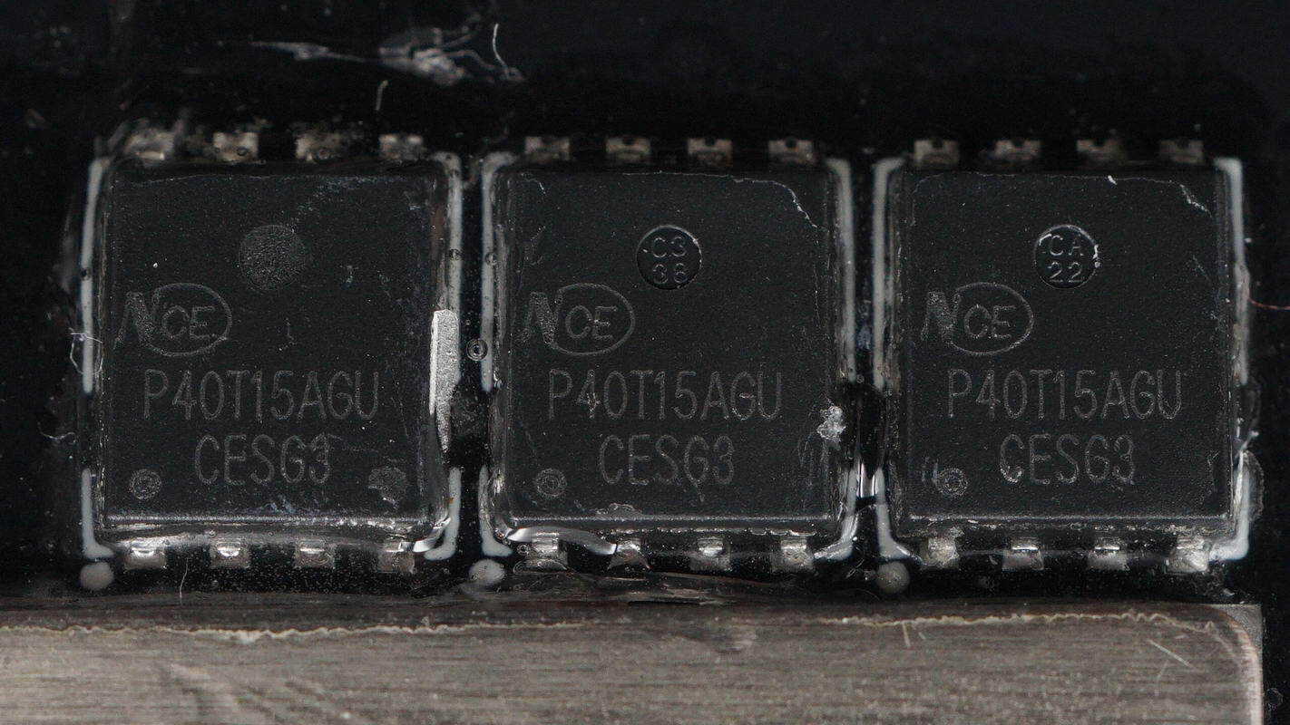
The boost MOSFETs are from NCE, model NCEP40T15AGU, NMOS type, rated at 40 V with an on-resistance of 1.2 mΩ, in a DFN 5×6 package, with a total of 12 units.

Two drivers are from SGMICRO, model SGM48211. Each is a 120 V half-bridge driver with fully independent high-side and low-side channels. The chip supports a peak current of 4 A, integrates bootstrap diodes, and comes in a TDFN 4×4 package.
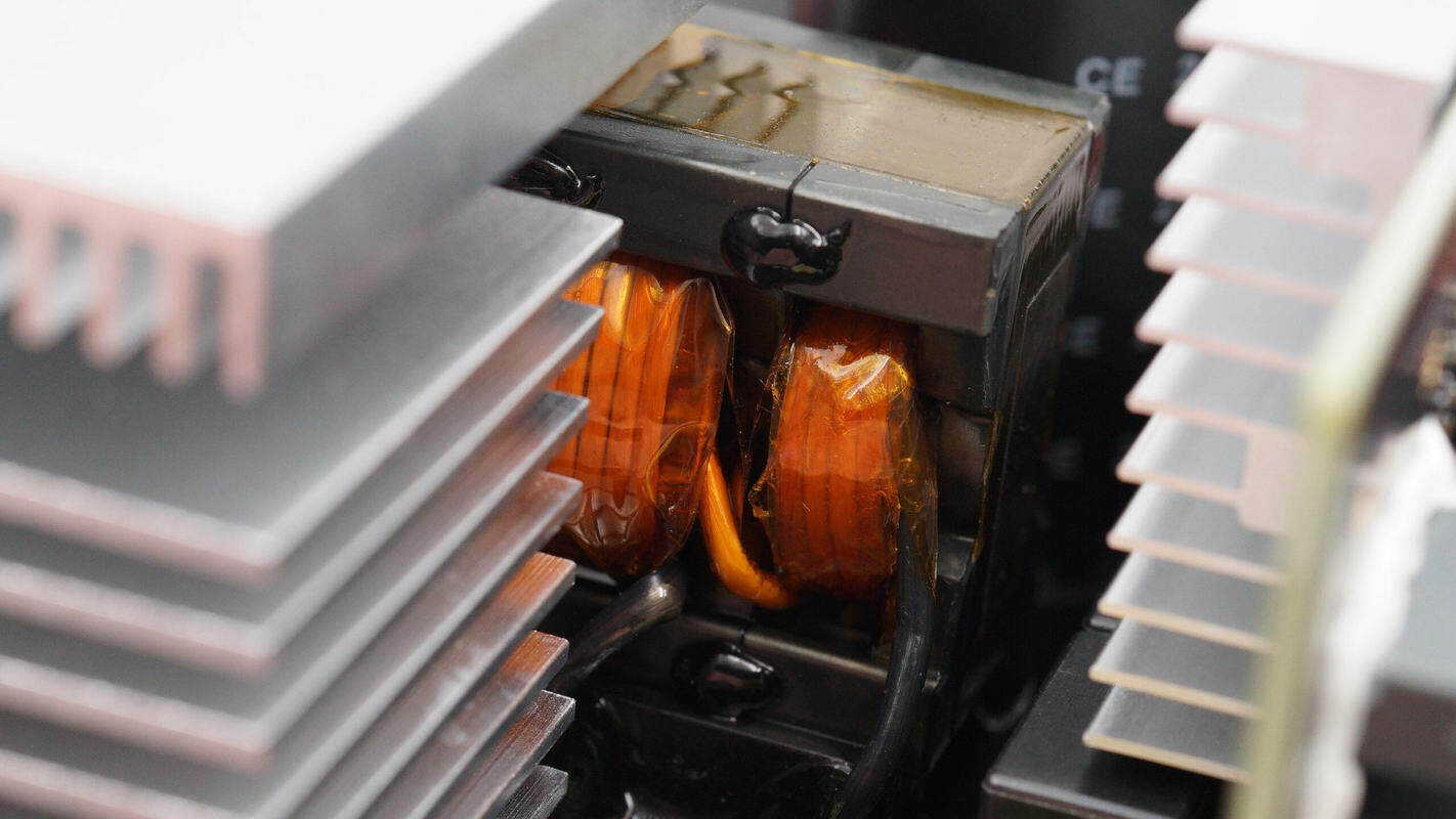
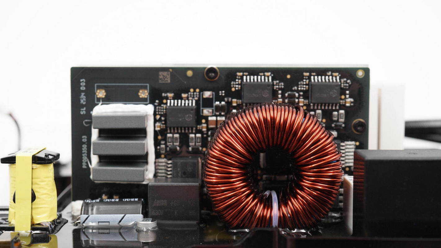
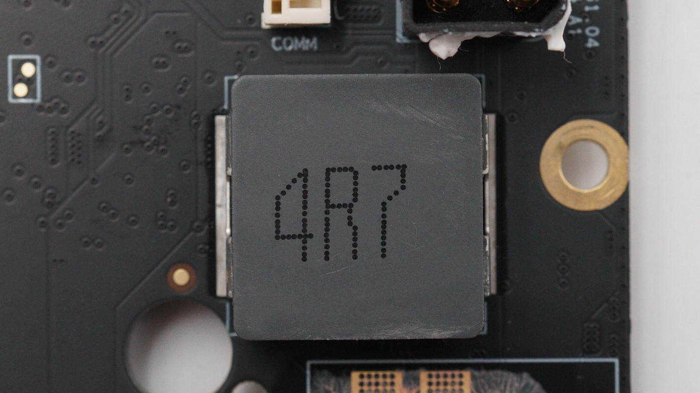
The boost transformer is wound with Litz wire.
There are four film capacitors mounted on the side of the transformer.

The capacitors are rated at 630 V, 1 μF.
Close-up of the current transformer.
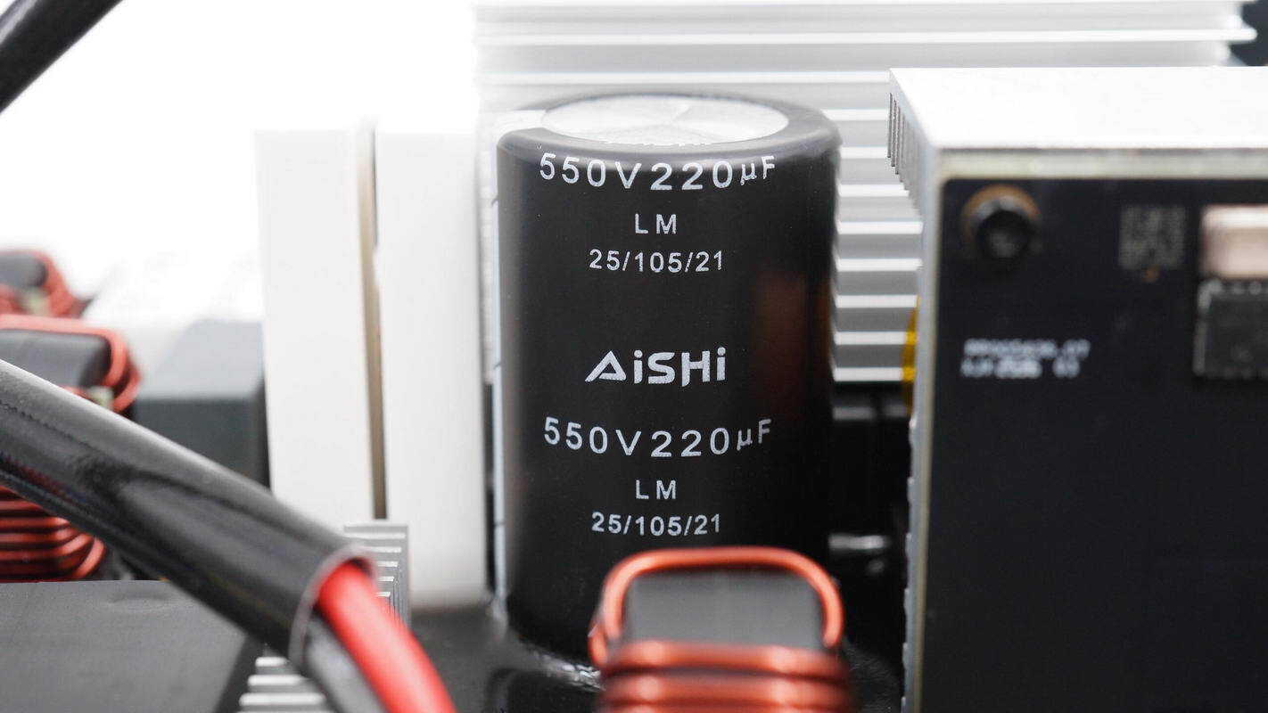
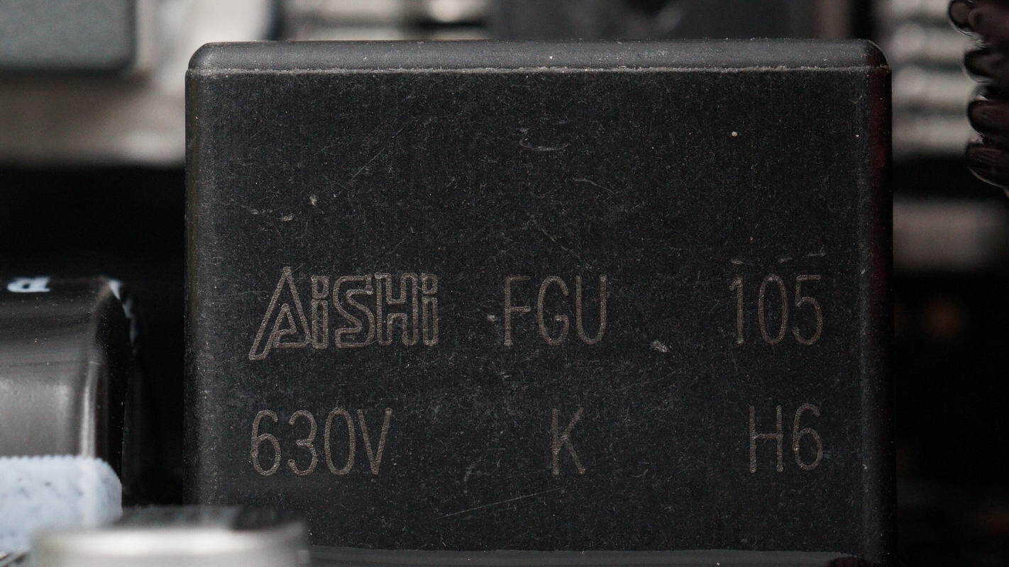
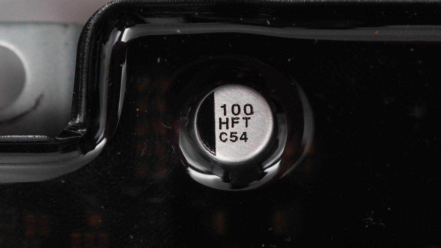
The high-voltage filter capacitor is from AiSHi, part of the LM series of long-life electrolytic capacitors, rated at 550 V, 220 μF.
On the opposite side, there is a small high-voltage PCB.
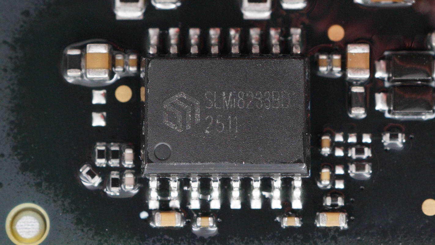
The isolated driver is from SiLLUMIN, model SLMi8233BD. It is an isolated driver with 5 kVRMS isolation capability and a peak output current of 4 A. The chip features an internal isolation voltage of 1500 V between the two drivers, supports 40 V input voltage, and operates at 3–18 V. It comes in an SOP16W package.
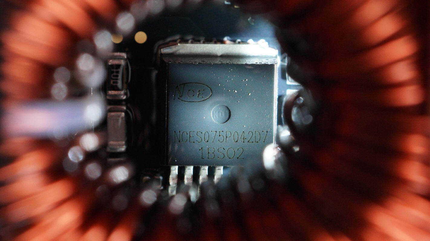
The high-voltage MOSFET is from NCE, model NCES75P042D7. It is a silicon carbide MOSFET, rated at 750 V with an on-resistance of 42 mΩ, in a TO263-7L package.
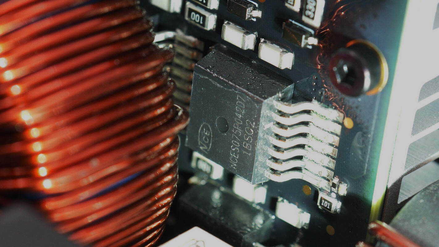
The other MOSFET has the same model.
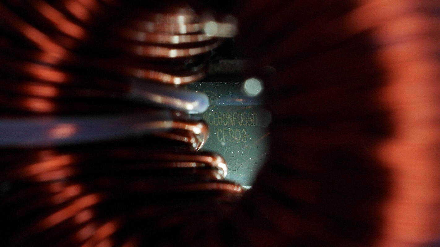
This MOSFET is from NCE, model NCE60NF055D. It is an NMOS, rated at 650 V with an on-resistance of 50 mΩ, in a TO-263 package.
The three resonant capacitors are reinforced with adhesive.

Close-up of the PFC boost inductor.
The film capacitor is rated at 630 V, 1 μF.

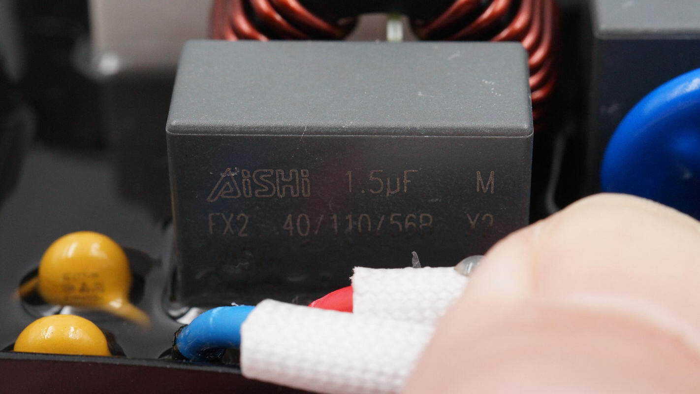
The safety X2 capacitor is from AiSHi, with a rating of 3.5 μF.
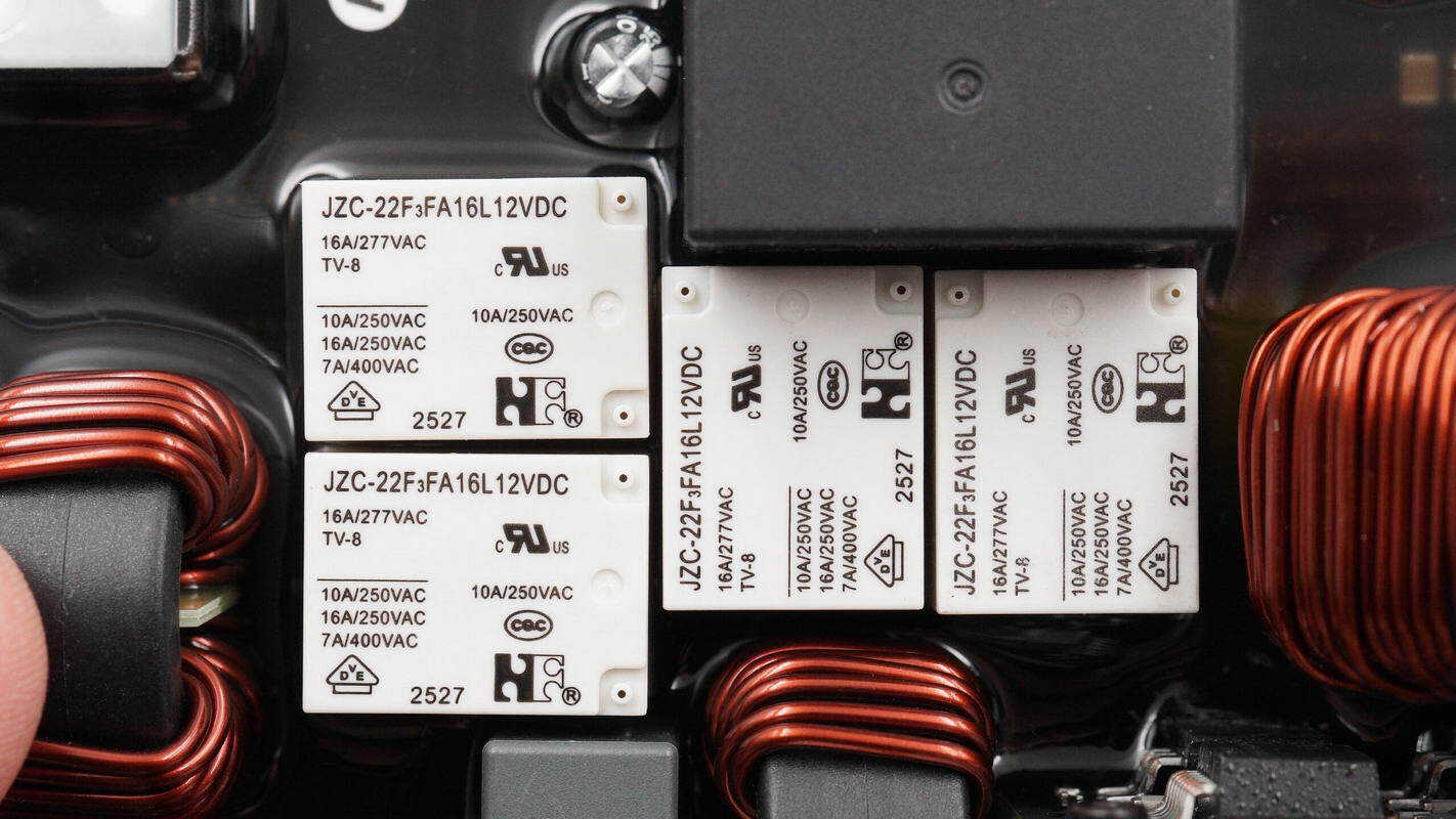
The switching relays are from Forward Relay, model JZC-22F3FA16L12VDC. Each relay has a single normally open contact, with a contact rating of 16 A/250 VAC and a coil voltage of 12 V.
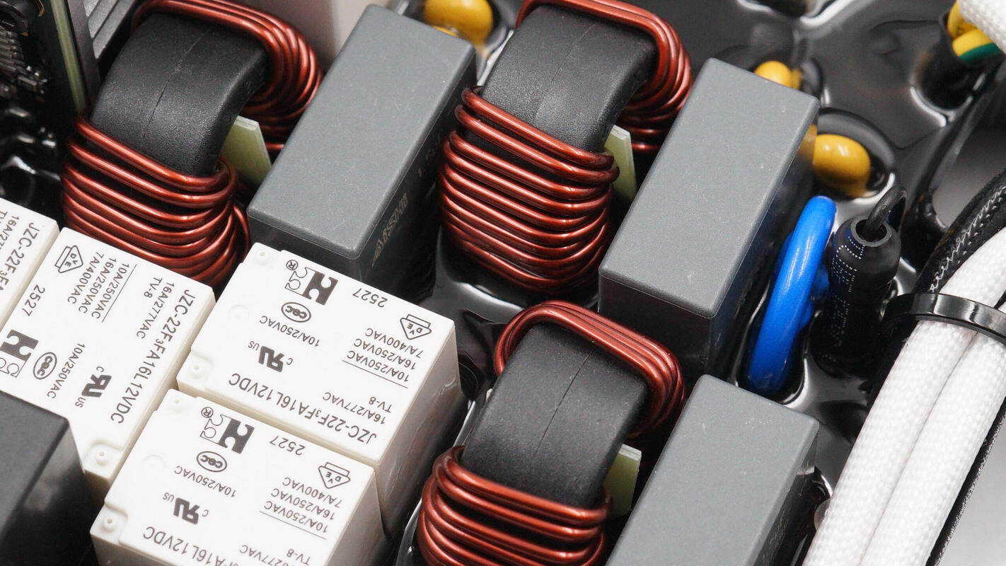
The common mode chokes and safety-rated X2 capacitors are arranged alternately. The common mode chokes are wound with enameled wire and feature a built-in Bakelite insulation board.
The safety X2 capacitors are rated at 1.5 μF.
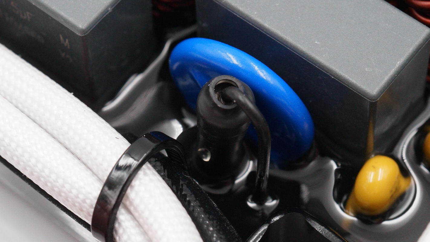
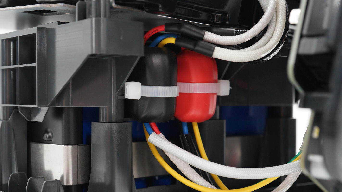
Close-up of the varistor and fuse, with the fuse insulated by a heat-shrink tube.
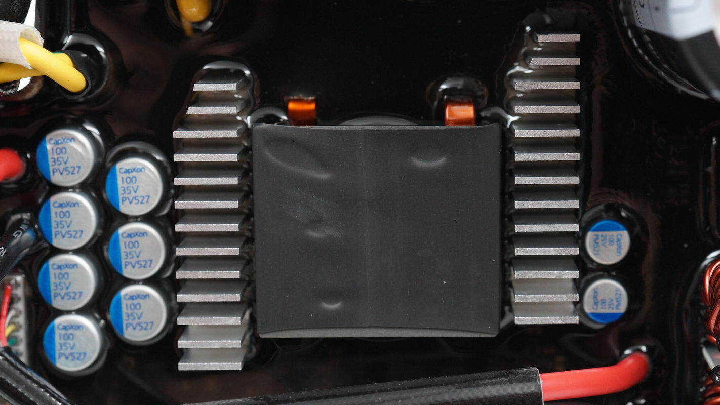
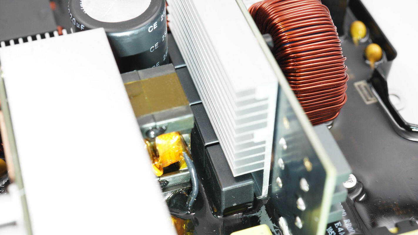
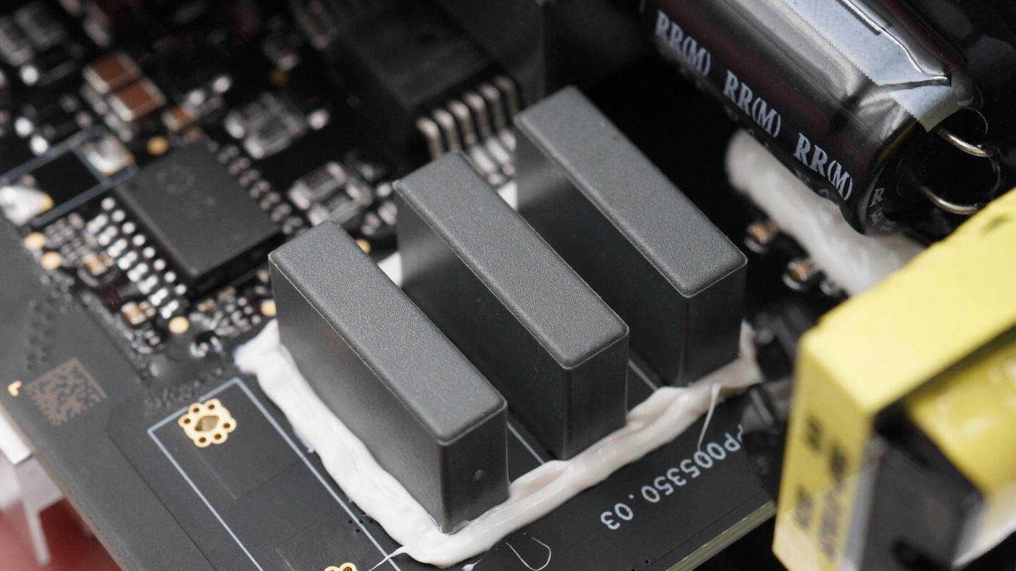
The inductor used for powering the SDC interface is wound with copper tape, and on both sides, there are heatsinks for filter capacitors and MOSFETs.
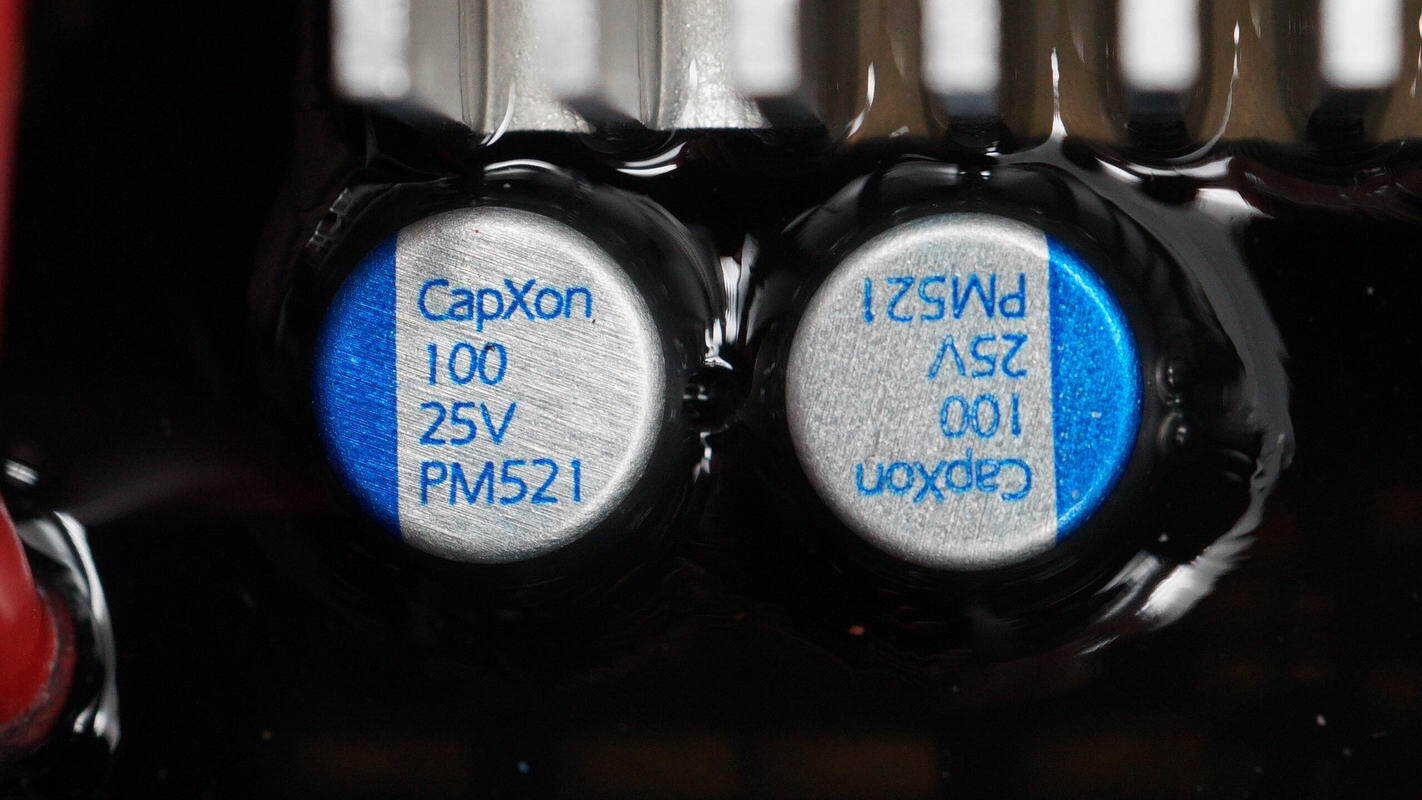
The solid capacitors are from CapXon, with a rating of 100 μF, 25 V.
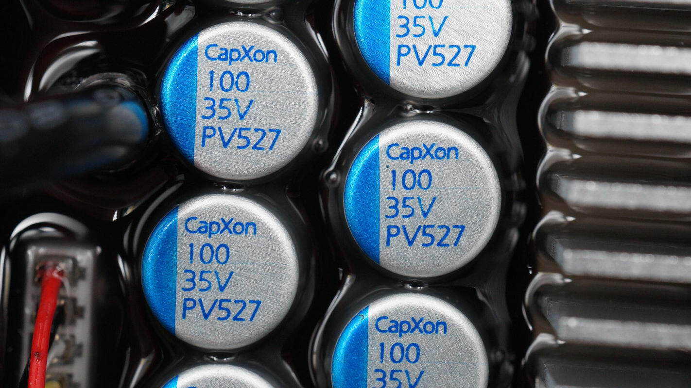
The filter capacitors on the opposite side are rated at 100 μF, 35 V.
The cement resistor is rated at 10W, 75Ω.
This filter capacitor is rated at 100 μF, 16 V.
The transformer core is insulated with tape winding.
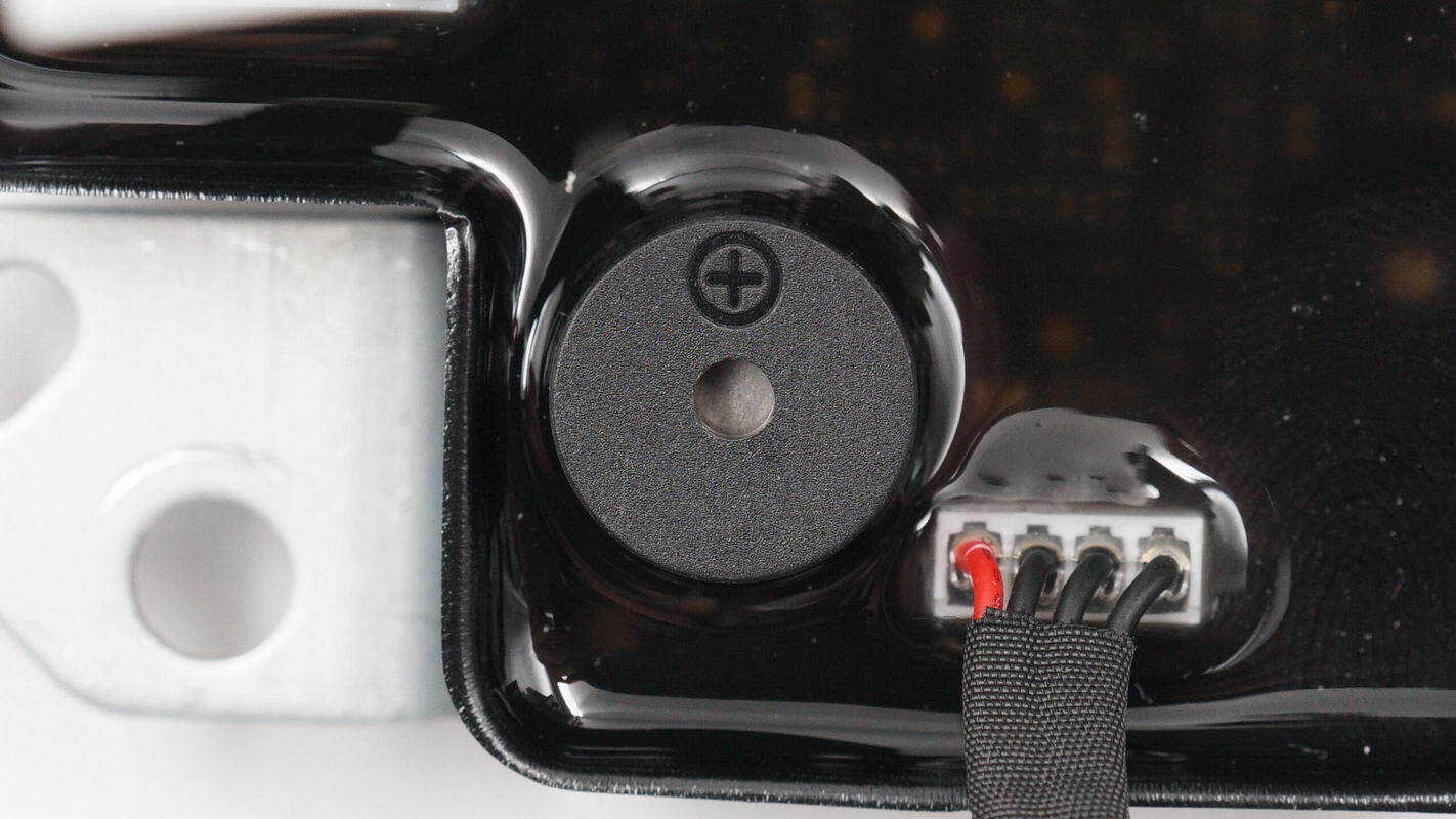
The buzzer is used for operational alerts.
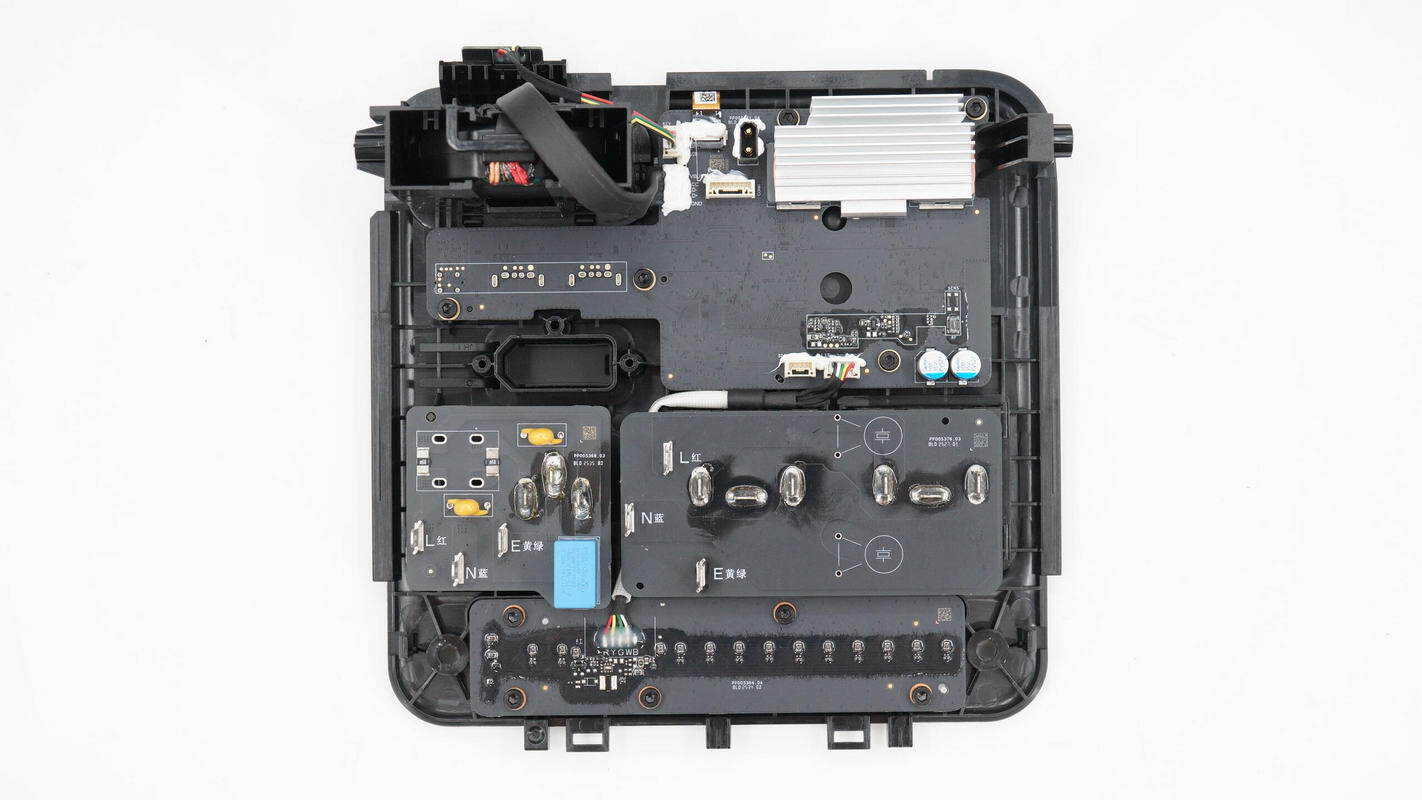
Inside the panel, there is a display panel. The AC input and inverter output sockets are connected via PCB soldering, and the bottom features a PCB for the LED lighting.
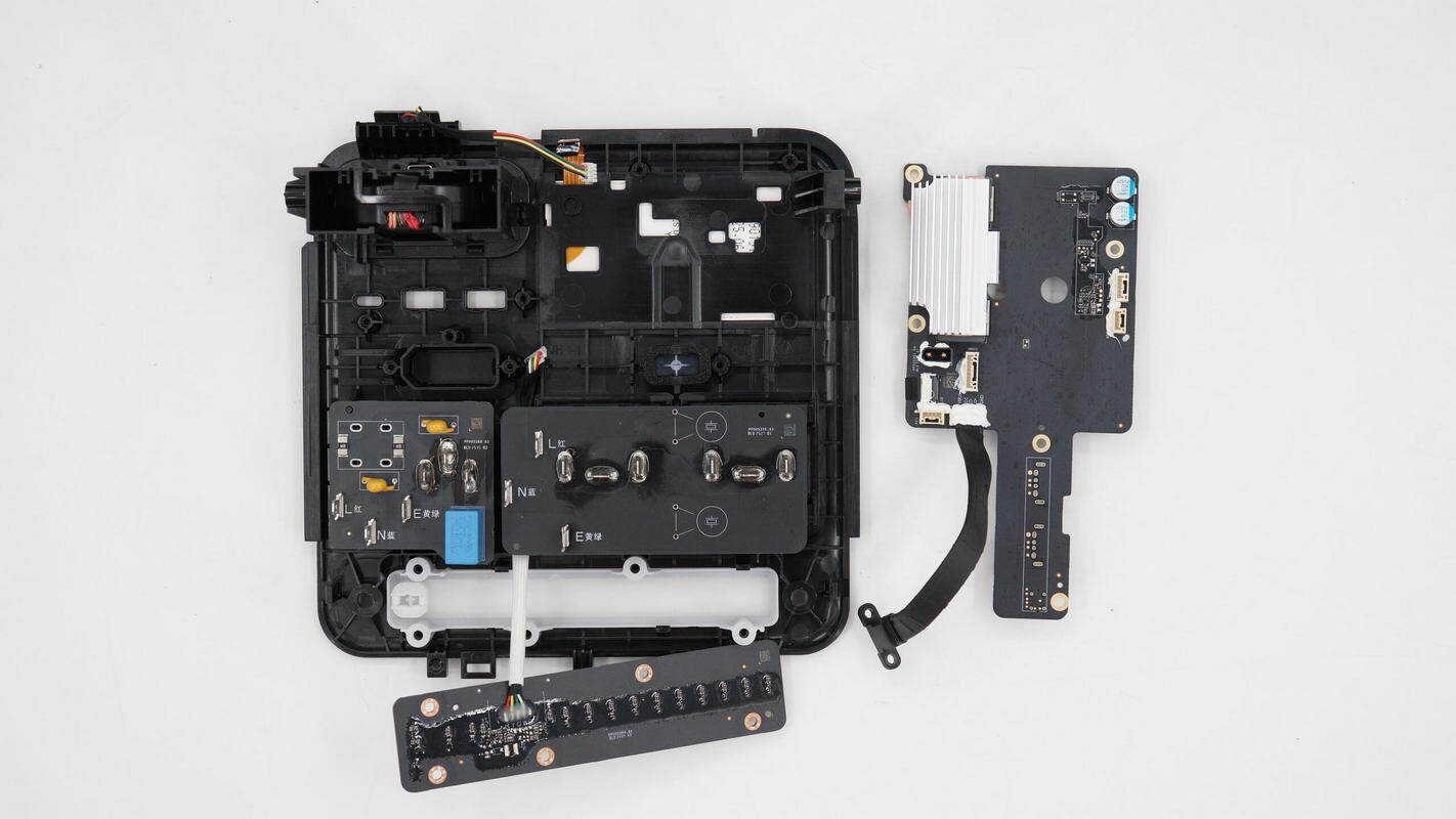
Unscrew the screws and remove the display panel and the LED lighting PCB.
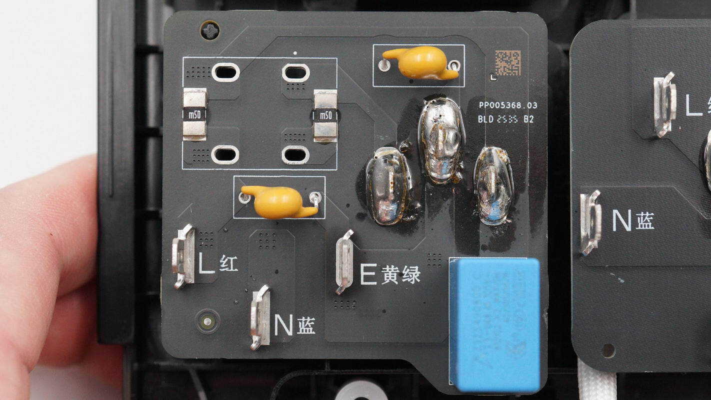
The AC input PCB is soldered with a safety X2 capacitor, yellow Y capacitors, and current-sensing resistors.

The safety X2 capacitor is from TDK, with a rating of 0.68 μF.
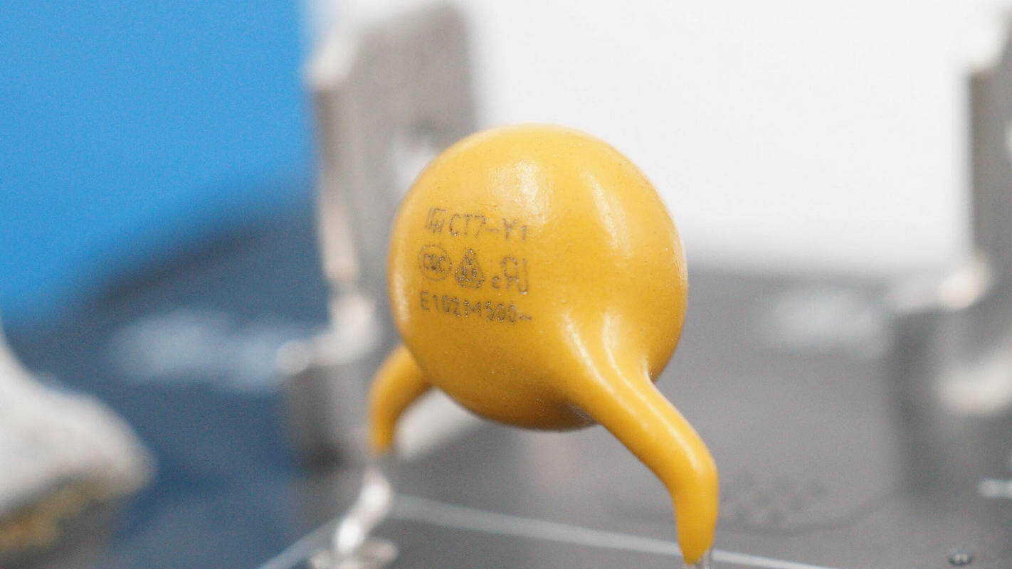
The yellow Y capacitors are from FNR, with the part number E102M.
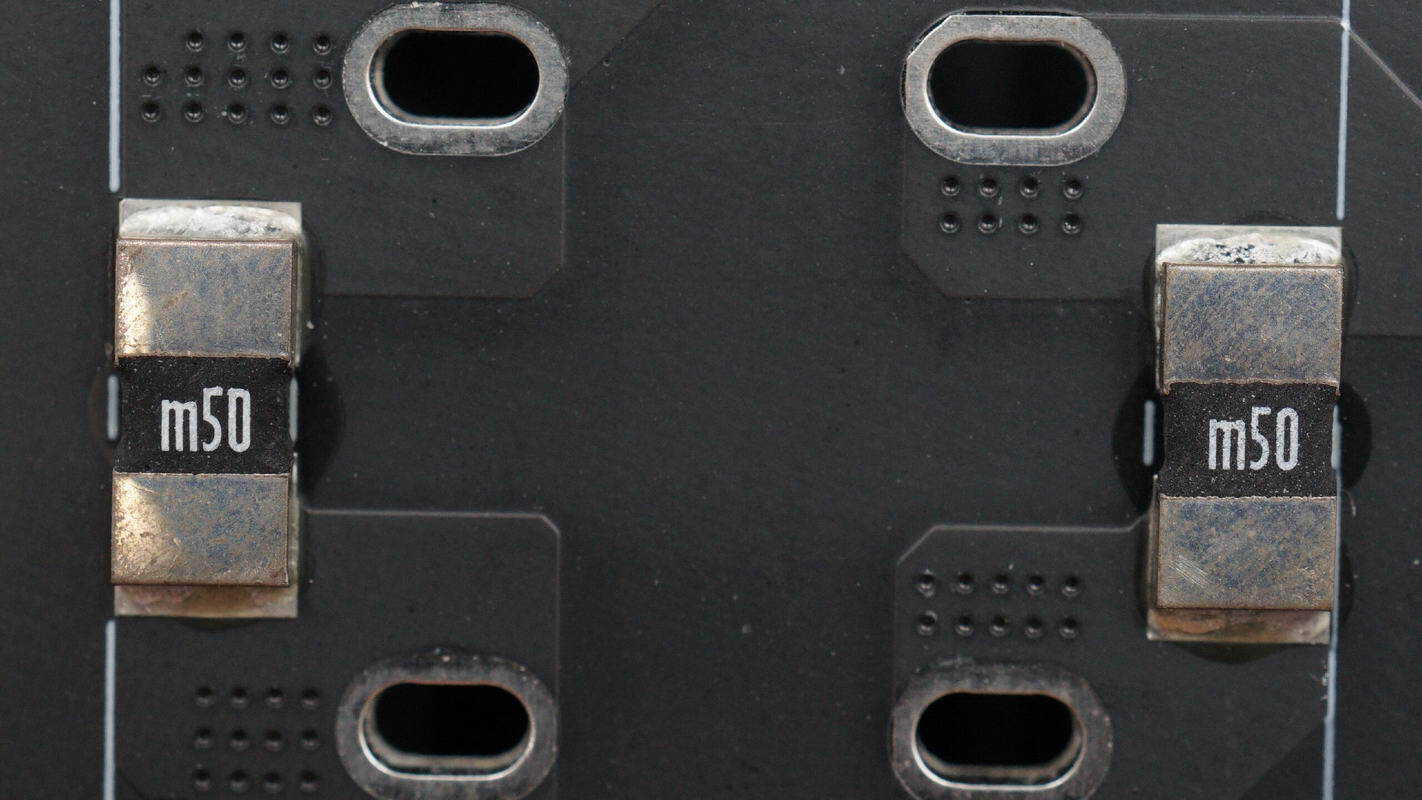
Close-up of the two 0.5 mΩ current sensing resistors.
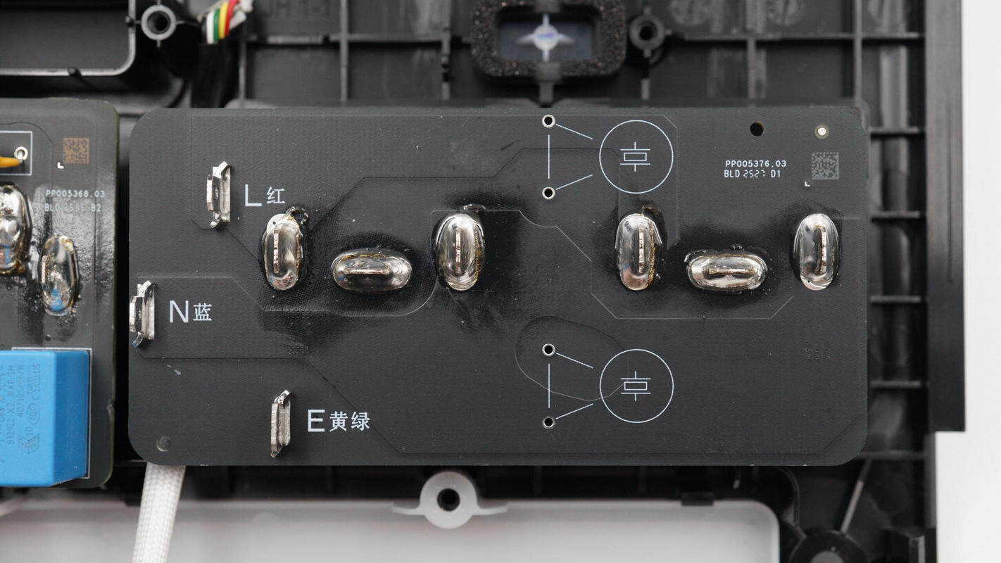
The output sockets are connected via PCB soldering.
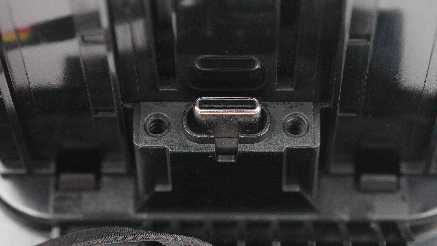
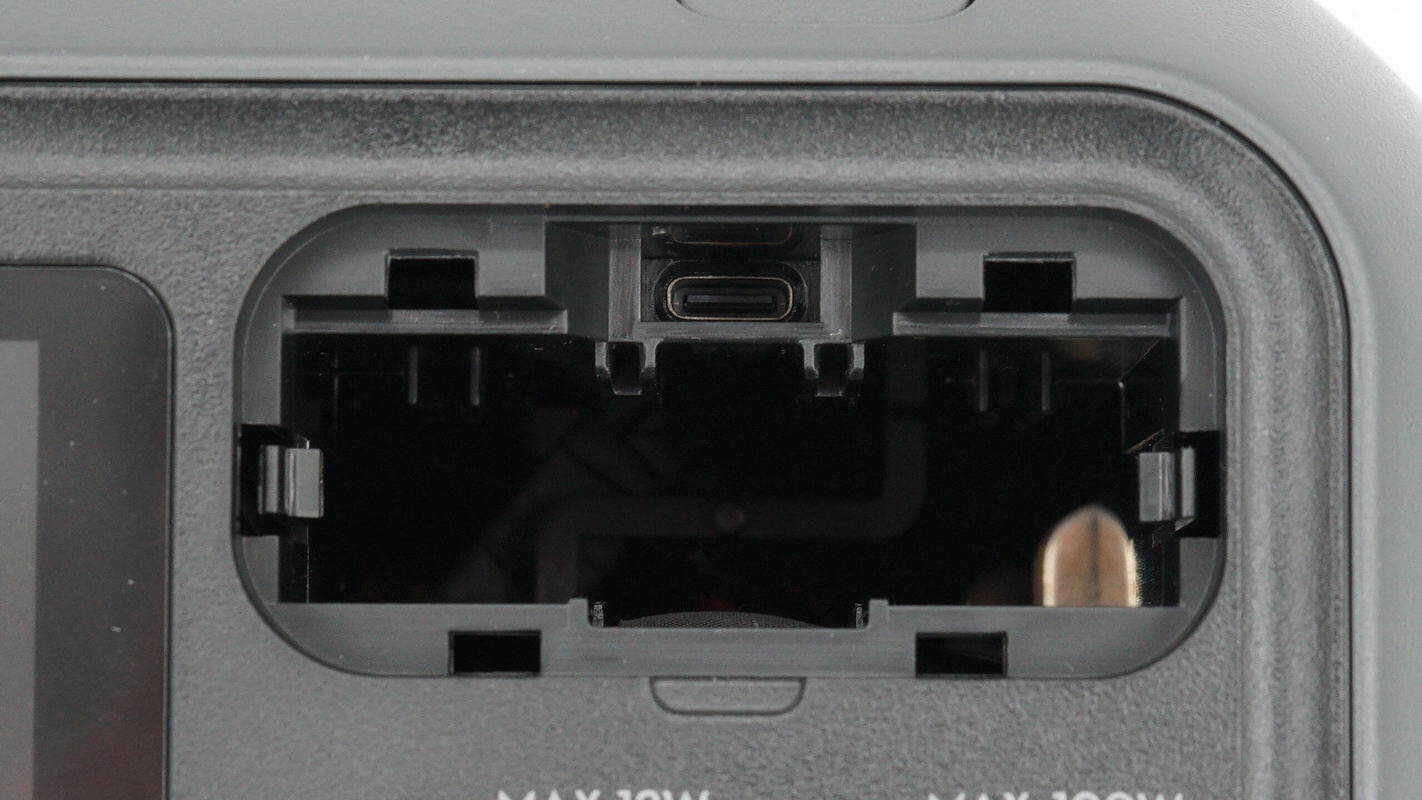
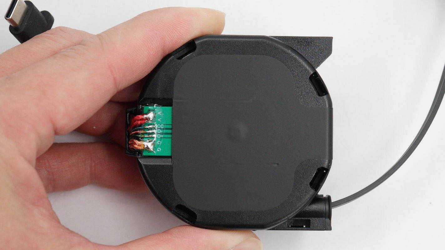
Close-up of the USB-C socket connecting the retractable cable module.

The power switch and LED indicator are soldered onto a separate small PCB.
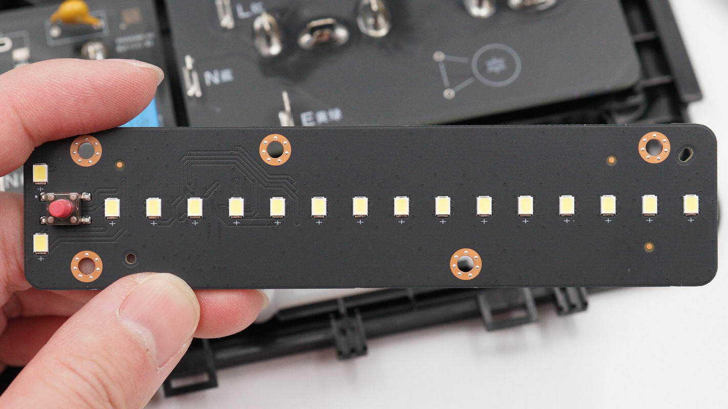
The lighting PCB is soldered with the switch button and the LED lighting.
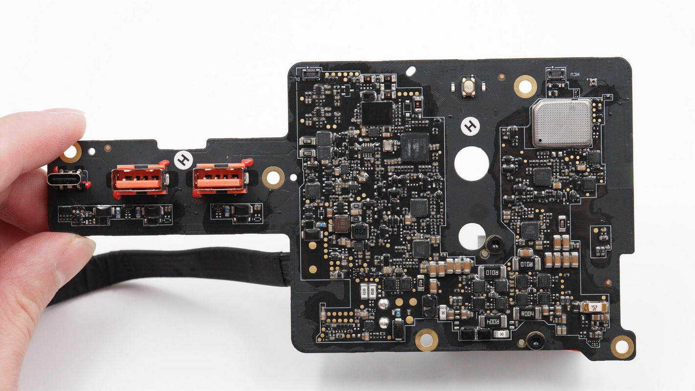
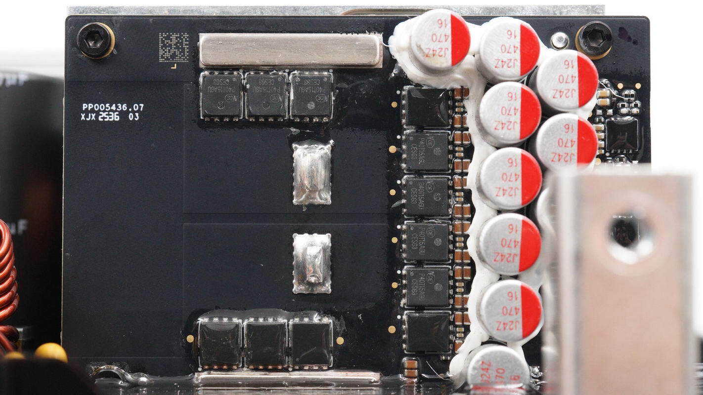
The left side of the side panel features USB-C and USB-A ports. On the other side, there are an MCU, synchronous buck-boost controllers, protocol chips, and MOSFETs. Inside the shielded enclosure, there is a wireless communication chip.
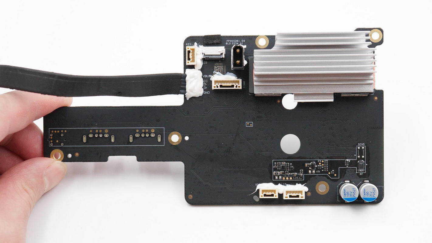
The back side features connection sockets, a heatsink, and filter solid capacitors.

Below the heatsink, there are inductors, which are coated with thermal gel to enhance heat dissipation.

The MCU is from GigaDevice, model GD32F470VGH6. It features a Cortex-M4 core with a clock speed of 240 MHz, an integrated FPU and DSP, 1MB of FLASH memory, and 512KB of SRAM. It also supports a comprehensive set of communication interfaces and comes in a BGA100 package.
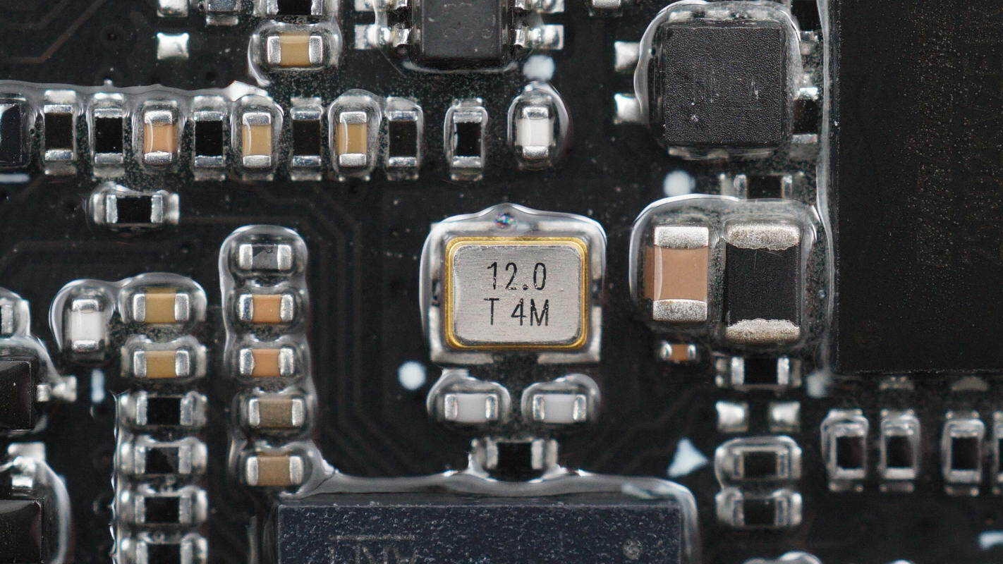
Close-up of the 12.0 MHz crystal oscillator.

The memory is from Winbond, model W25N02KVZEIR. It has a capacity of 256MB, featuring built-in SLC flash memory, and comes in a WSON-8 package.
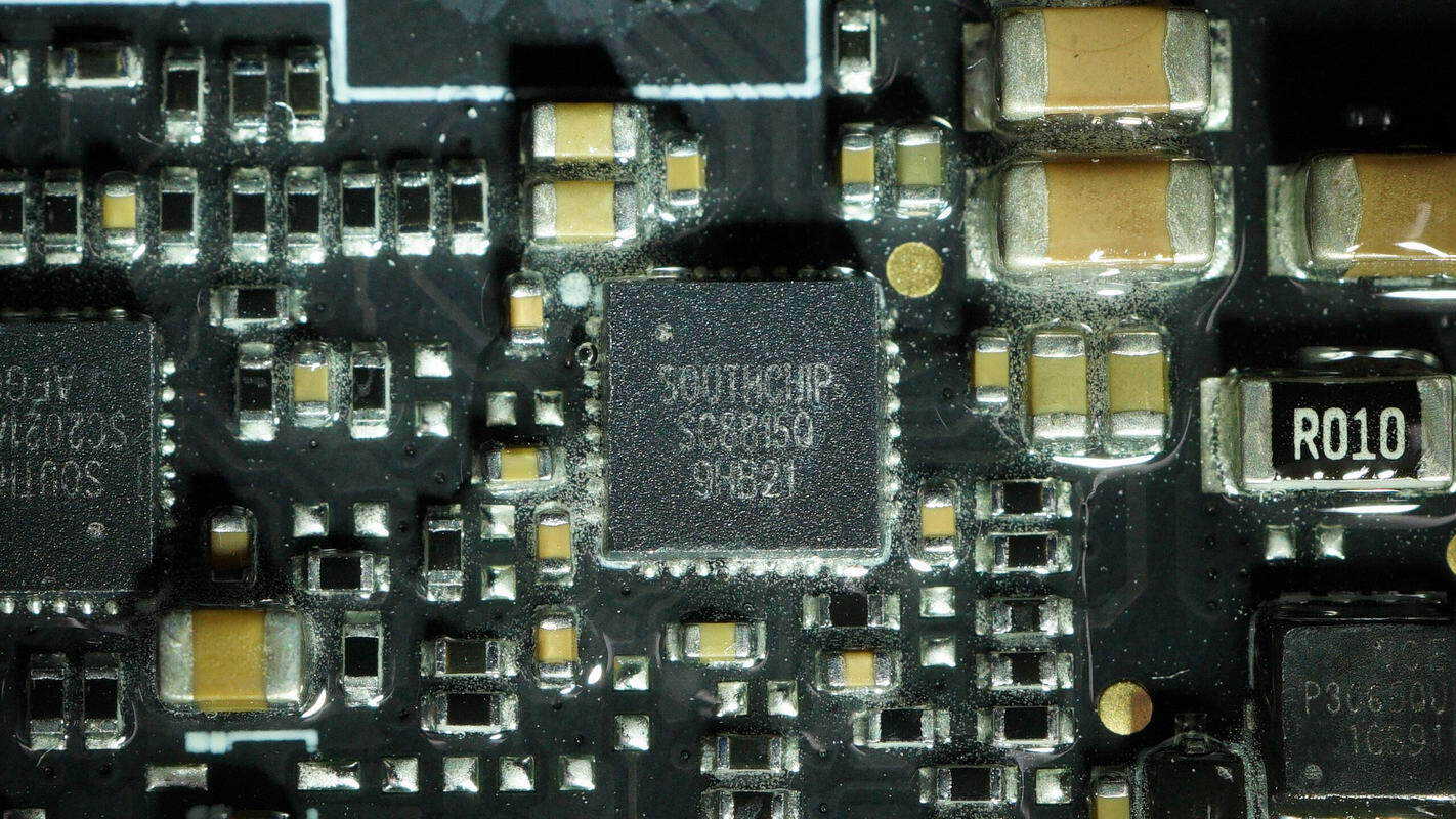
The synchronous buck-boost controller used for the USB-C voltage conversion is from SouthChip, model SC8815Q. It comes in a QFN32 package.
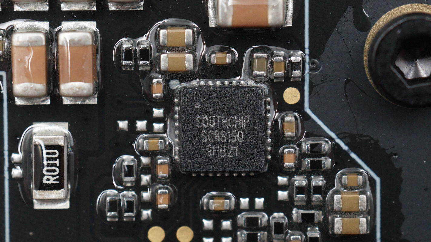
The synchronous buck-boost controller for the other USB-C interface has the same model.

Eight MOSFETs are used for the synchronous buck-boost conversion.
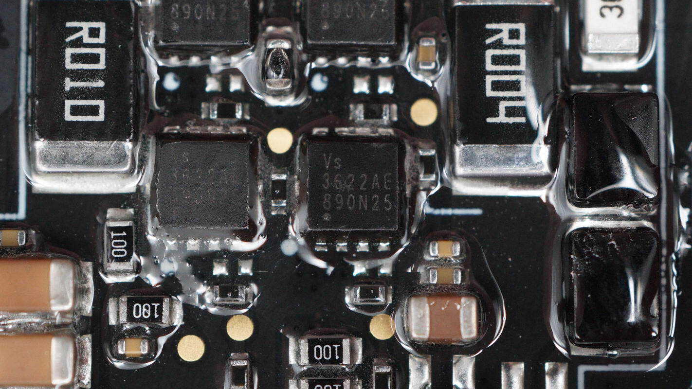
The synchronous buck-boost MOSFETs are from Vergiga, model VS3622AE. They are NMOS transistors, rated at 30 V with an on-resistance of 7.9 mΩ, support 5V logic voltage drive, and come in a PDFN3333 package.
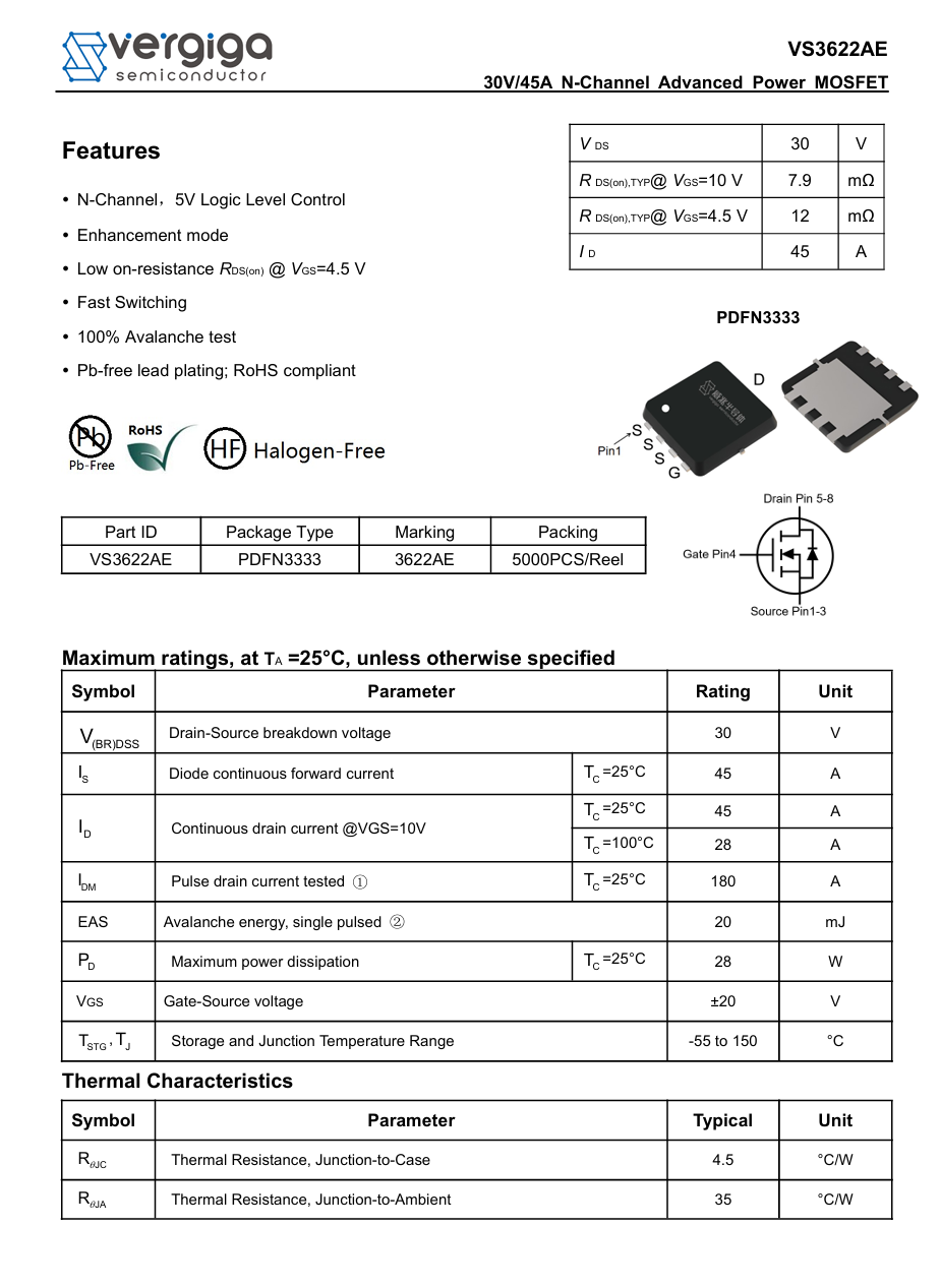
Here is the information about Vergiga VS3622AE.
Beneath the heatsink, there is thermal gel to enhance heat dissipation for the synchronous buck-boost MOSFETs and inductors.
The two 4.7 μH inductors correspond to the two USB-C interfaces.
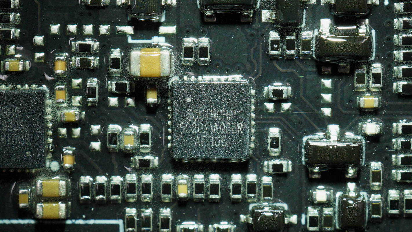
The protocol chip is from SouthChip, model SC2021A. It is a highly integrated Type-C/PD and DPDM fast charging controller that has passed USB PD3.1 compliance testing. It supports proprietary high-voltage fast charging protocols, including one USB-C interface and two DPDM interfaces, catering to 1A+1C dual-port fast charging applications.
The SC2021A integrates a 32-bit high-performance MCU core, 2.5KB of memory, and 32KB of MTP storage. It supports proprietary fast charging protocols. The chip comes in a QFN 4×4-32 package and offers excellent protocol compatibility along with rich control interfaces, making it suitable for car chargers and fast charging applications.
Here is the information about SouthChip SC2021A.
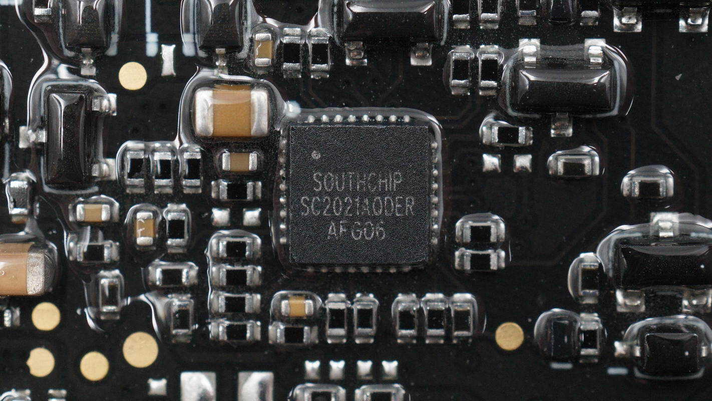
The other protocol chip has the same model.

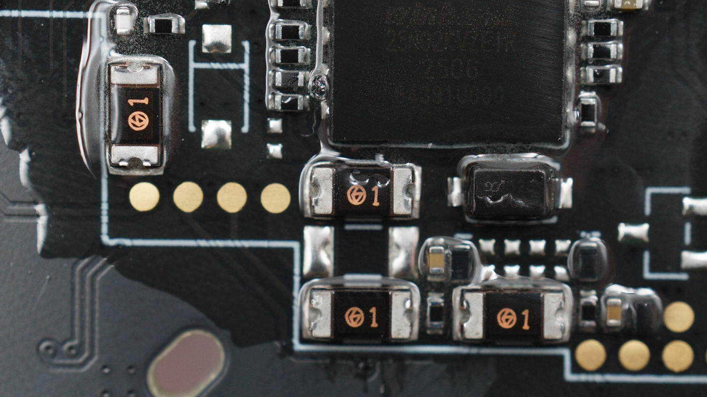
The VBUS MOSFETs are from NCE, model NCEP3065QU. They are NMOS transistors, rated at 30 V with an on-resistance of 1.9 mΩ, and come in a DFN 3.3×3.3 package. These are used for controlling the built-in cable output.
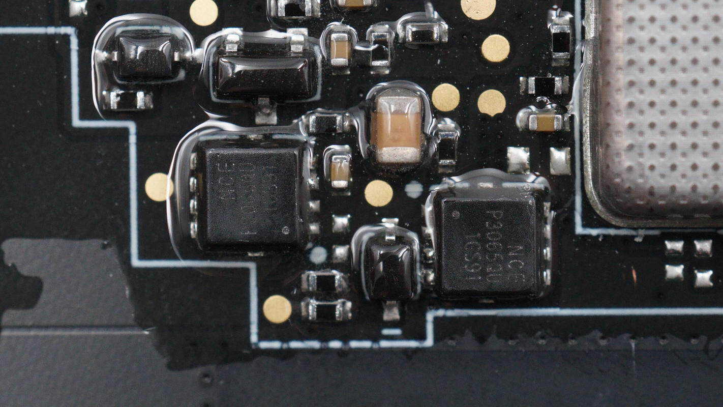
The other two MOSFETs of the same model are used for USB-C output control.
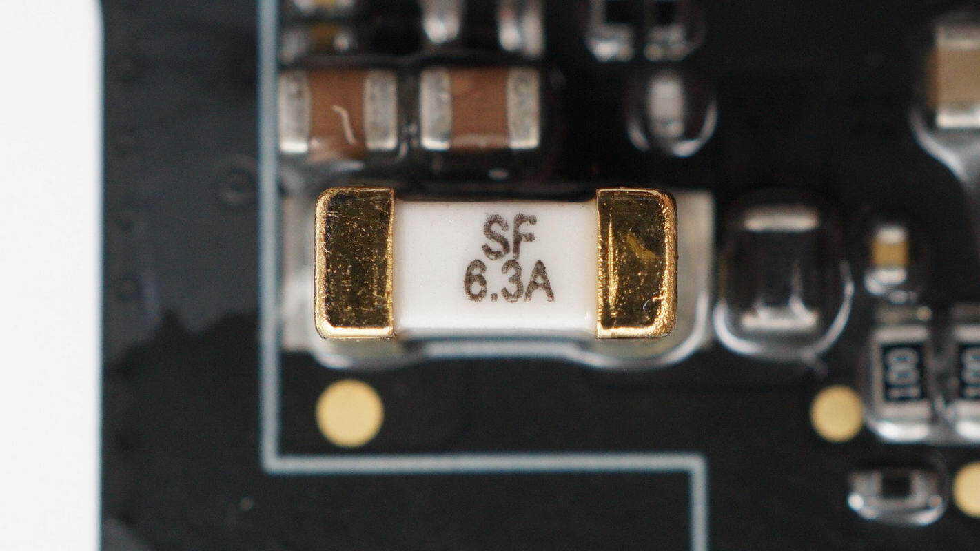
The SMD fuse is rated at 6.3 A.

The synchronous buck regulator chip is from Silergy, marked with BAF, model SY8366H. It is a synchronous buck converter with integrated MOSFETs, supporting an input voltage range of 4–28V. The chip operates at a switching frequency of 800kHz, supports a continuous output current of 6A, and a peak output current of 12A. It features programmable peak current limiting, output discharge functionality, and over-temperature protection. The chip comes in a QFN 3×3-12 package.
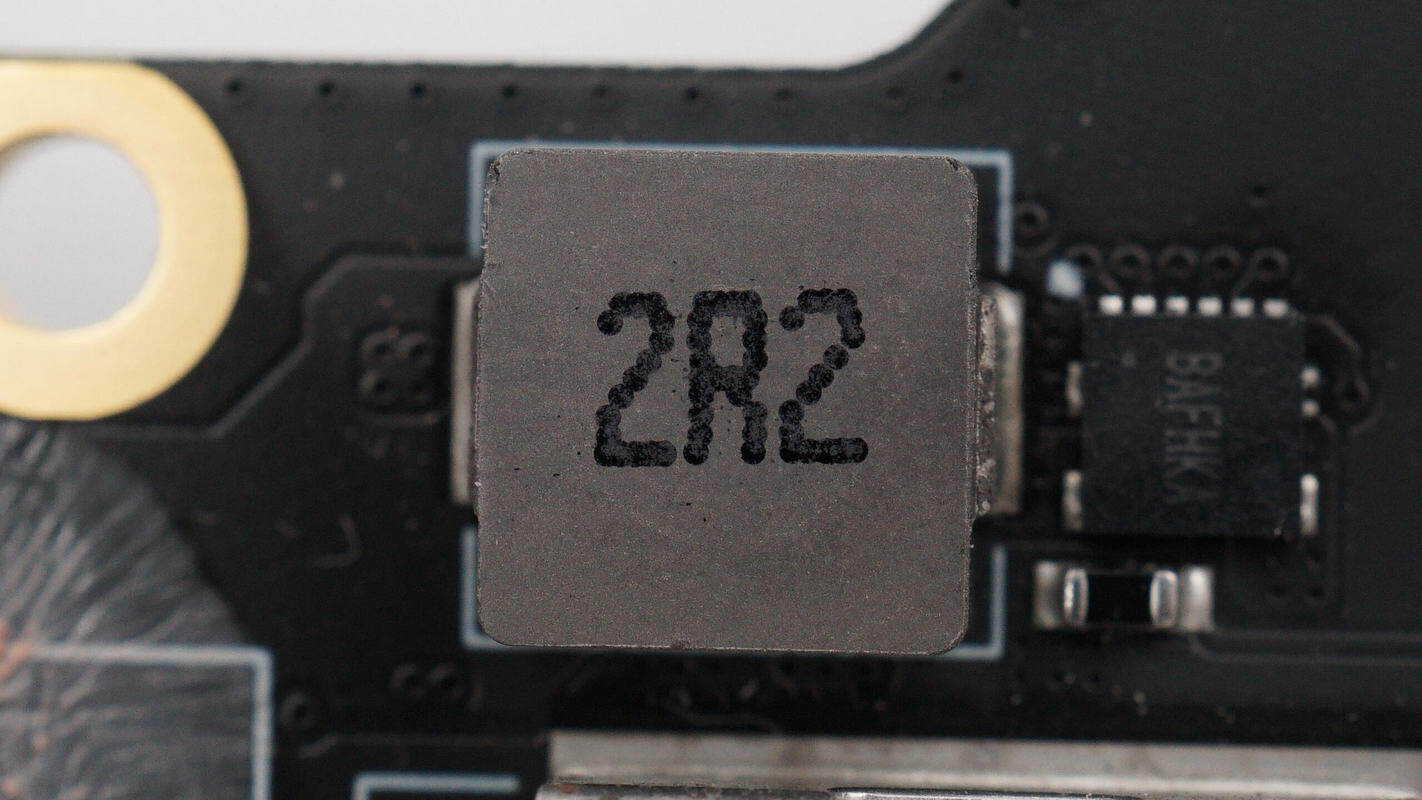
Close-up of the 2.2 μH inductor used in combination with the synchronous buck converter.

The three VBUS MOSFETs are marked with Q40P03 and come in a DFN3333 package. Two 10 mΩ resistors are used for detecting the USB-A interface output current.
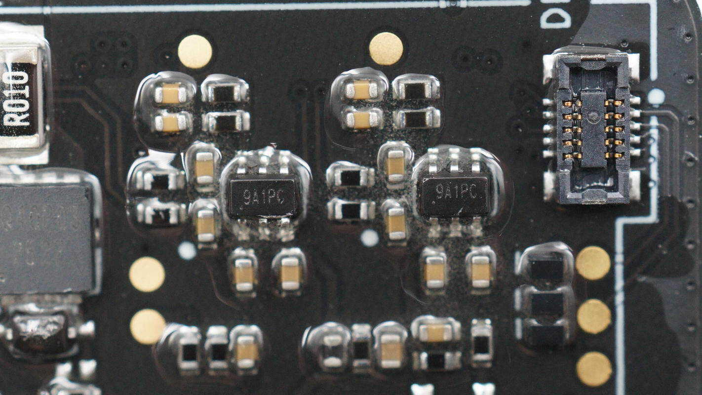
The current sensing chips are from 3PEAK, marked with 9A1, model TP181A1. They are zero-drift, bidirectional current sensing amplifiers, and come in SC70 packages.

Both the USB-C and USB-A connectors are fixed in place by through-hole soldering.

The synchronous buck chip is from ETA, marked with "Ld," model ETA8210D. It is a synchronous buck converter with an input voltage range of 4–18V, utilizing adaptive COT (constant on-time) control. The chip supports a 2A output current and features ultra-fast load transient response. It comes in a SOT23-6 package.

Here is the information about ETA ETA8210D.

Close-up of the 4.7 μH buck inductor.

The overcurrent protection chip is from ETA, marked with "HM," model ETA6027. It is a programmable current protection load switch that supports a 6V input voltage. The chip features 6.1V overvoltage protection, current limiting from 75mA to 2.2A, fast overcurrent protection, reverse current blocking, over-temperature shutdown, and undervoltage protection. It comes in a DFN 2×2-6 package.

Here is the information about ETA ETA6027.

The screen backlight driver chip is from SGMICRO, model SGM3749. It is a boost LED driver that supports PWM dimming. The chip supports a 20V input voltage, with a switching frequency of 1.25MHz, and comes in a TDFN 2×2-6L package.
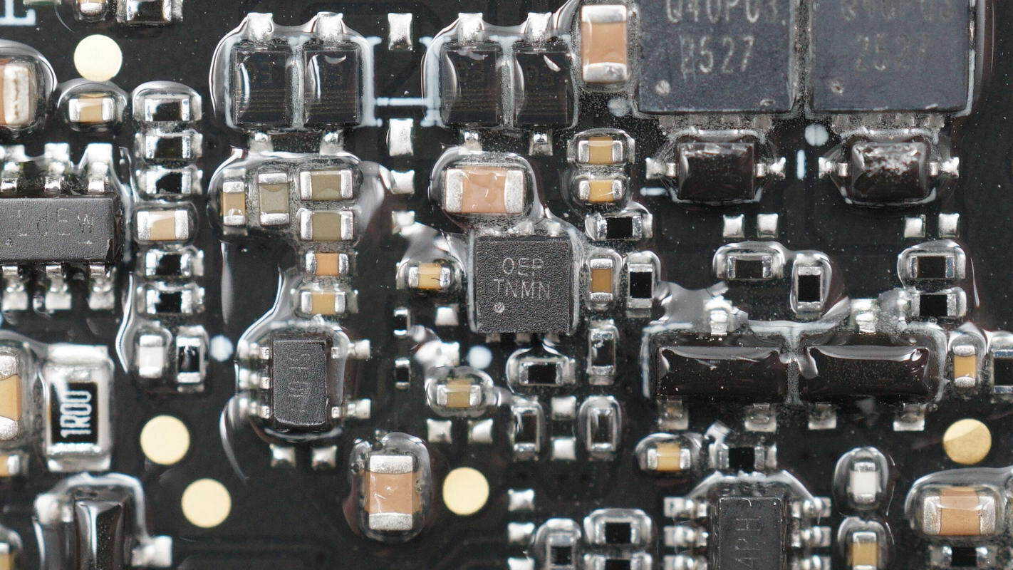
The voltage regulator chip is from SGMICRO, marked with "0EP," model SGM2060-ADJ. It supports a 5.5V input voltage with an adjustable output voltage range from 0.55V to 5V, and a maximum output current of 1A. The chip features current limiting, over-temperature protection, and automatic output discharge. It comes in a TDFN 2×2-6AL package.
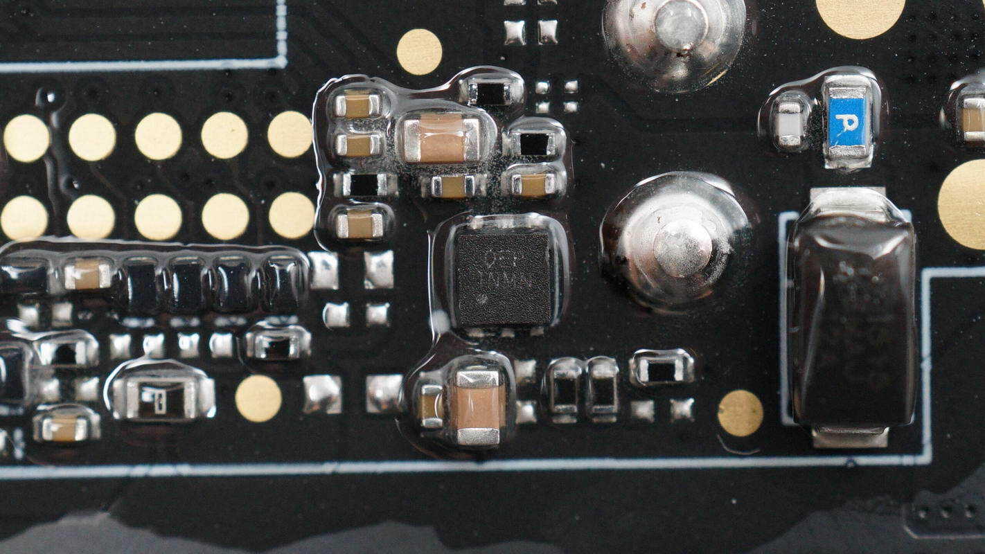
The other voltage regulator chip has the same model.
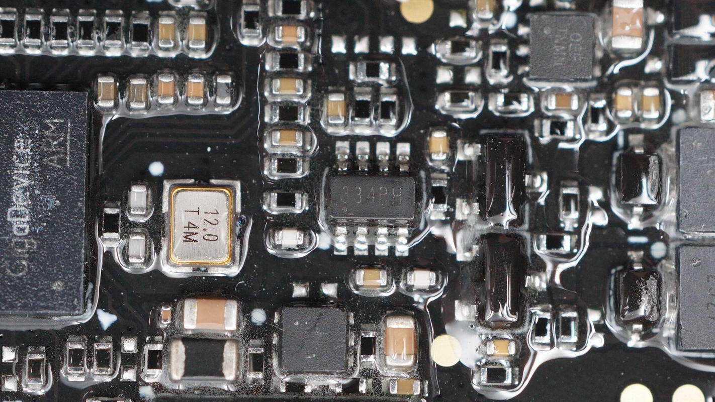
The CAN bus transceiver is from 3PEAK, marked with "334," model TPT1334. It supports a 3.3V supply voltage and a 2.8–5.5V interface voltage. The chip is compatible with the ISO11898 high-speed CAN physical layer standard, supports a data rate of 5Mbps, and includes protections for cross-line and over-voltage conditions. It comes in a SOT23-8 package.
Close-up of the four SMD fuses.
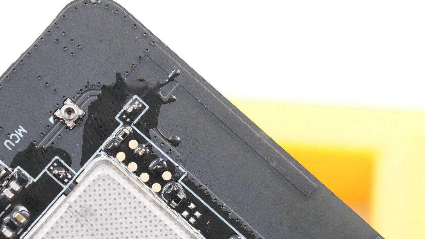
Close-up of the printed wireless antenna used for wireless communication.
The AC output control button is flanked by indicator lights on both sides.
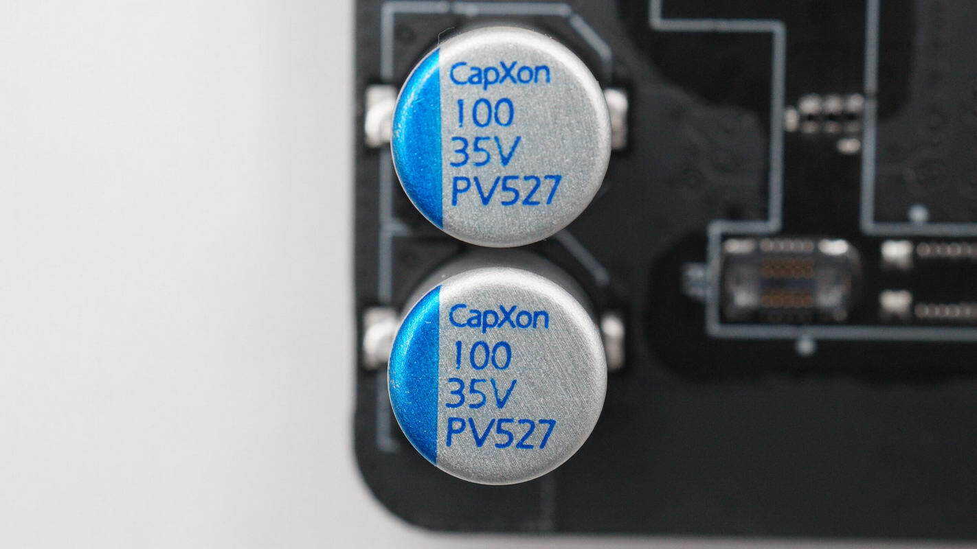
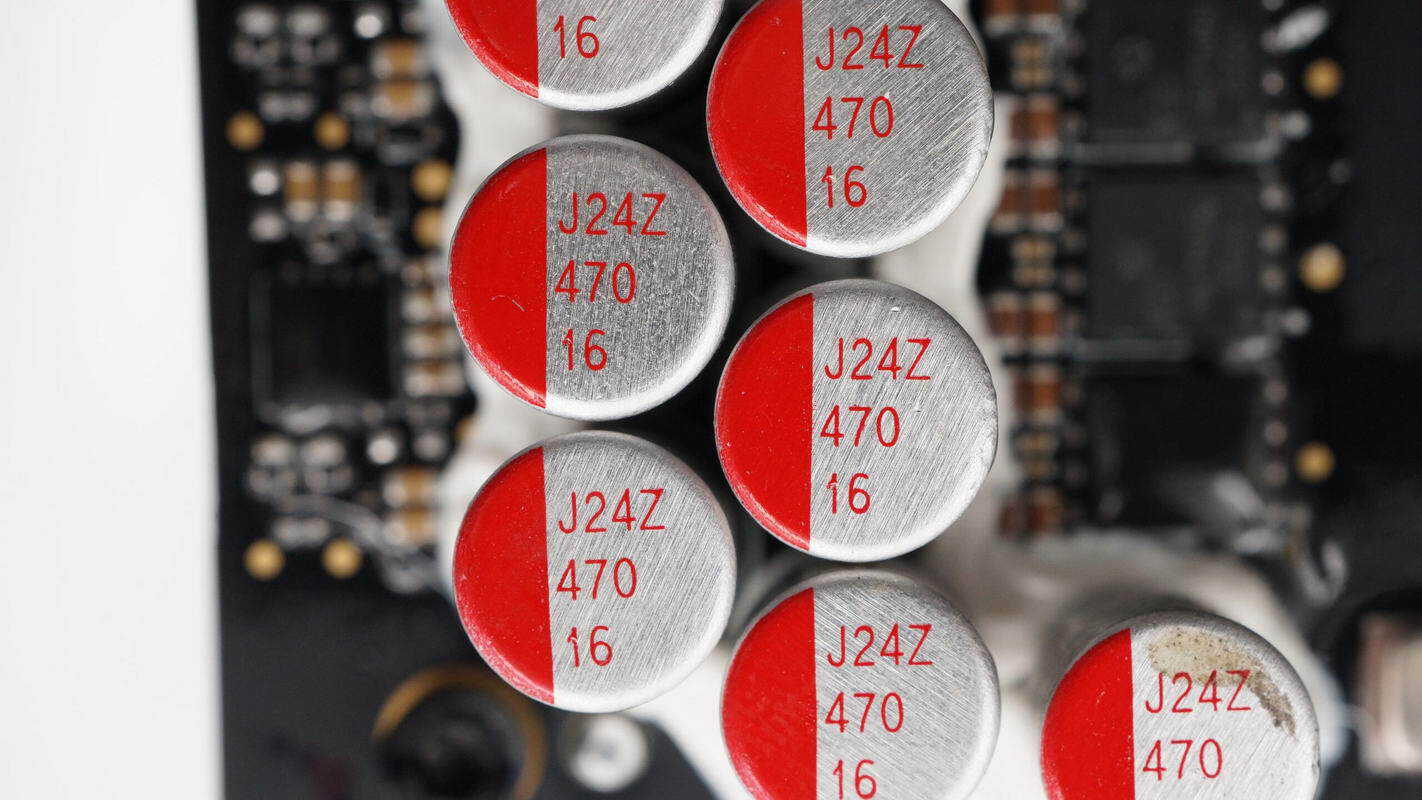
The two filter capacitors are from CapXon, with a specification of 100 μF, 35 V.
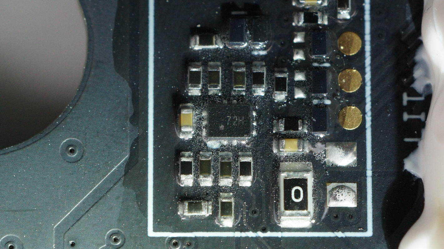
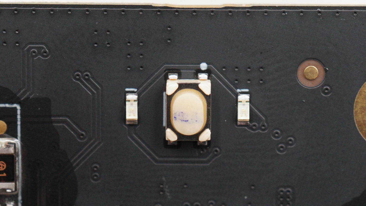
Close-up of the toggle switch marked with "72H."

Close-up of the XT30 connector used for powering the side panel.
Well, those are all components of the DJI Power 1000 Mini Power Station.
Summary of ChargerLAB
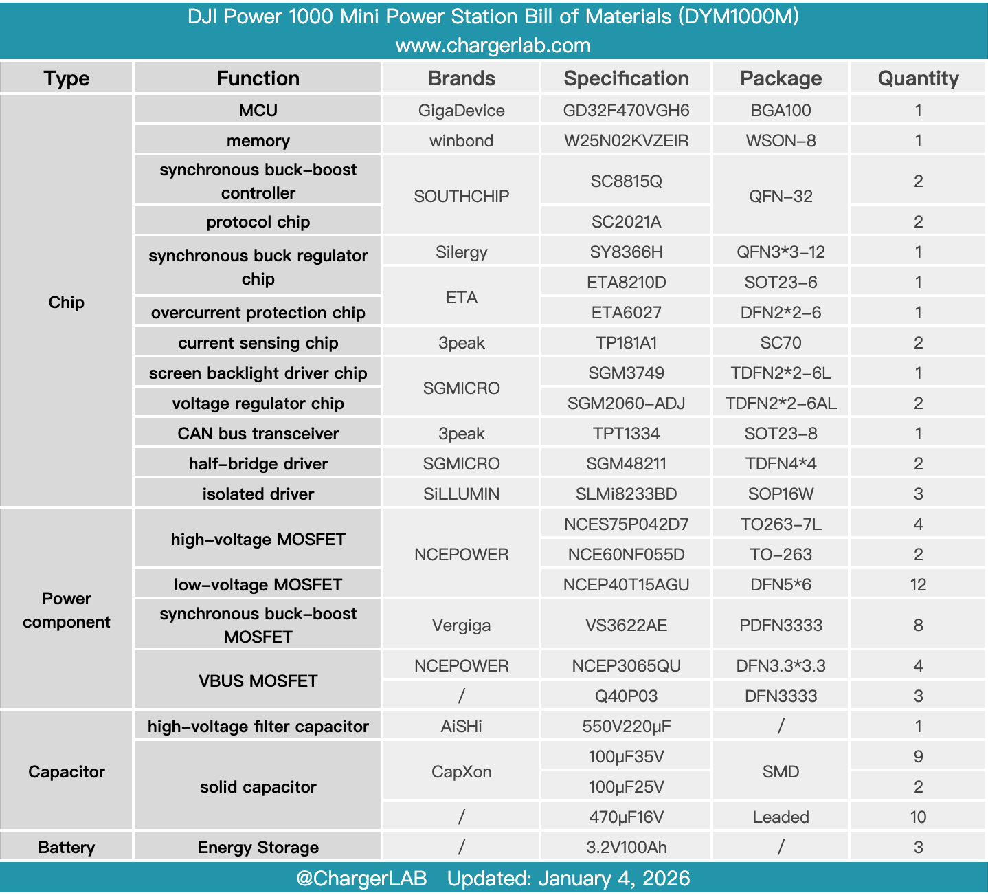
Here is the component list of the DJI Power 1000 Mini Power Station for your convenience.
It features a gray exterior with an integrated handle on the back. The front includes a display screen, USB-C port, USB-A ports, AC input and output sockets, an SDC interface, and a retractable cable. Inside, it is equipped with a 1000Wh lithium iron phosphate battery, supporting a rated output power of 1000W to meet the demands of high-power devices. The USB-C port supports 100W bidirectional fast charging, making it suitable for powering laptops.
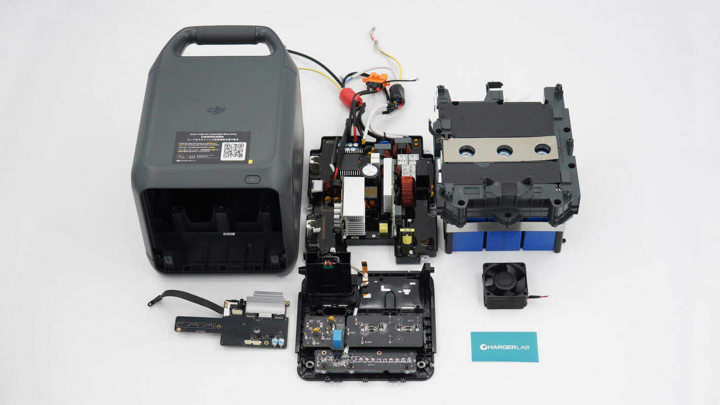
After taking it apart, we found that it adopts a modular design, consisting of a display panel, a bidirectional inverter module, and a battery pack. The battery pack uses square lithium iron phosphate cells, which are insulated with a plastic frame. Metal plates are installed on both sides of the battery for protection, and they are secured with a steel band. Each cell is equipped with a thermistor to monitor temperature. The bidirectional inverter module is encapsulated with a hard resin to provide dust and moisture protection.
The bidirectional inverter module uses NCE NCEP40T15AGU low-voltage MOSFETs, paired with NCES75P042D7 silicon carbide MOSFETs and NCE60NF055D high-voltage MOSFETs. The side panel is powered by the GigaDevice GD32F470VGH6 MCU, while the USB-C interface utilizes SouthChip SC8815Q synchronous buck-boost controllers along with SC2021A protocol chips. Vergiga VS3622AE MOSFETs are used for the buck-boost conversion, and the NCE NCEP3065QU MOSFETs control the VBUS.
The USB-A port buck conversion uses the Silergy SY8366H synchronous buck chip, with the 3PEAK TP181A1 used for output current detection. The ETA ETA8210D is used for buck conversion, paired with SGMICRO SGM2060-ADJ voltage regulator chips to power the MCU. The entire PCBA module is coated with a conformal coating for insulation protection. The synchronous buck-boost inductors and MOSFETs, as well as the inverter MOSFETs, are equipped with heatsinks, complemented by fan cooling. The meticulous craftsmanship and solid materials ensure reliable and safe power usage.
Related Articles:
1. Teardown of Honor Choice LCHSE Clip-On Earphone 2 Pro
2. Teardown of Moore Threads MTT S70 Graphics Card
3. Teardown of Pisen 160W 4-USB-C GaN Charger (TP-C81)