Introduction
Recently, ChargerLAB got the new desktop charger A2345 from the ANKER Prime series. It continues the minimalist design language of the previous generation with a simple and stylish appearance. It is also equipped with 4 USB-C and 2 USB-A ports. The USB-C port supports a maximum of 140W, and the total power reaches 250W.
This new product is also equipped with a 2.26-inch TFT color screen, which can not only display the output power of each port in real-time but also supports clock mode and multiple theme style customization, turning it into an exquisite desk decoration in seconds. In addition, it also supports connecting to the APP or customizing the charging priority and power control of multiple devices through the knob, which is very smart. Next, let's take it apart to see its internal components and structure.
Product Appearance
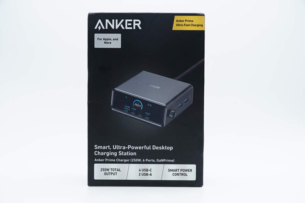
ANKER, appearance, name, and selling points are printed on the front of the box.
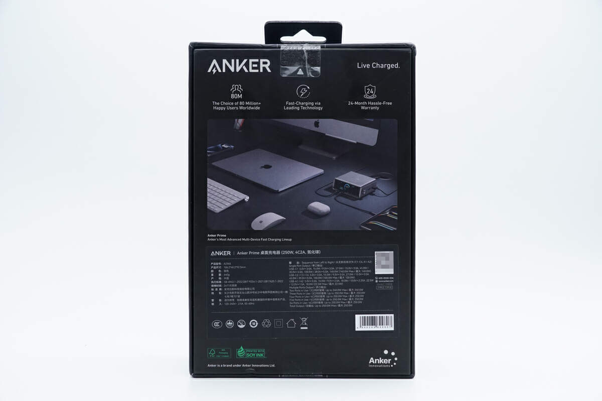
The application scenarios and specs info are printed on the back.
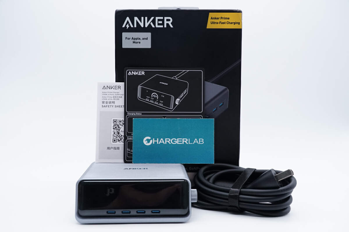
The box contains the charger, power cord, and some documents.
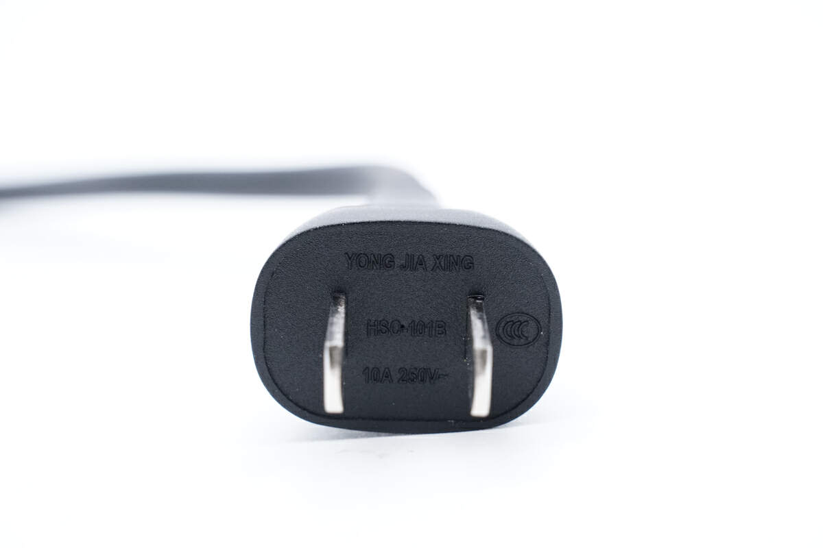
One end of the power cord is a two-pin plug with a specification of 10A 250V~.
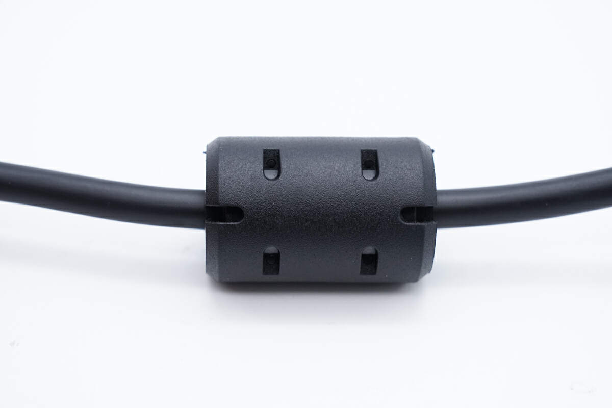
The power cord is equipped with a shielding magnetic ring.
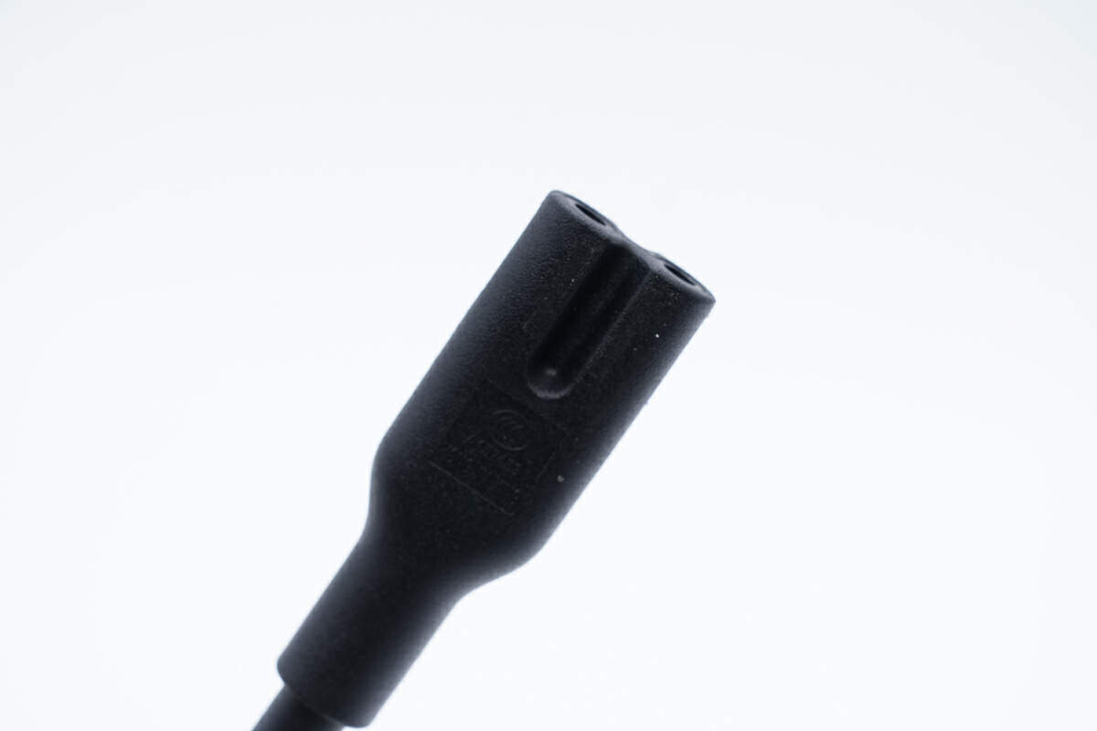
The other end also adopts a 2-prong design.
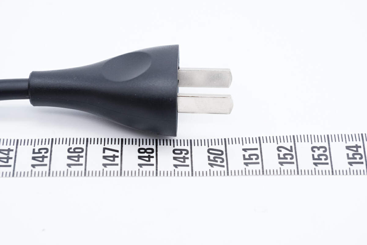
The length of the power cord is about 1.5 m (4' 11.055'').
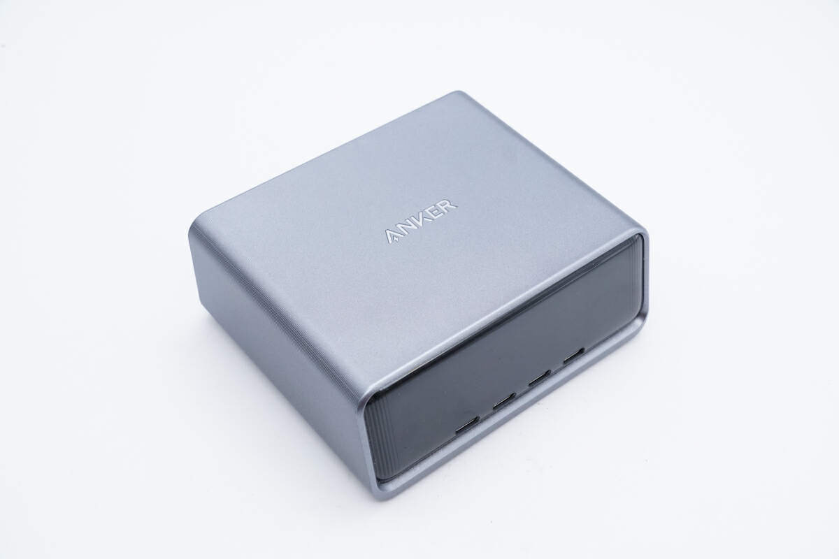
The desktop charger continues the design of the previous generation, using a PC fire-retardant plastic shell. The surface is sprayed with silver-gray metallic paint, and the overall style is simple.
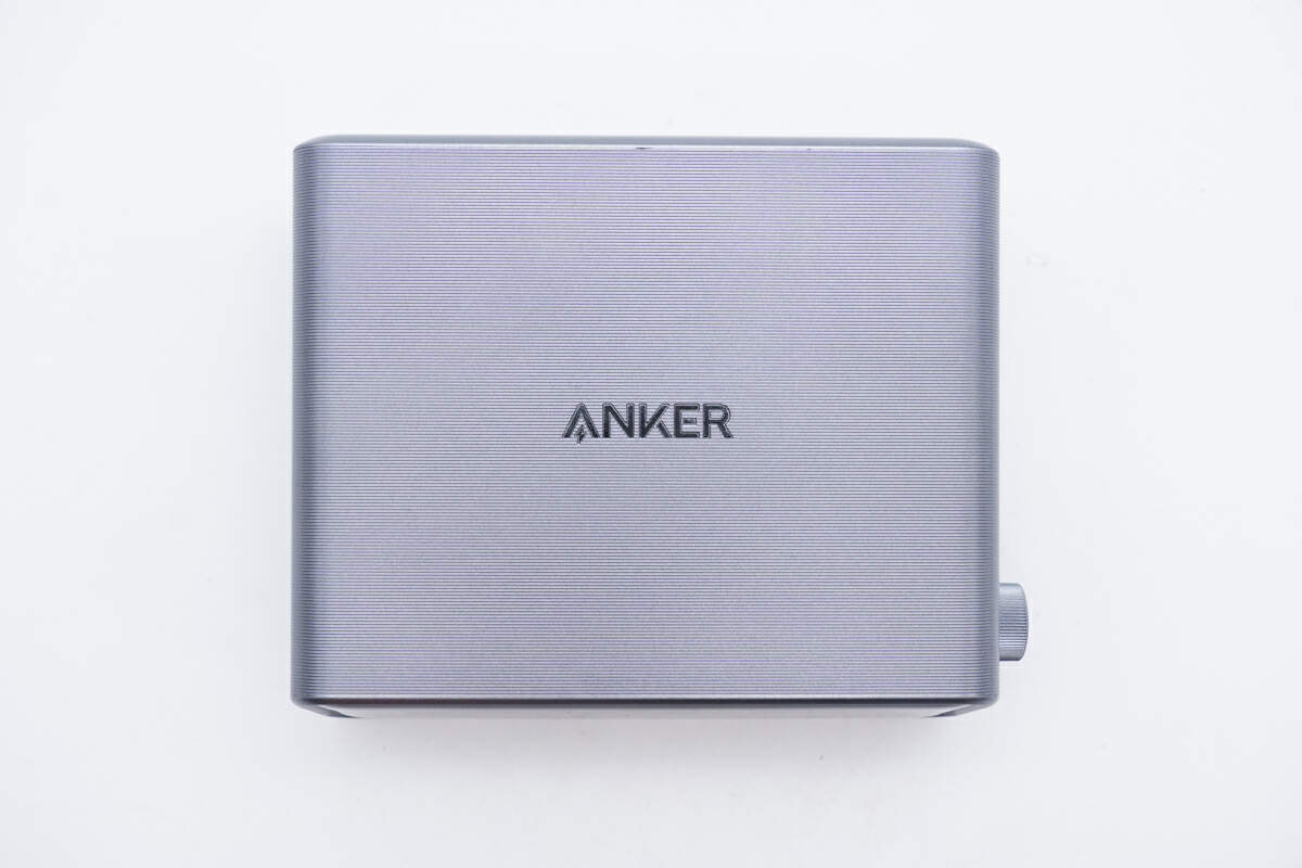
There is an ANKER logo in the center of the top surface.
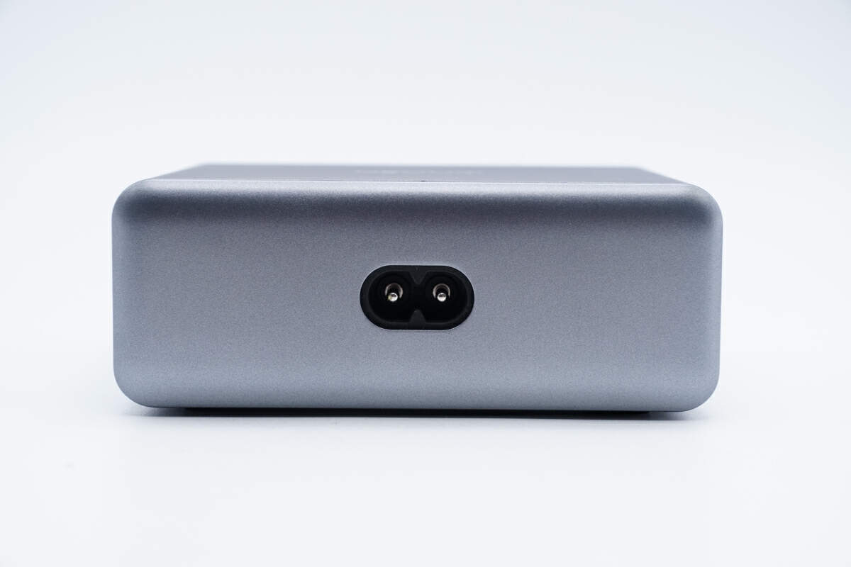
There is an input socket in the middle of the back.
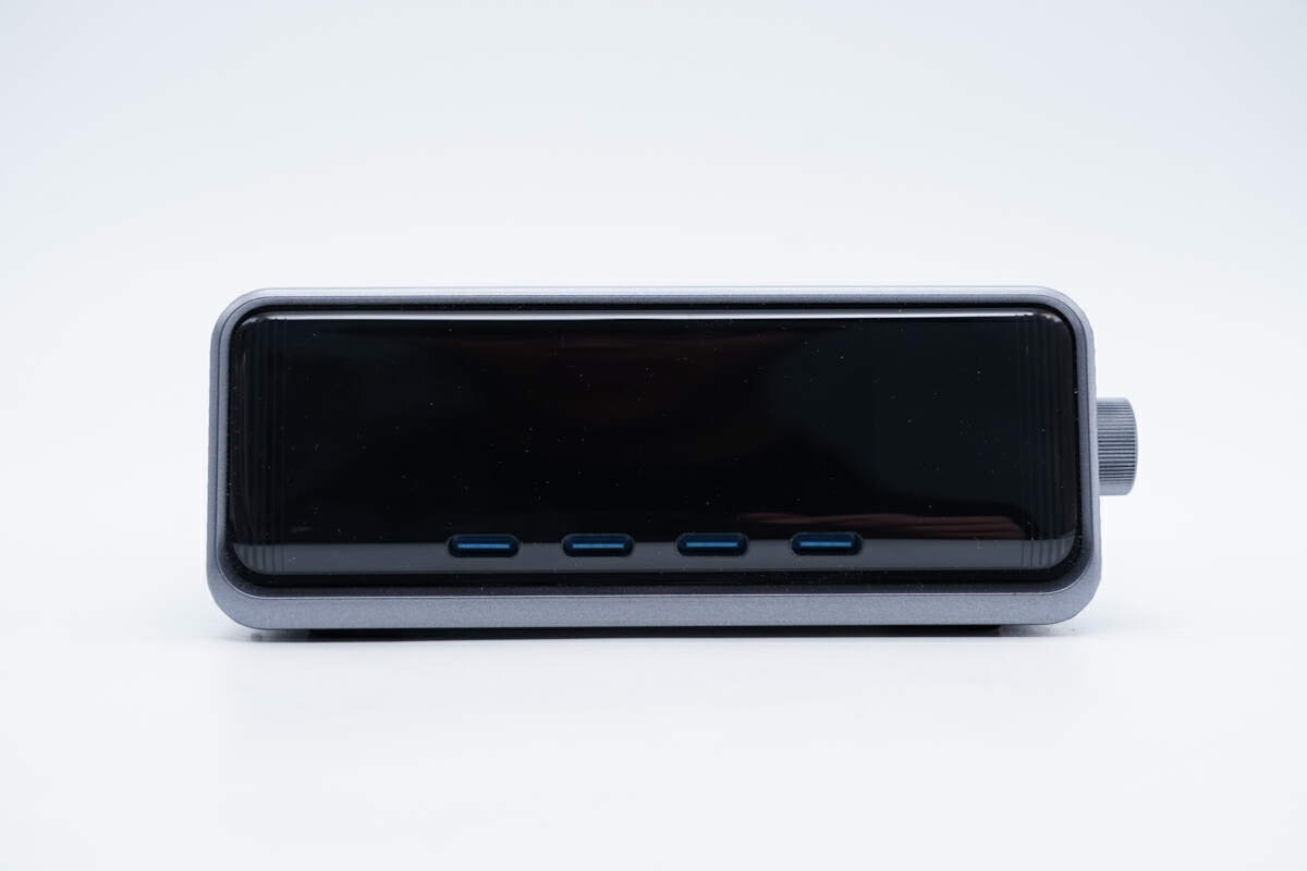
There are 4 USB-C ports and a TFT color screen on the front.
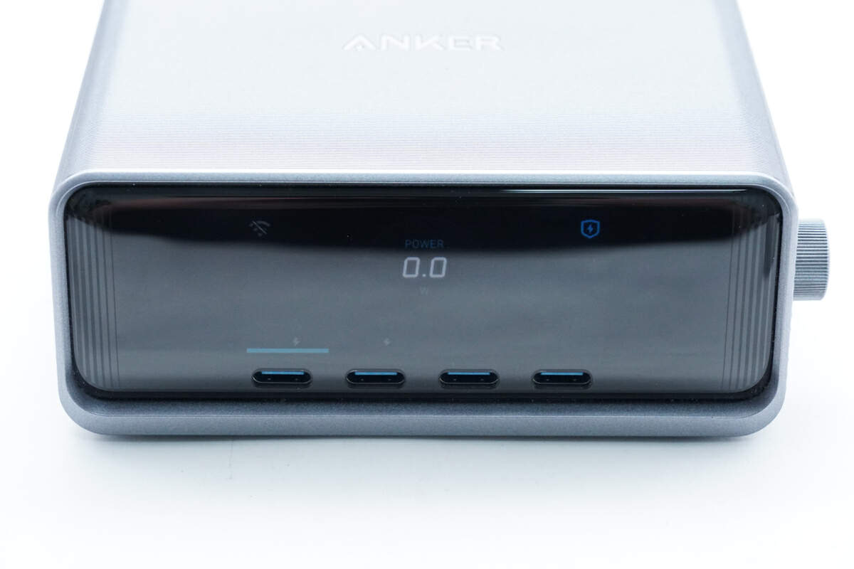
This screen can display the output power of each port, total output power, Bluetooth connection status, security protection status, etc.
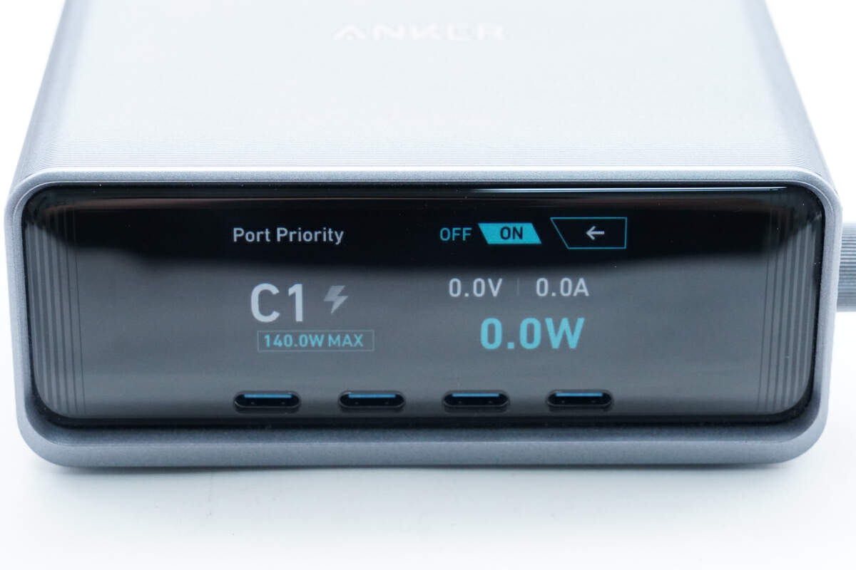
You can also switch to display more detailed output parameters of a certain port, including voltage, current, and power, and customize whether the port is shut down or not. The functions are very comprehensive and flexible.
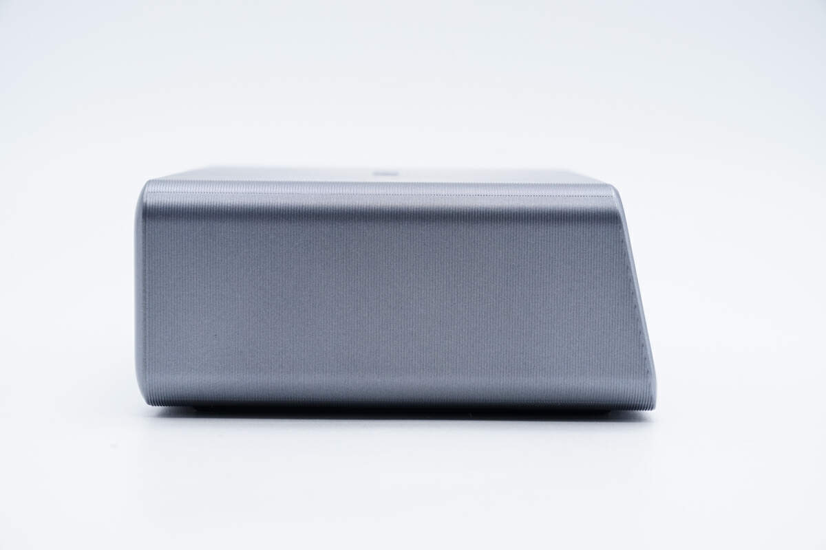
When viewed from the side, the front panel is tilted to allow users to better view the screen.
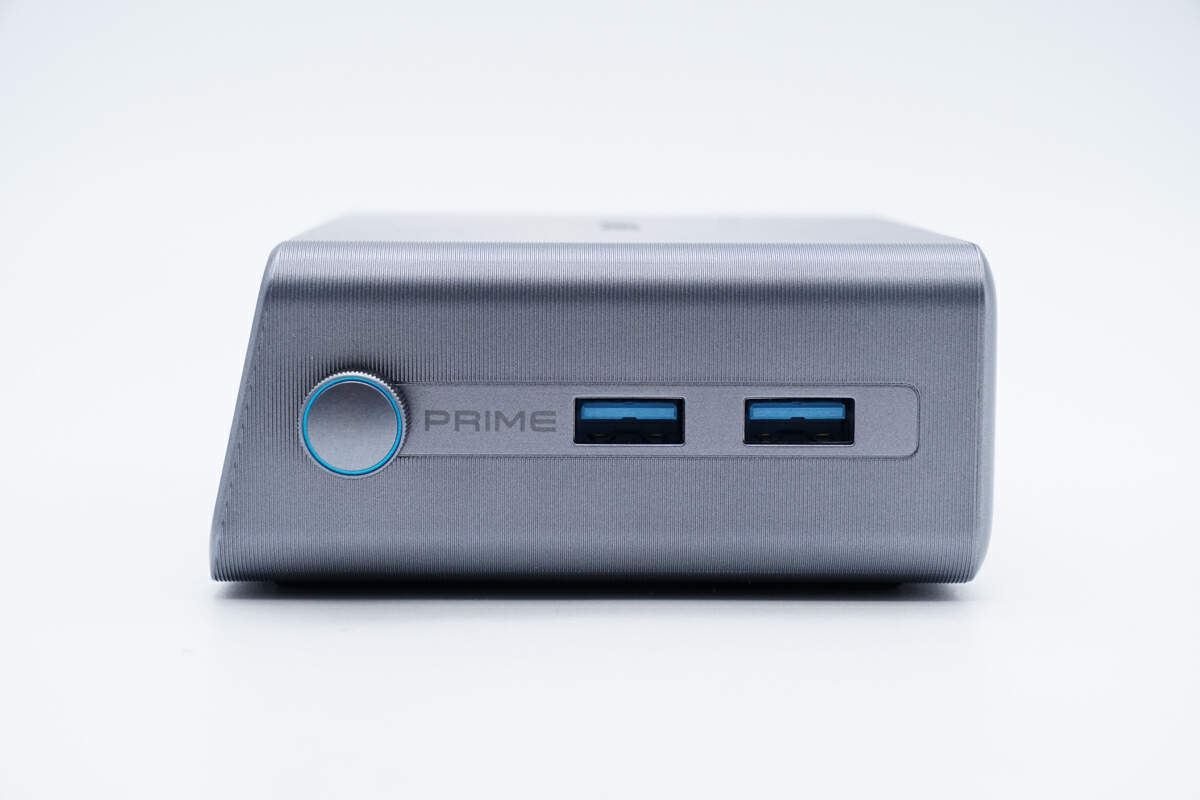
The other side is equipped with an alloy control knob and two USB-A ports.
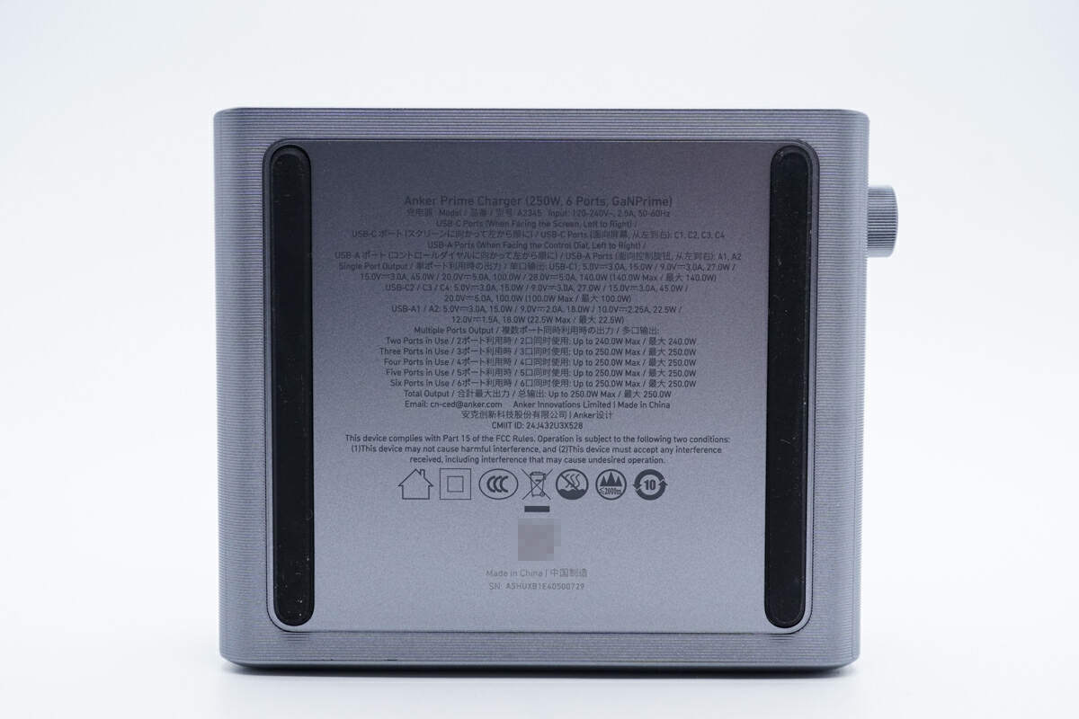
The spec info is printed on the bottom, and there are anti-slip rubber pads on both sides.
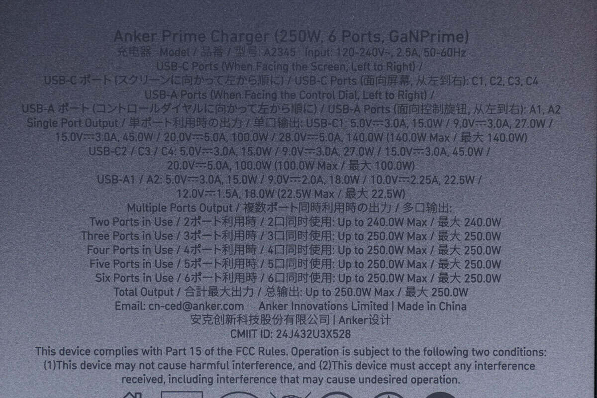
Model is A2345. It can support input of 120-240V~50/60Hz 2.5A. The USB-C1 can support output of 5V3A, 9V3A, 15V3A, 20V5A, and 28V5A. The USB-C2/C3/C4 can support output of 5V3A, 9V3A, 15V3A, and 20V5A. The USB-A1/A2 can support output of 5V3A, 9V2A, 10V2.25A, and 12V1.5A. The total output is 250W.
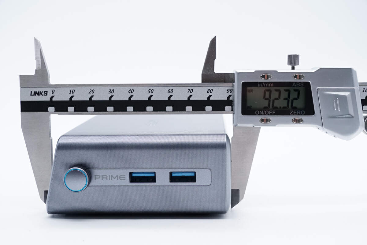
The length is about 92.3 mm (3.63 inches).
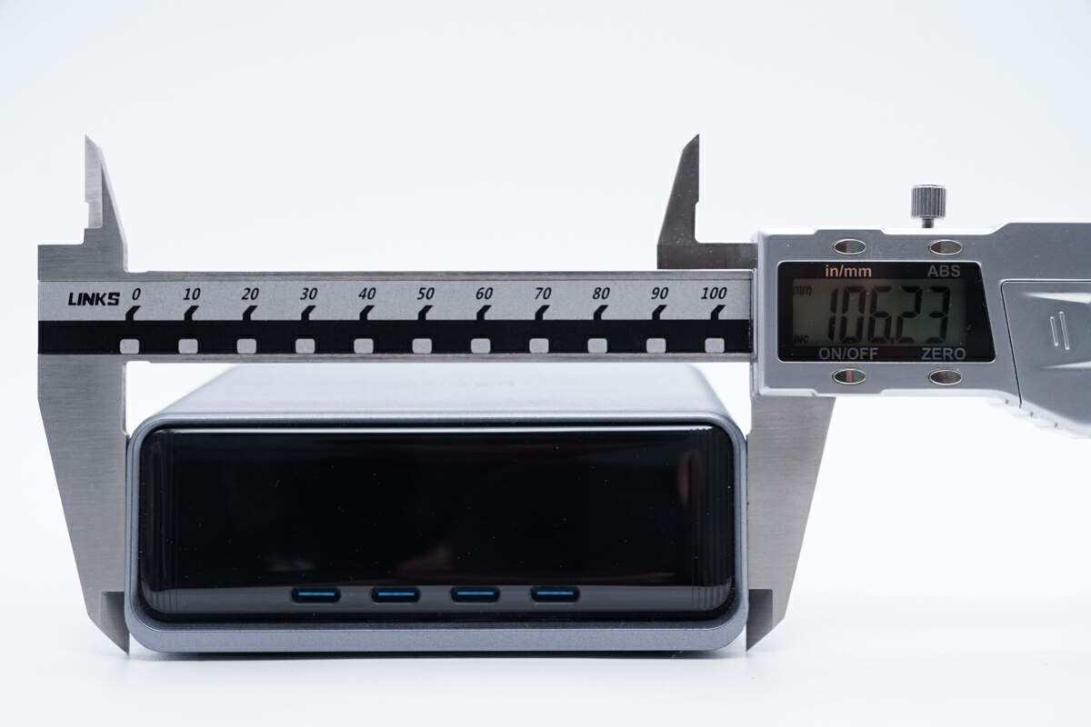
The width is about 106.2 mm (4.18 inches).
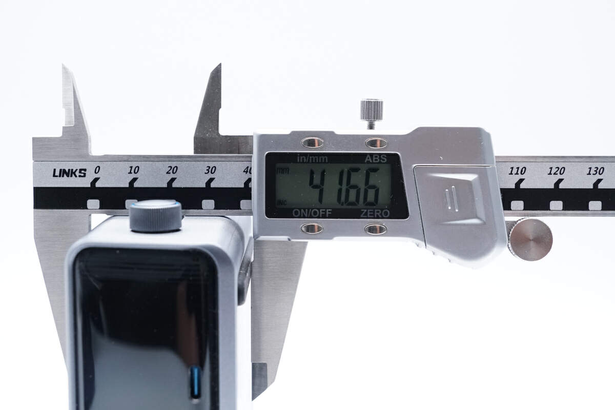
The thickness is about 41.7 mm (1.64 inches).
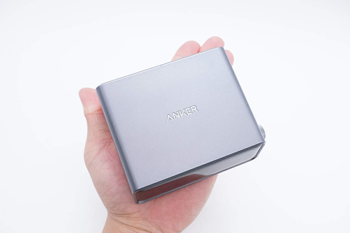
That's how big it is in the hand.
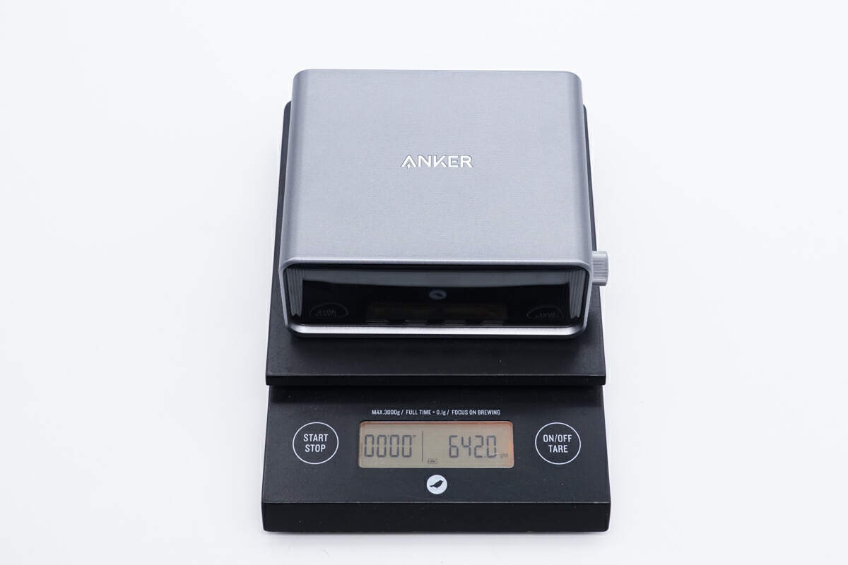
The weight is about 642 g (22.65 oz).
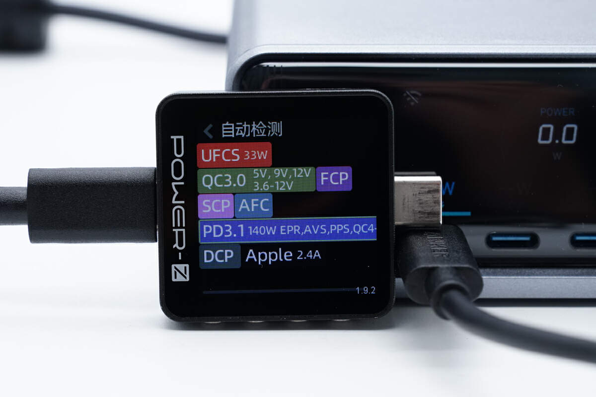
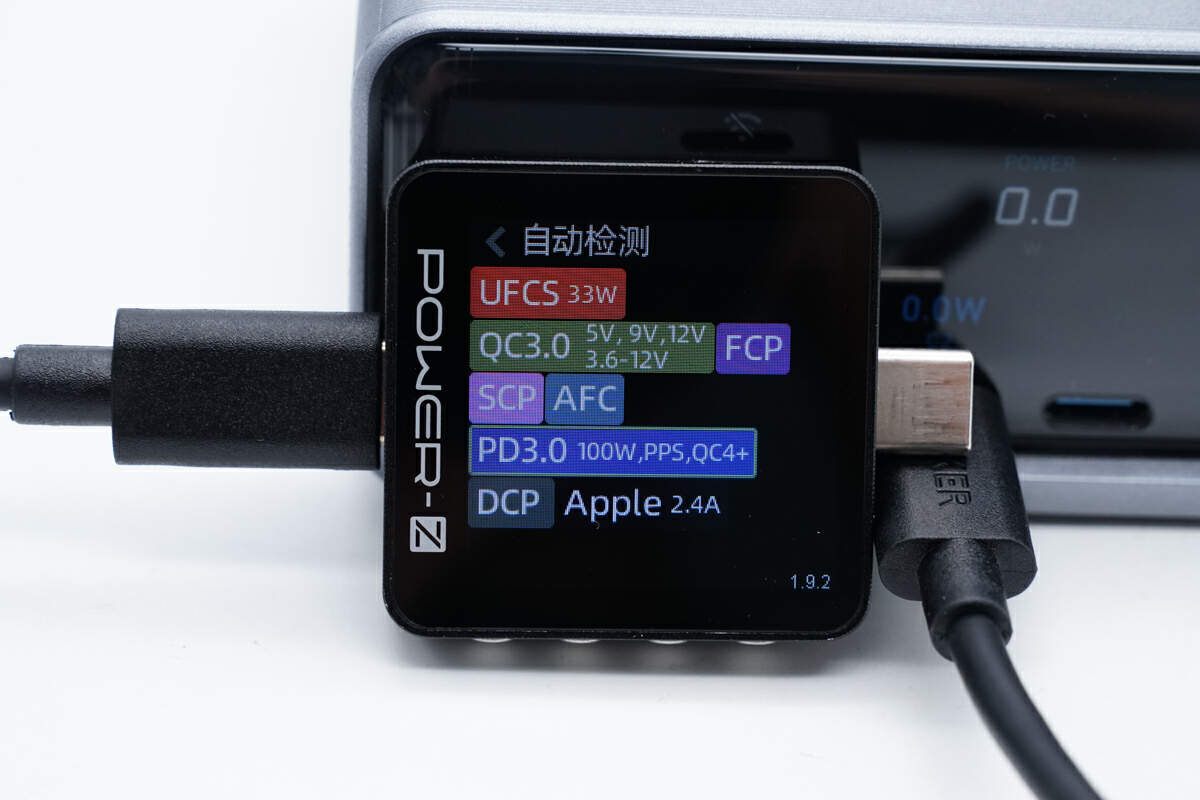
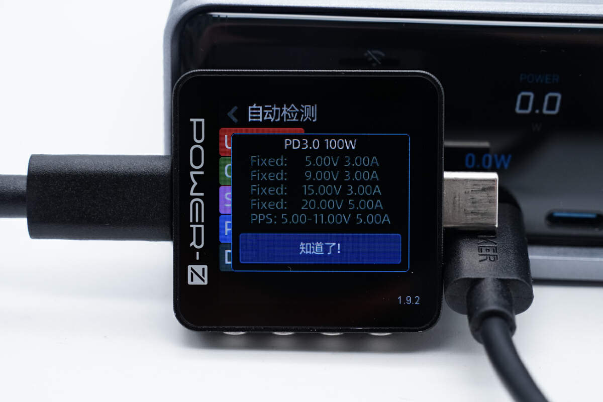
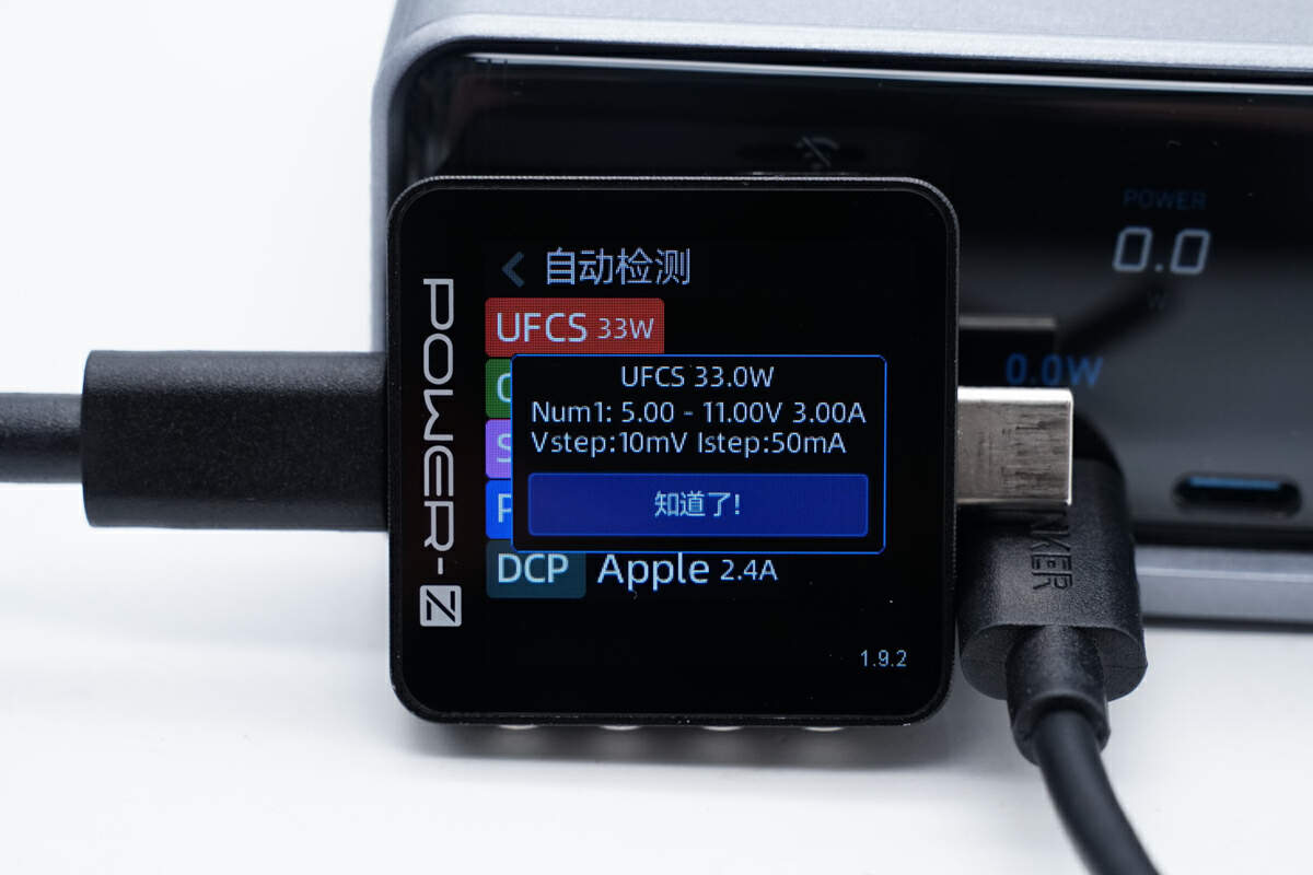
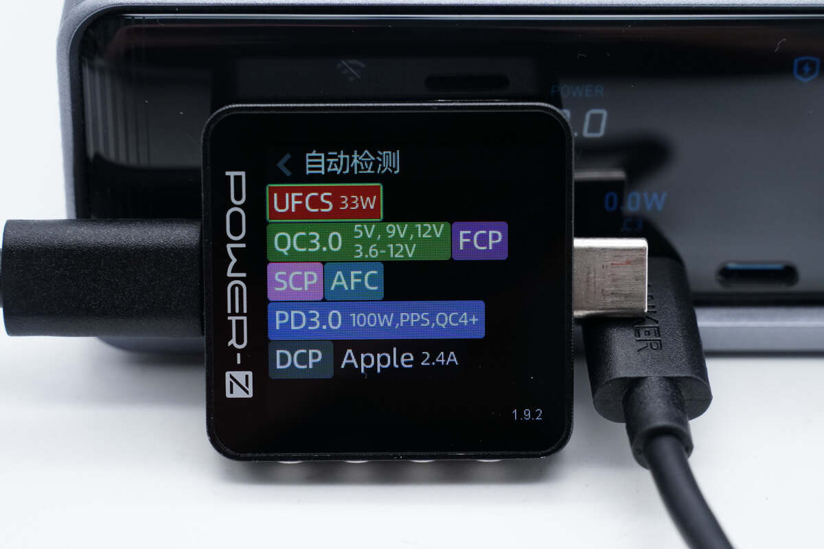
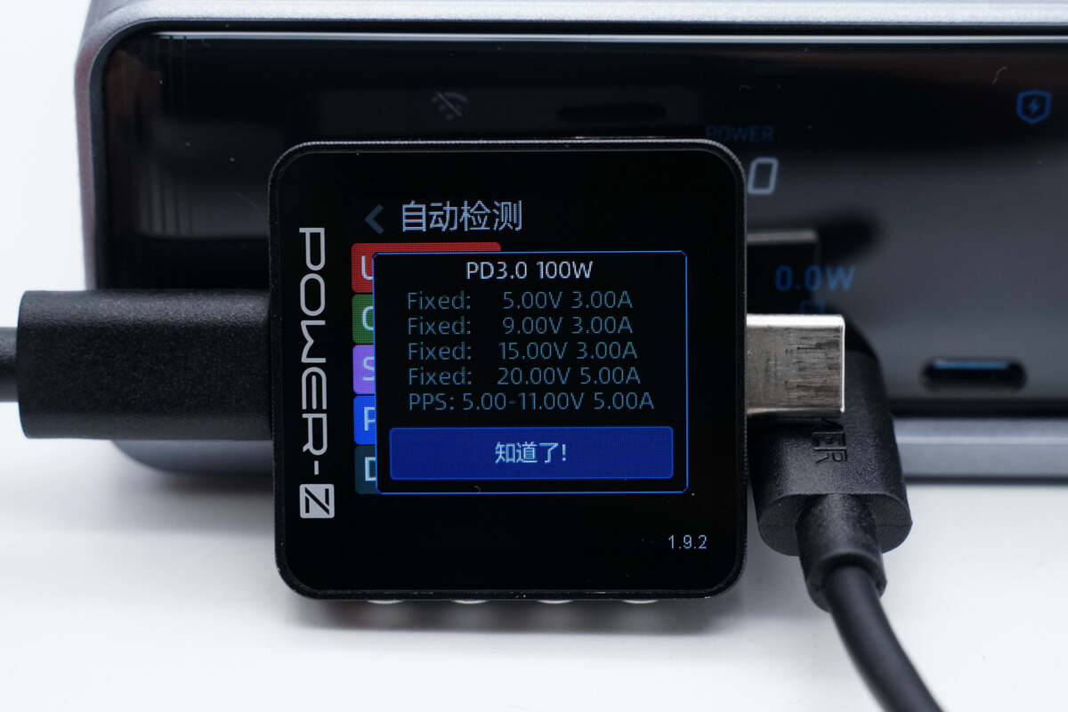
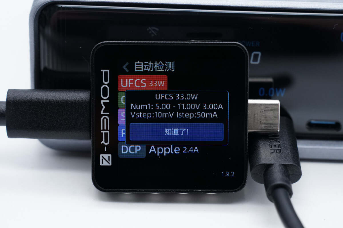
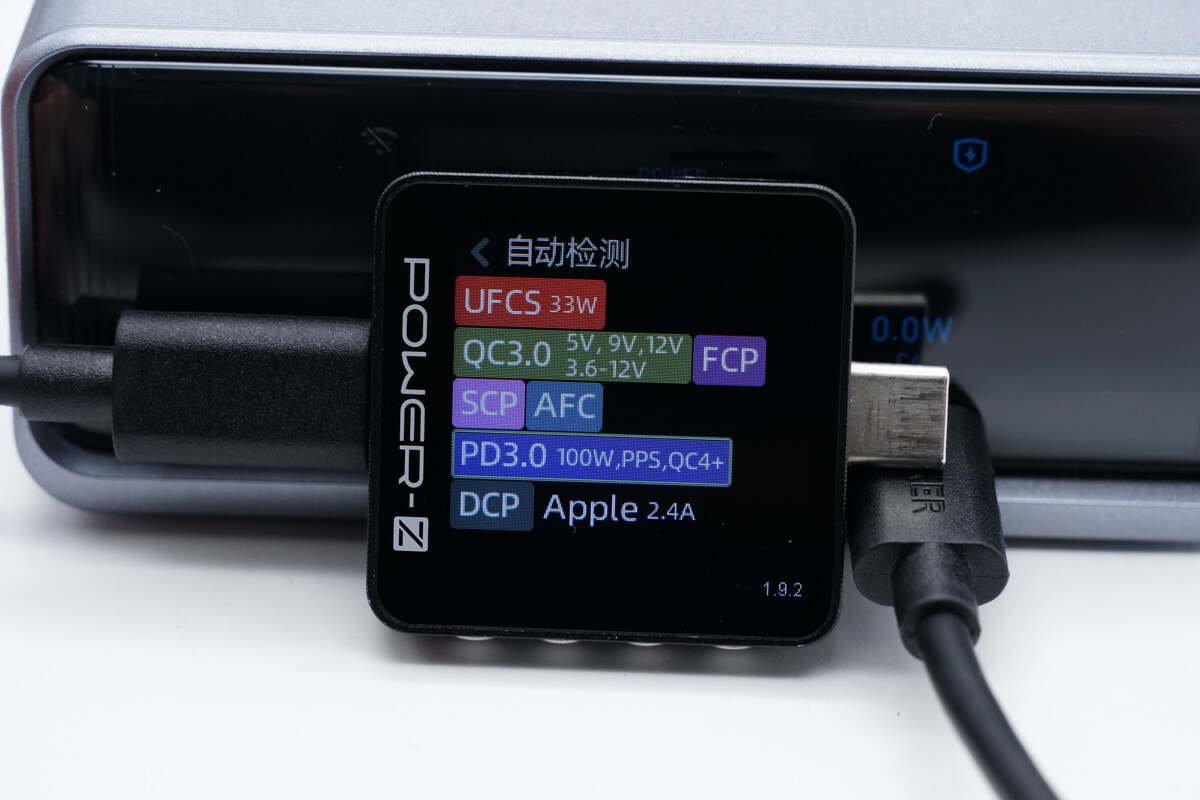
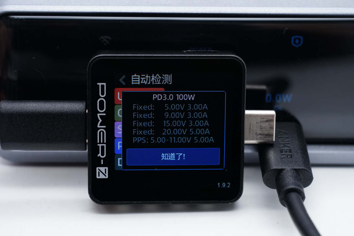
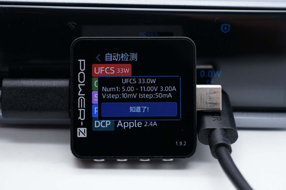
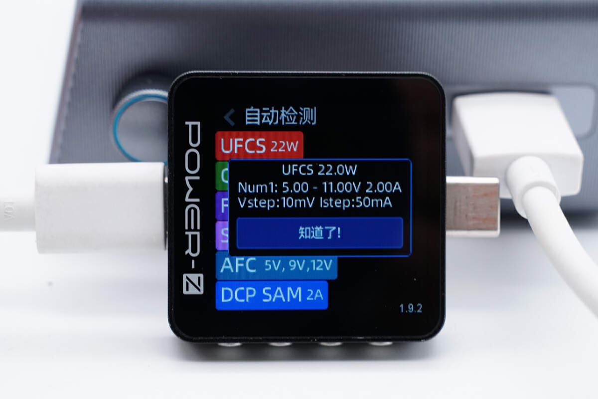
ChargerLAB POWER-Z KM003C shows the USB-C1 can support UFCS, QC3.0/4+, FCP, SCP, AFC, PD3.1, PPS, DCP, and Apple 2.4A charging protocols.
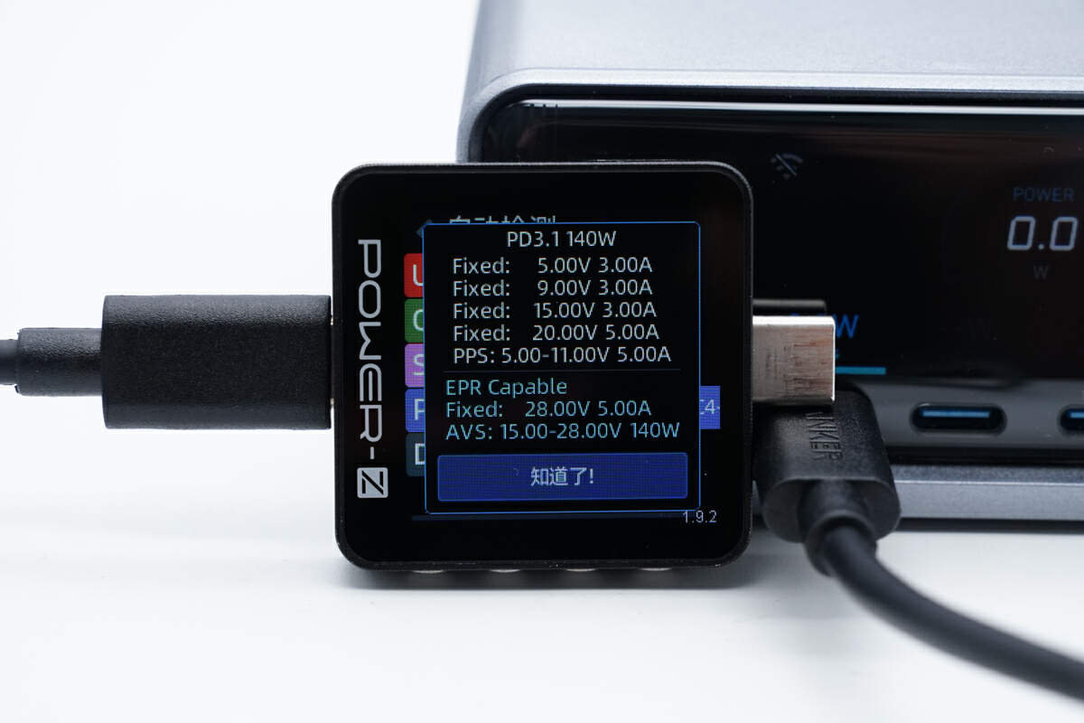
And it has five fixed PDOs of 5V/9V/15V3A and 20V/28V5A and a set of PPS, which is 5-11V5A. It also has a set of AVS, which is 15-28V 140W.
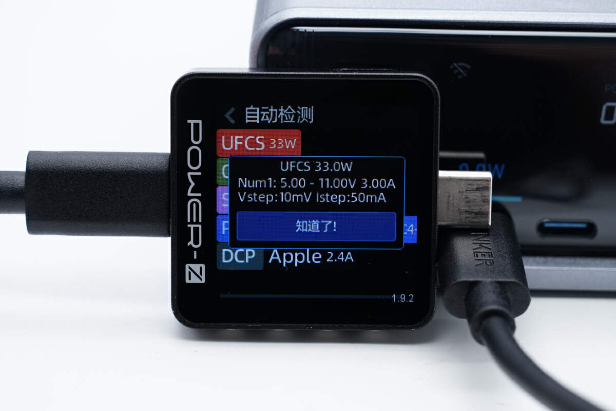
It can support UFCS of 5-11V3A.
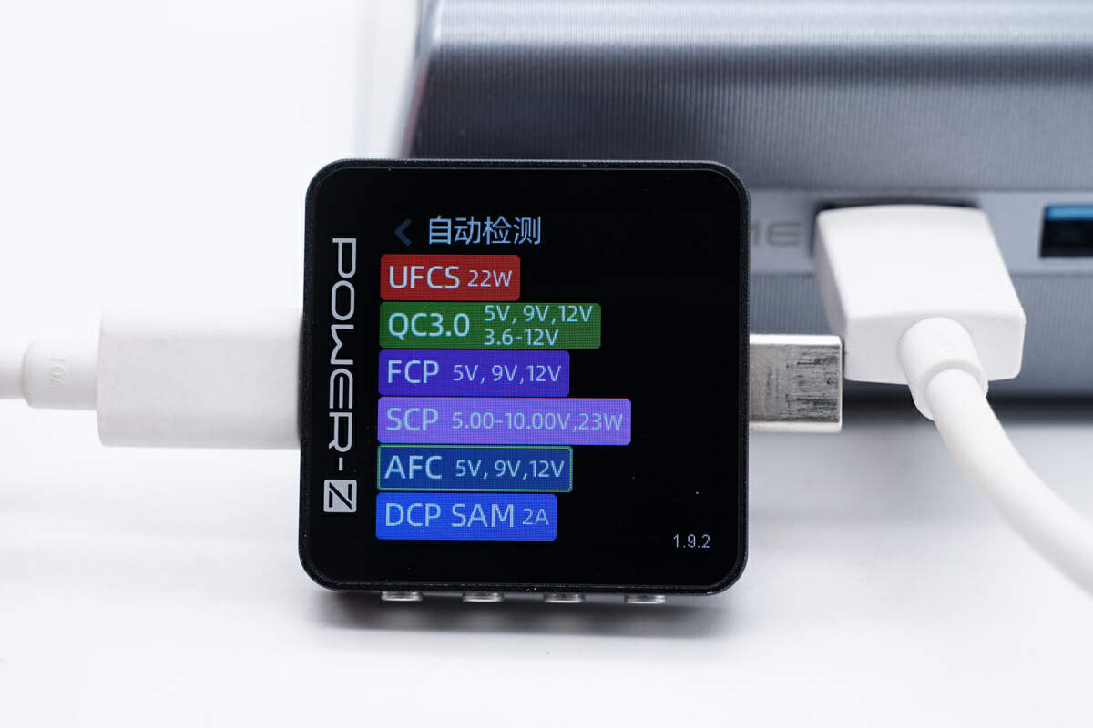
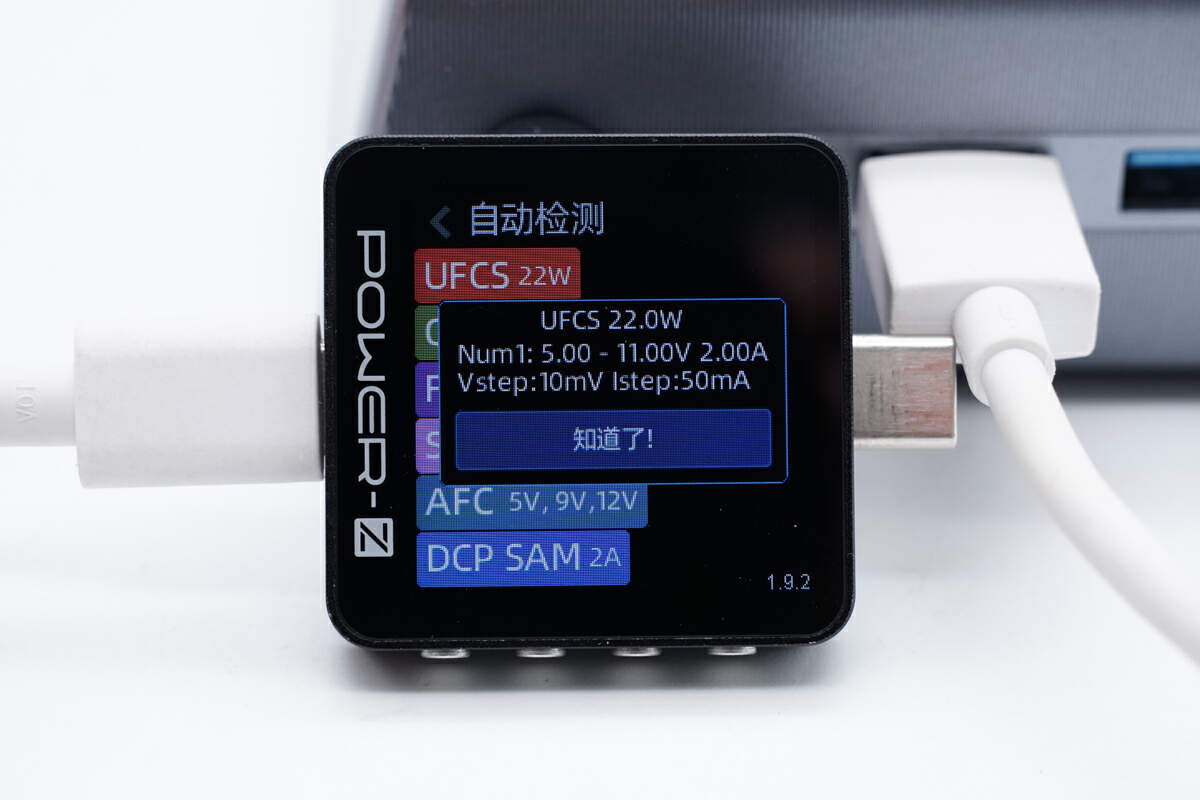
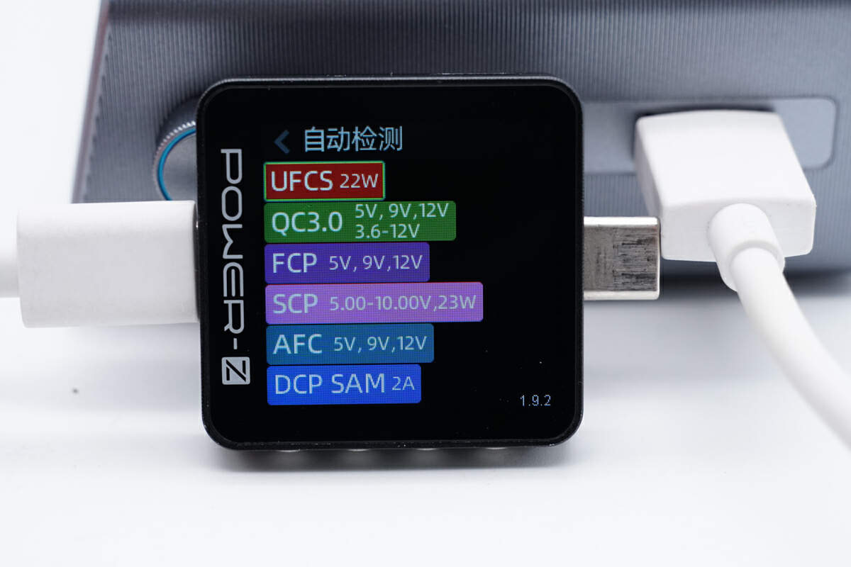
The USB-C2 supports UFCS, QC3.0/4+, FCP, SCP, AFC, PD3.0, PPS, DCP, and Apple 2.4A charging protocols.
And it has four fixed PDOs of 5V/9V/15V3A and 20V5A and a set of PPS, which is 5-11V5A.
It also supports UFCS of 5-11V3A.
The USB-C3 supports UFCS, QC3.0/4+, FCP, SCP, AFC, PD3.0, PPS, DCP, and Apple 2.4A charging protocols.
And it has four fixed PDOs of 5V/9V/15V3A and 20V5A and a set of PPS, which is 5-11V5A.
It also supports UFCS of 5-11V3A.
The USB-C4 supports the same protocols as USB-C2 and USB-C3.
So as the PDOs.
So as the UFCS.
The USB-A1 supports UFCS, QC3.0, FCP, SCP, AFC, DCP, and SAM 2A charging protocols.
It has a set of UFCS, which is 5-11V2A.
The USB-A2 supports the same protocols as USB-A1.
It has a set of UFCS, which is 5-11V2A.
Teardown
Next, let's take it apart to see its internal components and structure.
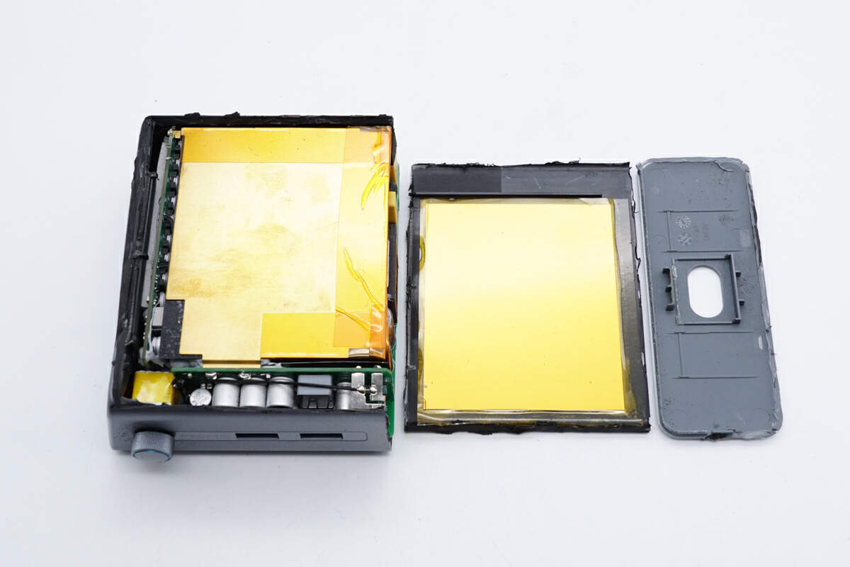
Cut away the input slot and the top side of the shell.
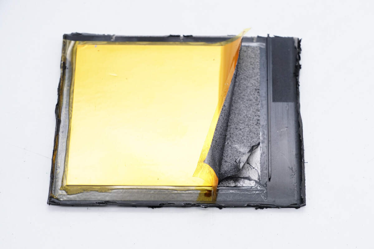
The top shell is covered with graphite sticker, copper foil, and insulating tape.
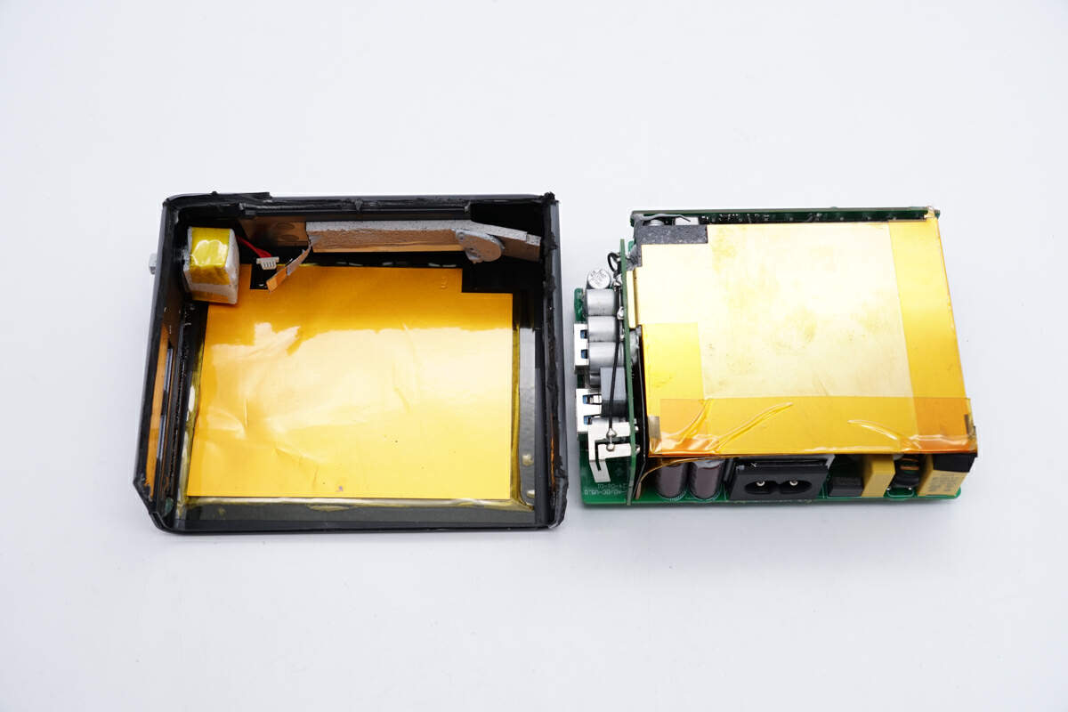
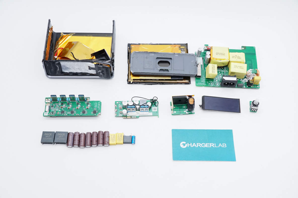
Take out the PCBA module, and the same heat dissipation design was made in the other part of the shell.
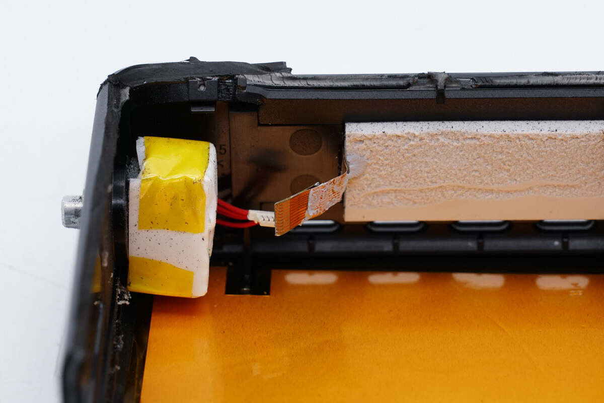
The alloy knob is covered with Mylar sheets and sponge and is connected to the PCBA module through pluggable wires. The screen is connected via a flat cable.
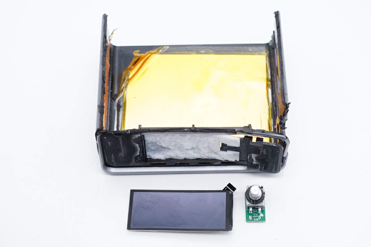
Remove the screen, and the corresponding area of the screen is covered with sponge for protection.
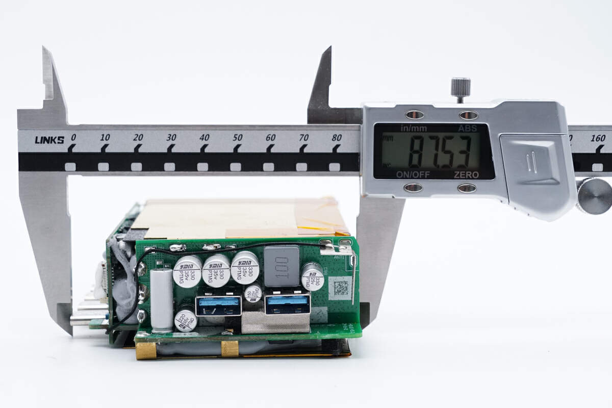
The length of the PCBA module is about 87.5 mm (3.44 inches).
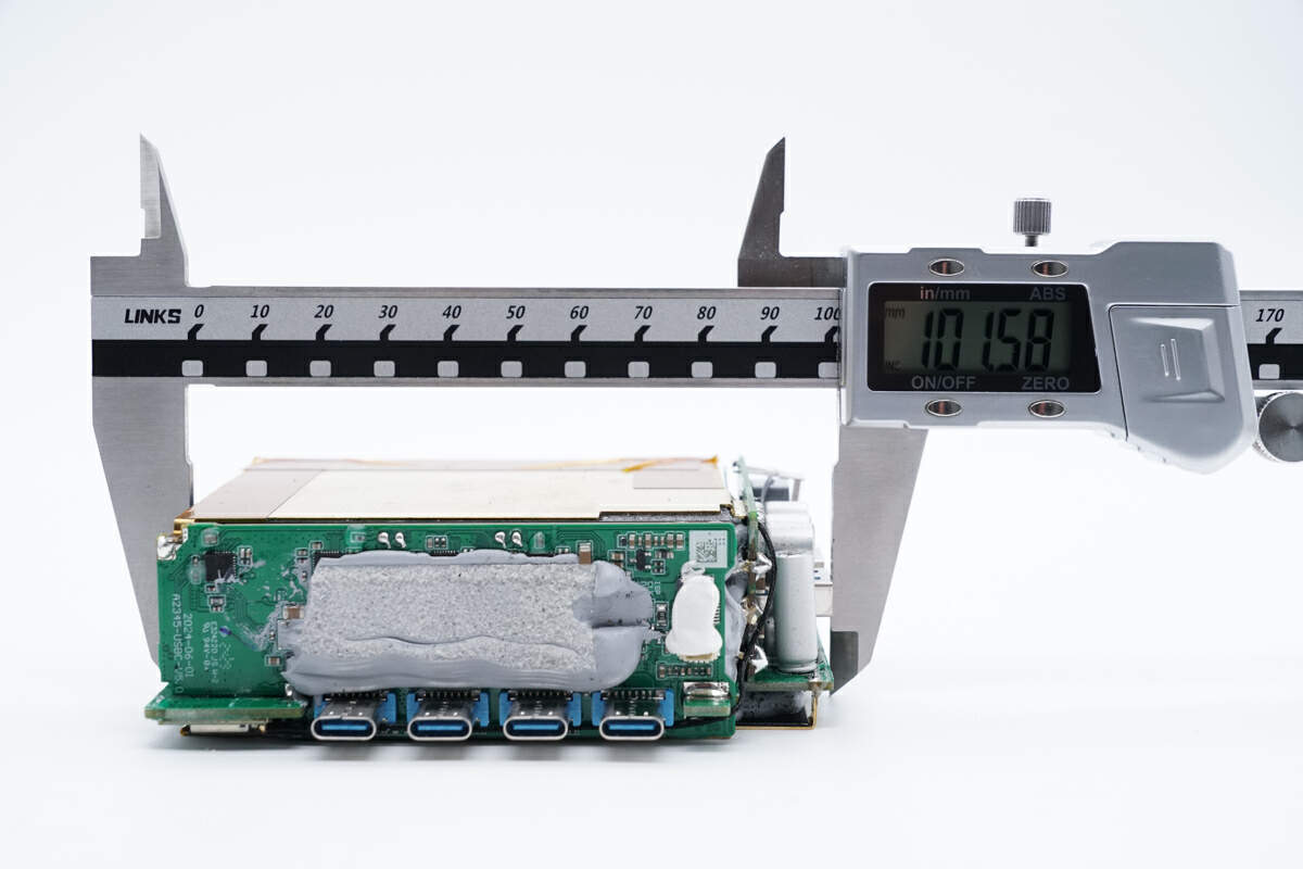
The width is about 101.6 mm (4 inches).
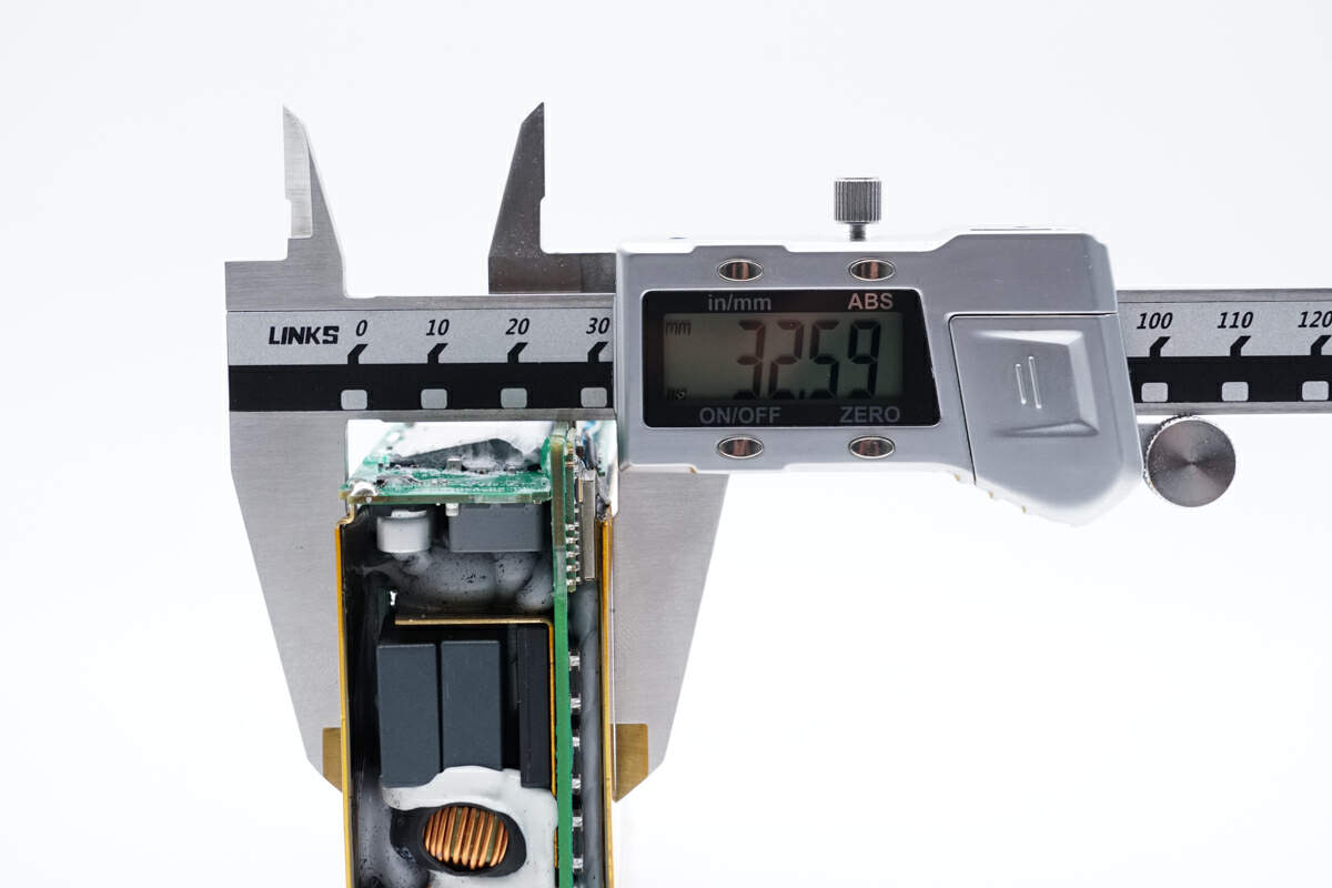
The thickness is about 32.6 mm (1.28 inches).
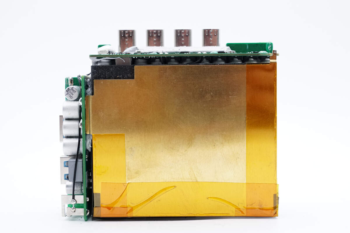
The top of the PCBA module is covered with a large brass heat sink.
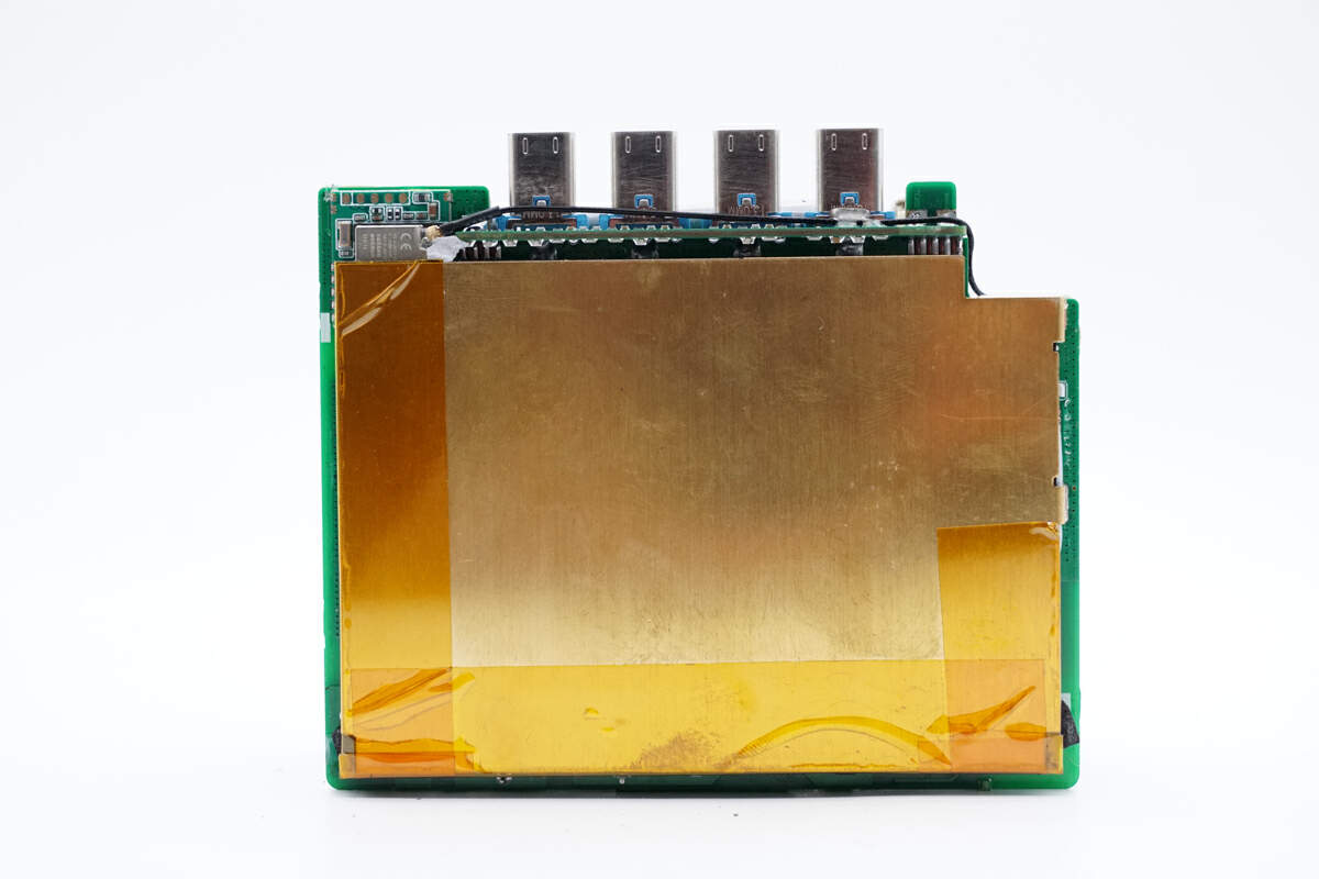
The bottom is also covered with a large area of brass heat sink, and the two heat sinks are fixed by soldering.
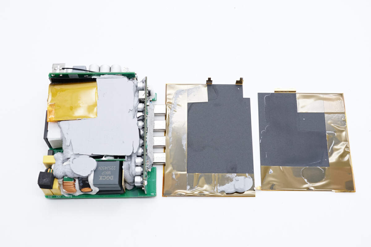
Remove the heat sink, and find the Mylar sheet on the inside for isolation and insulation and insulating tape on the edge.
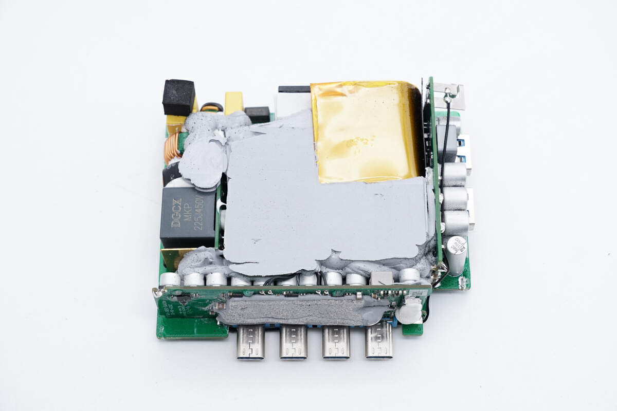
The components on the front of the PCBA module are reinforced by potting compound, Mylar sheets isolate the back of the small PCB on the right, and the upper right corner is covered with graphite heat dissipation stickers.
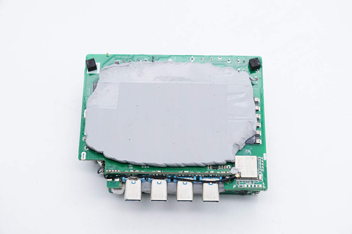
The back of the PCBA module is also covered with potting compound.
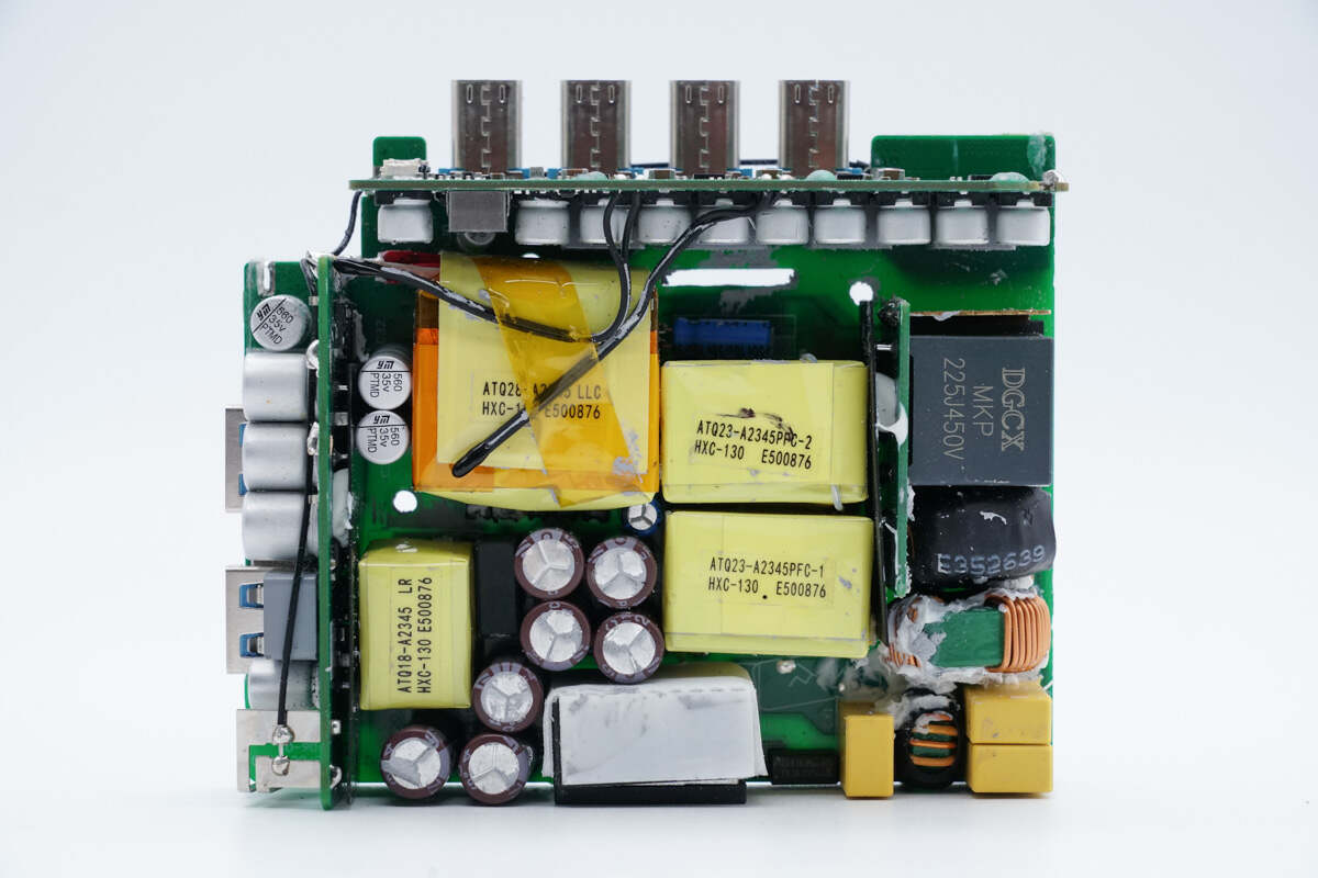
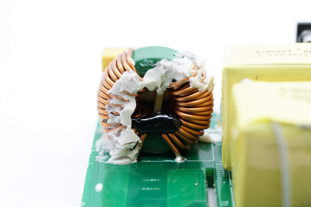
Clean up the potting compound. There are the PFC boost inductor, electrolytic capacitor, resonant capacitor, resonant inductor, transformer, and thermistor on the front.
There are the bridge rectifier, PFC controller, PFC MOSFET, PFC rectifier, LLC controller, LLC half-bridge MOSFET, optocoupler, and other components on the back.
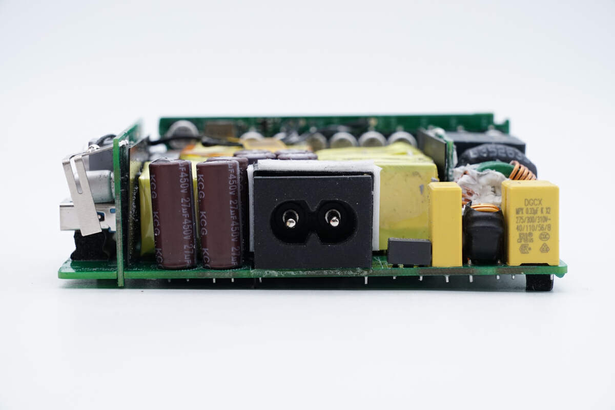
The right side of this side has the time-delay fuse, safety X2 capacitor, and common mode choke.
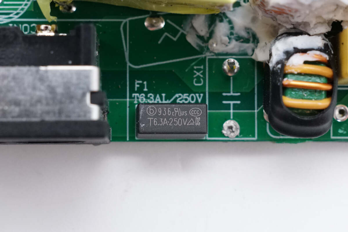
The time-delay fuse is from Betterfuse. 6.3A 250V.
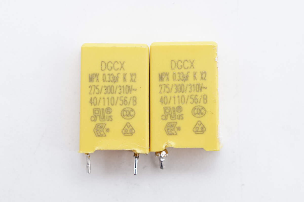
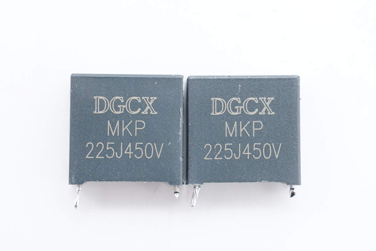
These two safety X2 capacitors are from DGCX. 0.33μF.
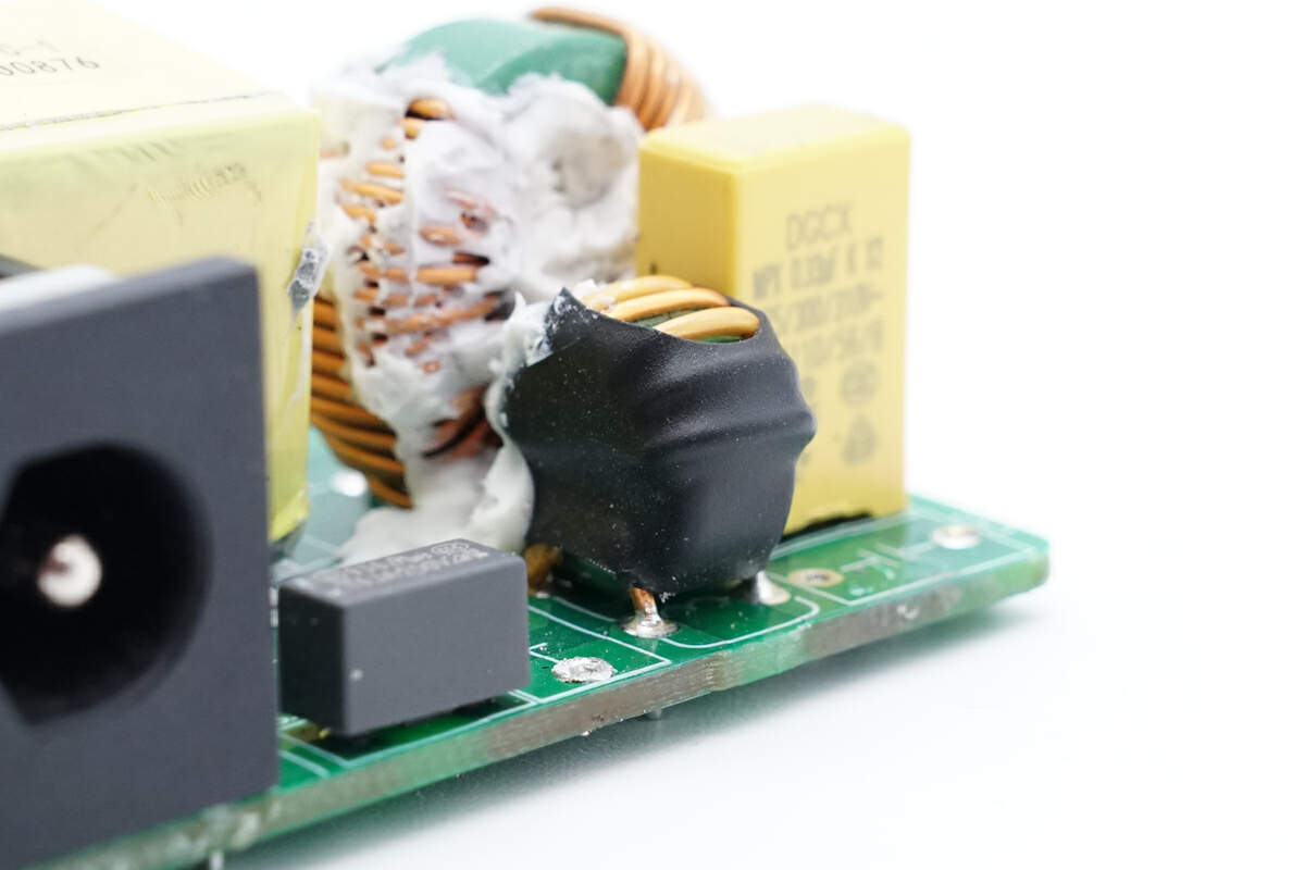
The common mode choke is insulated by heat-shrinkable tubing.
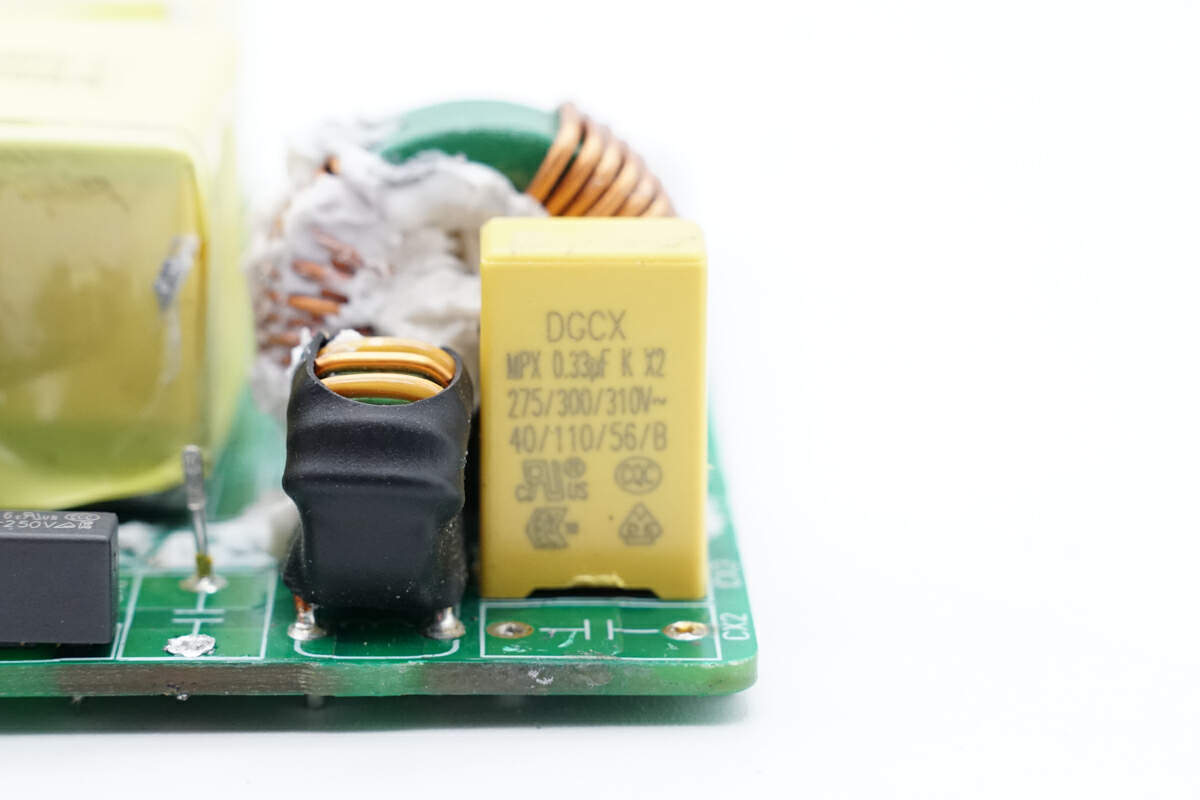
The third safety X2 capacitor is also from DGCX. 0.33μF.
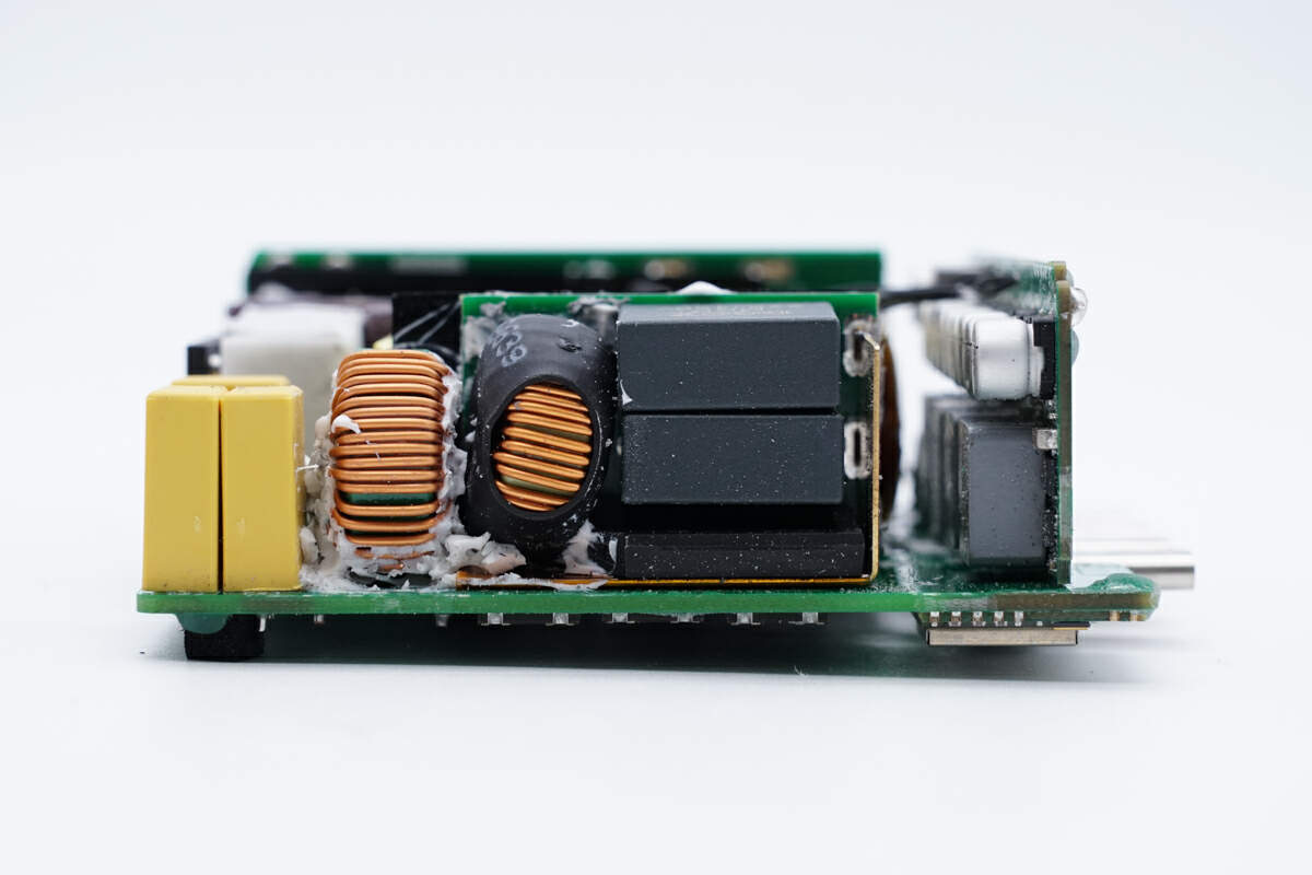
The other side is equipped with common mode choke, bridge rectifier, filter inductor, and filter capacitor.
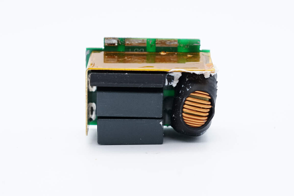
The bridge rectifier, filter inductor, and filter capacitor are soldered on a separate small PCB. The bridge rectifier is equipped with a brass heat sink to help dissipate heat.
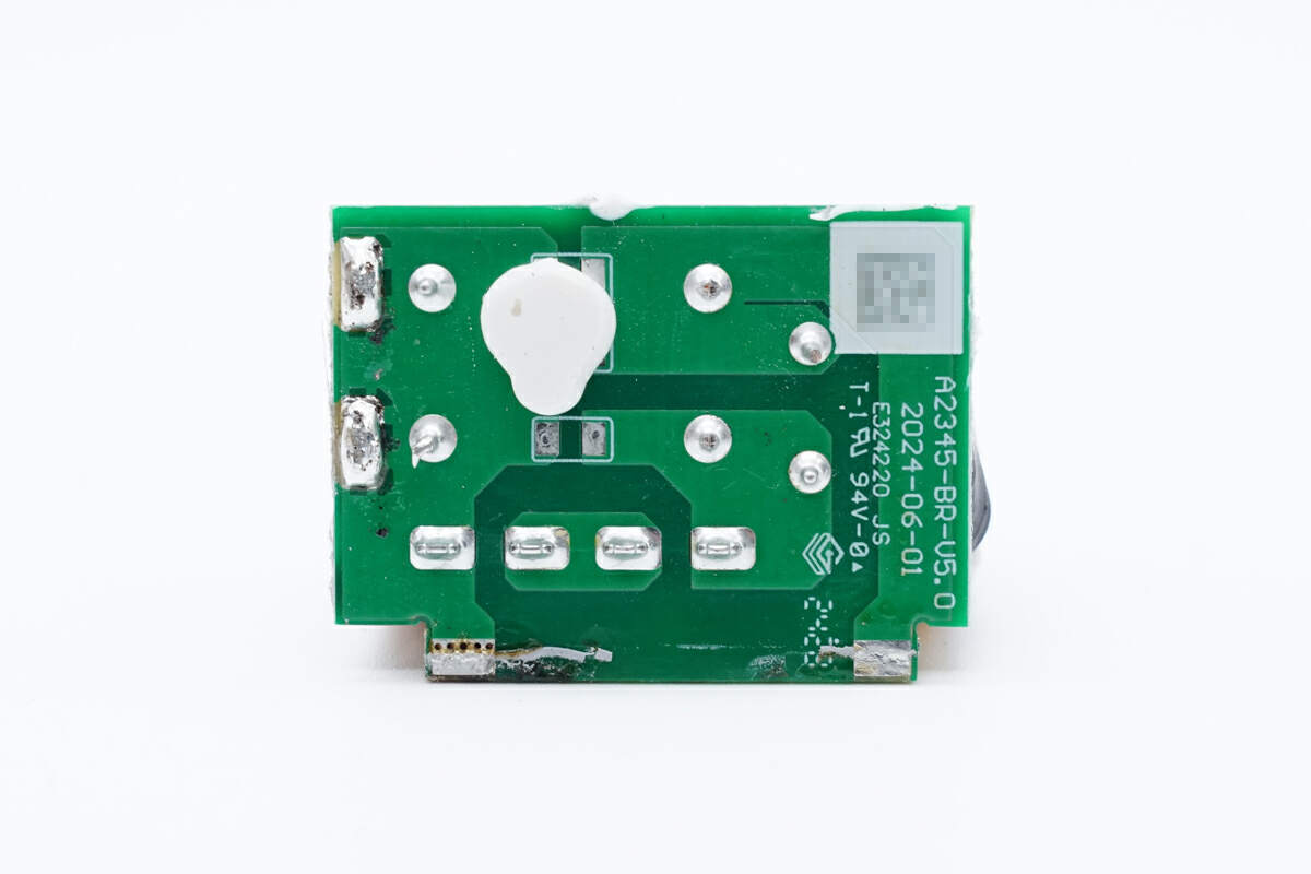
There are no components on the back of this small PCB.
Two secondary common mode chokes are used to filter out EMI interference.
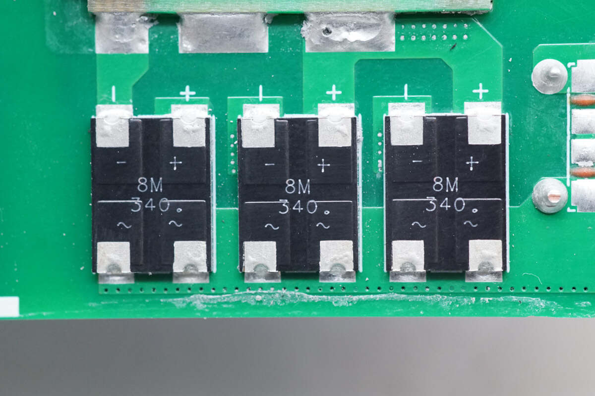
The other three bridge rectifiers on the back of the PCBA module are all marked with 8M340.
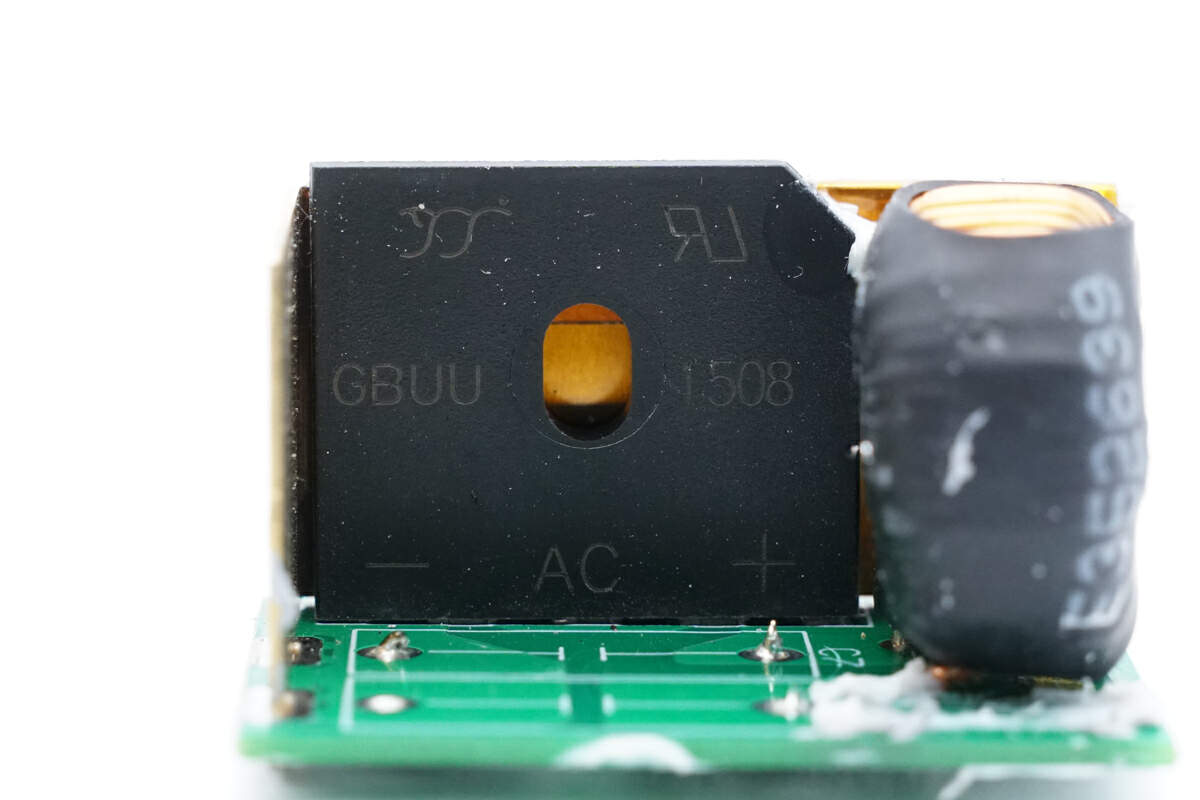
The bridge rectifier is from YJ and adopts GBU package. 15A 800V. Model is GBUU1508.
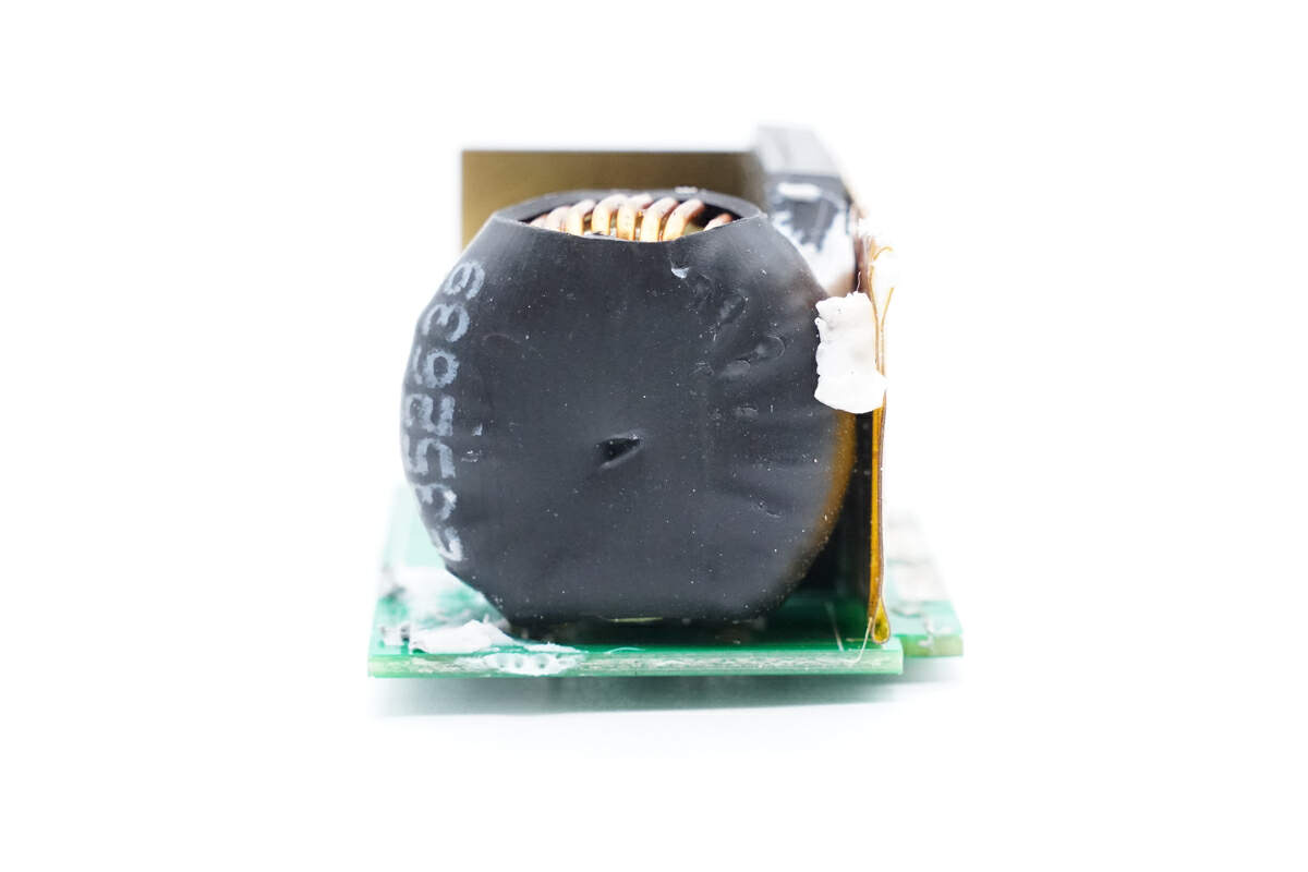
The filter inductor jacket heat-shrinkable tubing.
These two filter capacitors are also from DGCX. 2.2μF 450V.
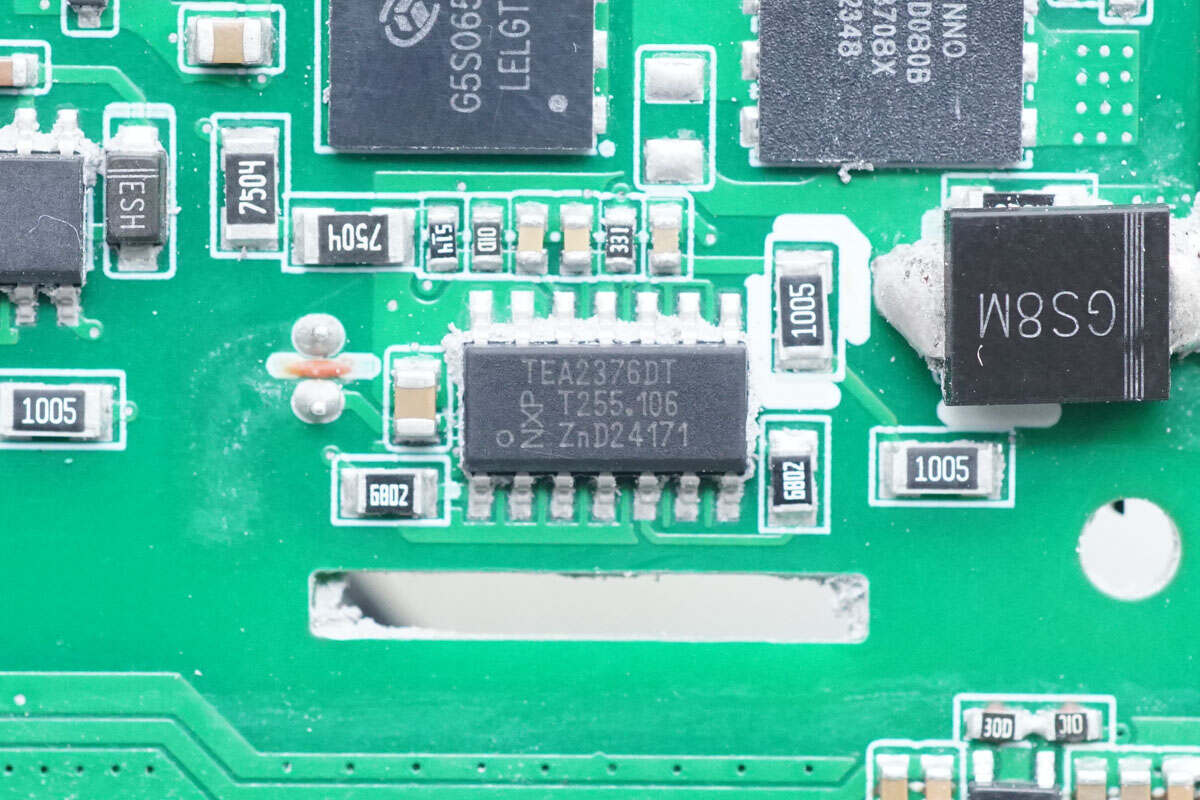
The PFC controller is from NXP and adopts SO14 package. It is a digitally configurable two-phase interleaved PFC controller that supports DCM or QR operation mode. The chip has multiple protection functions. Model is TEA2376DT.
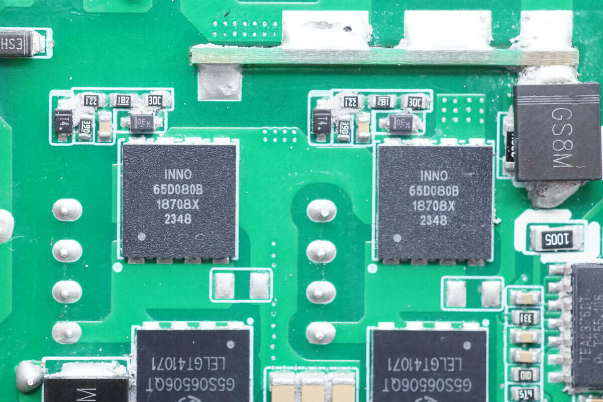
These two PFC boost MOSFETs are from Innoscience. It is an enhancement-mode GaN FET with a withstand voltage of 650V and, a transient withstand voltage of 800V and a conduction resistance of 80mΩ. It supports ultra-high switching frequency, has no reverse recovery charge, has extremely low gate charge and output charge, meets the industrial application requirements of JEDEC standards, has built-in ESD protection, and complies with RoHS, lead-free and EU REACH regulations. Model is INN650D080B.
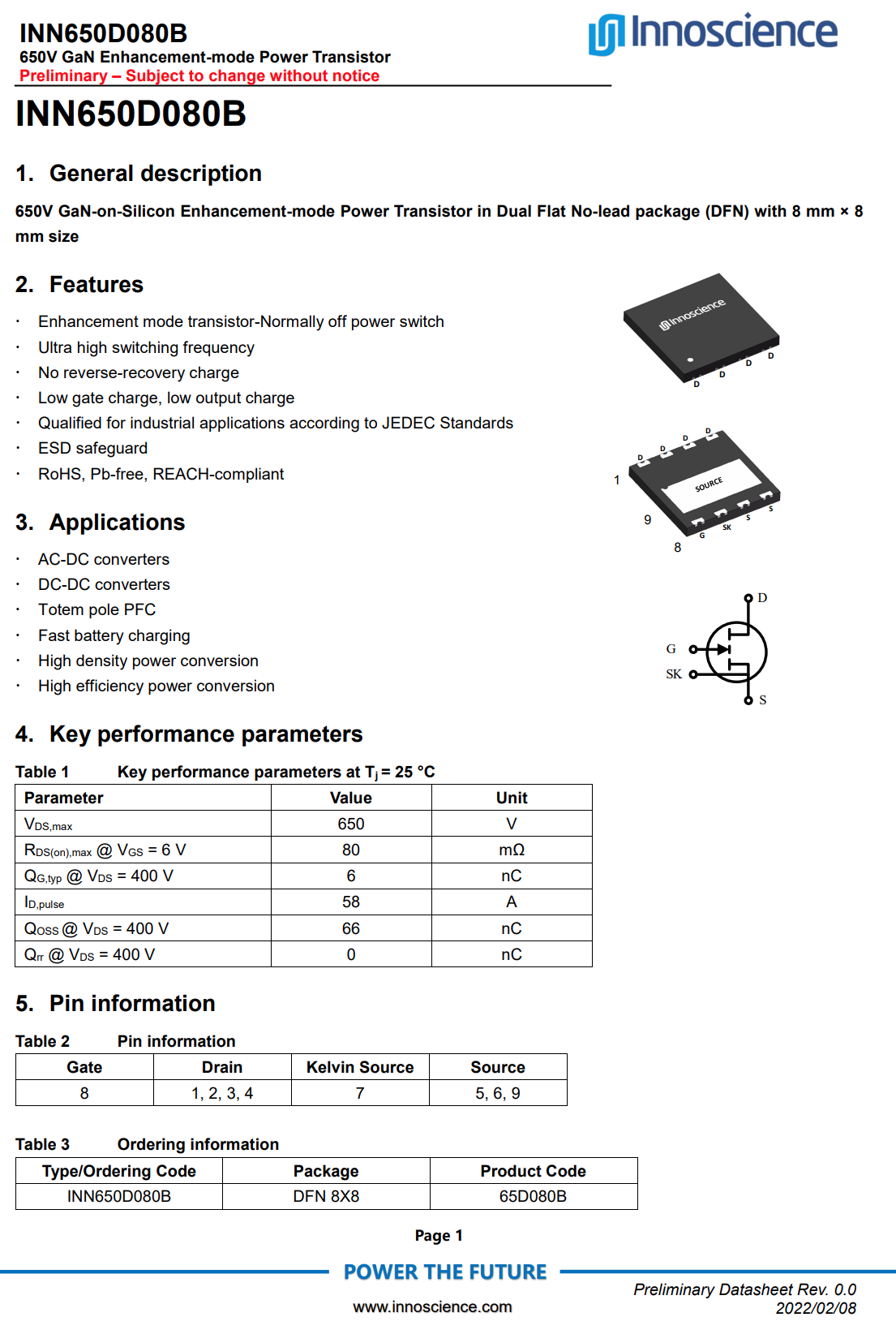
There is the information about Innoscience INN650D080B.
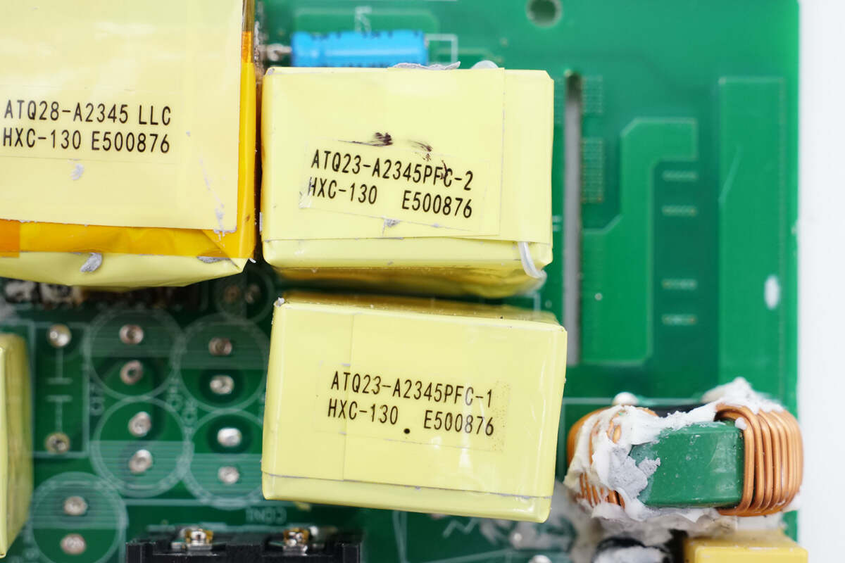
The two PFC boost inductors use ATQ23 magnetic cores and are insulated by tape.
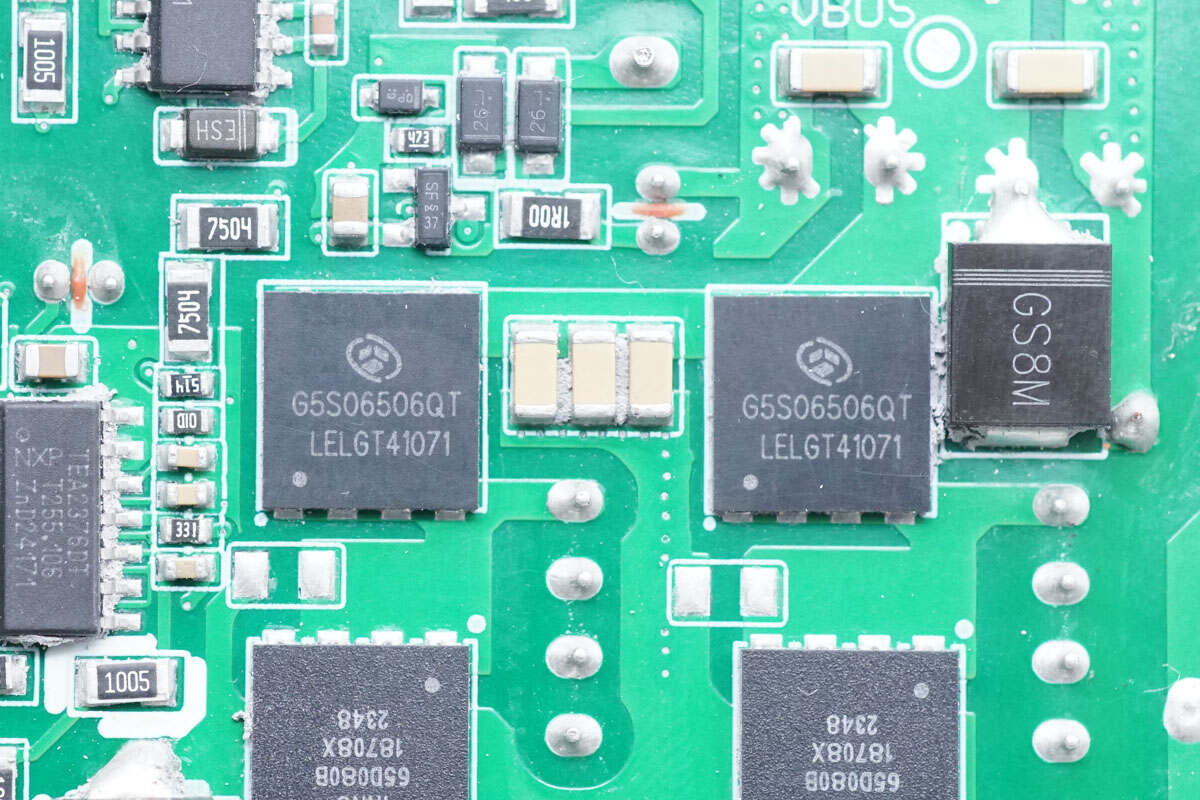
These two PFC rectifiers are from GlobalPower and adopt DFN8*8 package. This is a silicon carbide diode with a withstand voltage of 650V, an operating current of 6A at 136℃, and a maximum operating temperature of 150℃. Model is G5S06506QT.
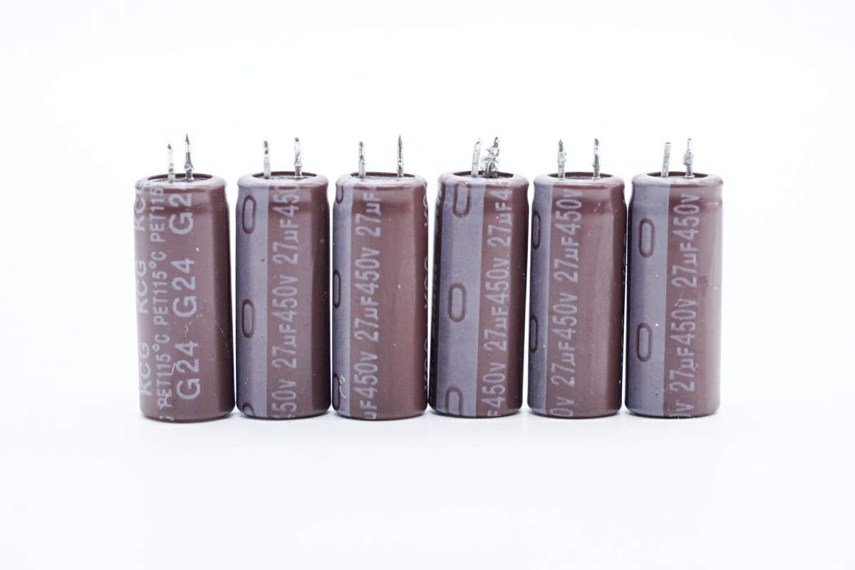
The electrolytic capacitors are from the YMIN KCG series. This series has outstanding advantages in voltage resistance and life span and maintains characteristics such as lightning resistance, low leakage, high ripple resistance, and high-frequency resistance, making it more suitable for the development of high-quality GaN fast charging chargers. 450V 27μF.
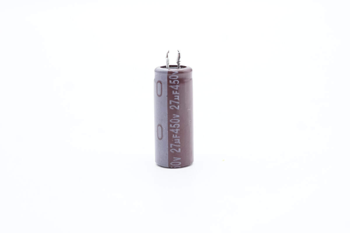
There is another one with the same specification of 450V 27μF.
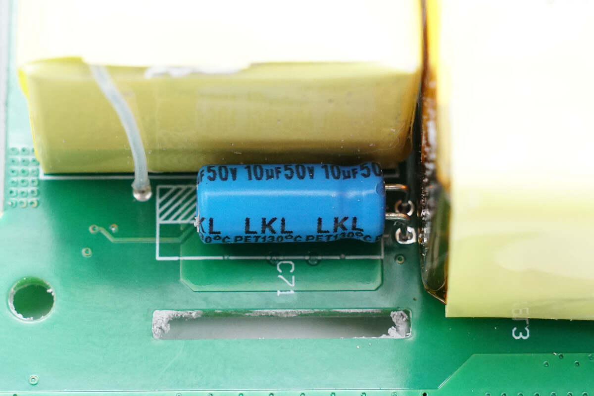
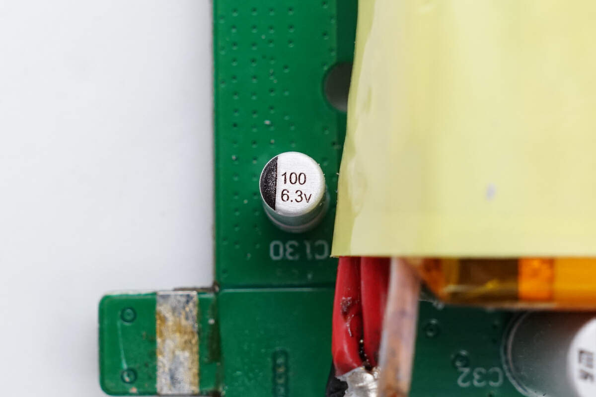
This is the capacitor that powers the master control chip. 50V10μF.
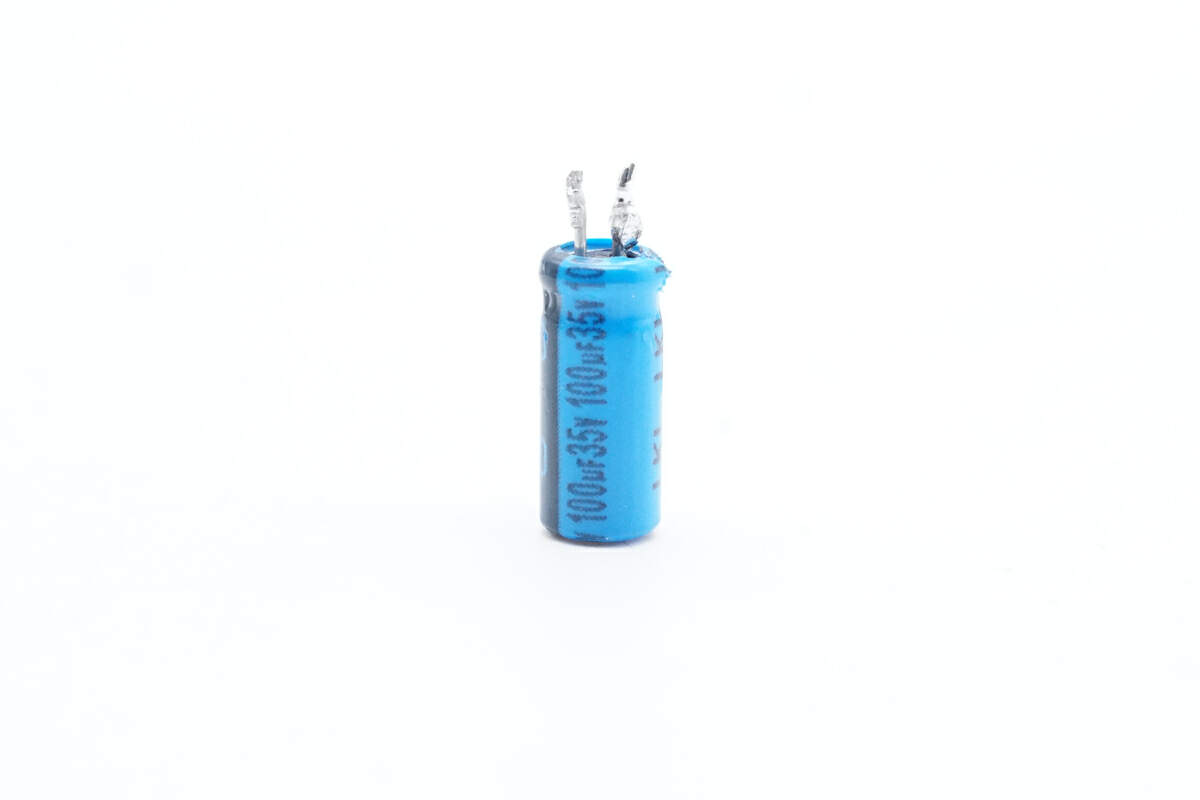
The other one has specifications of 35V 100μF.
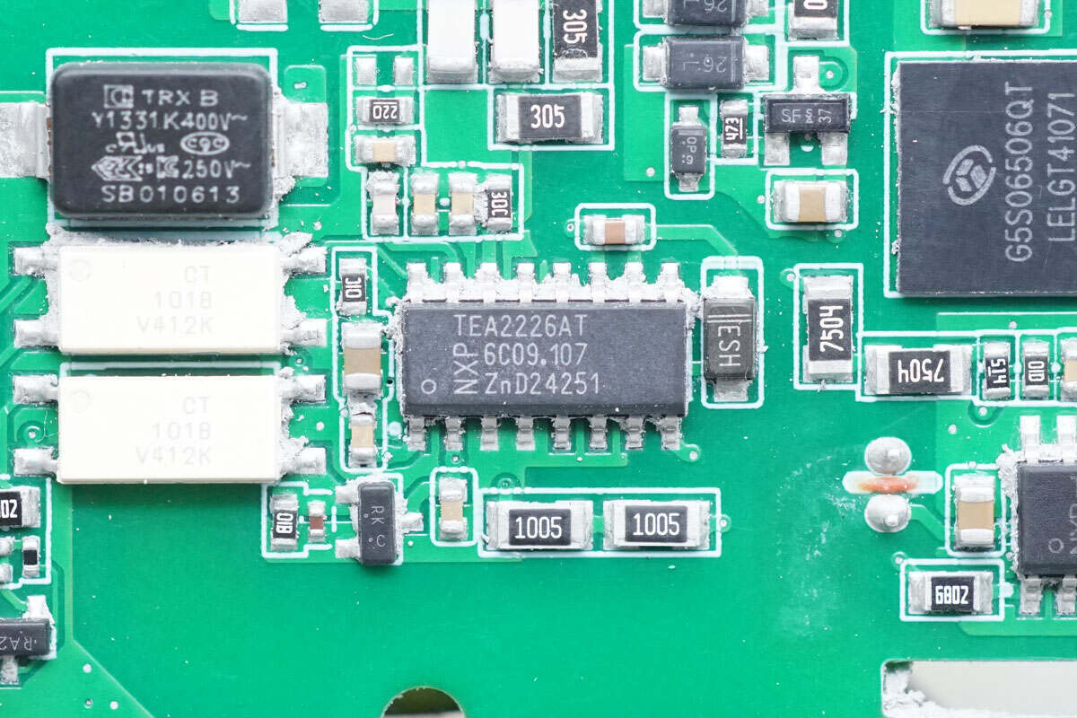
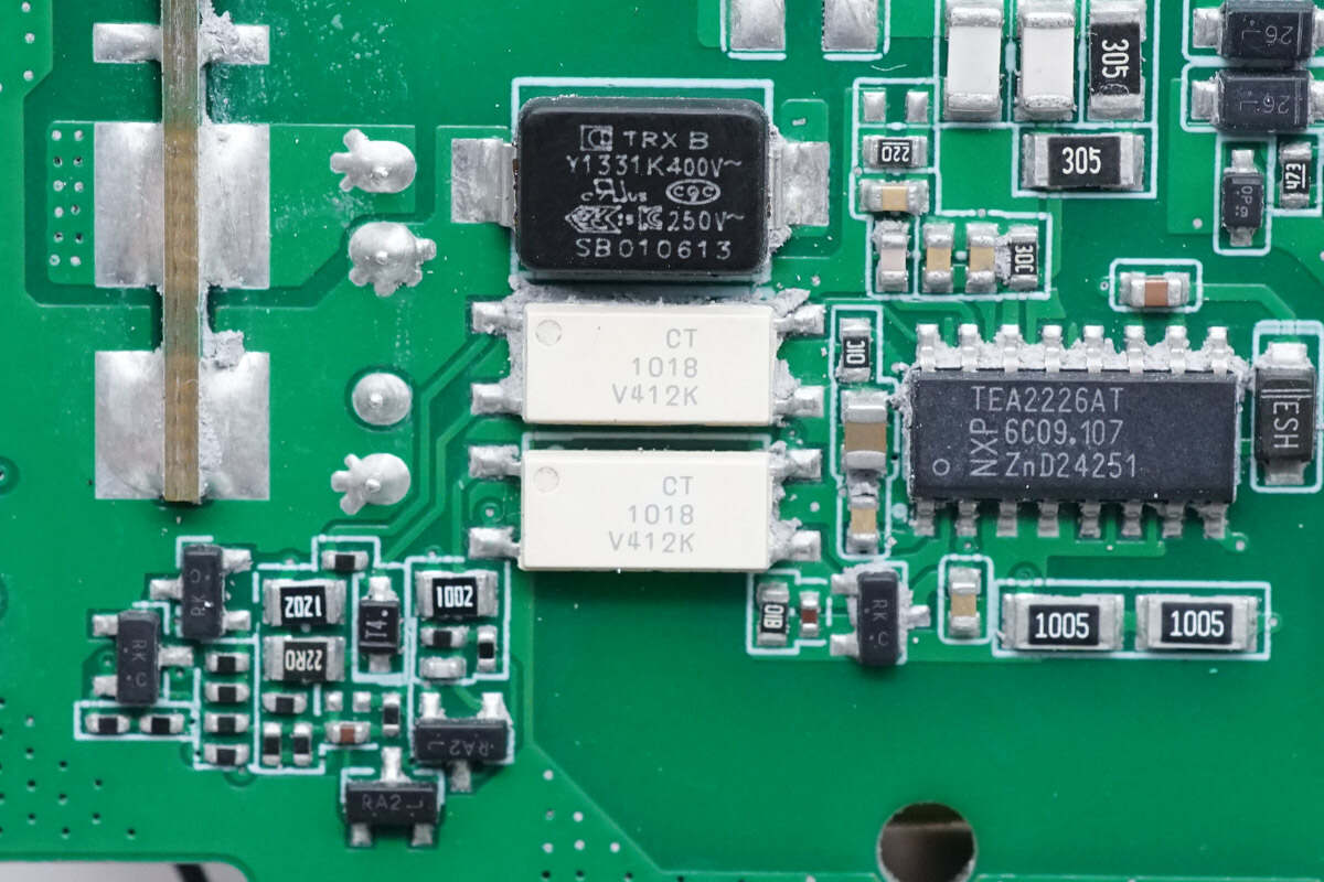
The LLC controller is from NXP and adopts SO16 package. It is a digitally configurable controller with integrated high-voltage startup and X-capacitor discharge, an internal integrated driver, and supports parameter configuration through a graphical user interface. It supports a variety of configurable protection functions and has excellent no-load power consumption. Model is TEA2226AT.
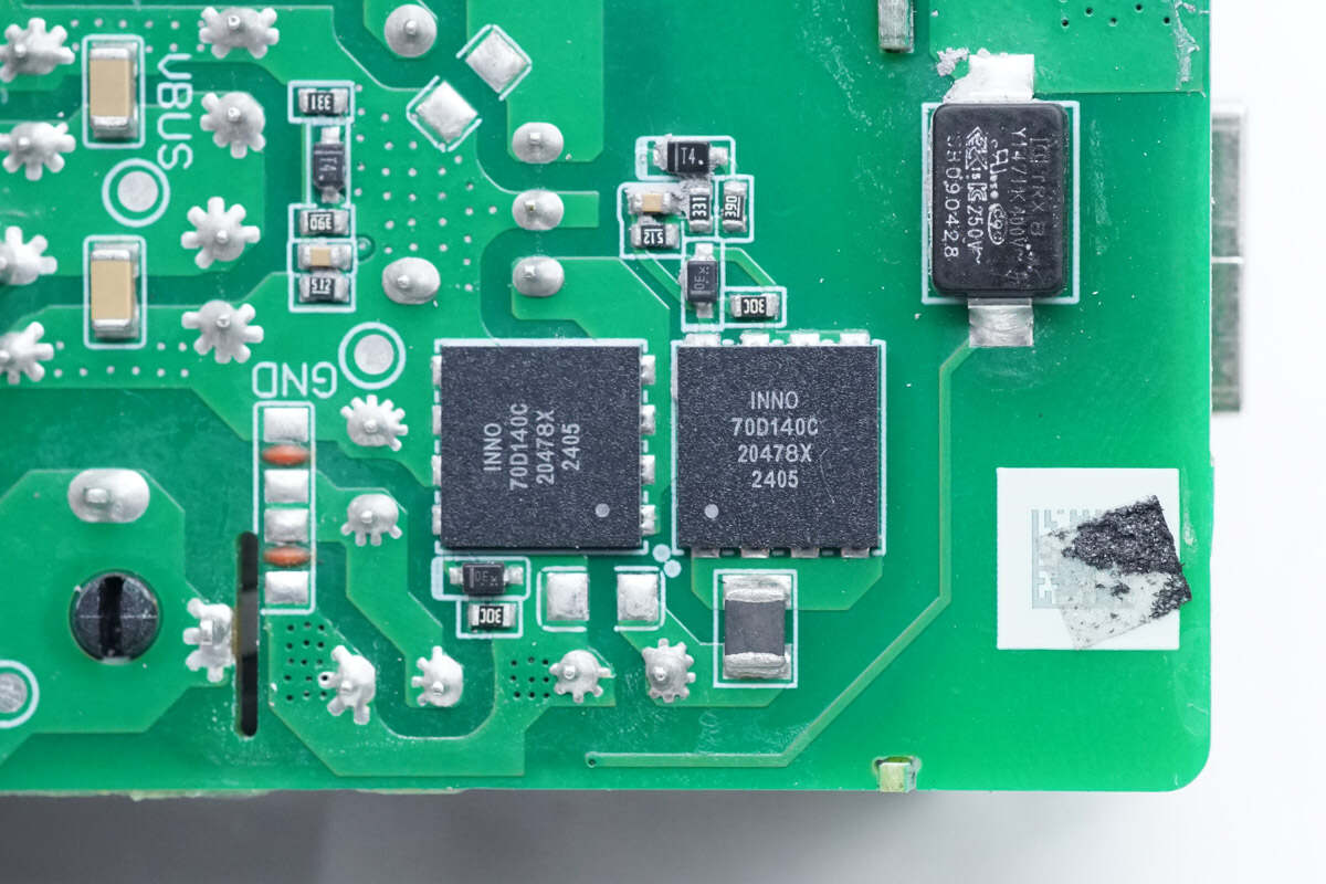
The two GaN FETs of the LLC half-bridge are from Innoscience and adopt DFN8*8 package. It is an enhancement-mode GaN FET with a withstand voltage of 700V, a conduction resistance of 140mΩ, and a Kelvin source. It has extremely low gate charge and output charge, meets the industrial application requirements of JEDEC standards, has built-in ESD protection, and complies with RoHS, lead-free, and EU REACH regulations. It is suitable for totem pole PFC, fast charging power supply, high power density, and high-efficiency switching power supply applications. Model is INN700D140C.
There is the information about Innoscience INN700D140C.
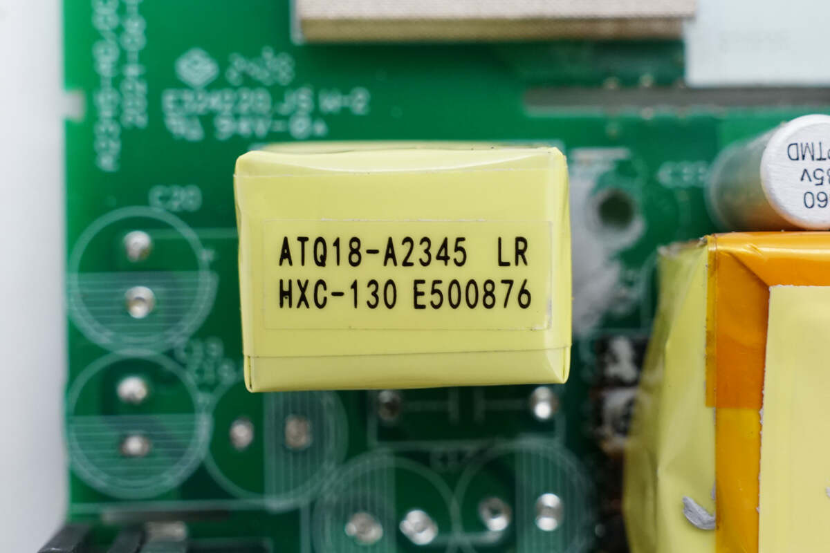
The resonant inductor adopts the ATQ18 magnetic core.
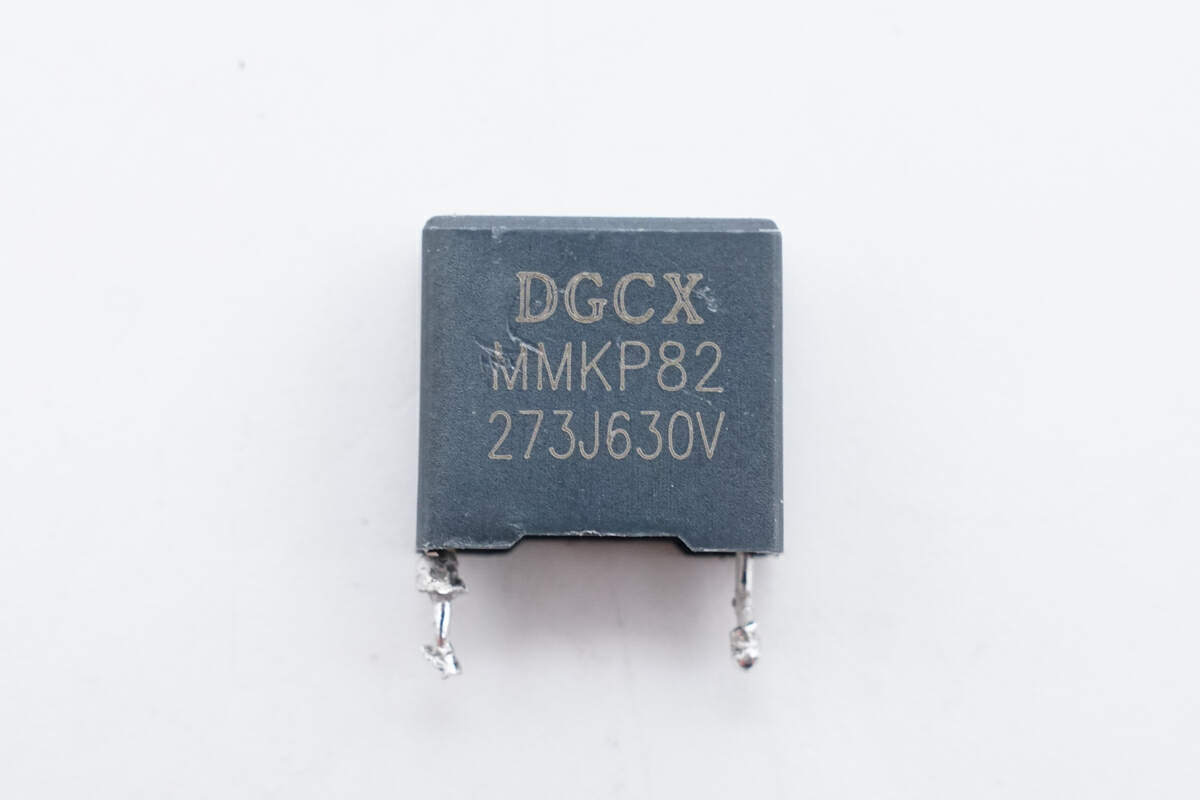
The resonant capacitor is from DGCX. 0.027μF 630V.
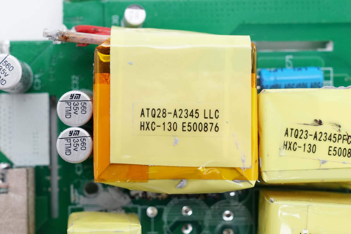
The LLC transformer adopts the ATQ28 magnetic core.
These two optocouplers are used for output voltage feedback and protection.
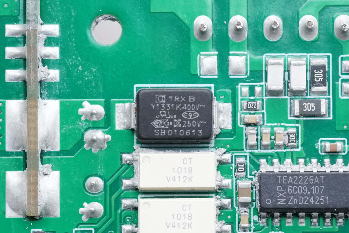
The SMD Y capacitor is from TRX. Its small size and light weight are suitable for high-density power products such as GaN fast chargers. The part number is TMY1331K.
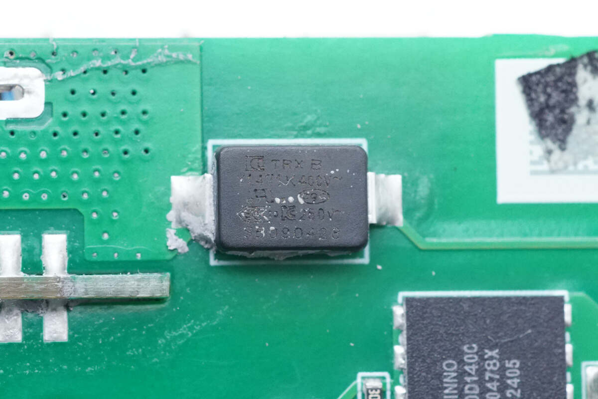
Another SMD Y capacitor is also from TRX, part number TMY1471K.
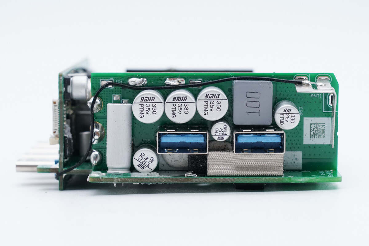
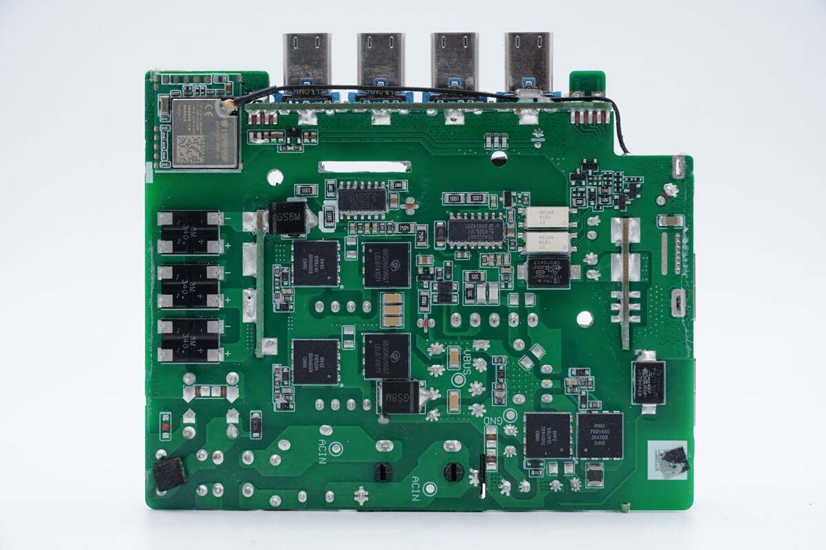
A small PCB of synchronous rectification is soldered on this side of the PCBA module. There is a buck inductor, multiple solid capacitors, and a USB-A socket on the front. The small PCB is connected to the wireless communication module on the back of the PCBA via a black wire.
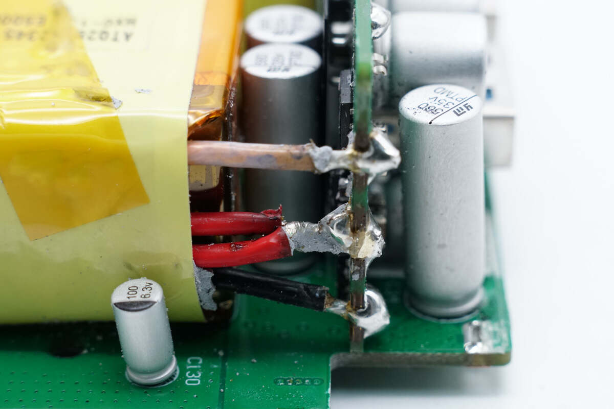
The transformer's secondary side is wound with Litz wire and connected to the PCB of synchronous rectification by soldering.
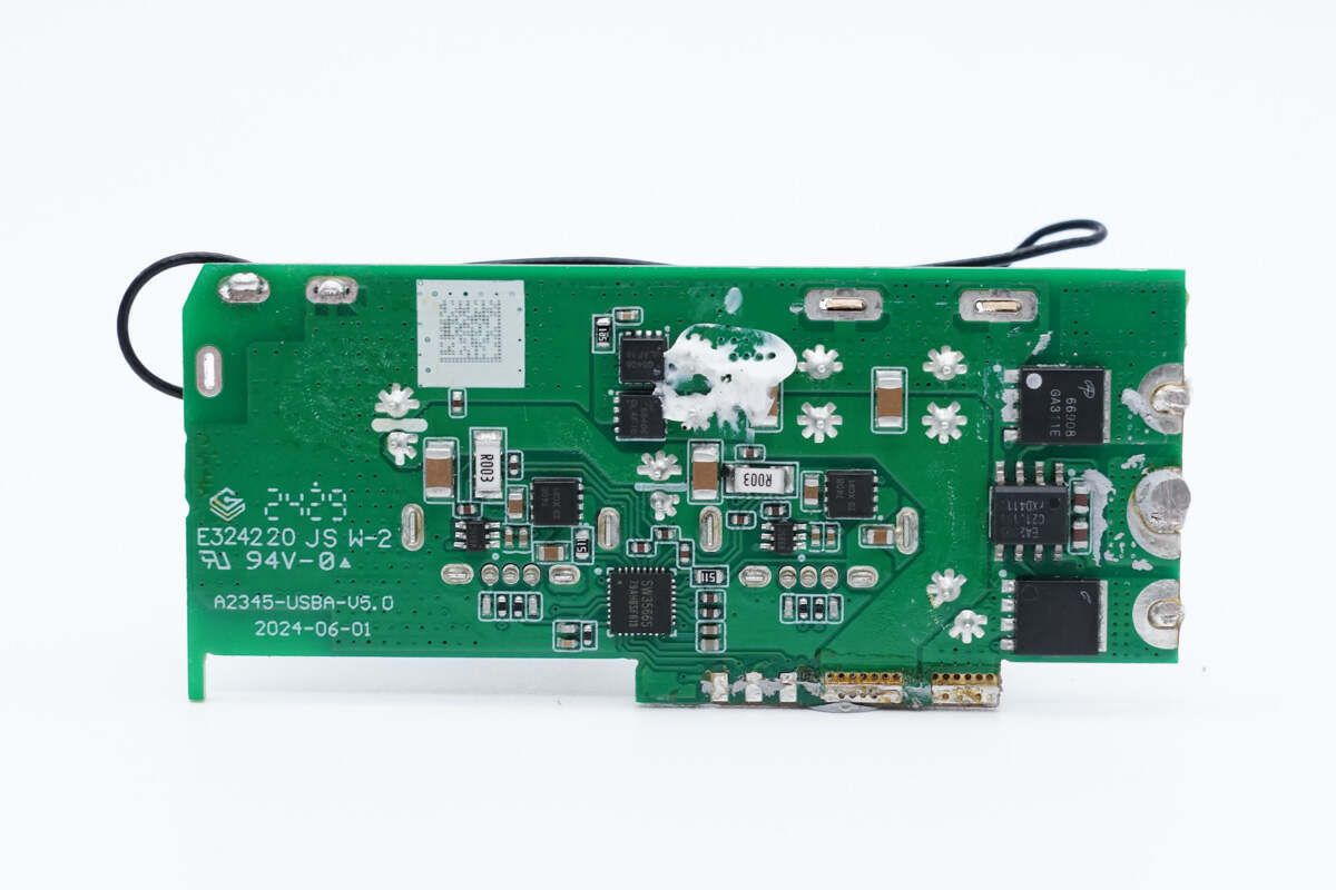
Remove the small PCB. On the back are the synchronous rectifier controller, synchronous rectifier, buck protocol chip, synchronous buck MOSFET, current detection chip, and output VBUS MOSFET.
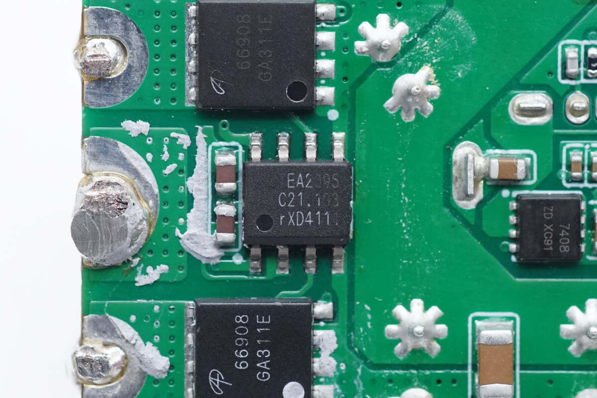
The synchronous rectifier controller is from NXP. It has two built-in drivers that can drive two synchronous rectifiers at the same time and support independent operation, making it suitable for LLC resonant power supply use. Model is TEA2095.
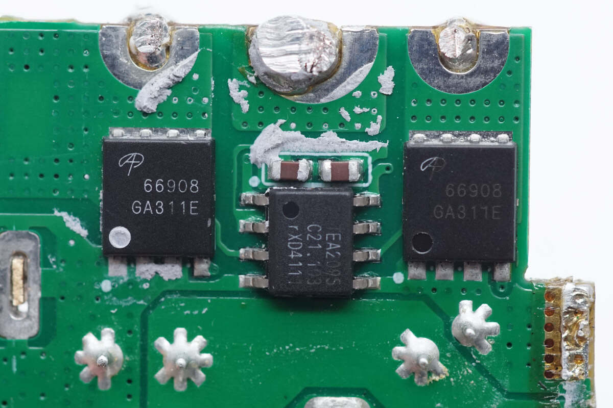
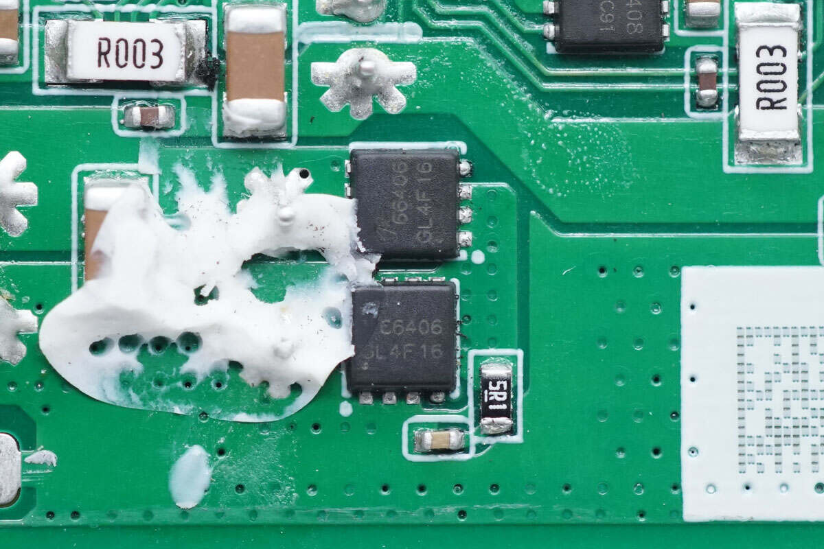
The two synchronous rectifiers are from AOS and adopt DFN5*6 package. 100V 4.2mΩ. Model is AONS66908.
There is the information about AOS AONS66908.
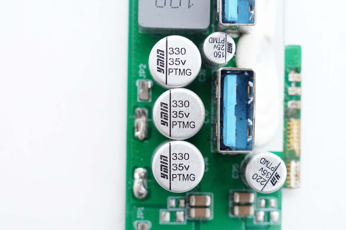
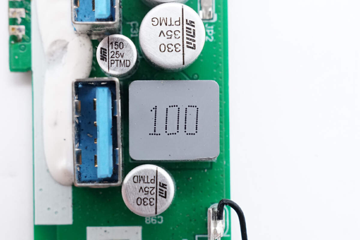
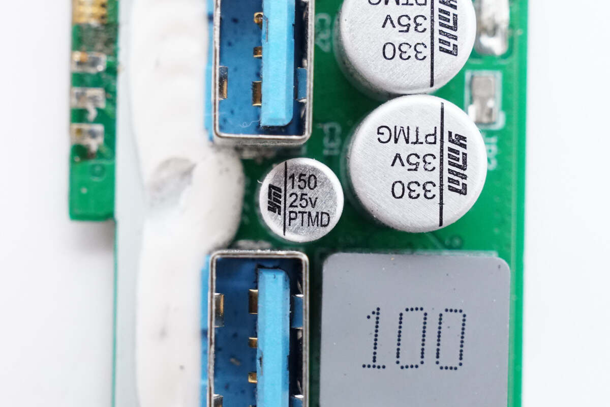
The three output solid capacitors are from YMIN. 35V 330μF.
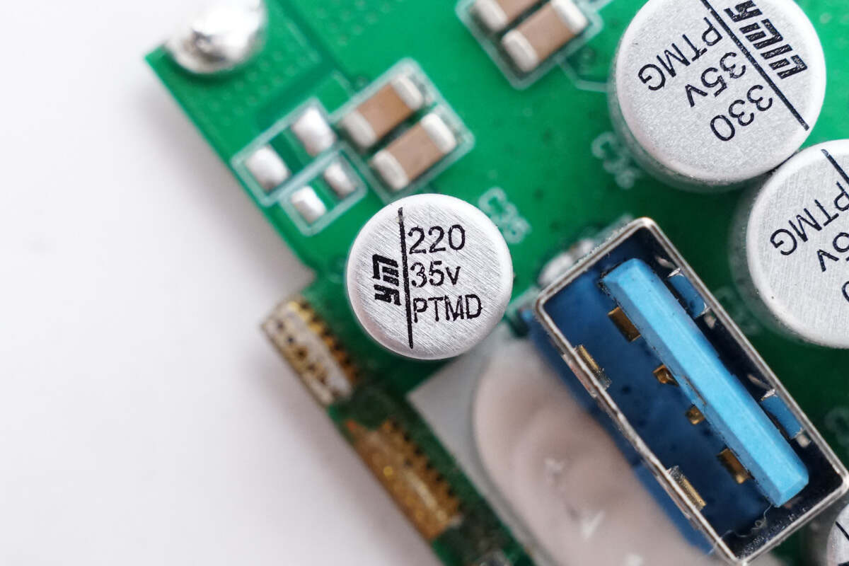
The fourth solid capacitor is also from YMIN. 35V 220μF.
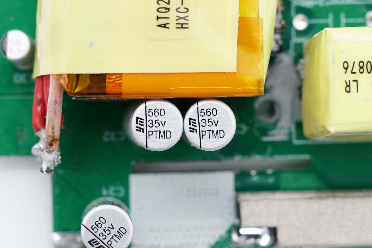
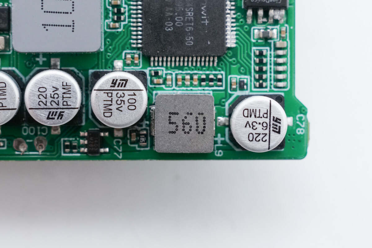
Two synchronous rectifier output solid capacitors are also from YMIN. 35V 560μF.
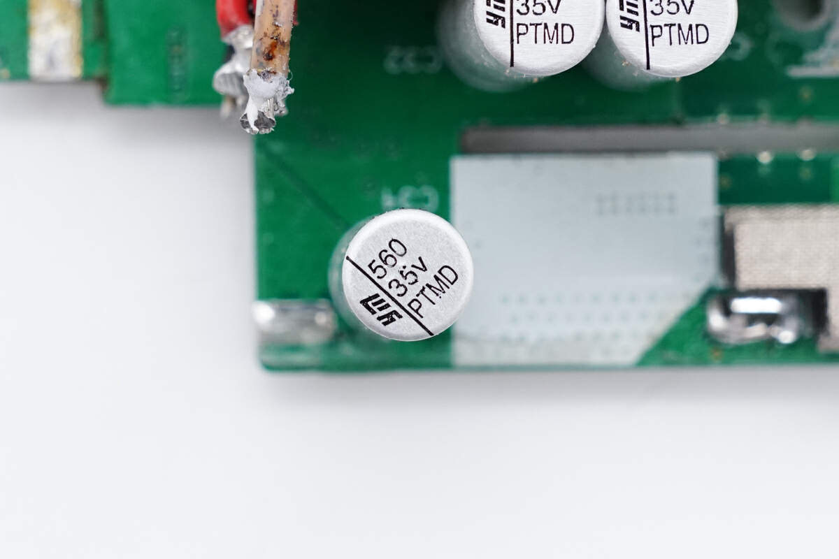
The third one is also from YMIN. 35V 560μF.
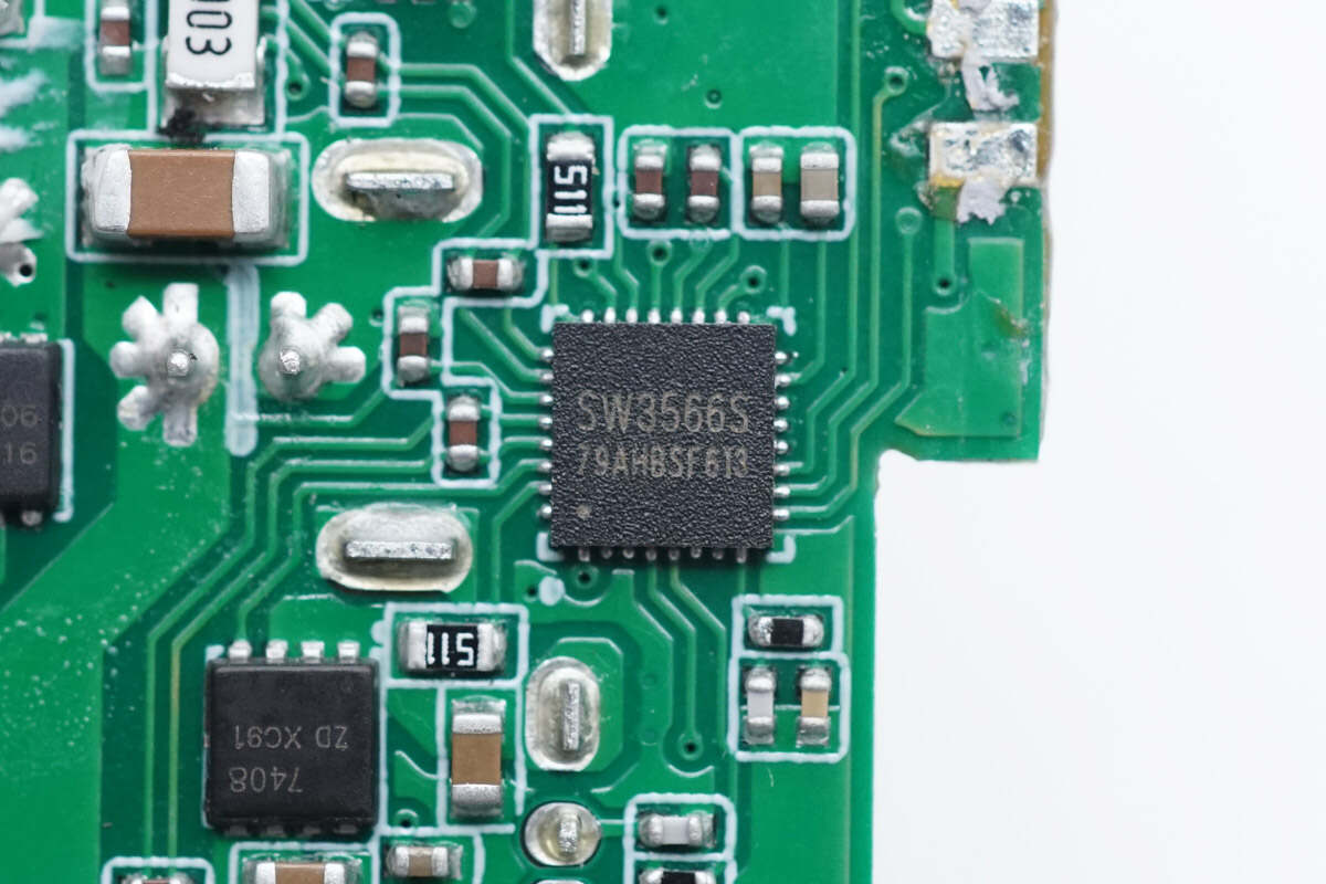
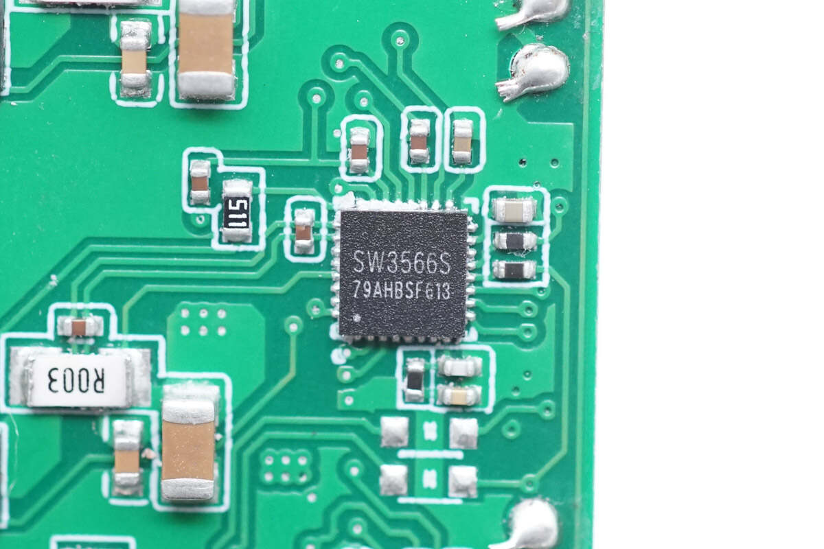
The buck controller of USB-A1 and USB-A2 is from iSmartWare. This is a dual-port SoC with an integrated 7A Buck controller, supporting 140W (28V@5A) power output and supporting multiple fast charging protocols such as PD3.1. Model is SW3566S.
It has a built-in ARM Cortex-M0 core, integrated Type-C interface logic, PD3.1 PHY, UFCS PHY, SCP/AFC PHY, TFCP PHY, and QC/PE/SFCP and other fast charging protocol detection circuits. Only a small number of peripheral devices are needed to form a complete high-performance dual-port fast charging solution.
It integrates CC/CV mode, dual-port management logic, and bus voltage detection and can achieve dual-port buck output with the corresponding buck switch tube and VBUS MOSFET. The chip's built-in buck converter has operating frequencies of 125KH, 180KH, 333KH, and 500KH and supports PWM and PFM working modes. Output current, line loss compensation, and other protection thresholds can be set through the MCU. The built-in ADC can realize data sampling of 9 channels, such as input and output voltage, output current, chip temperature, etc., and supports external MCU for parameter display.
It supports 36V input voltage, maximum output current 7A, built-in soft start, input overvoltage/under voltage protection, output overvoltage/under voltage protection, output overcurrent/short circuit protection, DP/DM/CC overvoltage protection, chip overtemperature protection, external NTC thermistor protection, as well as power limit protection. It adopts QFN4*4-32 package.

There is the information about iSmartWare SW3566S.
The two synchronous buck MOSFETs are from AOS and adopt DFN 3x3 EP package. 40V 6.1mΩ. Model is AONR66406.
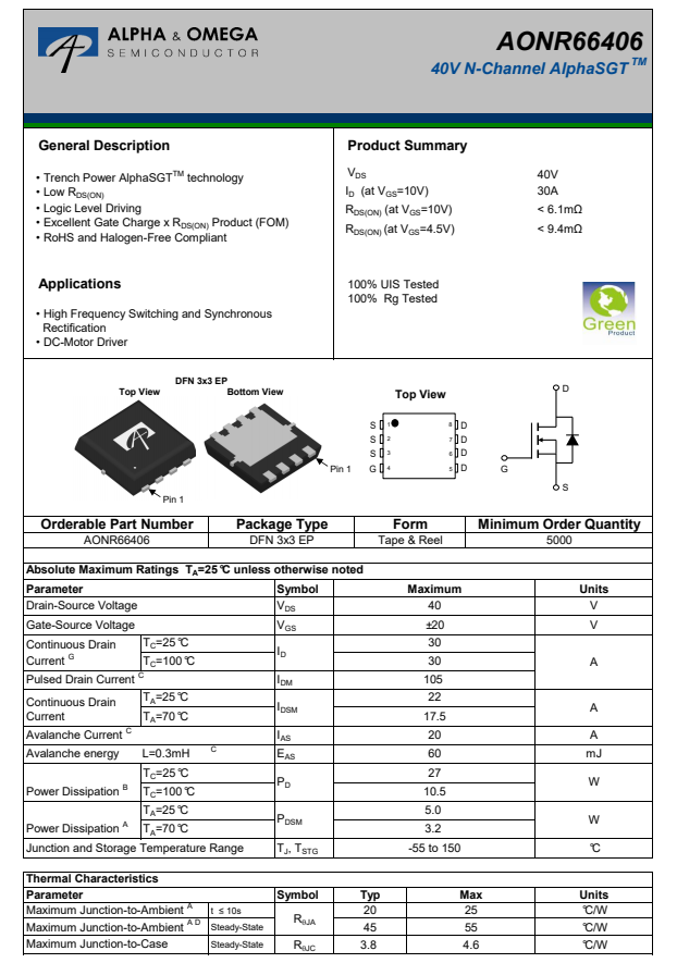
There is the information about AOS AONR66406.
There is the buck inductor.
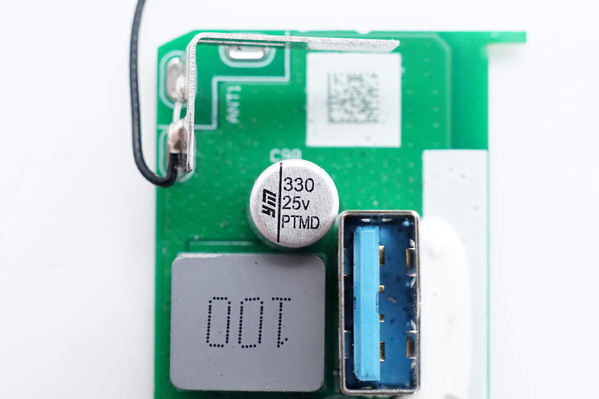
The buck output solid capacitor is from YMIN. 25V 330μF.
The specification of the other one is 25V 150μF.
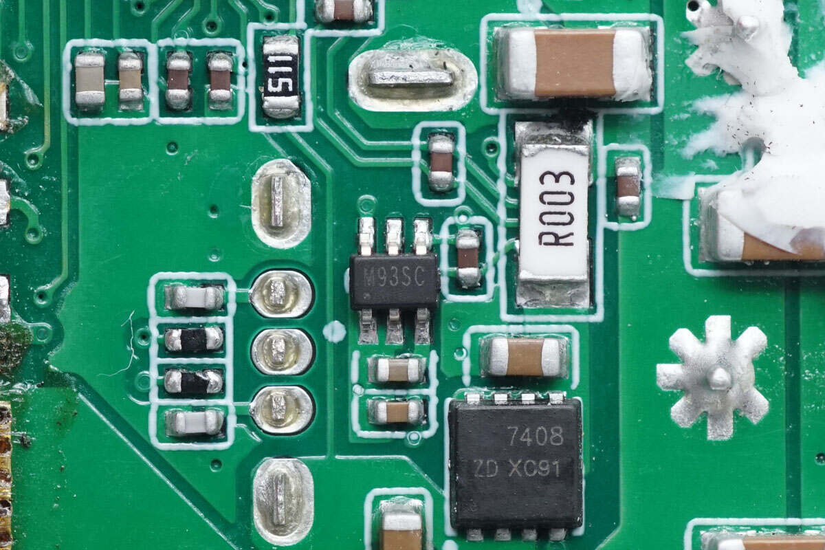
The current detection chip of the USB-A1 port adopts SC70-6 package is from SGMICRO and marked with M93. It supports high-side and low-side applications, supports bidirectional current detection, supports 28V supply voltage, and is used for USB-C port current detection. Model is SGM8199A2.
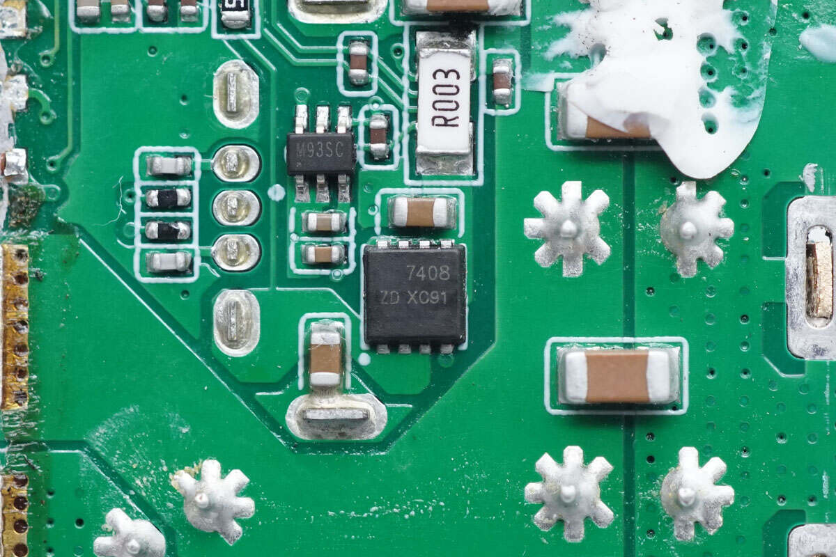
The USB-A1 port output VBUS MOSFET is marked with 7408.
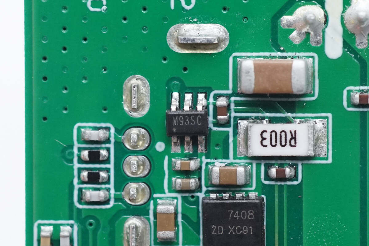
The current detection chip of USB-A2 port is also from SGMICRO. Model is SGM8199A2.
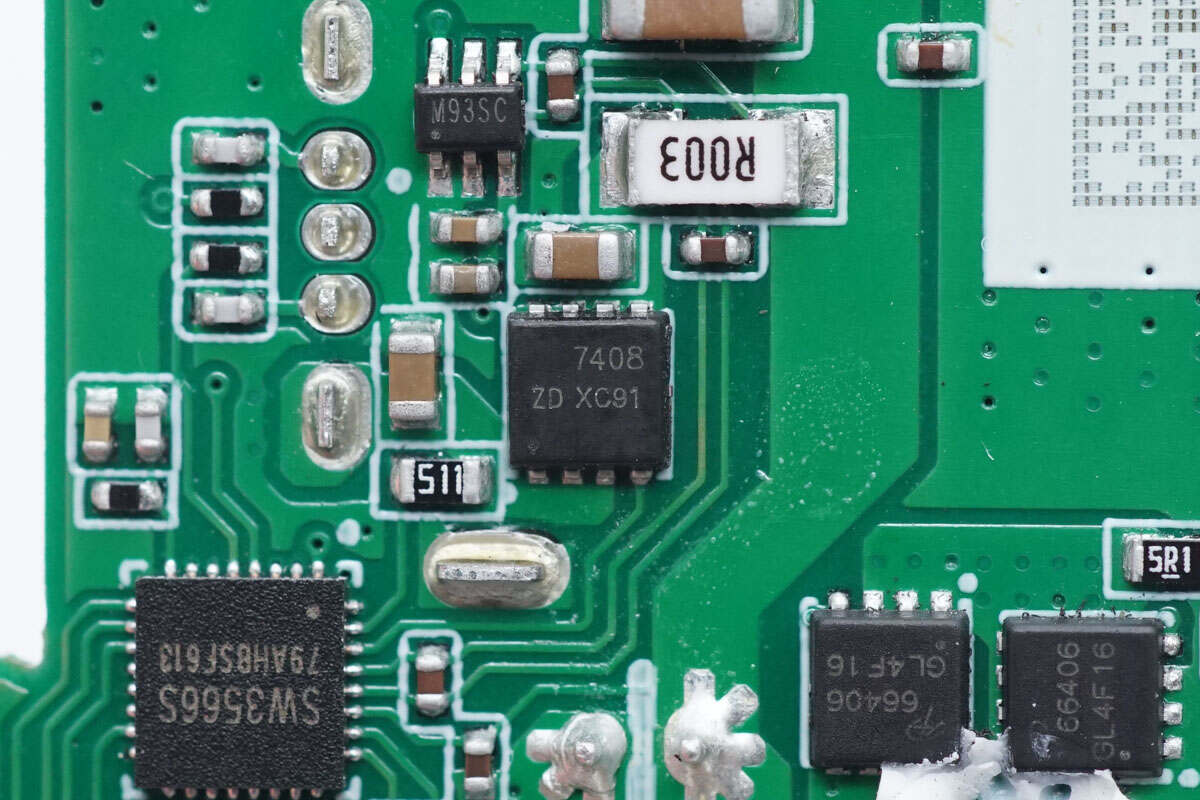
The output VBUS MOSFET is the same model as that of the USB-A1 port.
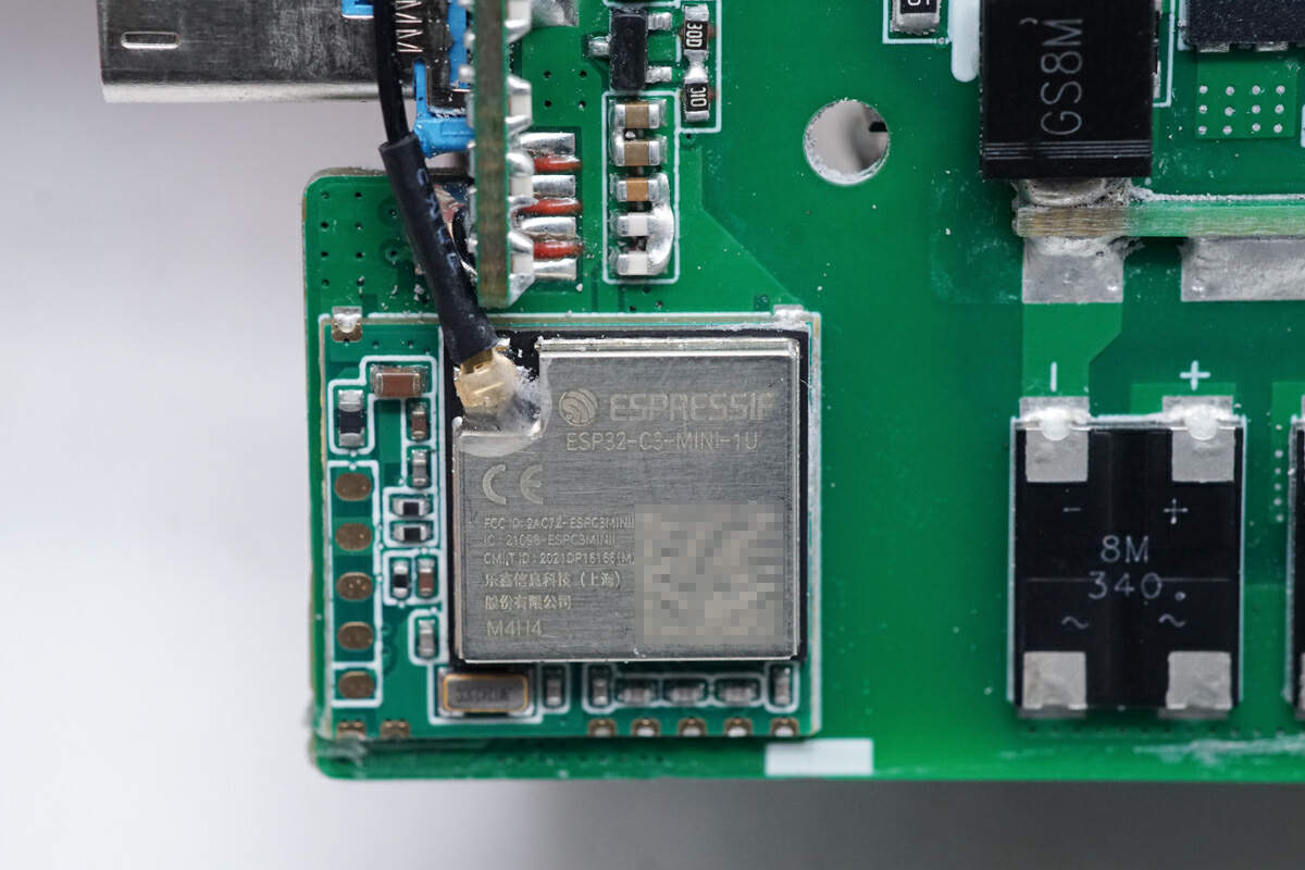
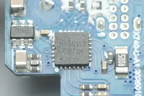
The wireless communication module is from ESPRESSIF. Model is ESP32-C3-MINI-1U.
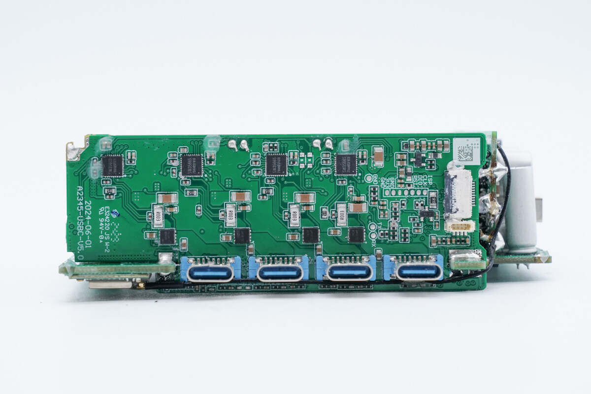
The output PCB has four buck protocol chips and four VBUS MOSFETs, which are used to control the output of four USB-C ports. There is also a connection slot for the TFT color screen and knob module on the right.
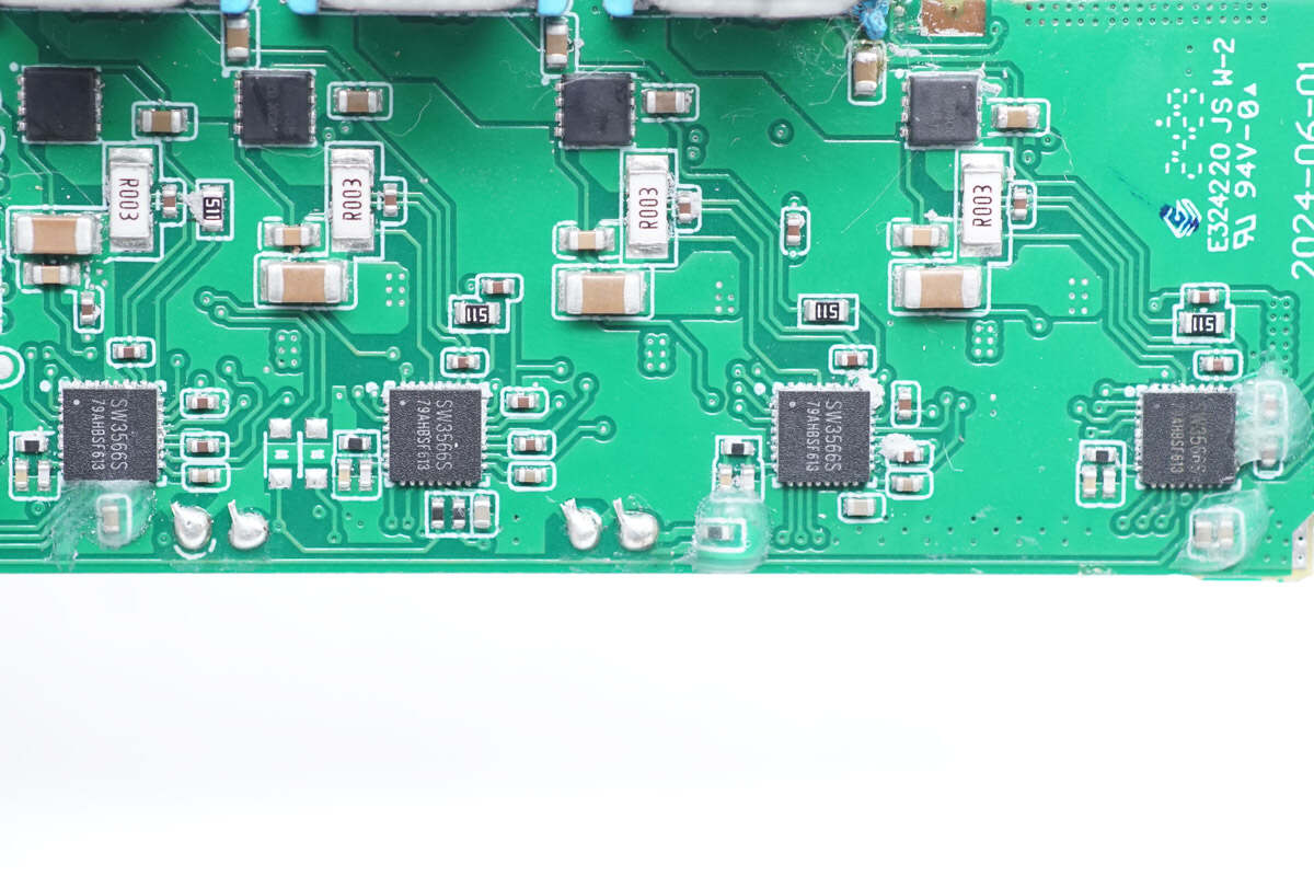
The four buck protocol chips are all from iSmartWare and have the same model.
The buck protocol chips for the four USB-C ports all come from iSmartWare. This new flagship chip integrates a synchronous buck controller, a protocol chip, and an MCU into one chip, thus simplifying the circuit structure. It supports up to 28V5A 140W fast charging and has passed PD3.1 and UFCS certifications. Model is SW3566.
There is the information about iSmartWare SW3566.
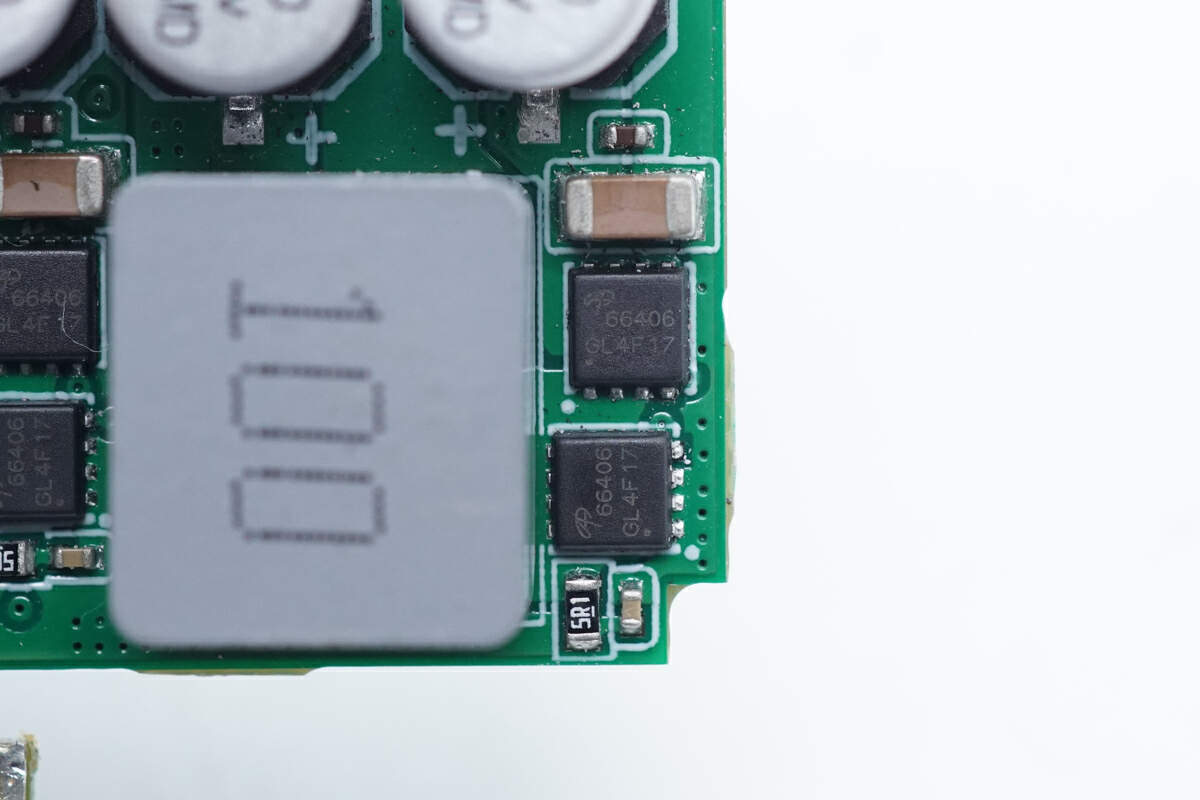
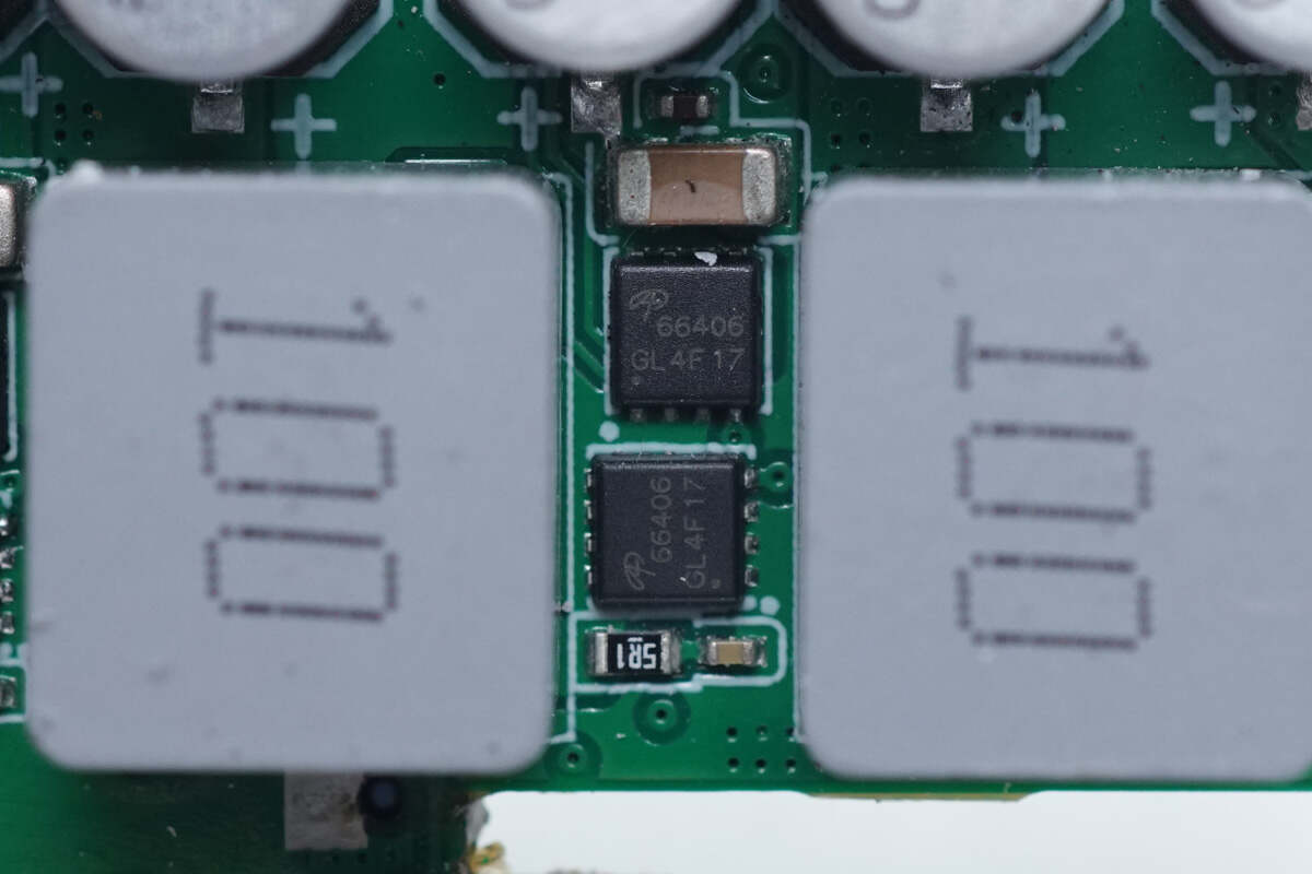
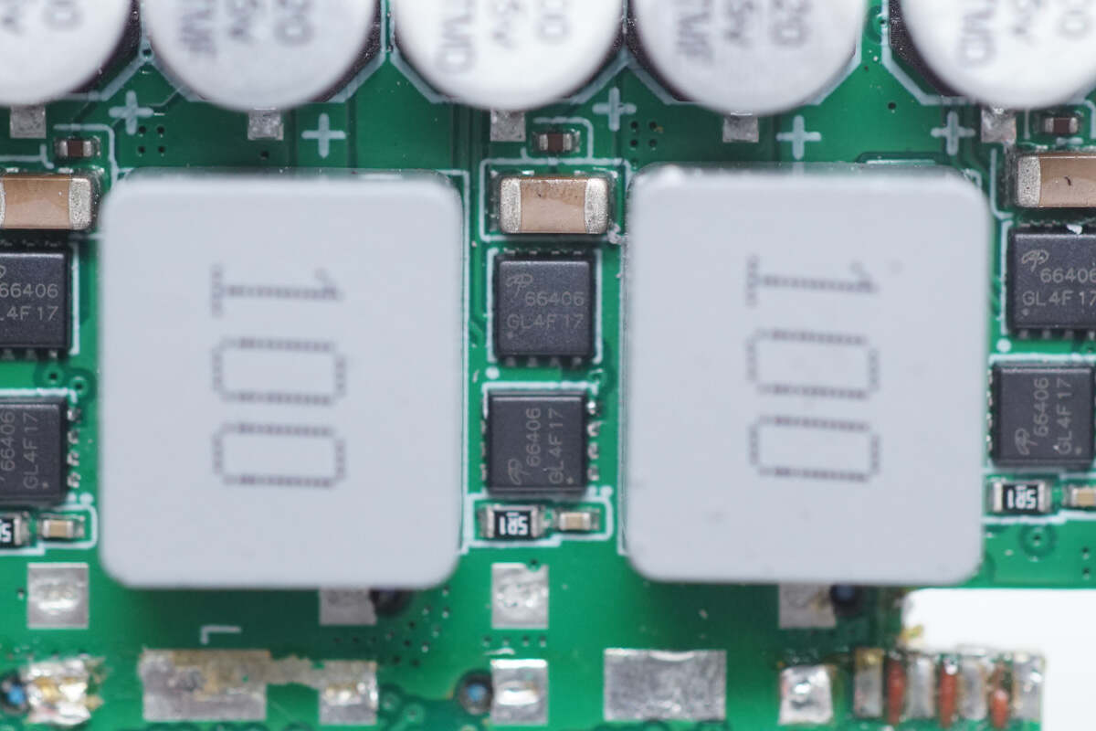
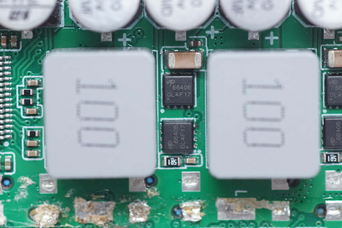
The four sets of synchronous buck MOSFETs are from AOS. Model is AONR66406.
This is the second set of synchronous buck MOSFETs.
This is the third set.
This is the fourth set.
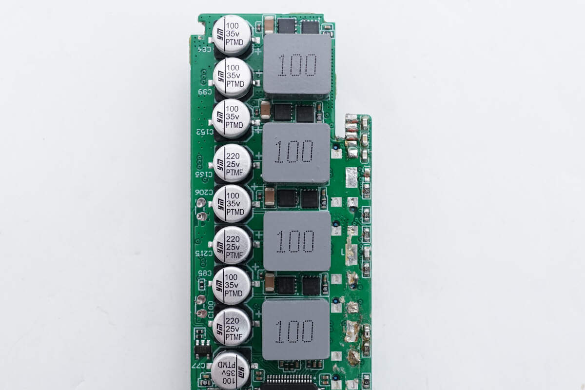
These are four buck inductors.
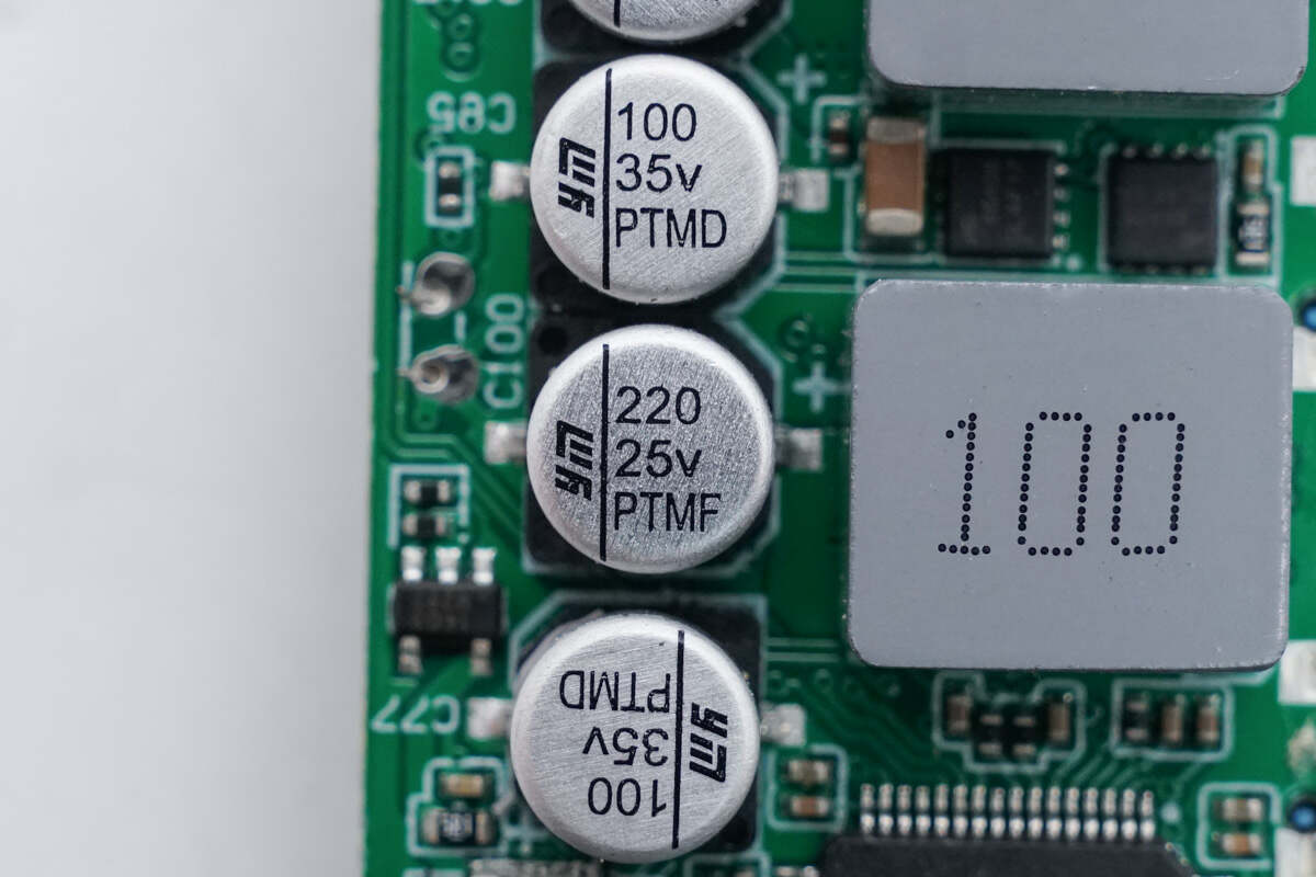
The nine solid capacitors used for the four-circuit buck output filtering are all from YMIN. The specifications are 35V 100μF and 25V 220μF, respectively.
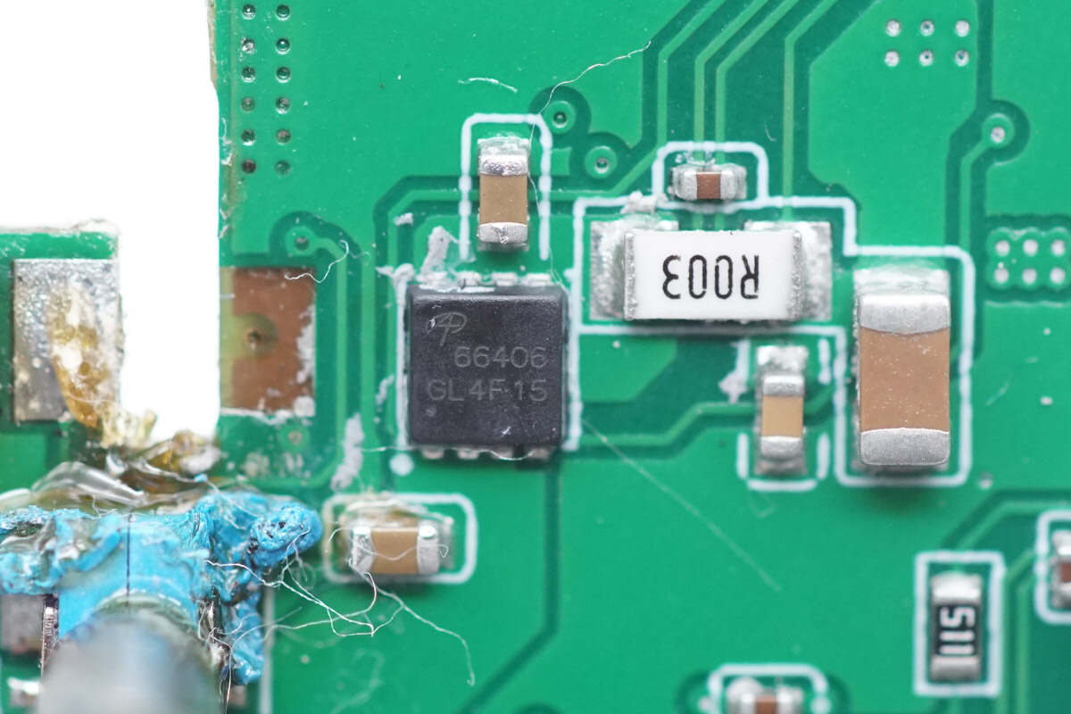
The output VBUS MOSFET of the USB-C1 port is from AOS. Model is AONR66406.
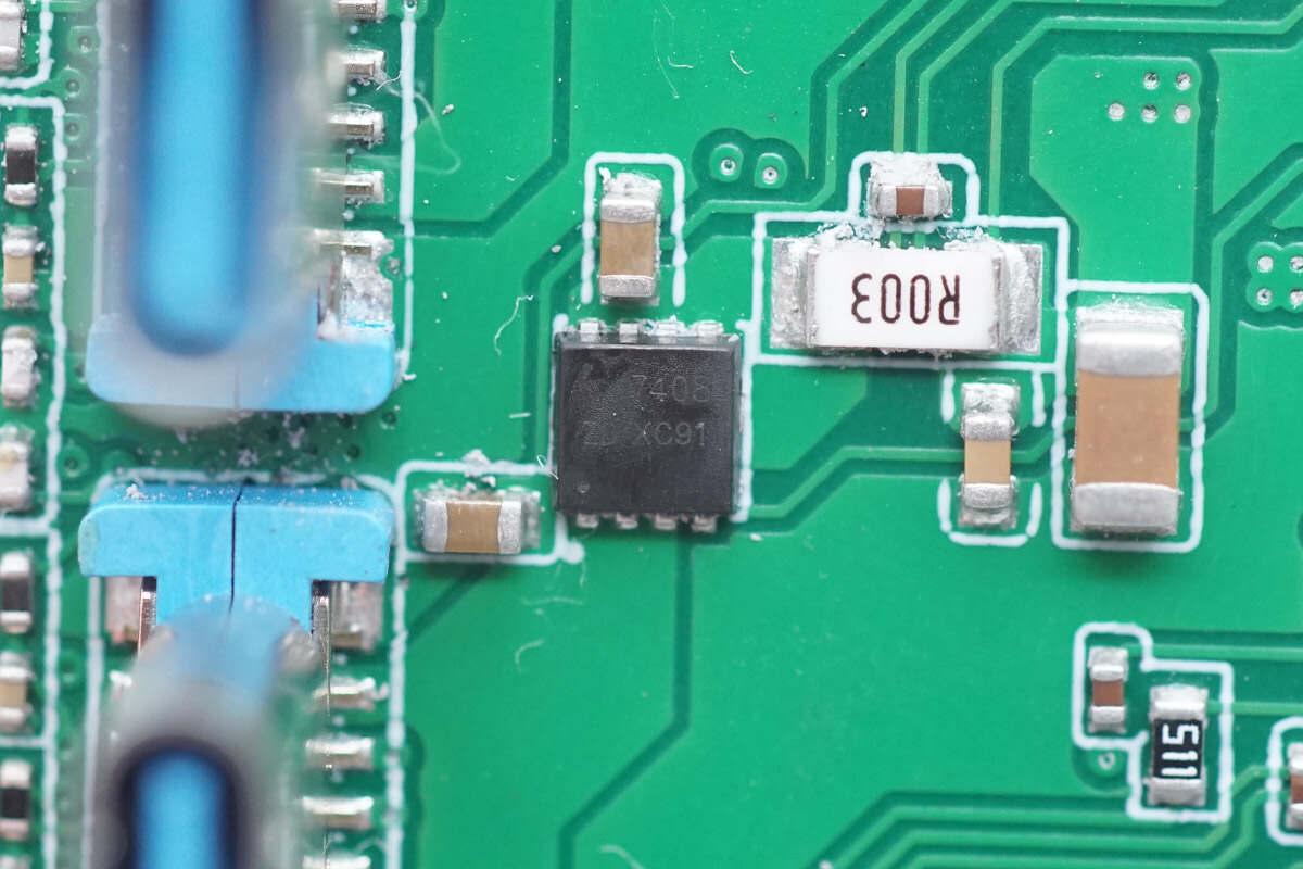
The output VBUS MOSFET of the USB-C2 port is marked with 7408.
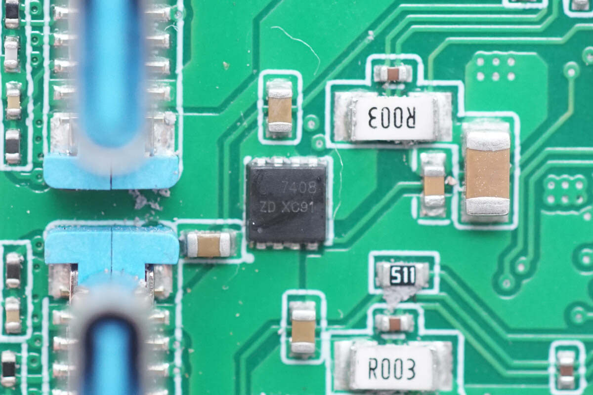
The output VBUS MOSFET of the USB-C3 port is the same as that of the USB-C2 port.
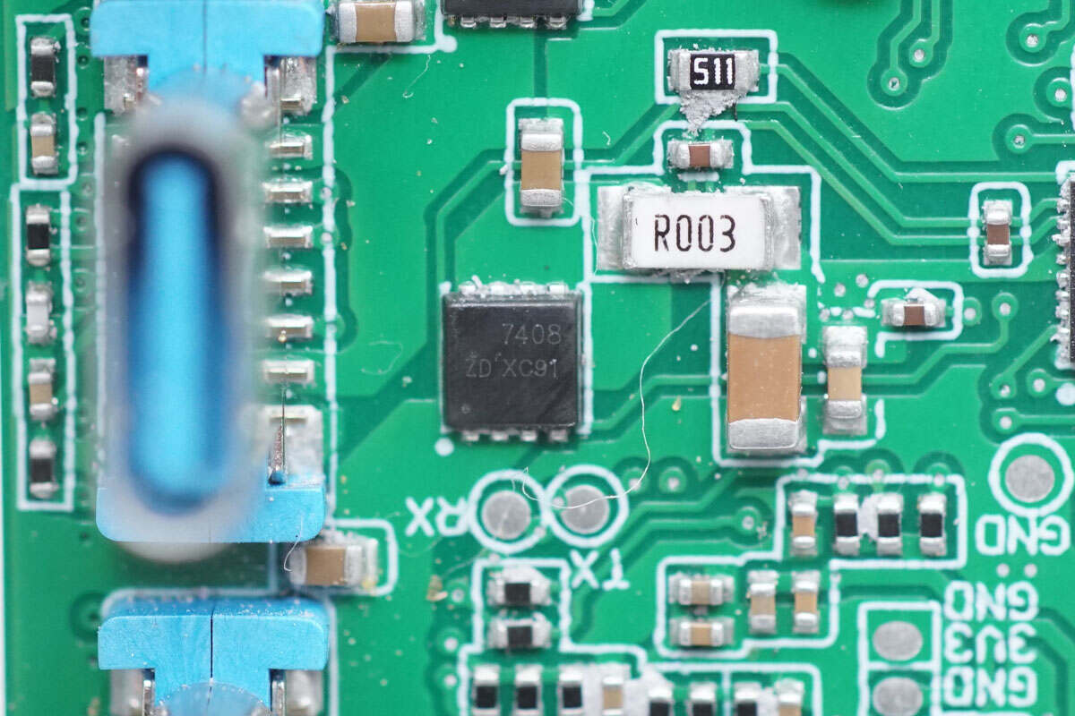
The output VBUS MOSFET of the USB-C4 port is the same as that of the USB-C2 and USB-C3 ports.
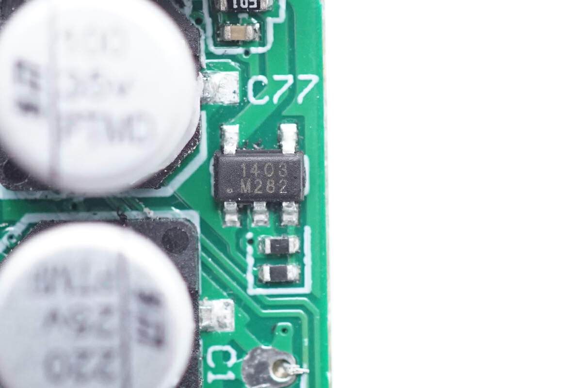
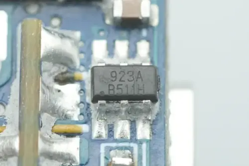
The synchronous buck converter is from KIWI and marked with 1403. It is capable of driving load currents up to 1A. It supports a wide voltage input of 6-40V and is suitable for power regulation of unregulated power supplies in the industrial field. Model is KP521403.
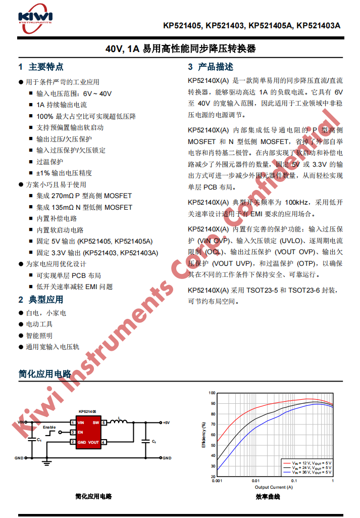
There is the information about KIWI KP521403.
This is the alloy buck inductor.
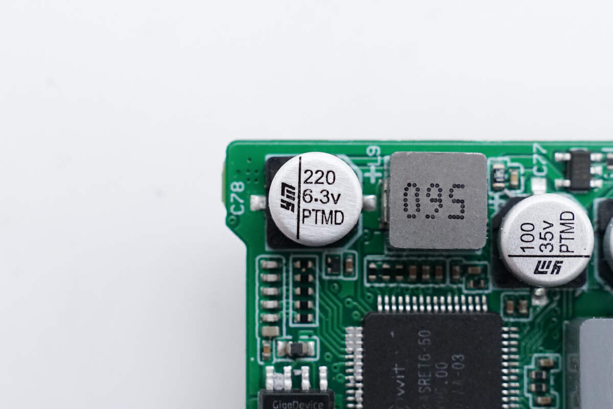
The buck output solid capacitor is from YMIN. 6.3V 220μF.
The other solid capacitor is 6.3V 100μF.
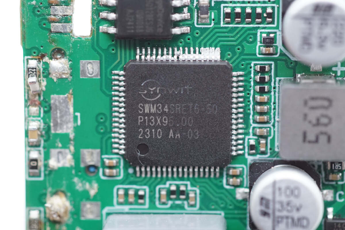
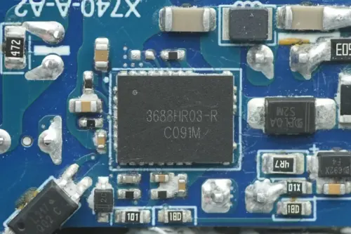
The MCU used for screen display driving and control is from Synwit. It is a 32-bit microcontroller based on ARM® Cortex®-M33. It has outstanding features such as high performance, low power consumption, and high code density. Model is SWM34SRET6-50.
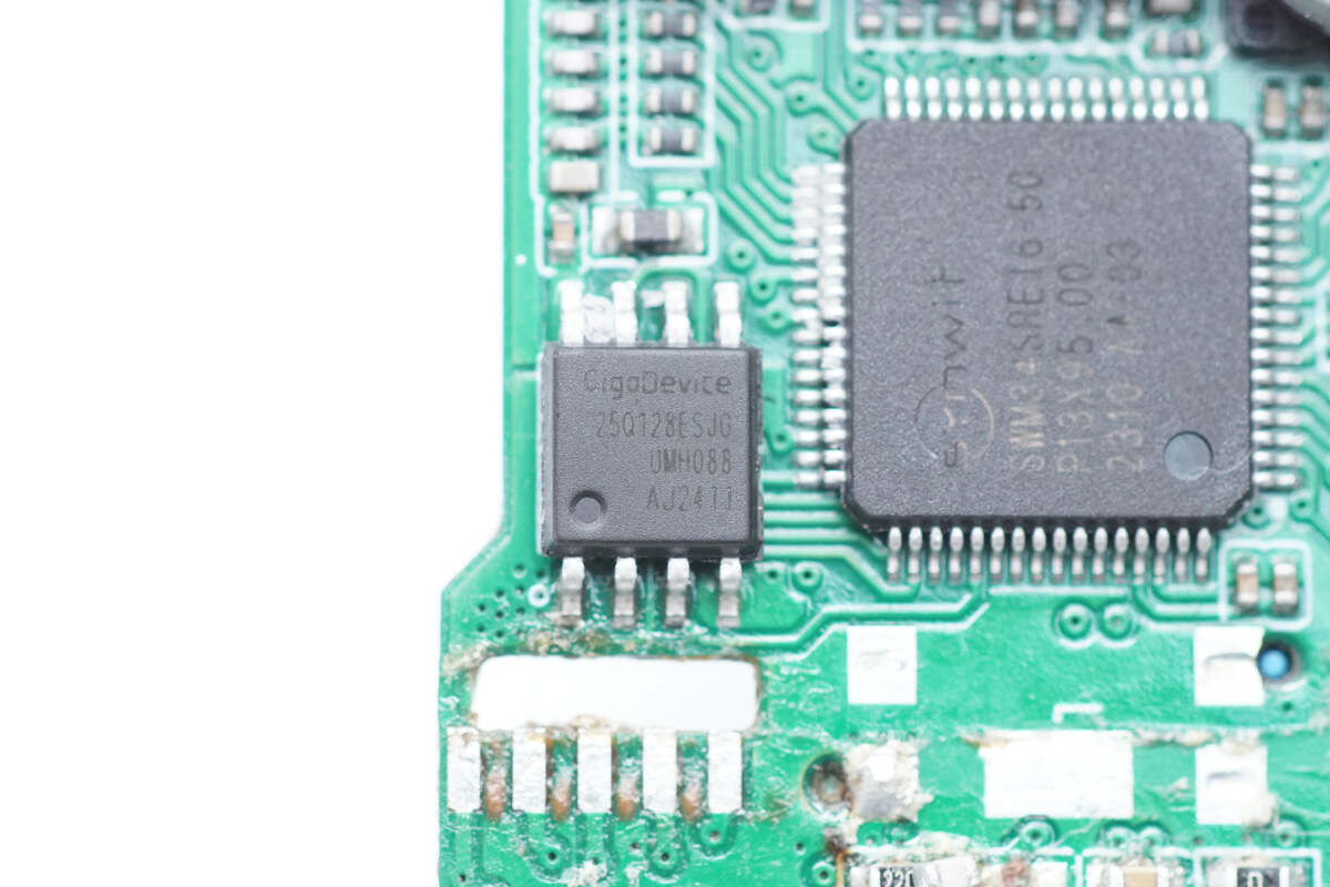
The memory is from GigaDevice. Model is GD25Q128E.
These are two thermistors used to detect the internal temperature of the charger.
Well, those are all components of the ANKER Prime 250W GaN Charger.
Summary of ChargerLAB
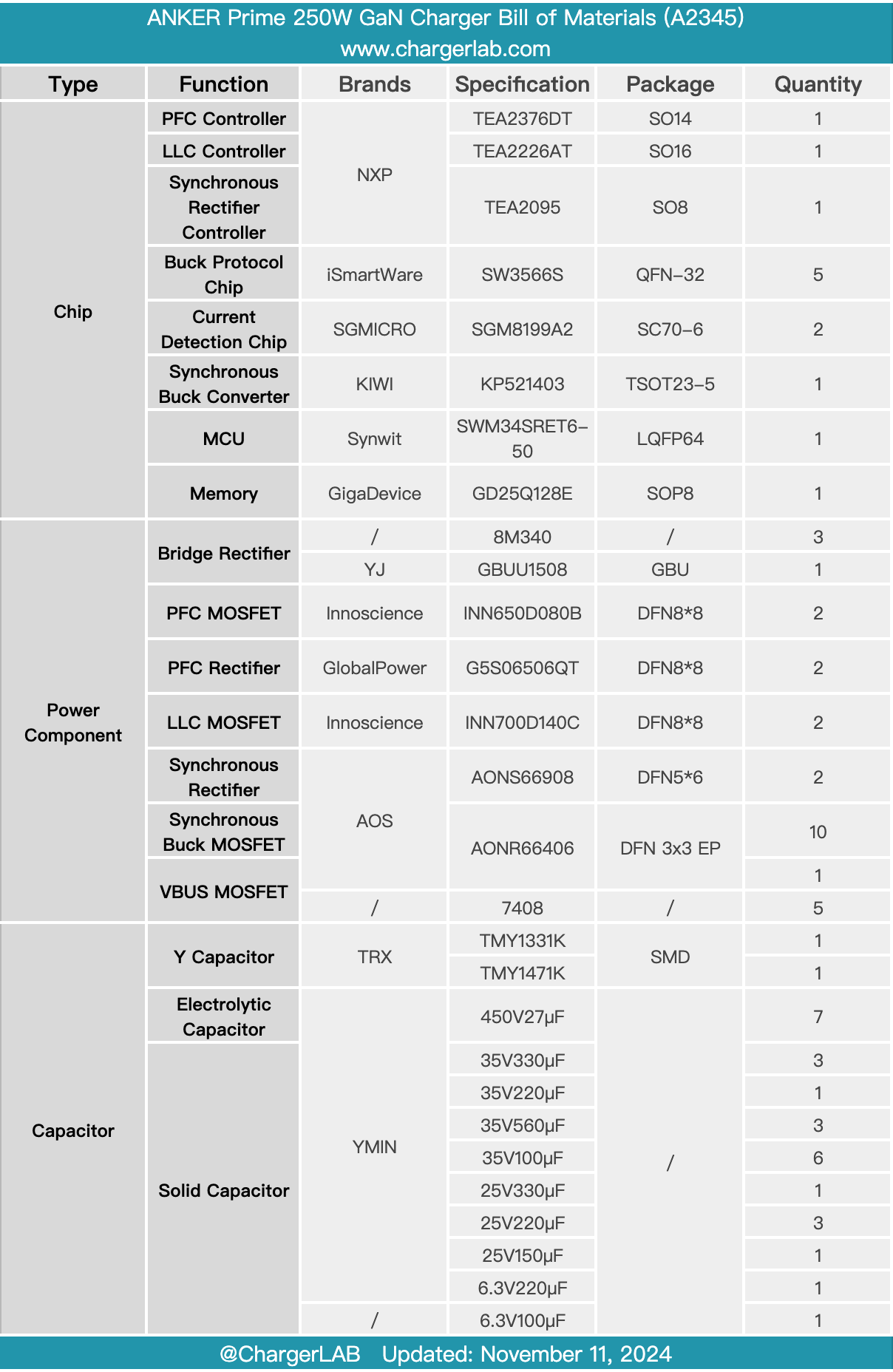
Here is the component list of the ANKER Prime 250W GaN Charger for your convenience.
It adopts a silver shell with a black panel, which looks simple and stylish. It is equipped with four USB-C ports and two USB-A ports. Thanks to the use of five iSmartWare protocol buck chips, it not only has good compatibility but also supports charging protocols such as PD3.1 140W, 55W PPS, Huawei 22.5W SCP, and UFCS, with a total output power of 250W. It can meet the needs of fast charging of laptops, tablets, phones, headphones, and other devices at the same time, and its performance is powerful.
After taking it apart, we found it adopts PFC+LLC architecture. The NXP TEA2376DT+TEA2226AT+TEA2095 full solution is used, and Innoscience GaN devices and GlobalPower silicon carbide devices are also used. It adopts a five-circuit independent buck circuit design, and each circuit adopts iSmartWare SW3566S. The high integration and high-performance help simplify the product design and bring excellent performance. The PCBA module is filled with a large amount of potting compound and covered with a large area of heat sink. The shell is also covered with a thermal paste composed of copper foil and graphite. The screen is protected by sponge. The overall workmanship and materials are very good.
Related Articles:
1. Teardown of Anker Prime Charger (200W, 6 Ports, GaN)(A2683)
2. Teardown of Anker Prime 200W 6 Ports GaN Charger
3. Trump Same Style | Teardown of Anker MagGo Magnetic Power Bank (A1654)