Introduction
We have obtained the Anker Prime Charger (160W, 3 Ports, Smart Display). All three of its USB-C ports support 140W PD 3.1, with the ability to deliver a sustained 140W output on a single port for 24 hours without throttling. In multi-port use, the charger provides a maximum total output of 160W. Leveraging GaN technology and a highly refined stacked internal design, Anker has reduced the overall size to roughly that of an AirPods Pro charging case.
The charger is also equipped with a 1.3-inch color smart display that shows total output power, per-port power distribution, temperature, and other real-time data. It features a 360° gravity-based auto-rotation function for adaptive viewing angles. In addition, it supports Bluetooth connectivity for app-based control as well as continuous OTA updates. Next, we will take a closer look at the detailed design of this product.
Product Appearance
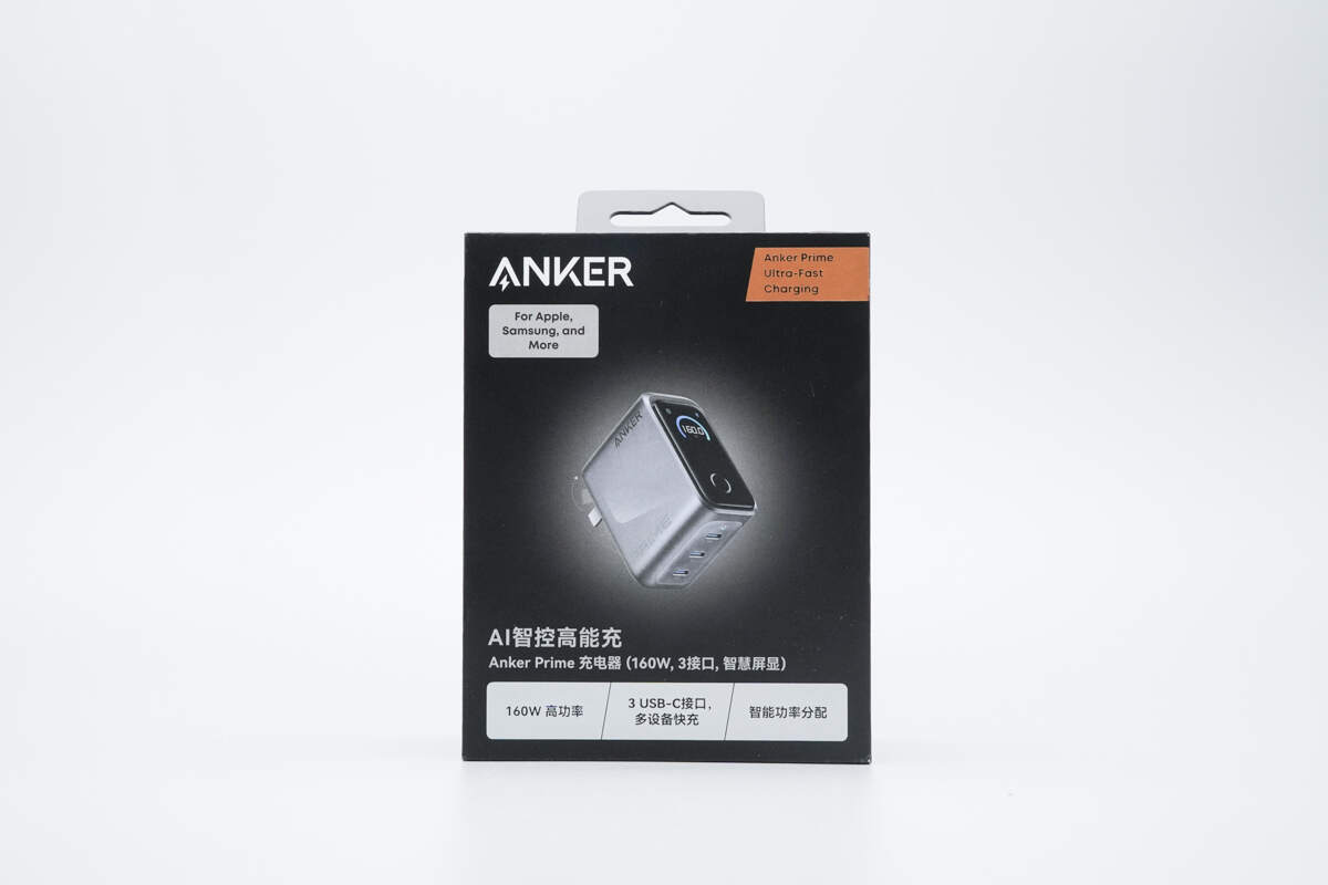
The front of the packaging features the ANKER branding, a product image, the product name, and key selling points.
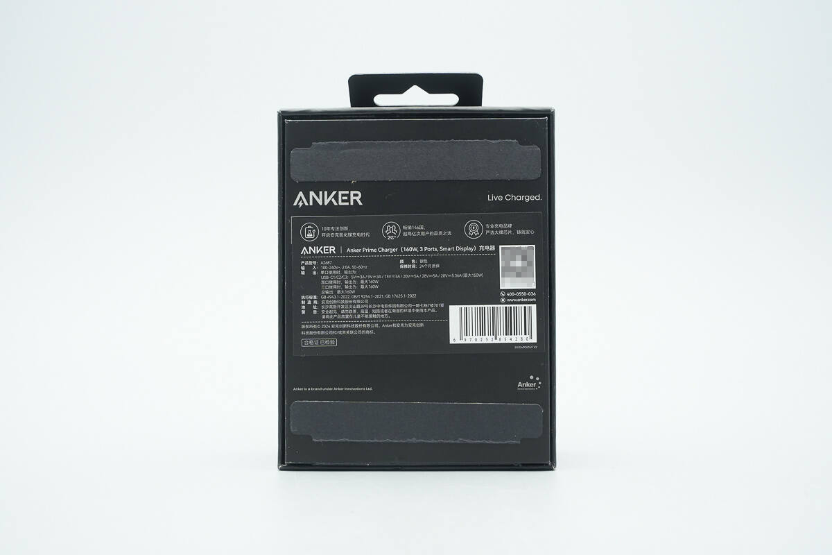
An information label is affixed to the back of the packaging.
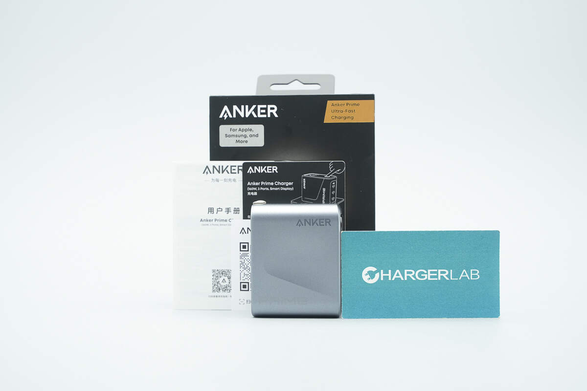
Inside the package are the charger and documentation, such as the user manual.
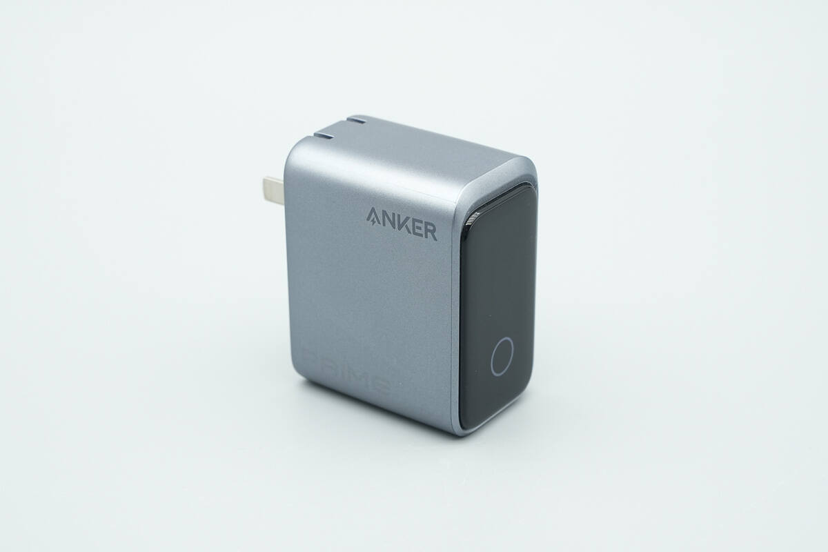
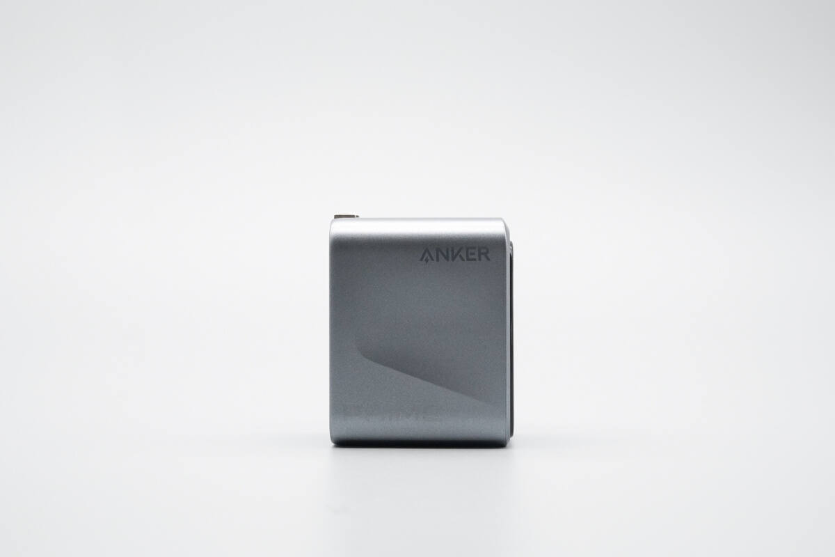
The main body is finished in a silver-gray metallic coating, while the top features a black glossy decorative panel.
The front is printed with the ANKER and PRIME branding.
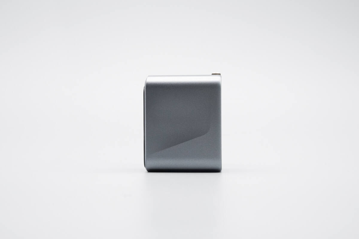
Both sides feature contoured side grooves, serving as decorative elements and enhancing the plug-in and unplugging experience.
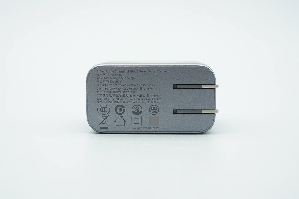
The input-side casing is printed with the technical specifications.
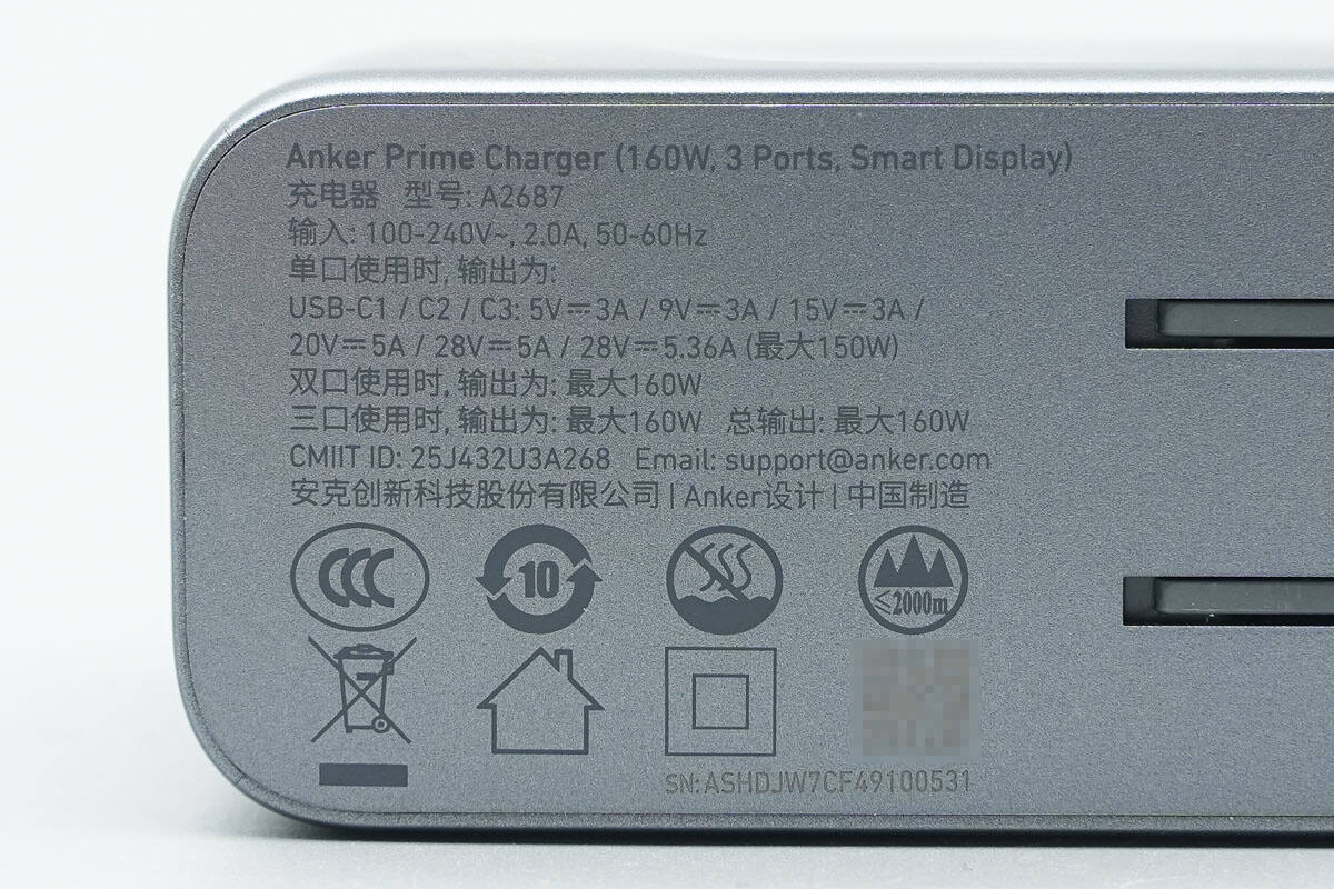
Model: A2687
Input: 100-240V~50/60Hz 2A
Output:
USB-C1/C2/C3: 5V 3A, 9V 3A, 15V 3A, 20V 5A, 28V 5A, 28V 5.36A (150W Max)
Dual-port output: 160W Max
Three-port output: 160W Max
Total output: 160W Max
The charger has passed PSE certification and Level VI energy efficiency certification.
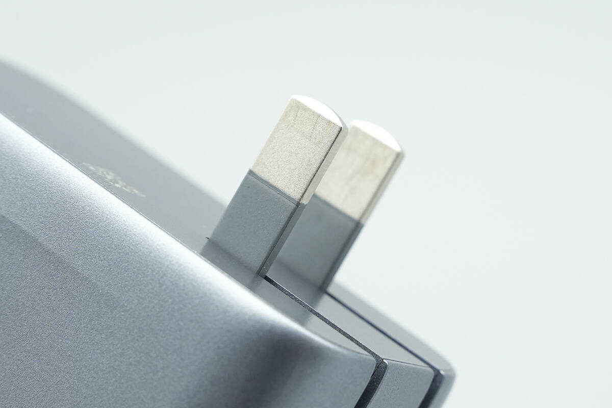
It is equipped with foldable prongs.
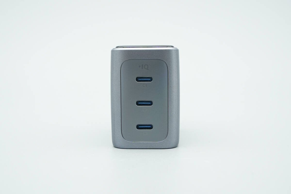
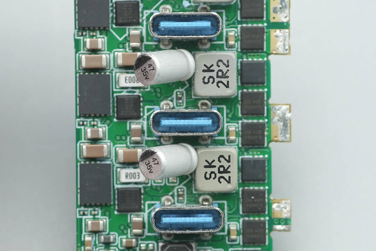
It is equipped with three USB-C ports, each labeled with its corresponding designation.
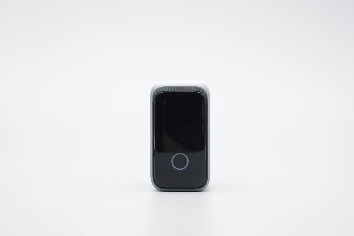
The top features a black decorative panel, housing a smart display and a touch-sensitive button.
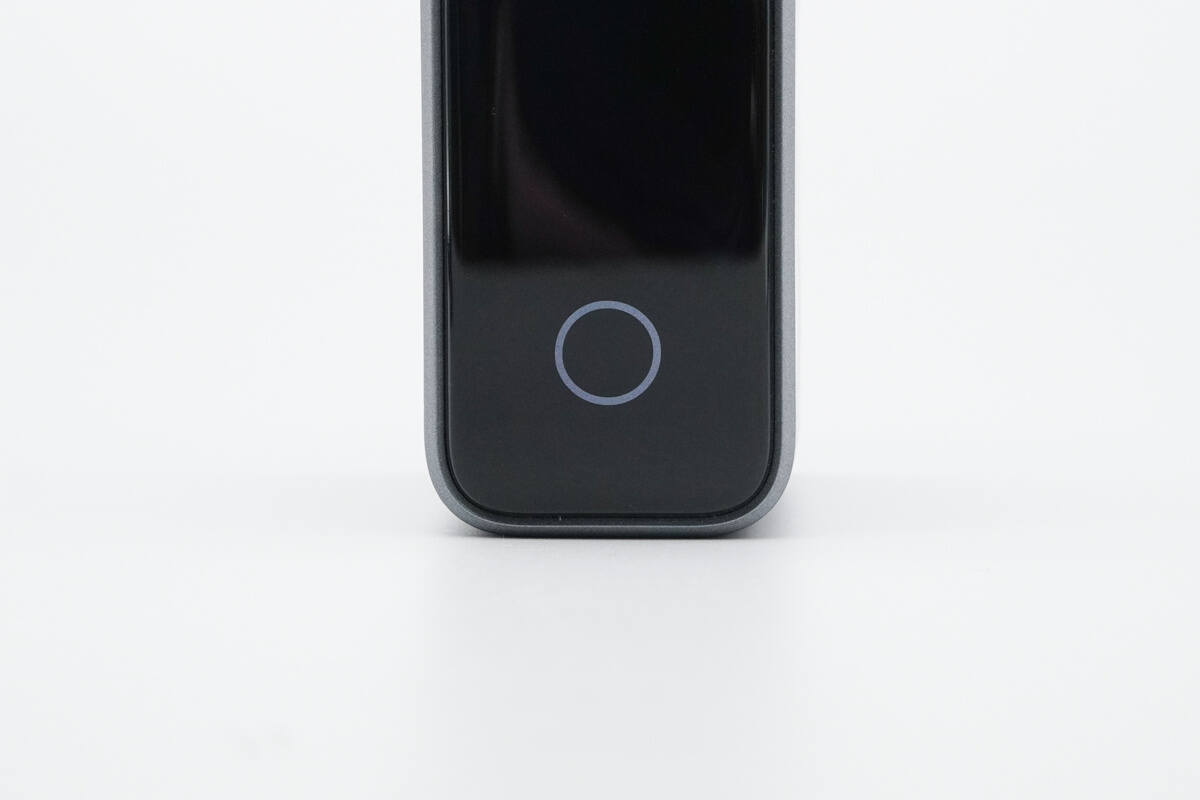
The touch-sensitive button is surrounded by an indicator ring.
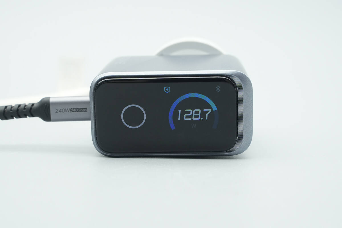
The display can show total output power, per-port power, charging mode selection, temperature, cable specifications, Bluetooth connection, and other information. It can be rotated via gravity sensing or by pressing the touch-sensitive button for a long time.
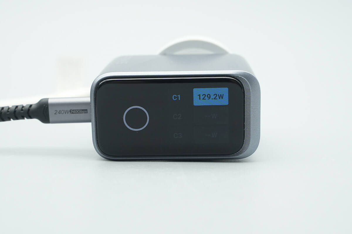
Overview of the per-port power display interface.
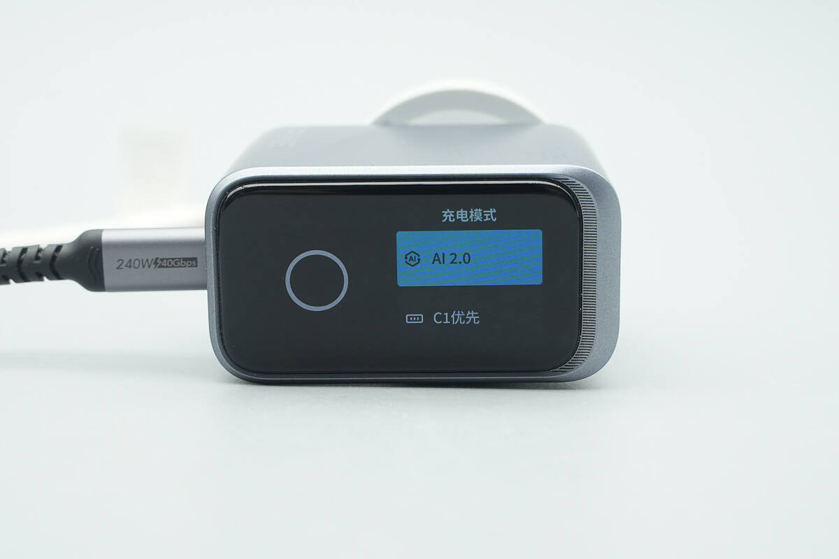
Overview of the charging mode selection interface, supporting seamless switching between AI Mode 2.0 and Standard Mode (with priority given to the C1 port).
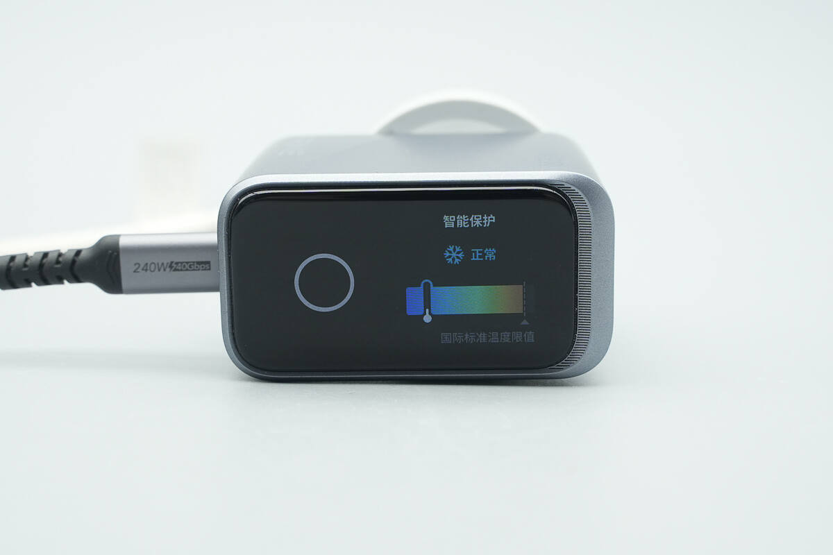
Overview of the temperature protection interface, which allows real-time temperature monitoring.
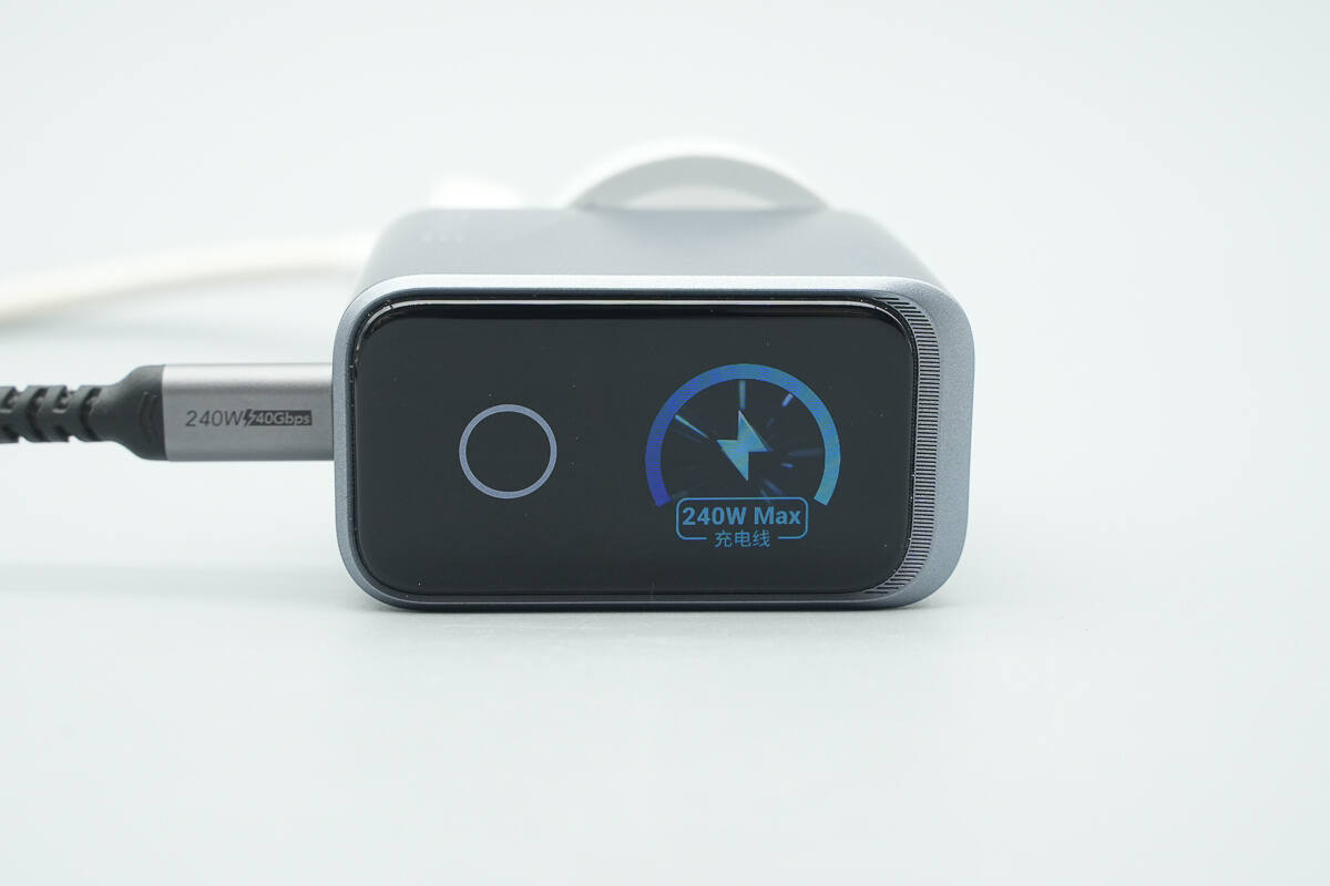
It can also read the specifications of the connected data cable.
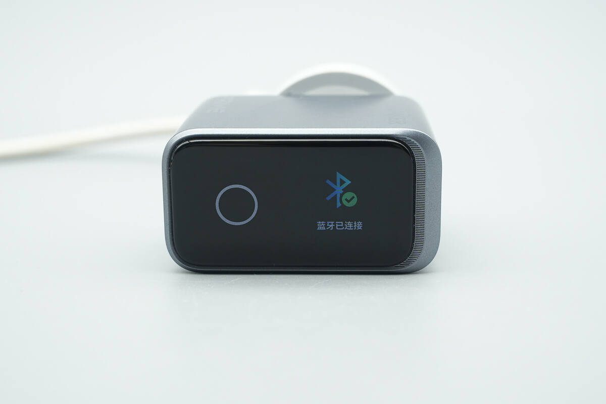
Overview of the Bluetooth interface. By connecting via Bluetooth to the app, users can view more detailed charging information and customize charging modes directly from their smartphone.
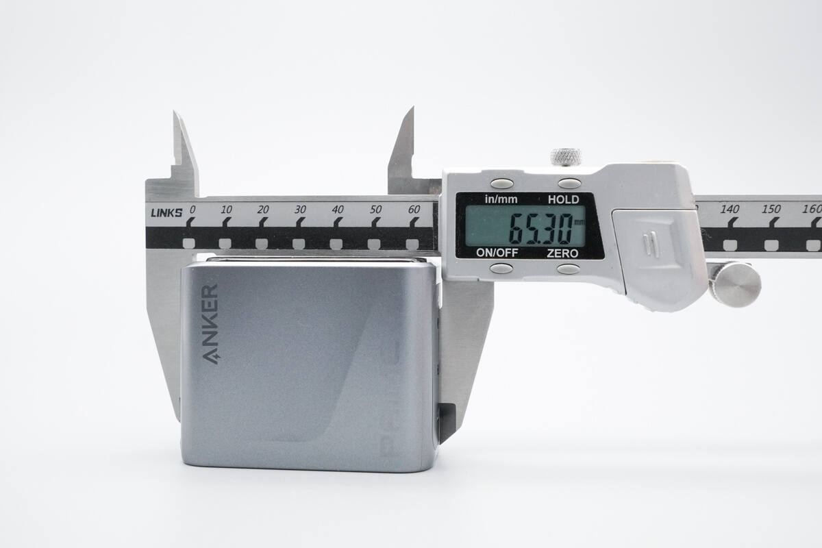
The length of the charger is about 65.3 mm (2.57 inches).
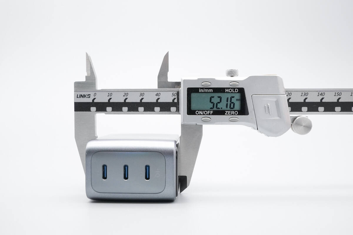
The width is about 52.16 mm (2.054 inches).
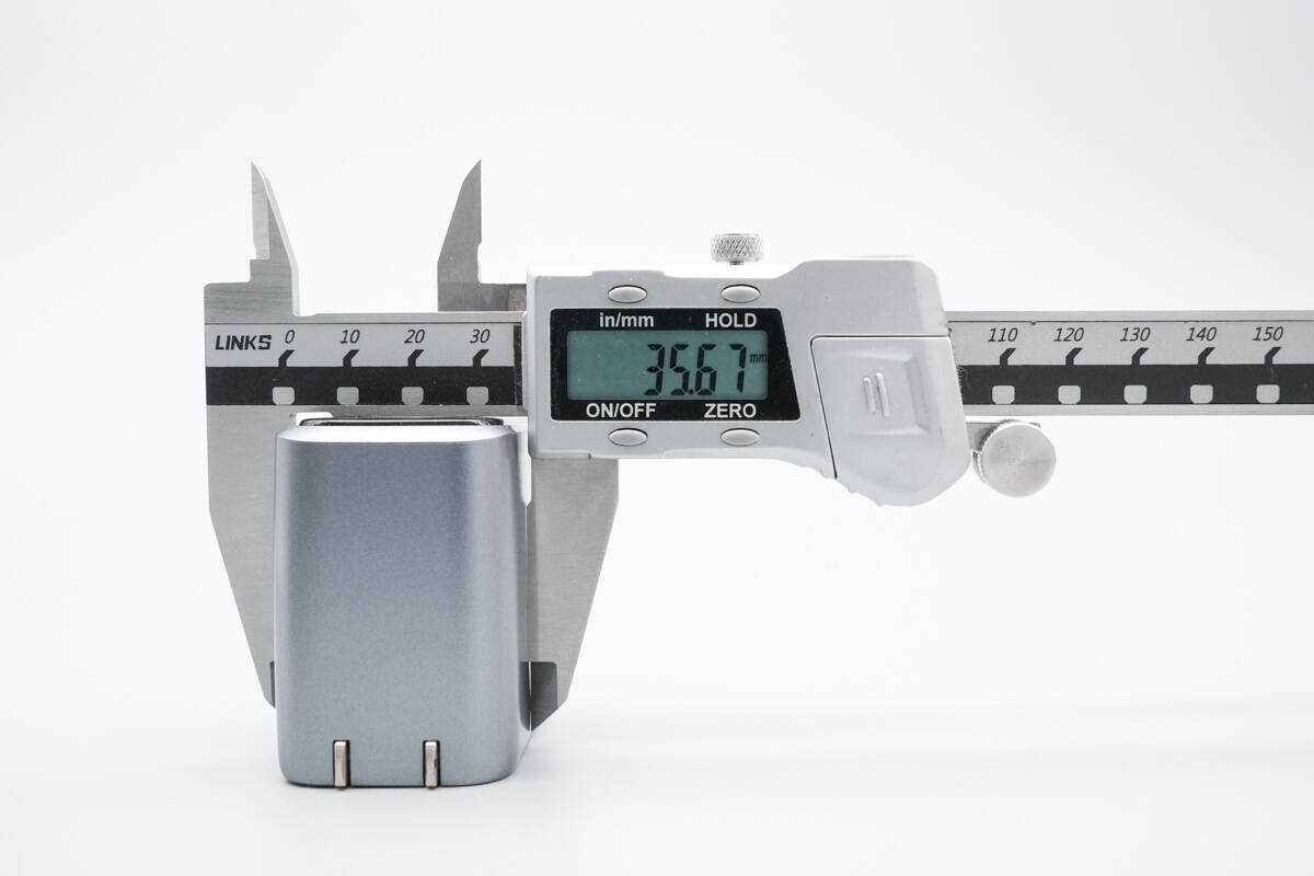
The thickness is about 35.67 mm (1.4 inches).
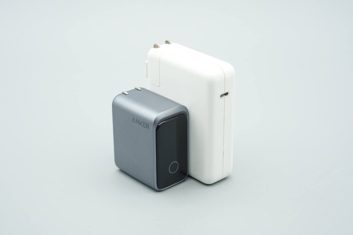
Compared with the Apple 140W charger, its size advantage is obvious.
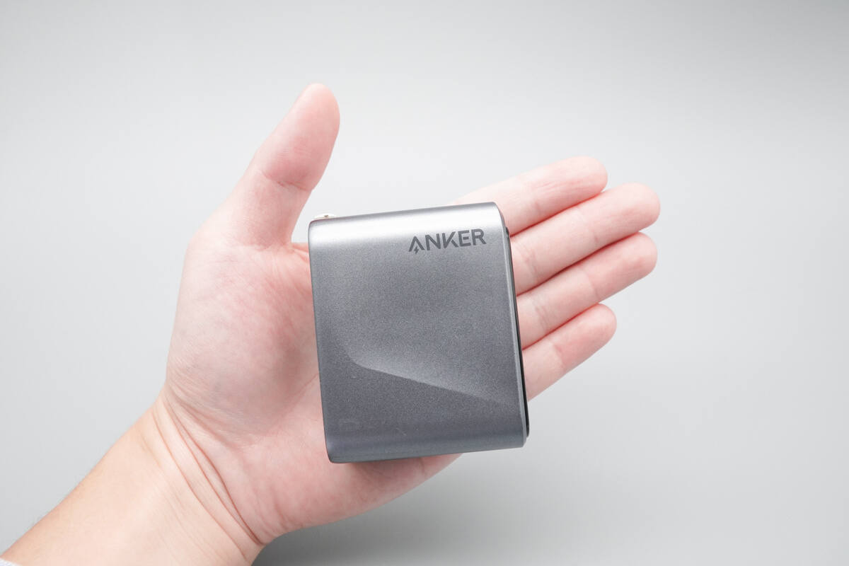
That's how big it is on the hand.
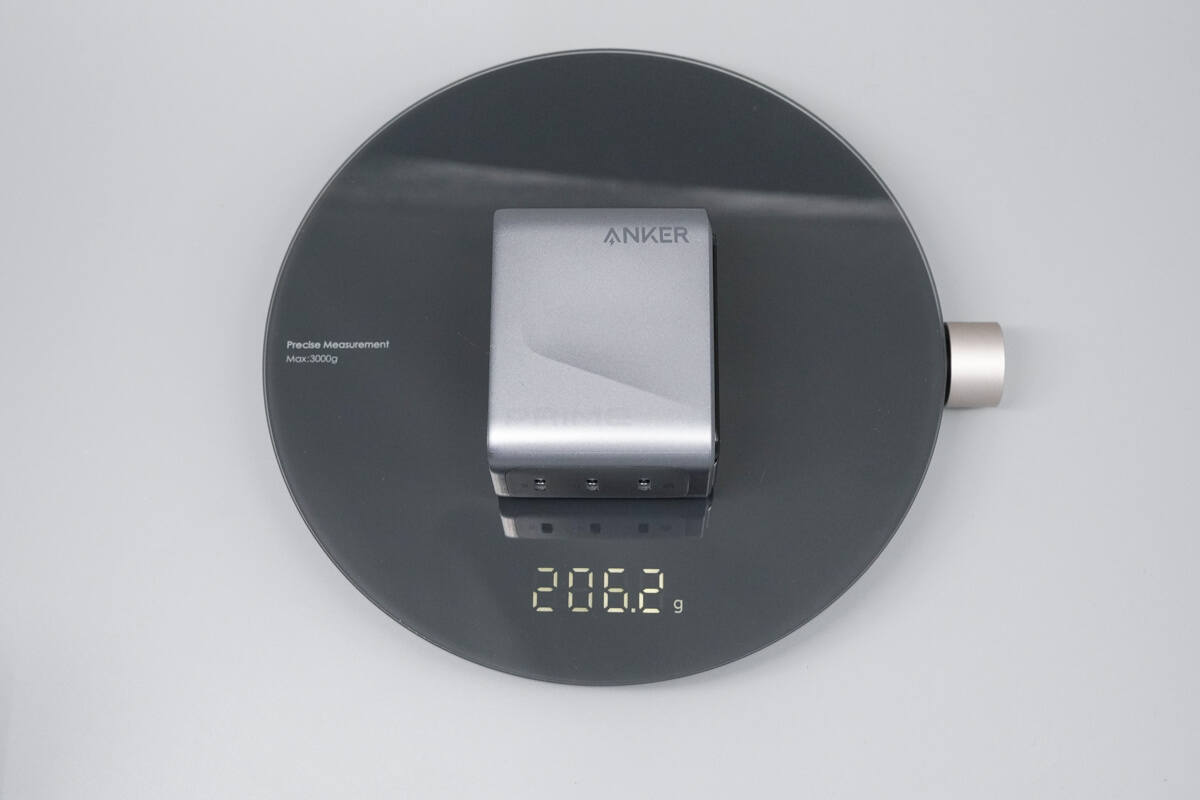
The weight is about 206 g (7.27 oz).
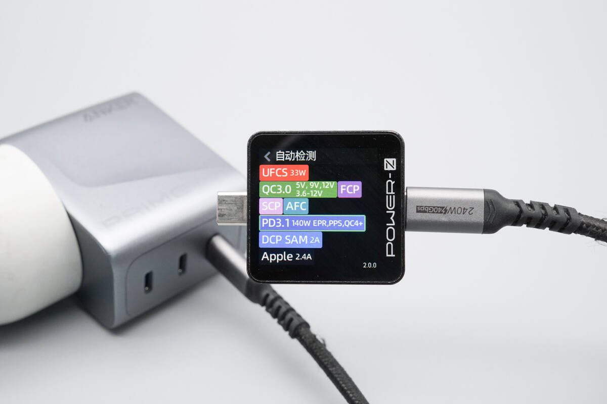
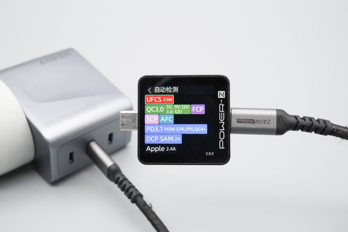
ChargerLAB POWER-Z KM003C shows that the USB-C1 supports QC3+/4+, FCP, SCP, AFC, PD3.1, PPS, DCP, SAM 2A, and Apple 2.4A charging protocols.
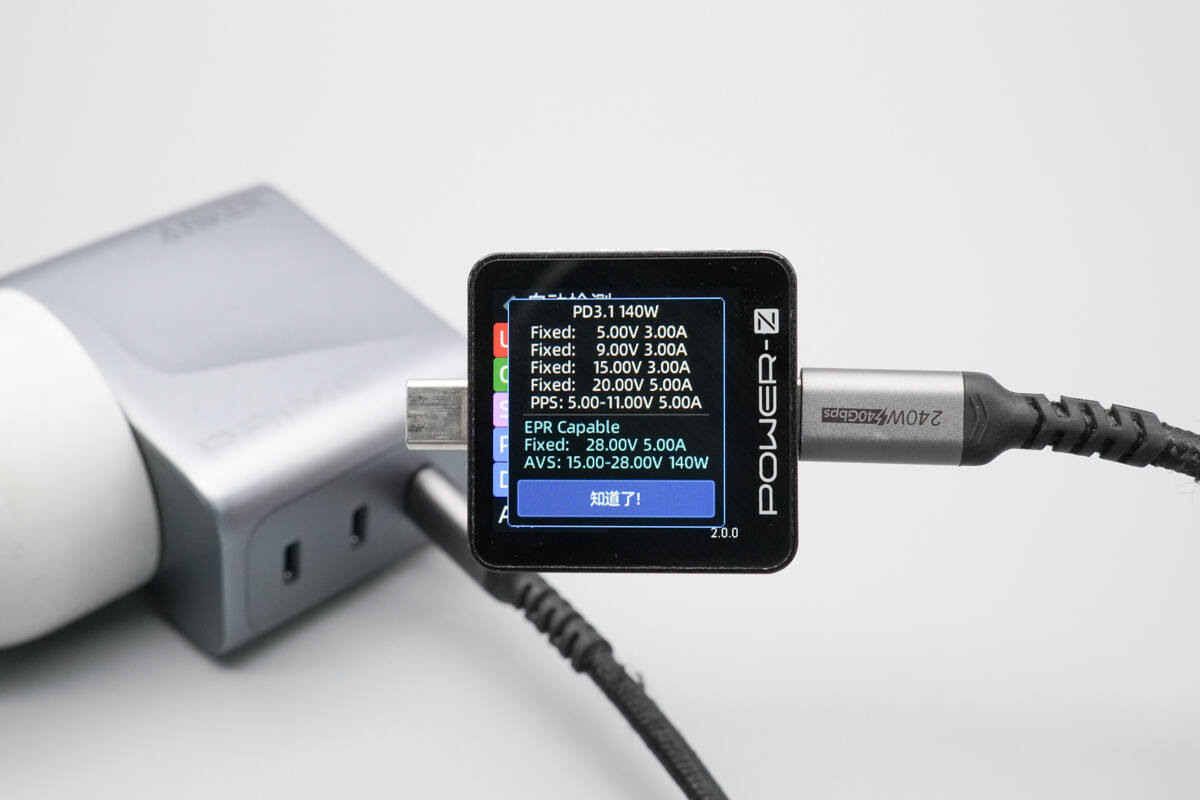
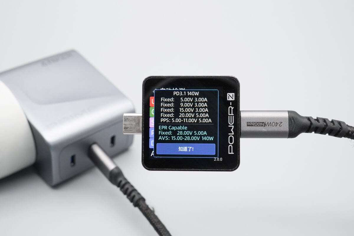
It has five fixed PDOs of 5V 3A, 9V 3A, 15V 3A, 20V 5A, and 28V 5A, as well as a PPS voltage range of 5–11V 5A and an AVS voltage range of 15–28V 140W.
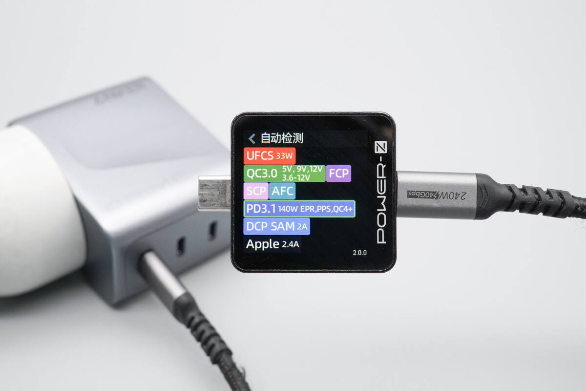
The USB-C2 port supports the same protocols as the USB-C1 port.
The PDO profiles are also identical.
The USB-C3 port supports the same protocols as the first two ports.
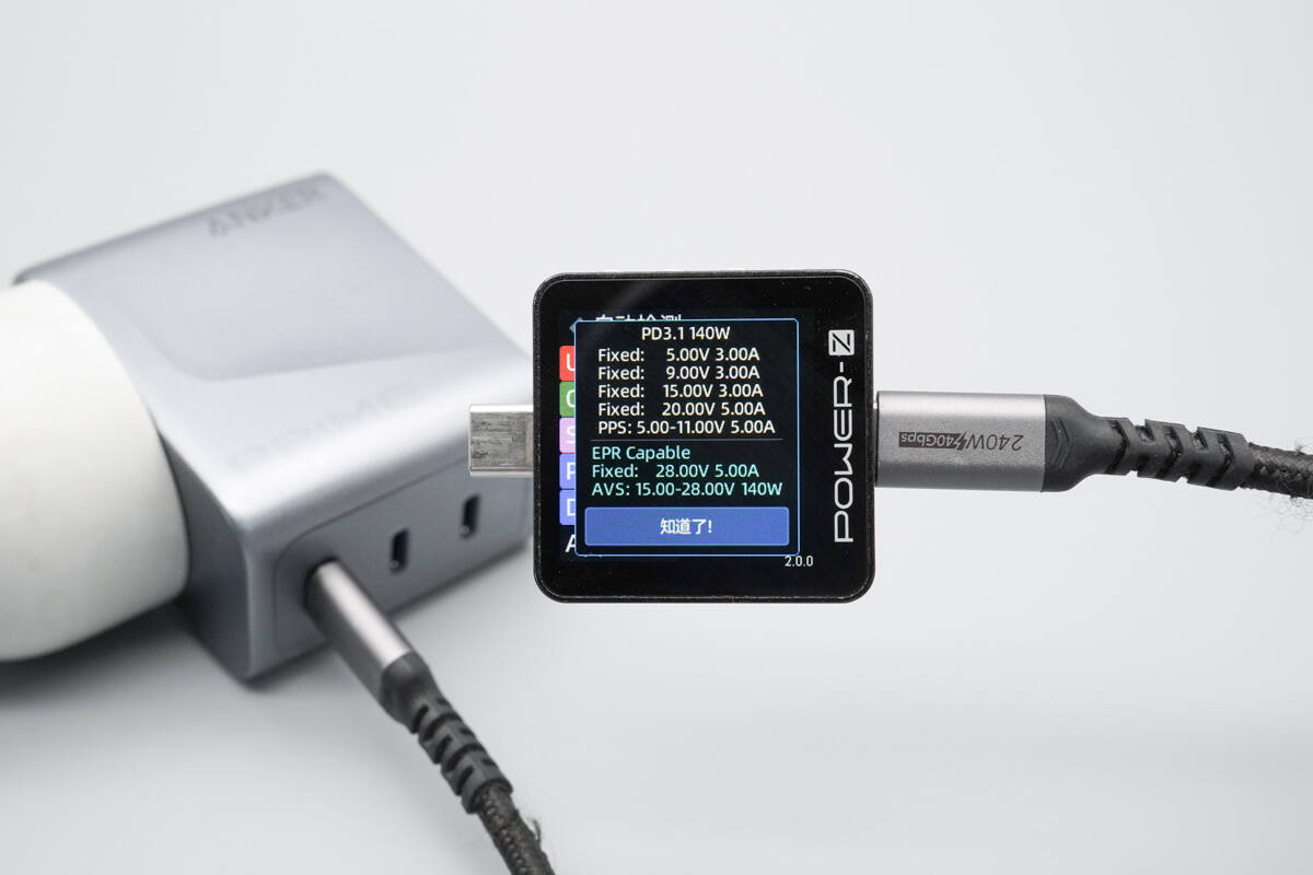
The PDO reports are identical as well.
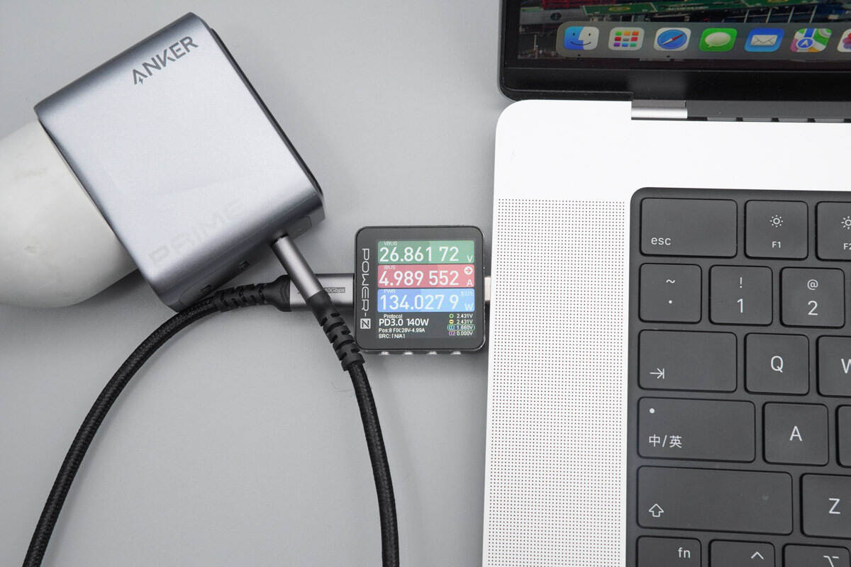
When used to charge a MacBook Pro, it delivers a charging power of about 134.02W.
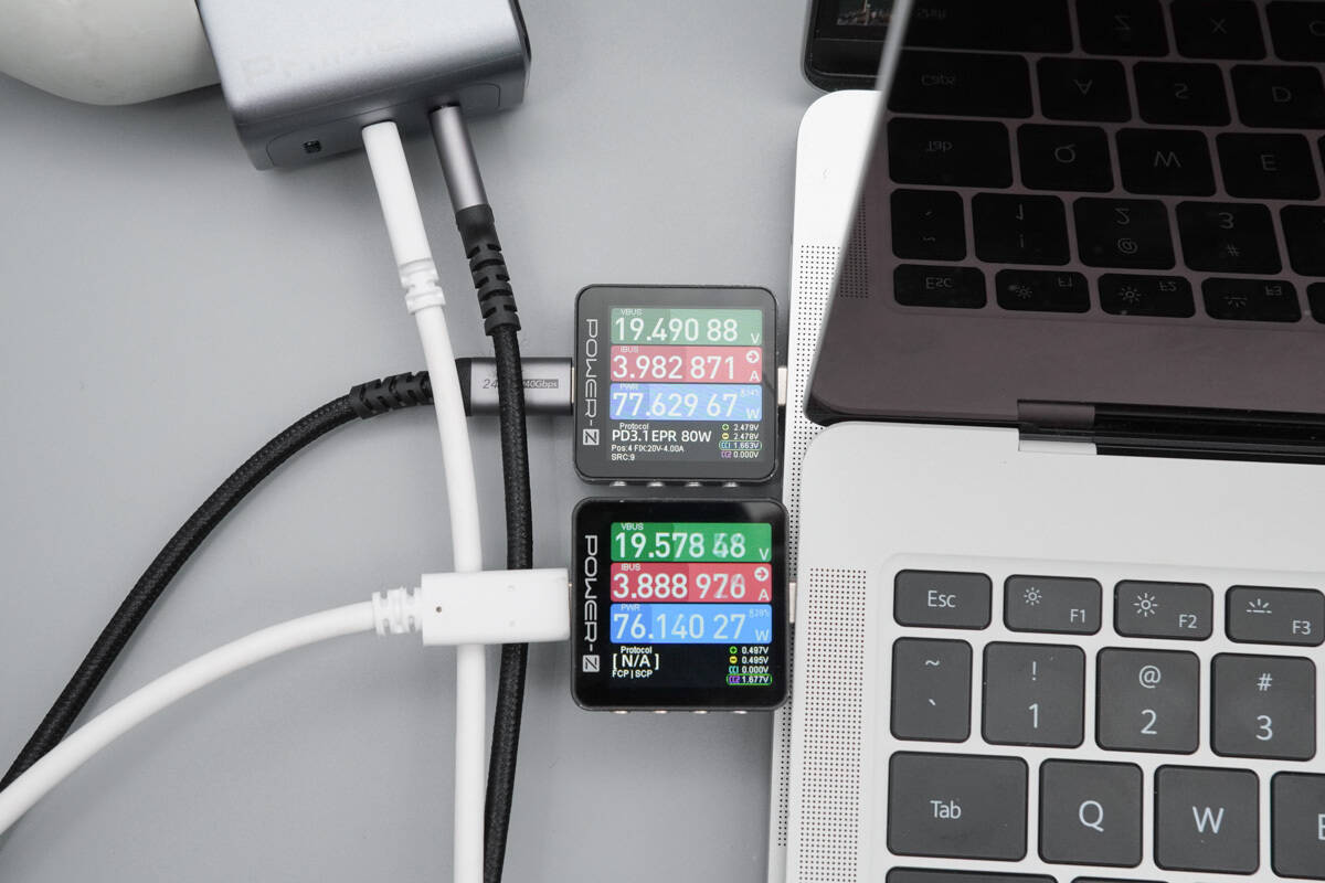
When charging two laptops simultaneously, the charging power is about 77.62W and 76.14W, with a total output of around 153.76W.
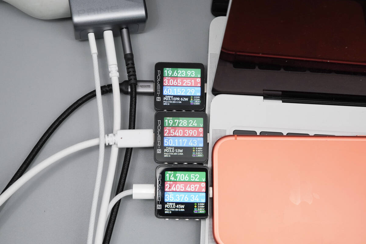
When charging two laptops and a smartphone simultaneously, the output power is about 60.15W, 50.12W, and 35.37W, with a total of around 145.64W.
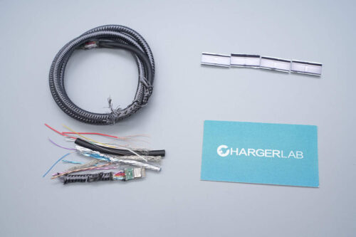
Teardown
Next, let's take it apart to see its internal components and structure.
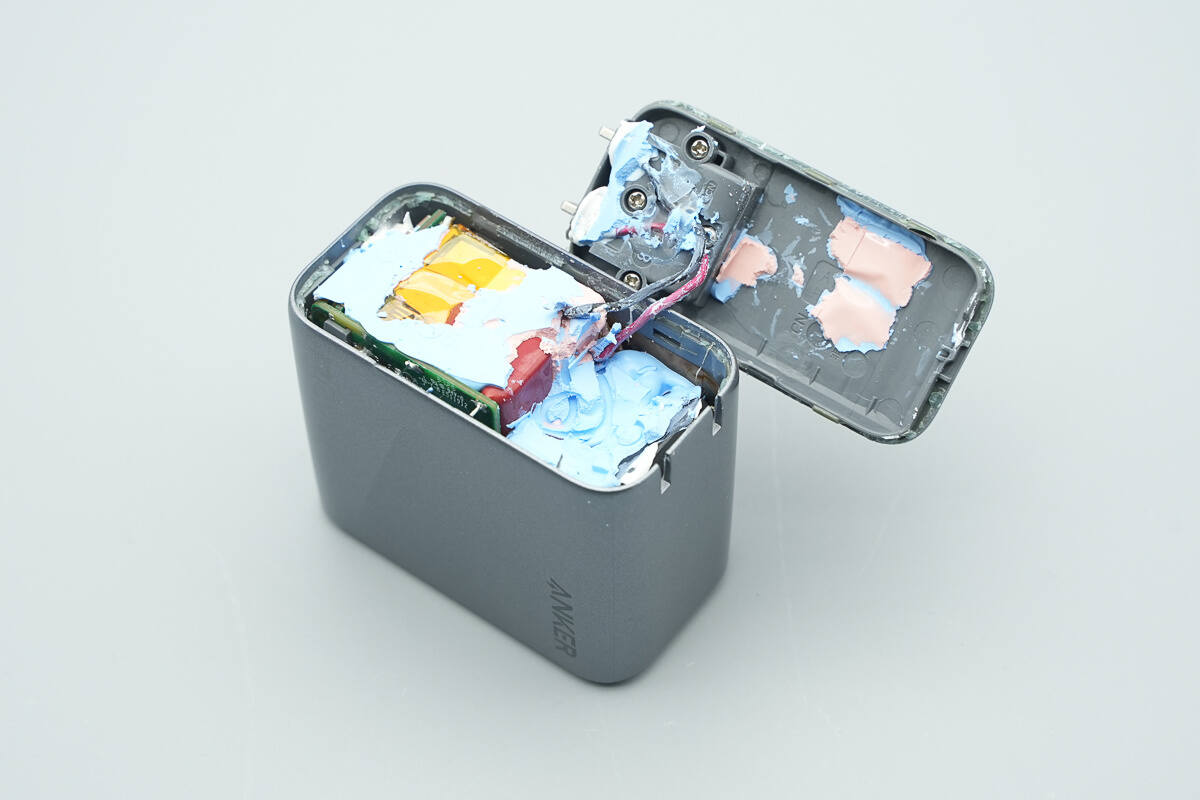
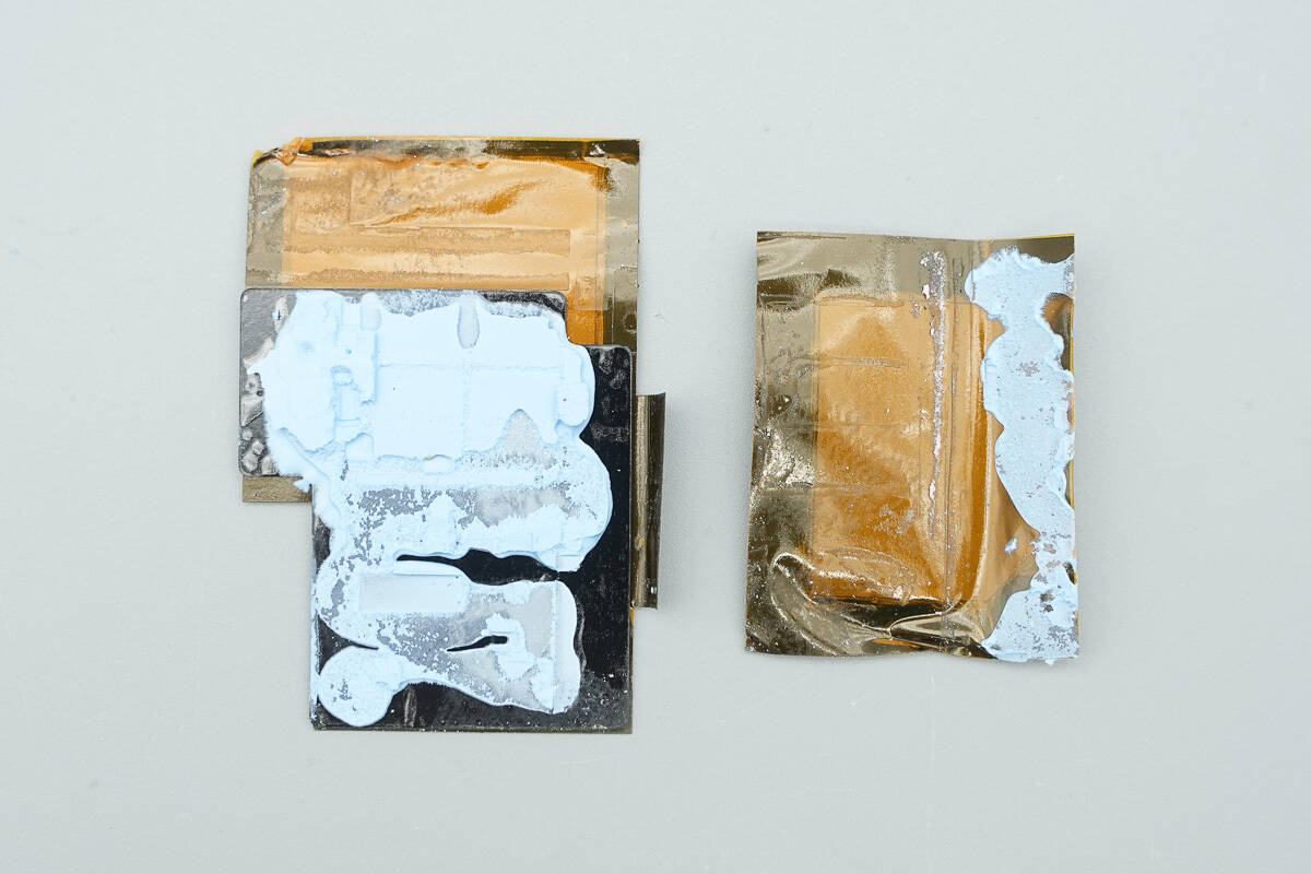
Open the input-side casing. The prongs are secured with a plastic plate and screws, and the internal module is filled with blue and pink thermal gel.
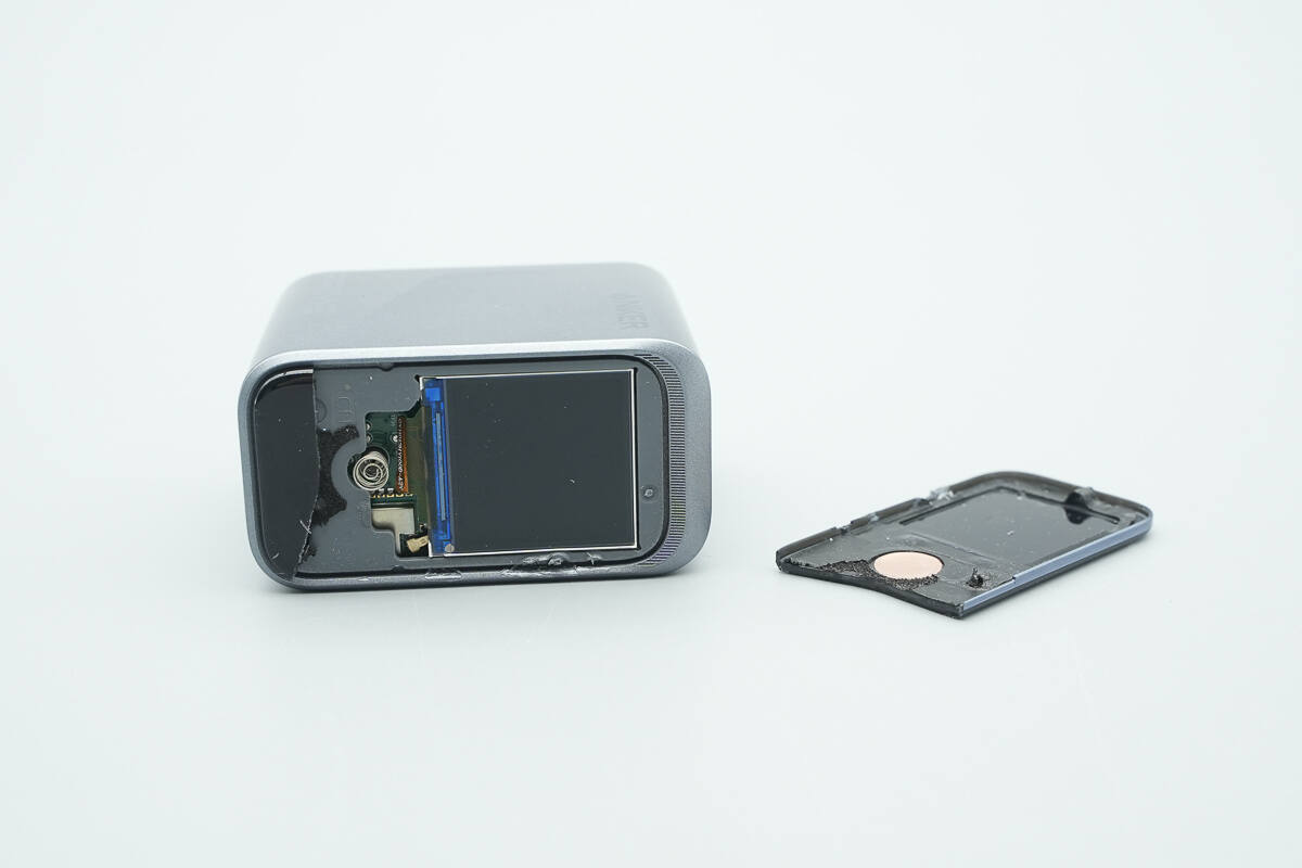
Removing the top cover reveals that it is secured with double-sided adhesive.
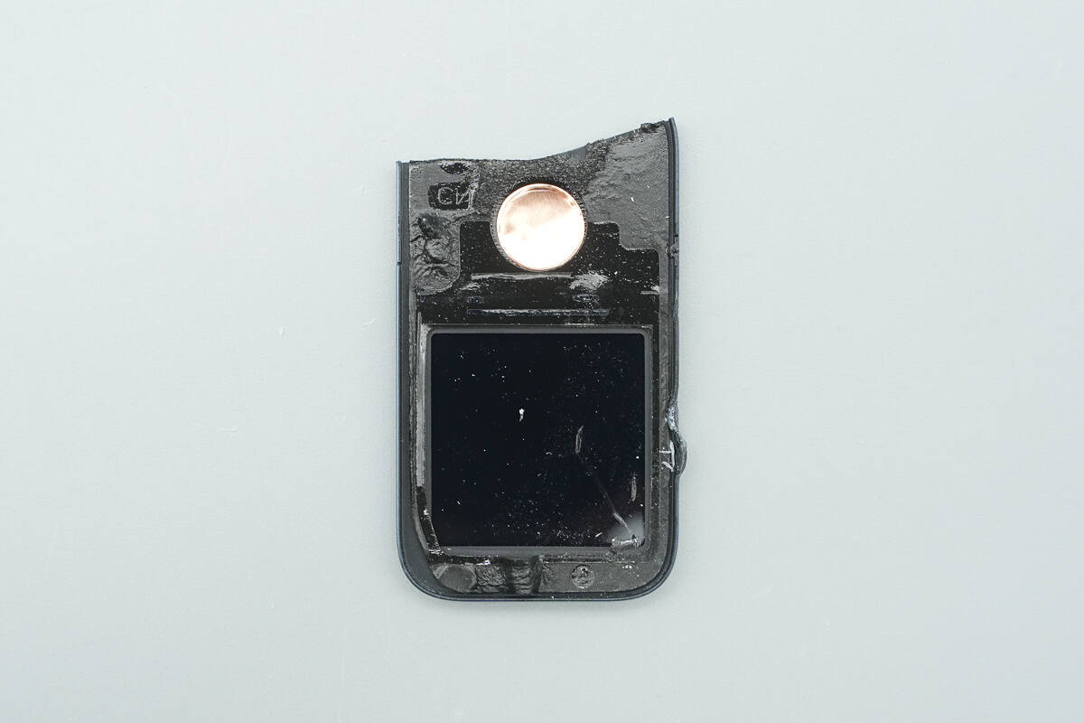
The cover has a window for the display, and copper foil is applied at the positions corresponding to the touch-sensitive button.
The display is connected to the PCBA module via a ribbon cable, and the bottom is protected with a layer of foam.
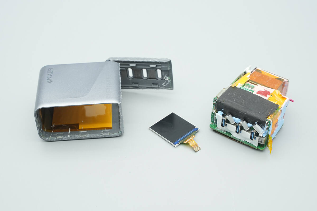
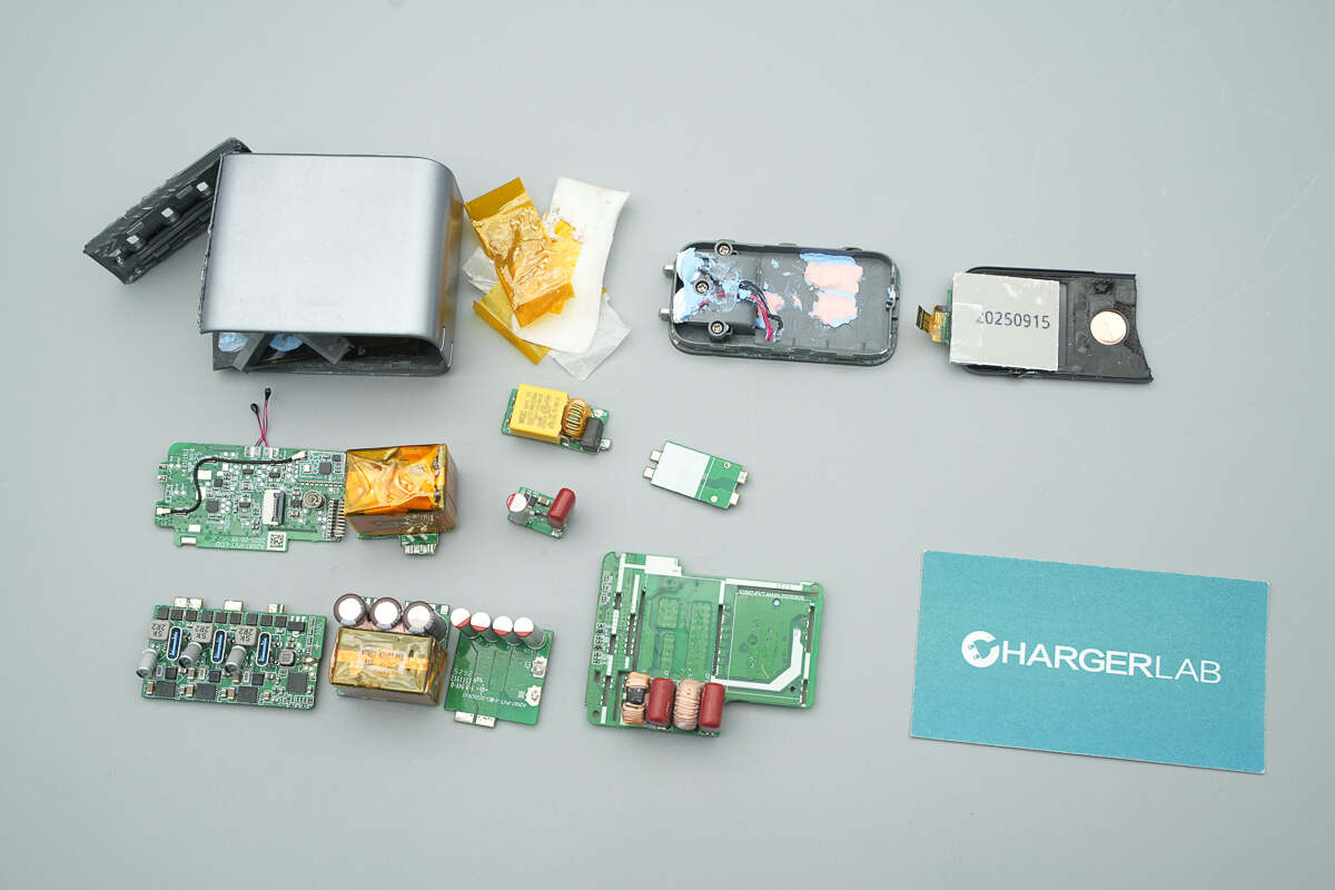
Cut open the casing to remove the PCBA module and the display.
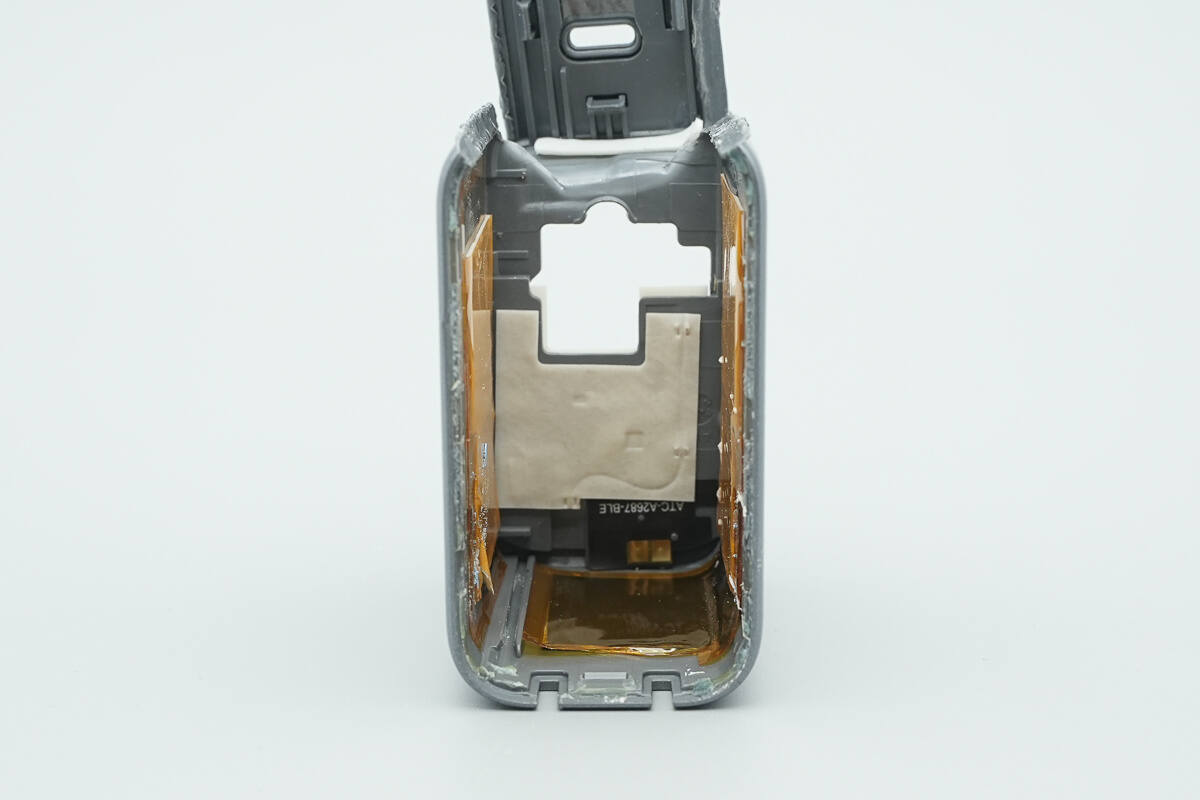
The inner side of the casing is lined with foam and graphite thermal pads and insulated with high-temperature-resistant tape.
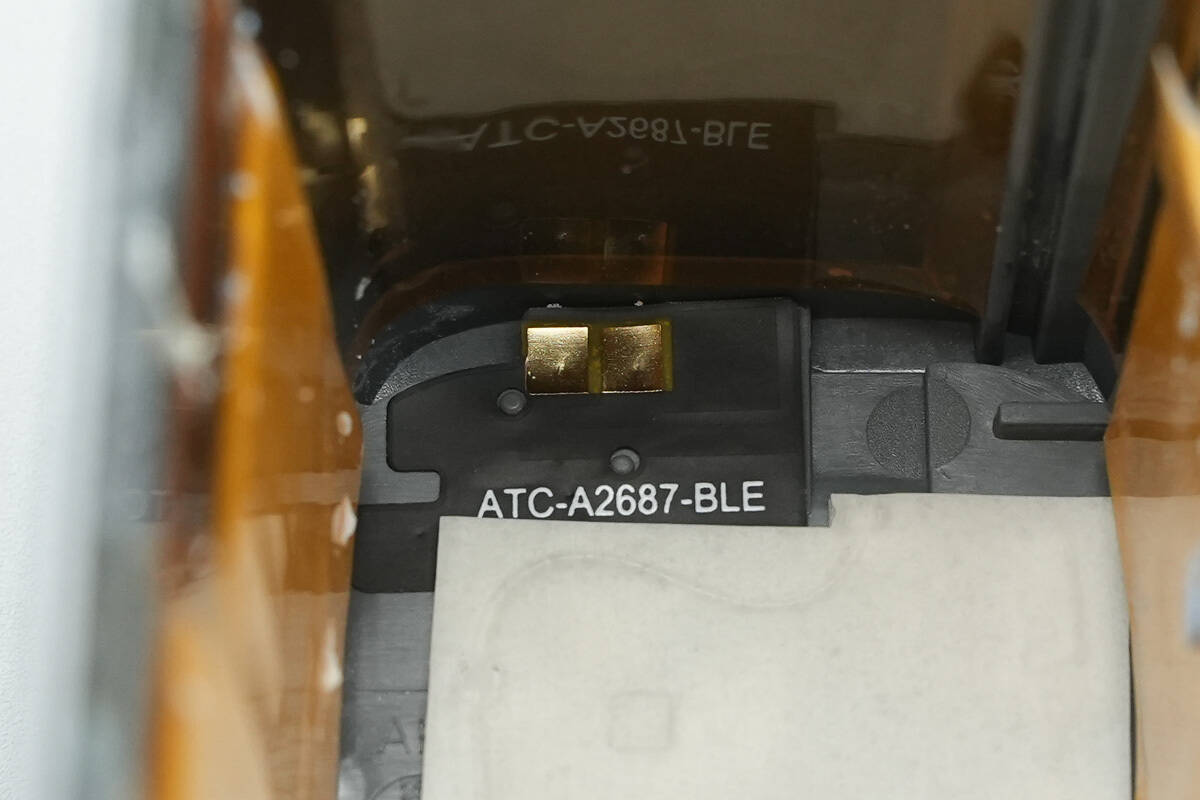
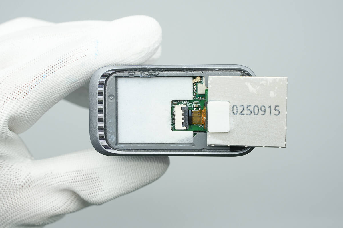
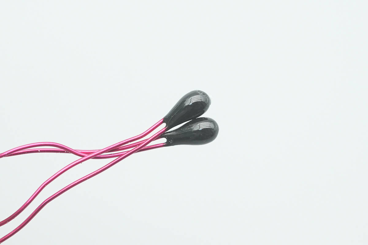
Close-up of the SMD Bluetooth antenna.
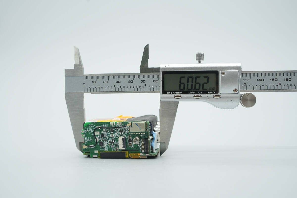
The length of the PCBA module is about 60.62 mm (2.39 inches).
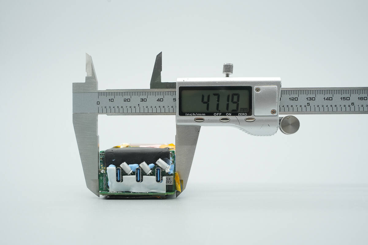
The width is about 47.19 mm (1.86 inches).
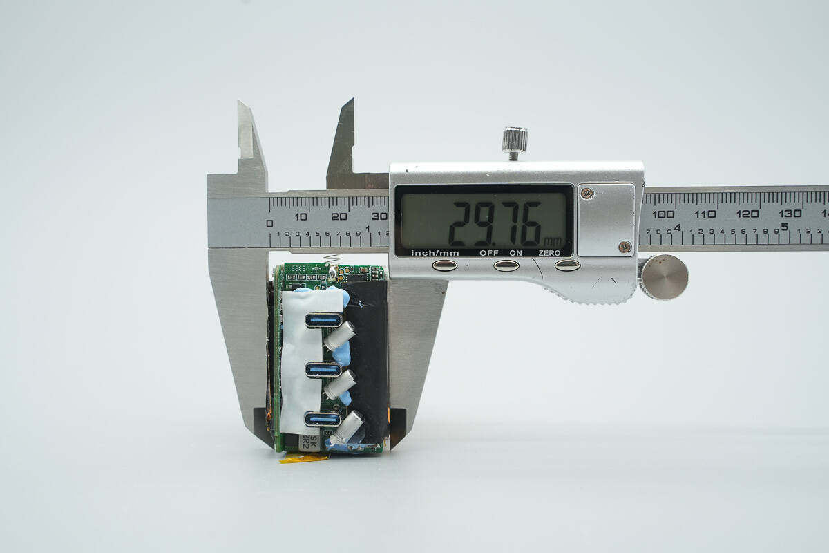
The thickness is about 29.76 mm (1.17 inches).
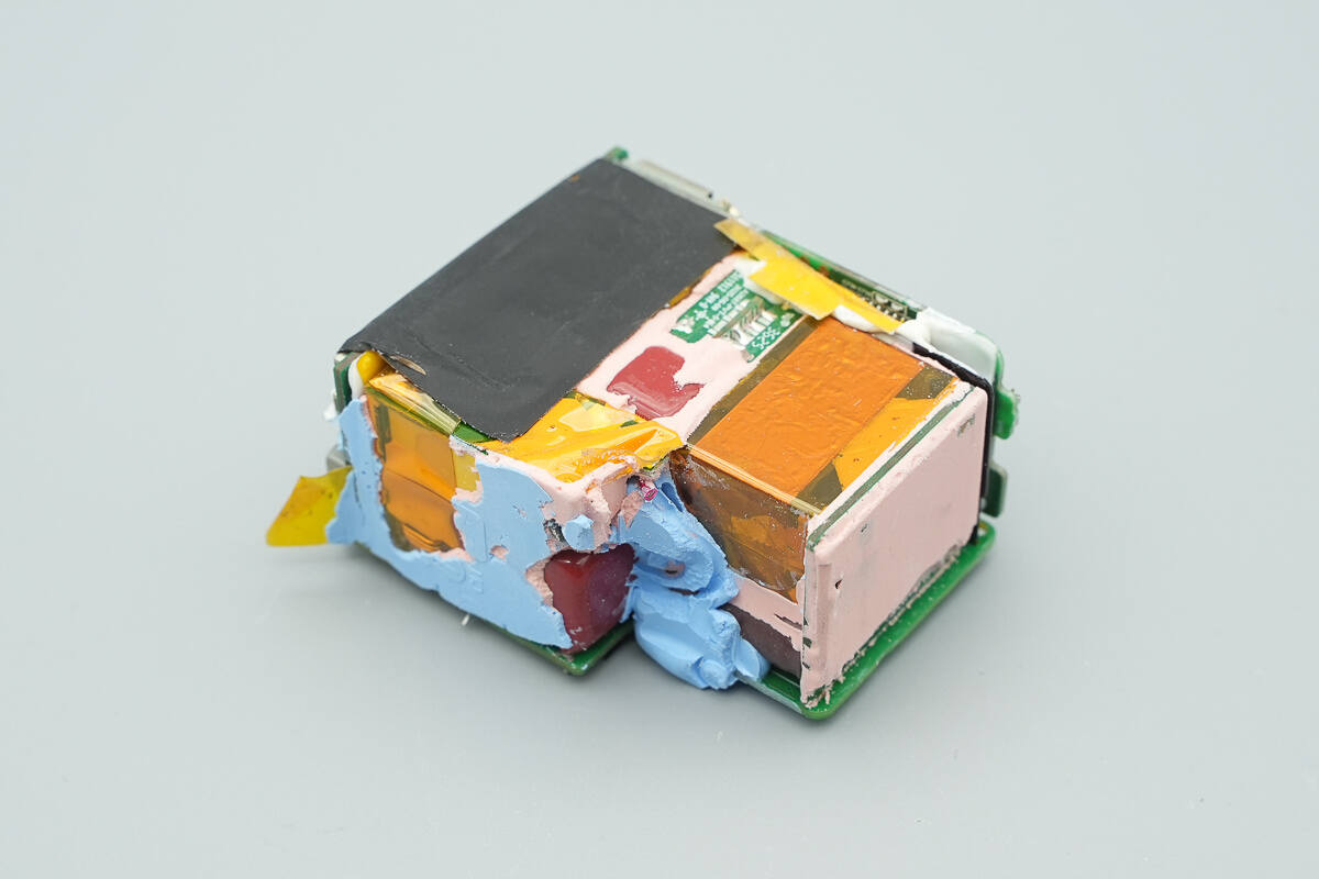
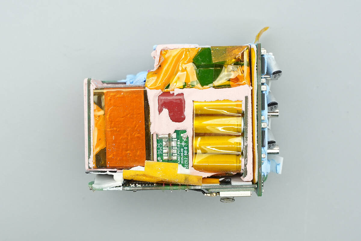
The gaps between components are filled with thermal adhesive, and one side of the module is covered with an insulated thermal pad.
The bottom of the module is also covered with an insulated thermal pad.
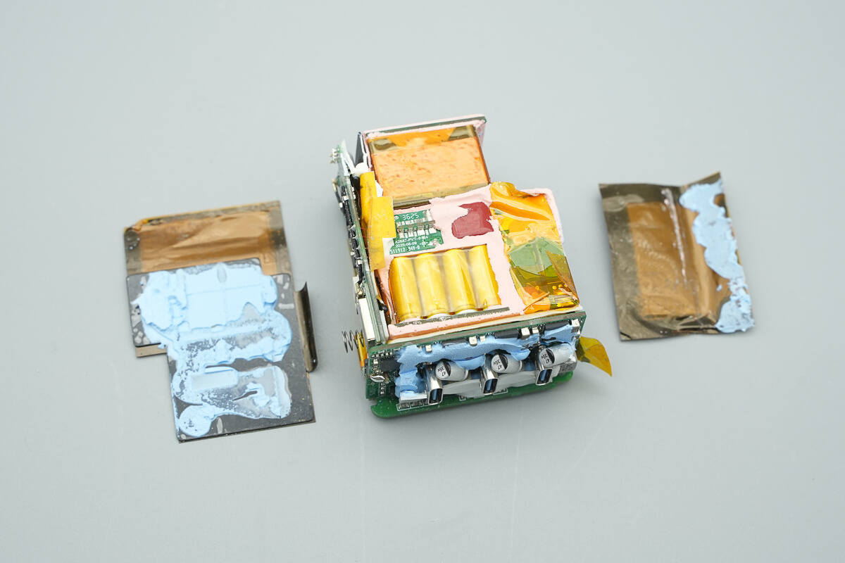
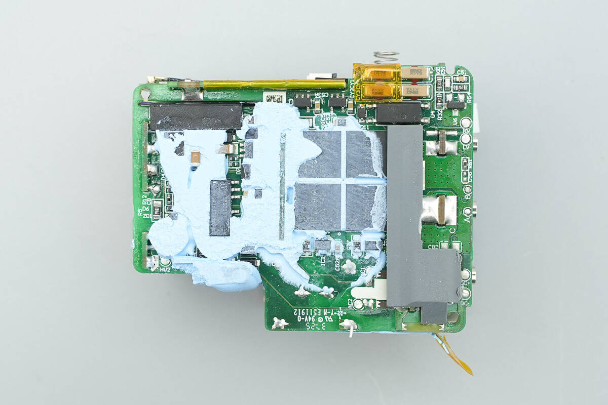
Remove the thermal pad; a Mylar sheet is found between it and the motherboard for insulation.
The thermal pads are composed of copper foil and graphite, with both sides insulated.
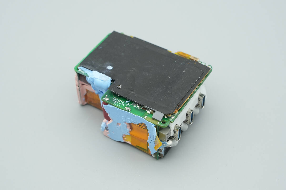
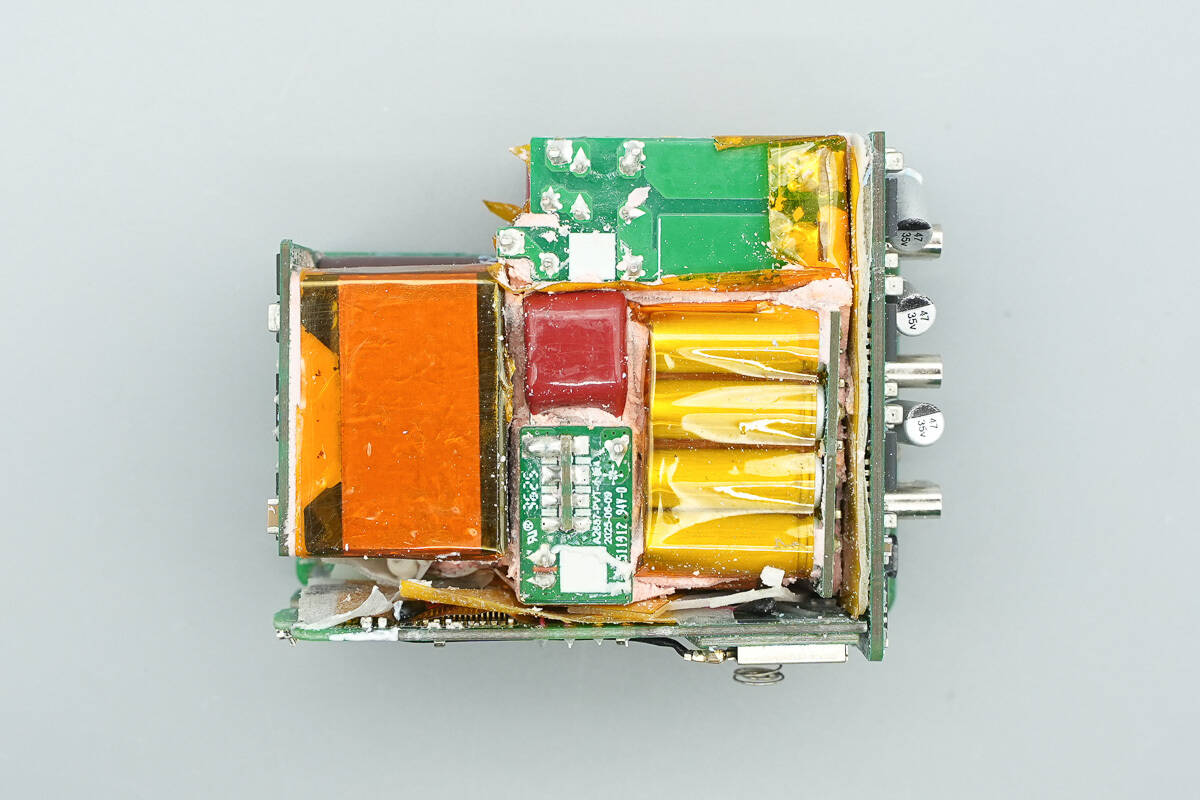
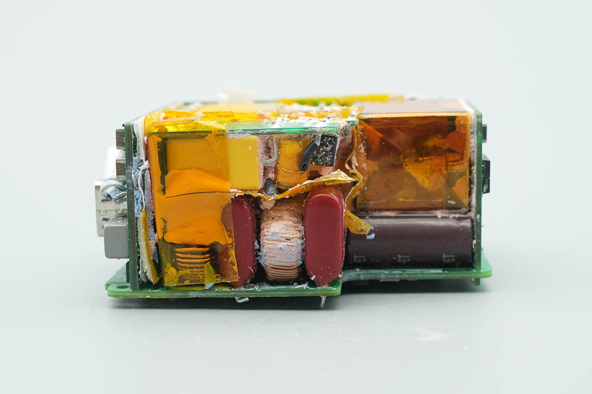
On the front of the PCBA module, the input small PCB, the PFC boost inductor, and solid capacitors for output filtering are all wrapped with insulating tape.
The back side is filled with thermal adhesive, while the side openings are fitted with plastic isolation plates and Mylar sheets for insulation protection.
Remove the thermal adhesive. The PCBA module consists of as many as nine PCBs, arranged compactly yet with thorough insulation measures in place.
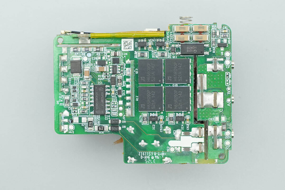
The back side houses active bridge drivers, rectifiers, and the master control chip, among other components.
At the input end, there is a small PCB. On the main PCB, there are film capacitors, filter inductors, and a small PCB used for structural support.
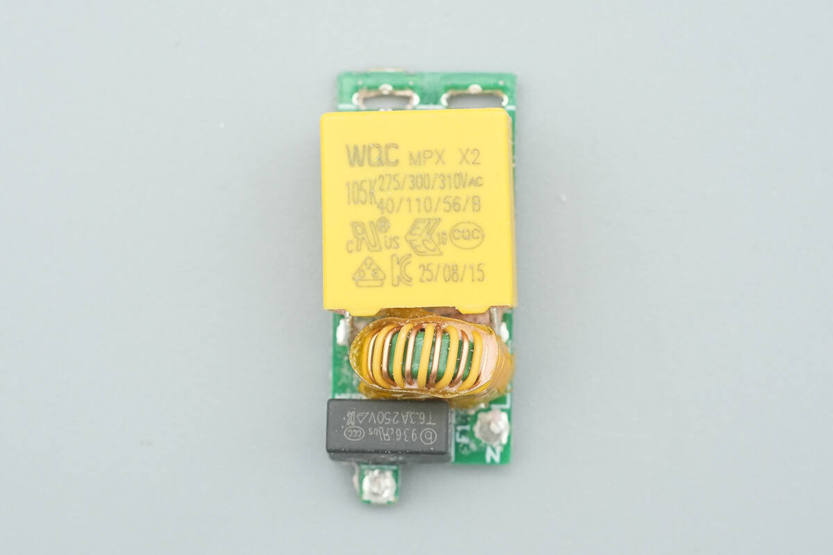
After removing the two small PCBs, the input PCB reveals a time-delay fuse, a common-mode choke, and a safety X2 capacitor.
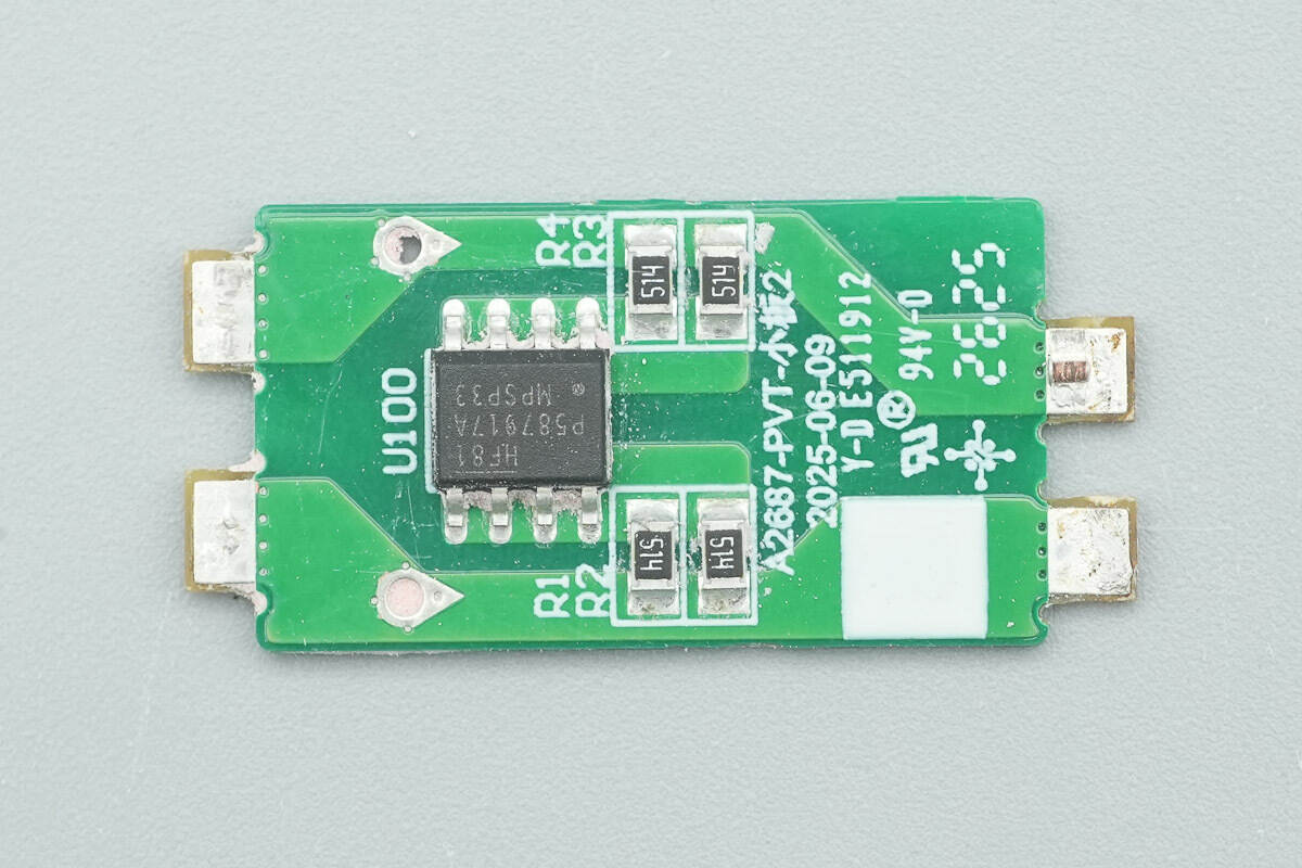
On the front of the support PCB, there is an X-capacitor discharge chip.
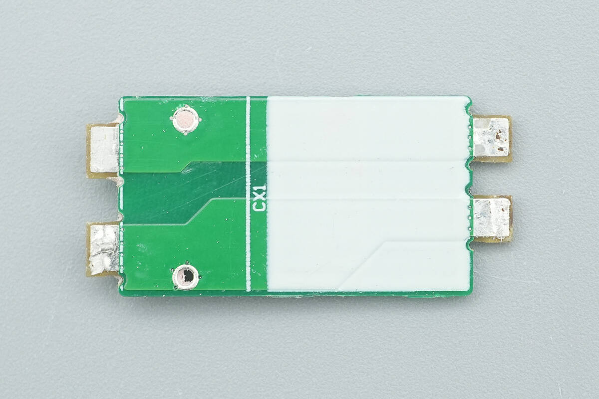
The back side has no components.
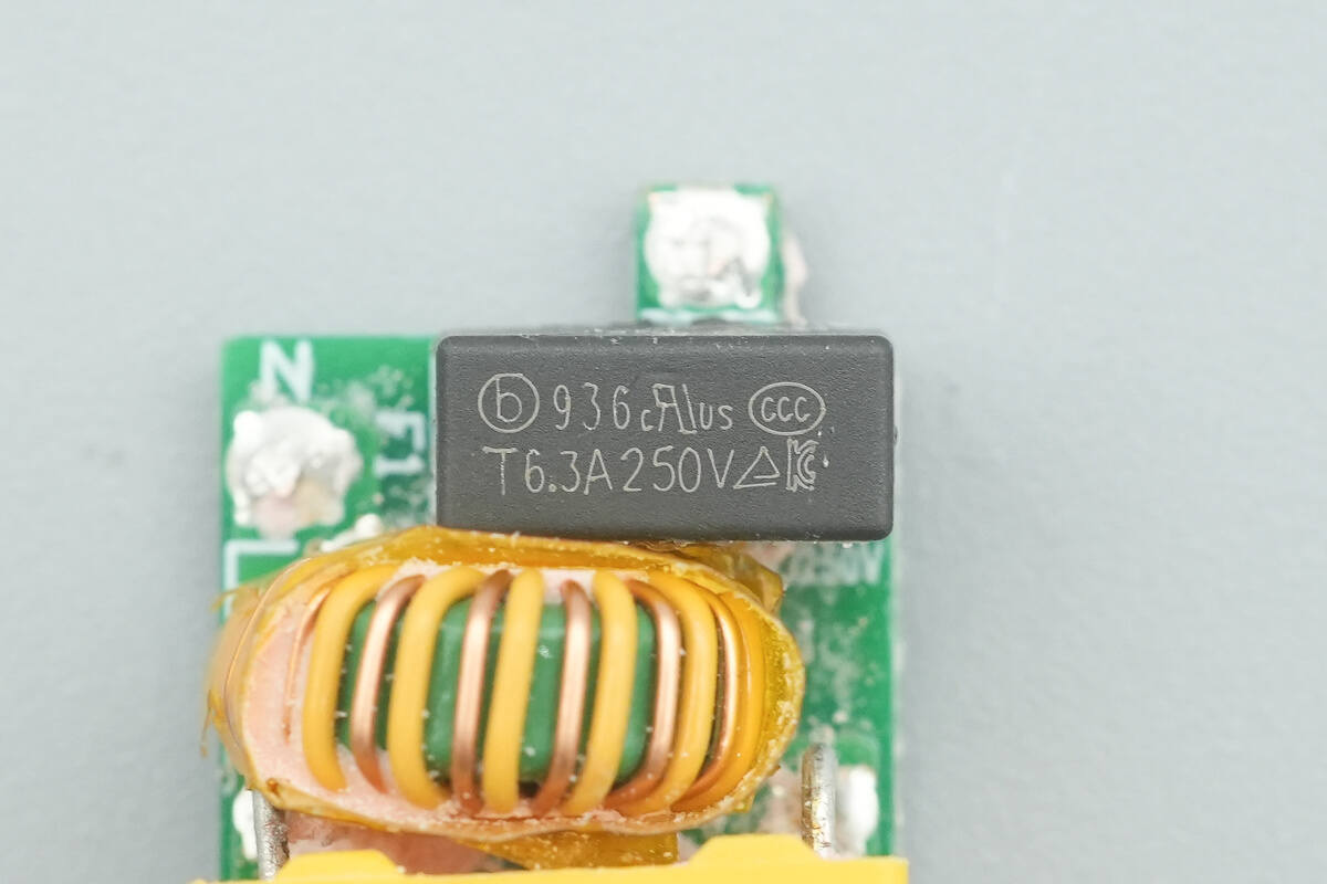
The time-delay fuse is from Betterfuse, rated at 6.3A 250V.
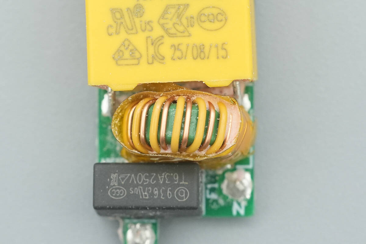
The common-mode choke, used to filter EMI interference, is wrapped in insulating tape.
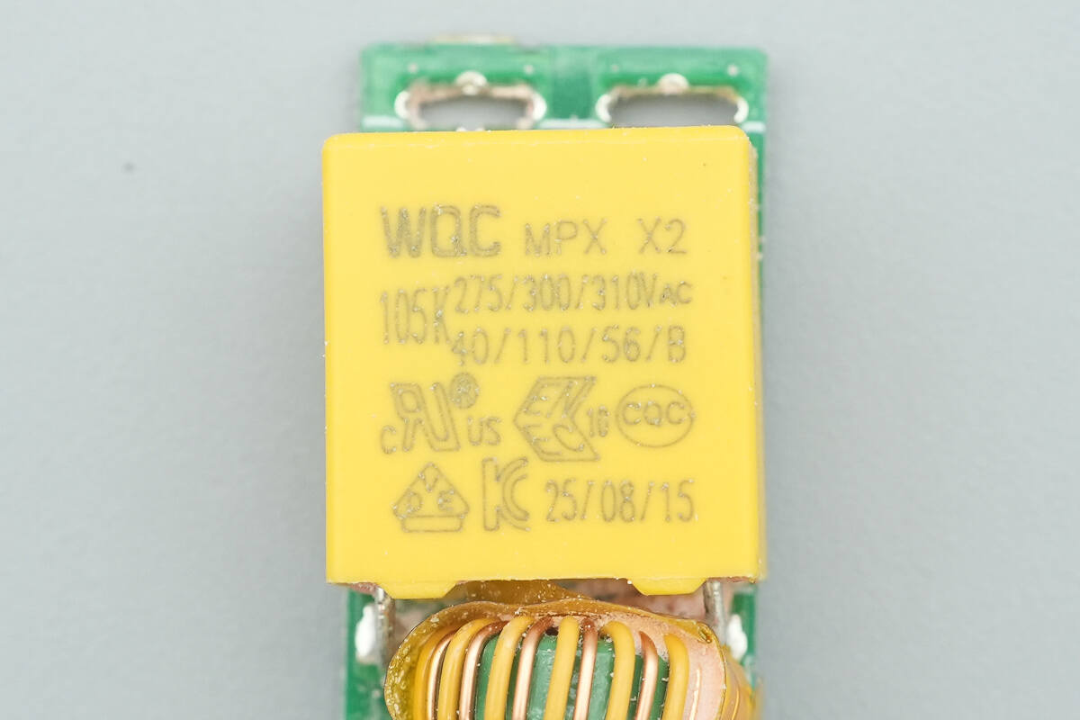
The safety X2 capacitor is from WQC, with a capacitance of 1 µF.
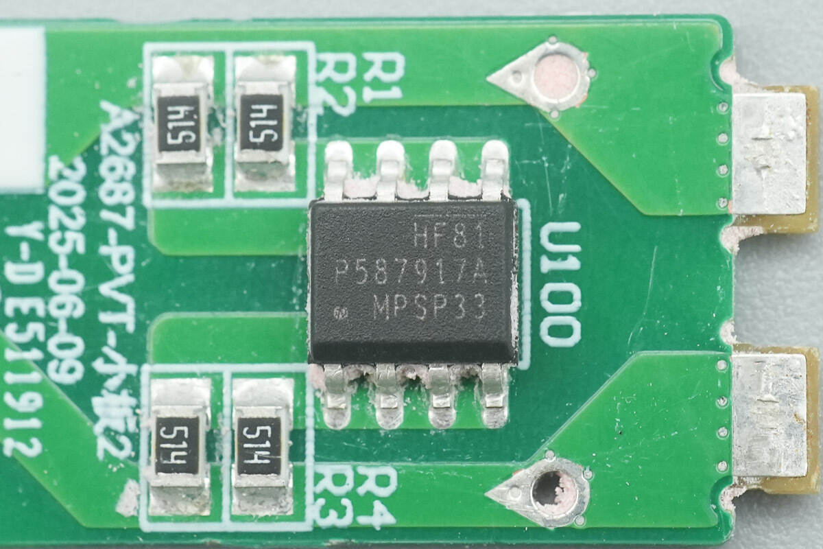
The X-capacitor discharge chip is from MPS, model HF81. This is an innovative two-terminal IC that can automatically discharge X capacitors while avoiding power loss and ensuring the power supply meets safety standards. It comes in an SOIC-8 package.
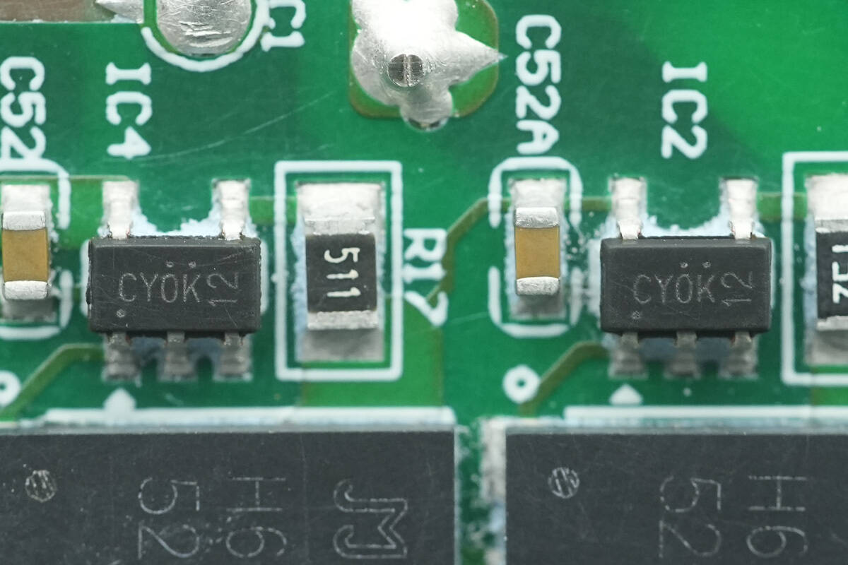
The active bridge drivers are from AOS, model AOZ7200CI. This is a 600V AlphaZBL™ series device designed to control external N-channel MOSFETs in AC/DC rectifier bridge applications, replacing traditional diodes to effectively reduce system power loss and thermal load.
In rectifier bridge applications, the AOZ7200CI minimizes the forward conduction loss of the external MOSFET by detecting the voltage difference across its terminals. During reverse current, it quickly turns off the MOSFET to withstand reverse voltage, thereby emulating the unidirectional conduction characteristic of an “ideal diode.”
In AC/DC applications, the chip uses a self-powered design, requiring no additional auxiliary power supply. The AOZ7200CI comes in a SOT23-5 package, with a rated operating temperature range of –40°C to +125°C.
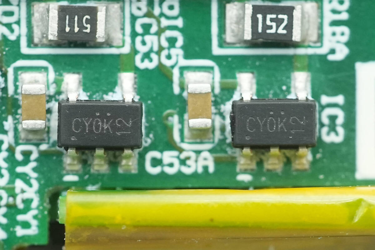
Close-up of the other two AOS AOZ7200CI active bridge drivers.
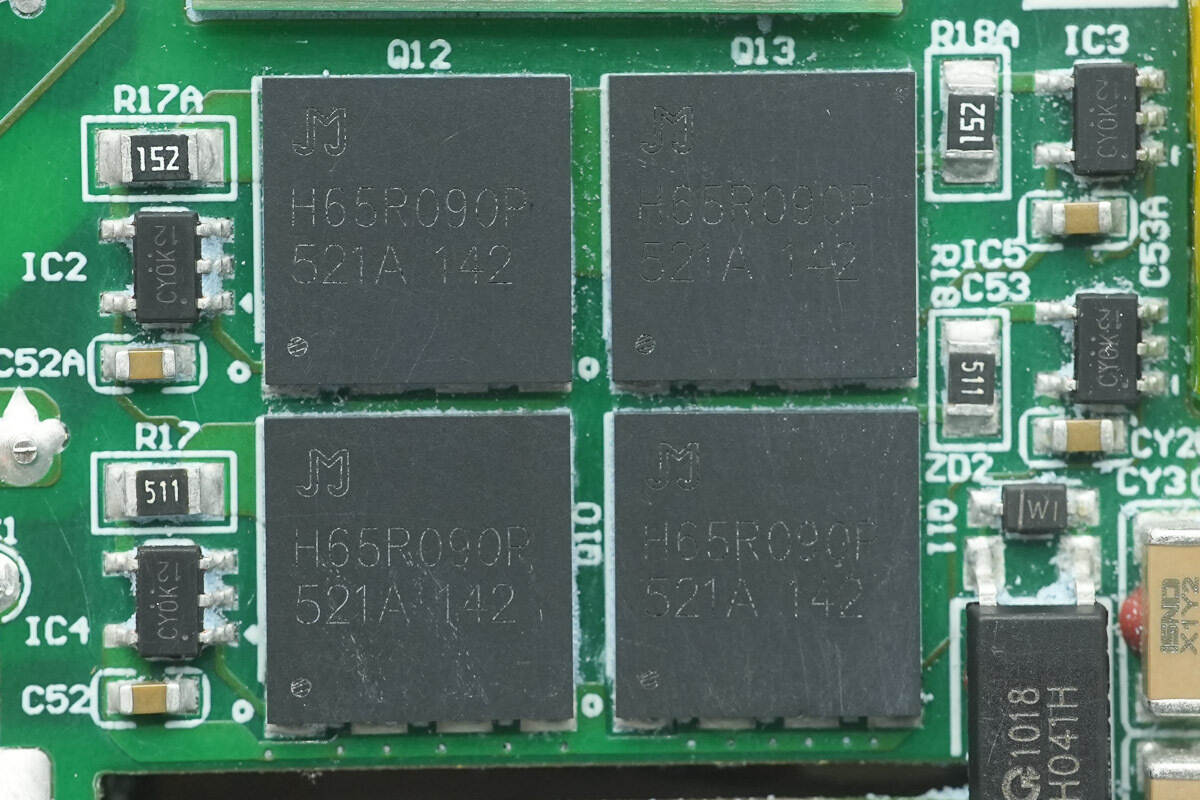
The four accompanying N‑MOSFETs are from JJWD, model JMH65R090PPLNFD, in a DFN8080‑4L package.
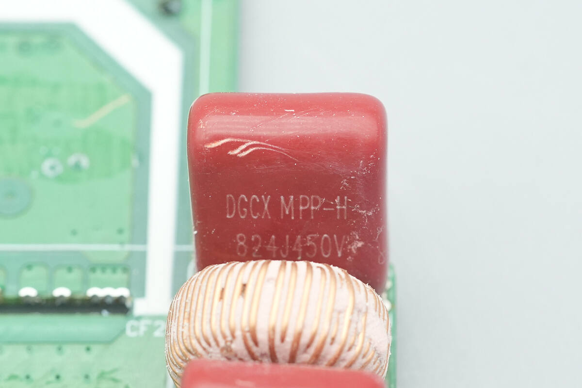
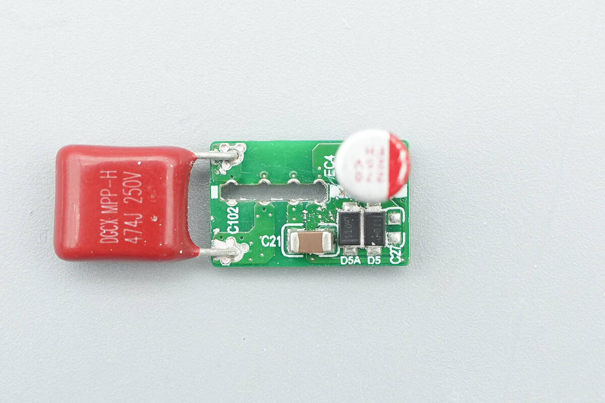
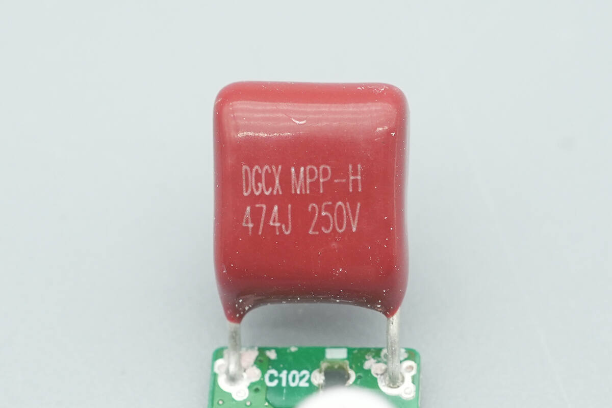
The film capacitors are from DGCX, rated at 0.82 µF, 450 V.
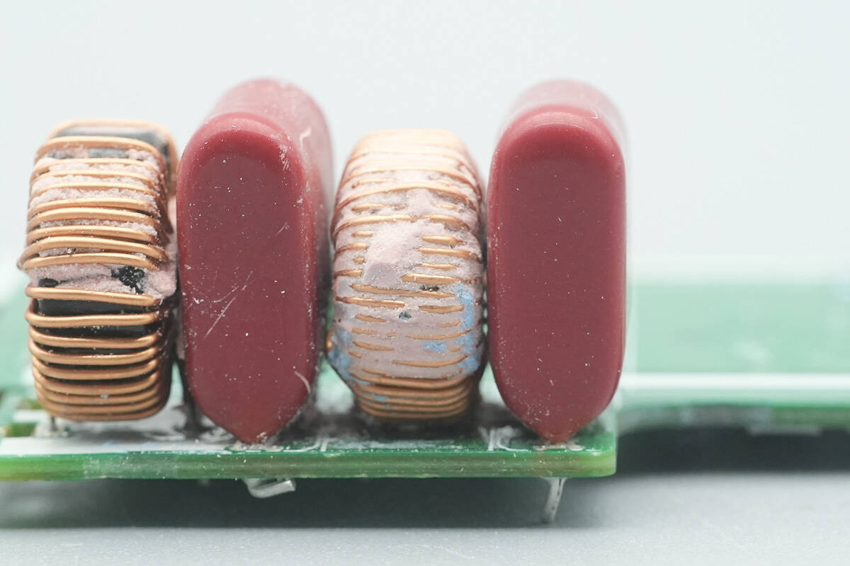
Close-up of the filter inductor.
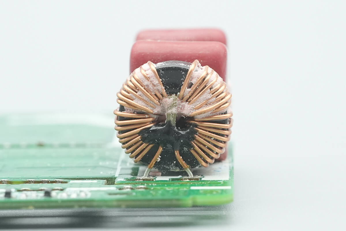
Close-up of the other filter inductor.
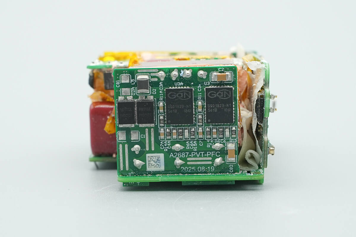
On this side is the PFC boost small PCB. The back of the PFC boost PCB houses the PFC MOSFETs and PFC boost rectifiers.
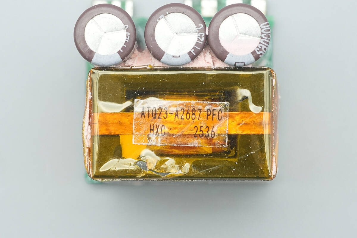
After removing the PCB, the other side features the PFC boost inductor and three high-voltage filter electrolytic capacitors.
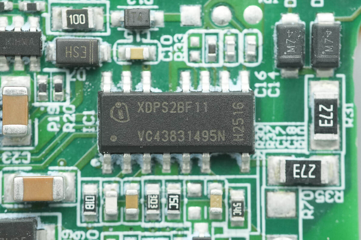
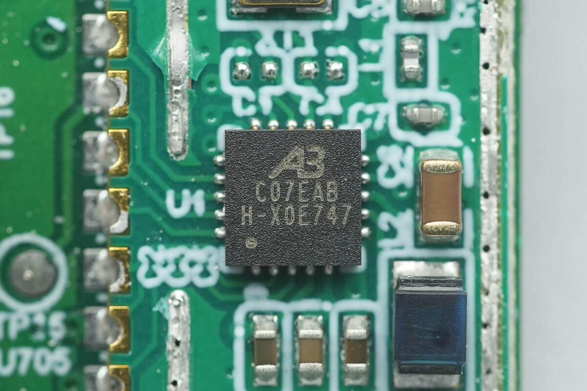
The master control chip is from Infineon, marked XDPS2BF11. It is a custom model that integrates both the PFC controller and the HFB controller, and comes in a DSO-14 package.
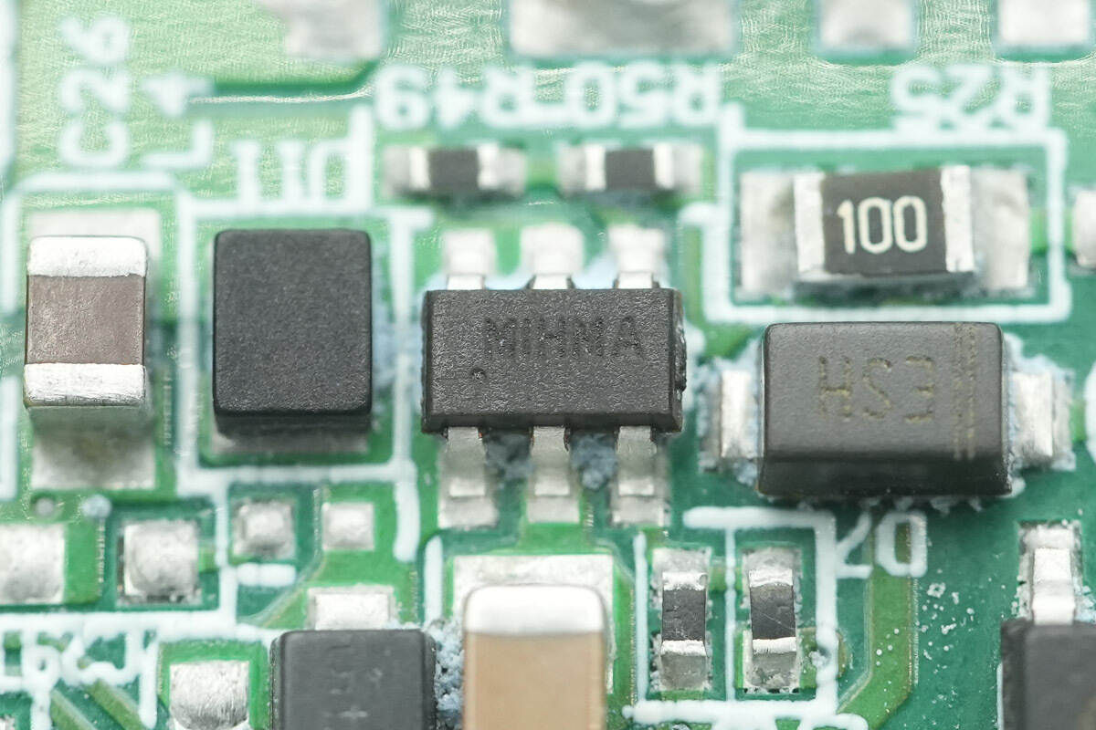
A chip marked MIHMA.
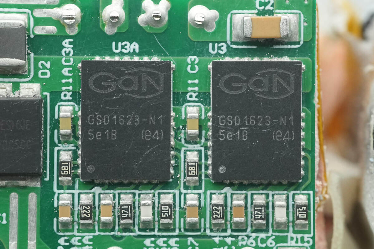
The PFC MOSFETs are from Infineon, model GSD1623‑N1. This is a 150 mΩ enhancement-mode GaN transistor with integrated smart gate drive and lossless current-sensing features, housed in a VIQFN‑30 package.
The PFC boost inductor is tightly wrapped with tape.
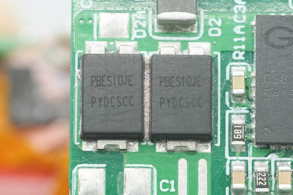
The PFC rectifiers are from PY, marked PBES10JE. They are 10 A, 600 V ultra-fast recovery diodes.
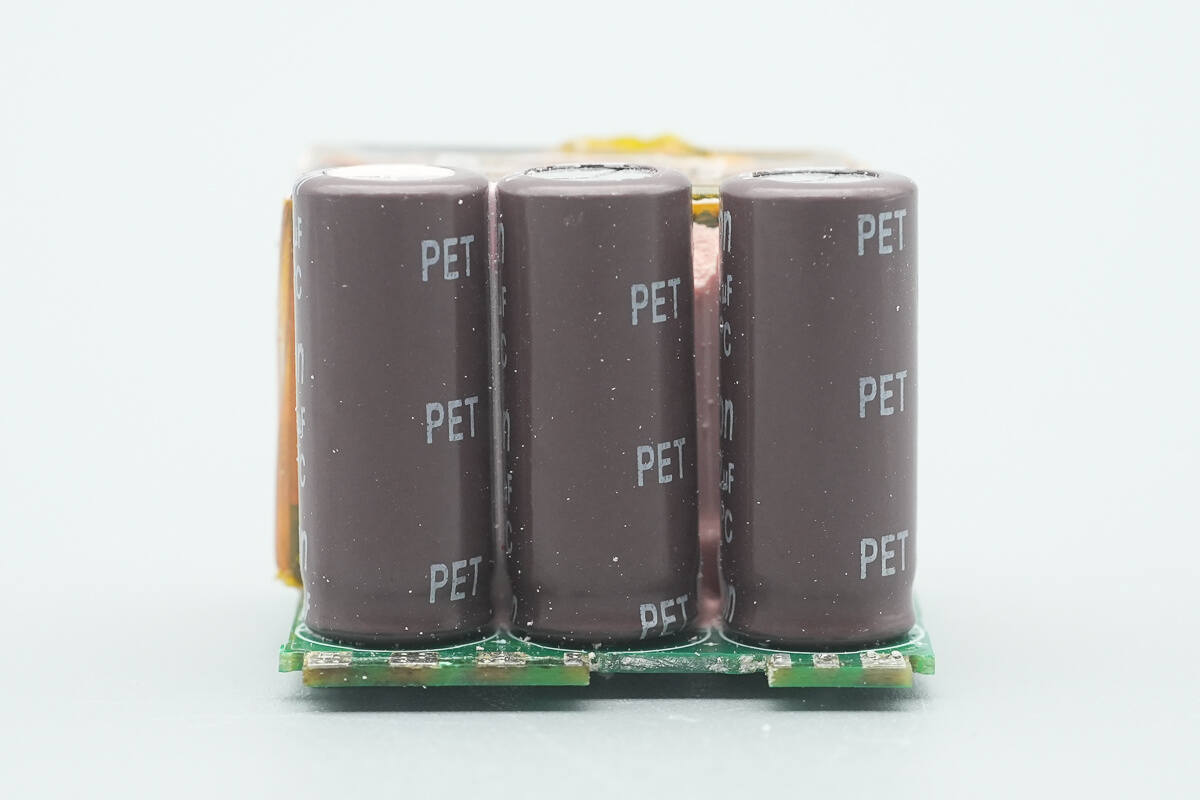
All three electrolytic capacitors share the same part number.
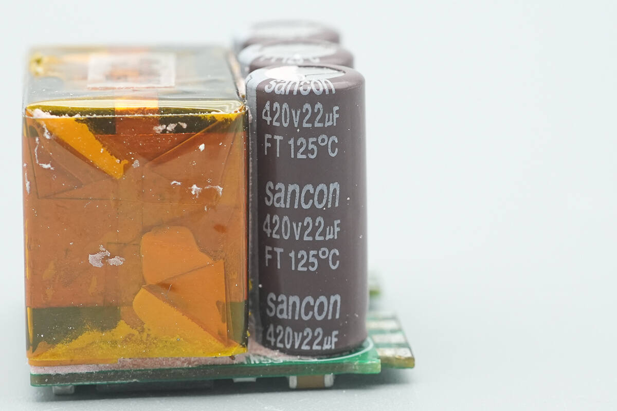
The capacitors are from Sancon, each rated at 420 V, 22 µF.
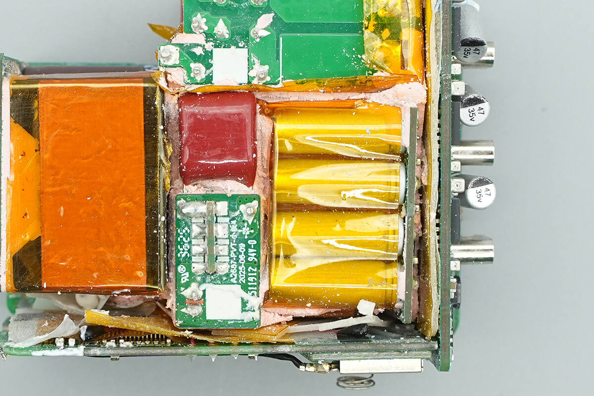
On the front of the PCBA module, there is a small PCB at the top center, a small support PCB below it, and a small synchronous rectification PCB on the right side.
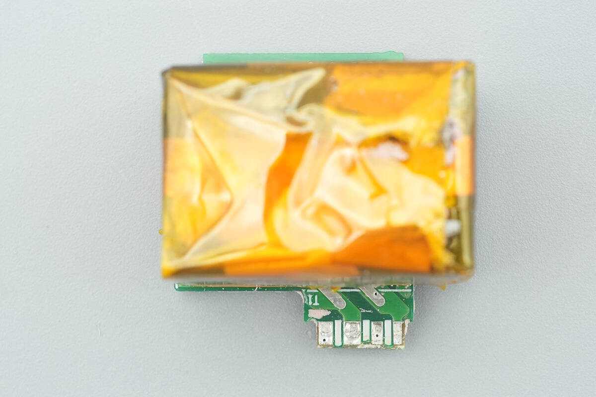
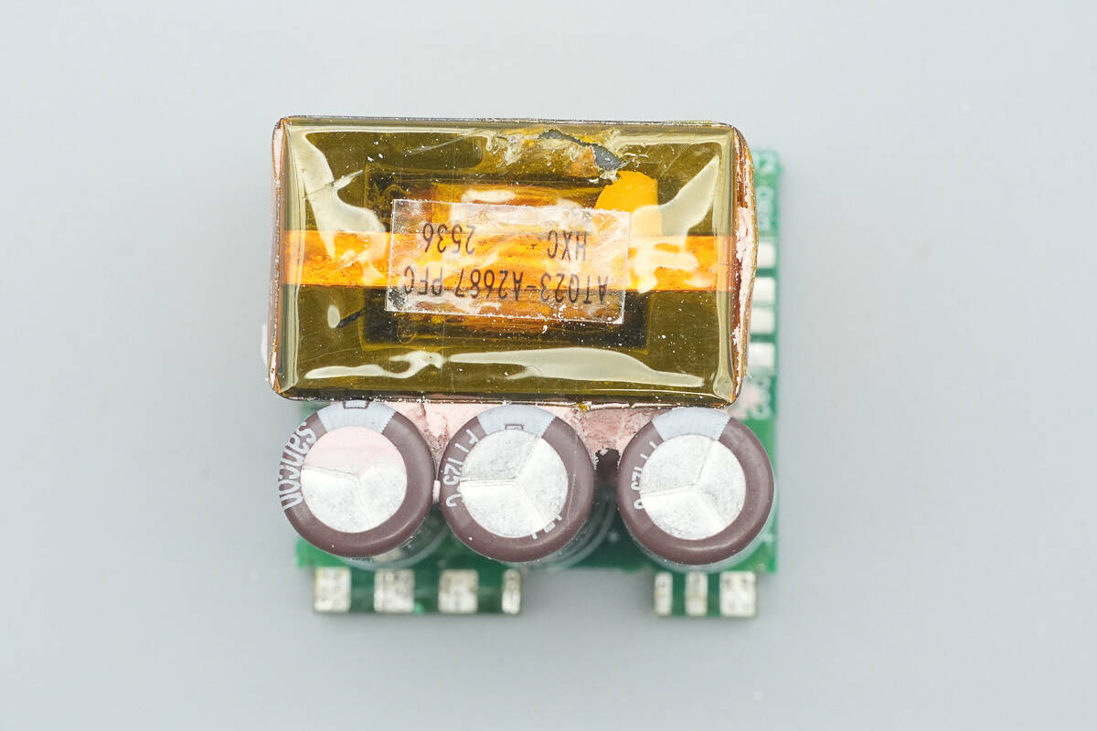
After removing the three small PCBs in the central area, the front of the support small PCB is found to house a transformer.
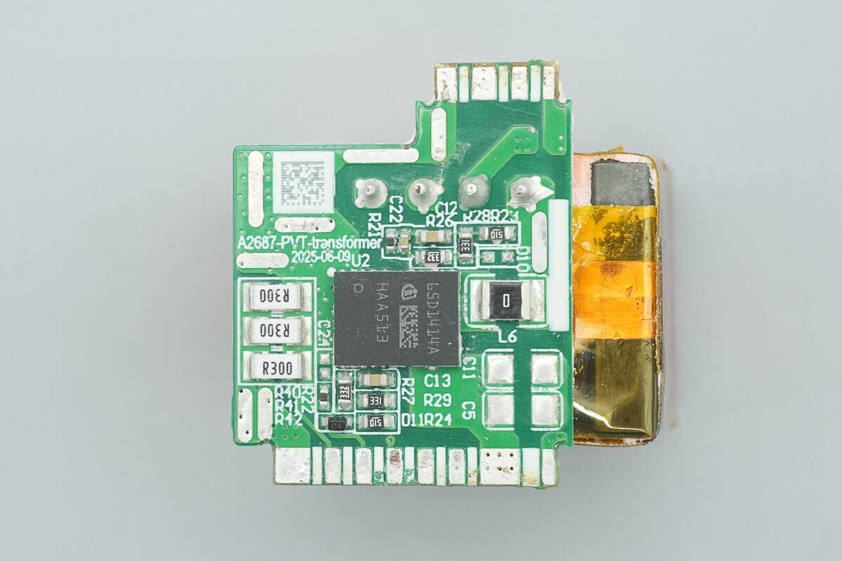
On the back side, there is a primary MOSFET.
The top small PCB houses a film capacitor and a solid capacitor.
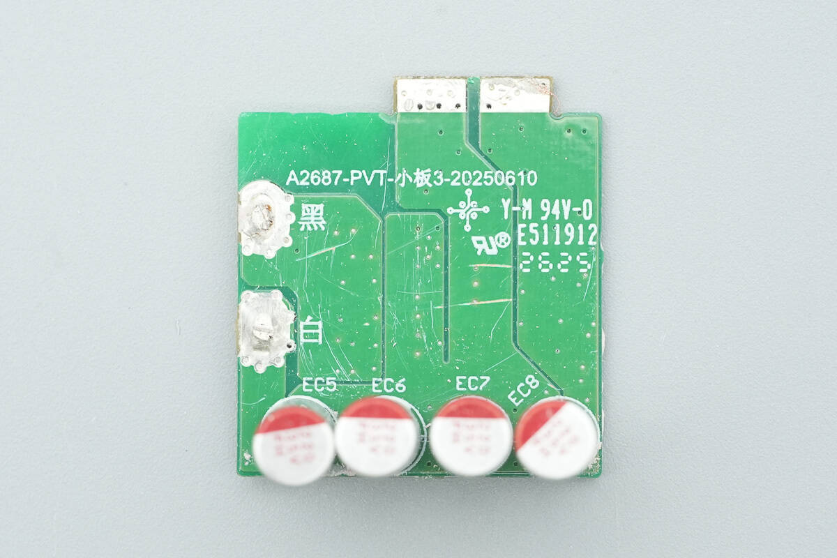
The front of the synchronous rectification small PCB is equipped with four solid capacitors.
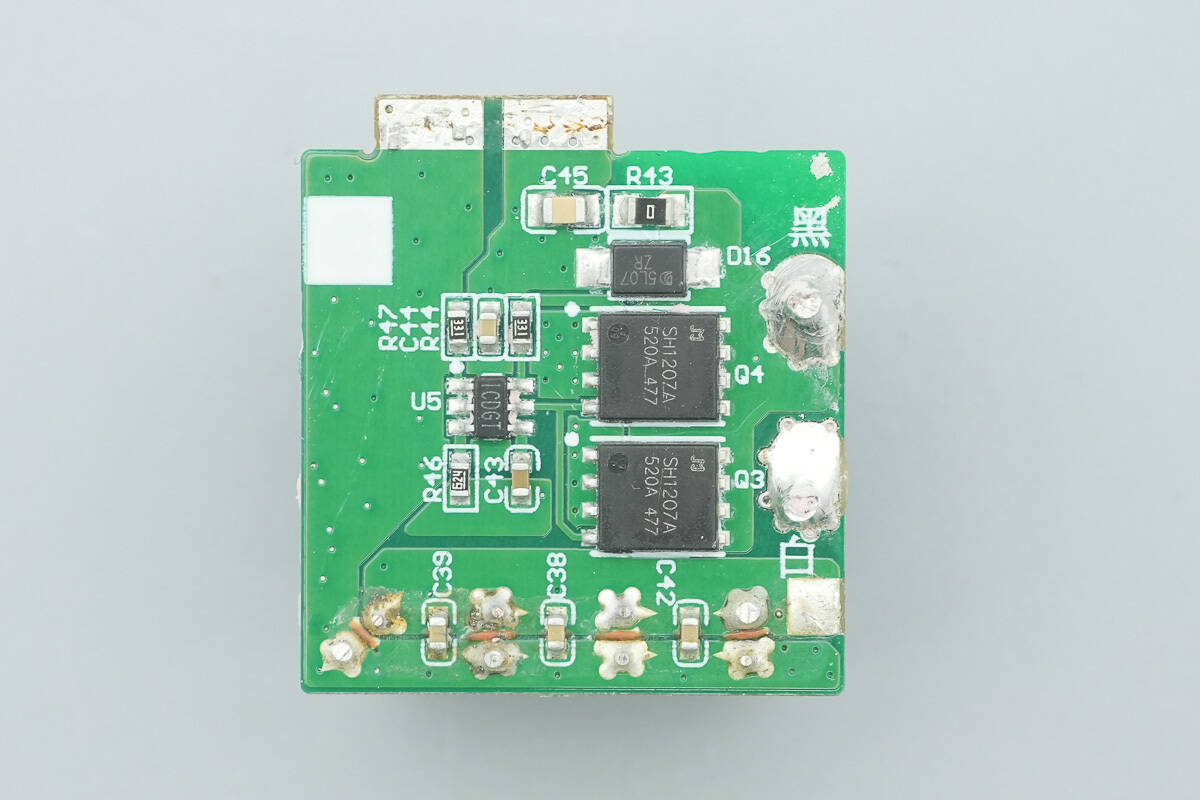
On the back side, there is a synchronous rectifier controller along with the synchronous rectifiers.
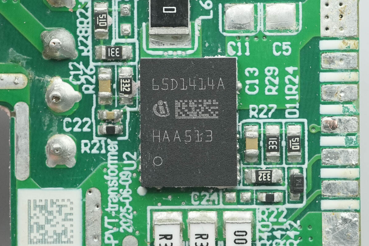
The GaN half-bridge chip is from Infineon, model IGI65D1414A3MS. The chip integrates a half-bridge power stage consisting of two enhancement-mode GaN transistors, each with a typical on-resistance of 140 mΩ and a voltage rating of 650 V, packaged in a compact 6×8 mm QFN‑32.
The resonant capacitor is from DGCX, rated at 0.47 µF, 250 V.
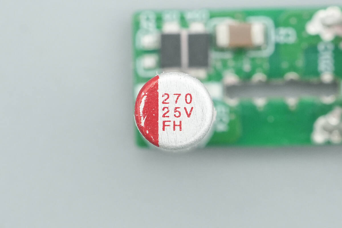
The capacitor supplying power to the master control chip is rated at 25 V, 270 µF.
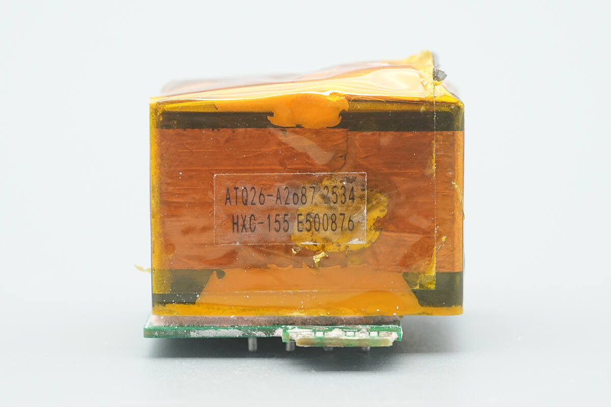
The transformer uses an ATQ26 magnetic core.

The 1018 optocoupler is from QUNXIN and is used for output voltage feedback.
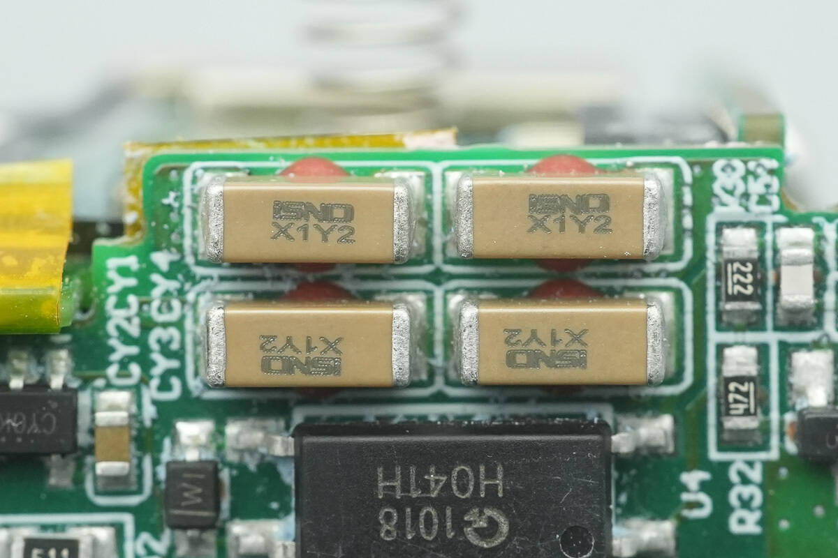
The four SMD Y capacitors are from ISND, connected in pairs in series to enhance the safety rating.
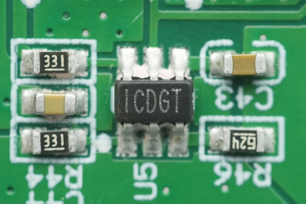
The synchronous rectifier controller is from MPS, marked ICDGT, and comes in a SOT23‑6 package.
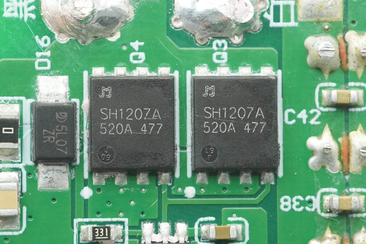
The synchronous rectifiers are from JJWD, model JMSH1207AG, rated 120 V with an on-resistance of 5.6 mΩ, housed in a DFN 5×6 mm package.
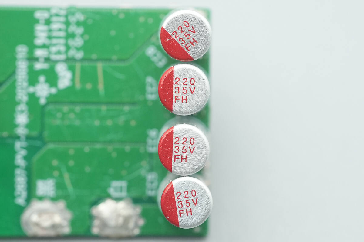
The four solid capacitors for output filtering are all rated at 35 V, 220 µF.
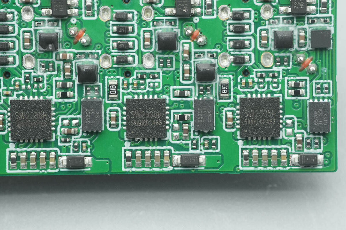
All three USB-C ports use the same output control scheme, so only one set will be described.
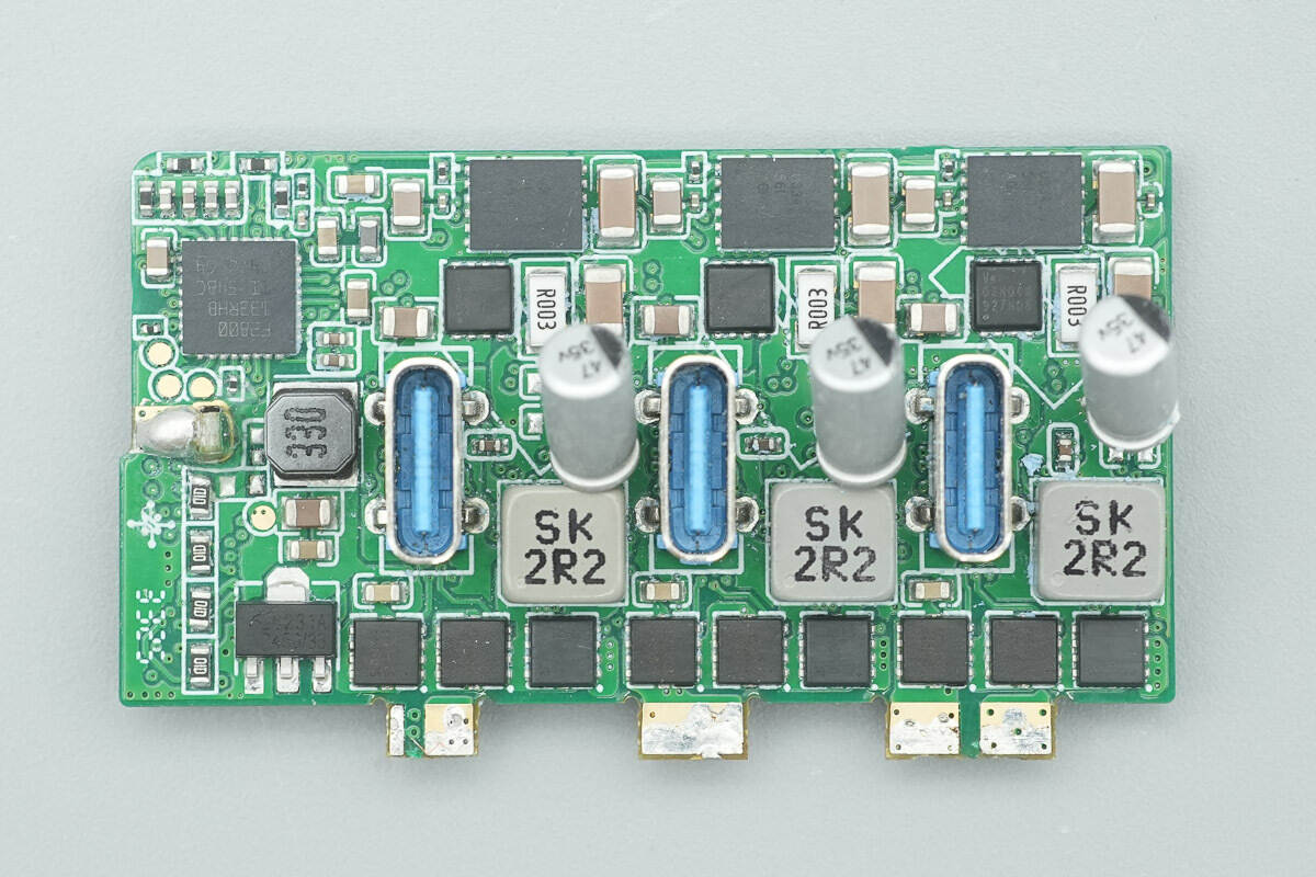
The front of the small PCB houses the MCUs, synchronous buck MOSFETs, buck inductors, solid capacitors, VBUS MOSFETs, and isolated power modules, among other components.
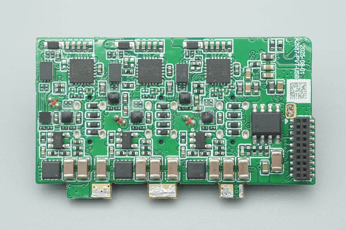
The back side houses synchronous buck converters, synchronous buck MOSFETs, digital isolators, protocol chips, and other components.
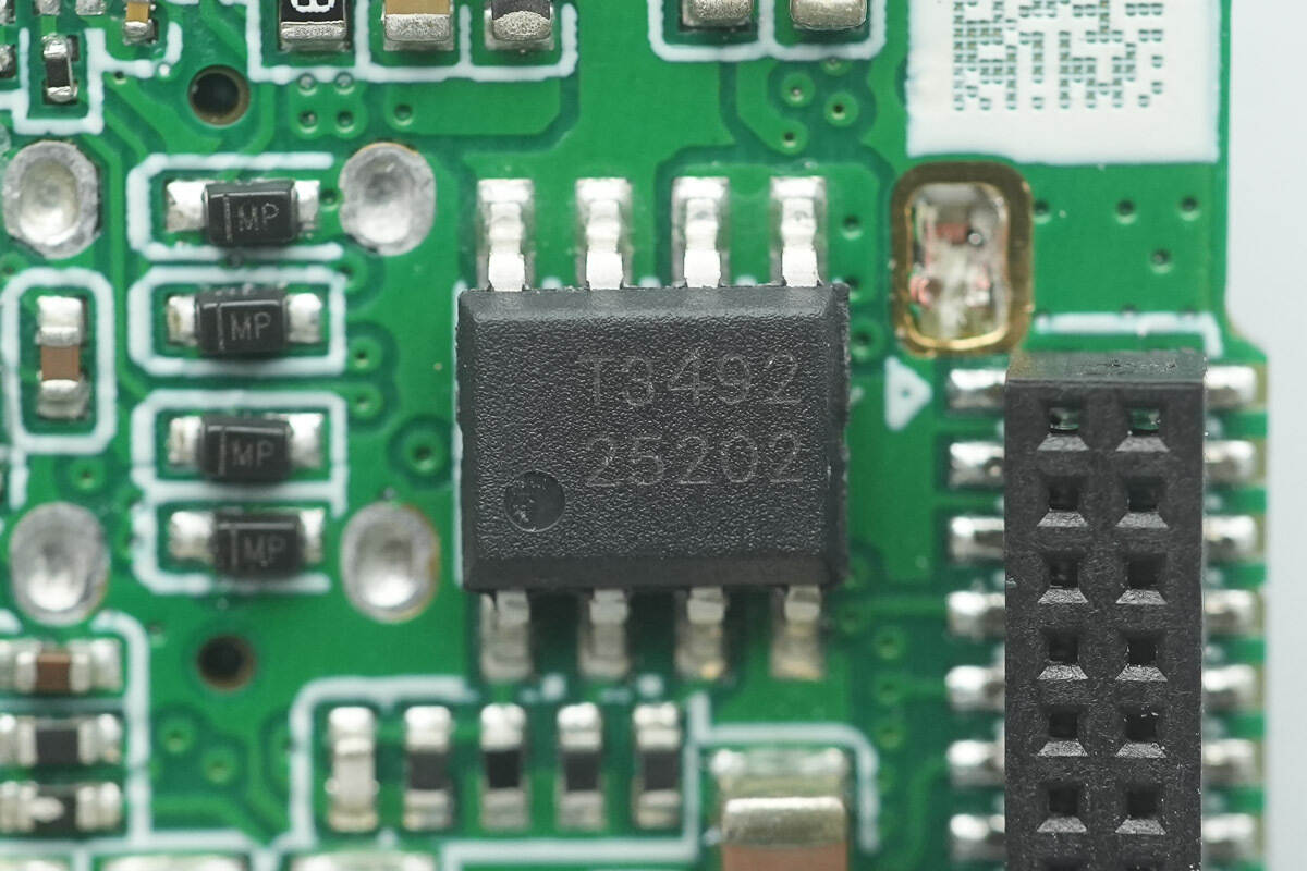
The synchronous buck converter is from Tollsemi, model TMI3492. It is a wide-input, high-efficiency 2 A synchronous rectified buck converter that integrates a 120 mΩ high-side power MOSFET and a 50 mΩ low-side power MOSFET, capable of delivering up to 2 A total output current at 5 V output.
The TMI3492 features advanced production-grade protection functions, including undervoltage lockout, thermal shutdown, soft start, and input overvoltage protection, and comes in an SOP8 package.
Close-up of the accompanying buck inductor.
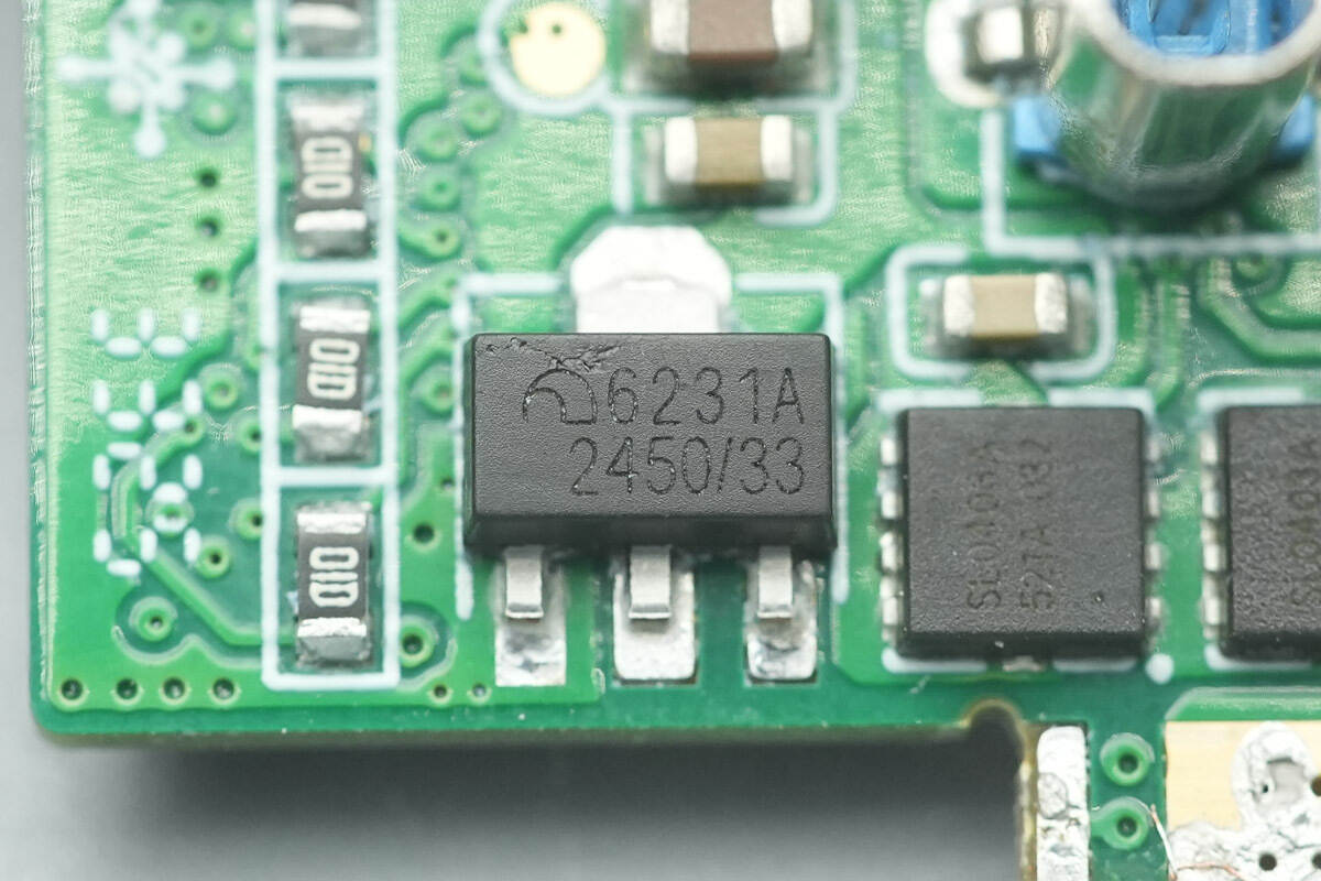
A voltage regulator chip marked 6231A is from Microne.
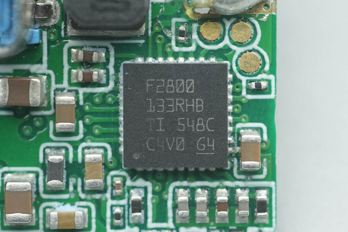
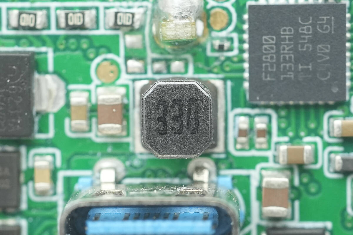
The TMS320F2800133RHB is a real-time microcontroller from TI’s C2000™ series. It features a 32-bit C28x DSP core with a maximum clock frequency of 120 MHz, 14 ePWM channels (including 2 channels with 150 ps high-resolution capability), high-speed ADCs, hardware protection comparators, and a rich set of communication interfaces. It is designed for high-precision, high-dynamic-response digital control applications and comes in a VQFN32 package.
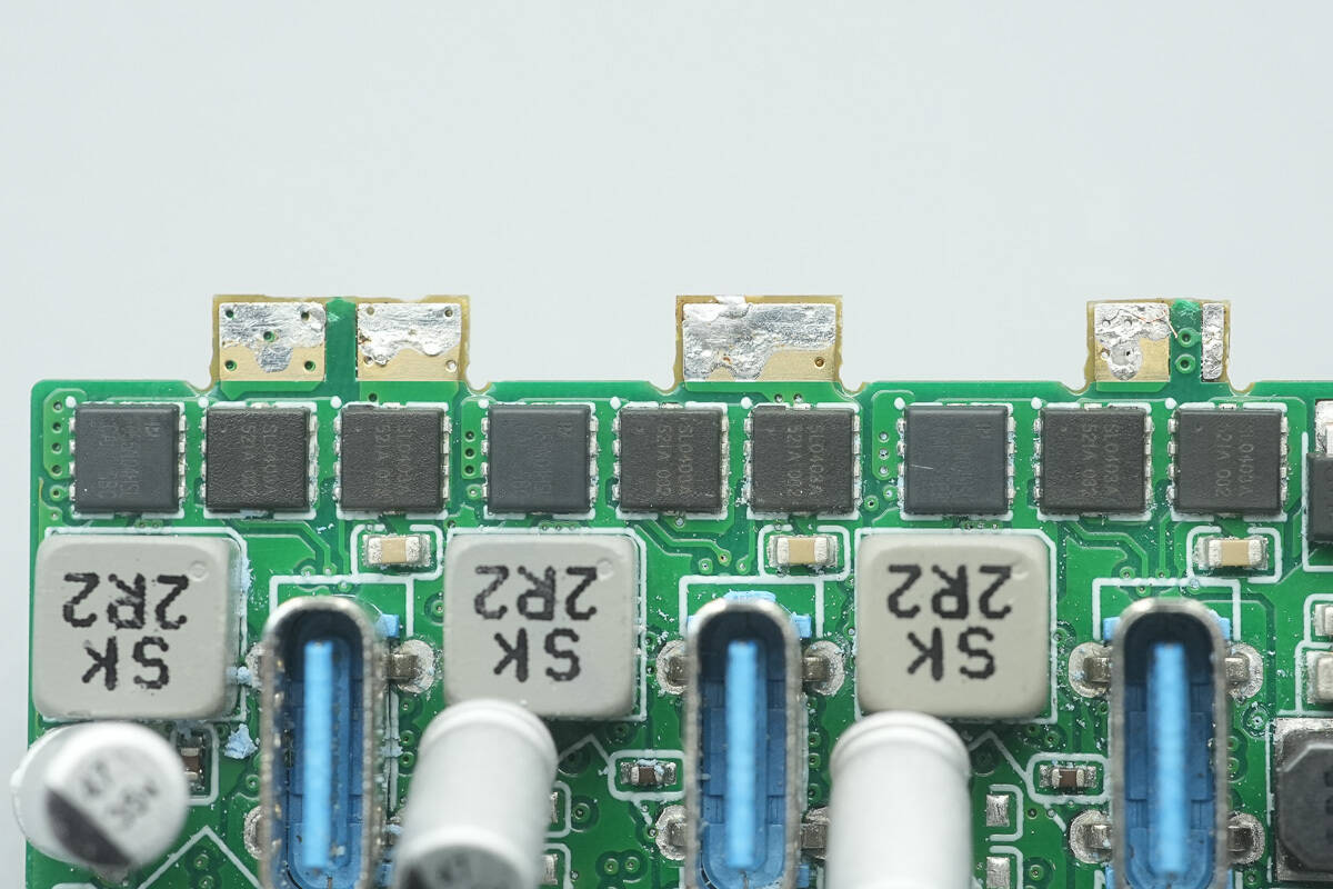
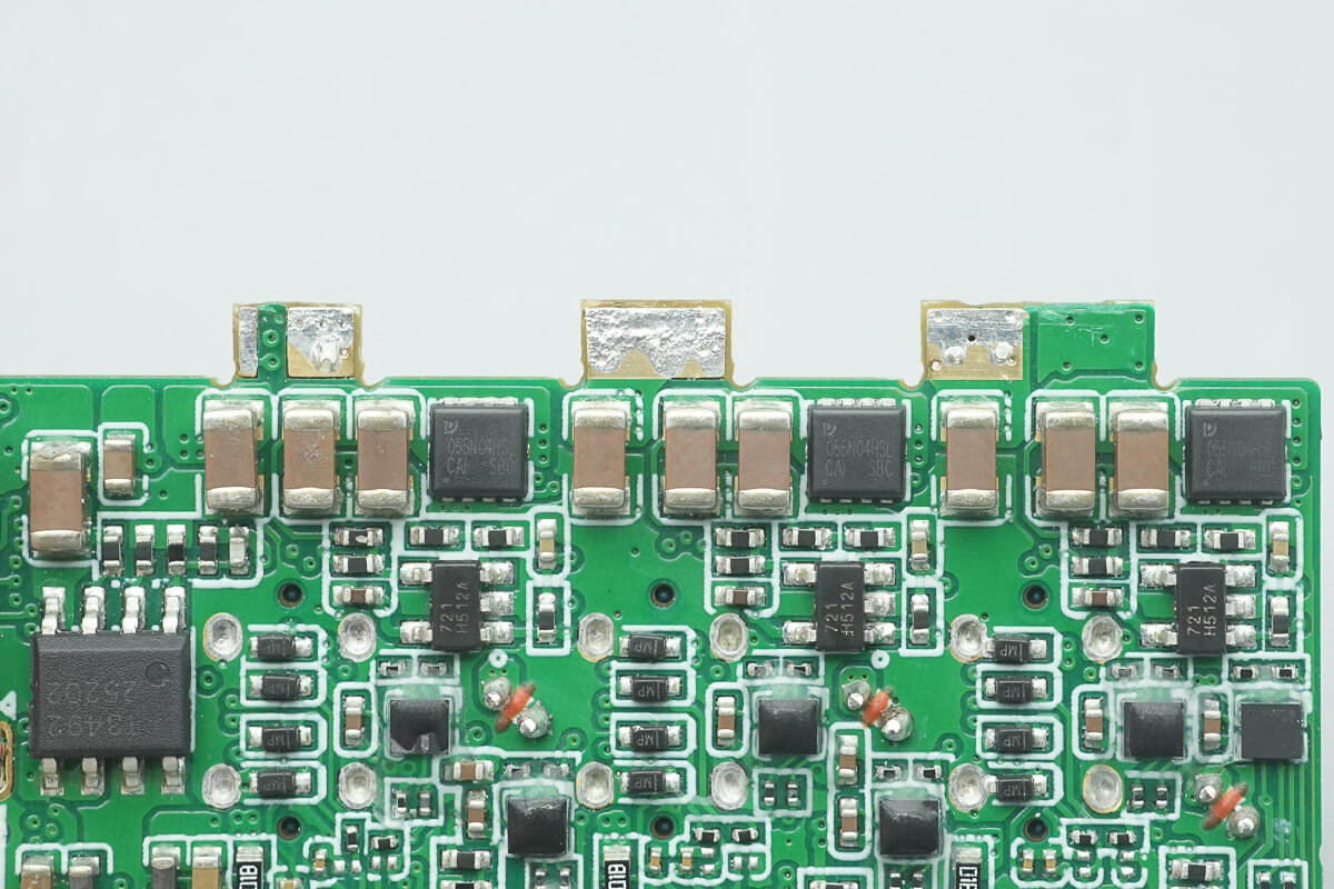
There are three sets of synchronous buck MOSFETs, totaling 12 units. Each set consists of two JJWD JMSL0403AU MOSFETs paired with two PY MOSFETs marked 055N04HSL.
The other three PY MOSFETs are located on the back side of the small PCB.
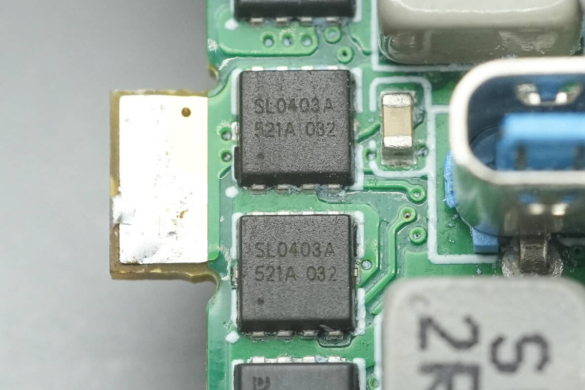
The JJWD JMSL0403AU is an N‑MOSFET with a voltage rating of 40 V and an on-resistance of 2.5 mΩ, housed in a PDFN 3×3‑8L package.
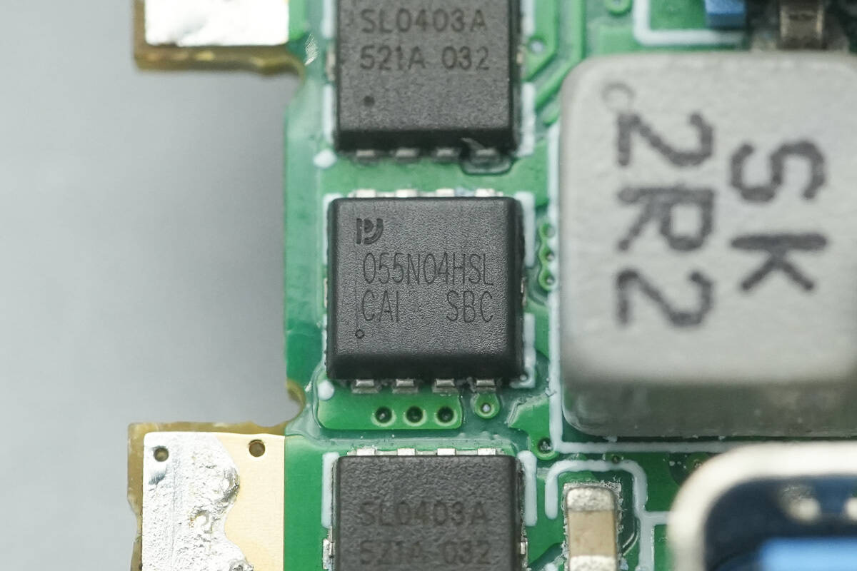
The PY MOSFET is marked 055N04HSL.
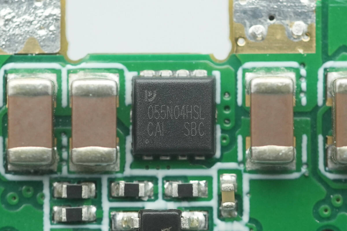
Close-up of the PY MOSFETs on the back side.
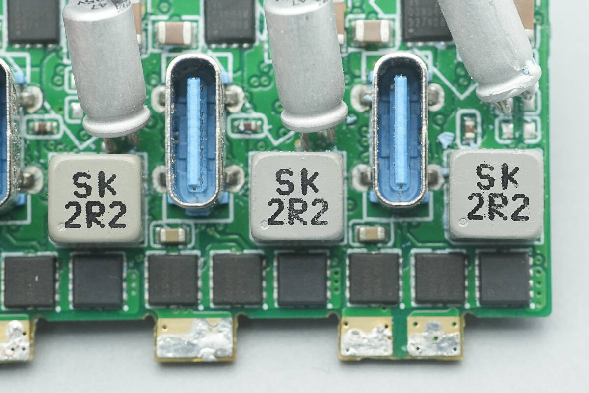
Close-up of the three 2.2 µH buck inductors. They measure just 5.5×5.5 mm, much smaller than conventional inductors. This, combined with Anker's proprietary architecture, significantly reduces the PCB area occupied by the DC-DC circuit.
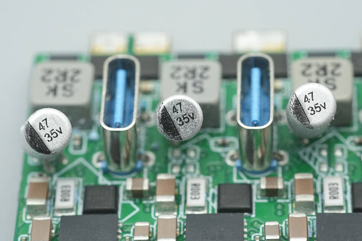
The three solid capacitors for output filtering are all rated at 35 V, 47 µF.

It is equipped with isolated power modules and VBUS MOSFETs for each port's output.
The corresponding area on the back side houses the isolators and protocol chips.
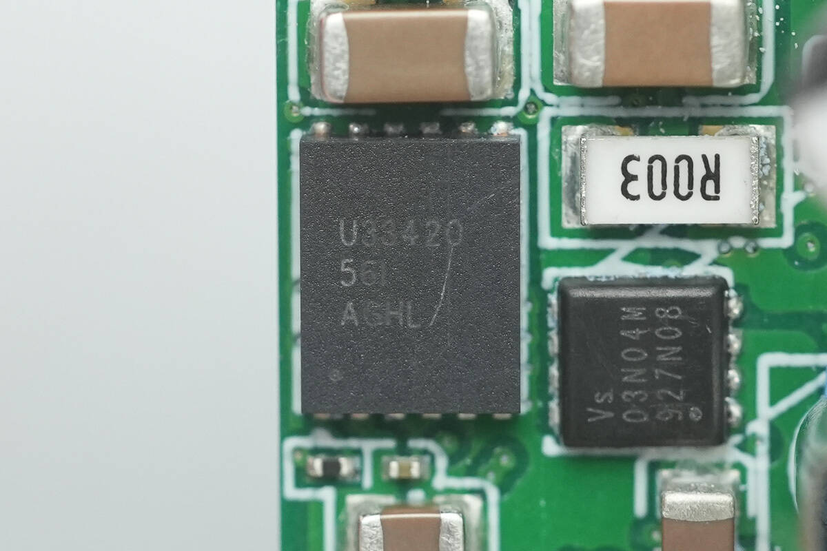
The isolated power modules are TI UCC33420. This is an ultra-compact, high-efficiency, industrial-grade isolated DC/DC power module that supports a 3kVRMS isolation rating and 6.5kVPK surge withstand capability, meeting several international safety certification requirements. The module uses integrated transformer technology to deliver up to 1.5W of output power in a tiny 4×5 mm VSON package, with excellent heat dissipation and layout adaptability.
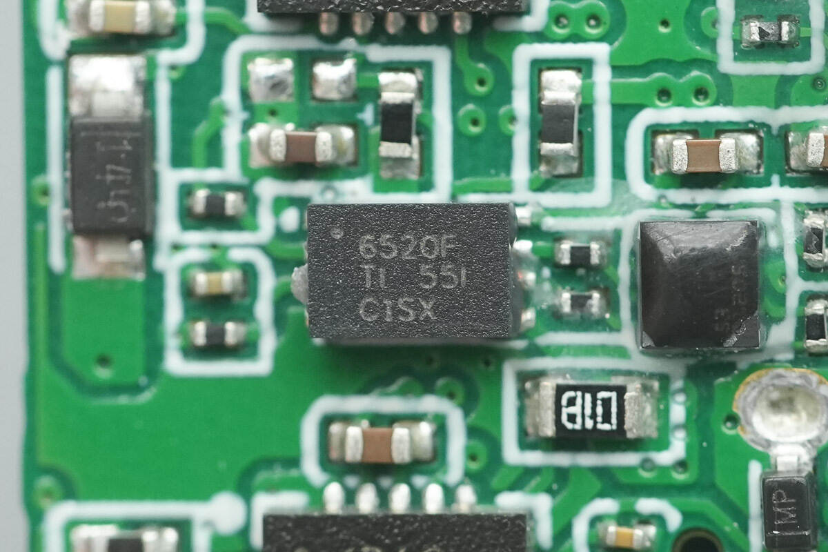
The three digital isolators are TI ISO6520. This is a high-performance, dual-channel functional isolator designed for cost-sensitive, space-constrained applications that require isolation from non-safety applications. While isolating CMOS or LVCMOS digital I/O, the device offers high electromagnetic immunity, low emissions, and low power consumption.
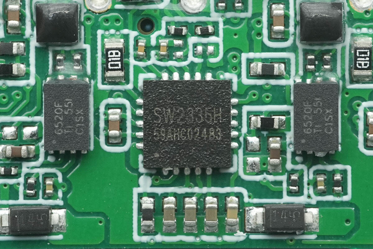
The protocol chips for all three ports are iSmartWare SW2335H. This is a highly integrated fast-charging protocol controller, featuring an ARM Cortex-M0 core with a maximum operating frequency of 40 MHz, and supporting common peripheral interfaces such as I2C, UART, and GPIO.
The SW2335H integrates Type-C interface logic and PD3.1 PHY, supporting PD3.1, BC1.2, UFCS, and various mainstream DPDM fast charging protocols, with a maximum output voltage of 32V. It is primarily used in applications such as adapters, power strips, and car chargers.
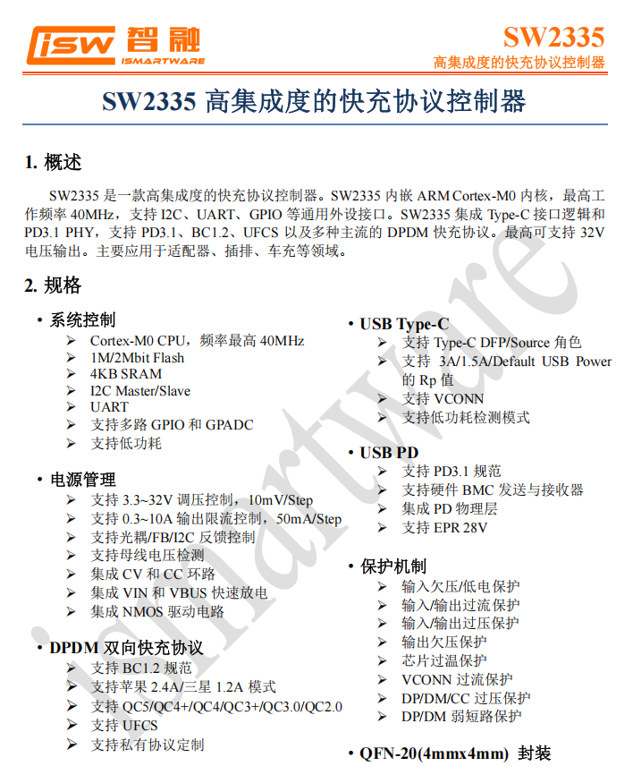
Here is the information about iSmartWare SW2335H.
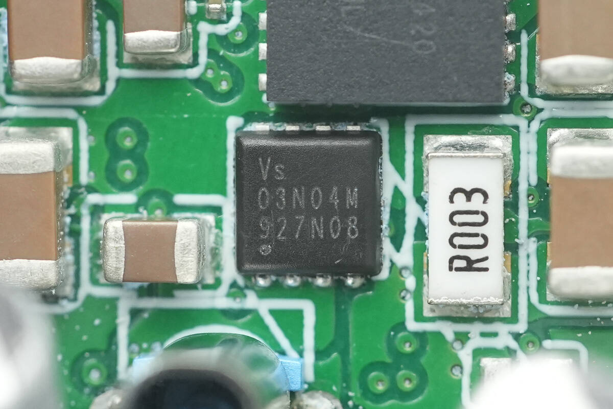
The three VBUS output MOSFETs are Vergiga VSE003N04MSC-G, N‑MOSFETs with a voltage rating of 40 V and an on-resistance of 2.3 mΩ, packaged in a PDFN 3333 package.
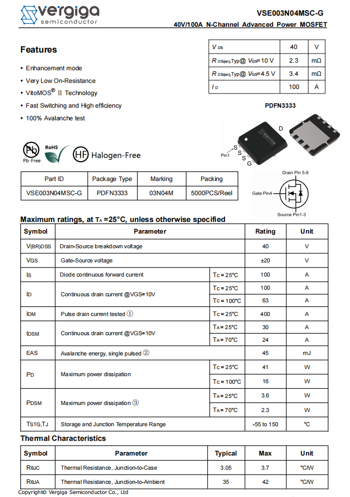
Here is the information about Vergiga VSE003N04MSC-G.
Close-up of the three USB-C sockets.
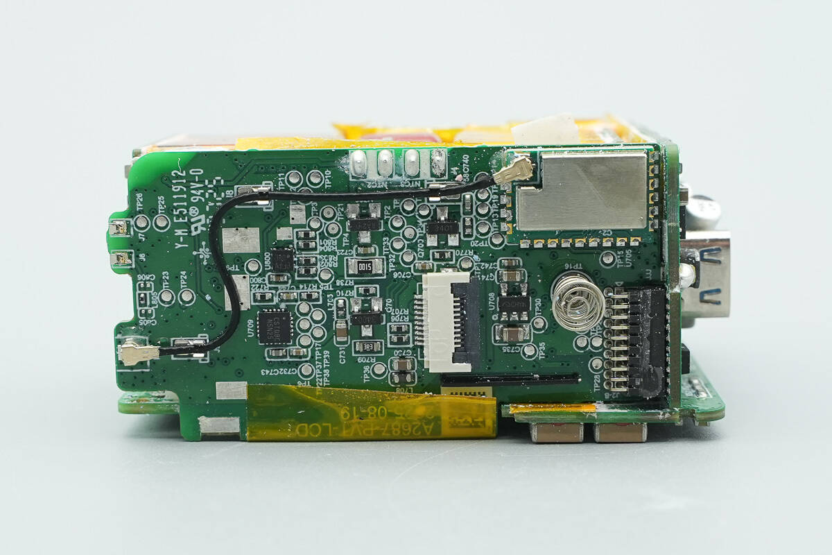
The front of the screen PCB features a touch controller chip, a wireless communication module, and other components.
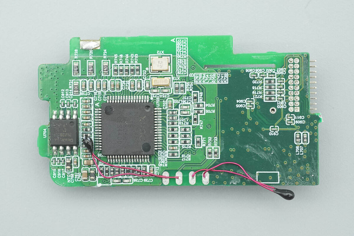
The other side of the screen PCB houses the MCU, memory, surface-mount crystals, and other components.
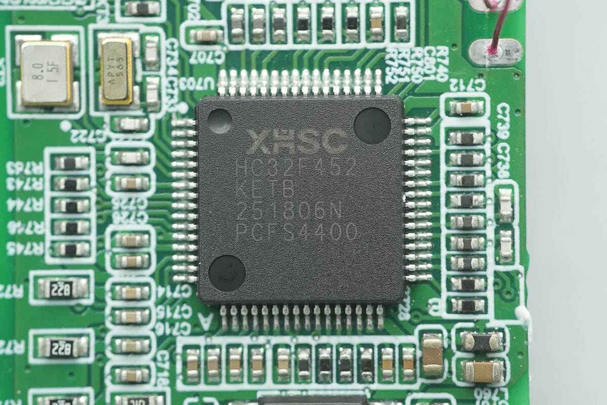
The MCU is from XHSC, model HC32F452KETB-LQFP64. The HC32F45x series features a high-performance 32-bit ARM Cortex-M4 core with a maximum operating frequency of 200 MHz. Additionally, it integrates high-speed on-chip memory and a rich set of peripheral functions, supporting a wide voltage range (1.8–3.6V), a wide temperature range (-40 to 105°C), and various low-power modes.
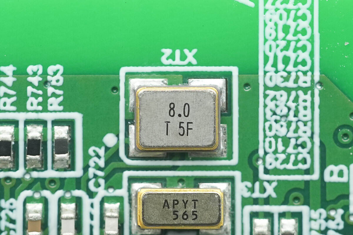
Close-up of the external 8.0 MHz surface-mount crystal oscillator.
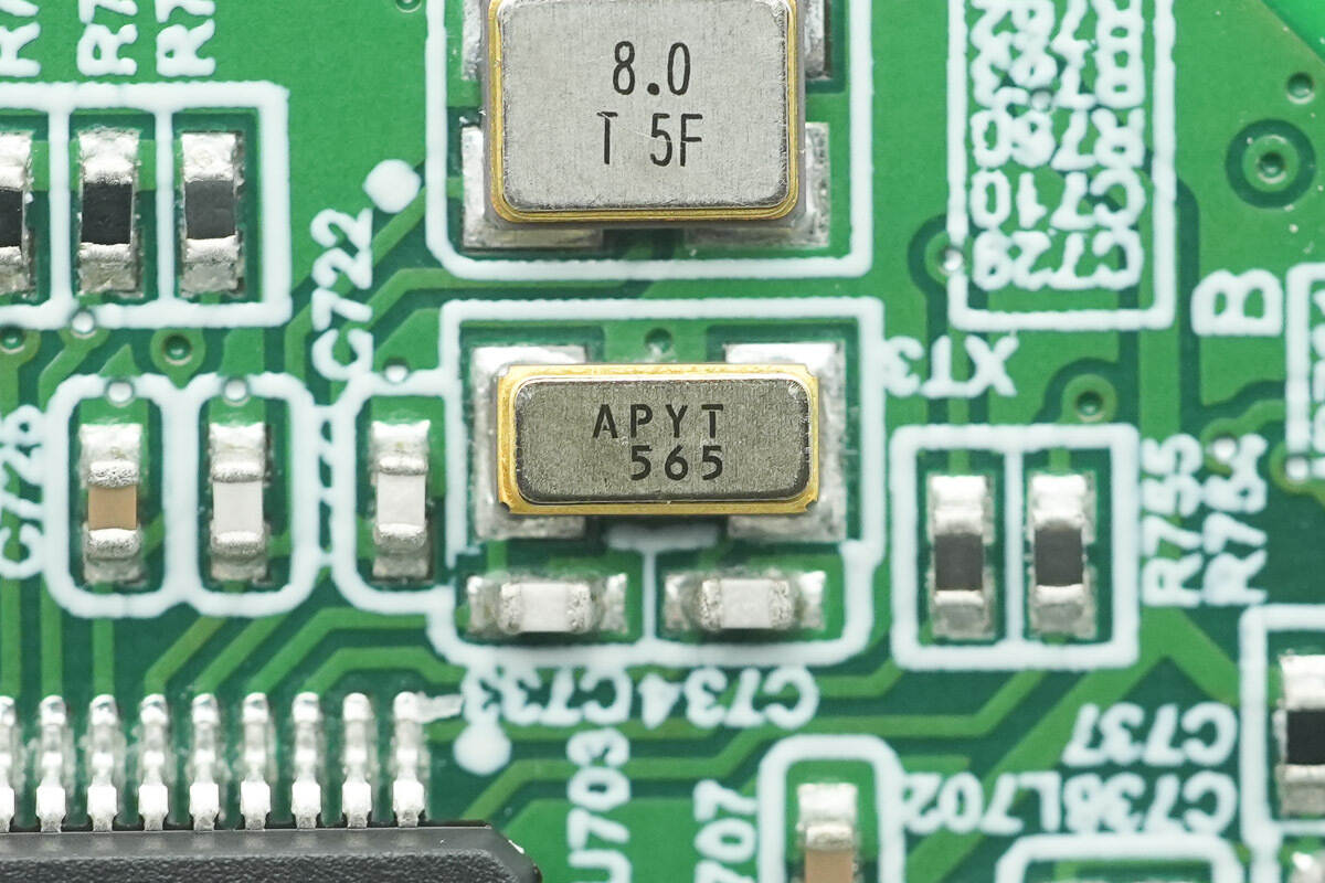
Close-up of the 32.768 kHz surface-mount crystal oscillator.
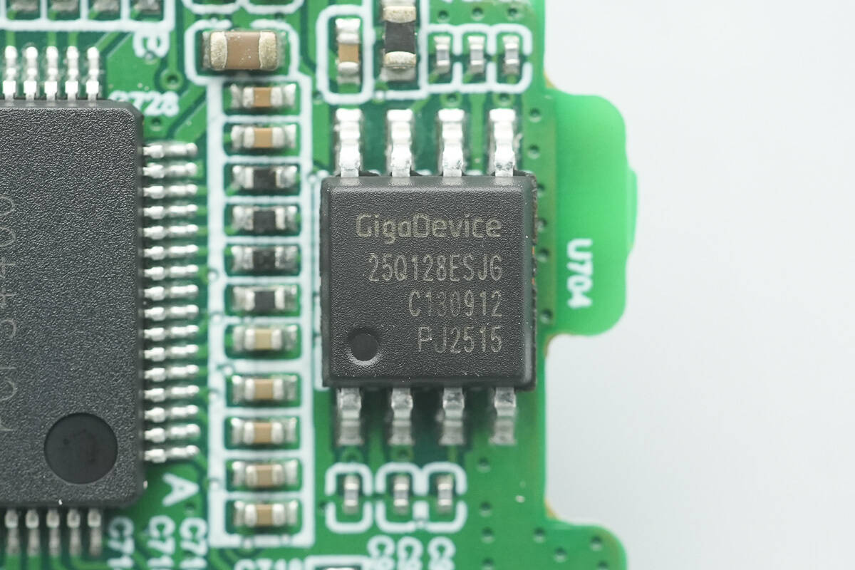
The memory is from GigaDevice, model GD25Q128E, with a capacity of 16MB. It supports a single-supply voltage range of 2.7–3.6V and comes in an SOP8 package.
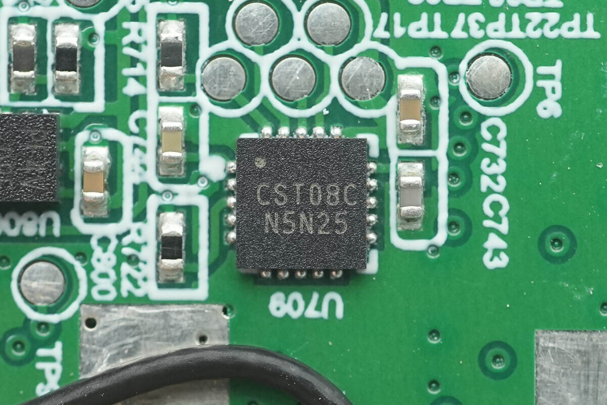
The HYNITRON CST08C is a high-performance self-capacitance touch chip. It uses a high-speed MCU core with an embedded DSP circuit, combined with fast self-capacitance sensing technology. The chip supports a variety of self-capacitance patterns, including triangles, and supports single-point gestures and real two-point operations, offering extremely high sensitivity and low standby power consumption. It comes in a QFN 3×3-20L package.
The Bluetooth SoC is from BLUETRUM, model AB2026B3. This is a low-power, high-performance Bluetooth Low Energy (BLE) System-on-Chip (SoC) designed specifically for IoT and disposable devices. It features a 32-bit RISC-V processor core with a clock frequency of up to 120 MHz. The SoC is equipped with 72KB of RAM and NOR flash memory, and integrates a high-performance 2.4GHz RF transceiver, ensuring stable and efficient Bluetooth wireless connectivity.
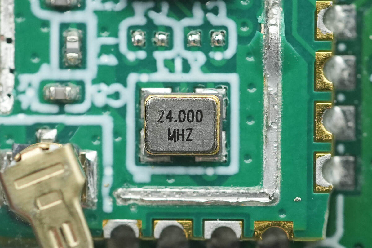
Close-up of the 24.000 MHz crystal oscillator.
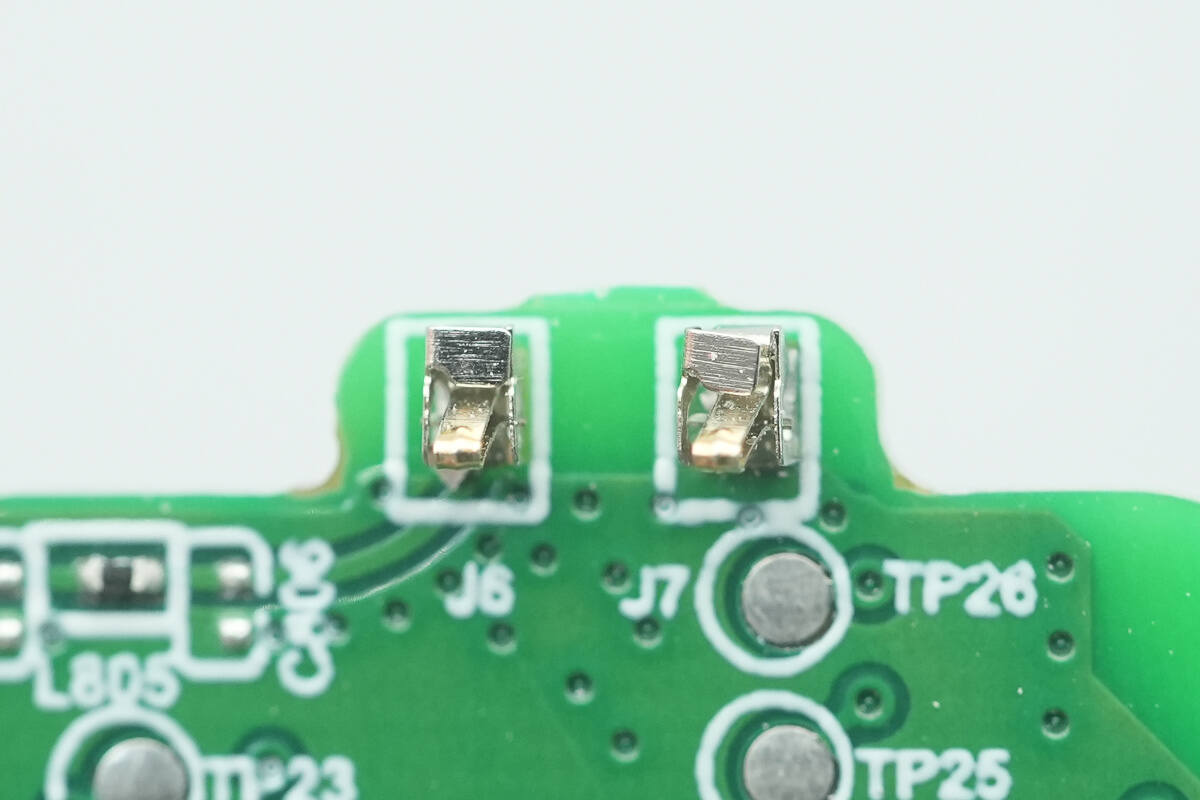
Close-up of the contact points used to connect the Bluetooth antenna.
Close-up of the two thermistors.
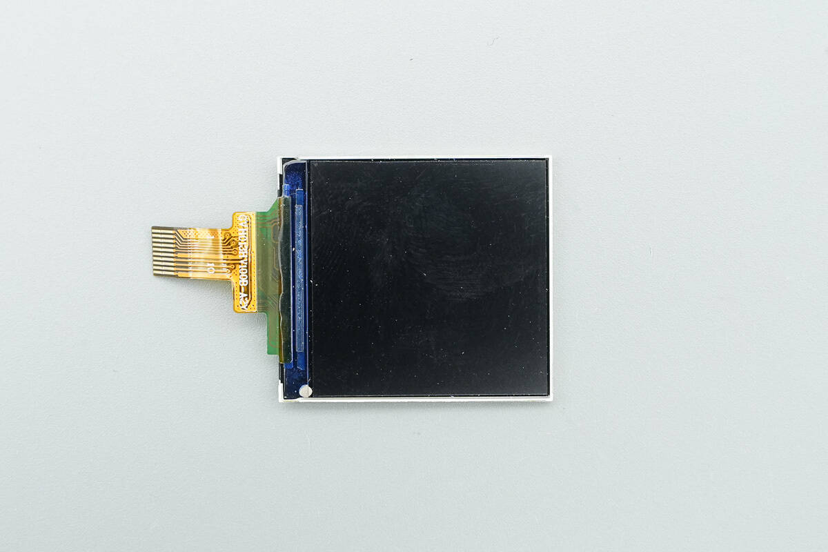
Close-up of the screen.
Well, those are all components of the Anker Prime 160W Charger with Smart Display.
Summary of ChargerLAB
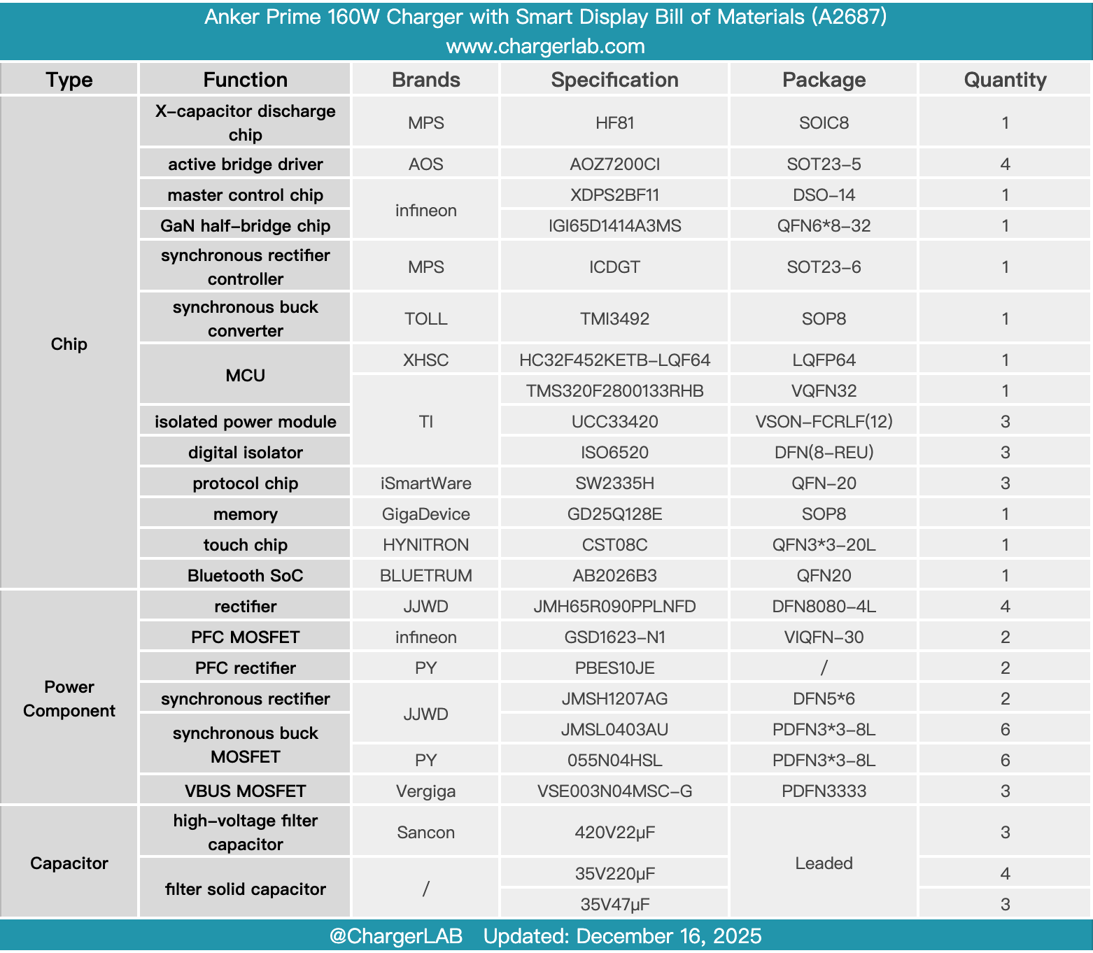
Here is the component list of the Anker Prime 160W Charger with Smart Display for your convenience.
The 3D waistline design on both sides of the body enhances the insertion and removal experience. The matte rubber coating on the prongs ensures stability. The screen and buttons are integrated into a single panel, providing an immersive and tactile user interaction experience.
It is equipped with three USB-C ports that support multiple protocols, including PD3.1, QC3.0, PPS, and SCP. It provides up to 140W for a single port and a total power of 160W. Additionally, it supports smart and customizable power distribution, ensuring broad compatibility with various brand devices for efficient fast charging.
The smart display not only shows total power, individual port power, temperature, and other data, but also provides the cable specification details. It also supports 360° gravity-sensing automatic rotation. The charger can connect to the app for further personalized settings and continuous OTA updates. Its size is extremely compact, maximizing portability.
After taking it apart, we found that it uses a PFC+HFB efficient topology design. The controllers and GaN devices are from manufacturers like Infineon and MPS. The core components of the output isolation circuit are from TI. The protocol chips for all three ports are iSmartWare SW2335H.
The module features an extremely compact stacked design, with a very tight component layout. It is heavily filled with thermal adhesive and covered with thermal pads to assist with heat dissipation. Additionally, adequate insulation and isolation have been applied between components to ensure safety during long-term use.
Related Articles:
1. Teardown of Anker Nano 75W Car Charger (A2738)
2. Teardown of DJI Power 1000 Mini Power Station (DYM1000M)
3. Teardown of Honor Choice LCHSE Clip-On Earphone 2 Pro