Introduction
ChargerLAB has completed a teardown of the WEX 65W charger, which utilizes SiC power devices to achieve high power density in a compact 2 USB-C and a USB-A multi-port configuration.
It features a foldable pin design and a minimalist, square-profile chassis available in black and gray. The 2 USB-C and a USB-A interface, each equipped with an orange plastic sheet to support high-speed charging for mobile devices, tablets, and ultrabooks.
Let’s dive into the internals. We’ll perform a full teardown to see if the engineering and build quality match the premium exterior.
Product Appearance
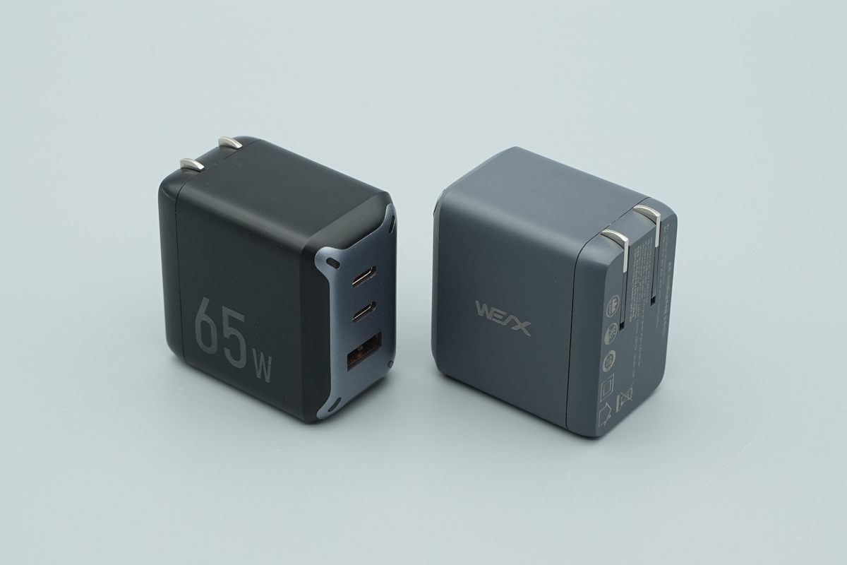
Available in classic black and gray, the WEX 65W charger maintains a minimalist, cubic design. Notably, the internal engineering and build quality remain consistent across both versions.
Focusing on the gray one, the fit and finish at the seam where the pin-side housing meets the main body is tight and remarkably well-built.
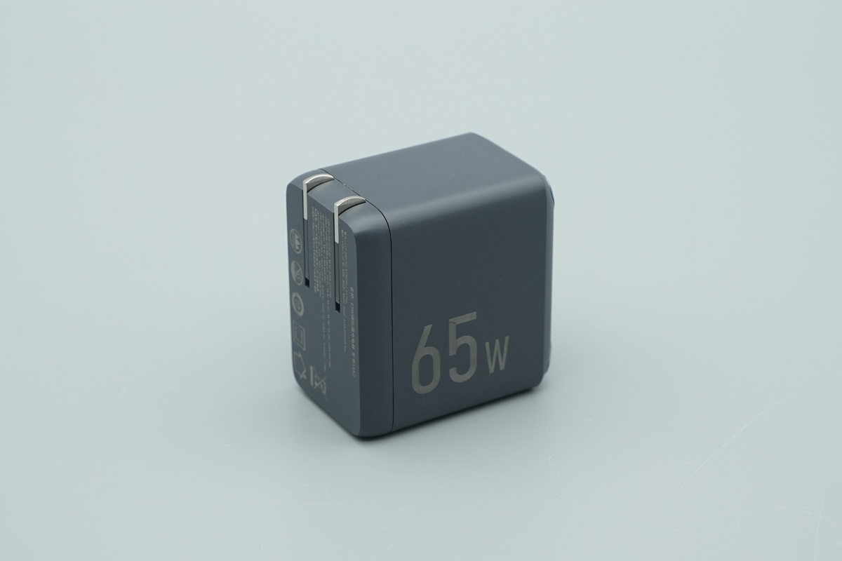
The side of the chassis features a prominent '65W' marking, clearly indicating the Max rated output power of the unit.
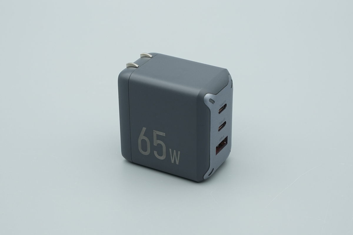
The output end features a silver-gray cover plate with chamfered edges, enhancing both industrial design and structural depth. It is equipped with a tri-port configuration: two USB-C ports and one USB-A port.
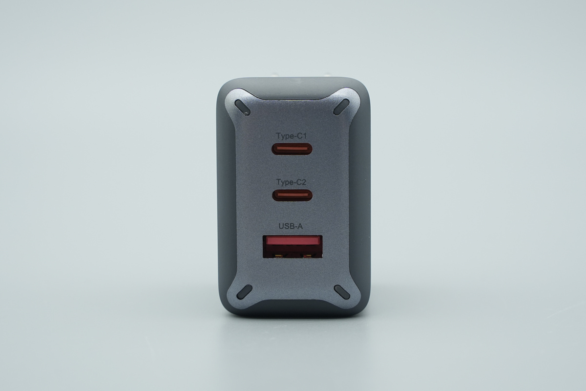
The output end features two USB-C ports (C1, C2) and one USB-A port. Each port is equipped with an orange plastic sheet, signaling support for high-speed fast-charging protocols.
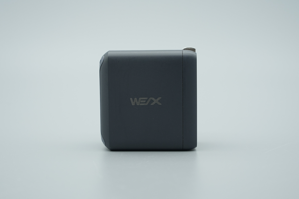
The WEX logo is prominently displayed on the side panel.
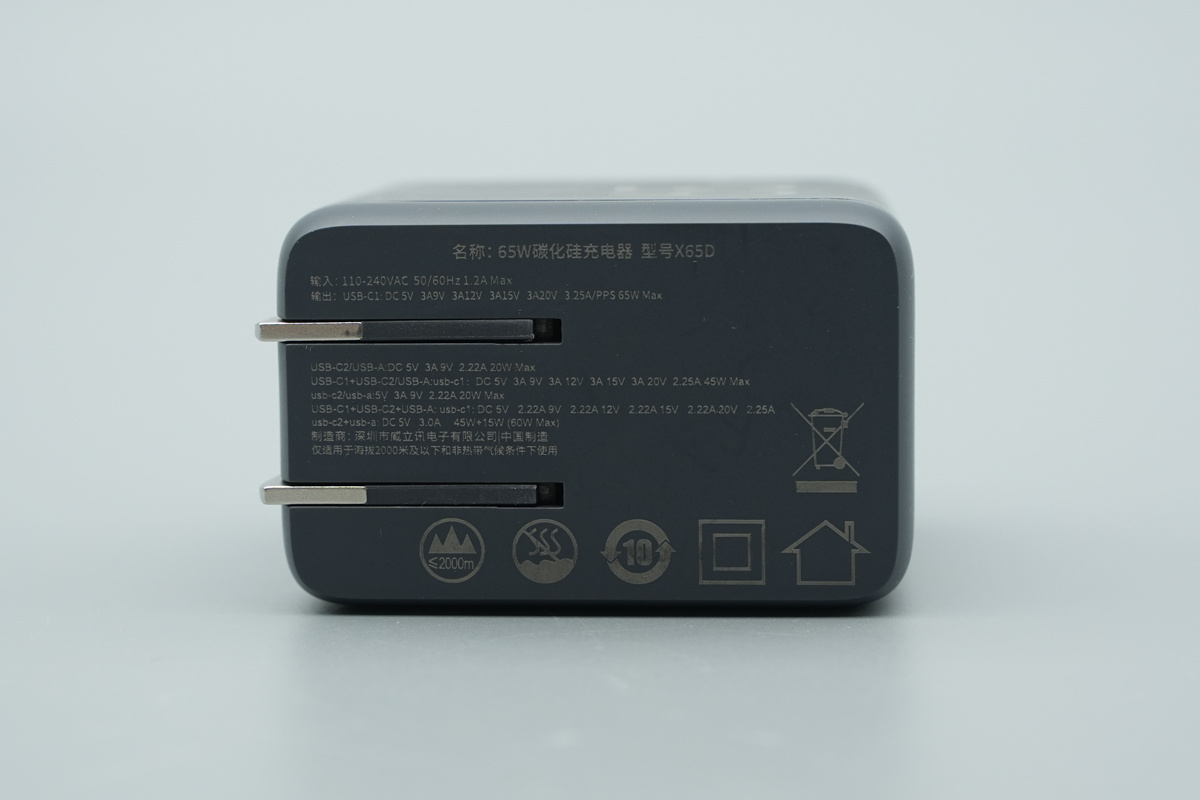
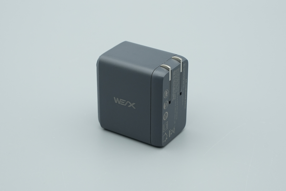
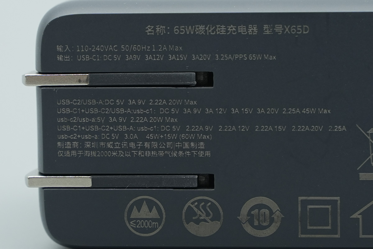
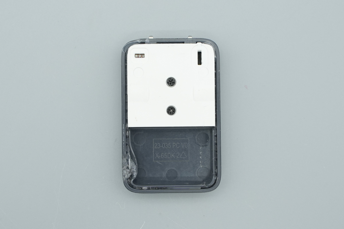
The base of it features a detailed technical specs label.
Product Specifications:
Name: the WEX 65W SiC Charger
Model: X65D
Input: 110-240V~ 50/60Hz 1.2A Max
Output:
USB-C1: 5V/3A, 9V/3A, 12V/3A, 15V/3A, 20V/3.25A (65W Max / PPS)
USB-C2 / USB-A: 5V/3A, 9V/2.22A (20W Max)
USB-C1+USB-C2/USB-A: USB-C1: 5V/3A, 9V/3A, 12V/3A, 15V/3A, 20V/2.25A (45W Max)
USB-C2/USB-A: 5V/3A, 9V/2.22A (20W Max)
USB-C1+USB-C2+USB-A: USB-C1: 5V/2.22A, 9V/2.22A, 12V/2.22A, 15V/2.22A, 20V/2.25A,
USB-C2+USB-A: 5V 3.0A, 45W+15W (60W Max)
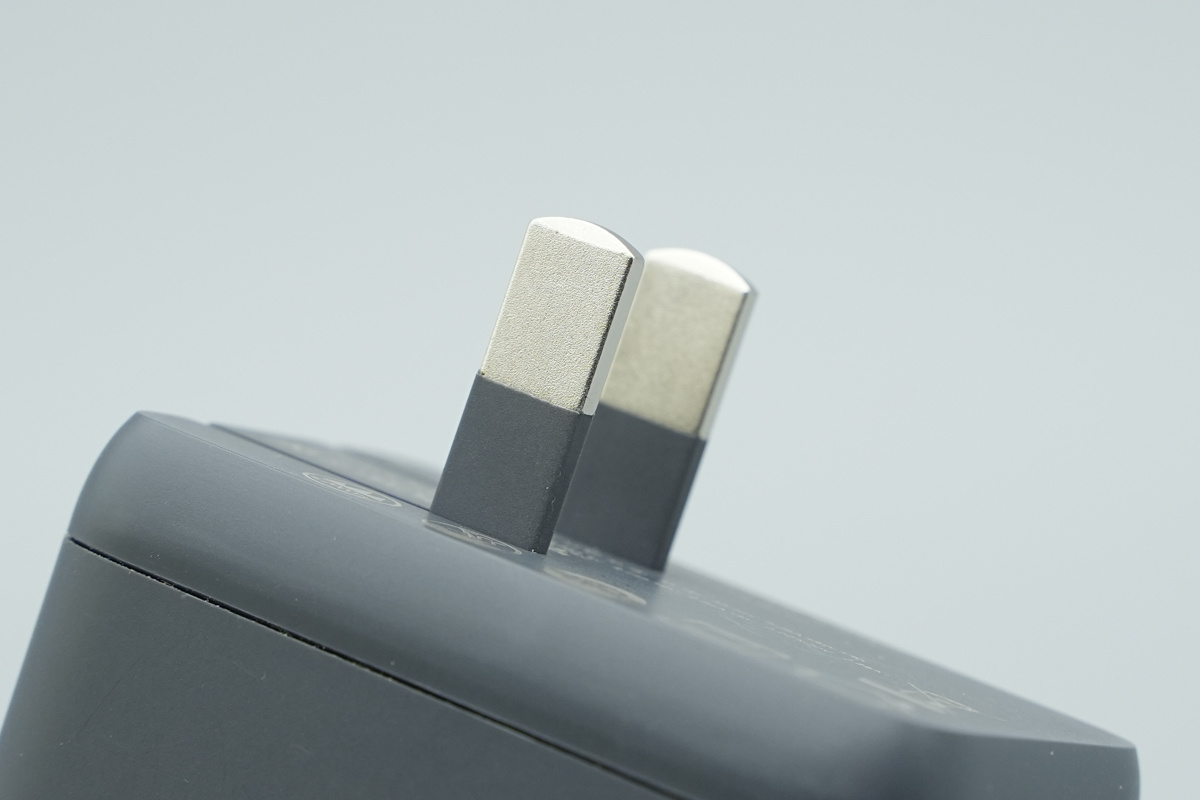
It is equipped with foldable AC pins compliant with Chinese standards, ensuring ease of storage and preventing accidental scratches to other items during transit
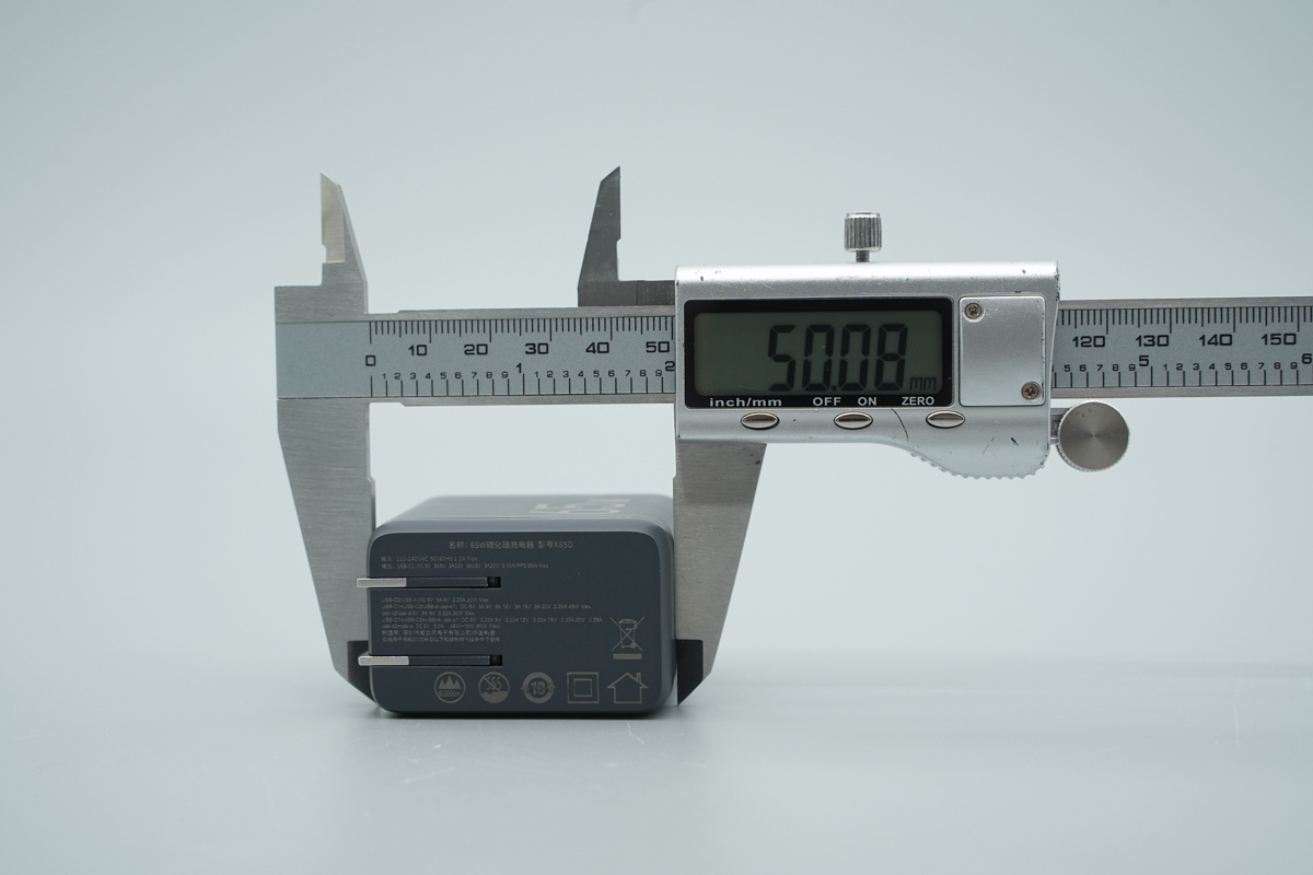
The length of the charger is about 50.08mm (1.972 inches).
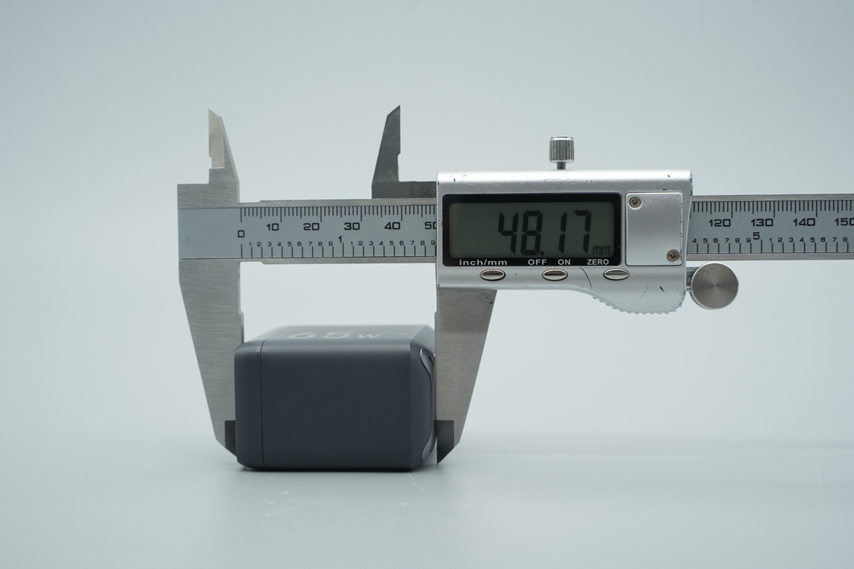
The width of the charger is about 48.17mm (1.897 inches).
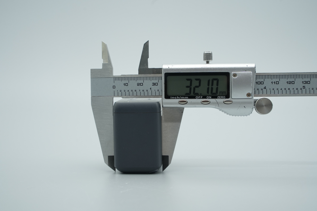
The thickness of the charger is about 32.10mm (1.264 inches).
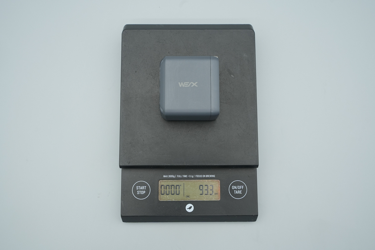
The weight is about 93.3g (3.29 oz).
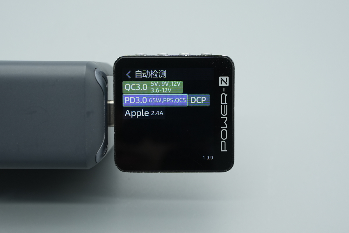
ChargerLAB POWER-Z KM003C shows that the USB-C1 port supports QC3.0, PD3.0/PPS, QC5, Apple 2.4A and DCP.
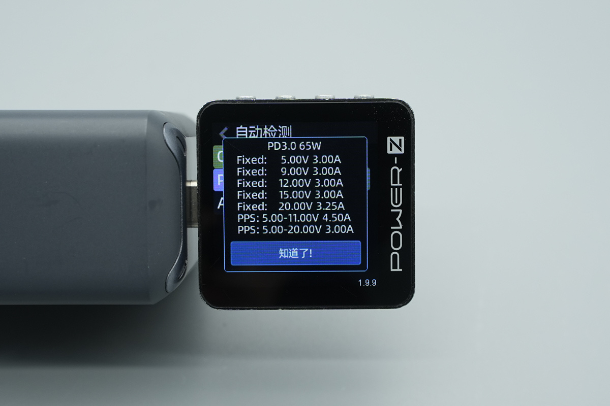
And it also supports four fixed PDOs of 5V3A, 9V3A, 12V3A, 15V3A and 20V3.25A, and features PPS subset: 5-11V4.5A and 5-20V3A.
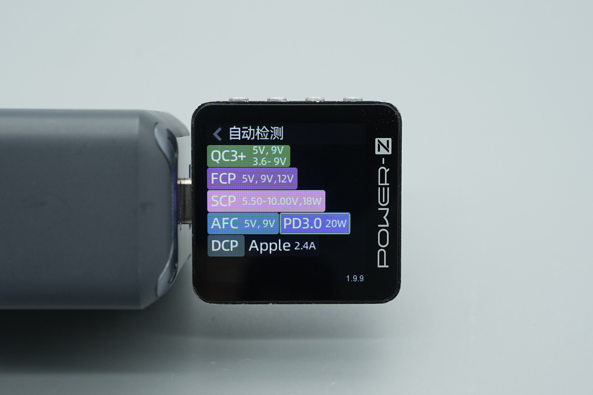
ChargerLAB POWER-Z KM003C shows that the USB-C2 port supports QC3+, FCP, SCP, AFC, PD3.0, Apple 2.4A and DCP.
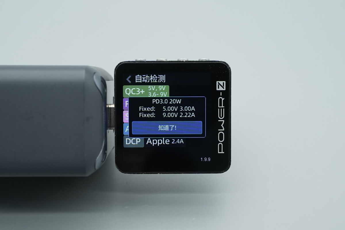
And it also supports four fixed PDOs of 5V3A and 9V2.22A, Max 20W.
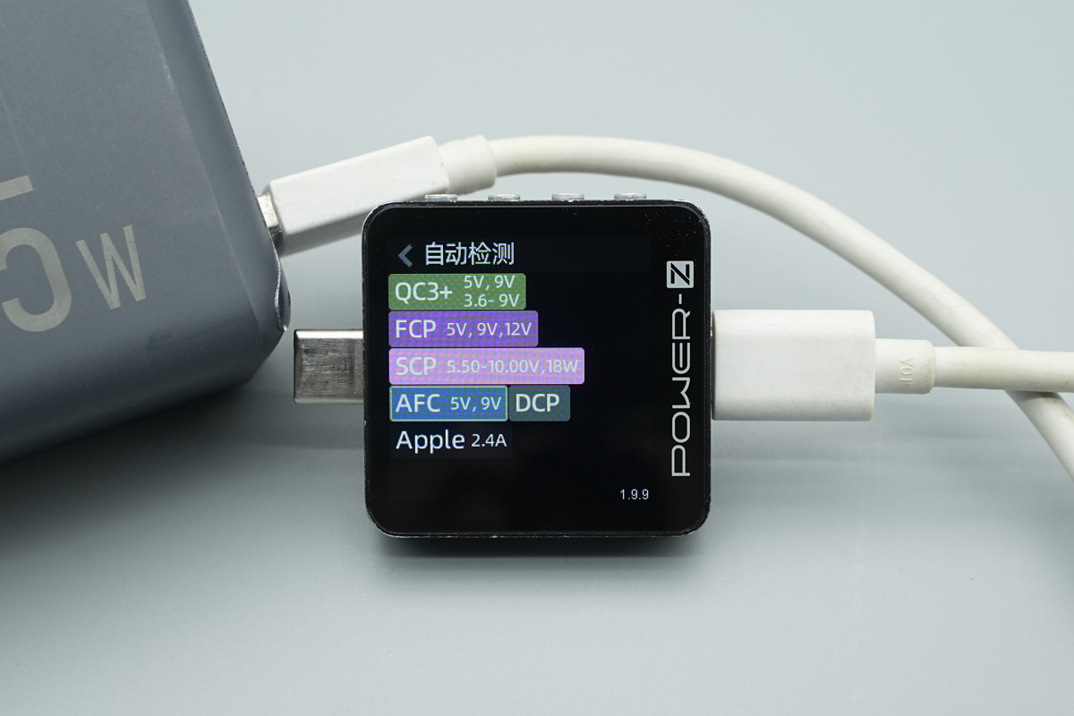
ChargerLAB POWER-Z KM003C shows that the USB-A port supports QC3+, FCP, SCP, AFC, Apple 2.4A and DCP.
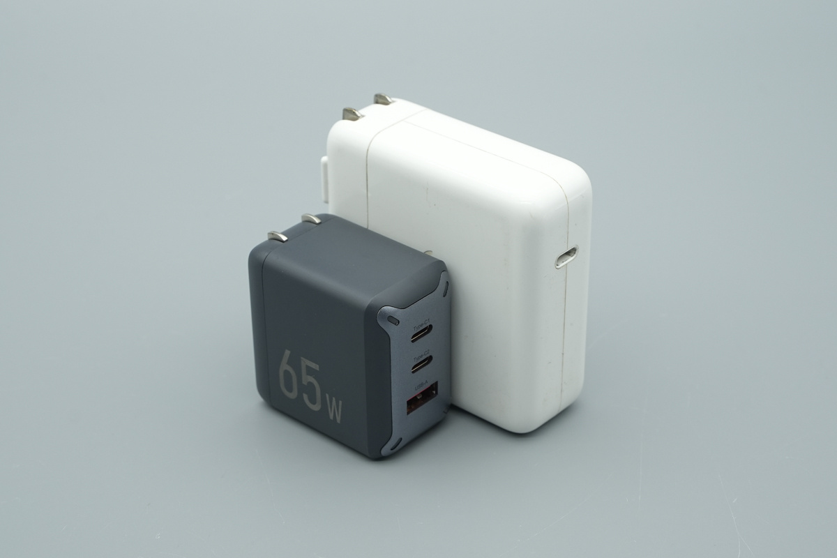
Put it with Apple’s 67W dynamic charger, it is remarkably smaller.
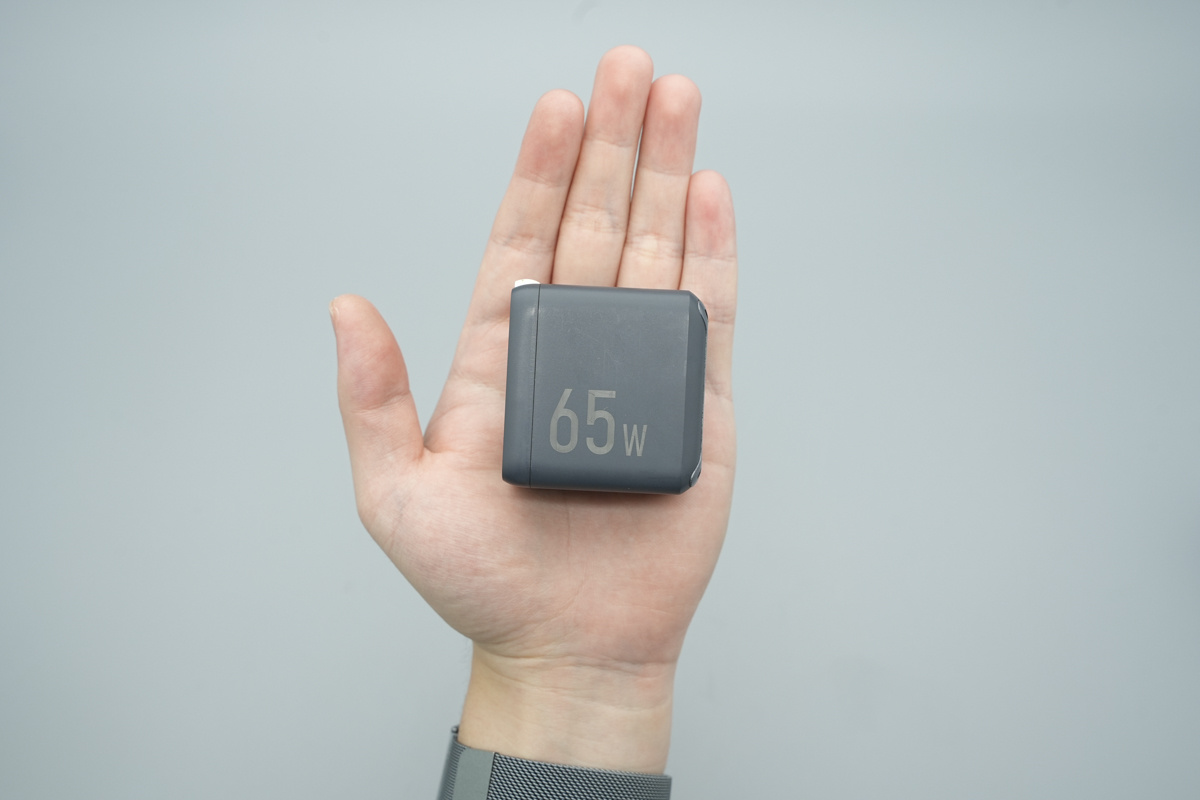
That's how big it is in the hand.
Now that we’ve wrapped up our quick look at the design and fast-charging compatibility, let's diving straight into the full internal teardown.
Teardown
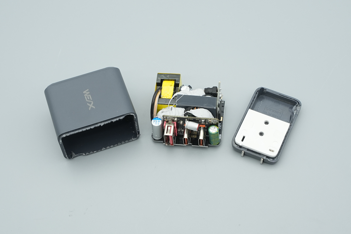
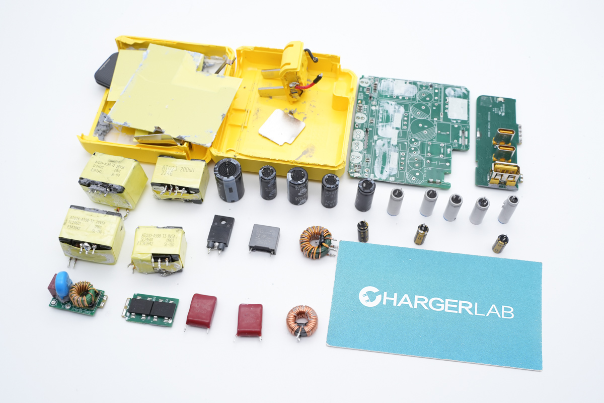
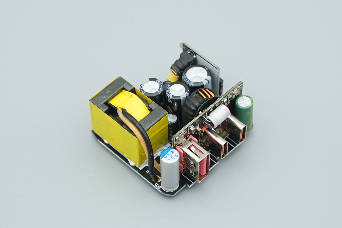
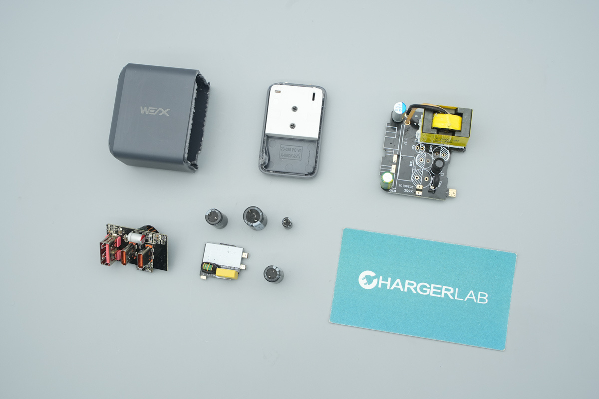
Moving to teardown, carefully pry open the housing to reveal the PCBA module inside.
The foldable pin module utilizes a plug-in connector interface to supply power to the PCBA.
On the PCBA front, wihte thermal potting compound is applied across the transformer and caps to anchor the components and optimize thermal management.
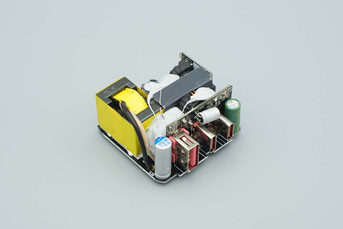
This is the side-profile view of the PCBA module.
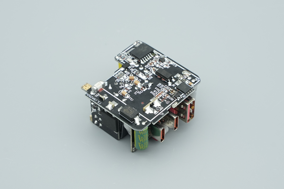
This is the rear view of the PCBA module, featuring key components including the primary master control chip, an optocoupler, synchronous rectifier controllers, and synchronous rectifier MOSFETs.
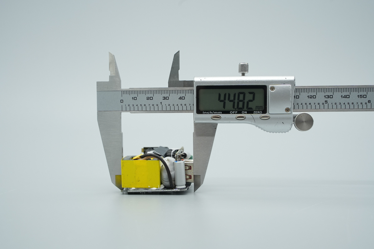
The length of PCBA is about 44.82mm (1.765 inches).
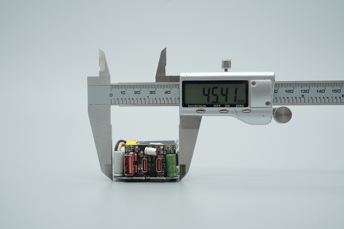
The width of PCBA is about 45.41mm (1.788 inches).
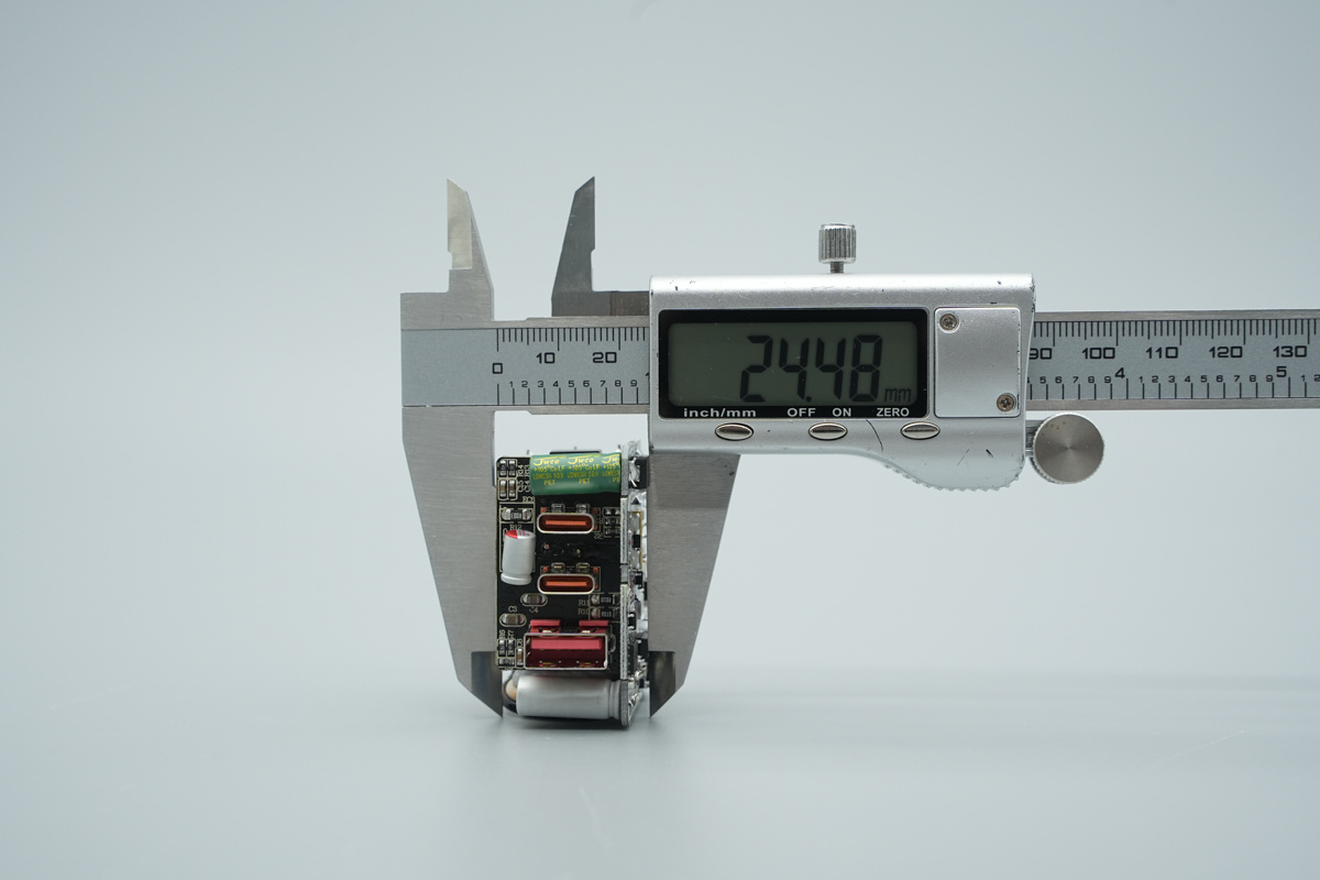
The thickness of PCBA is about 24.88mm (0.964 inches).
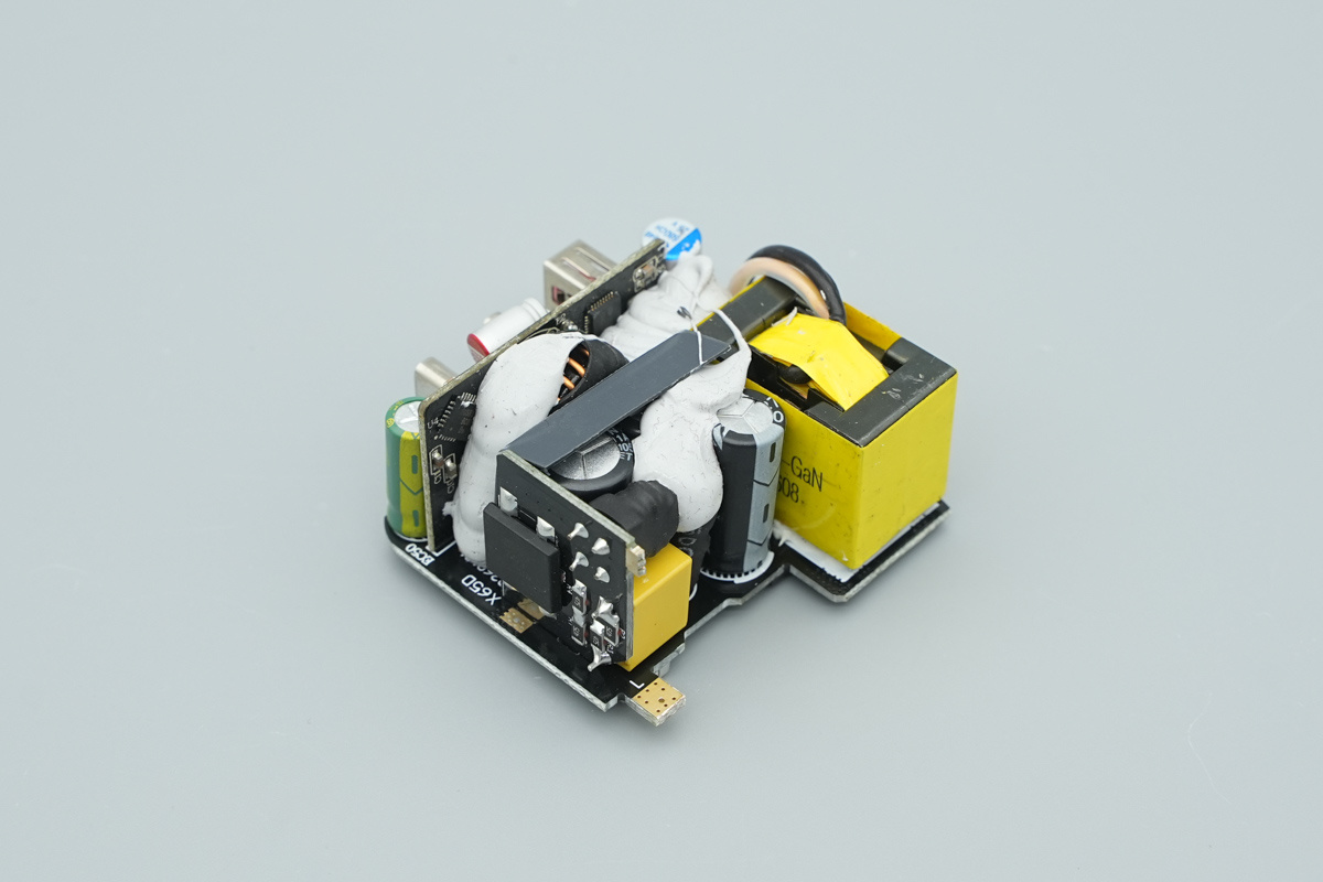
After removing the surface wihte thermal potting compound, the internal circuit architecture of the charger is clearly manifested.
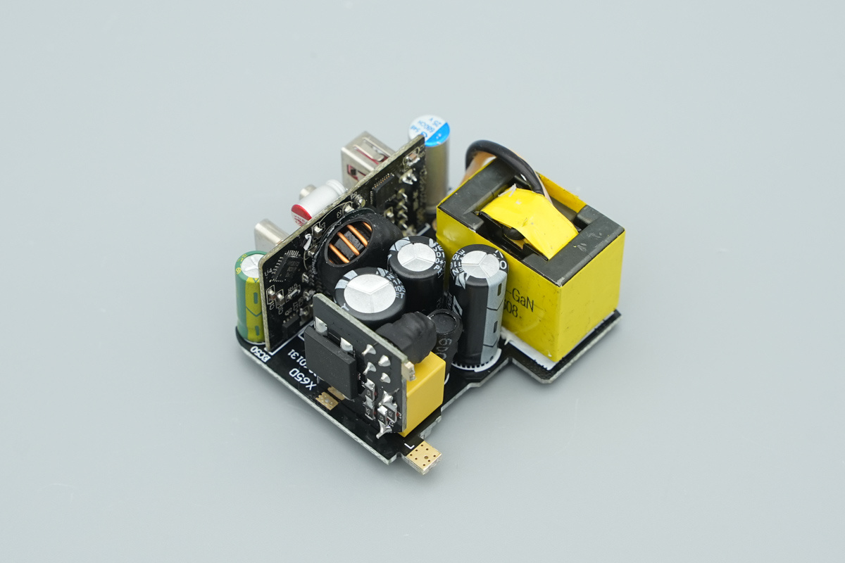
This reveals key electrical components, like input filtering elements, high-voltage filter caps, the main transformer, input end PCB and the output end step-down PCB.
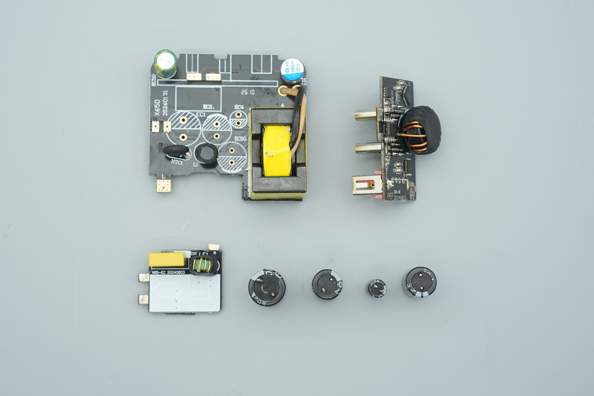
To get a clear look at the internal construction, we’ve disassembled the PCBA module, separating the input end PCB, output end PCB and caps.
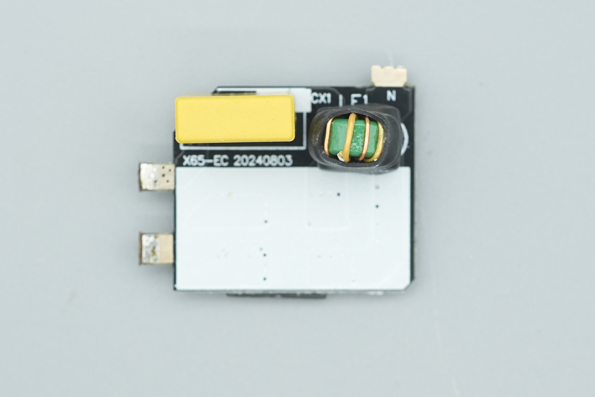
Front view of the input end PCB, it populated with a yellow X2 safety cap and a common-mode choke.
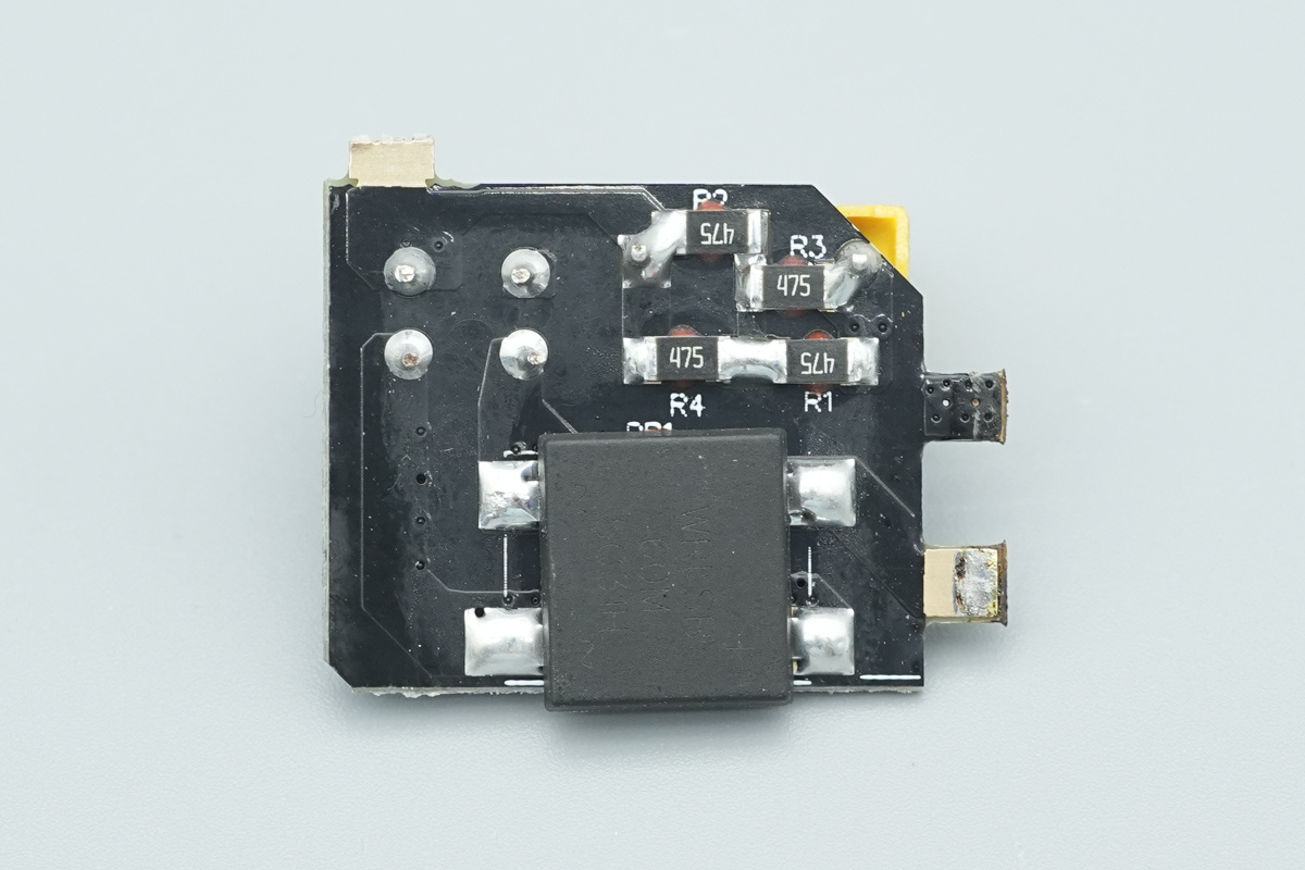
Rear view of the input end PCB, it features a rectifier bridge.
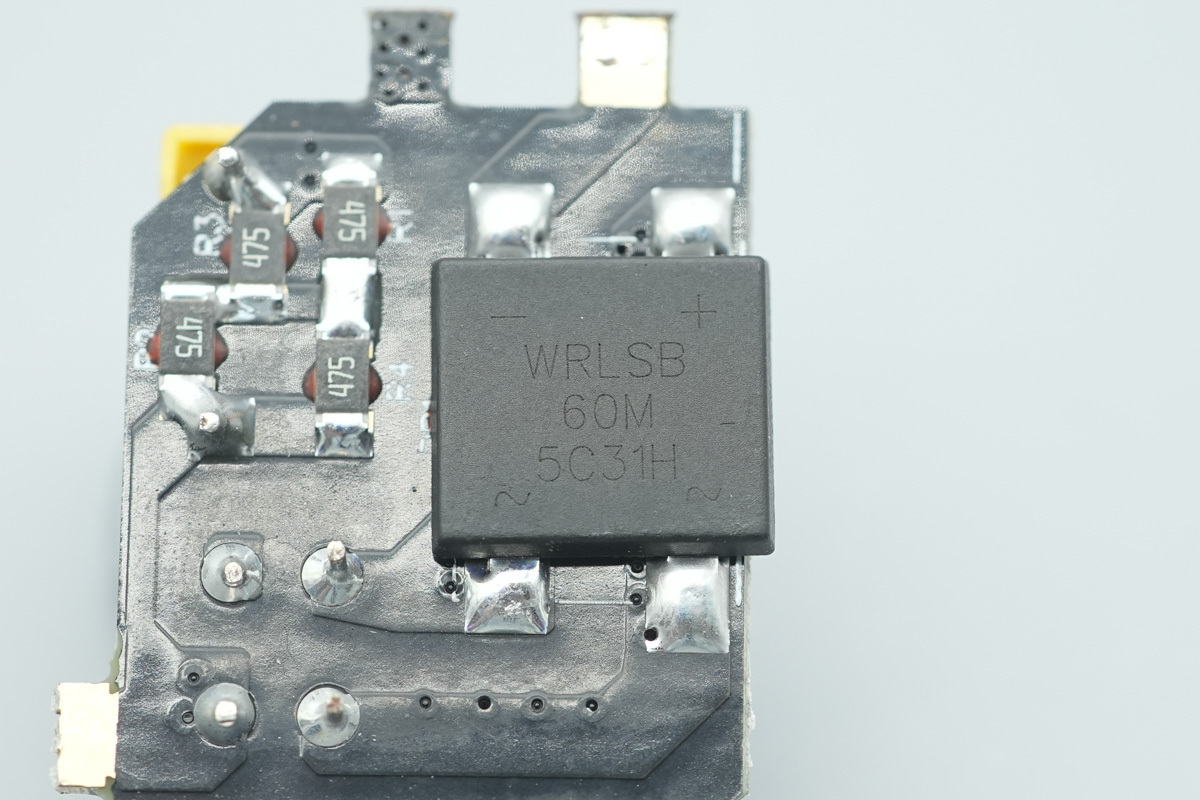
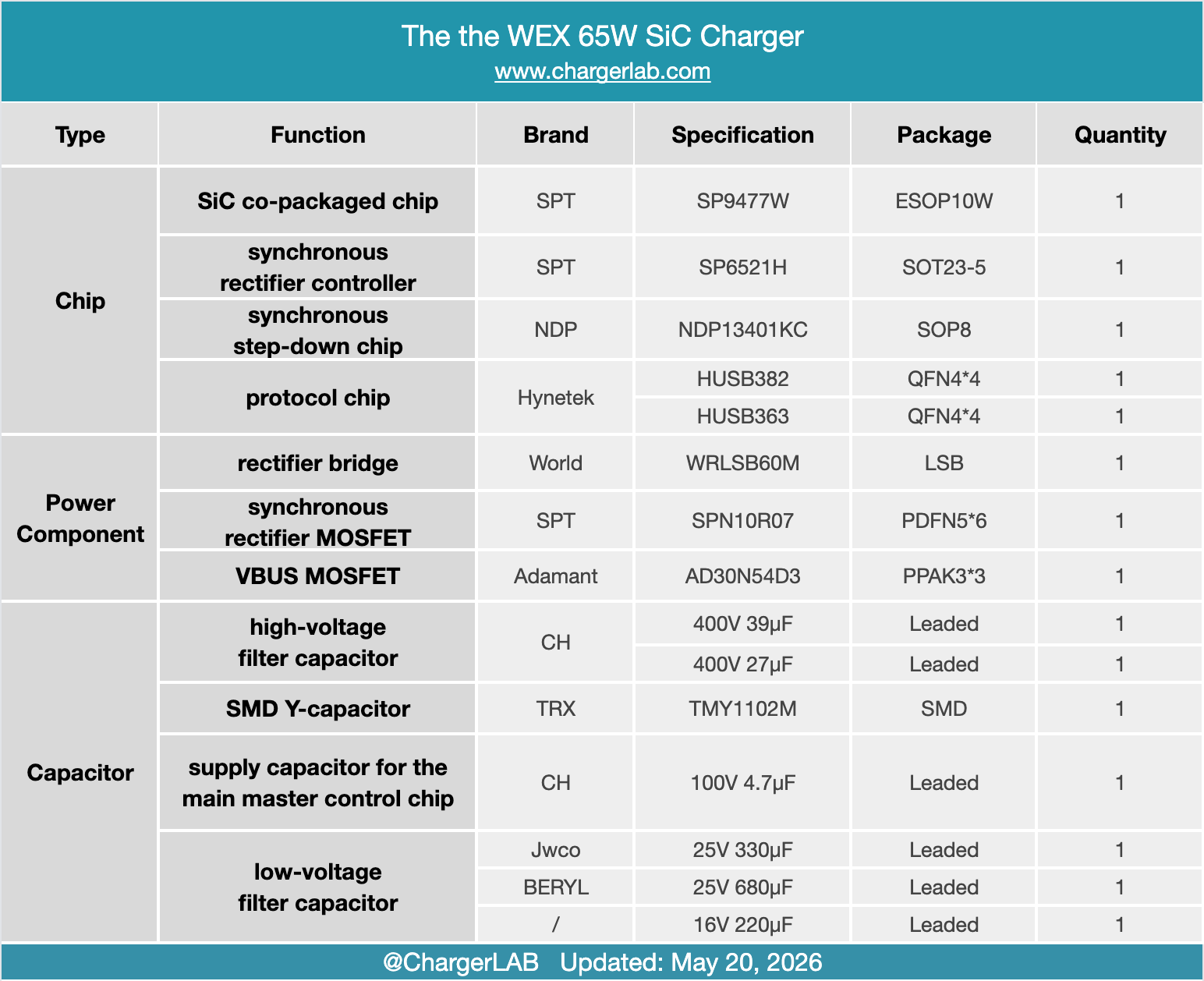
The rectifier bridge is from World, model WRLSB60M, 1000V and in an LSB package. This 'soft bridge' utilizes a soft recovery profile and smooth turn-off characteristics to minimize junction capacitance, effectively reducing harmonic oscillations and EMI noise.
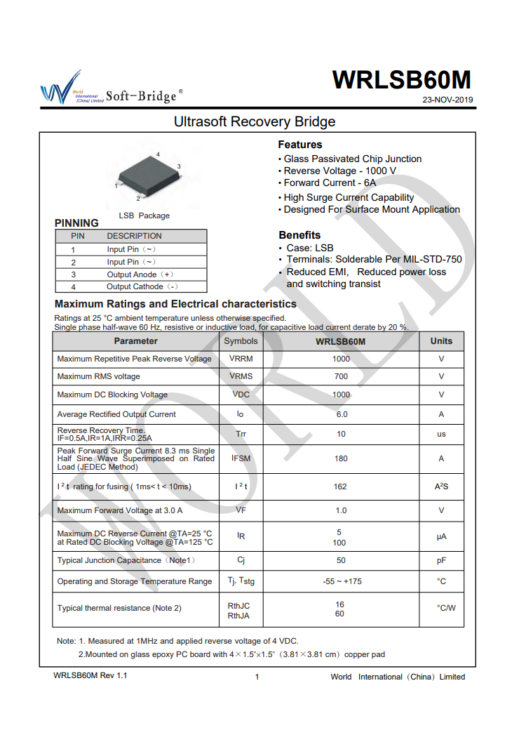
Here is the info about World WRLSB60Mr.
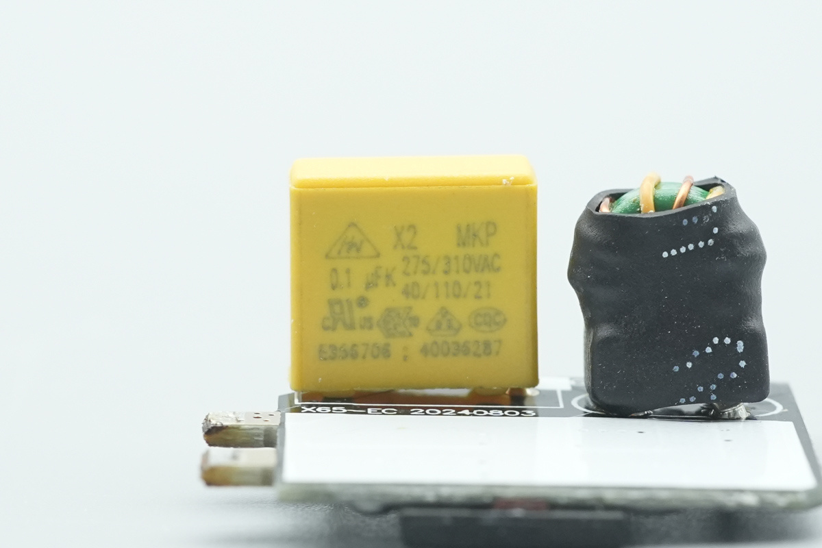
The X2 safety cap, 0.1μF.
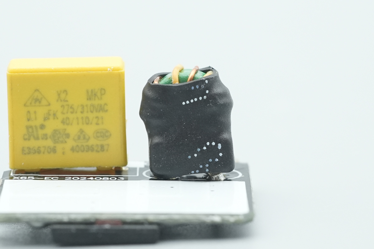
The common-mode choke is encapsulated in heat-shrink tubing for electrical insulation and is utilized to filter out EMI.
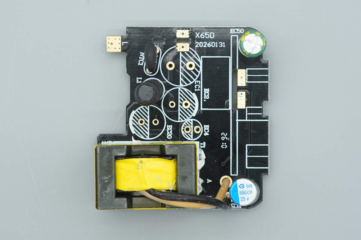
With the PCBs and select caps removed, the mainboard's core layout is revealed, featuring the transformer and two low-voltage output caps.
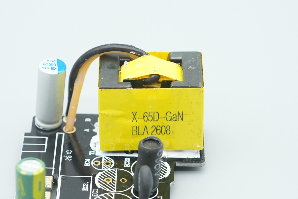
The high-frequency transformer, featuring yellow insulating tape, marked 'X-65D-GaN BLA 2608'.
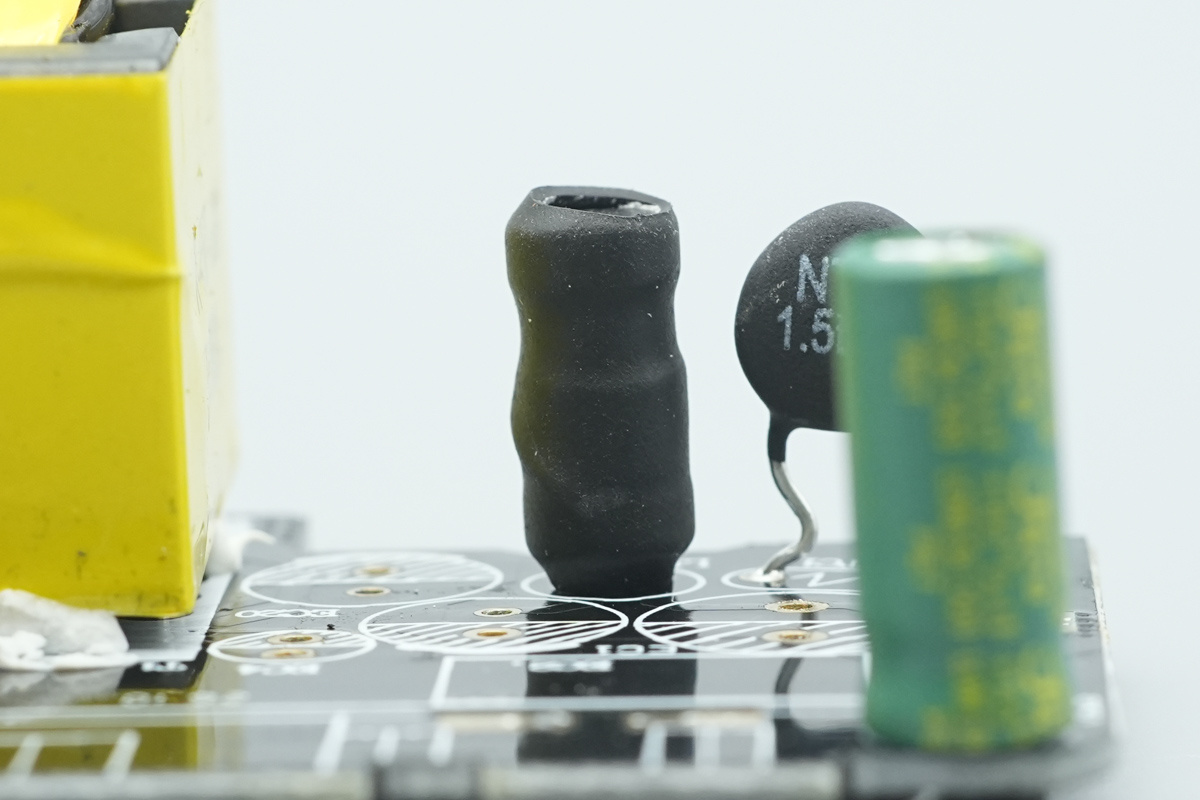
A I-shaped choke sits right next to the transformer.
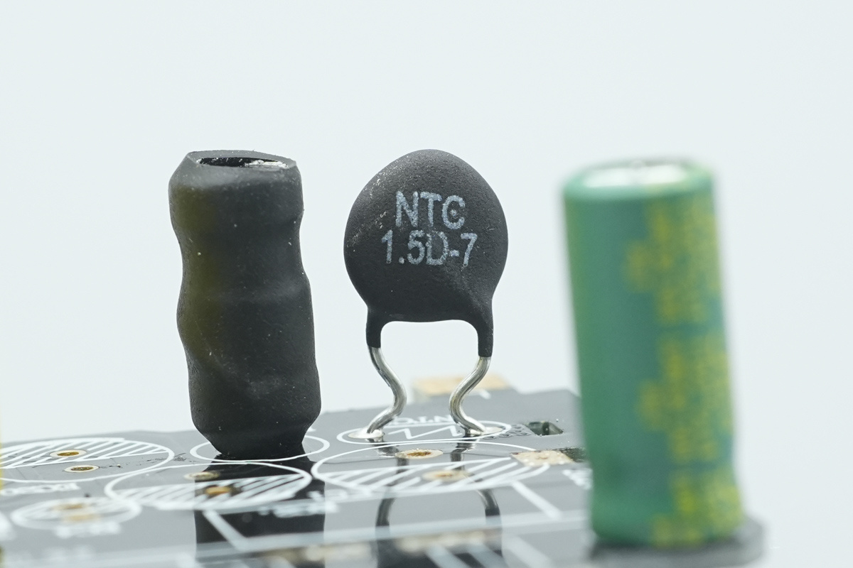
An NTC thermistor, marked 1.5D-7, is utilized to suppress inrush current during the charger's power-on sequence.
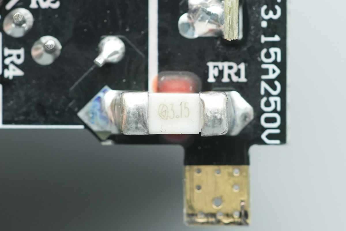
From rear side, it features a time-delay fuse at the input end, provided for OCP.
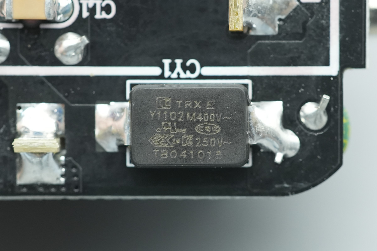
The SMD Y-cap is from TRX, model TMY1102M. Its small, lightweight design makes it an ideal component for maximizing space within the dense architecture of GaN fast chargers.
Here is the info about TRX SMD Y-cap.
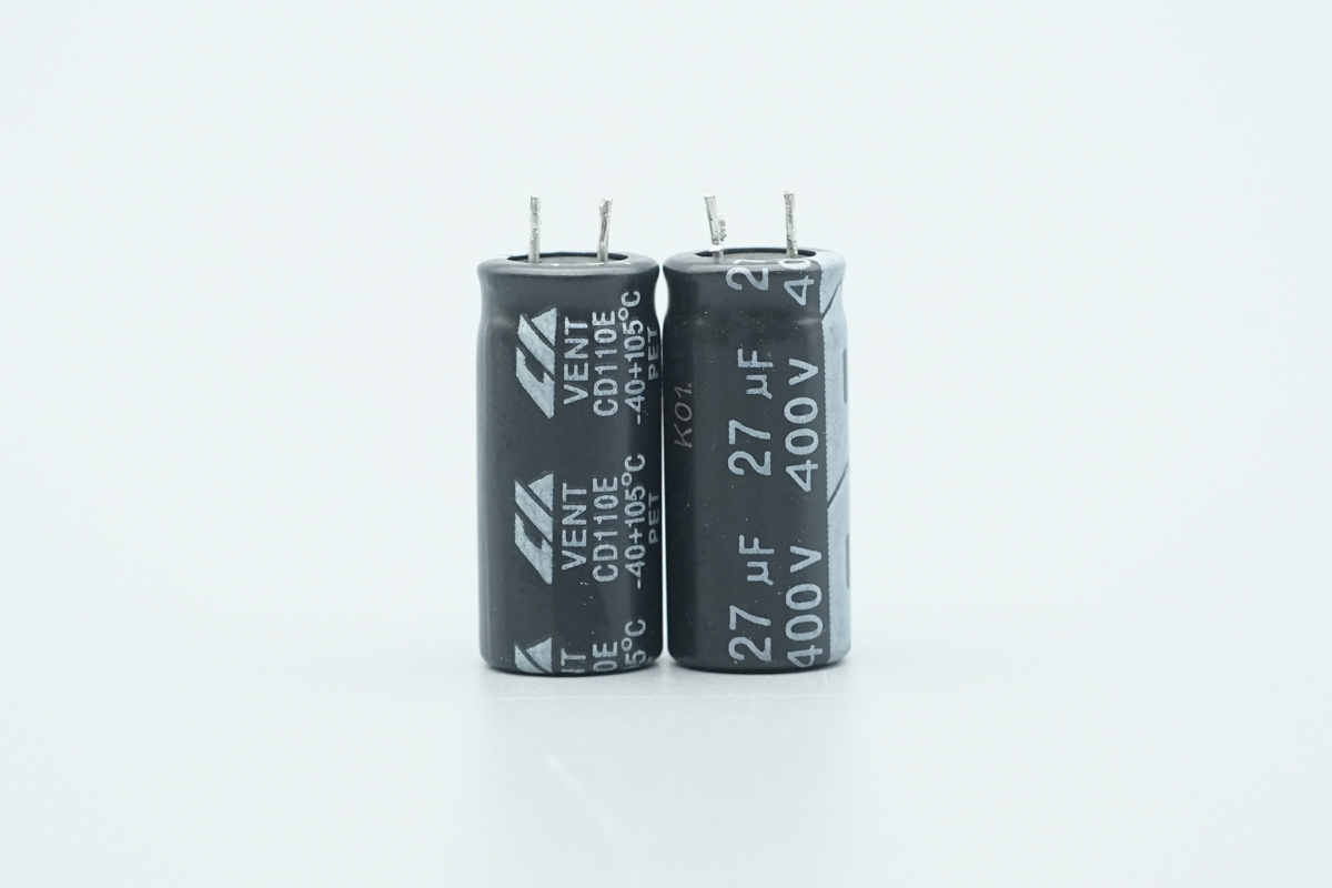
The input end utilizes two high-voltage filter caps from CH, 400V 39μF and 400V 27μF respectively .
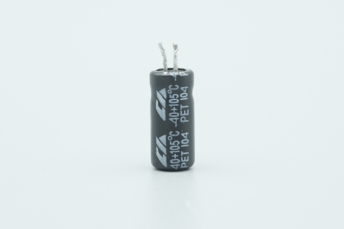
The supply cap for the main master control chip is from CH, 100V 4.7μF.
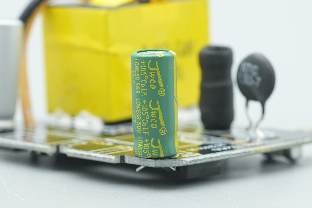
An additional aluminum electrolytic cap is from Jwco, 25V 330μF.
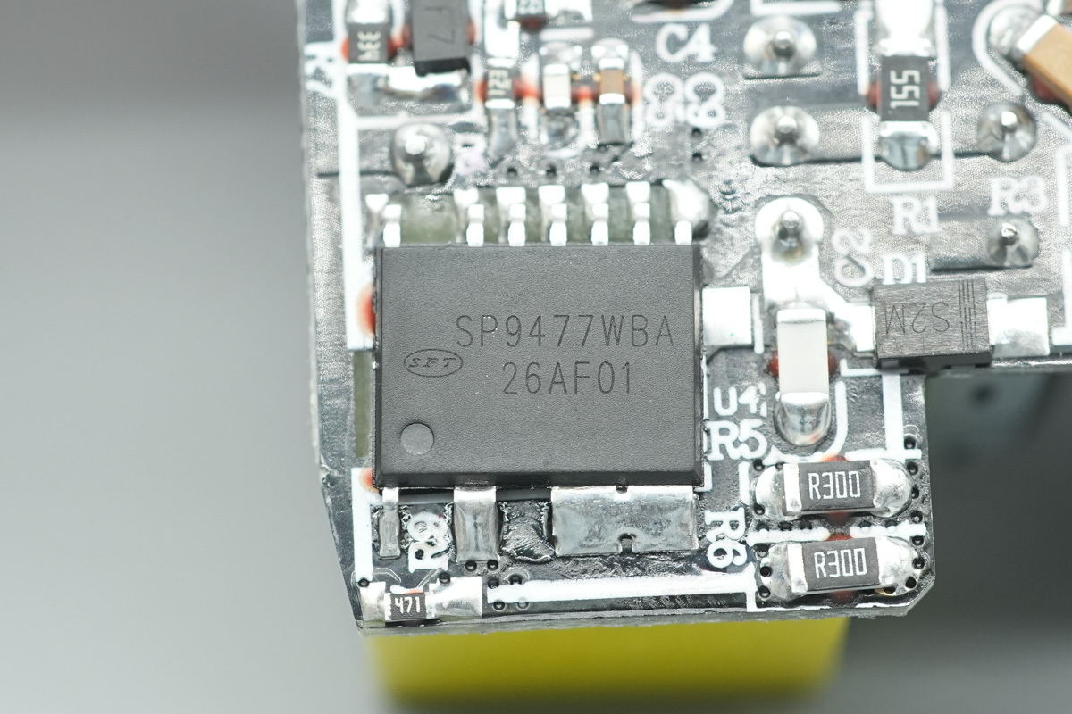
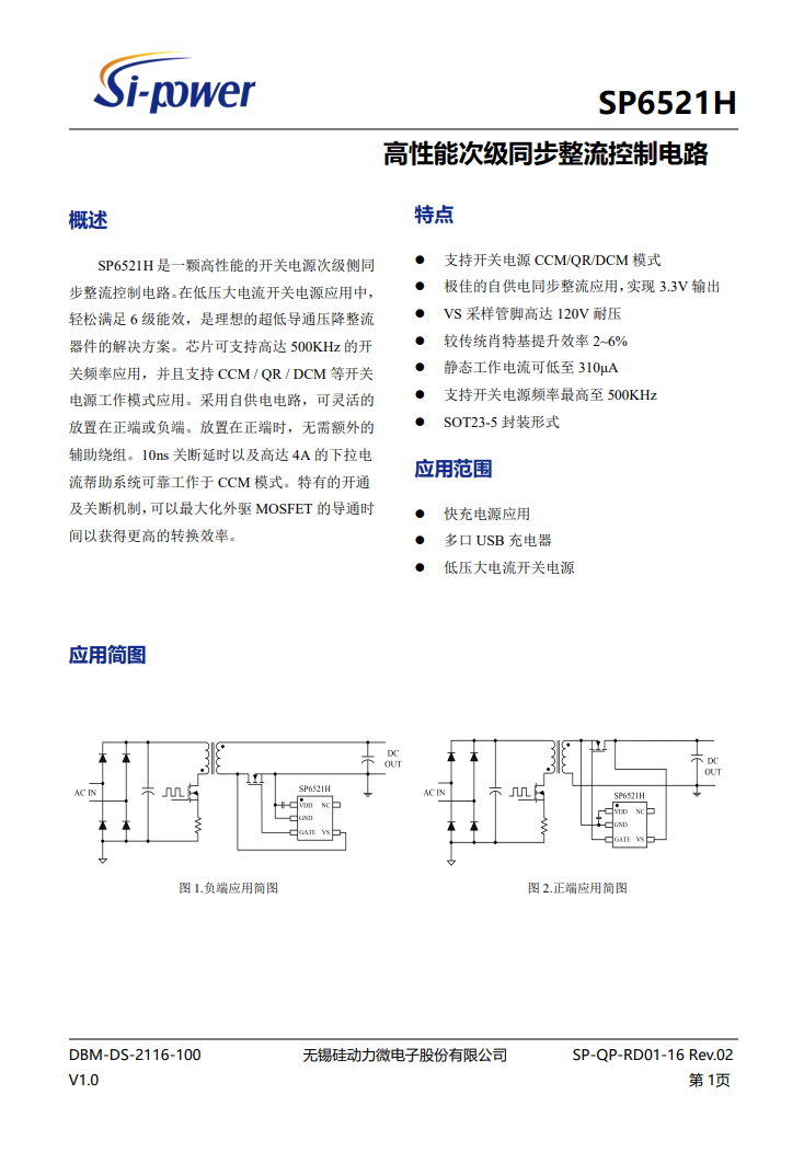
The SiC co-packaged chip is from SPT, model SP9477W, located on the rear of the mainboard,
It is specifically engineered for fast charging and adapter applications, integrating a 700V SiC power device and utilizing high-frequency QR technology to provide a high-performance solution for USB-PD and Type-C chargers.
The SP9477W simplifies design by integrating a 700V SiC power device. Its QR technology ensures silent operation, while intelligent switching to frequency-foldback and Burst modes boosts efficiency during light loads.
From input under/over-voltage protection to primary current limiting and thermal safety, the SP9477W offers all-around reliability. It also features dynamic drive adjustment to protect secondary rectifiers.
With integrated frequency jittering to tackle EMI and an ESOP10W heat-enhanced package, it is engineered for high performance and cooler operation.
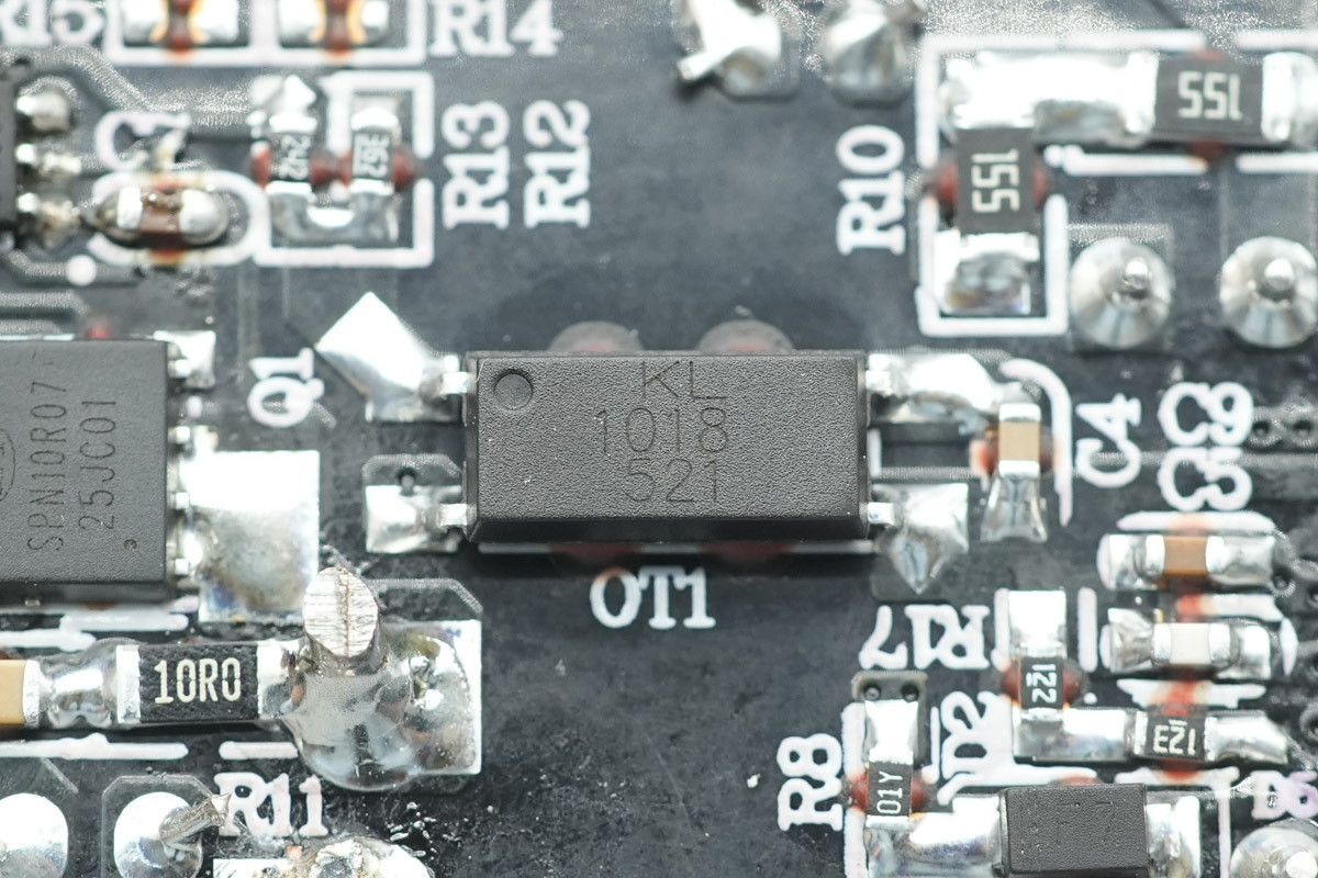
The optocoupler bridging the primary and secondary sides is from Kinglight, model KL1018.
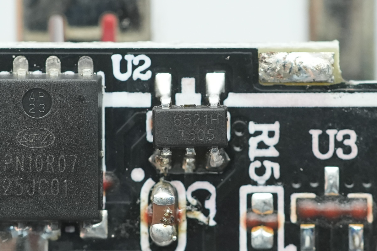
The synchronous rectifier controller is from SPT, model SP6521H, housed in an SOT23-5 package. Designed for high-current, low-voltage power conversion, it is a dedicated secondary-side synchronous rectifier controller to maximize efficiency.
With support for 500kHz switching and adaptive CCM/QR/DCM operation, it optimizes power conversion. Its smart self-supply design helps boost efficiency by 2–6% versus Schottky alternatives, keeping the design well within the requirements of Level VI efficiency.
It features an ultra-fast turn-off delay of 10ns and a robust 4A pull-down current, ensuring reliable performance in CCM operation. With a low quiescent current of 310μA, it is optimized for low-voltage, high-current applications, including fast-charging adapters and multi-port USB chargers.
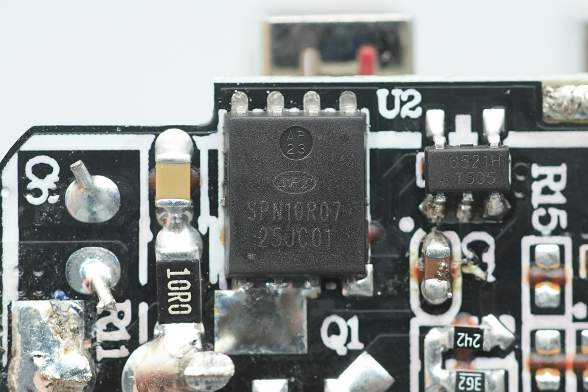
The synchronous rectifier MOSFET is from SPT, model SPN10R07, NMOS 100V and 7mΩ, in a PDFN5x6 package.
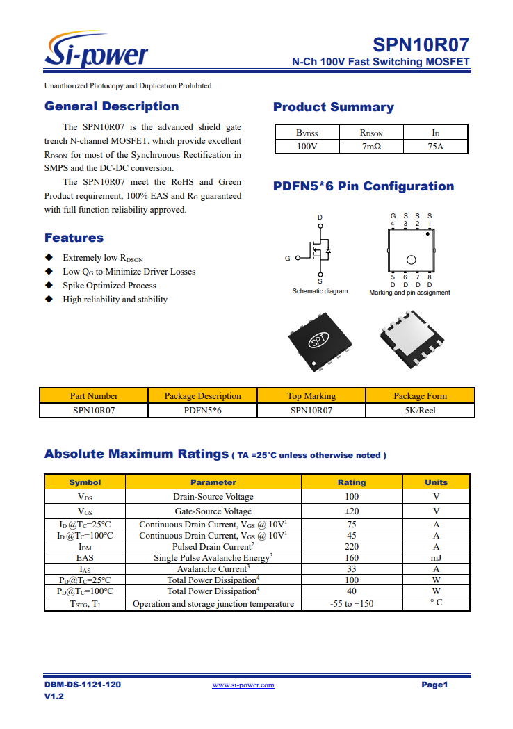
Here is the info about SPT SPN10R07.
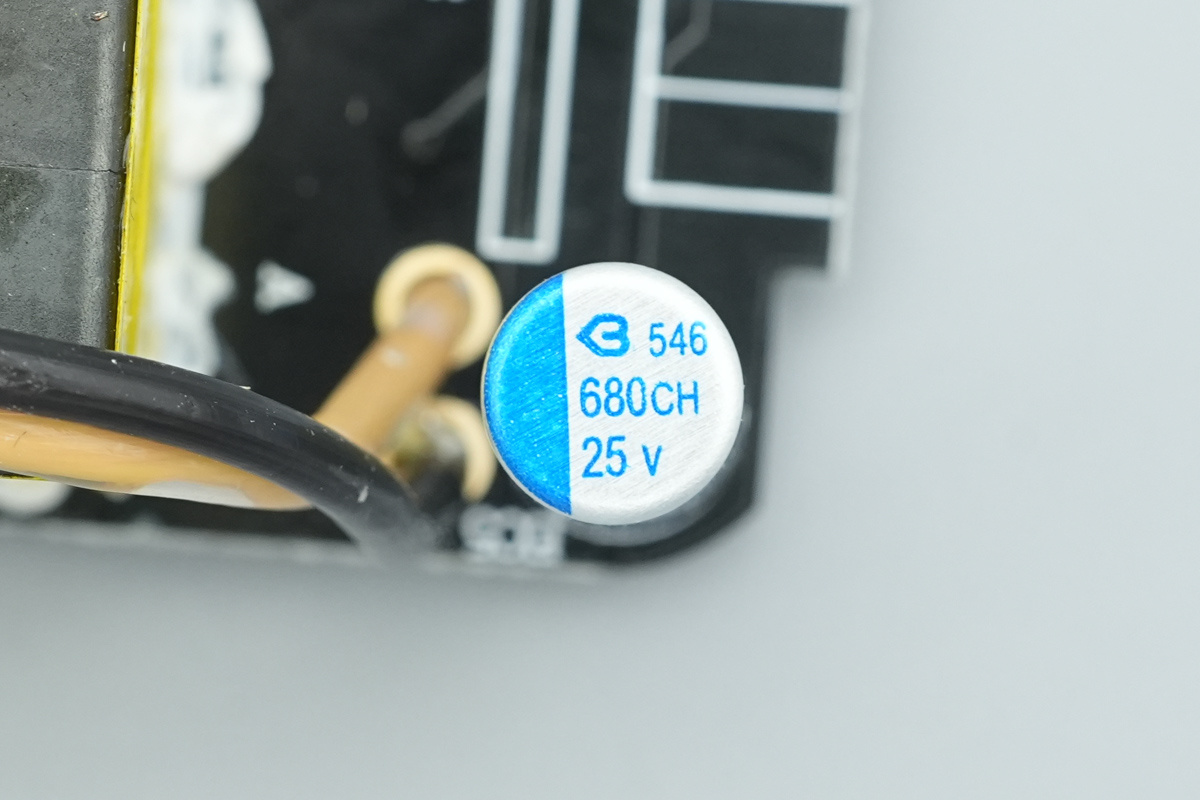
A blue solid filter cap is from BERYL , 25V 680μF.
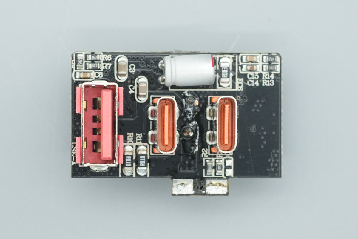
The output end step-down PCB features two USB-C ports and one USB-A port on its top side, accompanied by a solid filter cap.
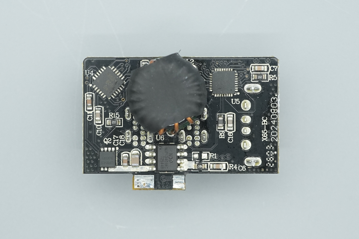
The rear of the output end PCB houses the protocol chip alongside a magnetic-core step-down choke, wrapped in heat-shrink tubing, for multi-port secondary voltage regulation.
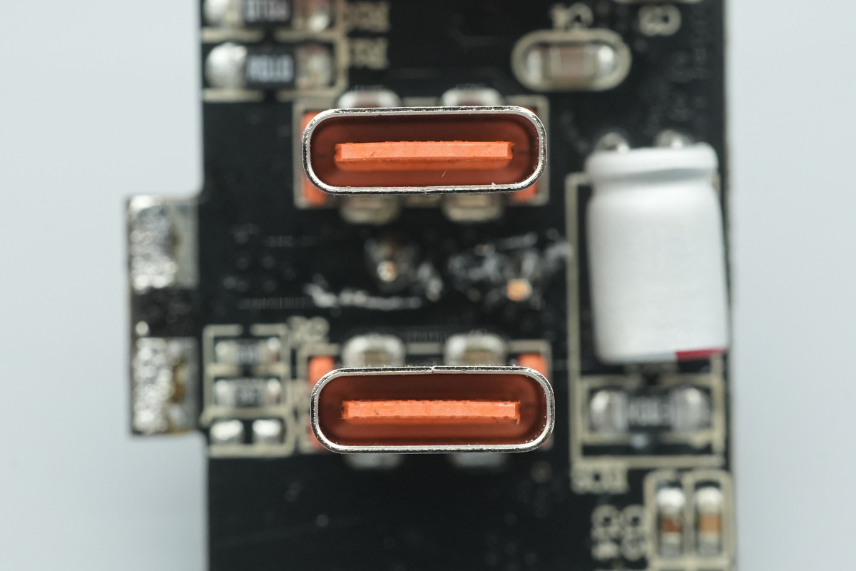
These are two USB-C ports, both featuring the orange plastic sheets within the internal architecture.
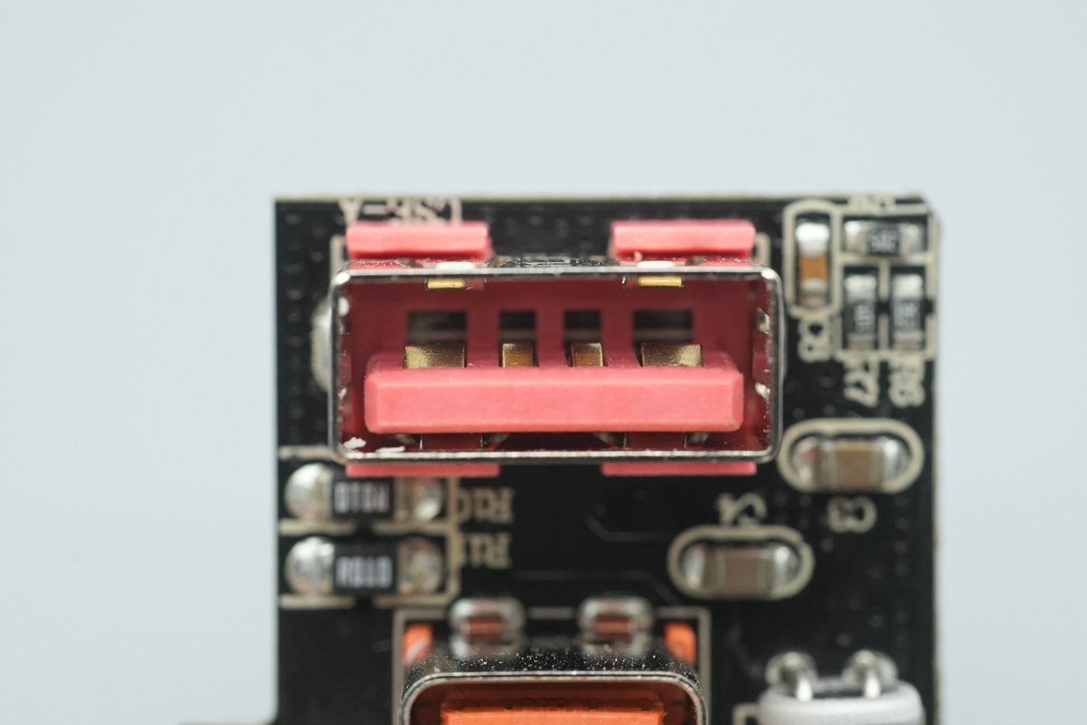
The USB-A receptacle features reinforced, widened power pins to ensure minimal contact resistance and facilitate high-current delivery for fast charging.
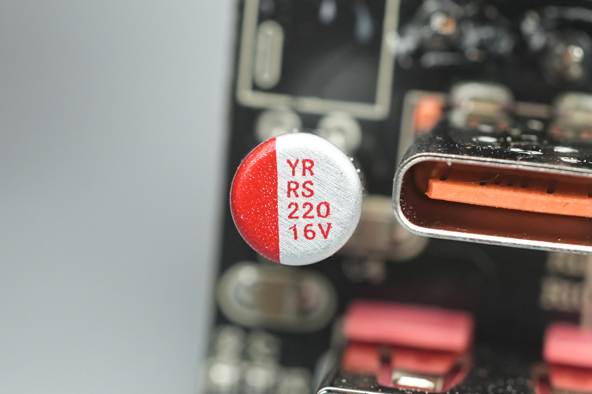
This is a solid filter cap on the output end, 16V 220μF.
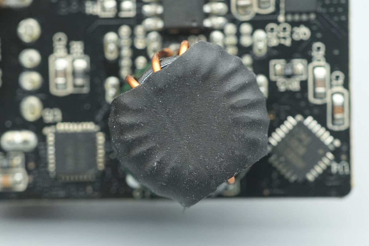
The step-down magnetic choke, with heat-shrink tubing for insulation and protection.
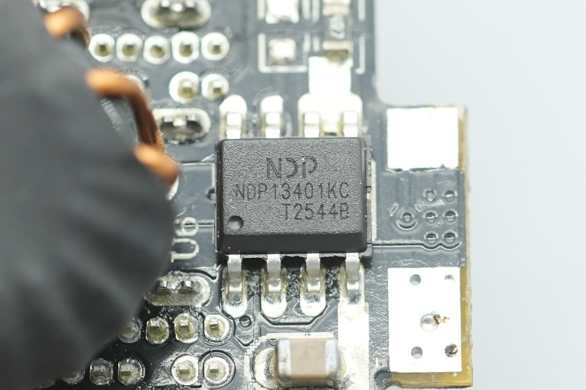
The synchronous step-down chip is from NDP, model NDP13401KC, featuring constant-frequency, average-current mode control. It is housed in an SOP8 package.
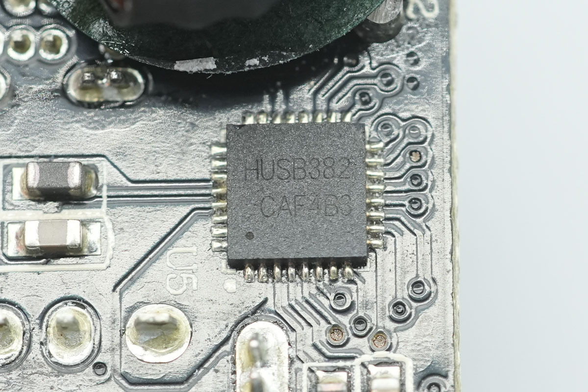
The protocol chip for USB-C2 and USB-A is from Hynetek, model HUSB382. This high-performance, highly integrated chip features built-in VBUS MOSFETs, which simplifies the peripheral circuit design by eliminating the need for external power path management.
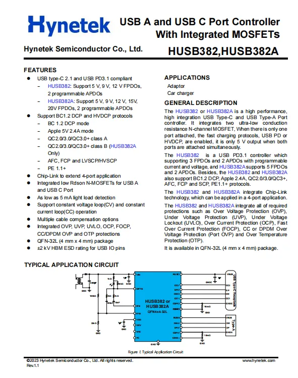
The HUSB382 integrates a comprehensive protection suite, including OVP, UVP, UVLO, OCP, FOCP, CC/DPDM pin OVP and TSD. Housed in a QFN4x4-32L package, it is specifically optimized for compact multi-port fast chargers and automotive charging applications.
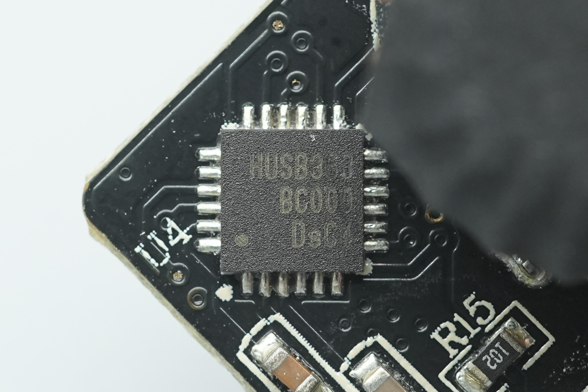
The protocol chip for the USB-C1 port is from Hynetek, model HUSB363. It supports multiple programmable PDOs, allowing for dynamic voltage and current configuration to meet diverse application requirements, including full support for PPS PDOs
All PDOs are fully compliant with the USB PD 3.2 spec. Furthermore, it integrates DPDM charging protocols, allowing the D+ and D- pins to be configured for support of QC2.0, QC3.0, AFC, FCP, and Divider 3 modes, ensuring robust backward compatibility for legacy devices.
It features an integrated gate driver for secure VIN-to-VBUS power delivery, plus high-voltage tolerance across all critical signal pins (CC1/CC2/D+/D-), creating a multi-layered shield that keeps connected devices protected against electrical surges.
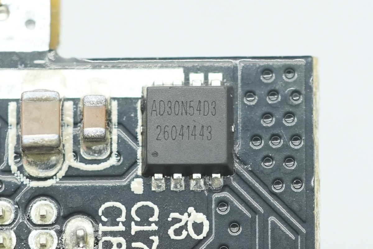
The VBUS MOSFET is from Adamant, model AD30N54D3, NMOS, 30V and 5.7mΩ, housed in a PPAK3x3 package.
Well, those are all components of the WEX 65W SiC Charger.
Summary of ChargerLAB
Minimalist and professional, the WEX 65W SiC charger comes in sophisticated black and gray finishes. With its space-saving foldable plug and a remarkably compact form factor, it is a travel-ready solution that doesn't compromise on power.
The device features a versatile two USB-C and one USB-A interface configuration, ensuring comprehensive compatibility with major fast-charging standards including PD, PPS, QC, and SCP. The USB-C1 port is capable of a Max output power of 65W, providing robust support for ultrabooks and a wide array of mobile electronics.
Teardown analysis reveals a multi-PCB stacking architecture. The primary side integrates the SPT SP9477W SiC co-packaged chip, while the secondary side adopts a high-efficiency solution from SPT, featuring the SP6521H synchronous rectifier controller paired with the SPN10R07 MOSFET.
The input end utilizes a WRLSB60M soft rectifier bridge from Wald and SMD Y-caps from TRX, optimizing PCB space efficiency. The secondary step-down and protocol control stage is powered by NDP's NDP13401KC, coupled with two protocol chips from Hynetek for independent multi-port management. High- and low-voltage filtering caps are from CH, Jwco, and BERYL, ensuring reliable ripple suppression and stable DC output.
In conclusion, this 65W SiC charger strikes an ideal balance between performance, reliability, and portability. It is an exemplary multi-port power solution for users demanding both high-efficiency charging and everyday convenience.
Related Articles:
1. Teardown of Xiaomi 33W USB-A Charger (MDY-16-EF)
2. V.2.0.1 | The New Software Version of ChargerLAB POWER-Z KM003C
3. Review of TALIX Zeta 240W PD3.2 Charger