Introduction
Today, we disassemble a Torras charger. The charger is equipped with a USB-C port and a retractable cable, both of which support a maximum output of 67W. It also supports a 45W+20W power distribution scheme, which is sufficient to meet the fast-charging requirements of laptops, tablets, and smartphones. Next, we will take a closer look at the design of this product.
Product Appearance
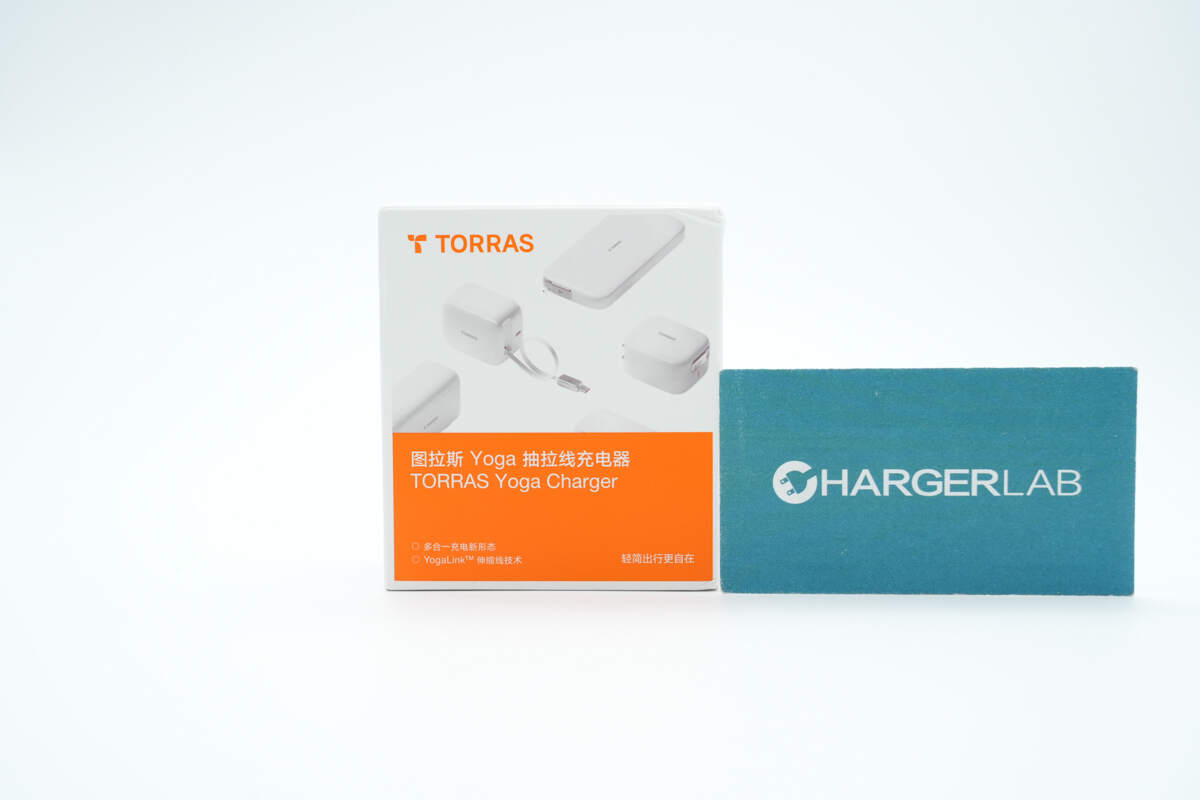
The front of the packaging box is printed with the TORRAS logo, the product's appearance, the product name, and key selling points.
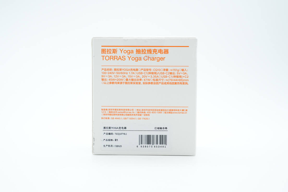
The back of the packaging box is printed with product specifications and other related information.

The package contains the charger and a user manual.
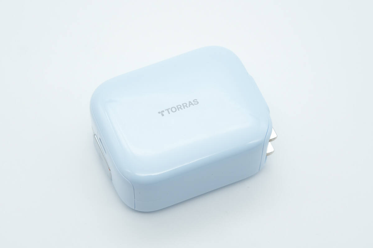
The housing is blue with a glossy surface and smoothly rounded edges.
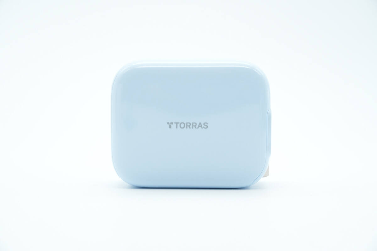
The TORRAS logo is printed at the center of both the front and back sides.
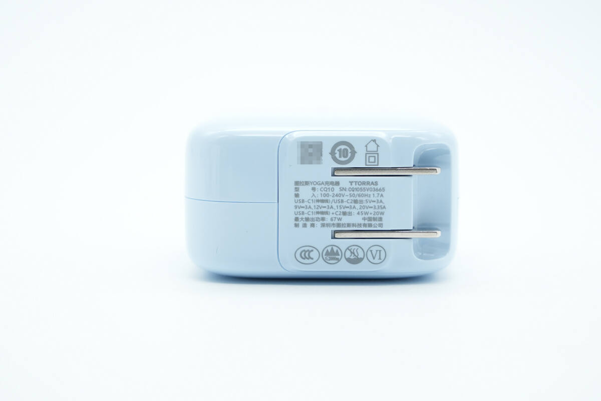
The input-side housing is printed with specification parameters.
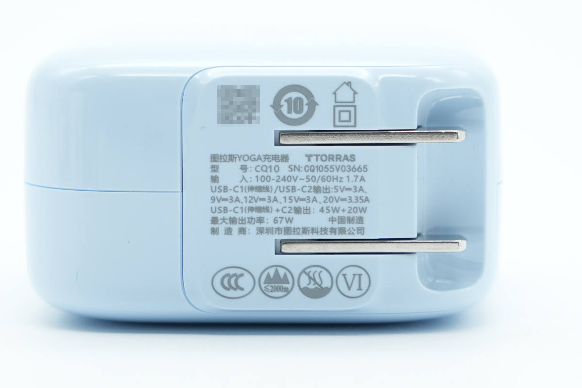
Model: CQ10
Input: 100-240V~50/60Hz 1.7A
USB-C1 cable/C2: 5V3A, 9V3A, 12V3A, 15V3A, 20V3.35A
USB-C1 cable+C2: 45W+20W
Maximum output power: 67W
The product has passed CCC certification and Level VI energy efficiency certification.
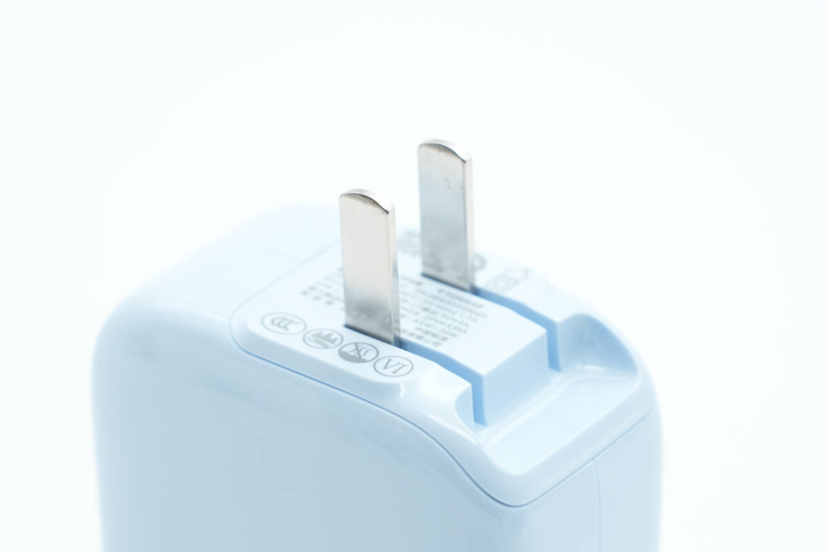
It is equipped with foldable prongs.
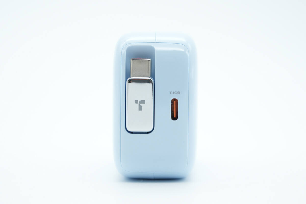
The other end is equipped with a USB-C port and a retractable cable.
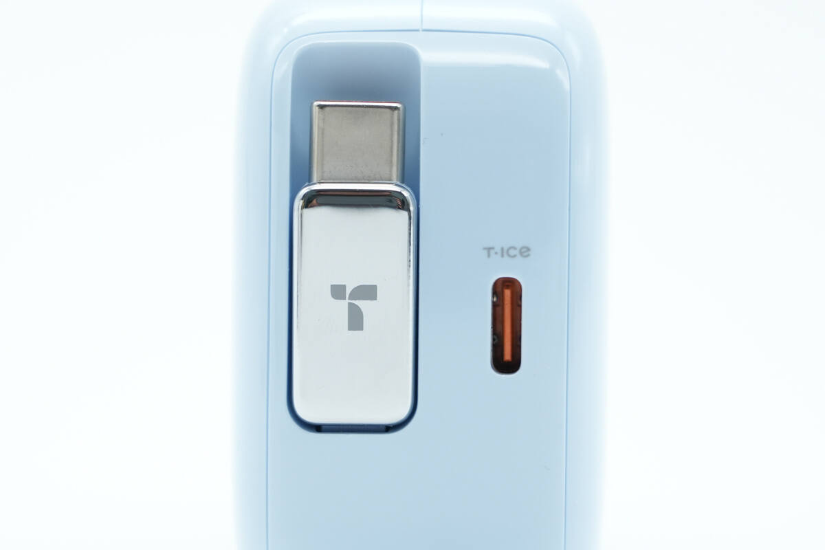
The retractable cable connector features a metal housing with a bright silver finish. A storage slot allows the connector to be magnetically secured.
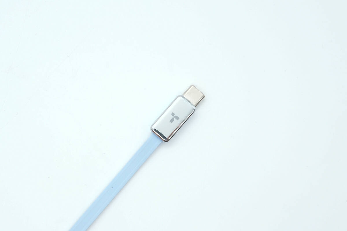
The cable features a flat design.
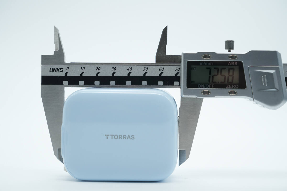
The length of the charger is about 72.58 mm (2.86 inches).
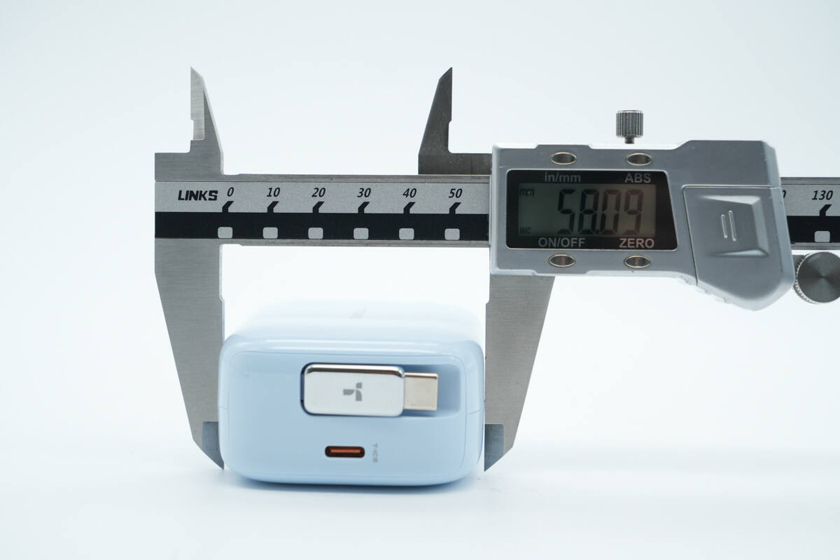
The width is about 58.09 mm (2.29 inches).
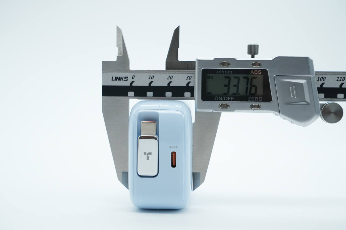
The thickness is about 33.76 mm (1.33 inches).
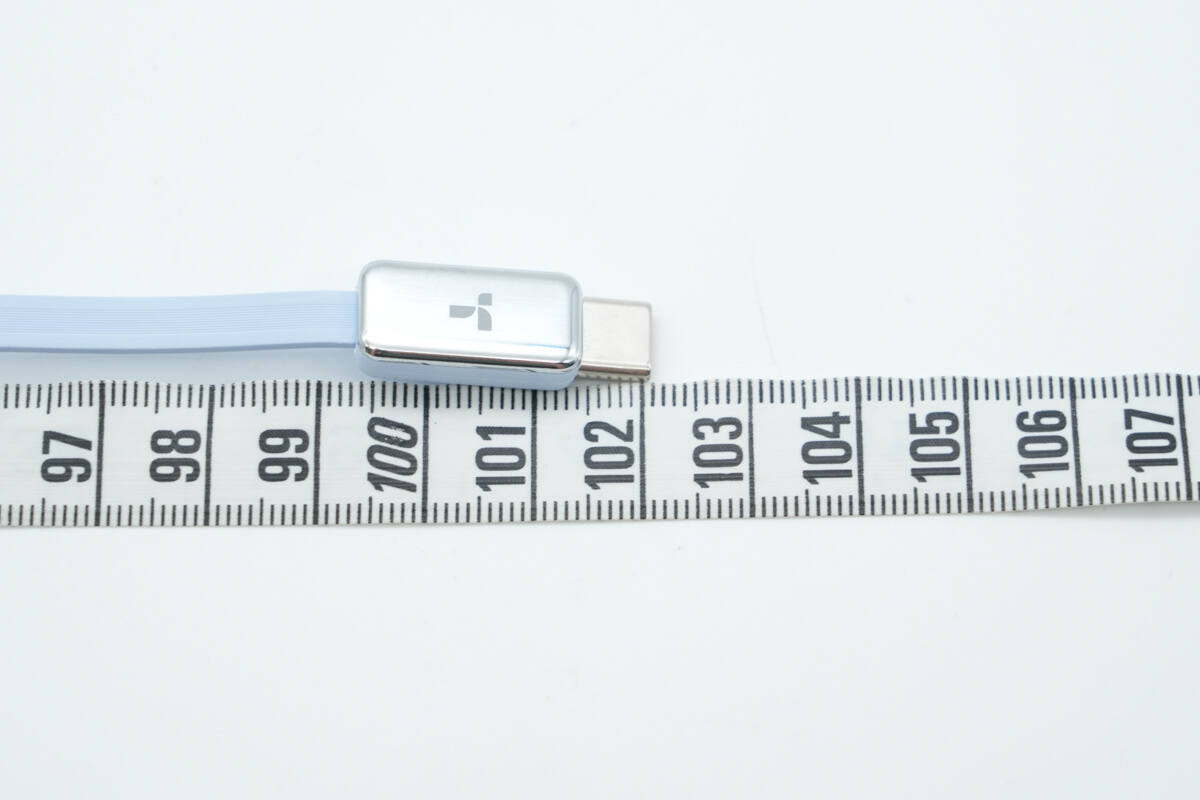
The length of the retractable cable is about 102 cm (40.16 inches).
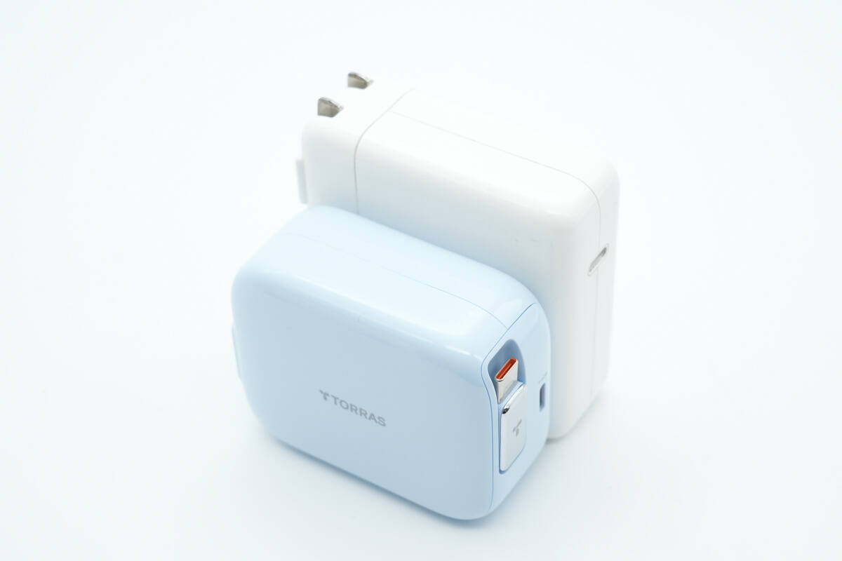
Compared with the Apple 67W charger, its size advantage is obvious.

That's how big it is on the hand.
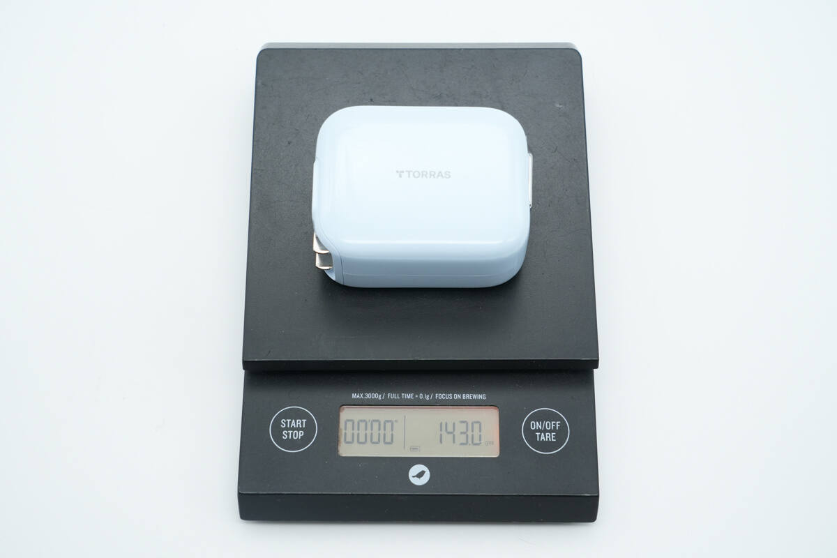
The weight is about 143 g (5.044 oz).
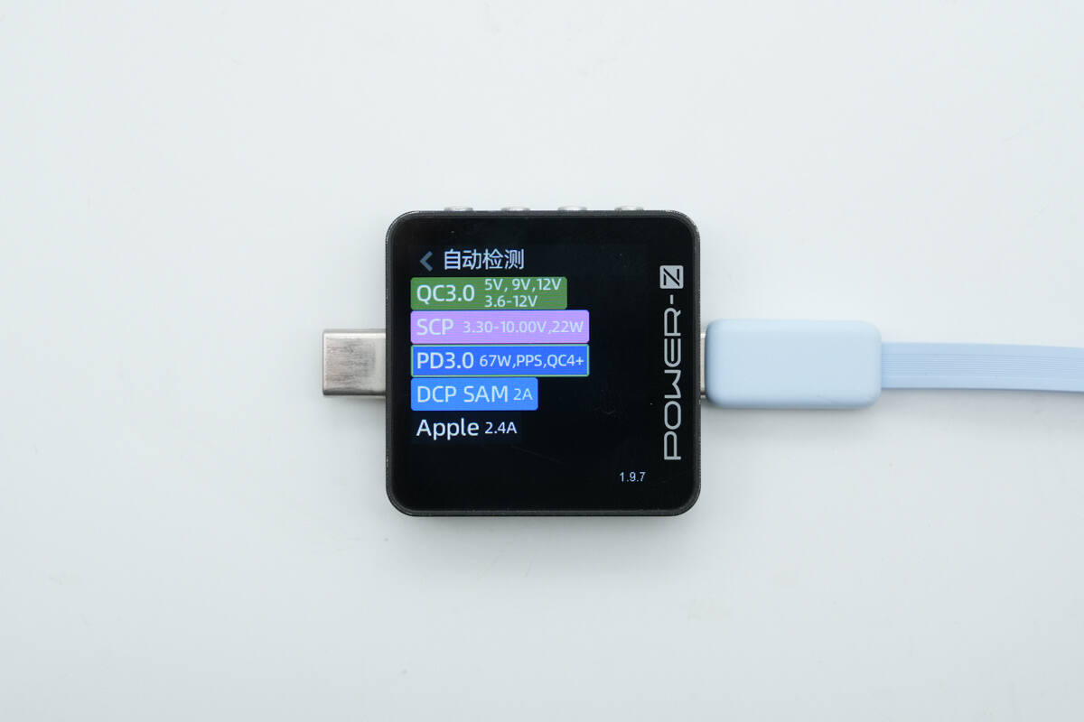
ChargerLAB POWER-Z KM003C shows that the retractable cable supports QC3.0/4+, SCP, PD3.0, PPS, DCP, SAM 2A, and Apple 2.4A charging protocols.
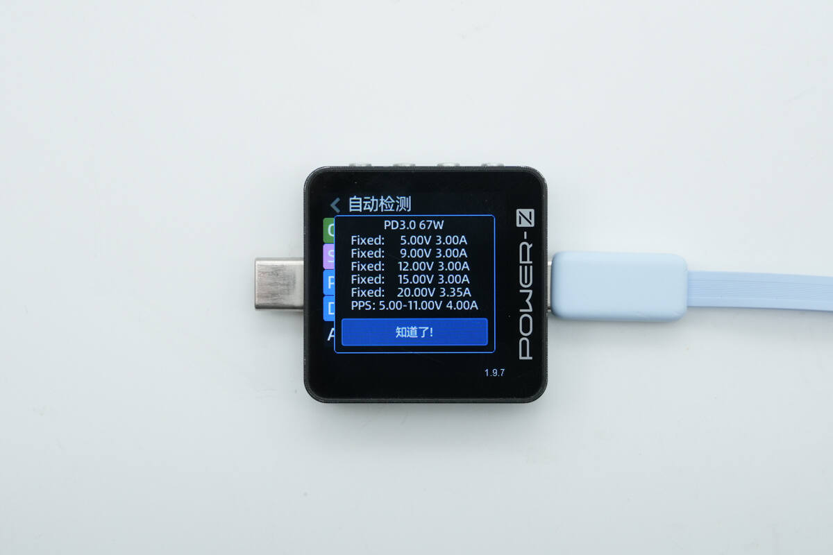
It has five fixed PDOs of 5V3A, 9V3A, 12V3A, 15V3A, and 20V3.35, as well as one set of PPS, which is 5-11V4A.
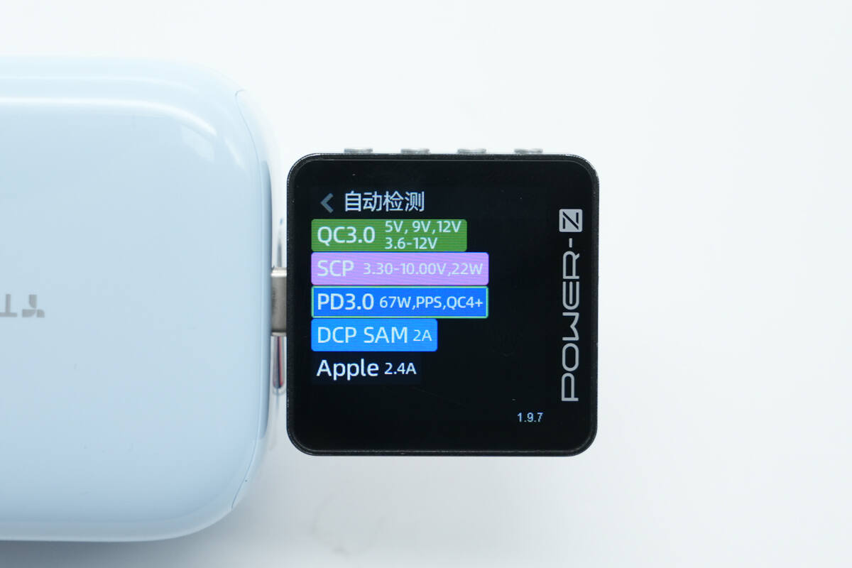
The USB-C port supports the same charging protocols as the retractable cable.
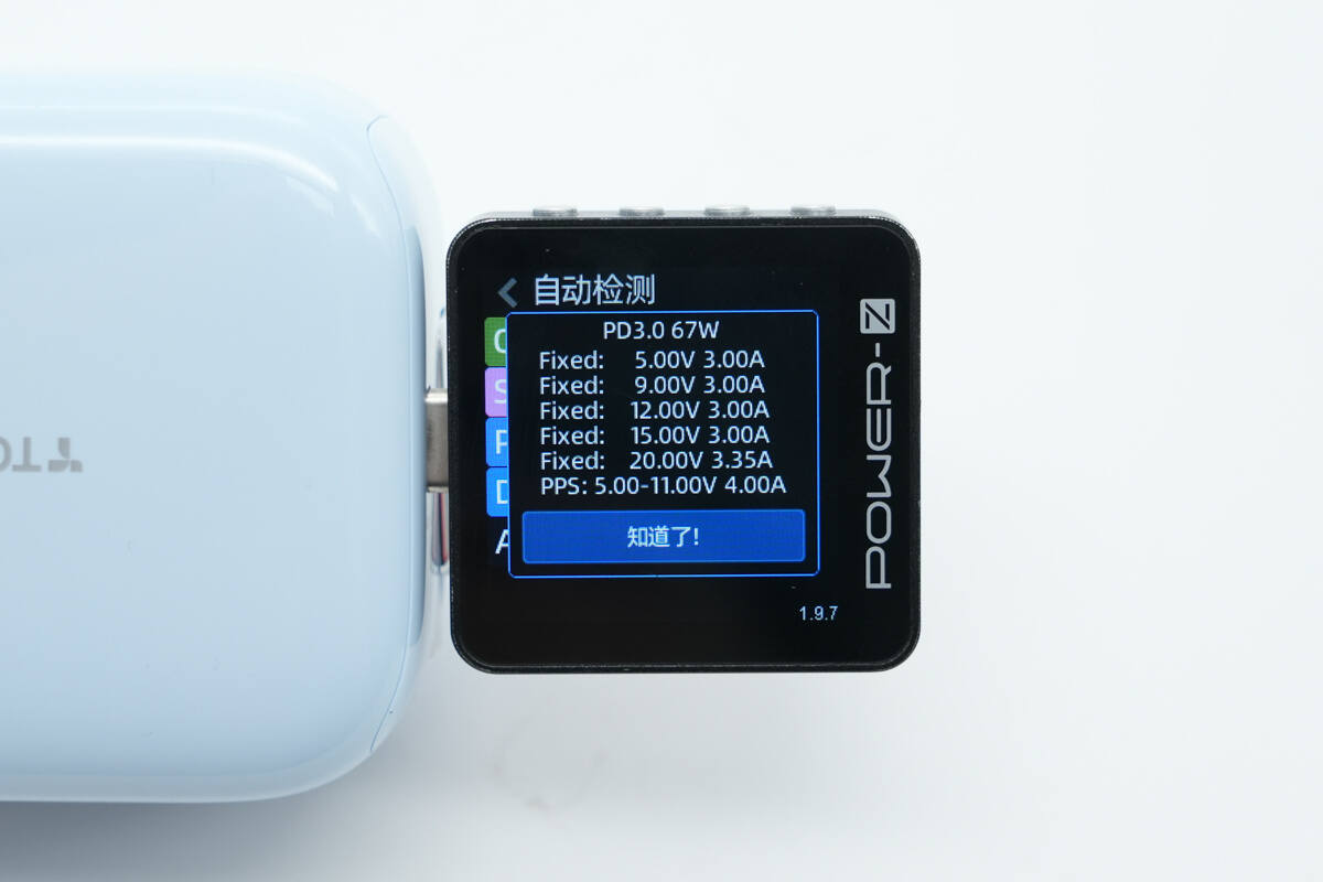
The PDO reports are identical as well.
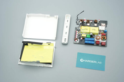
Teardown
Next, let's take it apart to see its internal components and structure.

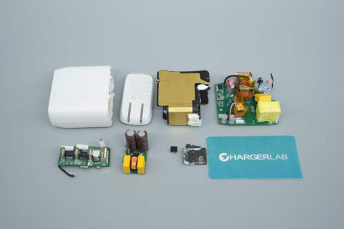
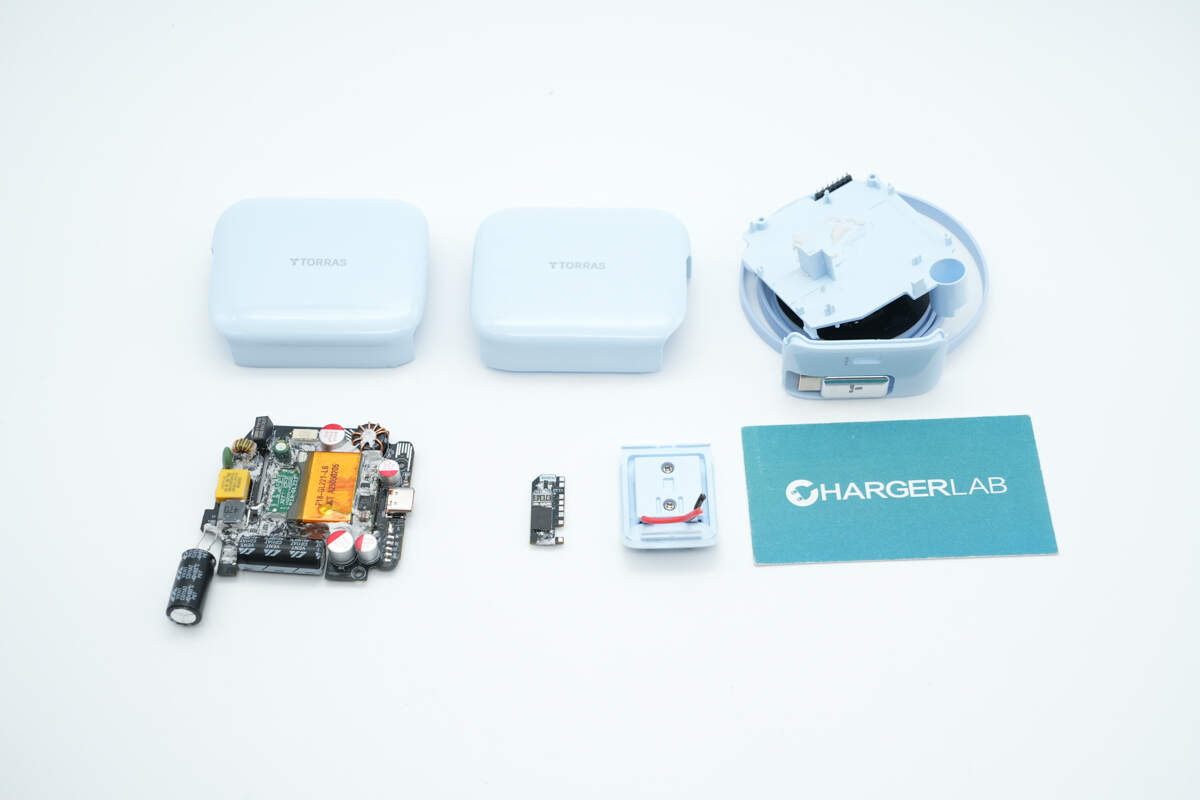
After disassembling the housing, the prong module is connected to the PCBA module via wires.
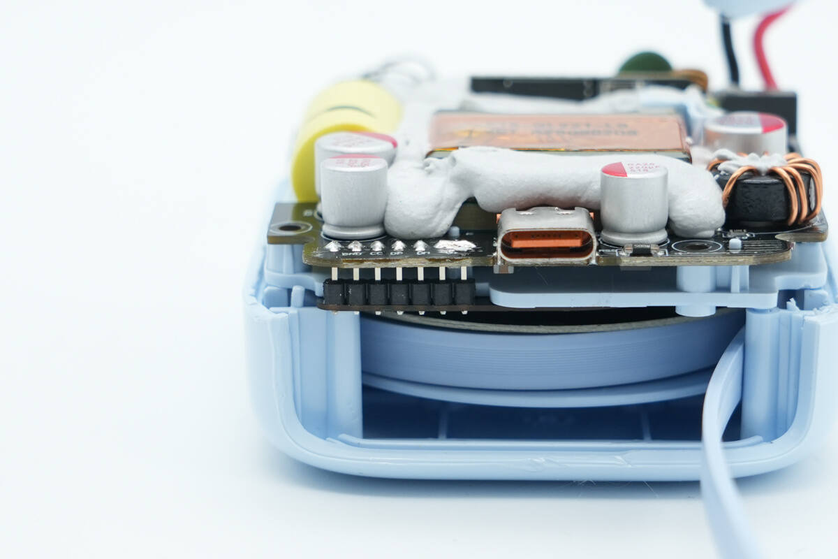
The retractable cable module is located at the bottom of the PCBA module, and the two are connected via pin headers.
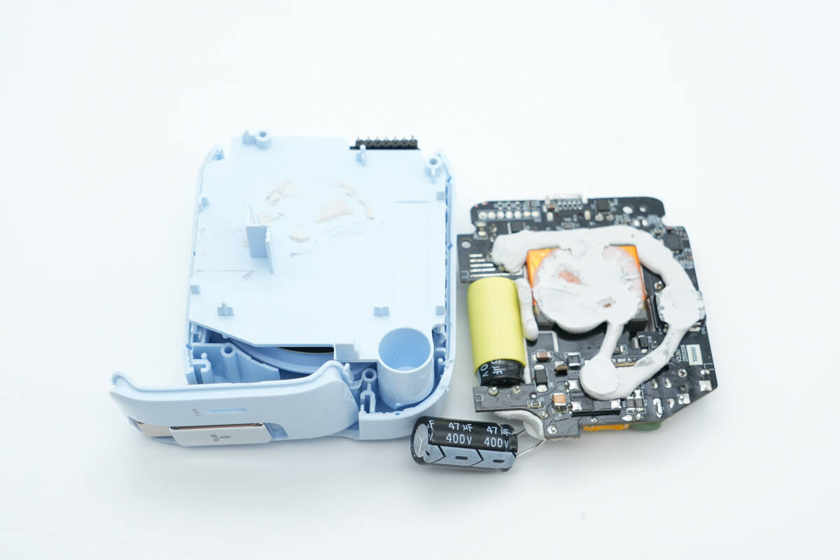
Remove the PCBA module; a plastic insulating plate is at the bottom.

The retractable cable module is also removed.
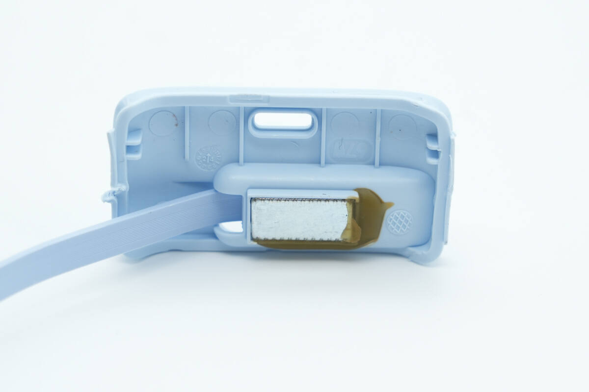
A magnet is installed on the inner side of the end housing and secured with adhesive.

The length of the PCBA module is about 60.51 mm (2.38 inches).
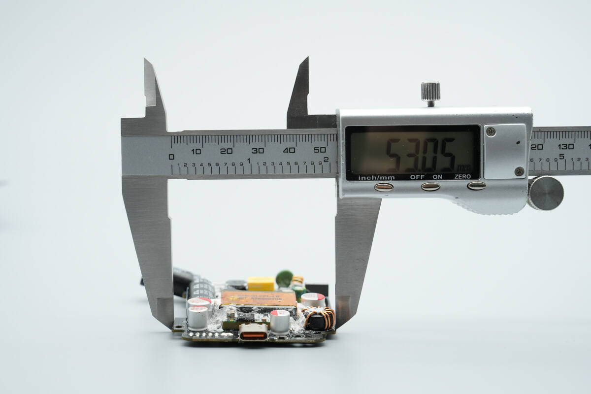
The width is about 53.05 mm (2.089 inches).
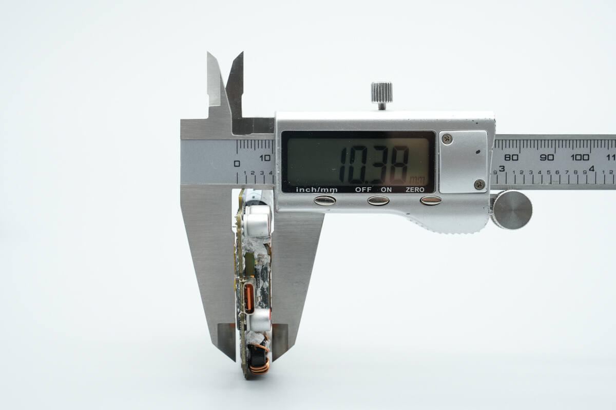
The thickness is about 10.38 mm (0.41 inches).

The front side of the PCBA module is extensively filled with thermal adhesive.
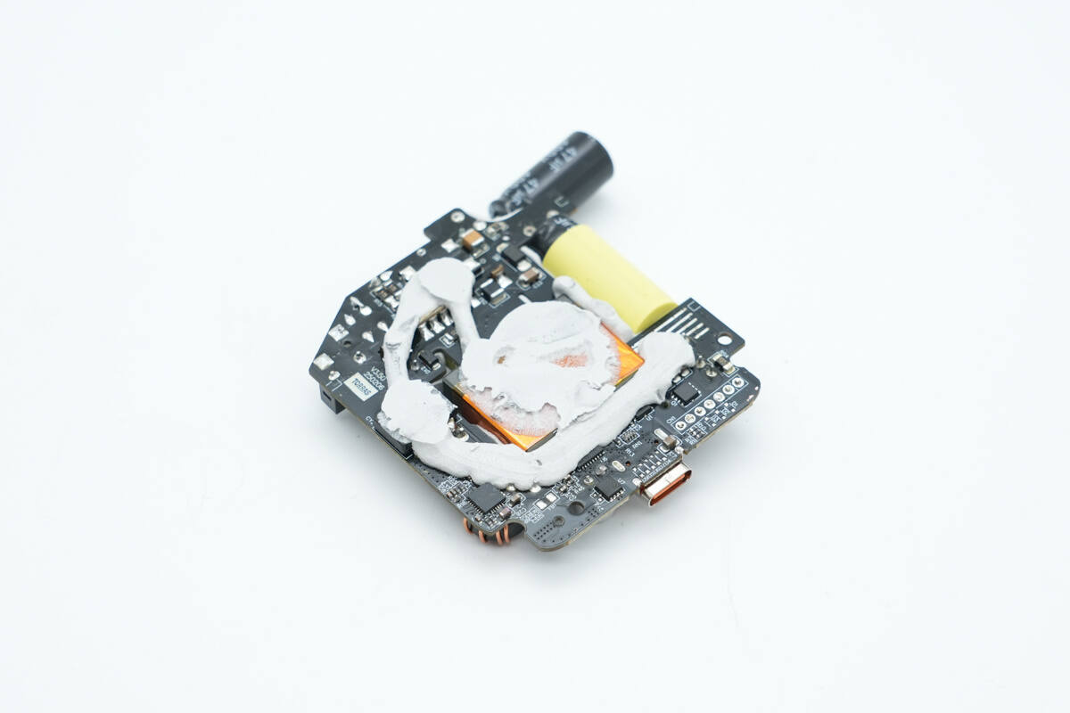
The rear side is also treated with adhesive, and the transformer adopts a low-profile planar design.
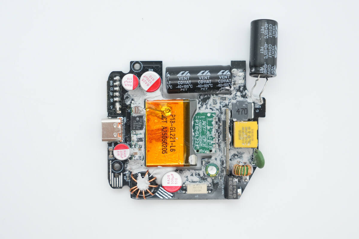
Remove the thermal adhesive. The front side of the module includes a small power PCB and a planar transformer module, along with components such as a time-delay fuse, common mode choke, capacitors, an optocoupler, and inductors.
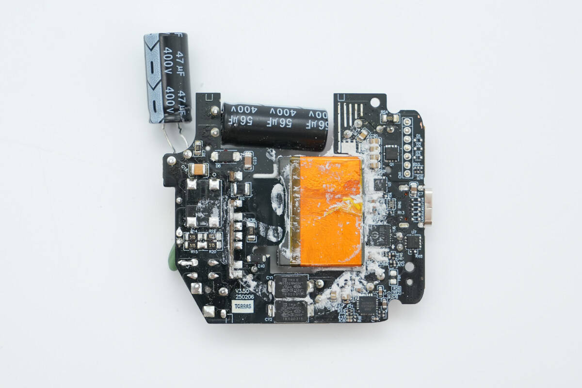
The rear side includes a bridge rectifier, SMD Y capacitors, a synchronous buck-boost converter, a protocol chip, and VBUS MOSFETs.
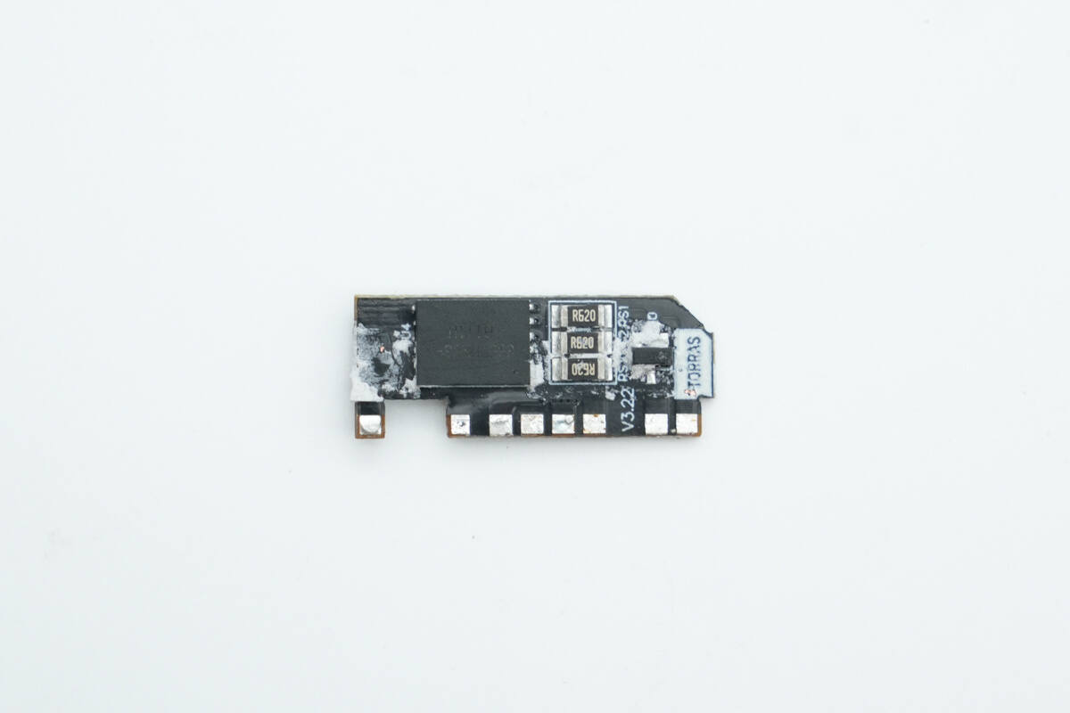
Remove the small PCB; the master control chip is on the front side.
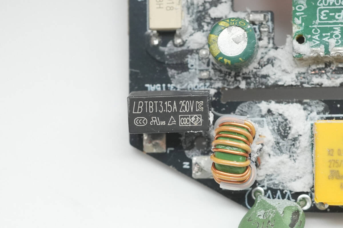
The time-delay fuse is from Lanbao and is rated at 3.15A 250V.
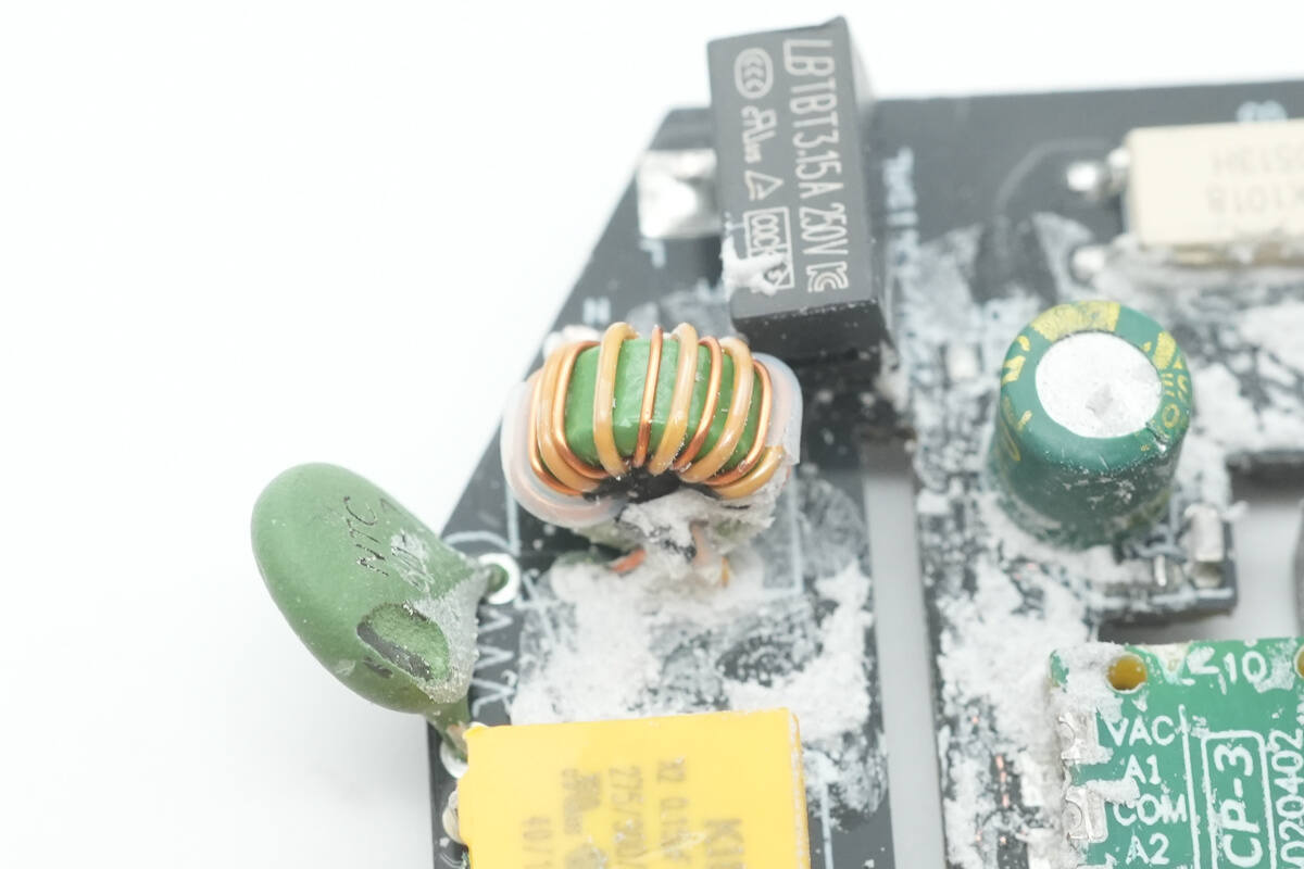
The common mode choke is used to suppress EMI.
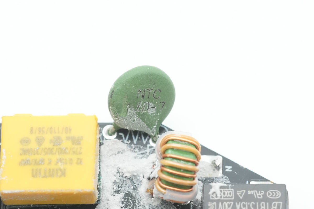
The NTC thermistor is used to suppress inrush current during power-on.
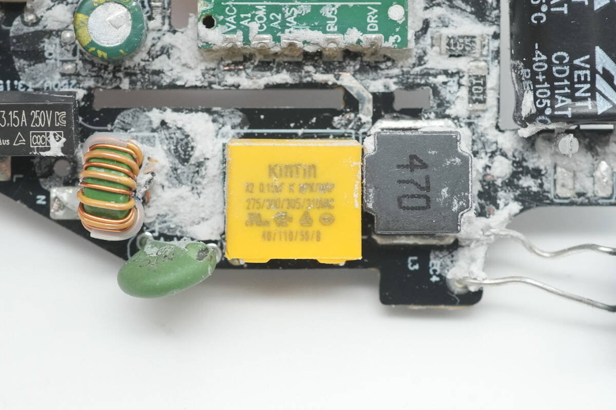
The safety X2 capacitor is from KinTin and has a capacitance of 0.15μF.
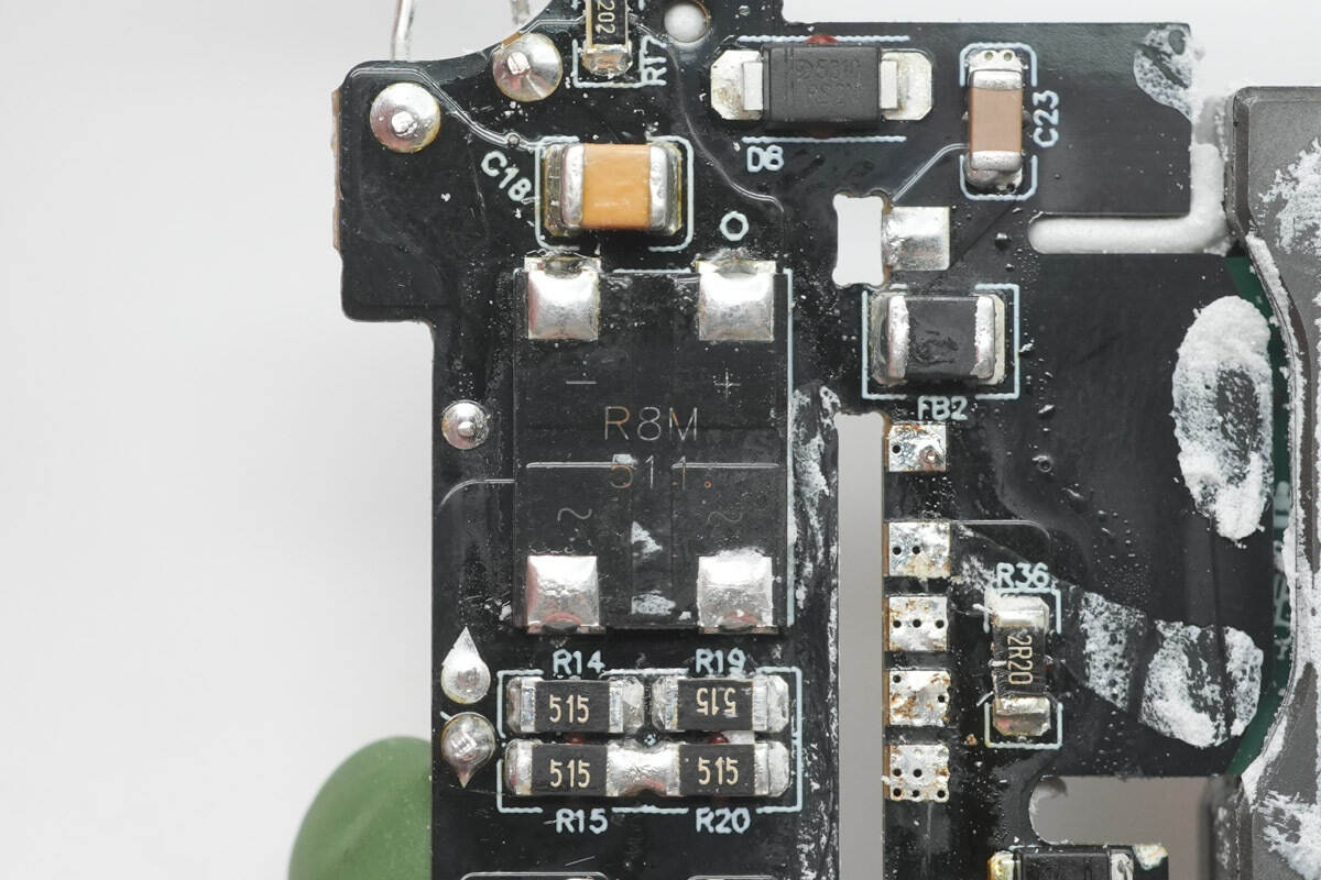
The bridge rectifier marked “R8M” is from ZOWIE.
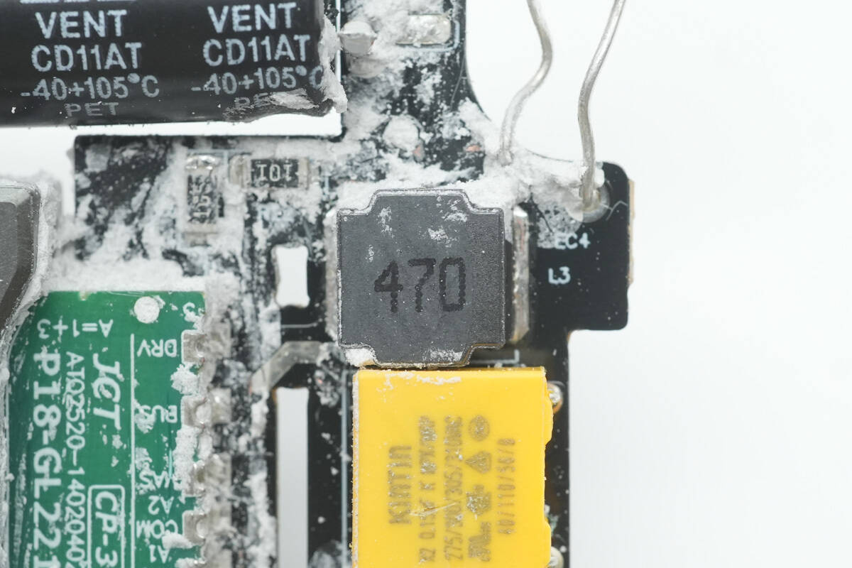
Close-up of the I-shaped inductor.
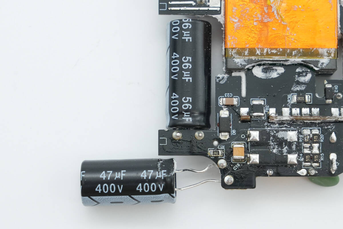
Two high-voltage filter electrolytic capacitors are from ChuangHui, rated at 400V 47μF and 400V 56μF, respectively.
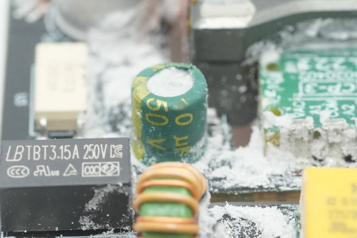
The capacitor supplying power to the master control chip is also from ChuangHui and is rated at 50V 10μF.
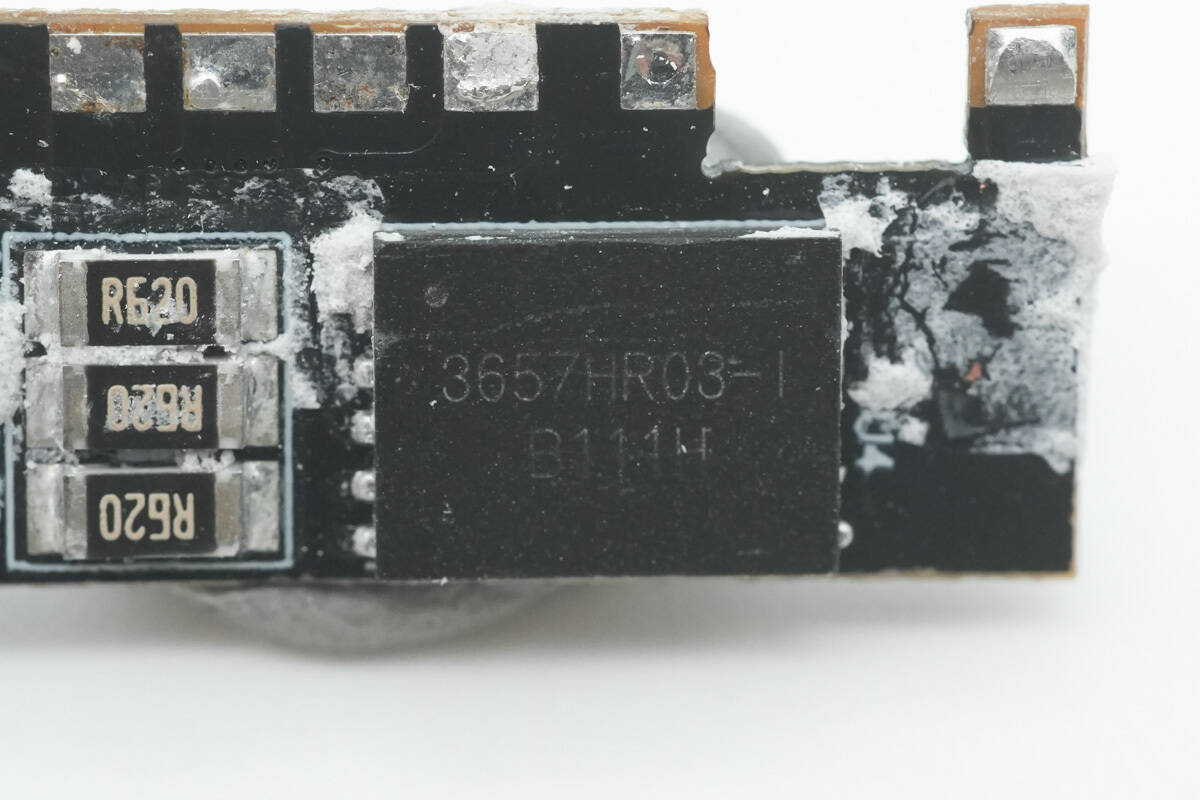
The GaN IC is from HYASiC, model HYC3657. It is an intelligent digital multi-mode flyback converter integrating a 700V enhancement-mode gallium nitride power device. The chip features a built-in 700V high-voltage startup circuit and adopts intelligent digital multi-mode control technology, enabling efficient operation based on peak current mode in burst mode, PFM, DCM, and quasi-resonant (QR) modes.
The HYC3657 optimizes EMI performance through switching frequency jittering technology and combines this with an adaptive GaN gate driver to achieve an optimal balance between switching losses and EMI performance. The chip integrates comprehensive protection functions, including output overvoltage protection, transformer saturation protection, VCC overvoltage protection, overload protection, input undervoltage/overvoltage protection, overtemperature protection, and line voltage feedforward compensation, ensuring high system reliability. The standby power consumption is below 20mW, and the device is provided in a DFN6x8 package.
The planar transformer is wrapped with copper foil and insulating tape.
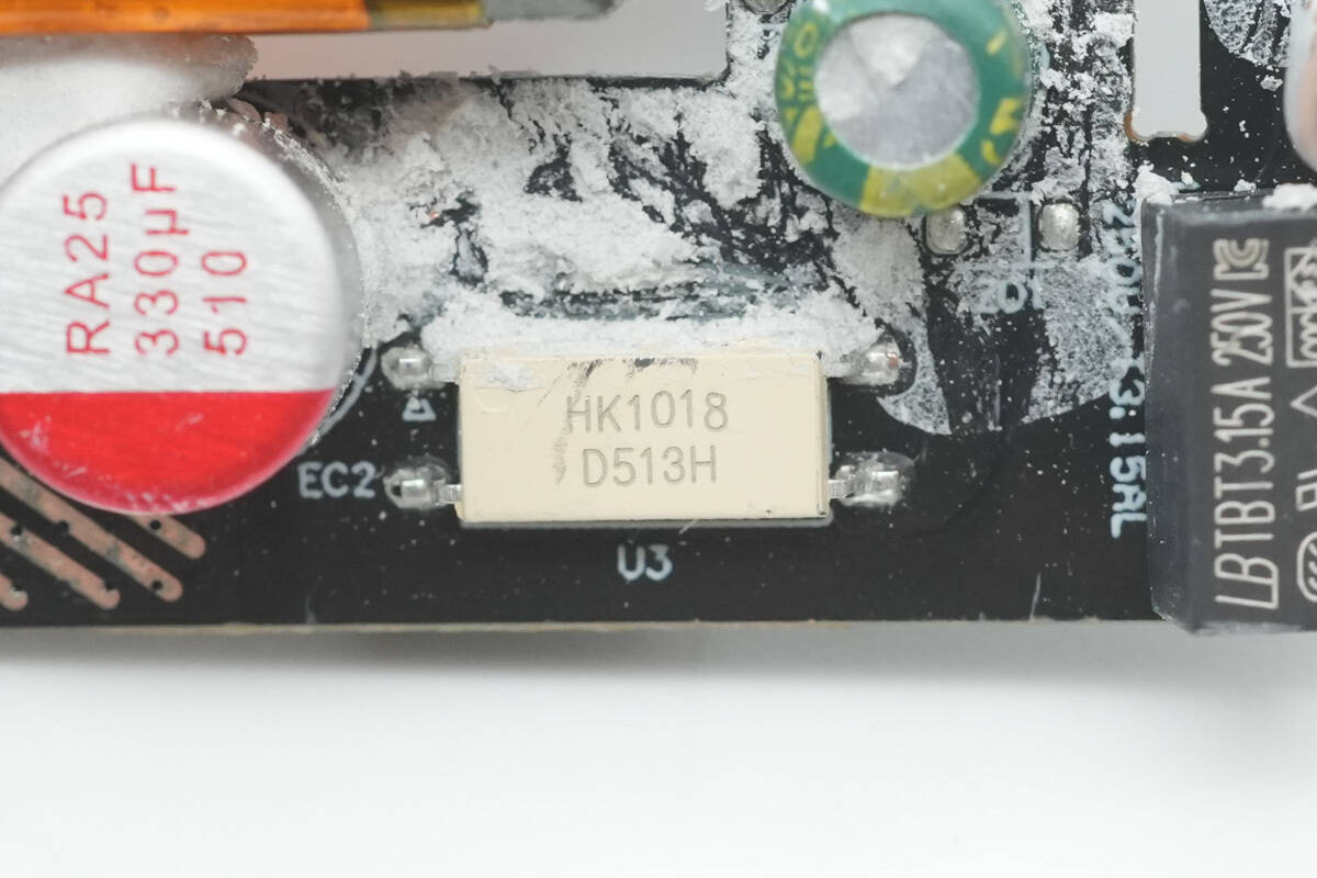
The HK1018 optocoupler is used for output voltage feedback.
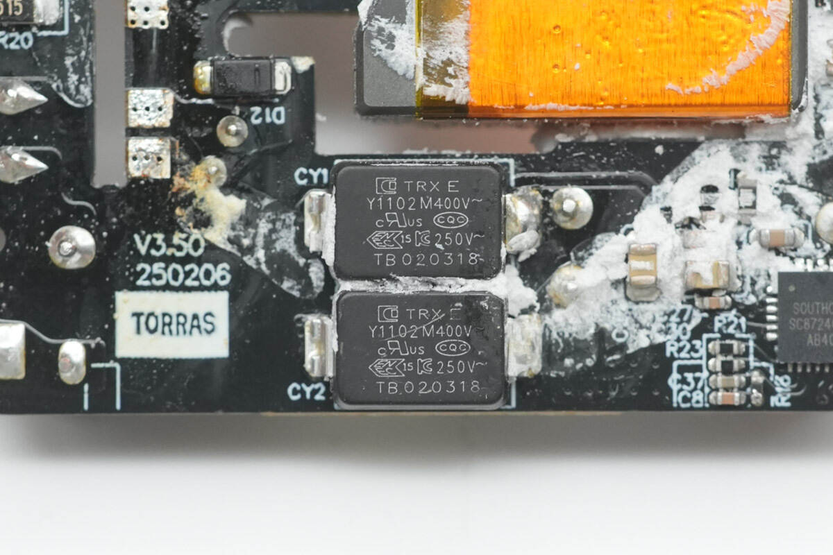
The SMD Y capacitors are from TRX. Their compact size and light weight make them well-suited for high-density power products such as GaN fast chargers. The part number is TMY1102M.
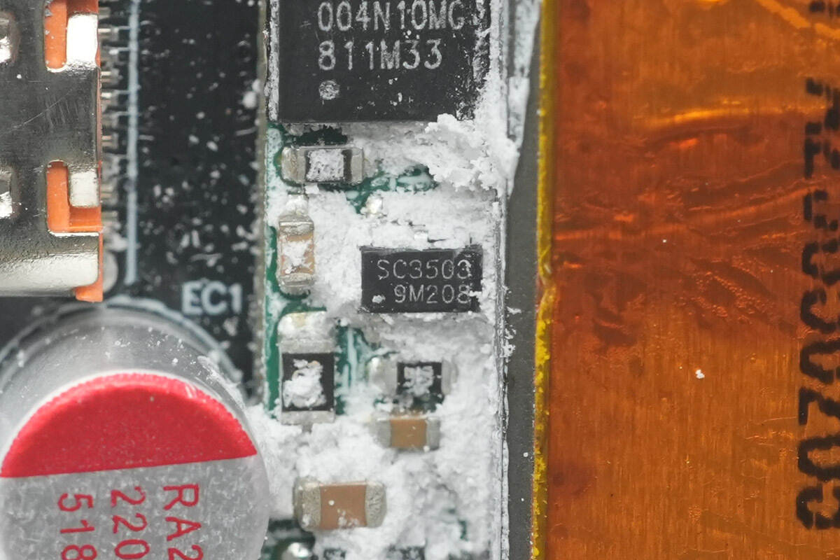
The synchronous rectifier controller is from SouthChip, model SC3503. It supports adaptive turn-on detection and fast turn-off, does not require an auxiliary winding for power supply, and allows the output voltage to drop as low as 0V. Its patented adaptive turn-on detection circuit prevents false turn-on of the synchronous rectification MOSFETs and is compatible with a wide range of MOSFETs. The controller features ultra-low quiescent current, supports multiple operating modes, and enables both high-side and low-side synchronous rectification with a highly simplified peripheral component count.
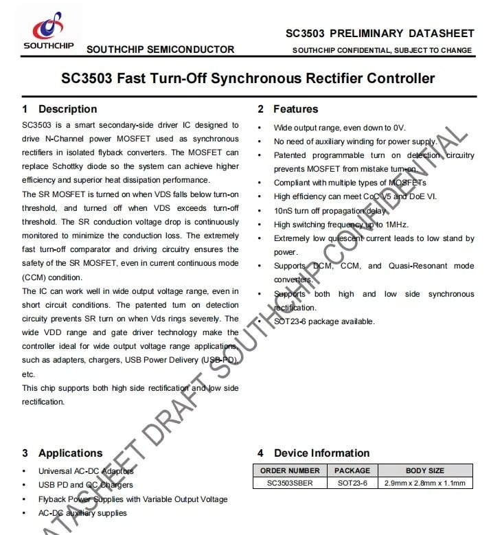
Here is the information about SouthChip SC3503.
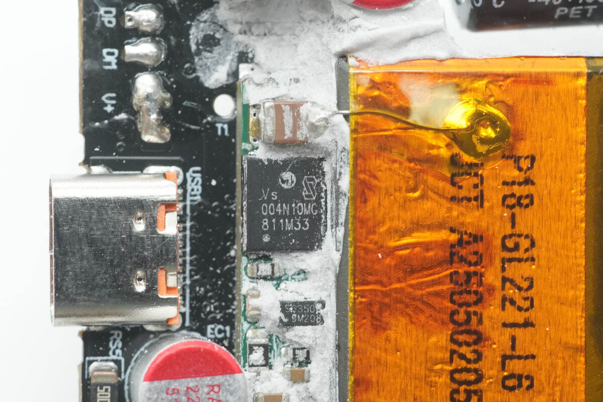
The synchronous rectifier is from Vergiga, model VSP004N10MS-G. It is rated at 100V, features an on-resistance of 3.8mΩ, and is packaged in a PDFN5060X form factor.
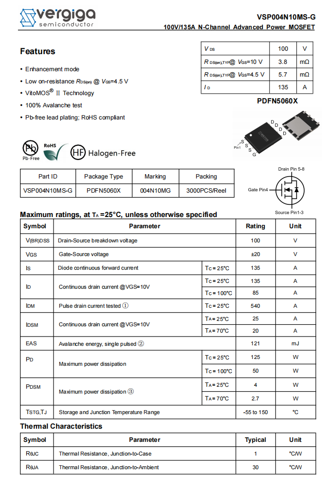
Here is the information about Vergiga VSP004N10MS-G.
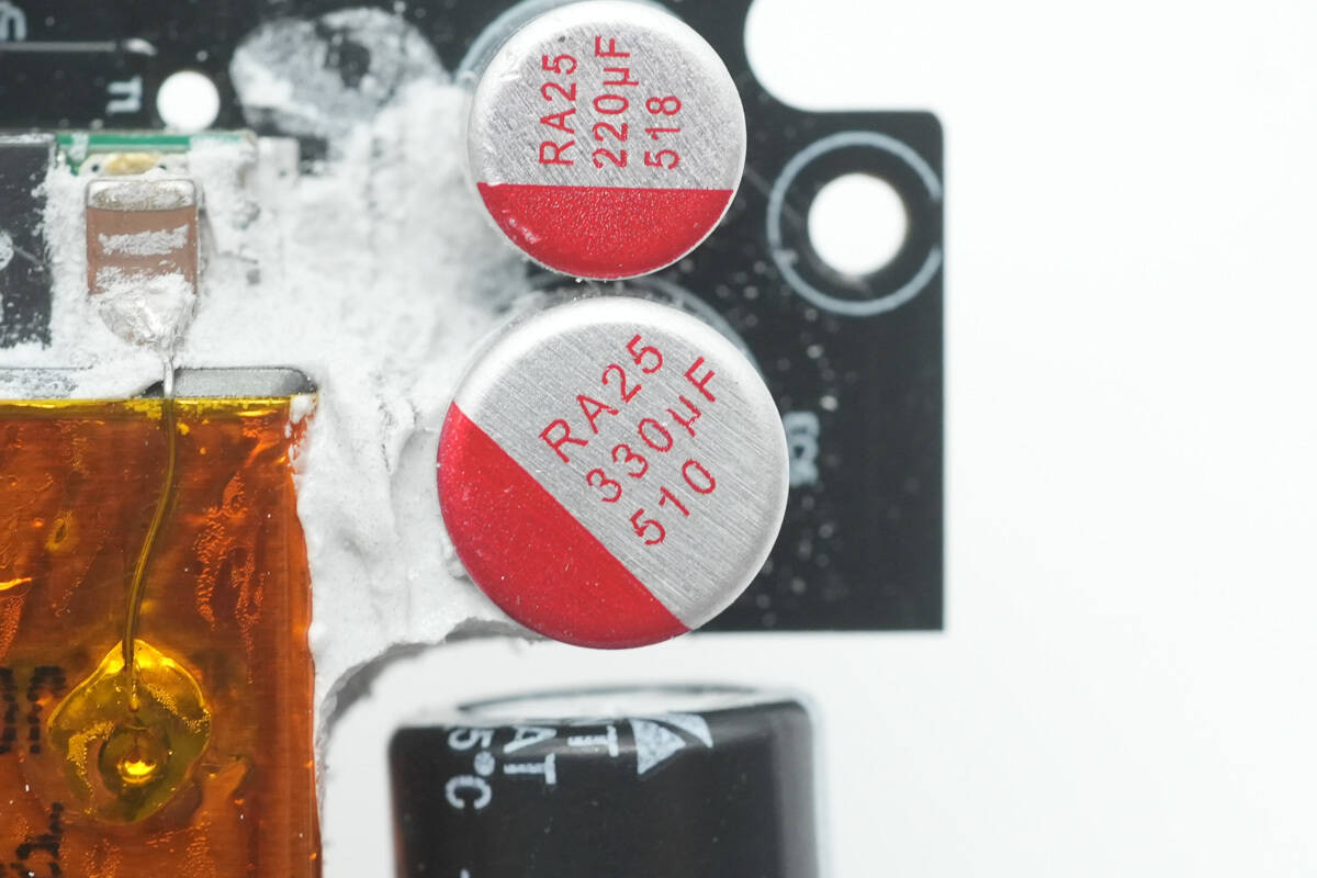
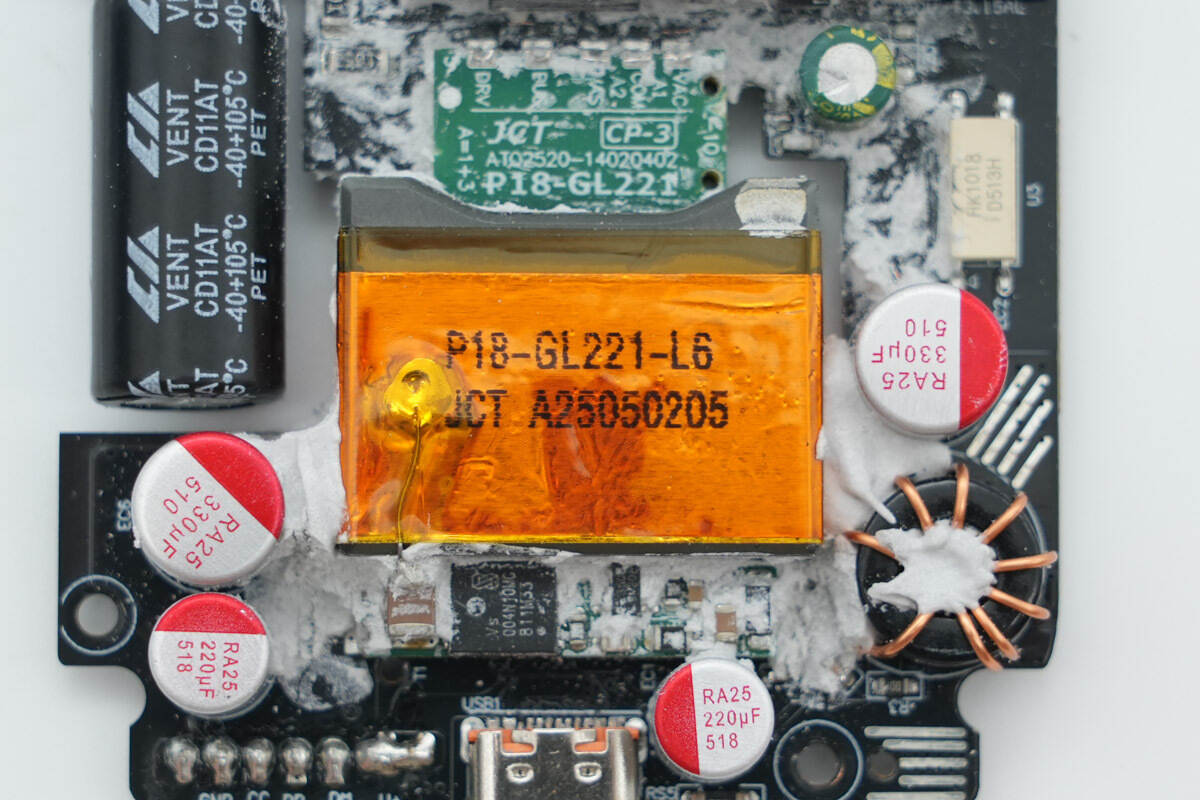
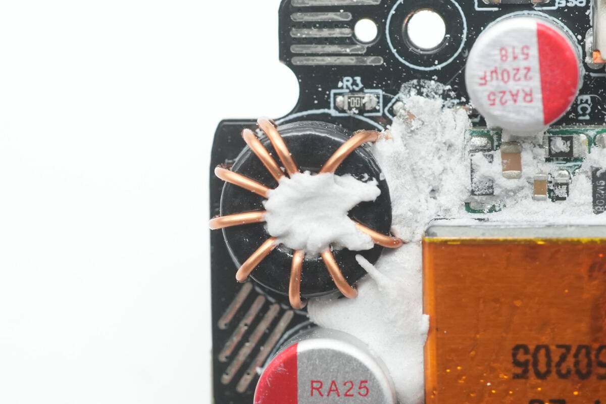
The solid capacitor for output filtering is rated at 25V330μF.
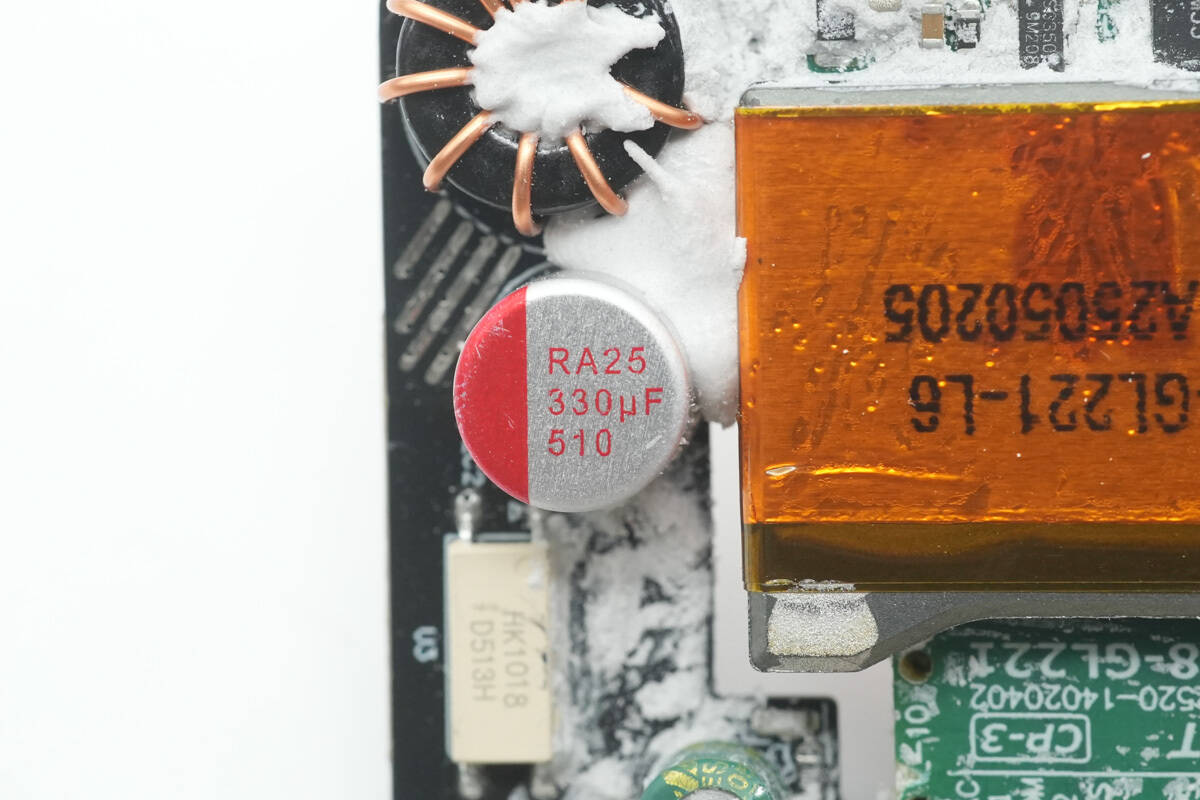
The other capacitor is rated at 25V220μF.
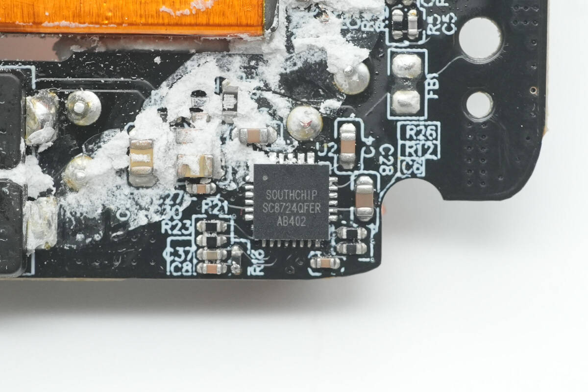
The synchronous buck-boost converter is from SouthChip, model SC8724. It integrates a four-MOS topology and delivers high efficiency and stable voltage regulation whether the output voltage is higher than, lower than, or equal to the input voltage. The SC8724 supports an input voltage range of 2.7V to 22V, an output voltage range of 3V to 22V, and a maximum output current of 3.5A.
The SC8724 adopts average current mode control. The output voltage is regulated by resistors connected to the FB pin. The operating mode (PSM/FPWM) and switching frequency can be configured through external settings. The device also provides programmable output current limiting, offering flexibility for different applications.
The SC8724 supports internal current limiting, input undervoltage protection, output overvoltage protection, output short-circuit protection, FB short-circuit protection, and overtemperature protection, ensuring safe operation under various fault conditions. The device is packaged in a 25-pin 4x4 QFN form factor.
Close-up of the matched inductor.
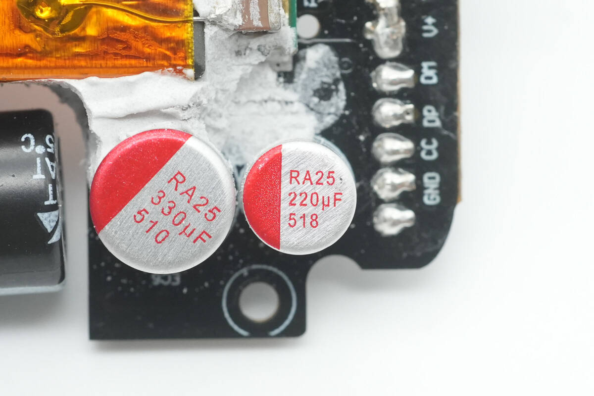
The secondary filtering solid capacitor is rated at 25V330μF.
The other one is rated at 25V220μF.
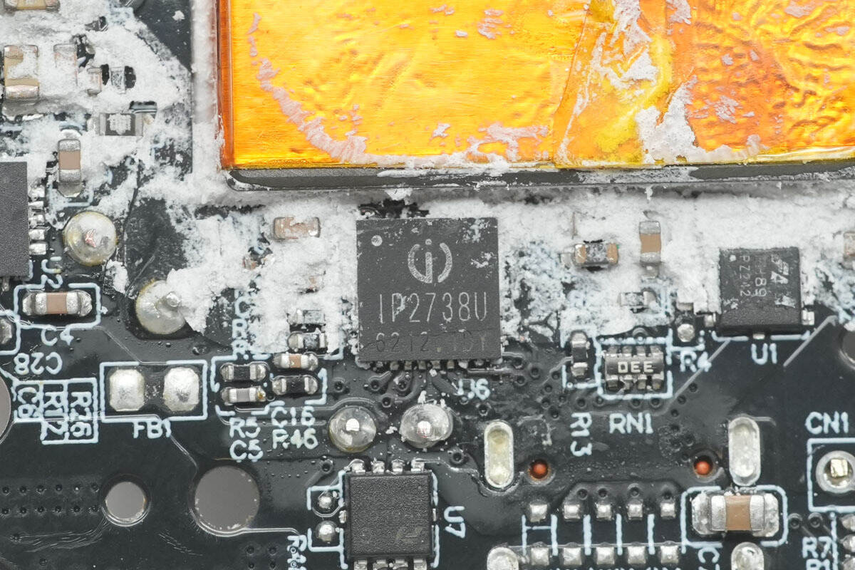
The protocol chip is from Injoinic, model IP2738U. It supports multiple USB ports and is designed for dual-port 18–140W fast-charging applications. The chip features independent feedback control and independent USB PD control, effectively integrating the functionality of two IP2736 devices into a single chip, with fast-charging specifications identical to those of the IP2736. It supports USB PD3.1 28V EPR profiles, as well as a wide range of fast-charging protocols, including PD3.0 and PPS, offering excellent compatibility.
The Injoinic IP2738U integrates four independent NMOS gate drivers, which can be used for multi-port output control. These drivers control multiple VBUS MOSFETs for output port switching and dual power path paralleling. In addition, the chip supports dual independent overcurrent, overvoltage, and short-circuit protection, ensuring safe operation.
Here is the information about Injoinic IP2738U.
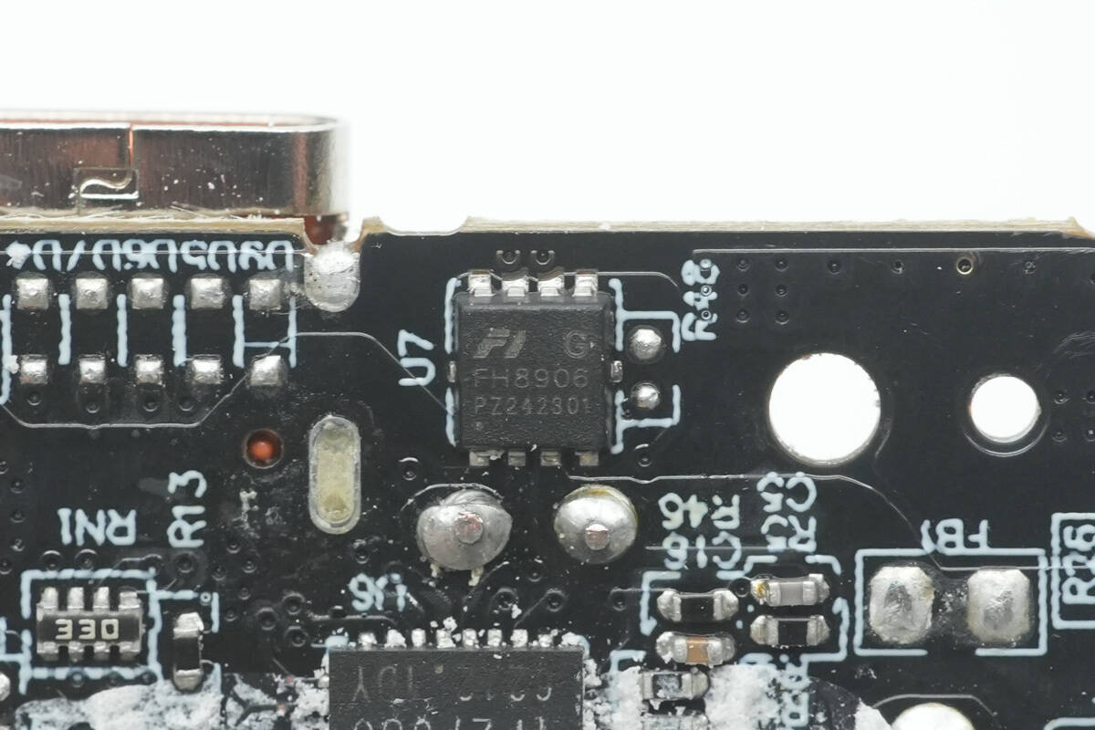
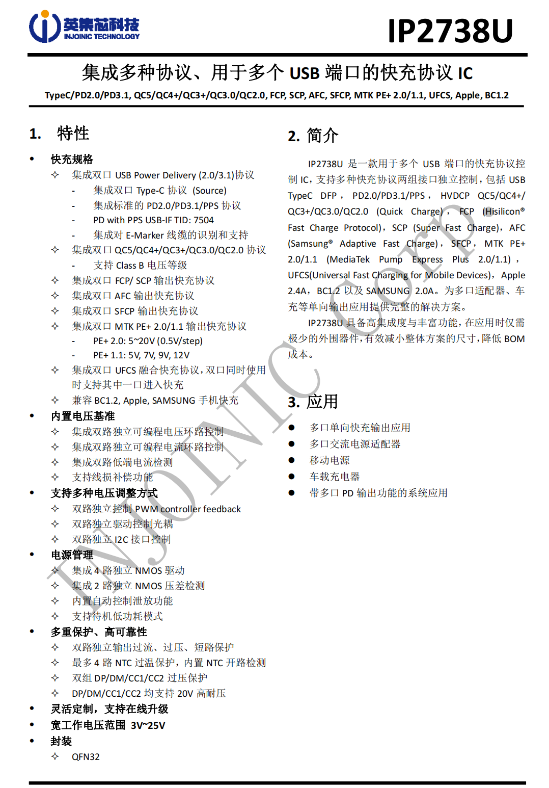
The VBUS MOSFET is from Xinfeihong, model FH8906G6. It is a dual NMOS device rated at 30V with an on-resistance of 6.5mΩ, and it is packaged in a PDFN3.3×3.3-8L form factor.
The other VBUS MOSFET also uses the Xinfeihong FH8906G6.
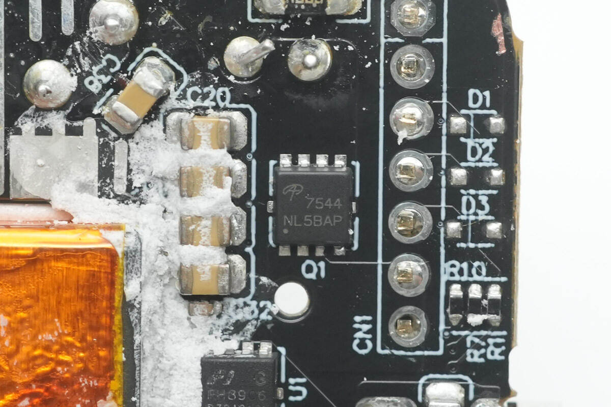
Another VBUS MOSFET is from AOS, model AON7544. It is an NMOS rated at 30V with an on-resistance of 4.1mΩ, packaged in a DFN3×3 form factor.
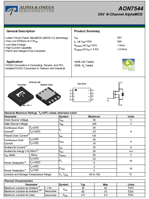
Here is the information about AOS AON7544.
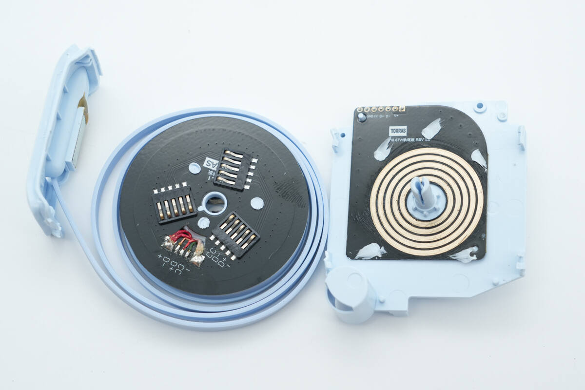
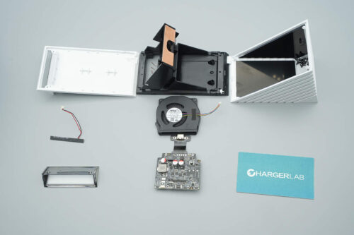
Overview after disassembling the retractable cable module.
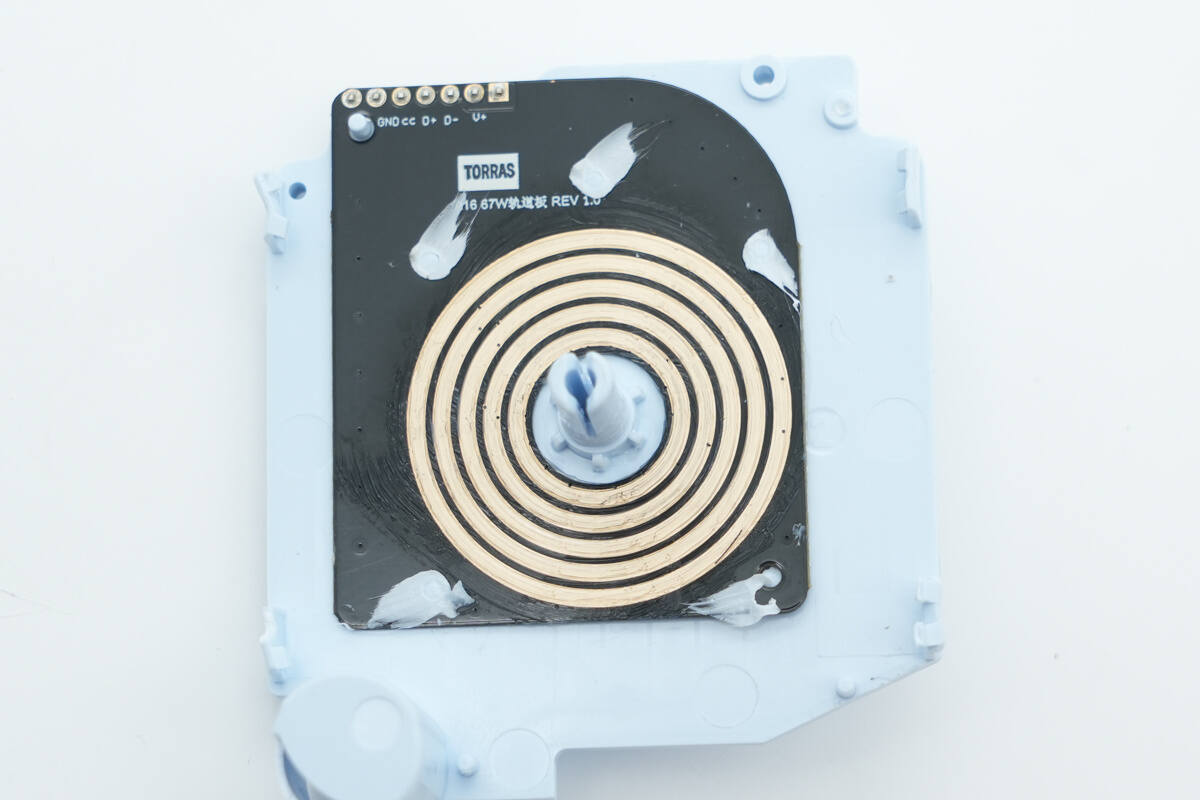
Close-up of the PCB slip ring.
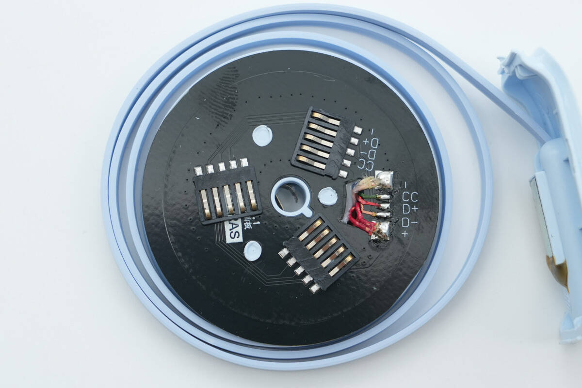
The retractable cable spool is equipped with three brushes to increase current-carrying capacity.
Well, those are all components of the Torras FlexLine 67W Charger.
Summary of ChargerLAB
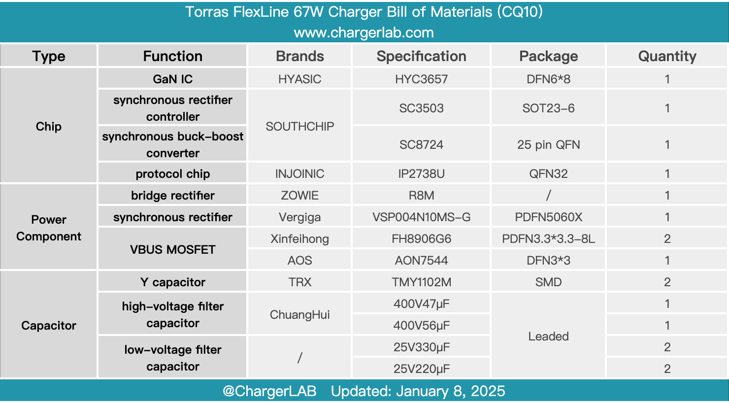
Here is the component list of the Torras FlexLine 67W Charger for your convenience.
It is equipped with a USB-C port and a retractable cable, both supporting a maximum output of 67W and compatible with protocols such as QC3.0, SCP, PD3.0, and PPS. Its performance and power distribution strategy meet current mainstream requirements, while the retractable cable provides excellent portability.
After taking it apart, we found that it uses a HYASiC HYC3657 GaN IC, with a SouthChip SC3503 synchronous rectifier controller on the secondary side. Secondary-side buck conversion is handled by the SouthChip SC8724, while the dual-port output is managed by the Injoinic IP2738U protocol chip. The internal structural design and thermal management are solid and reliable.
Related Articles:
1. Teardown of Anker Prime 150W Charging Station (A1903)
2. Teardown of Anker Prime 160W Charger with Smart Display (A2687)
3. Teardown of Anker Nano 75W Car Charger (A2738)