
Introduction
Last year, ChargerLAB performed a deep dive into a 60W single-port USB-C fast charger from Ruiyuan, which supported the PD3.2/AVS standard. It was one of those devices that nailed the trifecta of design, portability, and power.
Recently, our team got our hands on Ruiyuan’s latest 65W GaN PD fast charger. It retains the signature compact, square-box form factor of its predecessor but takes things a step further by incorporating foldable prongs, making it even more travel-friendly for your daily carry.
Under the hood, you’re looking at continued support for PD3.2 and 9-20V 3A SPR AVS, making this a go-to solution for topping off phones, tablets, and light laptops on the fly.
We've stripped the casing off to get a look at the internals—let's see if this one is as well-engineered as it looks.
Product Appearance
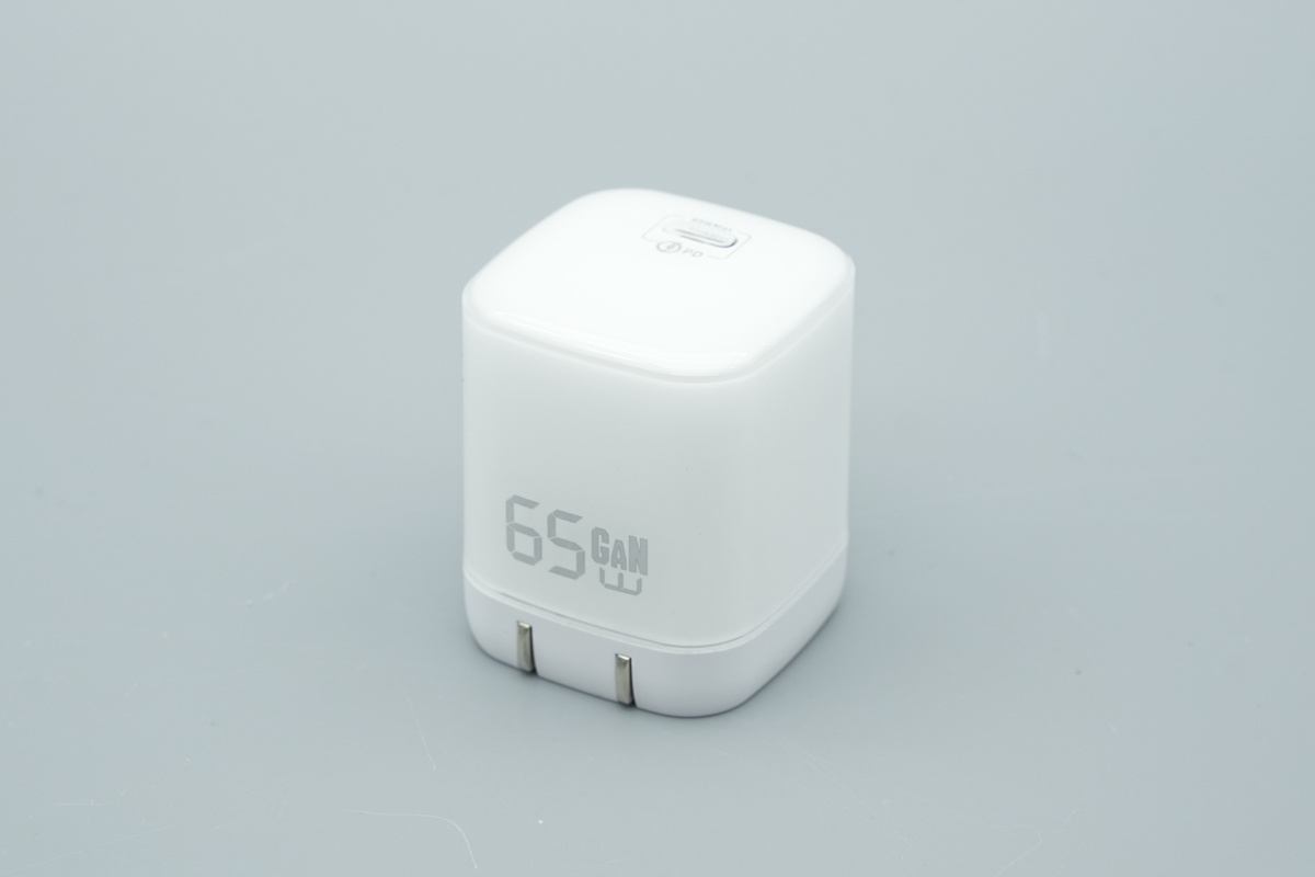
The 65W GaN charger features a square, white flame-retardant PC housing with a dual-texture design combining glossy and matte finishes.
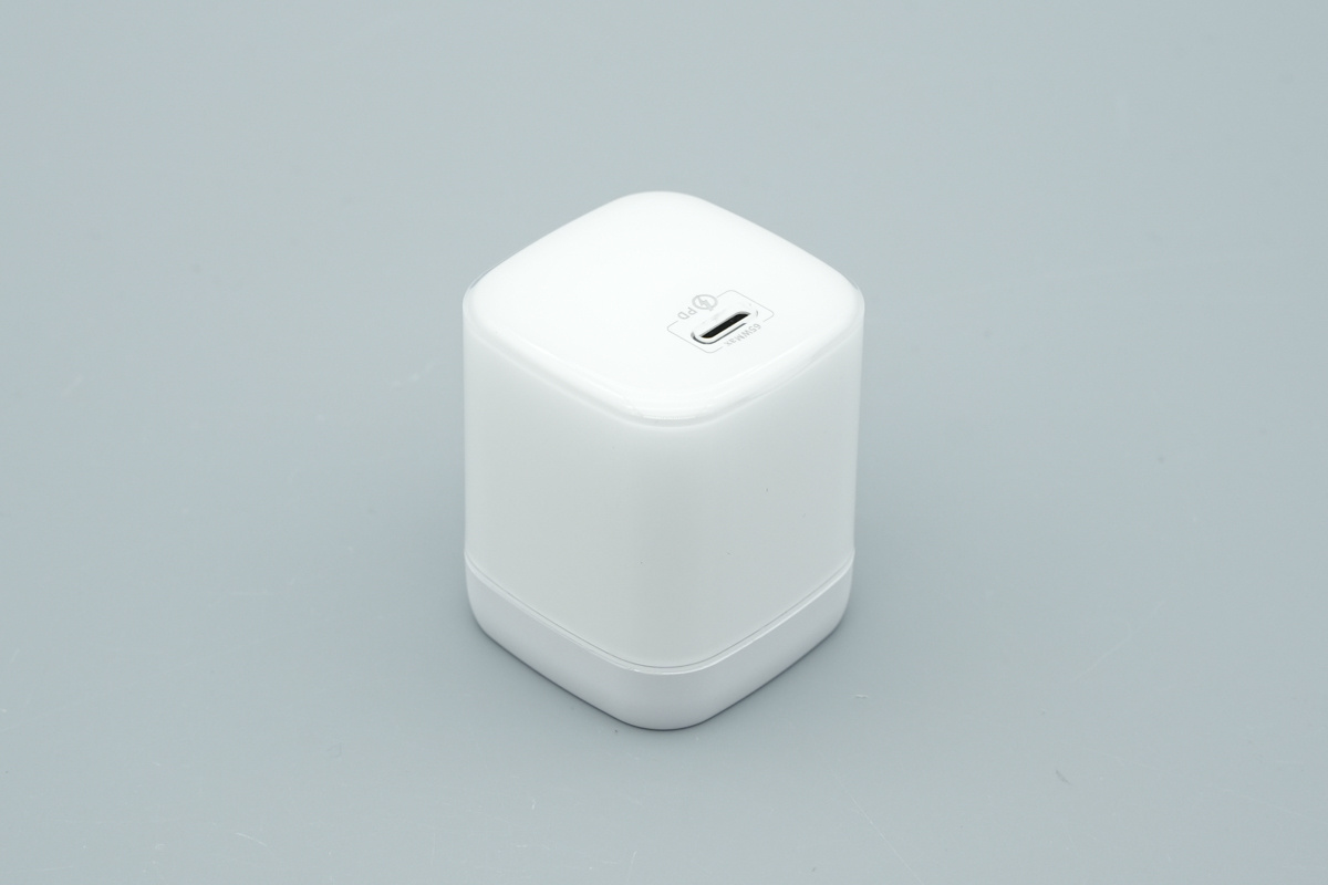
A single USB-C output port is located on the top panel, marked with '65W Max' and the PD fast-charging icon.
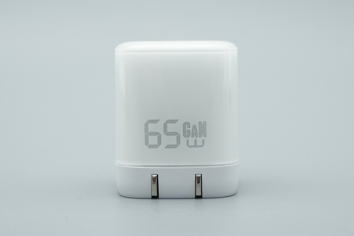
You’ll find '65W GaN' clearly printed on the side.
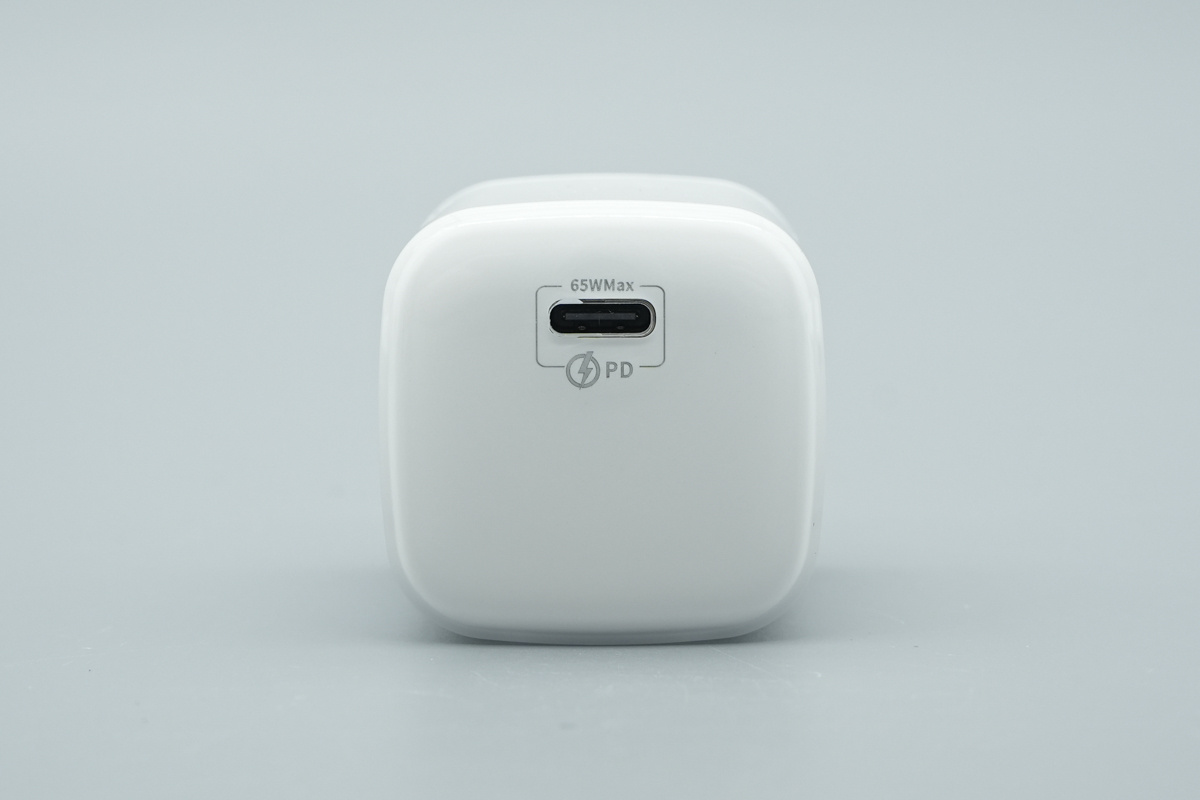
The top USB-C output port features a black plastic sheet inside.
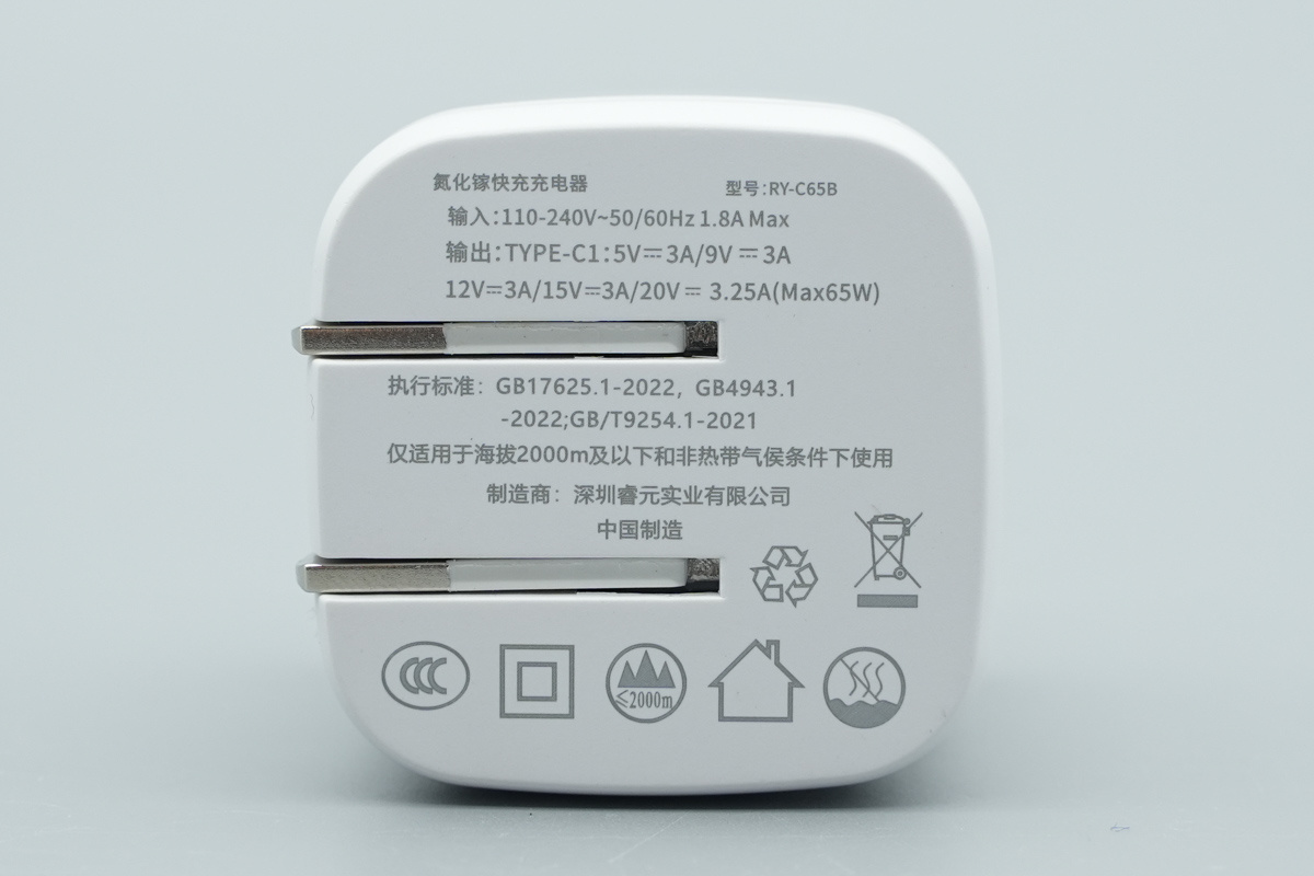
Product specs are printed on the base as follows:
Name: GaN Fast Charger
Model: RY-C65B
Input: 110-240V~50/60Hz, 1.8A Max
Output: 5V3A, 9V3A, 12V3A, 15V3A, 20V3.25A (65W Max)
Manufacturer: Shenzhen Ruiyuan Industrial Co., Ltd.
Certification: Made in China, Chinese CCC certified.
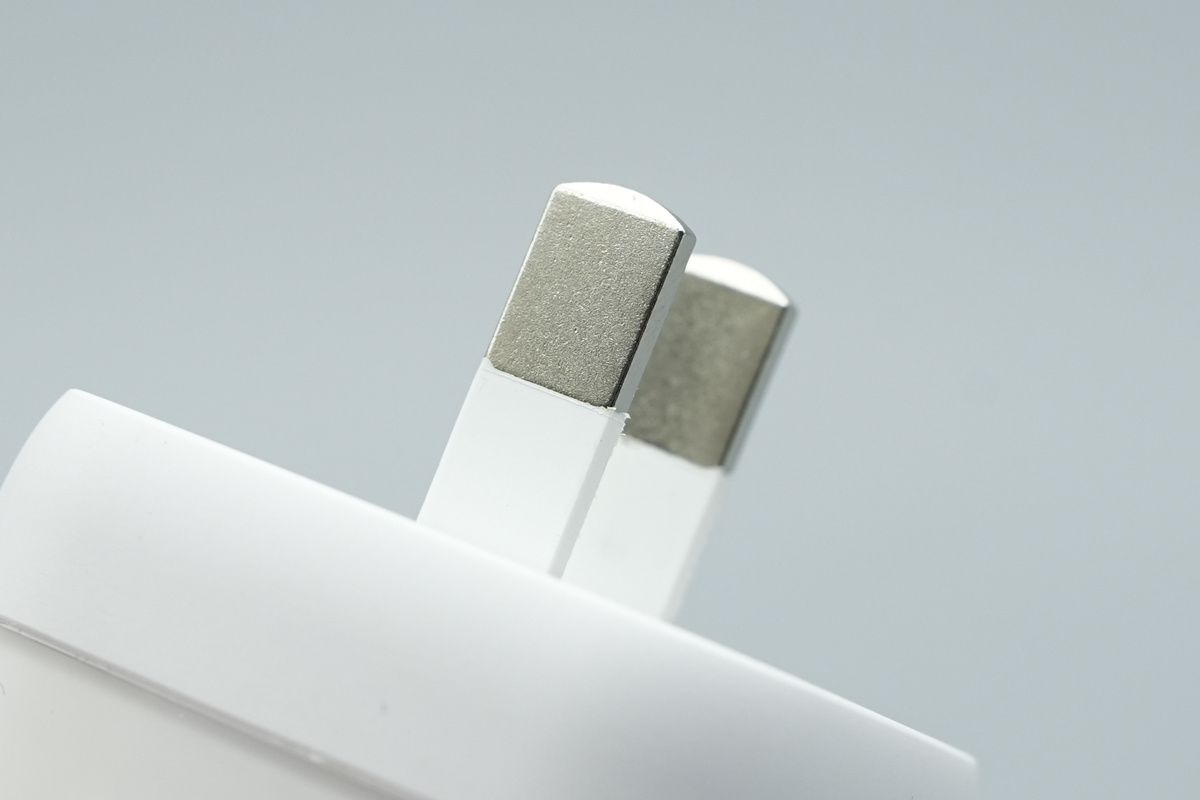
Featuring new Chinese standard foldable prongs, it can be easily stored without damaging other items, offering excellent portability for travel.
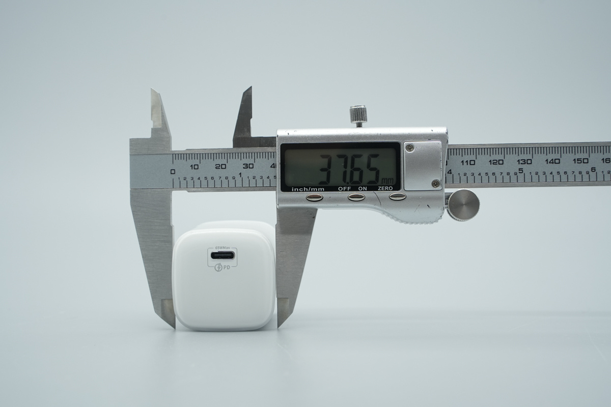
The length of the charger is about 37.65mm (1.482 inches).
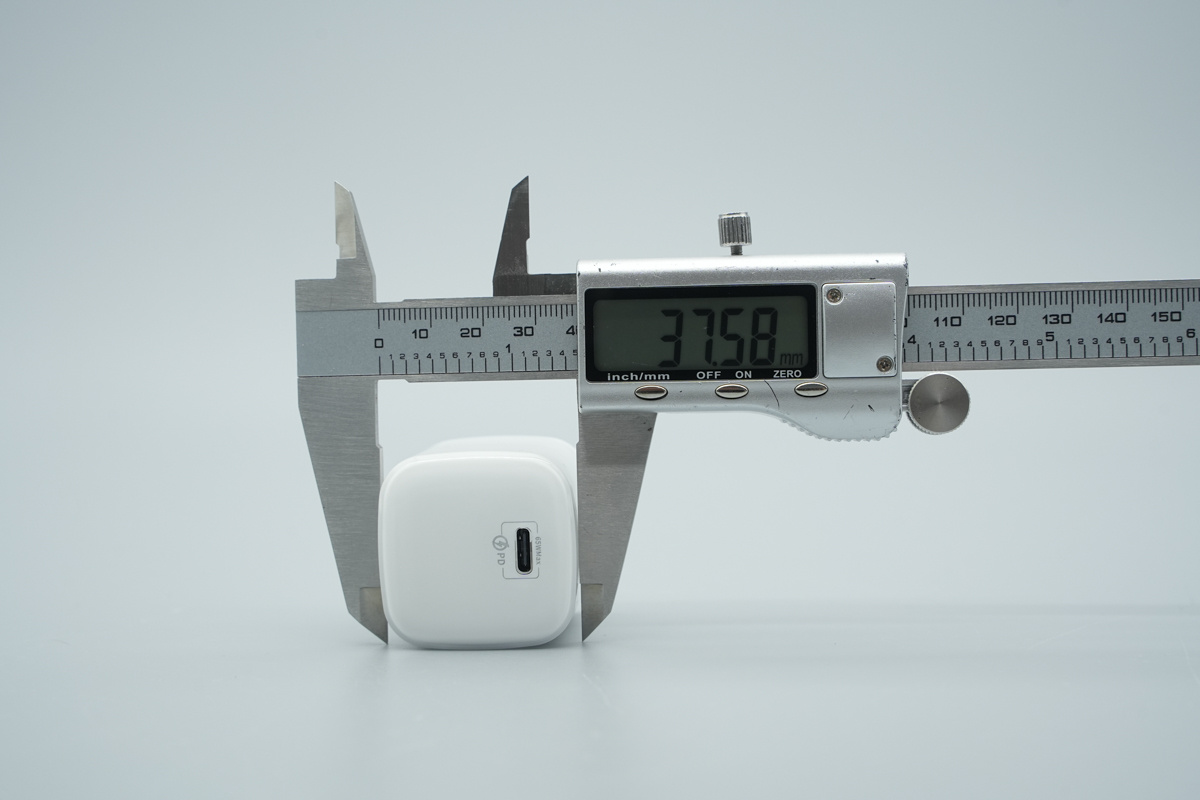
The width of the charger is about 37.58mm (1.480 inches).
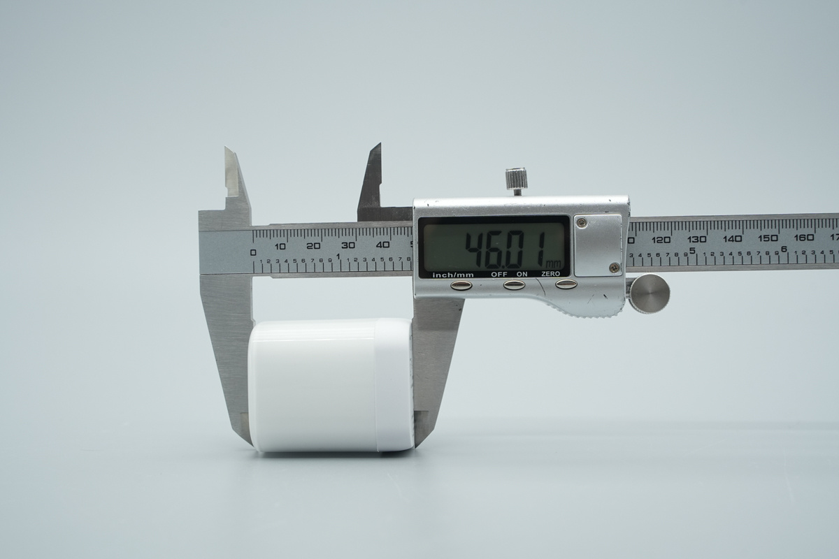
The height of the charger is about 46.01mm (1.811 inches).
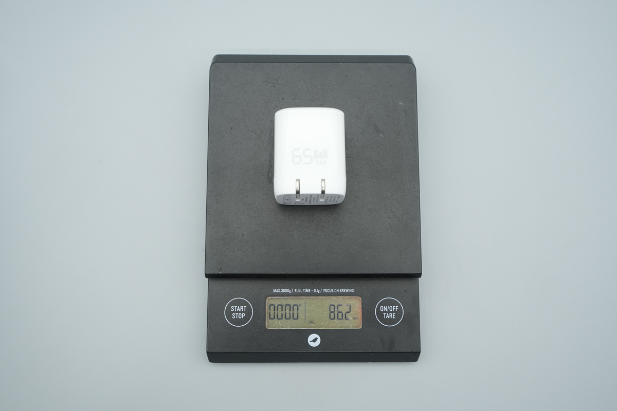
The weight is about 86.2g (3.04 oz).
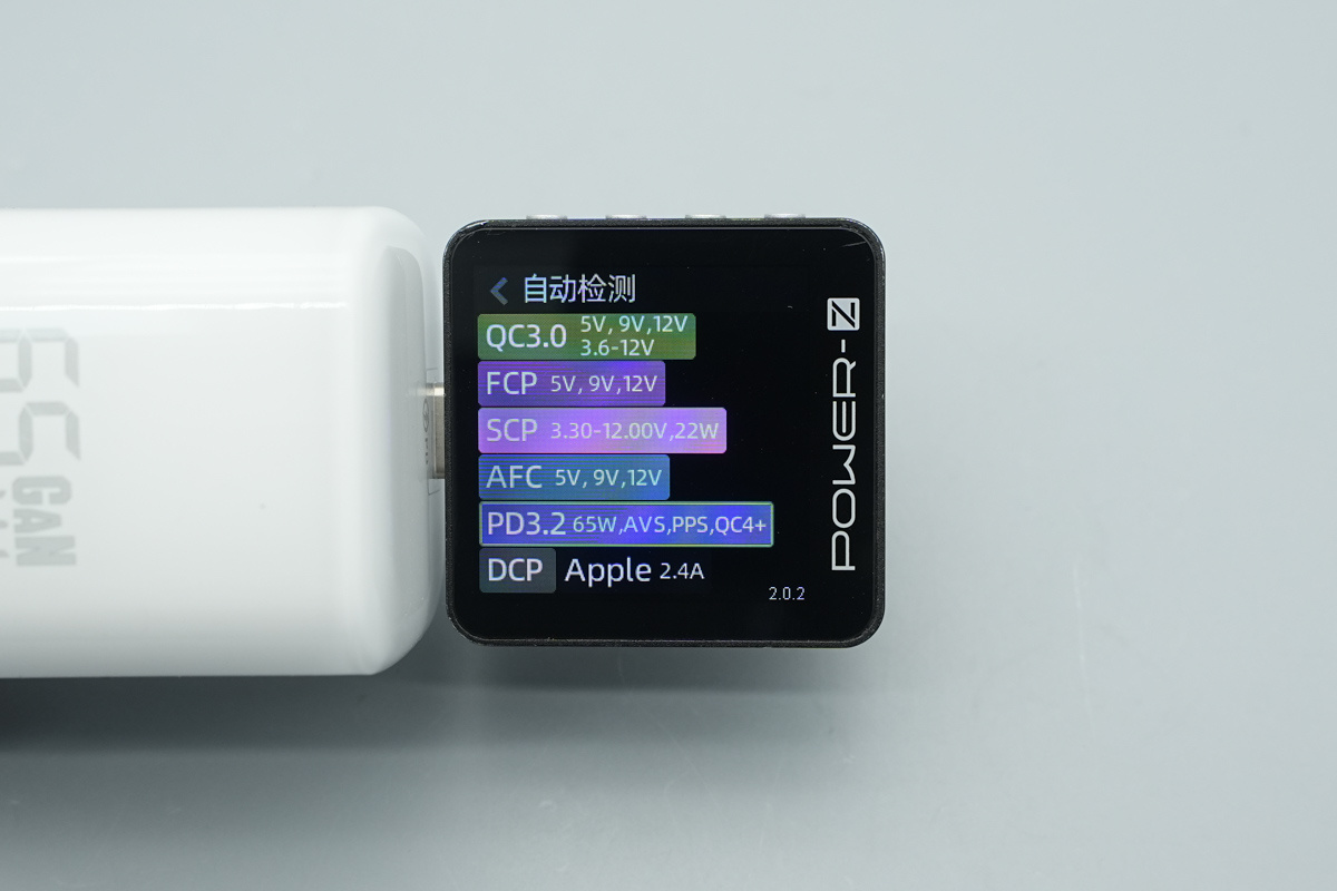
ChargerLAB POWER-Z KM003C shows that the USB-C port supports QC3.0, FCP, SCP, AFC, PD3.2/PPS/AVS, QC4+, Apple 2.4A and DCP.
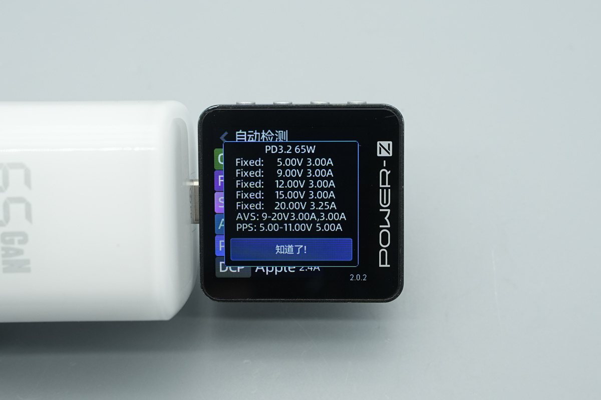
And it also supports five fixed PDOs of 5V3A, 9V3A, 12V3A, 15V3A and 20V3.25A, and features 9-20V 3.0A AVS subset, and features PPS subset: 5.00-11.00V 5.00A.
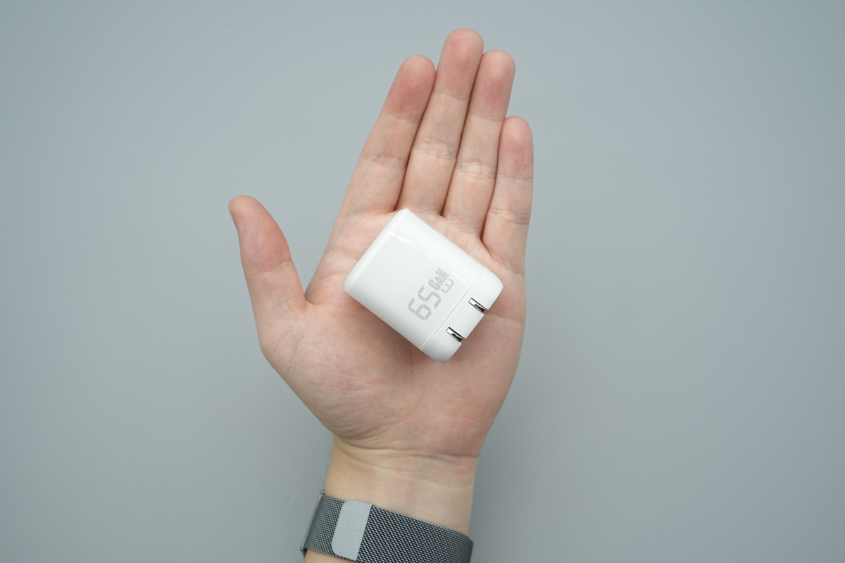
That's how big it is in the hand.
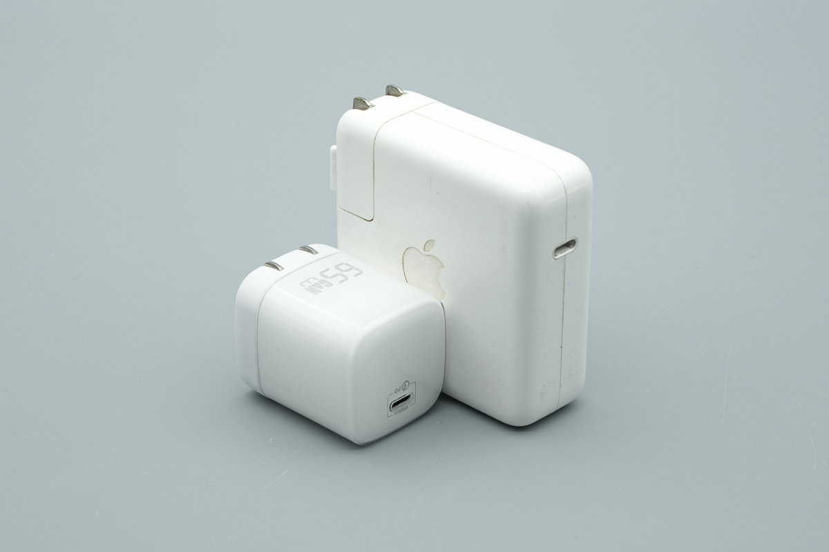
Put it with Apple’s 67W dynamic charger, it is remarkably smaller.
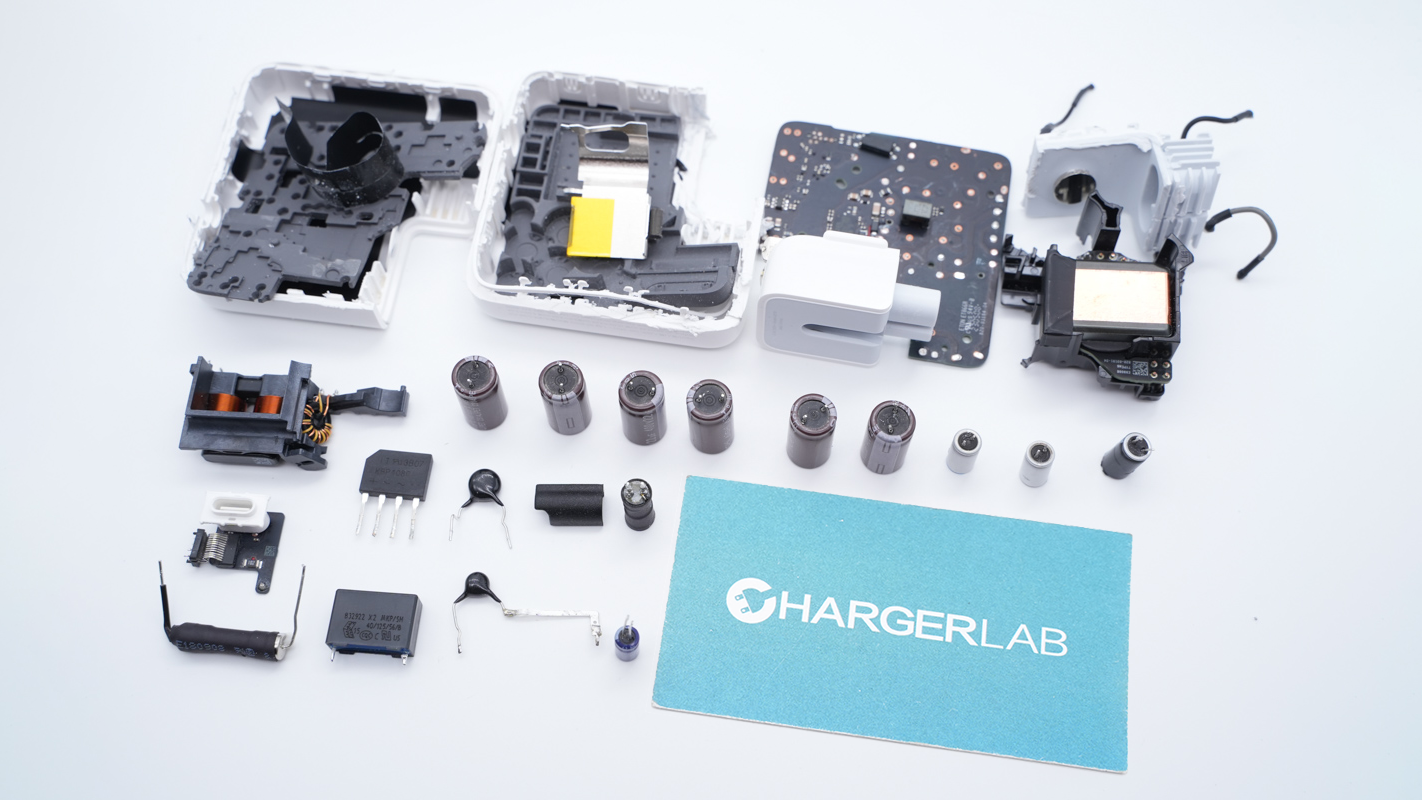
Following our assessment of the charger's design and protocol support, let’s dive into the teardown and see how this Ruiyuan charger is built.
Teardown
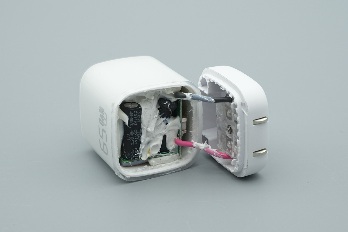
Opening the housing reveals a significant amount of white thermal potting compound. Red and black wires connect the foldable prongs to the PCBA.
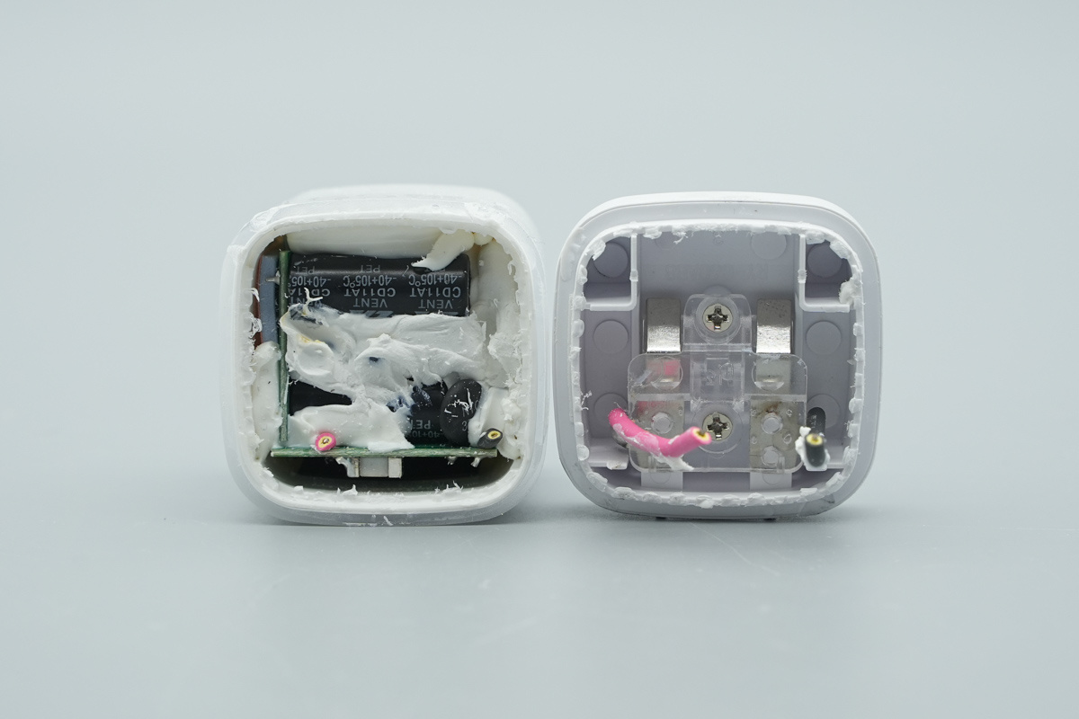
Next, removing the foldable prong assembly to get a clearer view of the input side.
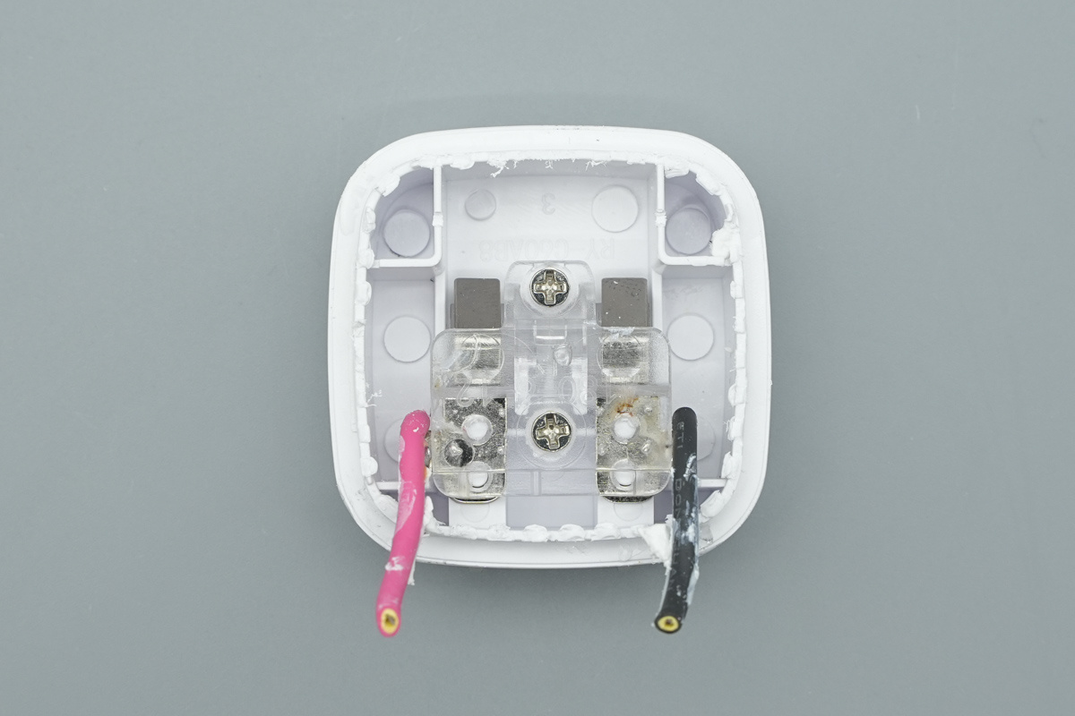
This is the foldable prong module.
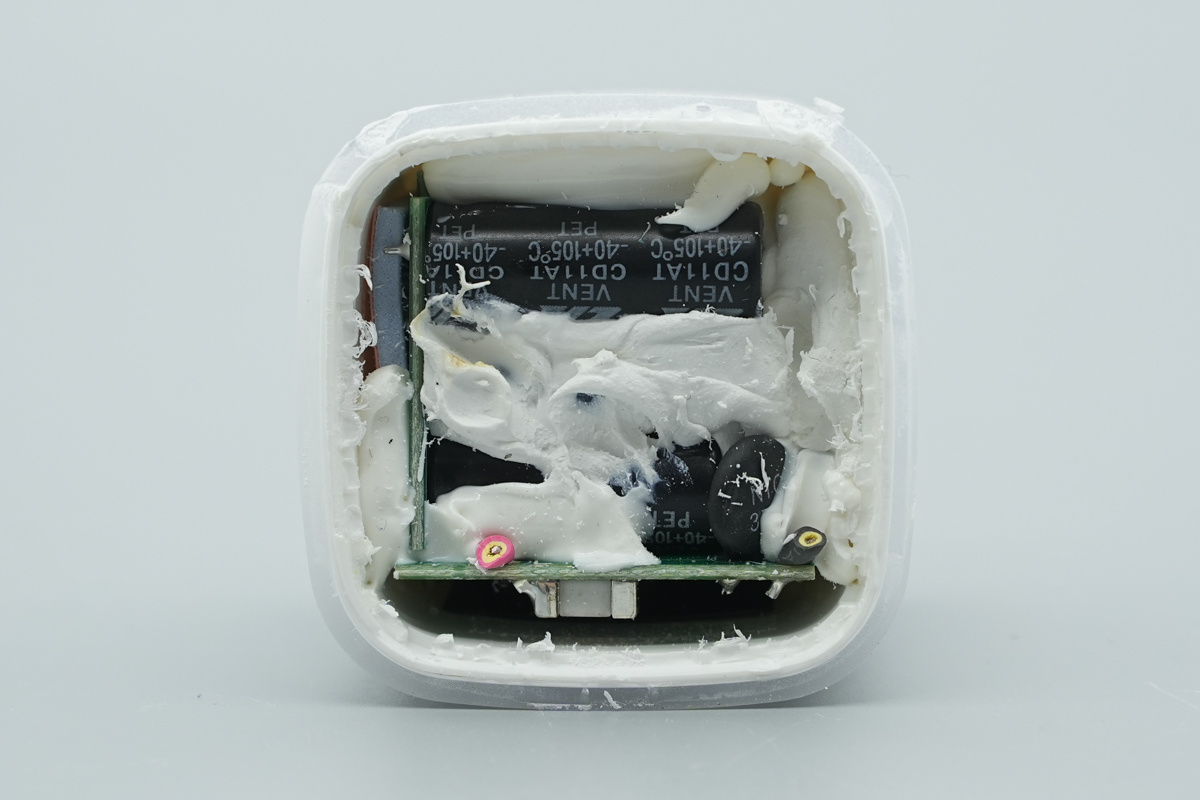
The PCBA’s high-voltage electrolytic caps and other key components are covered in white thermal potting compound.
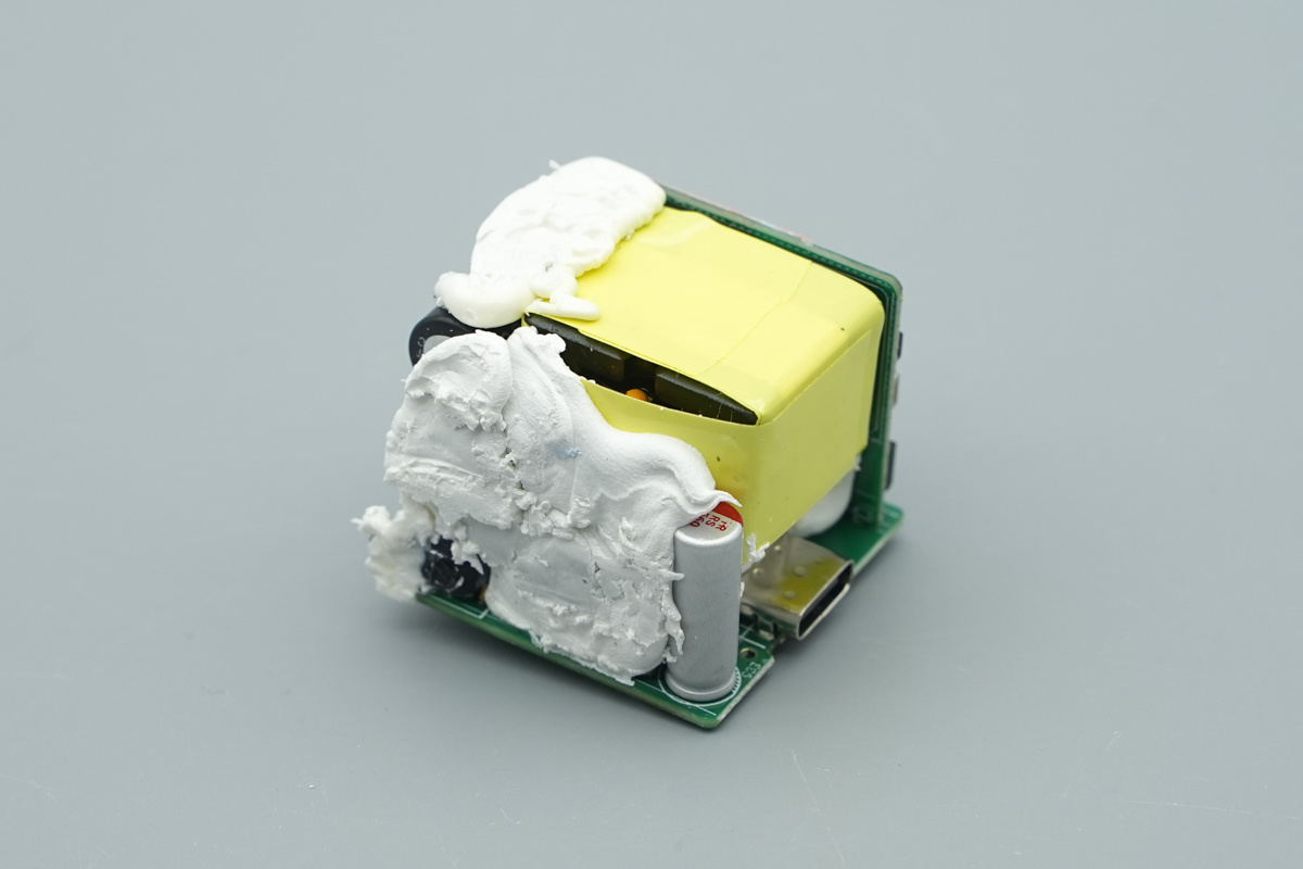
The PCBA module utilizes a two-PCB layout. Gaps are filled with white thermal potting compound to increase structural stability and drop resistance.
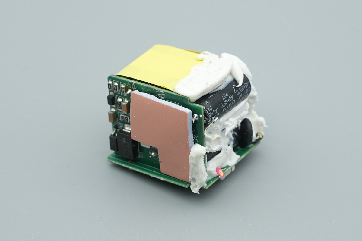
The other side of the PCBA features a pink thermal pad designed to conduct heat from the primary master control chip to the outer casing.
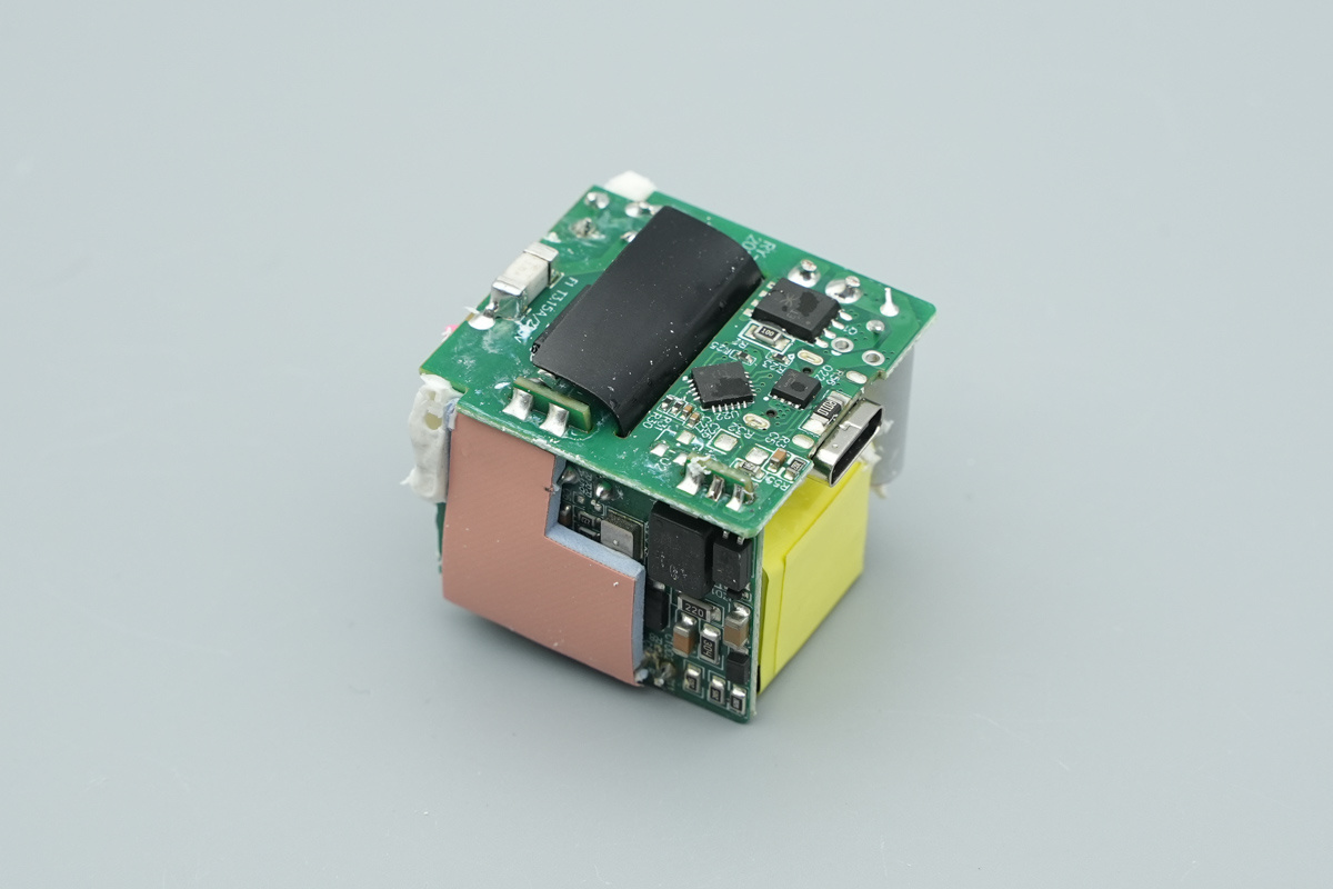
A Mylar sheet is installed between the primary and secondary circuits on the back of the PCBA
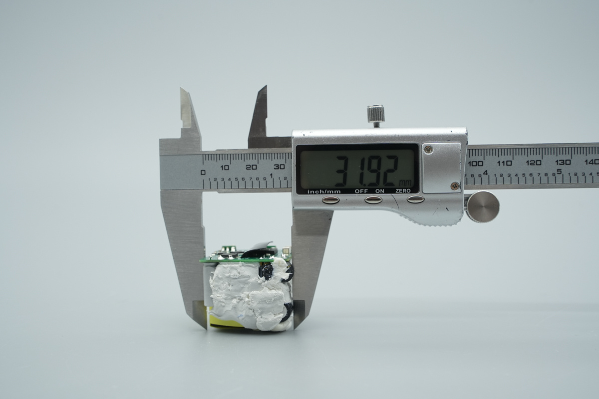
The length of the PCBA is about 31.92mm (1.257 inches).
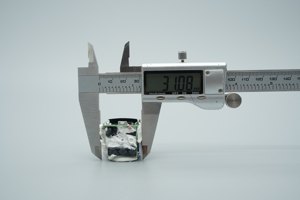
The width of the PCBA is about 31.08mm (1.224 inches).
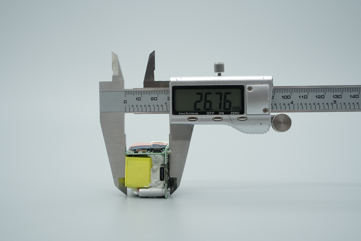
The thickness of the PCBA is about 26.76mm (1.054 inches).
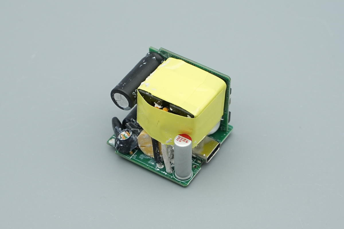
Once the white thermal potting compound is removed, the PCBA’s layout is exposed, showing the transformer along with the high-voltage and low-voltage filter caps.
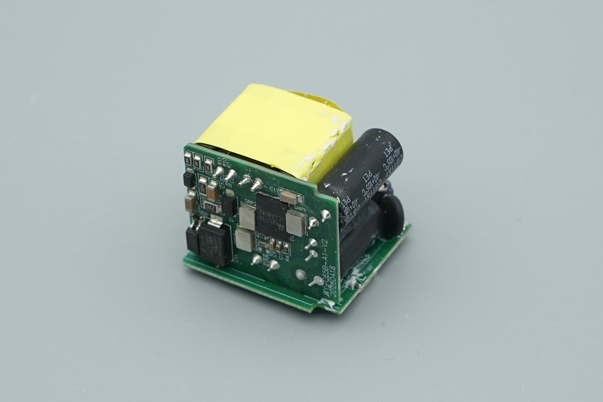
The other side of the PCBA features the integrated GaN power IC and the SMD Y-cap.
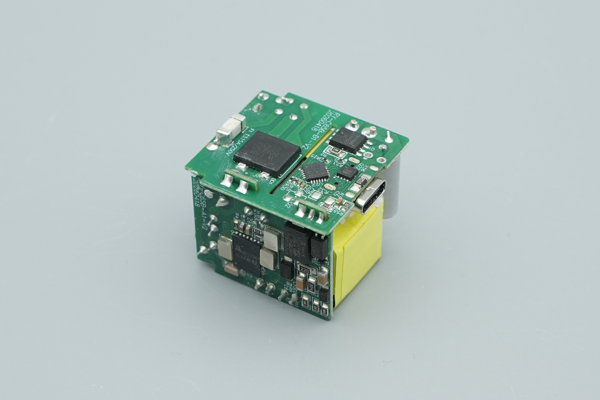
The PCBA’s backside features a clear defind between the primary and secondary circuits, with a wide isolation gap.
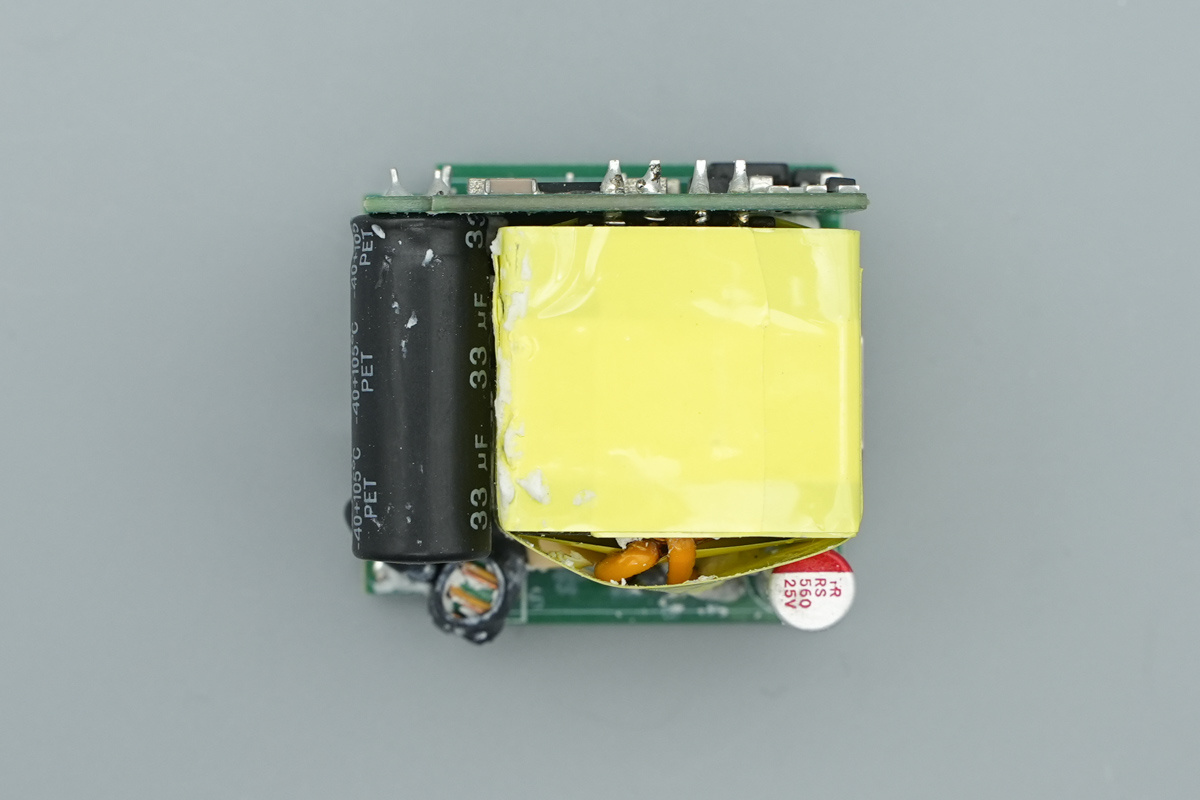
Looking at the PCBA from above, the high-frequency transformer takes up nearly 50% of the mainboard's real estate, next to the high-voltage filter cap.
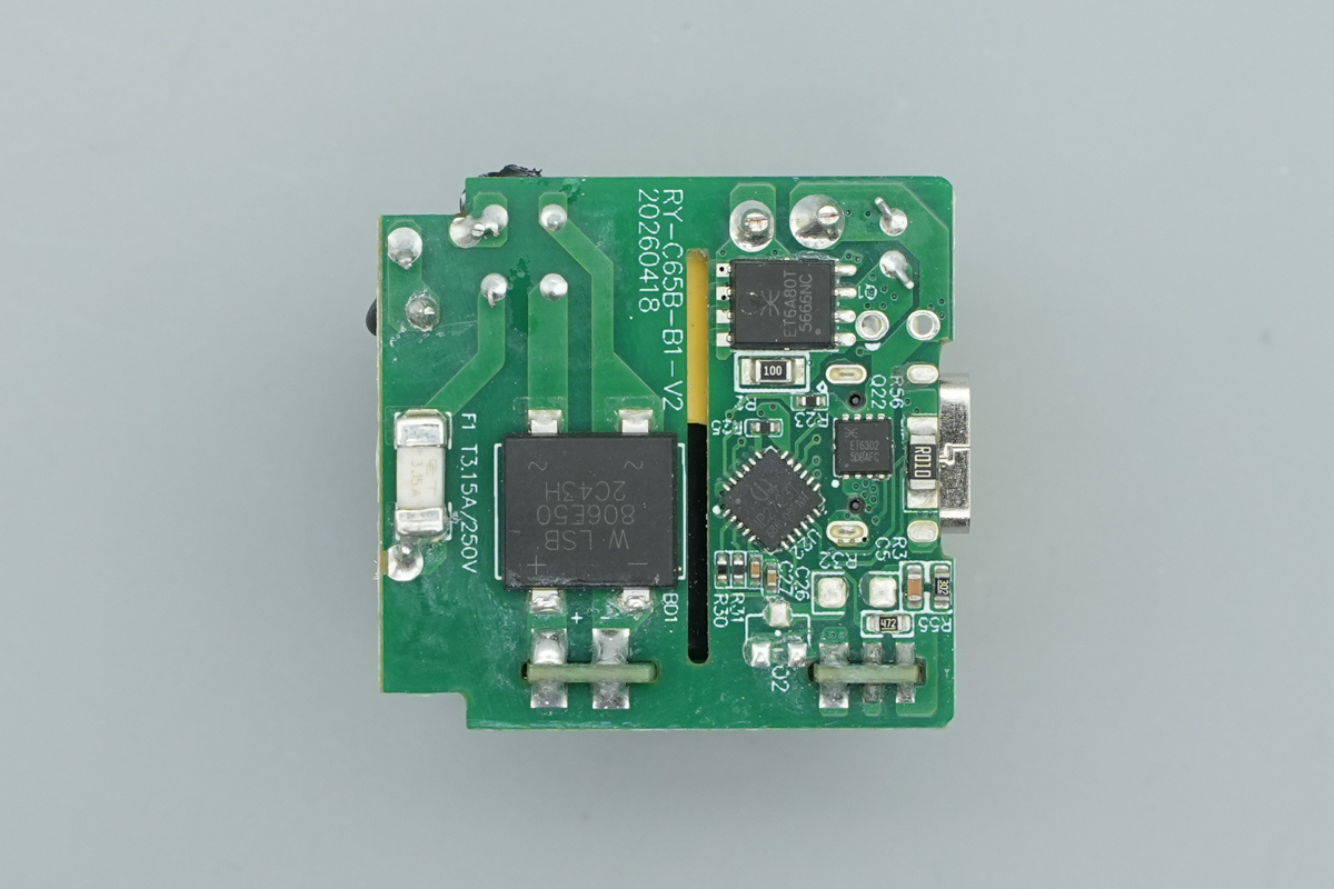
This is the back side of the PCBA, primary high-voltage side on the left, secondary low-voltage side on the right.
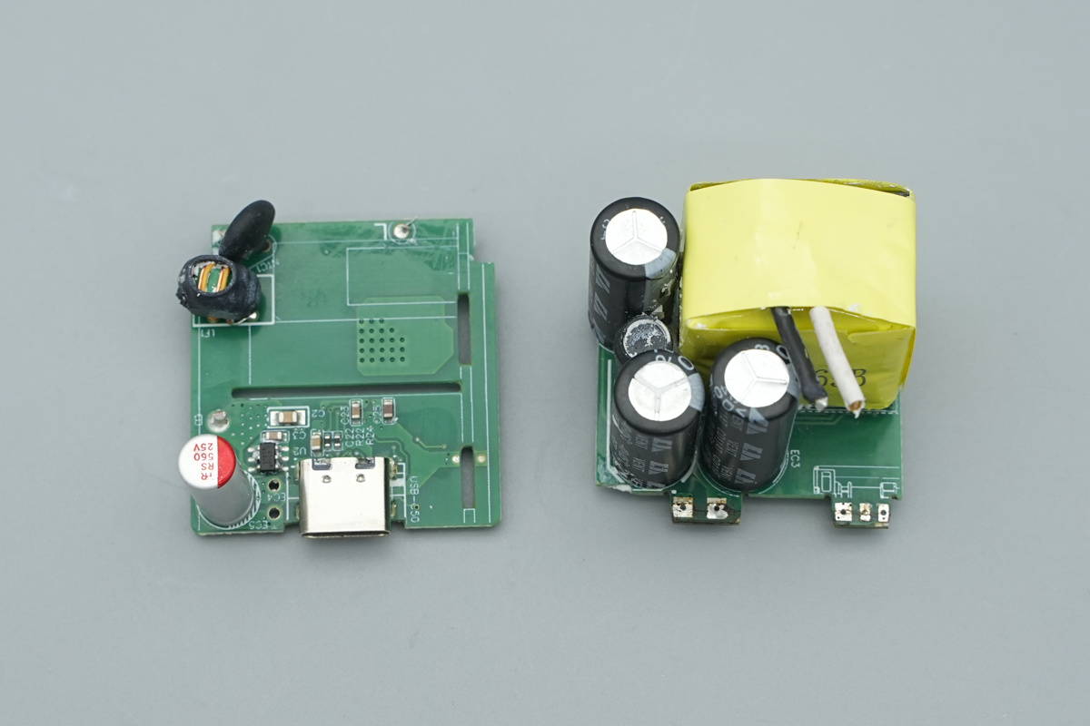
Next, separating the two PCBs.
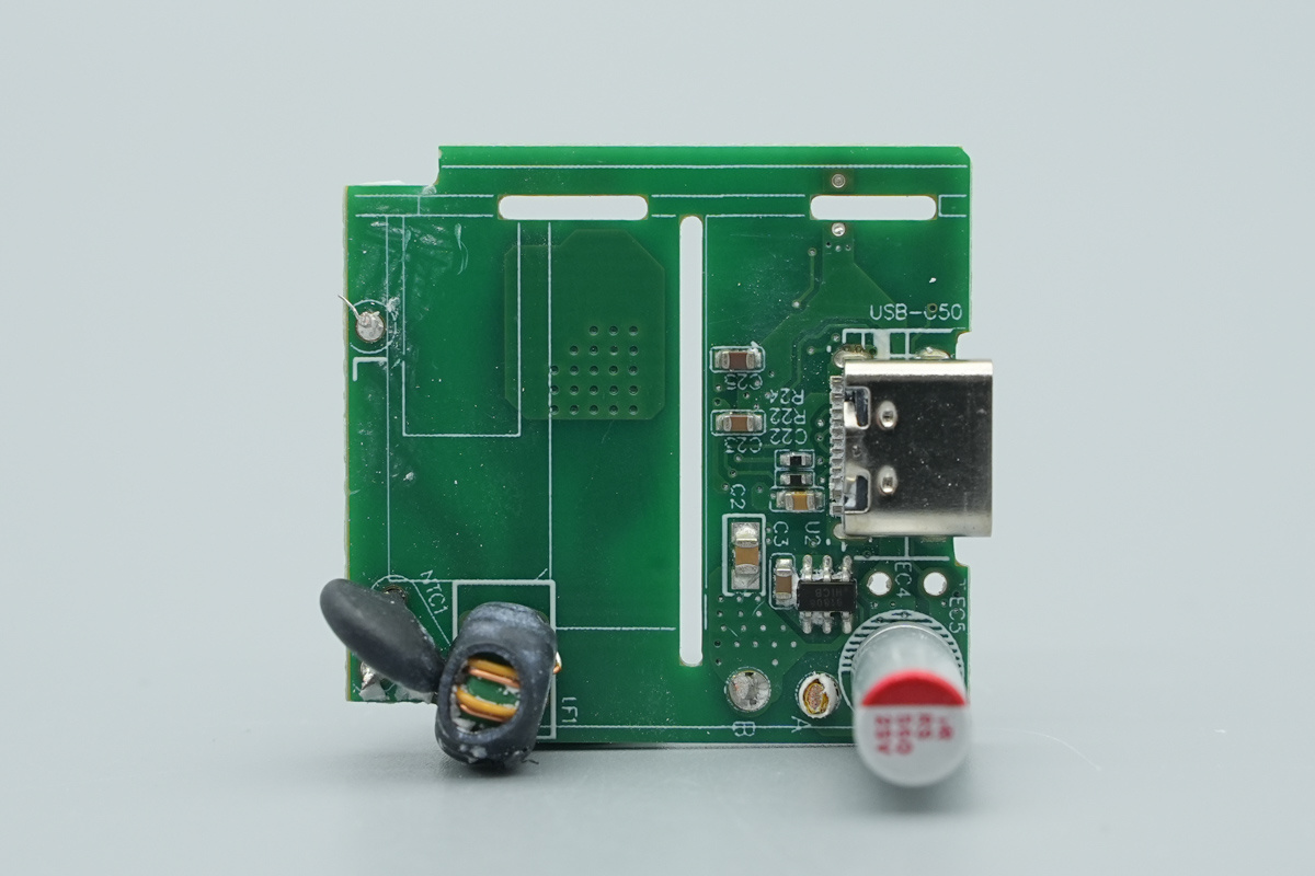
The base PCB features the USB-C receptacle, solid cap, and the common-mode choke.
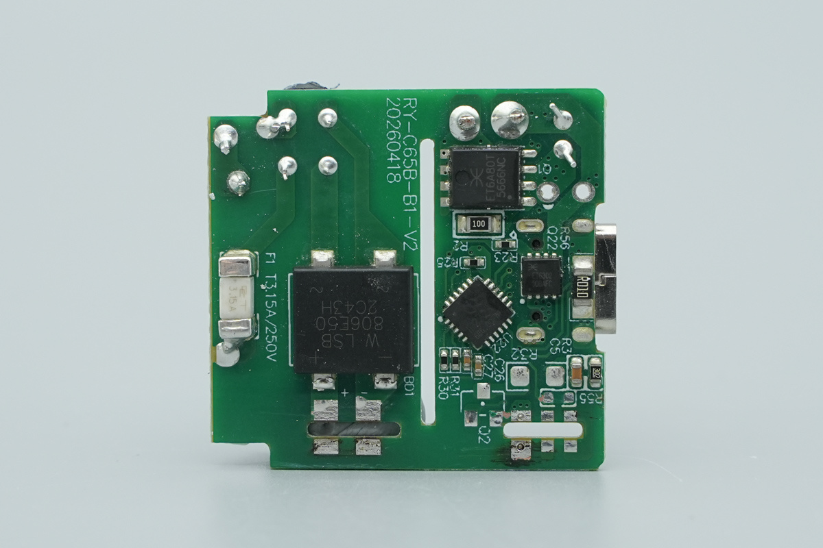
The back side of the PCB hosts the rectifier bridge , the synchronous rectifier MOSFET, the protocol chip, and the VBUS MOSFET.
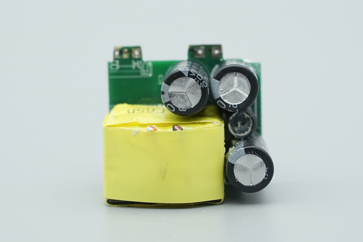
The front of the side PCB features the high-voltage filter cap, the transformer, and the I-shaped choke.
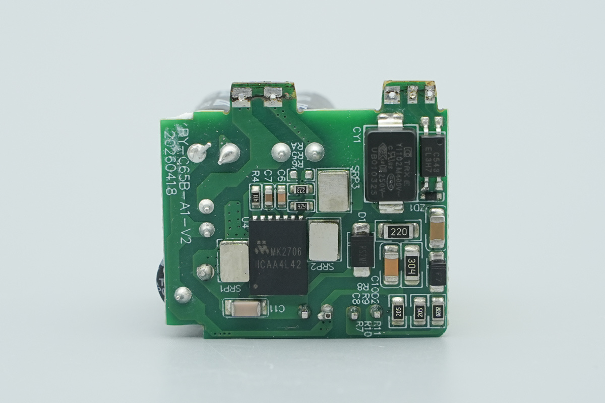
The back of the PCB features the integrated GaN power IC, the SMD Y-cap, and the optocoupler.
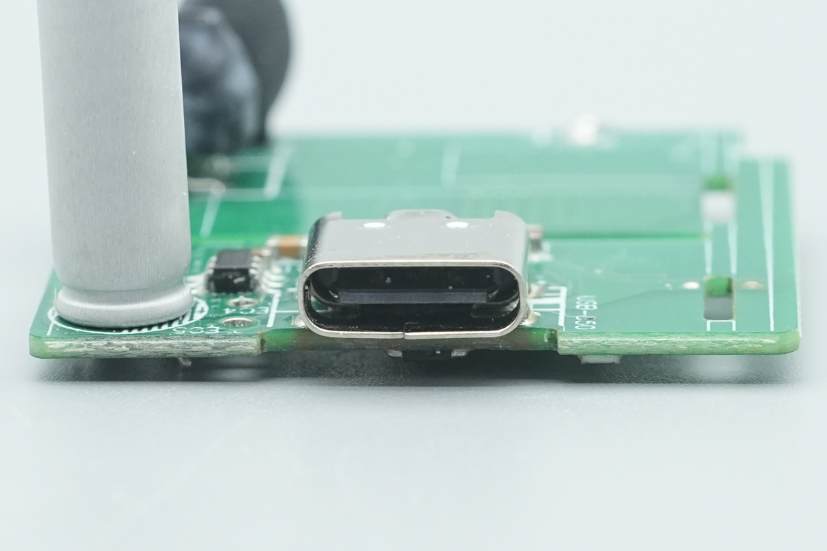
The USB-C receptacle utilizes a black plastic sheet design.
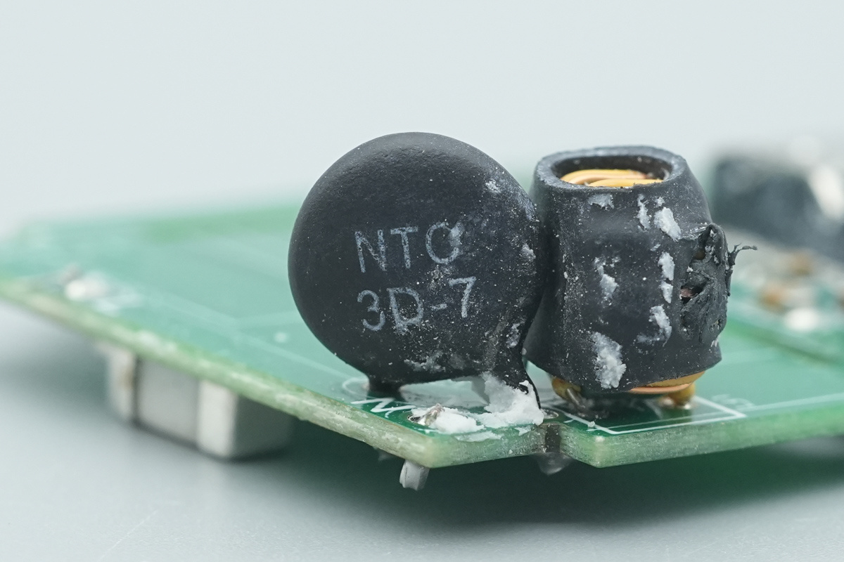
This is the NTC thermistor at the input end, marked NTC 3D-7. It serves to suppress inrush current during startup.
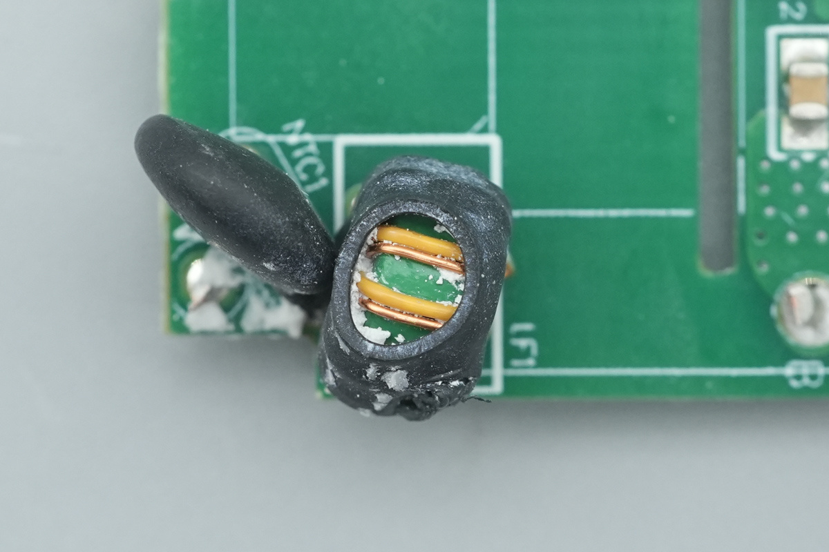
The common-mode choke uses a bifilar winding design to effectively filter out EMI.
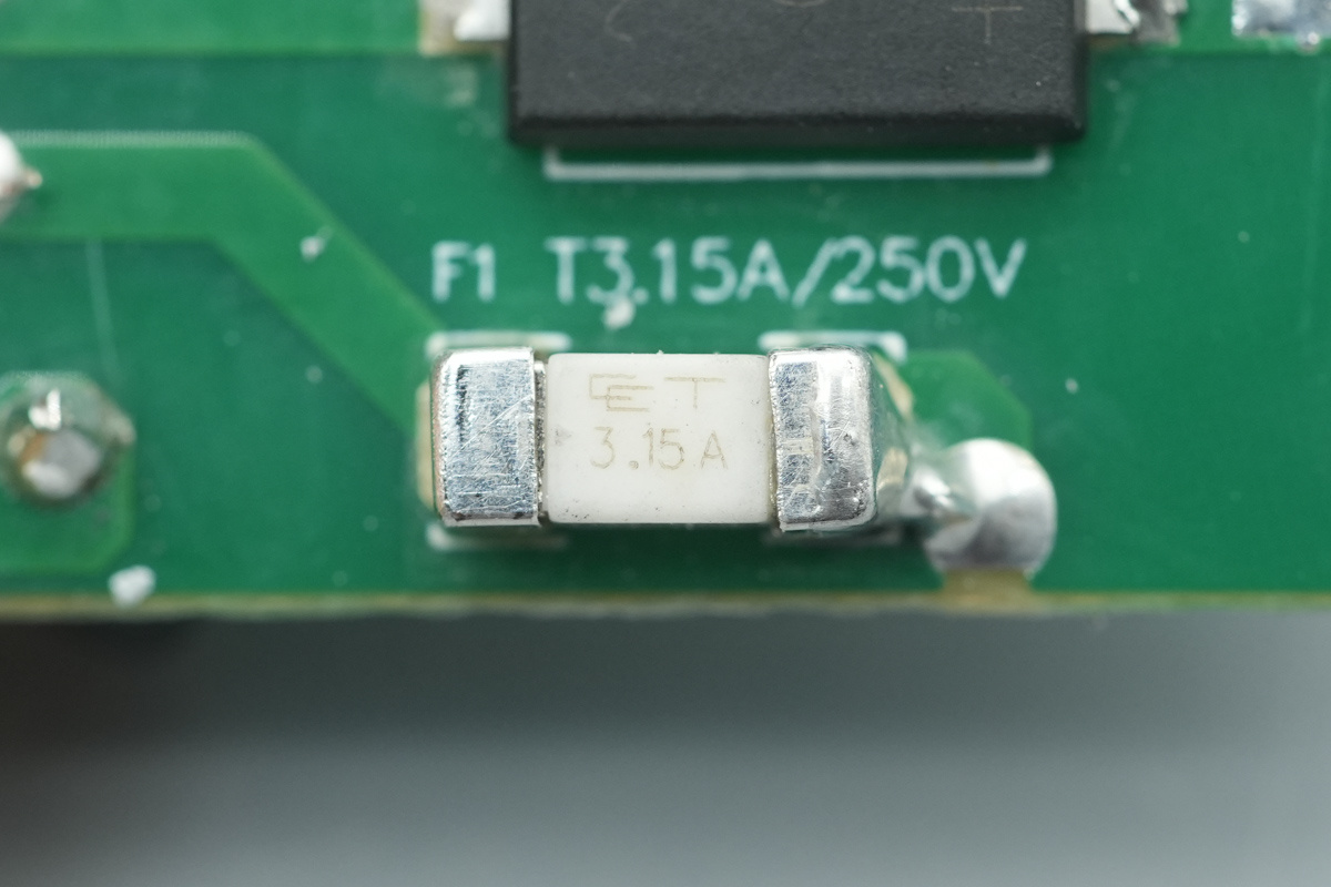
This is the SMD fuse located at the input end.
An I-shaped choke located between the two caps.
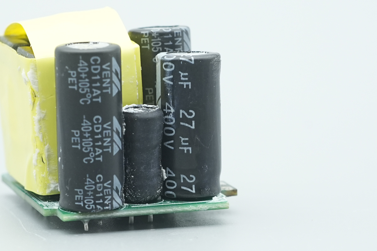
The three high-voltage filter caps are from CH. Two of them are 400V 33μF, the third one is 400V 22μF.
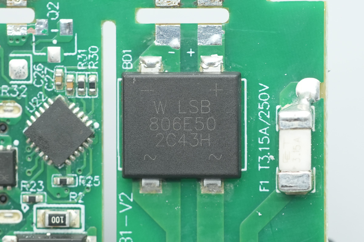
The rectifier bridge from World, model LSB806E50, 600V 8A, in an LSB package.
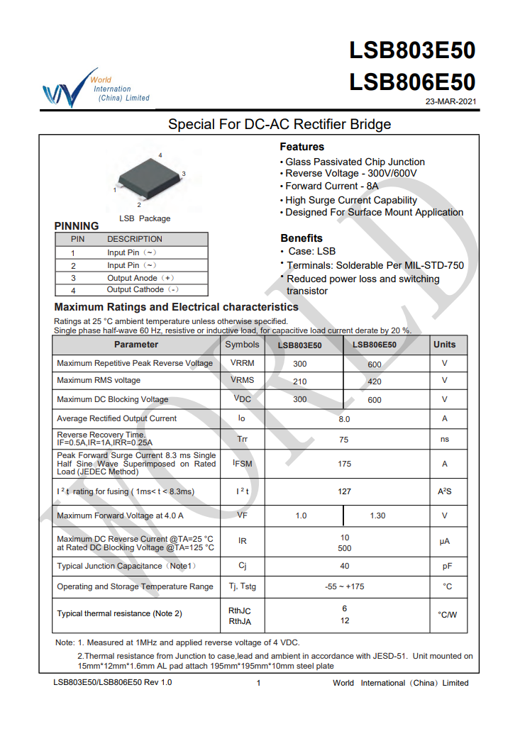
Here is the info about World LSB806E50.
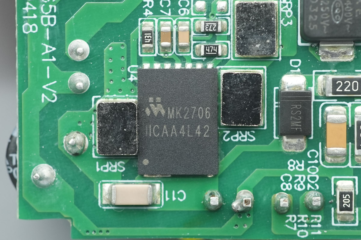
The integrated GaN power IC is from MERAKI, model MK2706IDG. It is a QR controller specifically optimized for PD fast-charging applications, featuring an integrated 700V/170mΩ GaN FET and housed in a DFN6x8 package.
It supports an ultra-wide VCC operating voltage range of 9V to 85V, enabling broad-range PD/PPS outputs from 3.3V to 21V without the need for additional auxiliary VCC windings or external linear regulators.
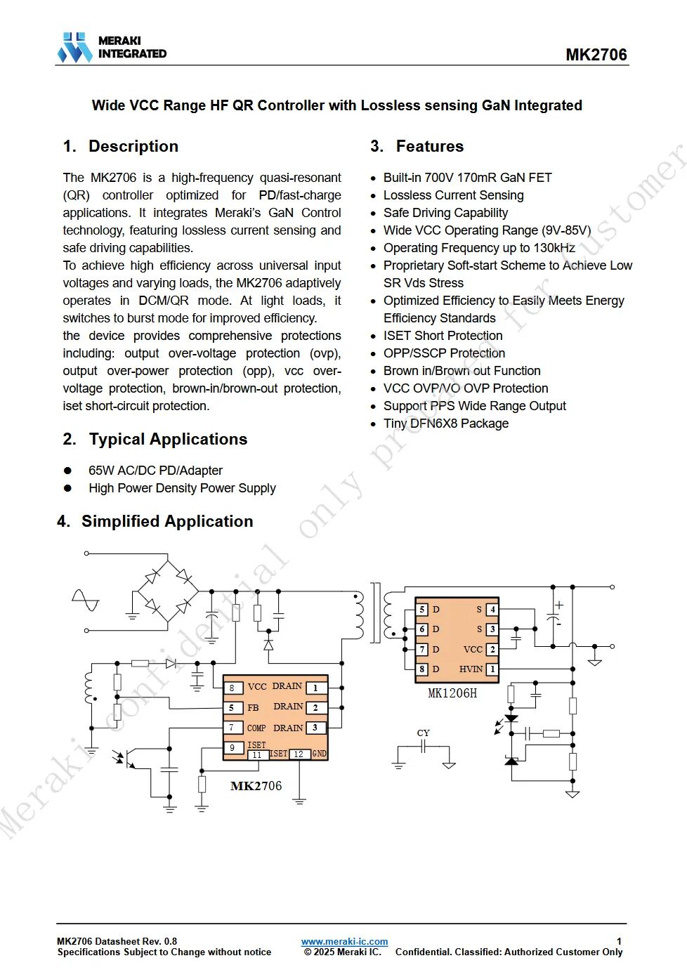
It can operate in either DCM or QR mode, and it automatically switches to burst mode under light-load conditions to optimize conversion efficiency across the entire load range, effortlessly meeting various energy efficiency standards.
Beyond efficiency, this chip packs a suite of robust protections into its compact DFN6x8 package—ranging from OVP and OPP to VCC protection and secondary short-circuit safeguards—guaranteeing stable and reliable performance.
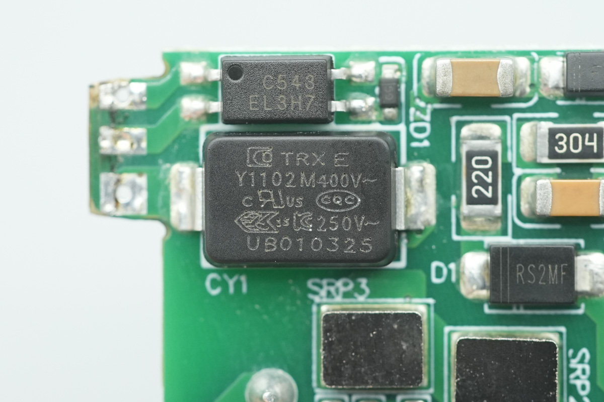
The SMD Y-cap is from TRX. Compact and lightweight, designed specifically for high-density power modules like GaN chargers.
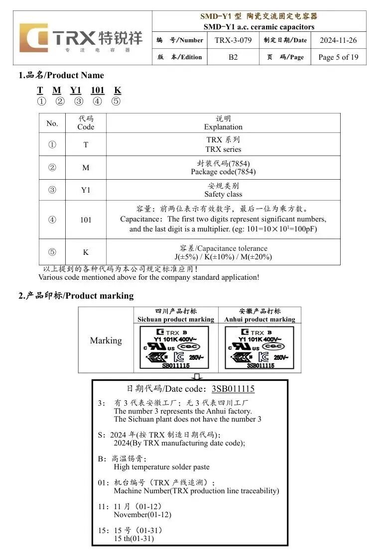
Here is the info about TRX SMD Y-cap.
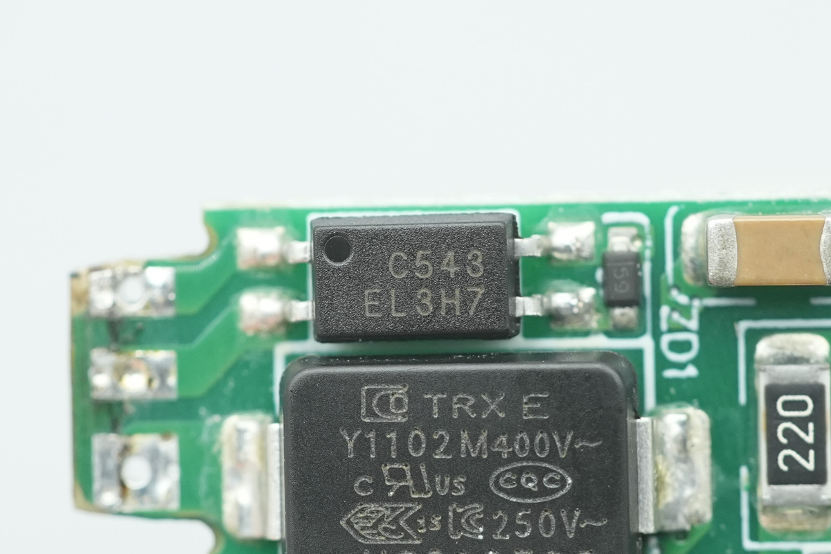
The optocoupler is supplied by Everlight, model EL3H7.
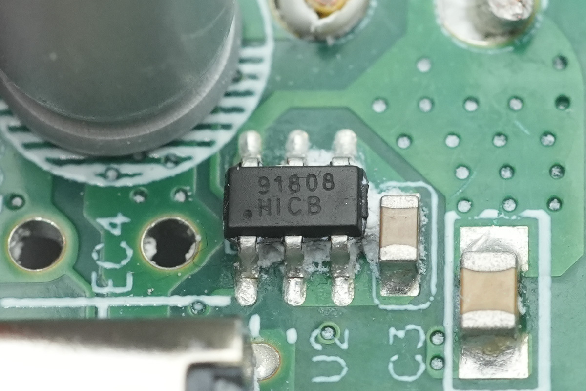
The synchronous rectifier chip is from MERAKI, model MK91808H. It is a compact SR controller designed for flyback topologies, which offers broad support for CCM, DCM, and QR modes and leverages proprietary self-powered technology to enable high-side application, eliminating the complexity of an additional auxiliary winding.
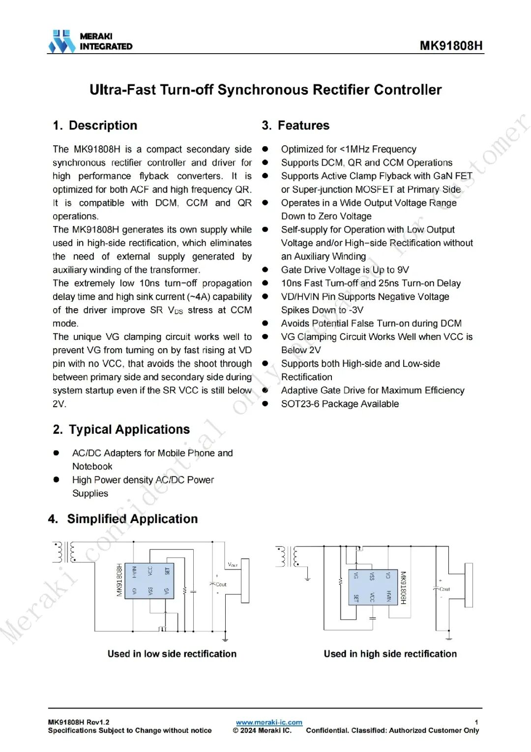
Furthermore, with a 10ns turn-off delay and 4A of sink current, the MK91808H is engineered for reliable performance even in CCM mode.
Its proprietary switching logic maximizes MOSFET conduction time for superior efficiency, while intelligent DCM ringing detection prevents false turn-ons. To ensure further safety, the integrated GATE clamp protects the MOSFET from premature triggering before and during the startup phase.
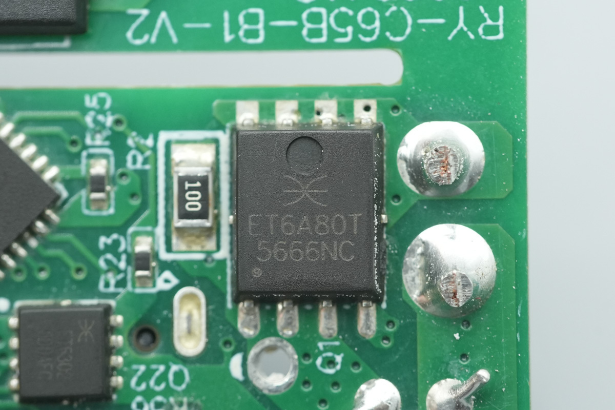
The synchronous rectifier MOSFET is from Eternal, model ET6A80T, NMOS, 100V and 3.7mΩ, housed in a PDFN5x6 package.
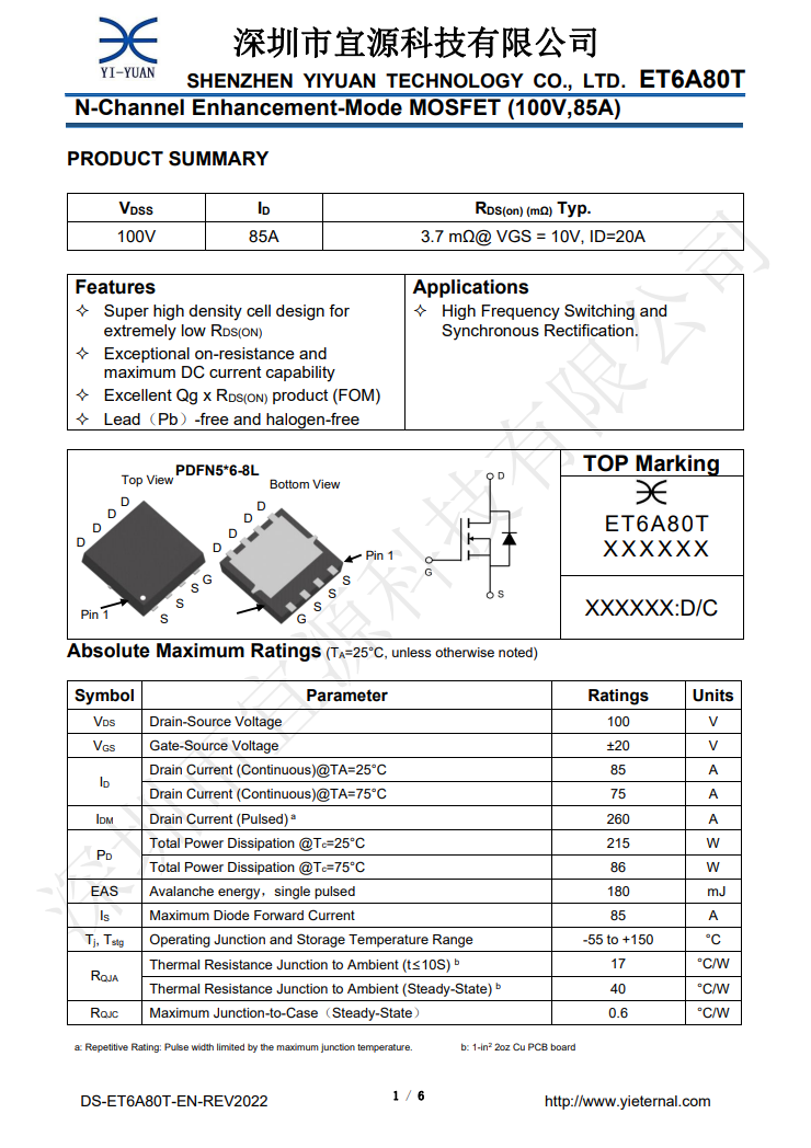
Here is the info about Eternal ET6A80T.
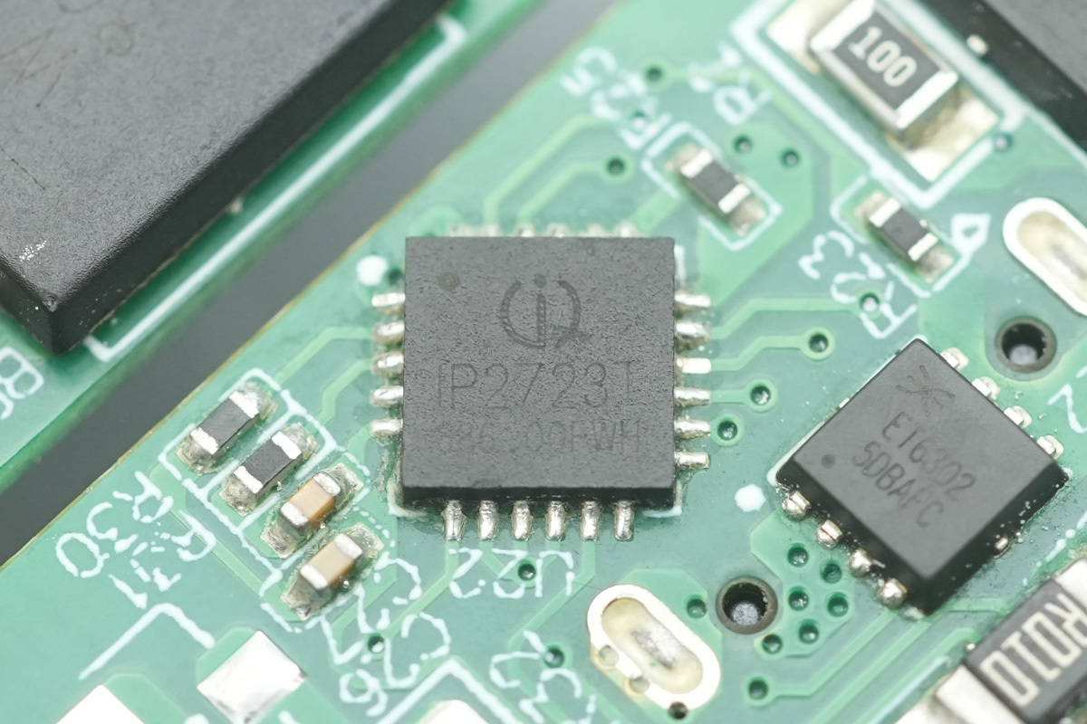
The protocol chip is from INJOINIC, model IP2723T, housed in a QFN24 package. It has achieved USB-IF PD3.0 PPS certification (TID: 3135) and is a highly integrated fast-charging protocol IC designed for USB output ports.
The IP2723T supports a wide array of fast-charging protocols, including USB Type-C DFP, PD2.0/3.0, PPS, HVDCP QC4/QC4+, QC3.0/2.0, FCP, SCP, AFC, MTK PE+ 2.0/1.1, Apple 2.4A, BC1.2, and Samsung 2.0A.
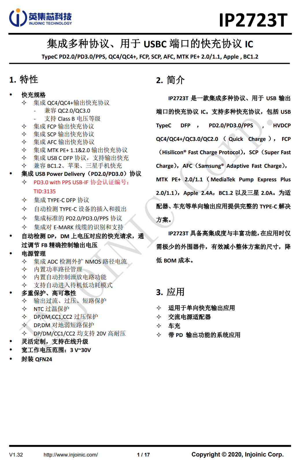
The IP2723T provides a complete USB Type-C solution for unidirectional output applications such as power adapters and car chargers. Furthermore, thanks to its high integration and rich feature set, it requires minimal peripheral components, which effectively reduces the overall footprint and lowers the BOM.
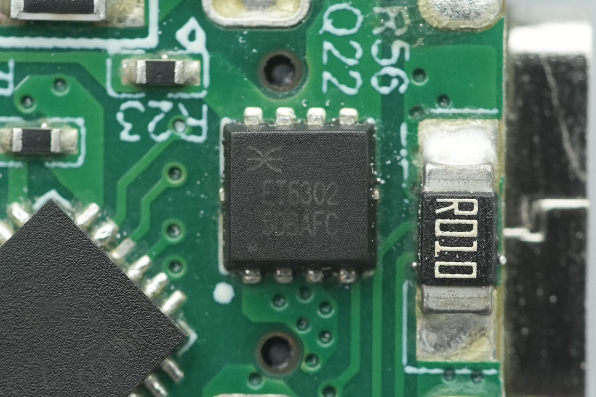
The VBUS MOSFET is from Eternal, model ET6302, NMOS, 30V and 5mΩ, housed in a PDFN3333 package.
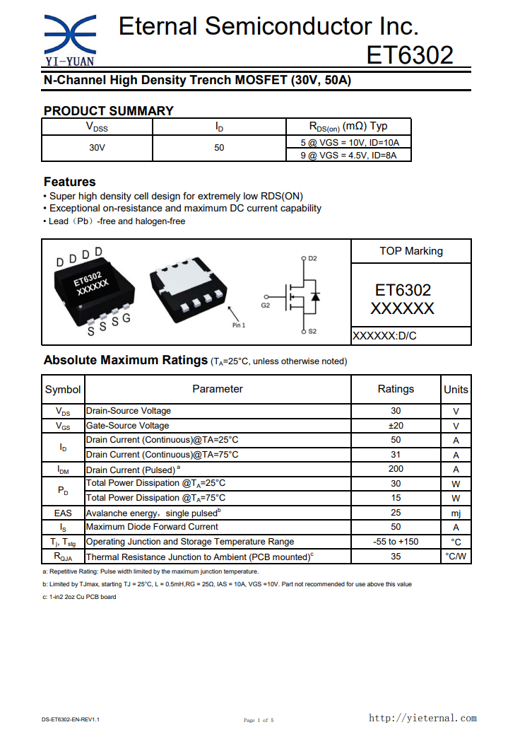
Here is the info about Eternal ET6302.
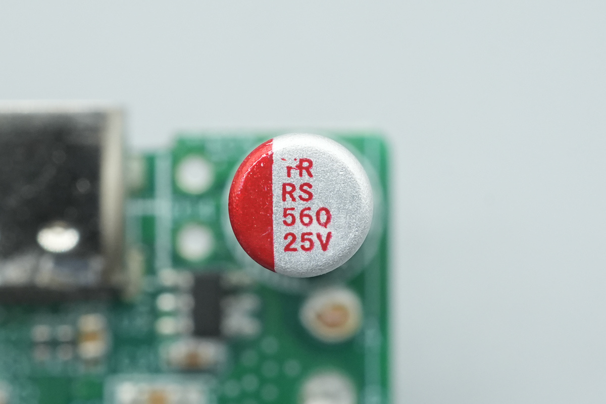
A low-voltage solid cap at output filter end, 25V/560μF.
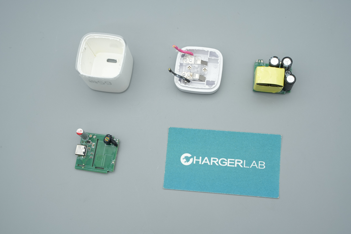
Well, those are all components of the Ruiyuan 65W GaN PD Fast Charger.
Summary of ChargerLAB
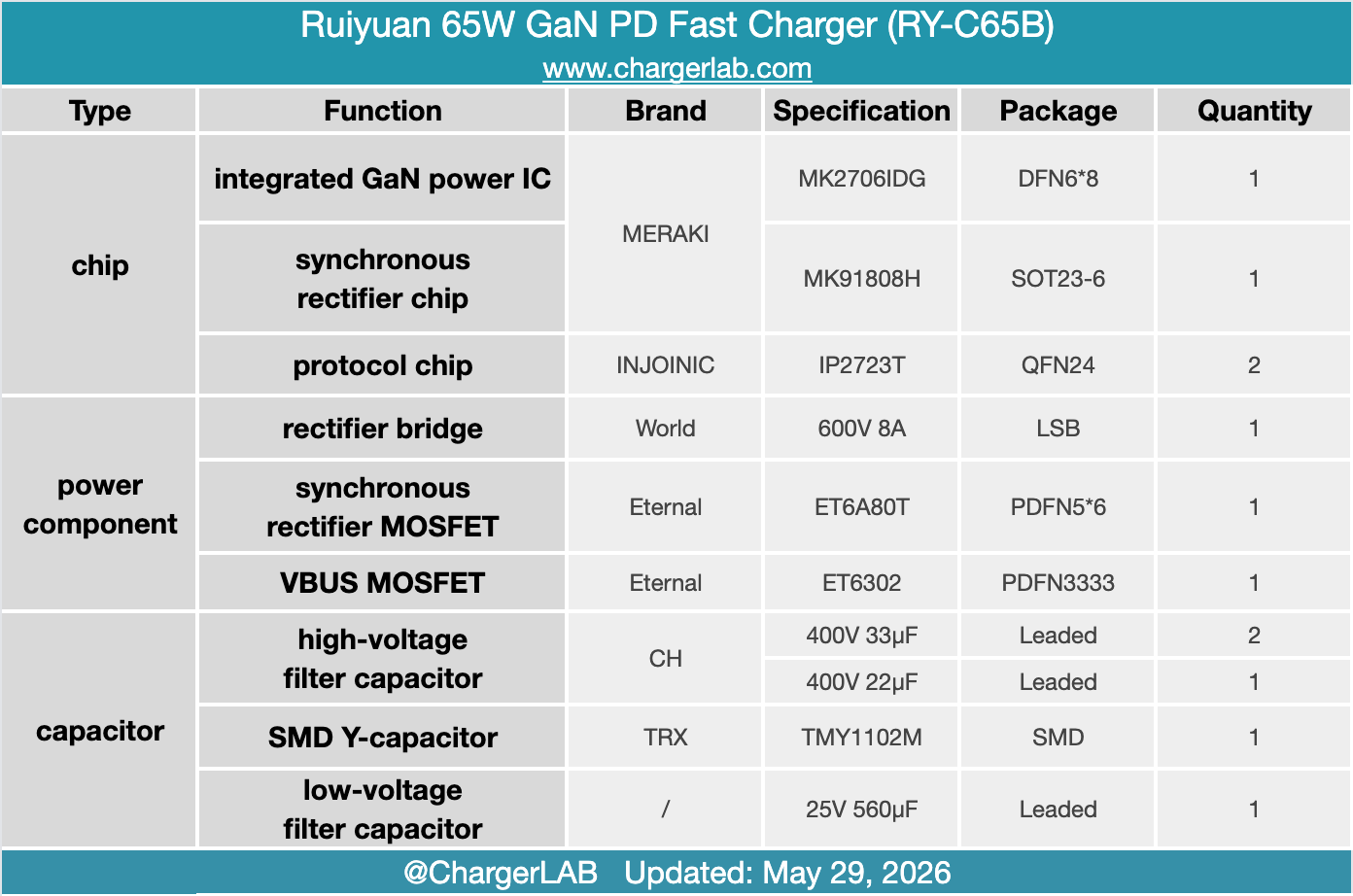
Sporting a clean, minimalist aesthetic with foldable prongs, the Ruiyuan 65W GaN charger is built for travel. It is highly versatile, supporting a comprehensive range of protocols like QC, PD, and PPS—delivering enough power (65W) to drive anything from smartphones to ultrabooks.
Our deep dive into the internals shows a robust construction. To combat the heat generated by such a compact high-power design, the PCBA is reinforced with abundant white thermal potting compound and backed by a thermal silicone pad.
Performance-wise, the charger relies on an integrated GaN power IC and synchronous rectifier chip from MERAKI, matched with an INJOINIC protocol chip. This streamlined, high-efficiency architecture makes it a standout product that refuses to compromise on either form factor or power.
Related Articles:
1. 140W Fast Charging Unleashed: STMicroelectronics’ PowerGaN Reference Design
2. V.2.0.3 | The New Software Version of ChargerLAB POWER-Z KM003C
3. Teardown of Baseus EnerFill FH22 100W GaN PD Fast Charger