Introduction
OPPO unveils its new SUPERVOOC 120W Super Flash Charge Power Bank 15000 in response to the latest 3C Chinese standard for mobile power safety. Representing the industry’s first wave of products to feature intelligent safety monitoring, this device highlights OPPO’s role as a core contributor to the new technical specs.
The power bank’s robust safety management system has also gained national attention, earning high praise from CCTV-12’s “Public Safety Open Class” for its commitment to user security and reliable performance.
OPPO’s SUPERVOOC 120W Super Flash Charge Power Bank packs a massive 15,000mAh capacity and a 120W output, making it an ideal fast-charging companion for both OPPO handsets and a wide array of PD-compatible electronics.
The true game-changer is the visual battery health interface, which fully satisfies the latest national standards for intelligent monitoring. By simply plugging the power bank into a computer, users can instantly pull up critical diagnostics including charge cycles, battery health metrics, voltage, and temperature, ensuring total control and security for daily use.
Let's dive into our full teardown to explore its internal build and the components powering this device.
Product Appearance
The packaging box displays a rendering of the device on the front, with the product name "OPPO SUPERVOOC 120W Super Flash Charge Power Bank 15000" printed clearly at the top for a minimalist look.
The back of the box lists five main features:premium OPPO safety cells, a 120W / 15,000mAh capacity upgrade, compatibility with 100W protocols, a new interstellar-inspired design, and 3C certification which ensures flight safety and supports software-based status diagnostics.
The side of the box includes an official OPPO anti-counterfeiting label, which provides a scannable QR code under the scratch-off layer for quick authenticity verification.
The box contains the power bank, a compatible charging cable, and the user manual.
A white USB-A to USB-C charging cable is provided in the box.
The length of the cable is approximately 30cm.
It features a dual-tone design in beige and bright orange, with a skin-friendly matte finish on the front face, elegantly accented by the OPPO brand logo.
Located on the top orange area are four hidden LED battery indicators, featuring a design with rounded, chamfered edges.
Pressing the power button wakes the device and lights up the indicators with a soft white glow, providing quick and clear battery level visibility.
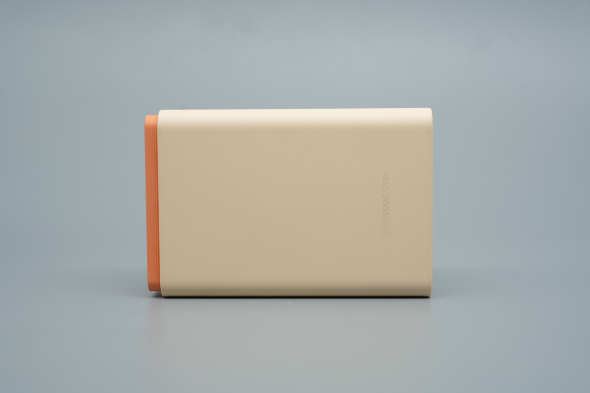
The side of it maintains a minimalist look, with a vertical "SUPERVOOC 120W" print on the right side indicating its support for OPPO’s high-power flash charging.
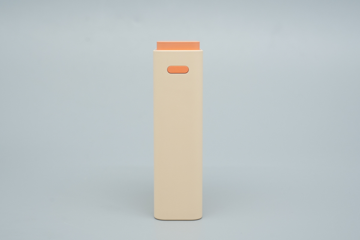
The side edge features a pill-shaped power button, styled in an orange hue that complements the top cover.

The edge of the top orange area features a striped texture design, adding an extra touch of refinement to the product.
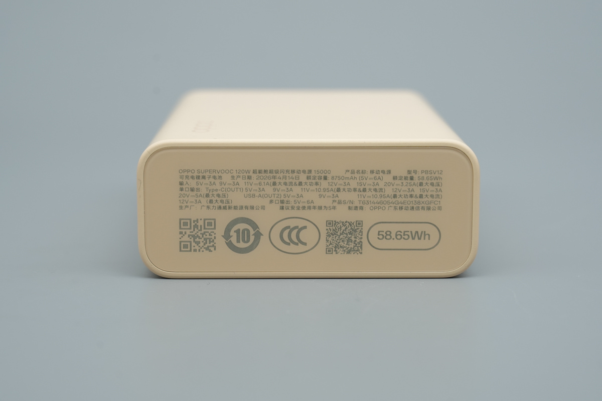
The base of it carries the product nameplate with technical specs, matching the info displayed on the outer packaging.
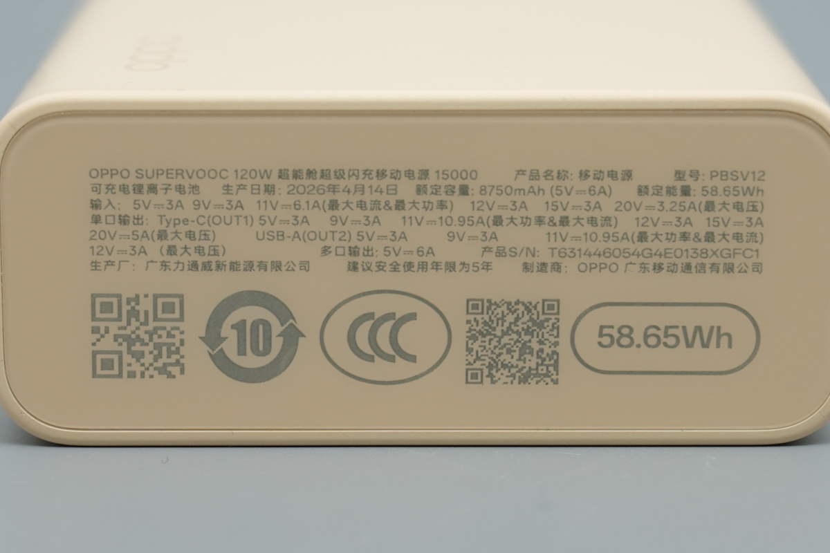
Technical spes:
The OPPO SUPERVOOC 120W Super Flash Charge Power Bank 15000
Product Name: Power Bank
Model: PBSV12
Manufacturing Date: April 14, 2026
Rated Capacity: 8,750mAh (5V 6A)
Rated Energy: 58.65Wh
Input: 5V/3A, 9V/3A, 11V/6.1A (Max), 12V/3A, 15V/3A, 20V/3.25A (Max)
Single-Port Output:
Type-C (OUT1): 5V/3A, 9V/3A, 11V/10.95A (Max), 12V/3A, 15V/3A, 20V/5A (Max)
USB-A (OUT2): 5V/3A, 9V/3A, 11V/10.95A (Max), 12V/3A (Max)
Multi-Port Output: 5V/6A
Certification: This product is Chinese 3C certified.
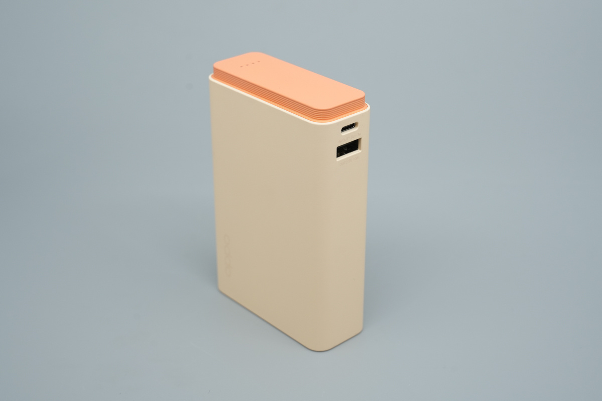
The side of the top orange area houses the input/output interface panel, which includes one bidirectional USB-C fast-charging port and one USB-A output port.
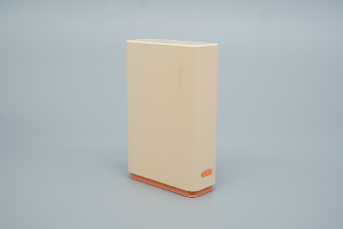
The power bank displays a striking, highly recognizable color-blocked design when placed in an upright position.
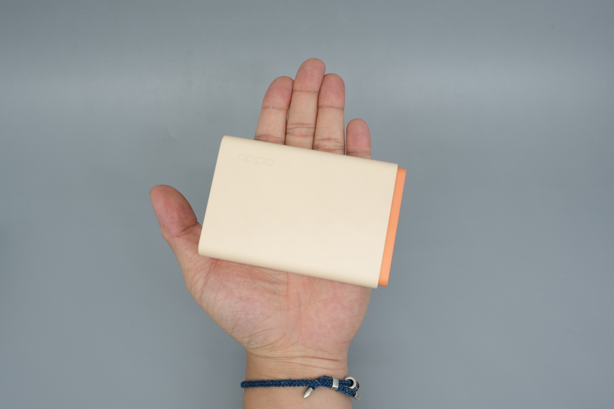
That's how big it is in the hand.
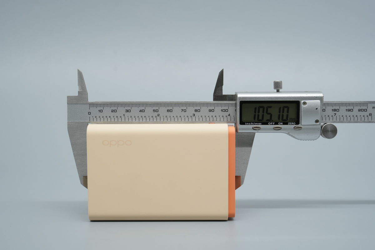
The length of the power bank is about 105.10mm (4.138 inches).
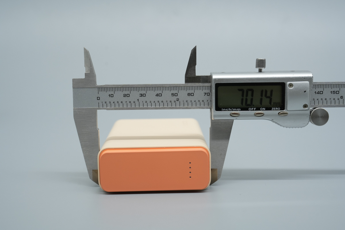
The width of the power bank is about 70.14mm (2.761 inches).
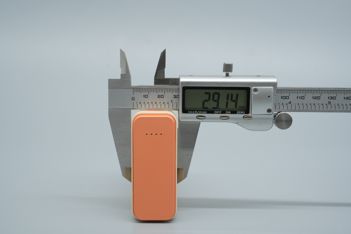
The thickness of the power bank is about 29.14mm (1.147 inches).
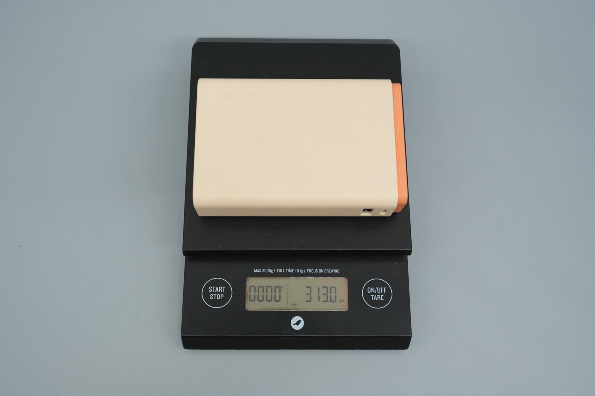
The weight is about 313.0g (11.04 oz).
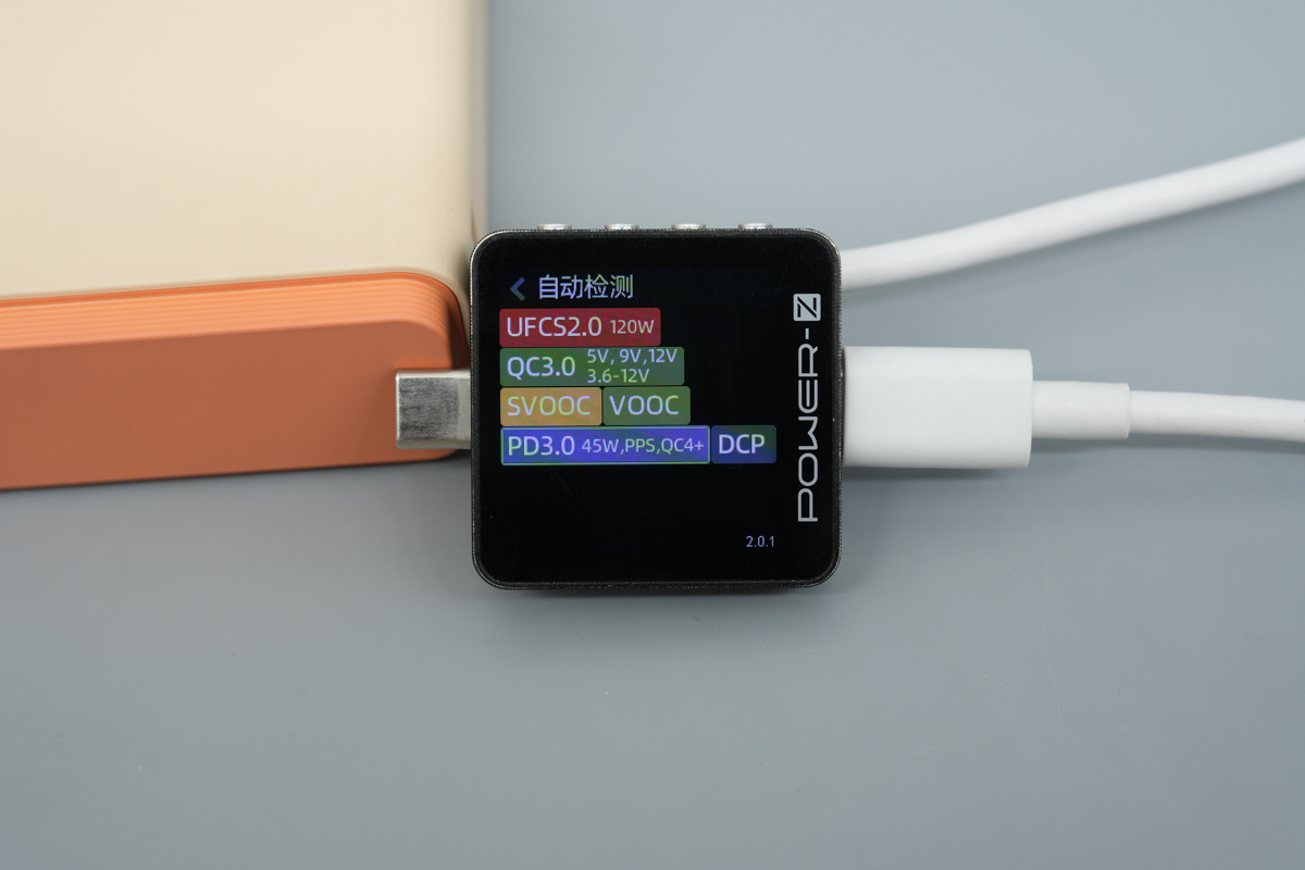
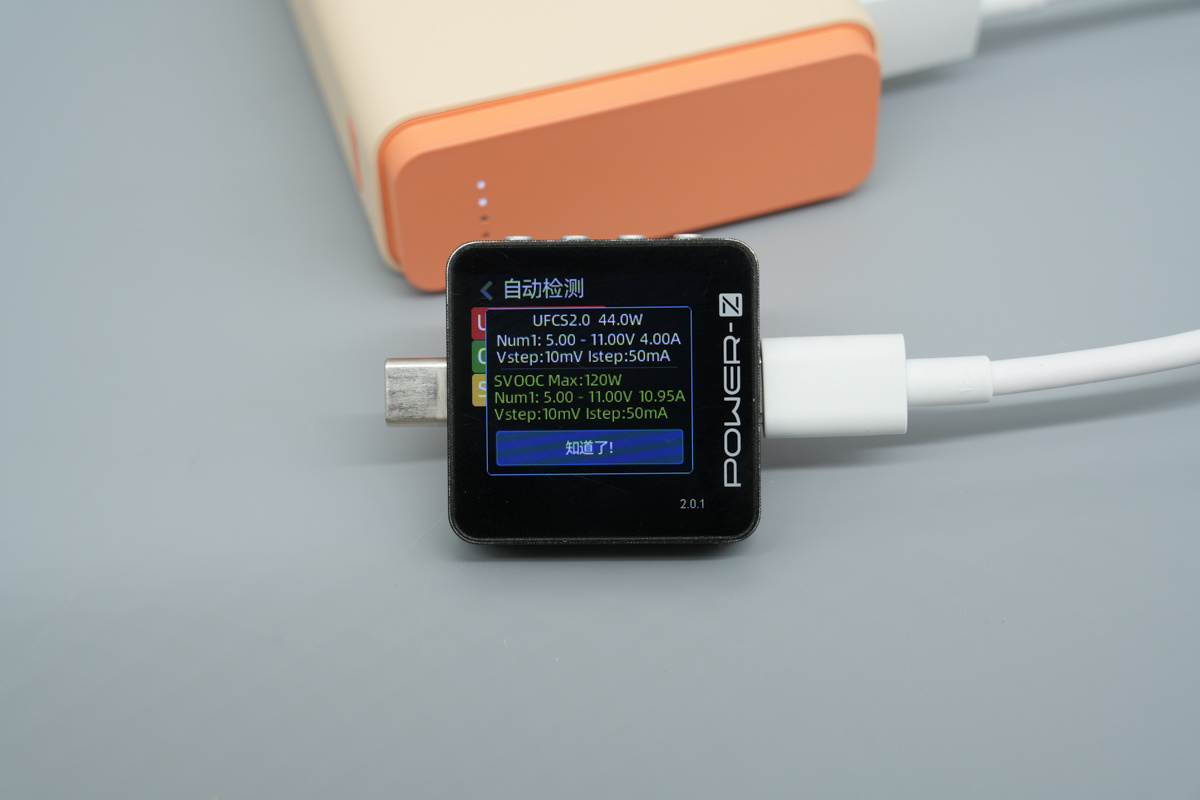
ChargerLAB POWER-Z KM003C shows that the USB-C port supports UFCS2.0, QC3.0, SVOOC, VOOC, PD3.0\PPS and DCP.
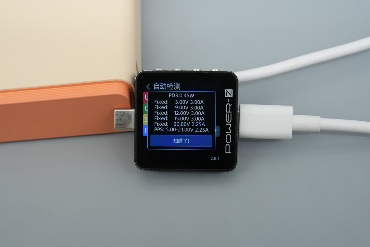
And it also supports four fixed PDOs of 5V3A, 9V3A, 12V3A, 15V3A and 20V2.25A, and features PPS subset: 5-21V 2.25A.
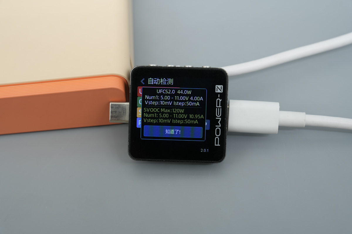
And the USB-C port also supports the UFCS of 5-11V 4A, and features SVOOC subset: 5-11V 10.95A.
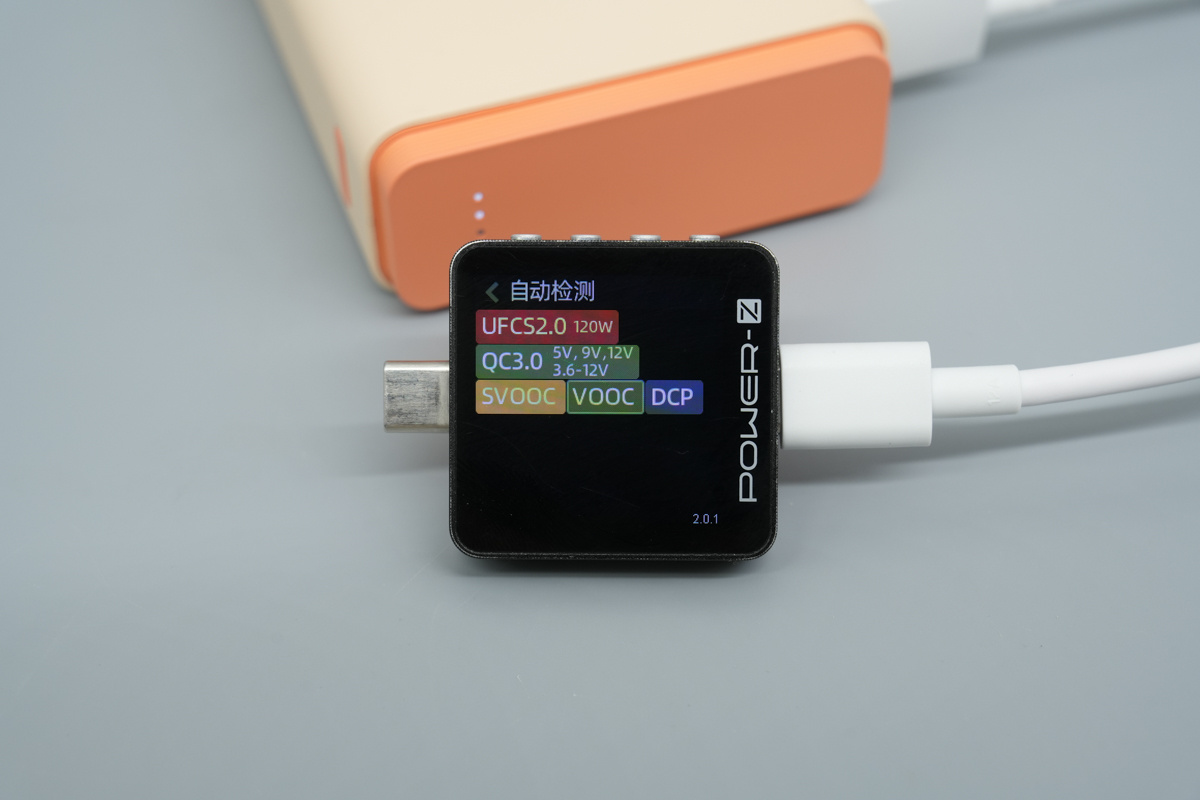
ChargerLAB POWER-Z KM003C shows that the USB-A port supports UFCS, QC3.0, SVOOC, VOOC and DCP.
And the USB-A port also supports the UFCS of 5-11V 4A, and features SVOOC subset: 5-11V 10.95A.
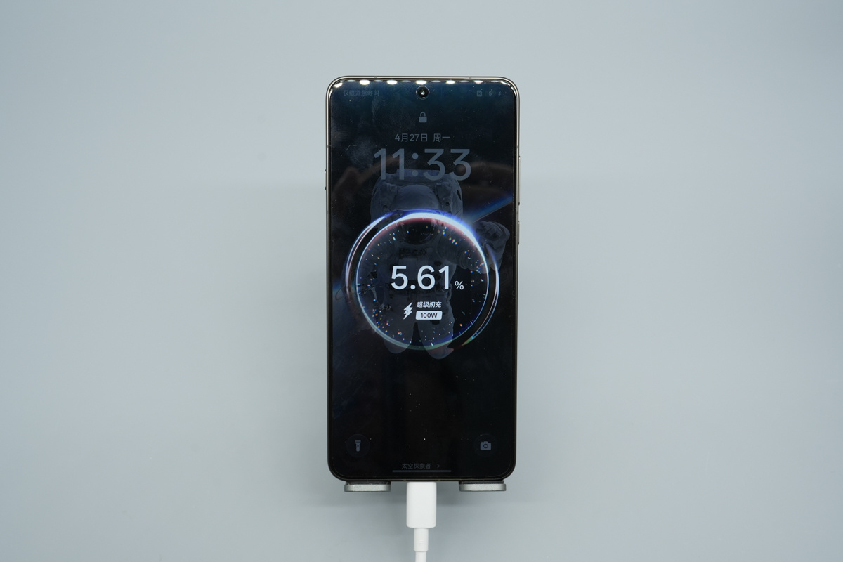
Connecting the OPPO Find X9 Ultra activates the 100W Super Flash Charge icon.
After a quick overview of the design and protocol support, let's dive into the actual product teardown.
Teardown
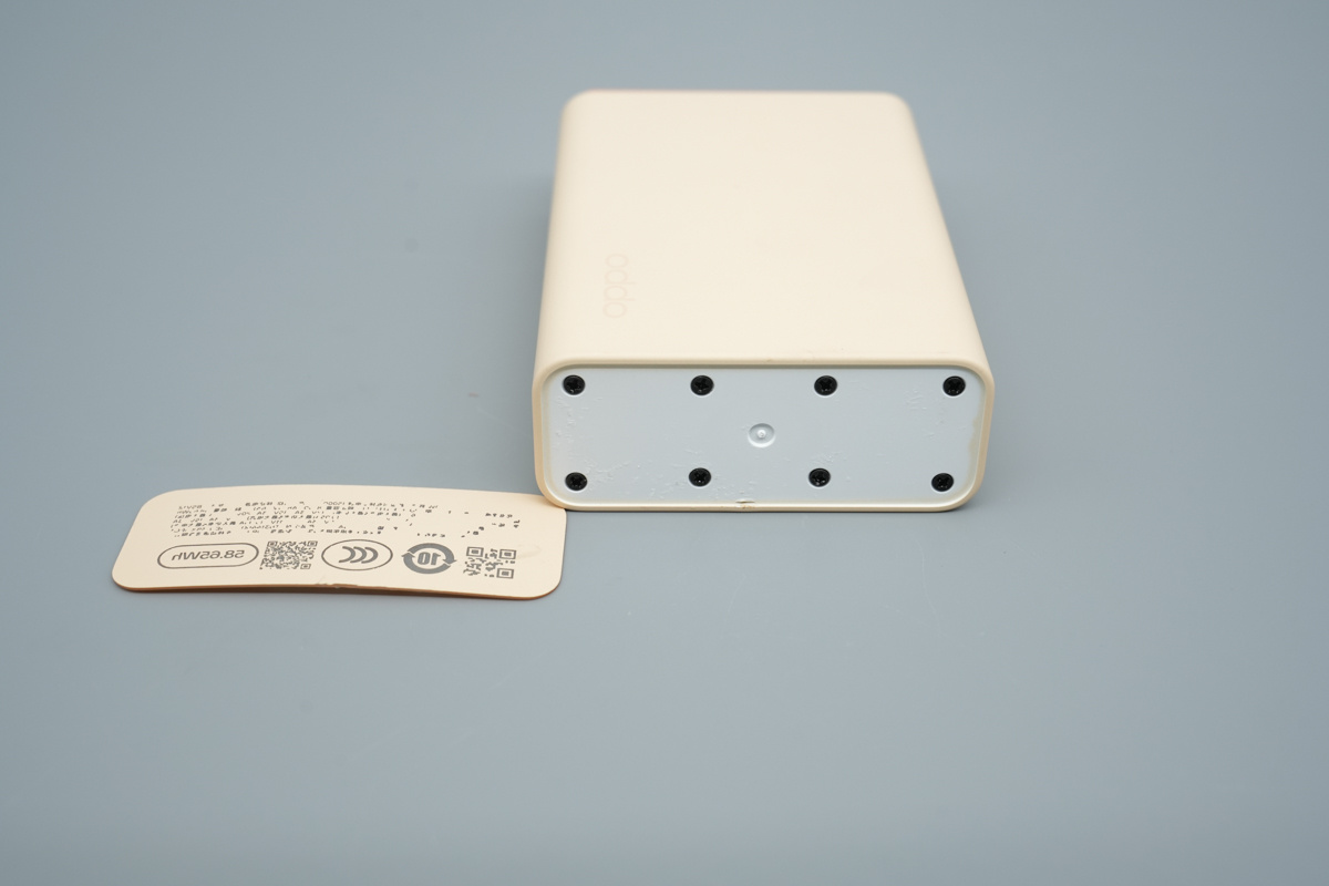
Prying off the bottom cover uncovers a series of Phillips screws hidden beneath it.
Next, we pry open the internal assembly from the orange top cover on the other end.
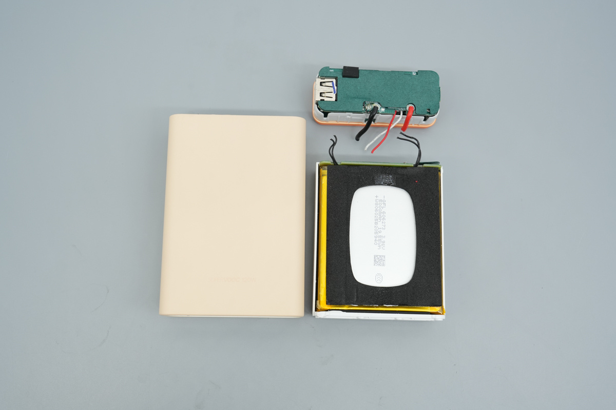
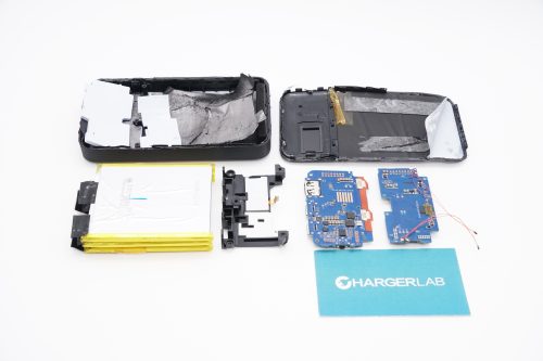
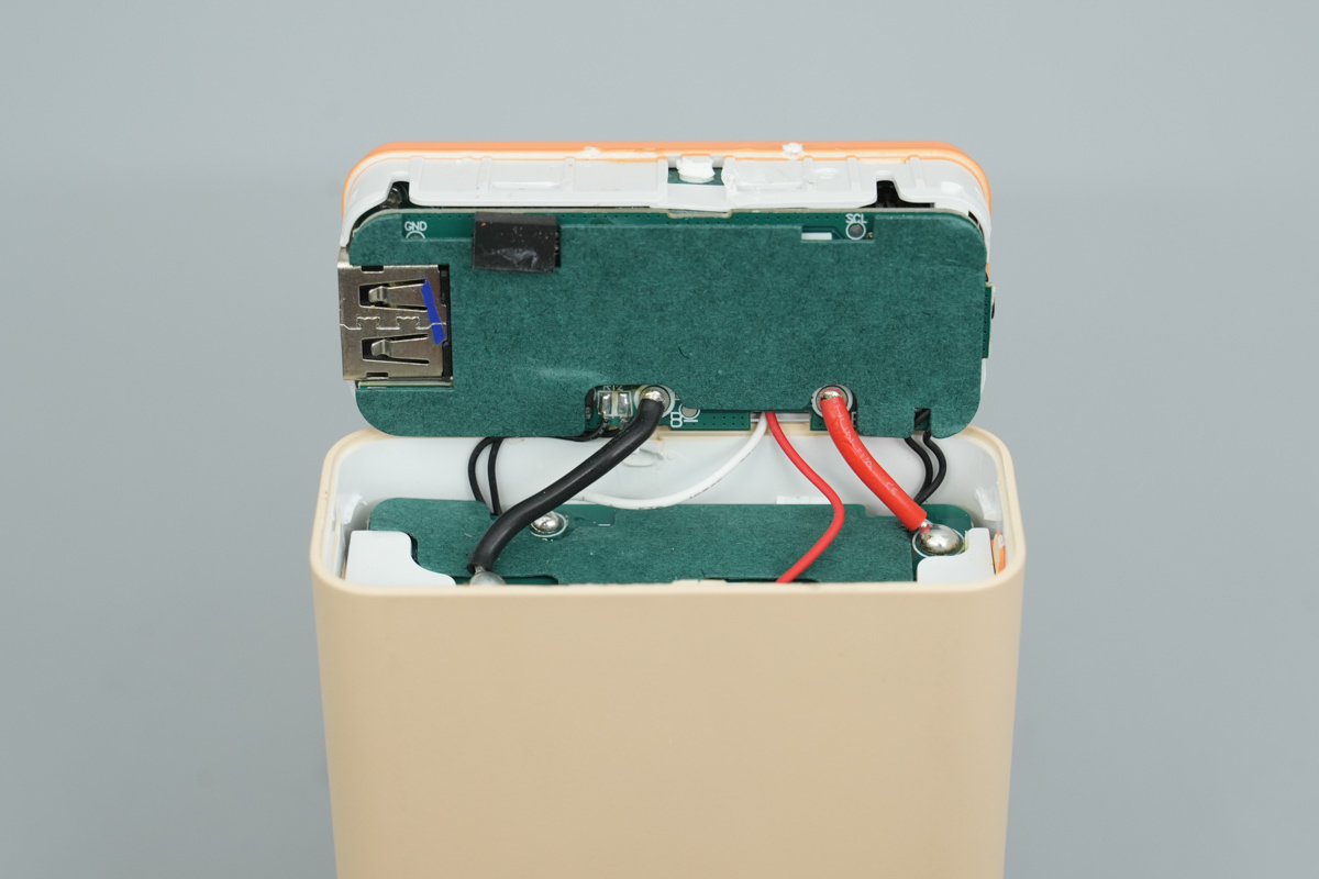
After unscrewing the base, the PCBA and battery pack can be pulled out from the top. The PCBA is linked to the battery by red/black power wires and two thermistors.
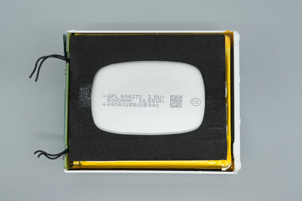
The battery pack, wrapped in black shock-absorbing foam, is housed in a white plastic protective frame.
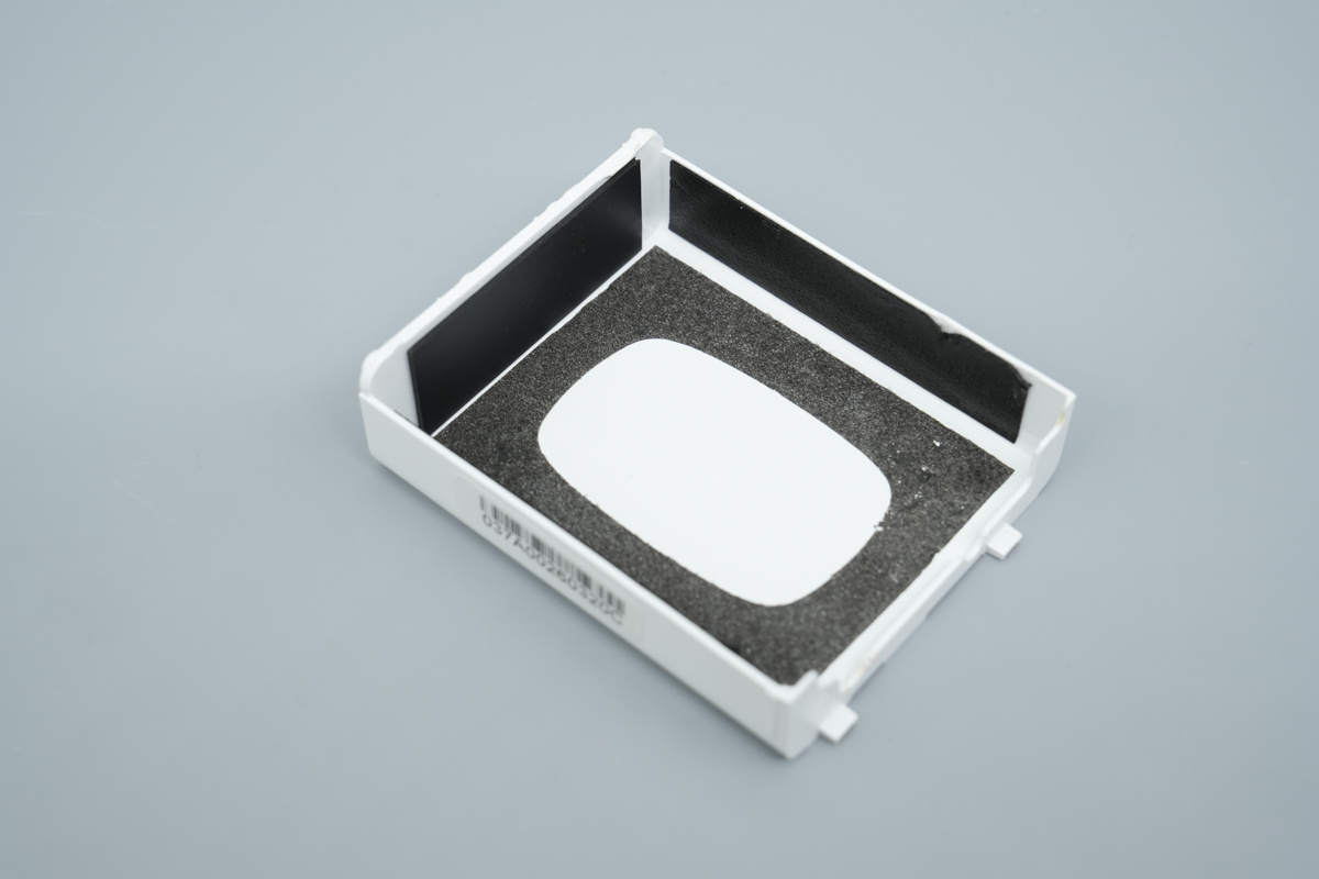
The white plastic frame housing the battery pack is lined on the inside with black insulating and shock-absorbing material.
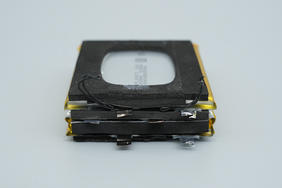
The battery pack features three series-connected lithium-polymer pouch cells, with the electrode tabs undergoing thorough insulation treatment.
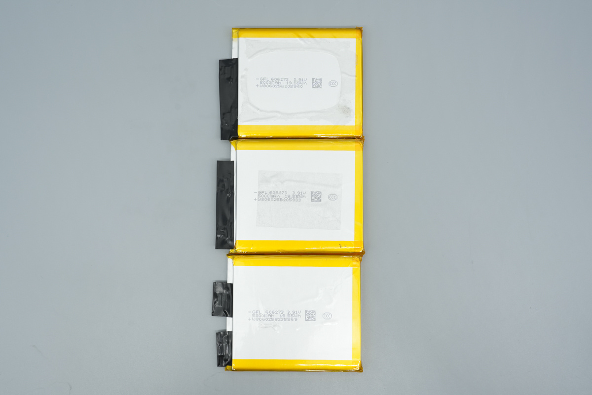
The three unfolded battery cells are identical in specs, providing the necessary foundation for high-power output.
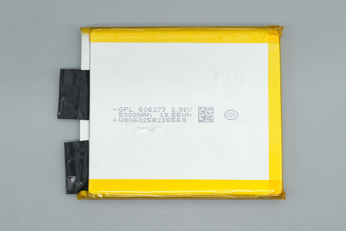
The battery cells are from GFL, spec 606273, 3.91V and 5,000mAh, and energy rating of 19.55Wh; the three cells provide a combined capacity of 15,000mAh.
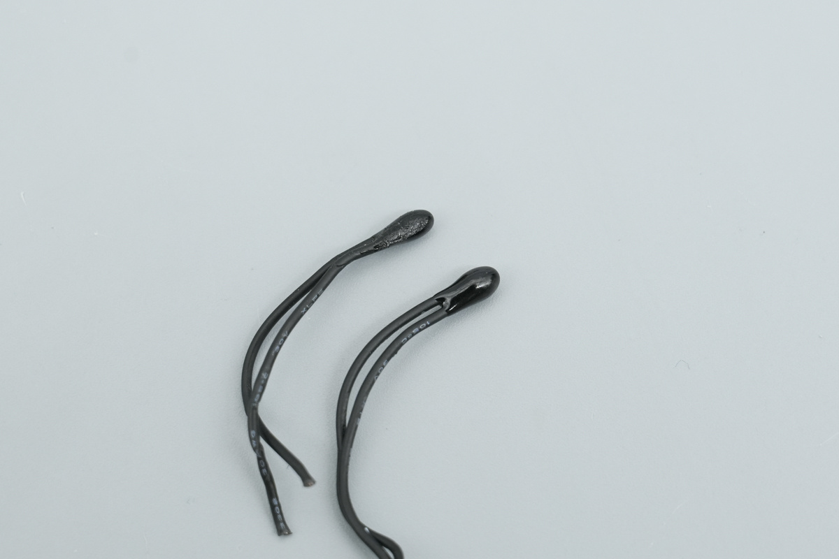
Two NTC thermistors are integrated within the battery pack for OTP.
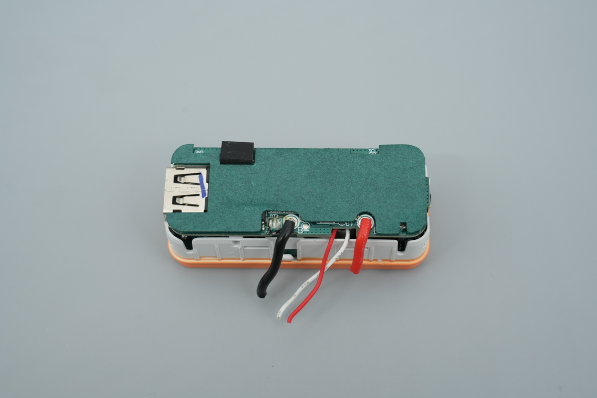
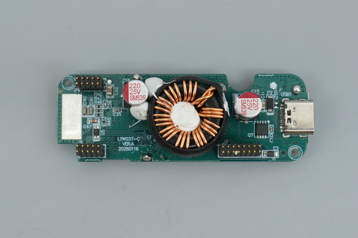
The rear of the top PCBA module is insulated with a full sheet of green fishpaper.
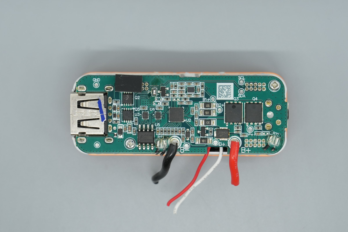
Removing the fish paper exposes the components on the PCBA module.
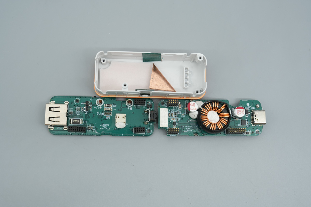
Removing the orange-and-white plastic cover reveals a stacked PCBA design using two pin-connected PCBs, with internal copper foil providing supplemental heat dissipation.
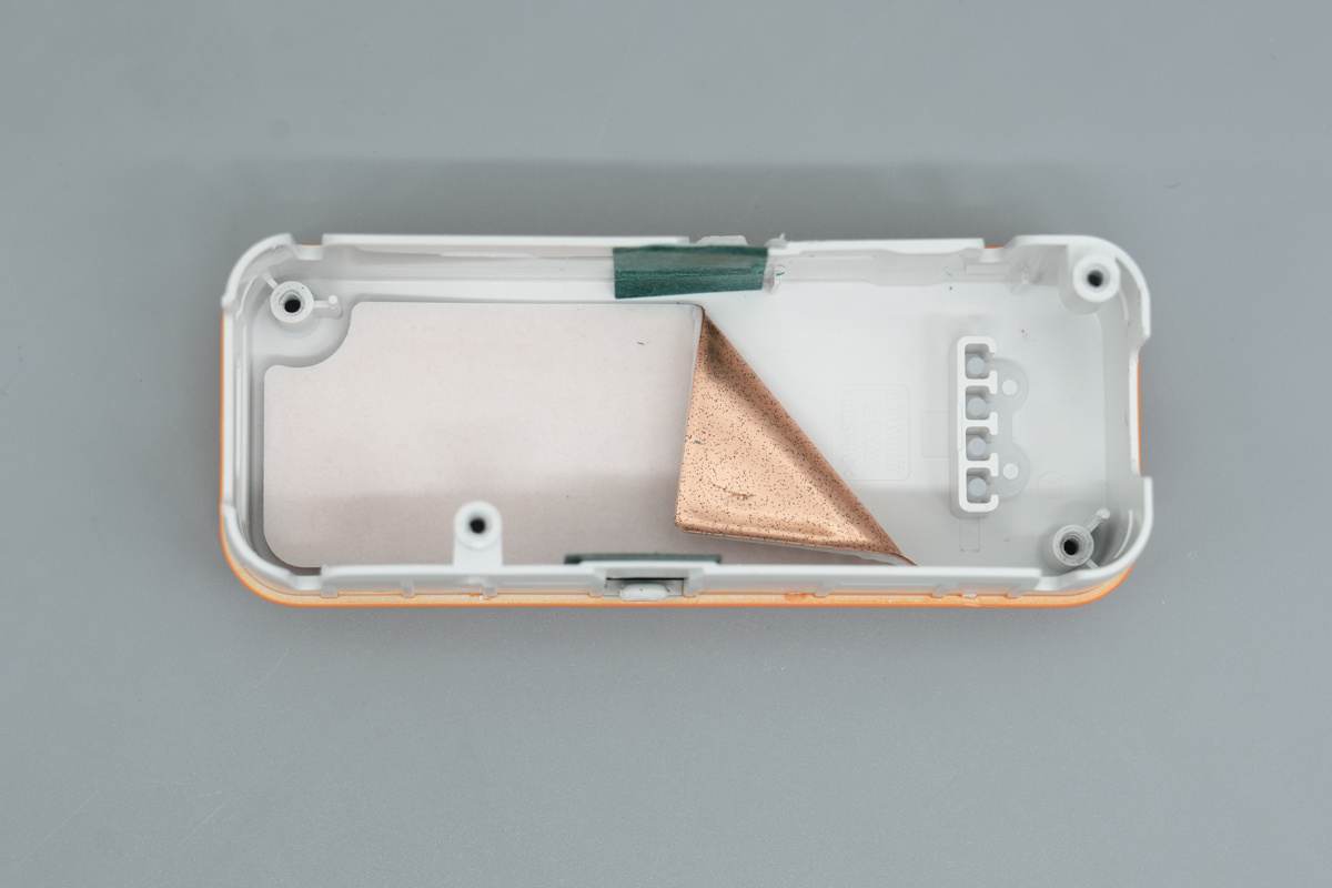
This is the internal copper foil heat sink, enabling rapid and uniform heat distribution.
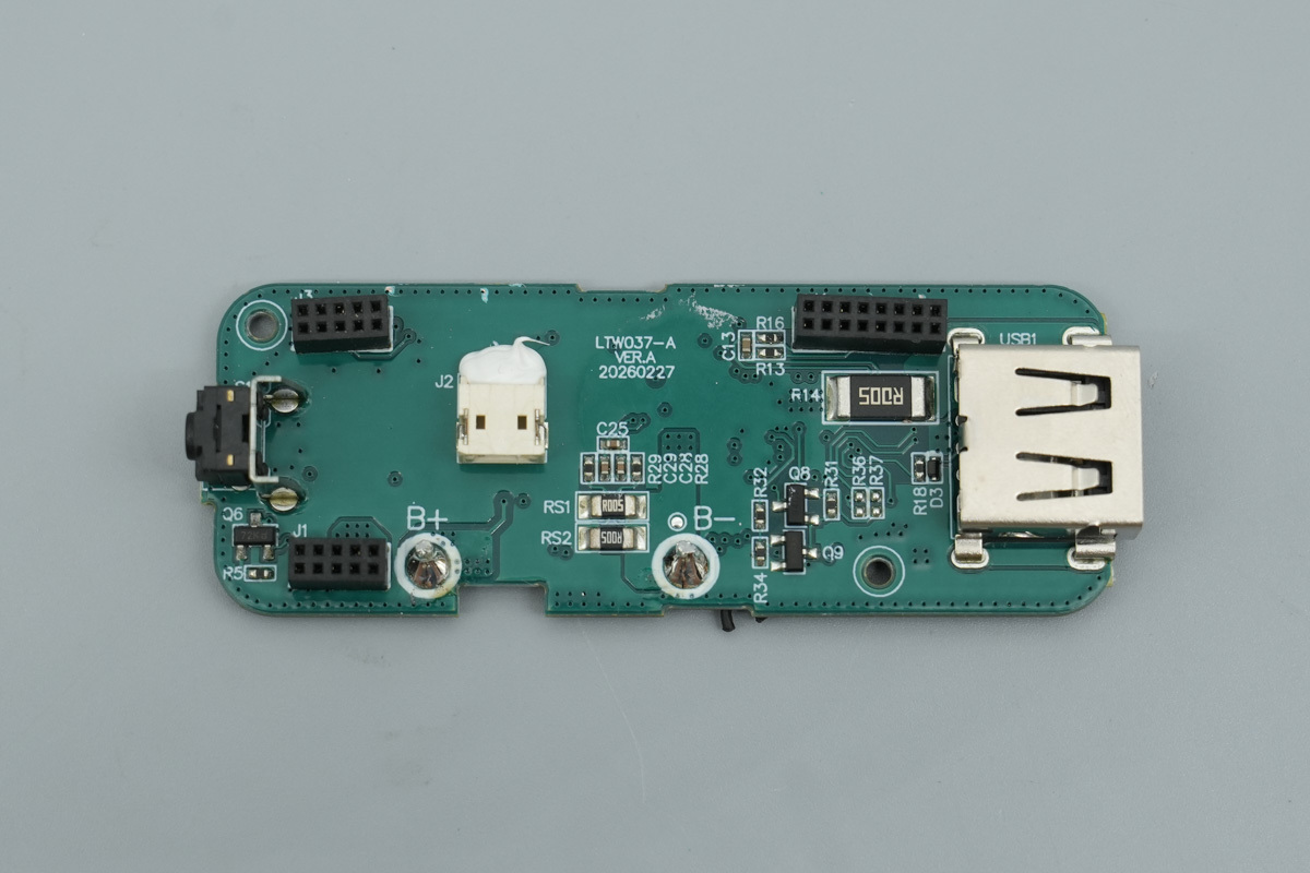
Separating the PCBs reveals the front of the bottom PCB, featuring a header connector, a power button, and a USB-A port.
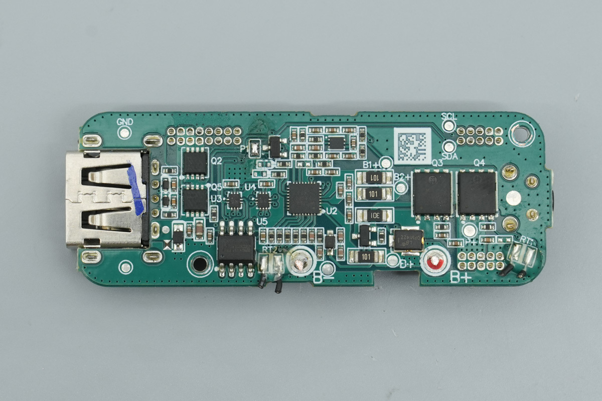
The back of the bottom board features the lithium battery protection chip, the USB to serial chip, and the lithium protection MOSFET and VBUS MOSFET.
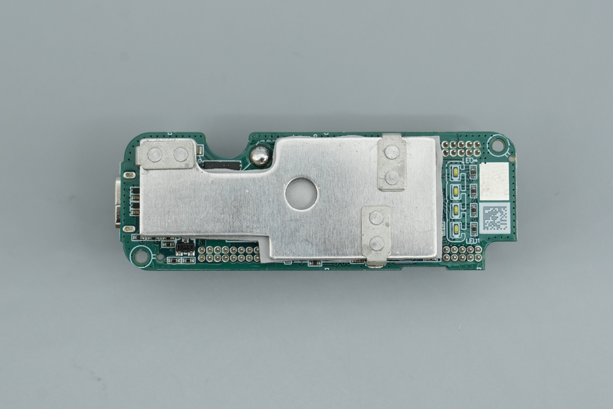
A silver metal shield covers the entire front of the top PCB to provide both shielding and heat dissipation.
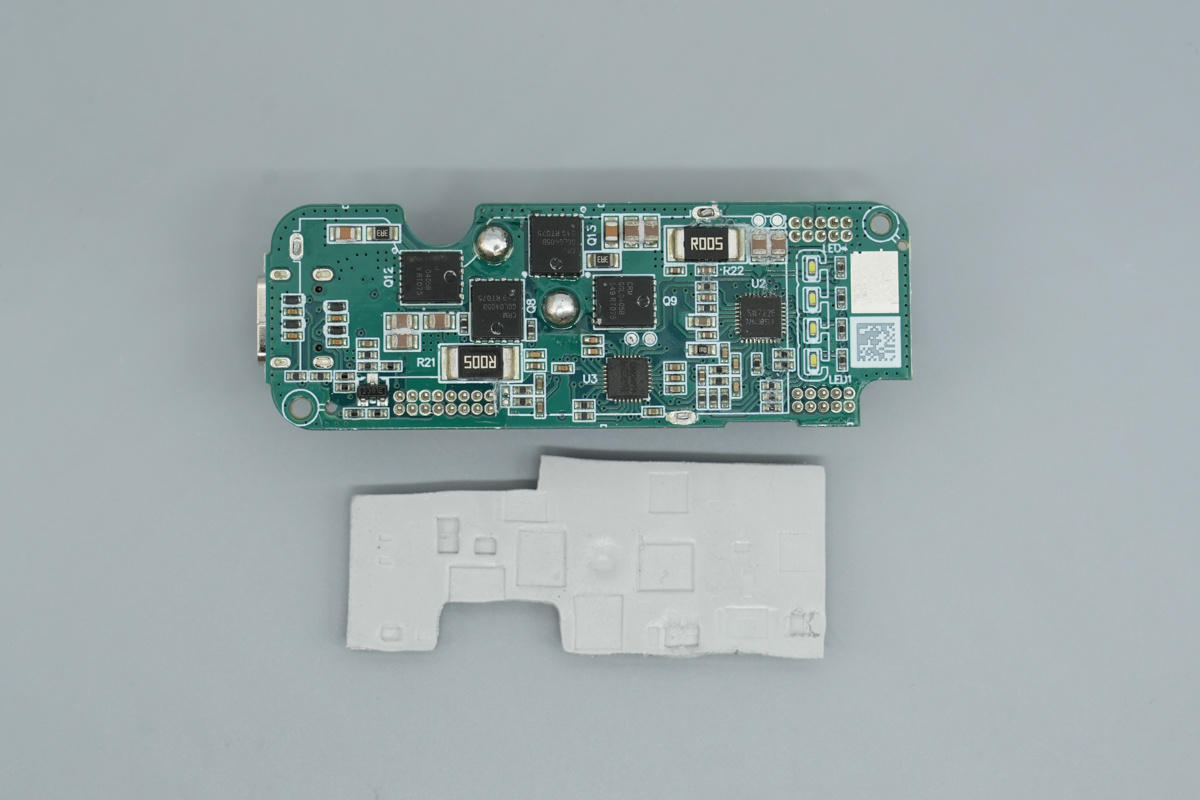
Removing the metal shield exposes a grey thermal pad underneath, used for auxiliary heat dissipation.
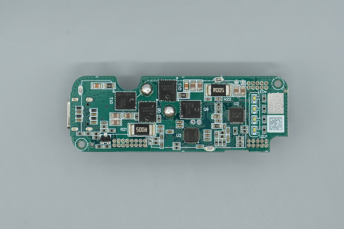
Removing the thermal pad reveals the bidirectional buck-boost chip, protocol chip, and several buck-boost MOSFETs.
The back side of the top PCB features the header pins, buck-boost choke, low-voltage filter caps, and the VBUS MOSFETs.
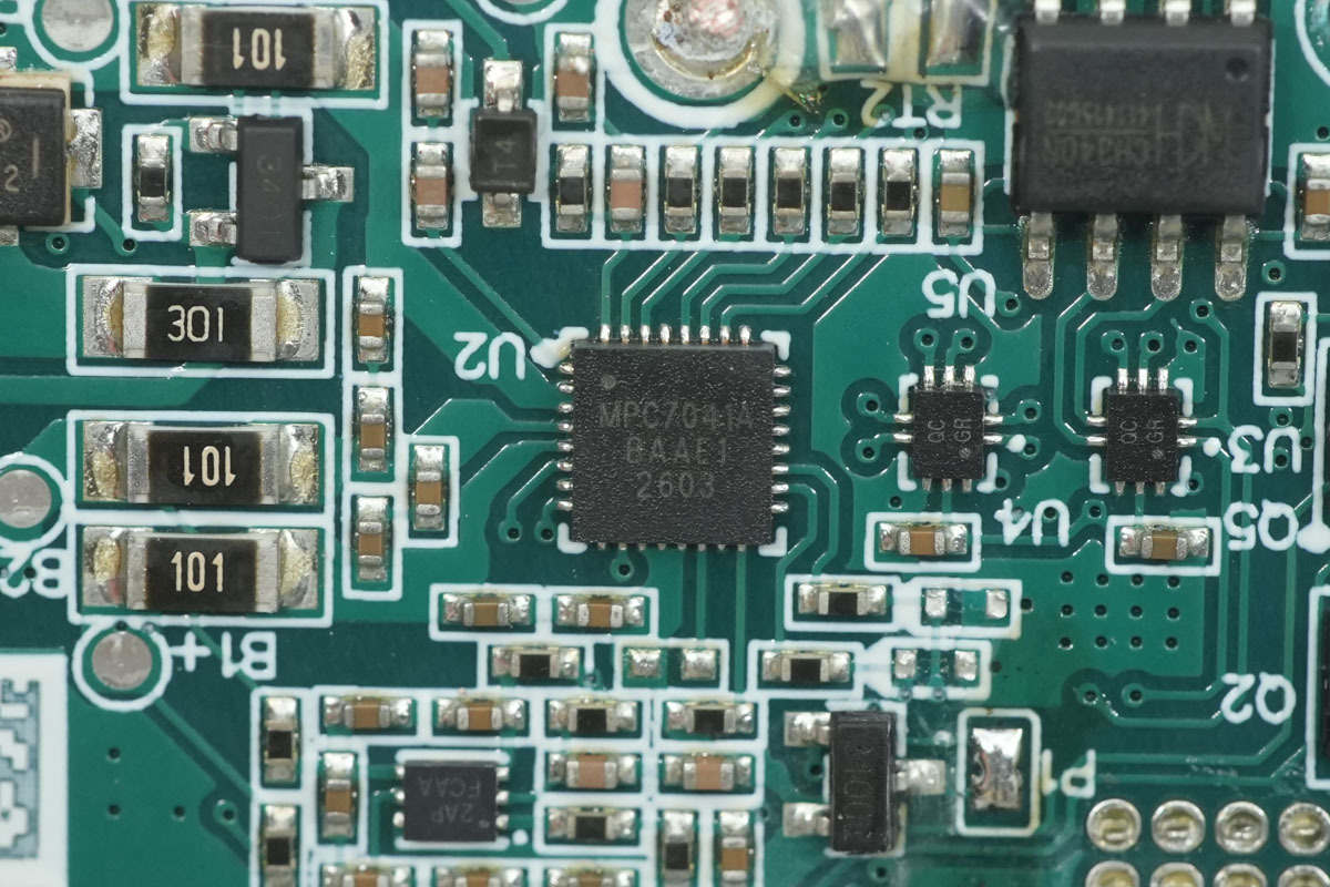
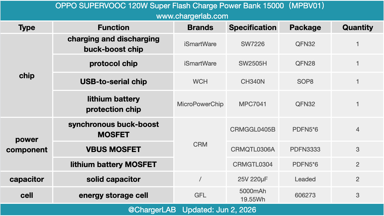
The lithium battery protection chip is from MicroPowerChip, model MPC7041, in a QFN32 package.
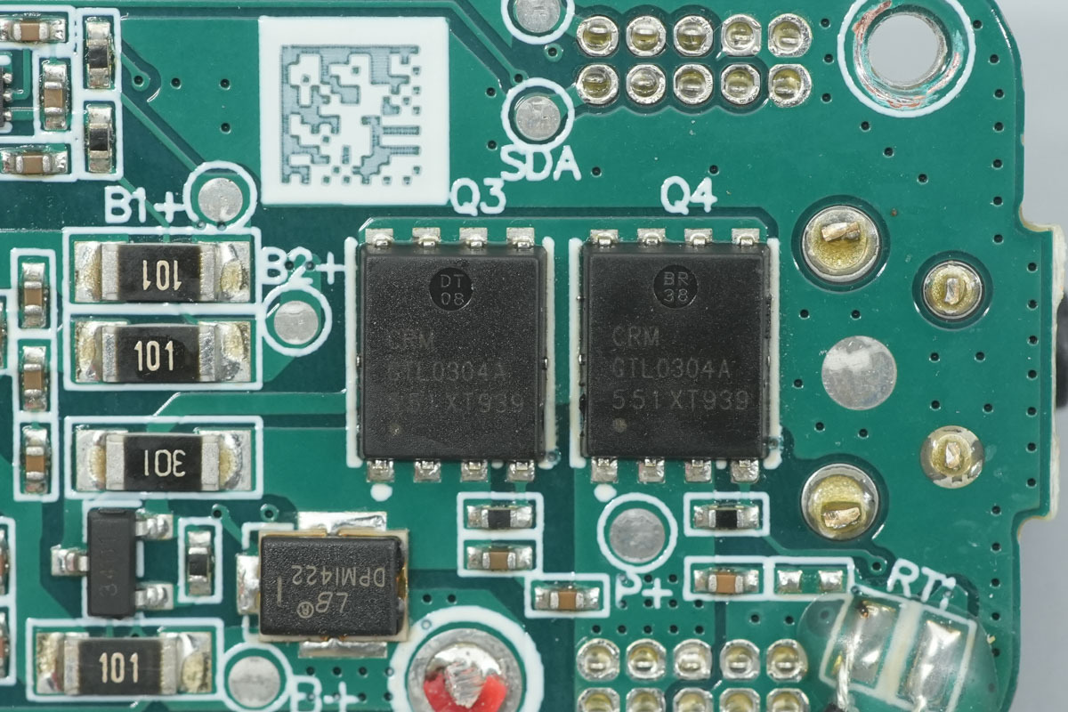
On the back of the bottom PCB, two lithium battery protection MOSFETs from CRM, model CRMGTL0304A, NMOS, 30V and 2.6mΩ, in a PDFN5*6 package.
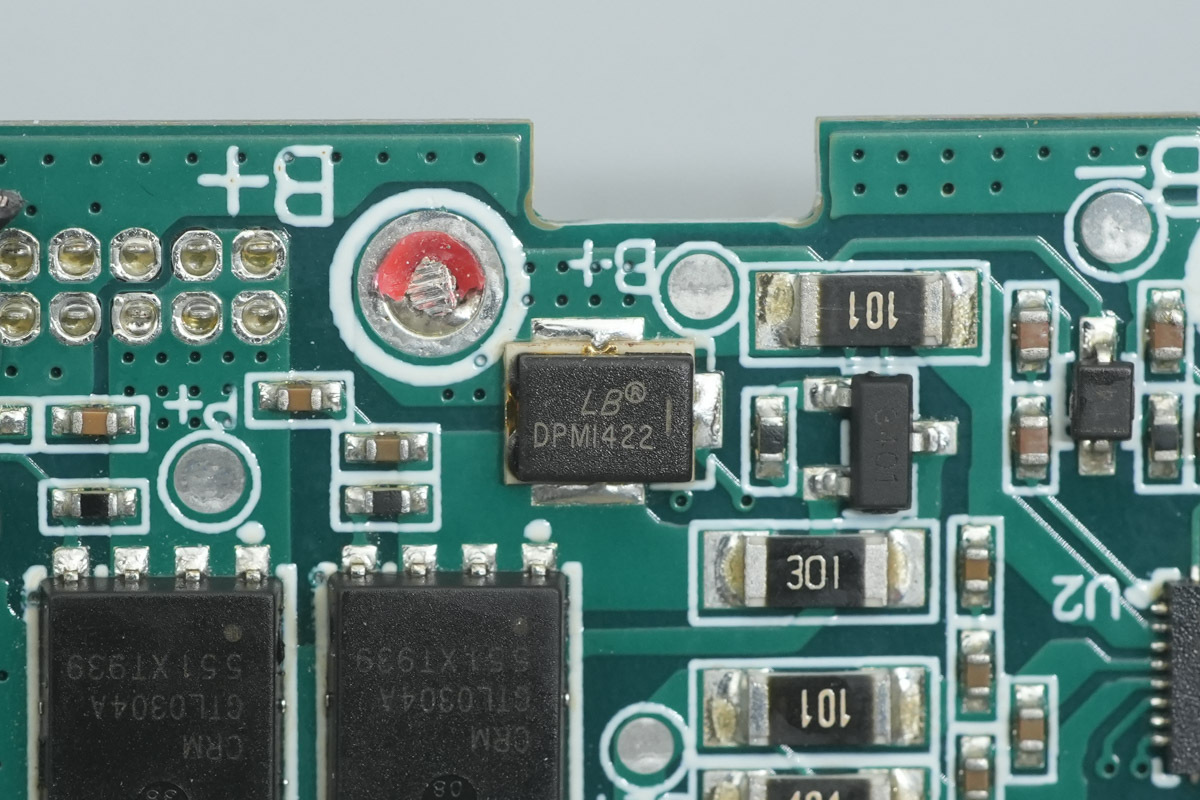
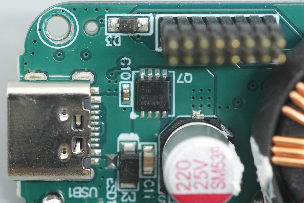
A chip, marked DPM1422.
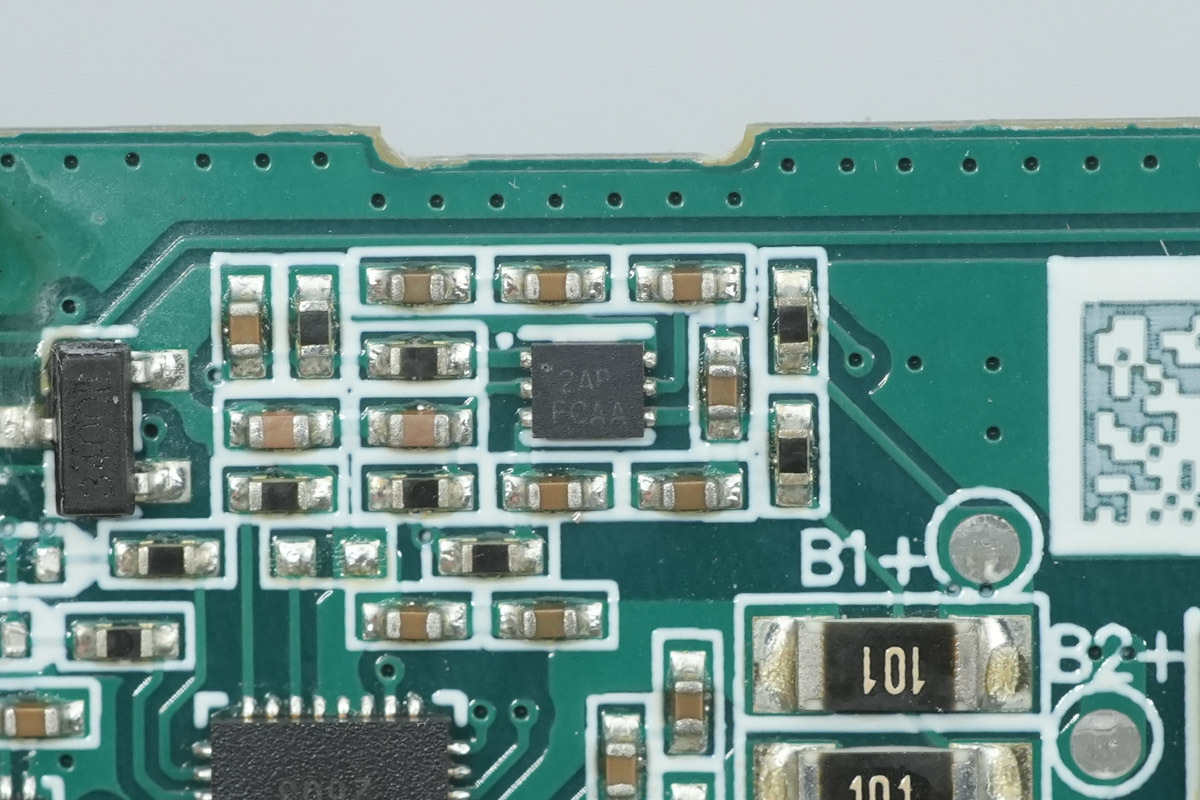
A chip, marked 2AP FCAA.
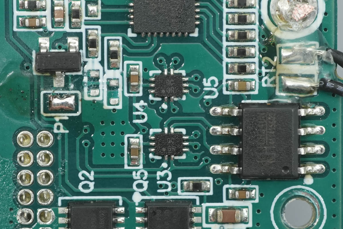
A MOSFET, marked QC GR, and additional peripheral driver components.
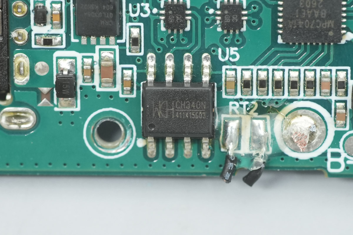
A USB-to-serial chip is from WCH, model CH340N, is integrated to facilitate communication functionality.
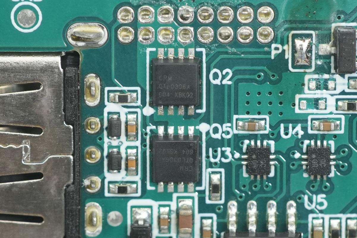
Two VBUS MOSFETs are from CRM, model CRMQTL0306A, 30V and 4.1mΩ, housed in a PDFN3333 package.
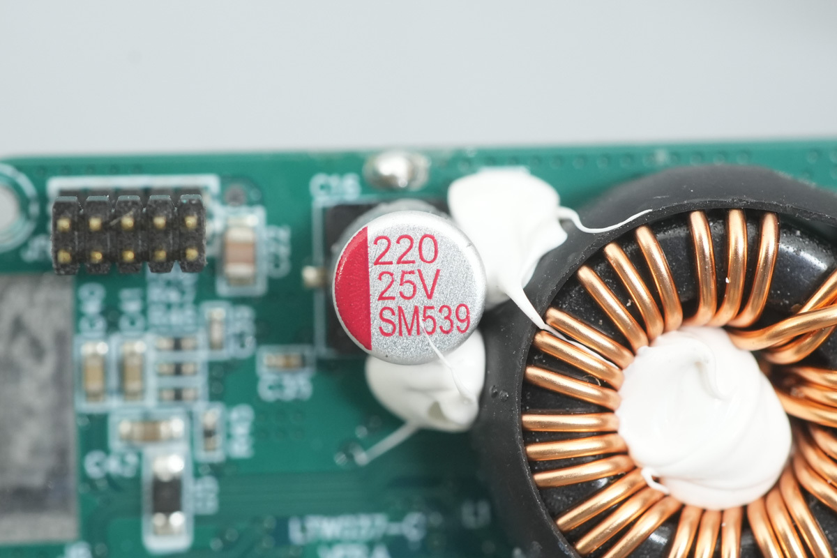
The top PCB features a 25V 220μF solid filter cap, fixed with white potting compound.
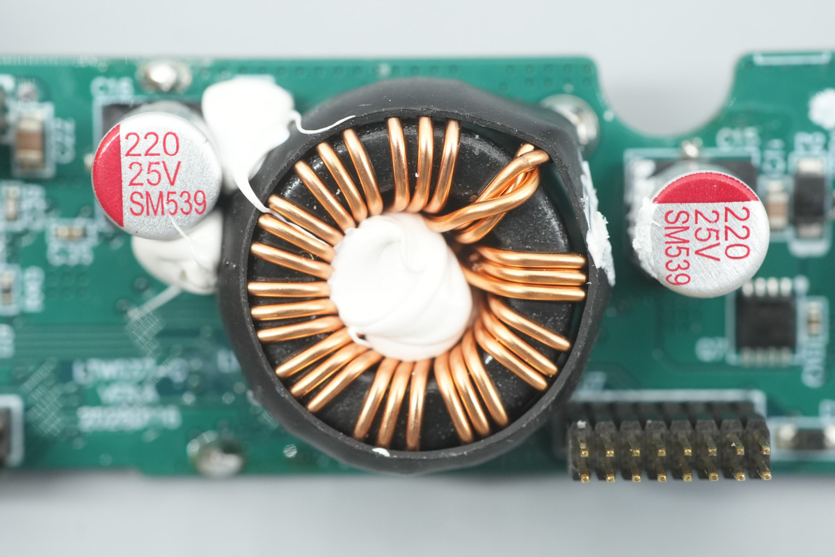
A buck-boost choke, features a multi-strand winding design, and secured by white potting compound in its center and perimeter.
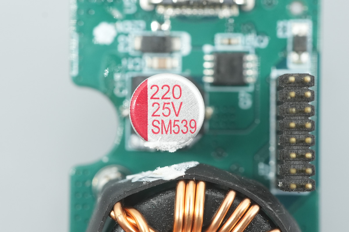
Another 220μF 25V solid cap is located on the opposite side of the choke, completing the output filter circuit.
The USB-C VBUS MOSFET is also from CRM, model CRMQTL0306A.
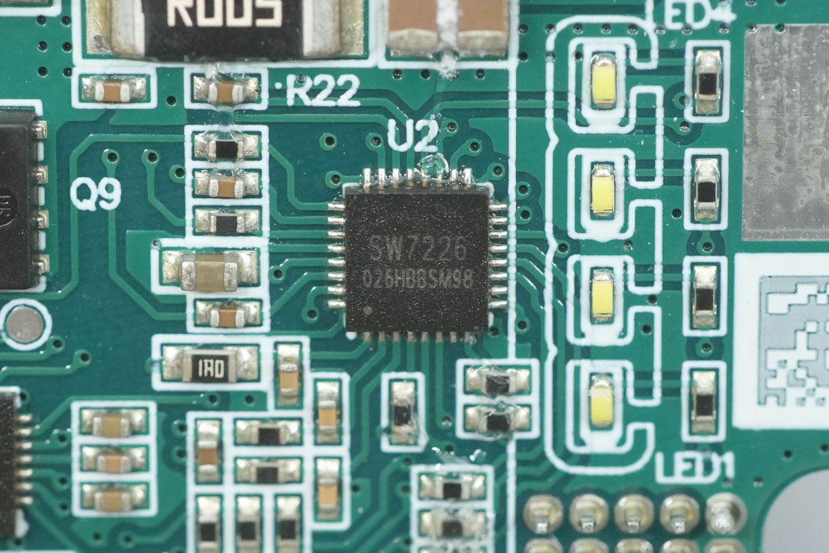
The bidirectional charging and discharging buck-boost chip located on the front of the top PCB is from iSmartWare, model SW7226, housed in a QFN-32 package. It is a high-efficiency synchronous bidirectional buck-boost controller compliant with the USB PD3.1 spec, specifically designed for mobile power banks, energy storage devices, power tools, electric toys, and other battery-powered equipment.
It supports input voltages up to 40V, is capable of charging 2-8 series ternary lithium batteries or 2-10 series LiFePO4 batteries, and provides a wide output voltage range from 3V to 37V, offering exceptional adaptability.
The SW7226 utilizes a Buck-Boost architecture capable of seamless switching between Boost, Buck, and Buck-Boost modes. It supports an adjustable switching frequency ranging from 200kHz to 500kHz, is compatible with 4.7µH and 10µH chokes, and allows for a 5mΩ sense resistor to enhance efficiency and precision.
In charging mode, it manages the complete process, including trickle, CC, CV, charge termination, and recharge. It supports precise I2C-controlled adjustments for target voltage (10mV increments) and charging current (50mA increments for input, 100mA for battery), complemented by adaptive current regulation to optimize efficiency and battery longevity.
During discharge, it provides a wide output voltage range of 3V to 37V. It supports I2C control for voltage and current and utilizes FB feedback for output voltage regulation to meet USB PD3.1 standards. Furthermore, the chip features an integrated 12-bit ADC for real-time voltage and current monitoring, ensuring high system stability and efficiency.
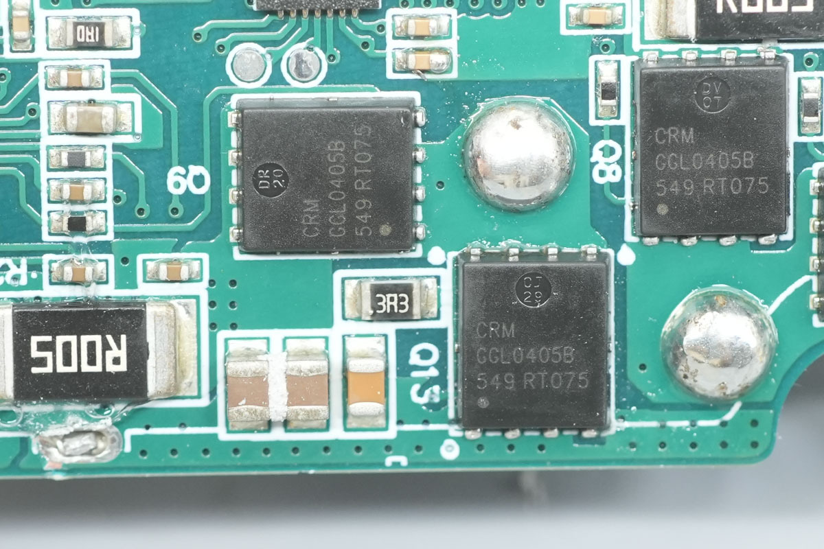
The synchronous buck-boost MOSFETs are from CRM, model CRMGGL0405B, 40V and 4.6mΩ, in a PDFN5*6 package.
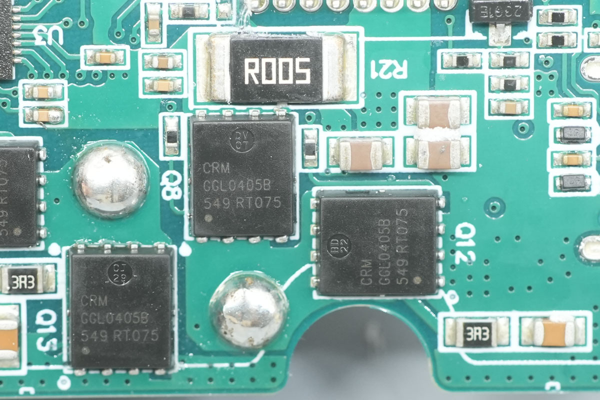
Another one is also from CRM, model CRMGGL0405B, four synchronous buck-boost MOSFETs in total.
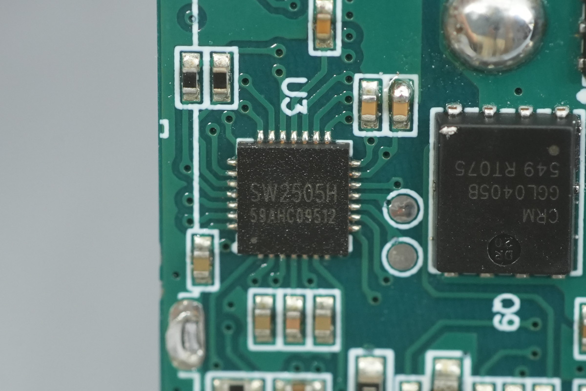
The protocol chip is also from iSmartWare, model SW2505H. This is a low-power controller chip featuring comprehensive protocol support, including USB PD3.1, QC, and UFCS. It is certified for USB PD3.1 EPR, supports DRP mode, and integrates an MCU with 16 GPIOs. Furthermore, it supports online firmware upgrades, in-circuit simulation and debugging, and provides flexible control interfaces, including optocoupler, FB feedback, and I2C (both master and slave modes).
The SW2505H features a high-efficiency 40MHz Cortex-M0 processor, ample Flash and SRAM memory, and versatile communication interfaces (I2C, UART) alongside robust GPIO and GPADC support. Its low-power design supports precise output regulation from 3.3V to 32V and current limiting from 0.3A to 12A.
Beyond core processing, it incorporates advanced feedback control mechanisms and bus voltage monitoring. It integrates CV and CC control loops, fast VIN/VBUS discharge circuitry, and dedicated NMOS gate drivers, ensuring a highly stable and reliable power management architecture.
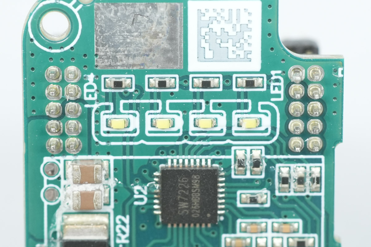
Four LED indicators is implemented to provide battery level status display.
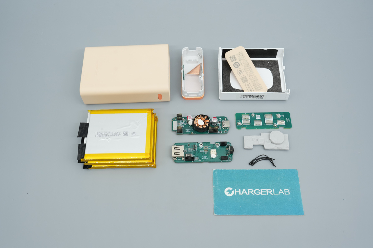
Well, those are all components of the OPPO SUPERVOOC 120W Super Flash Charge Power Bank 15000.
Summary of ChargerLAB
The OPPO SUPERVOOC 120W Super Flash Charge Power Bank combines a vibrant beige-and-orange aesthetic with a sleek, ergonomic build.
Packed with a 15,000mAh capacity, this power bank delivers OPPO’s signature 120W fast charging while maintaining compatibility with universal standards like PD and UFCS. It also introduces smart health monitoring to provide users with real-time status updates, ensuring safer daily operation.
Inside, it features a dense, two-PCB stacked architecture. Core management is handled by iSmartWare’s SW7226 buck-boost chip and SW2505H protocol chip, with MicroPowerChip providing the battery protection. Power path components—including the synchronous buck-boost, VBUS, and protection MOSFETs—are supplied by CRM.
Safety is a priority, the battery cell is encased in shock-absorbent foam and a rigid plastic frame. The PCBA is bolstered by metal shields and thermal pads, further supported by large copper foil sections on the inner shell and dual NTC thermistors. This premium internal configuration guarantees reliable performance even at 120W output.
Related Articles:
1. Teardown of OPPO 120W SuperVOOC GaN Charger (OSABBCBBAC)
2. Review of OPPO 100W SUPERVOOC GaN Charger
3. OPPO Launches Multiple Magnetic Accessories