Introduction
Established in 2013, HONOR has evolved into a flagship tech brand focused on delivering a seamless, all-channel ecosystem for global consumers. With a vast product range including smartphones, tablets, wearables, smart home gear, and laptops, HONOR is committed to crafting the ultimate technological lifestyle.
Following our previous teardown of the HONOR 35W original fast charger, ChargerLAB has now secured the HONOR 45W US Original Fast USB-A charger.
Adopting the brand's signature aesthetic, this charger features fixed US pins and a single USB-A interface. It is compatible with QC2.0, FCP, SCP, and DCP protocols, enabling a peak power output of 45W (11V/4.1A). Tailor-made for the Huawei and HONOR device ecosystem.
We are now conducting a thorough teardown to inspect the high-quality engineering and components housed within.
Product Appearance
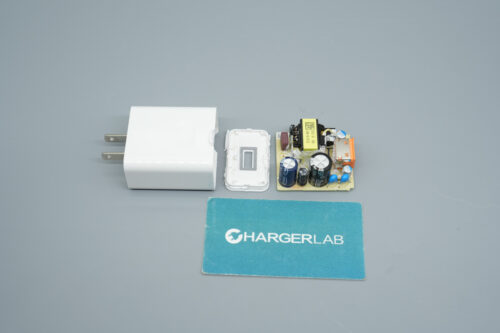
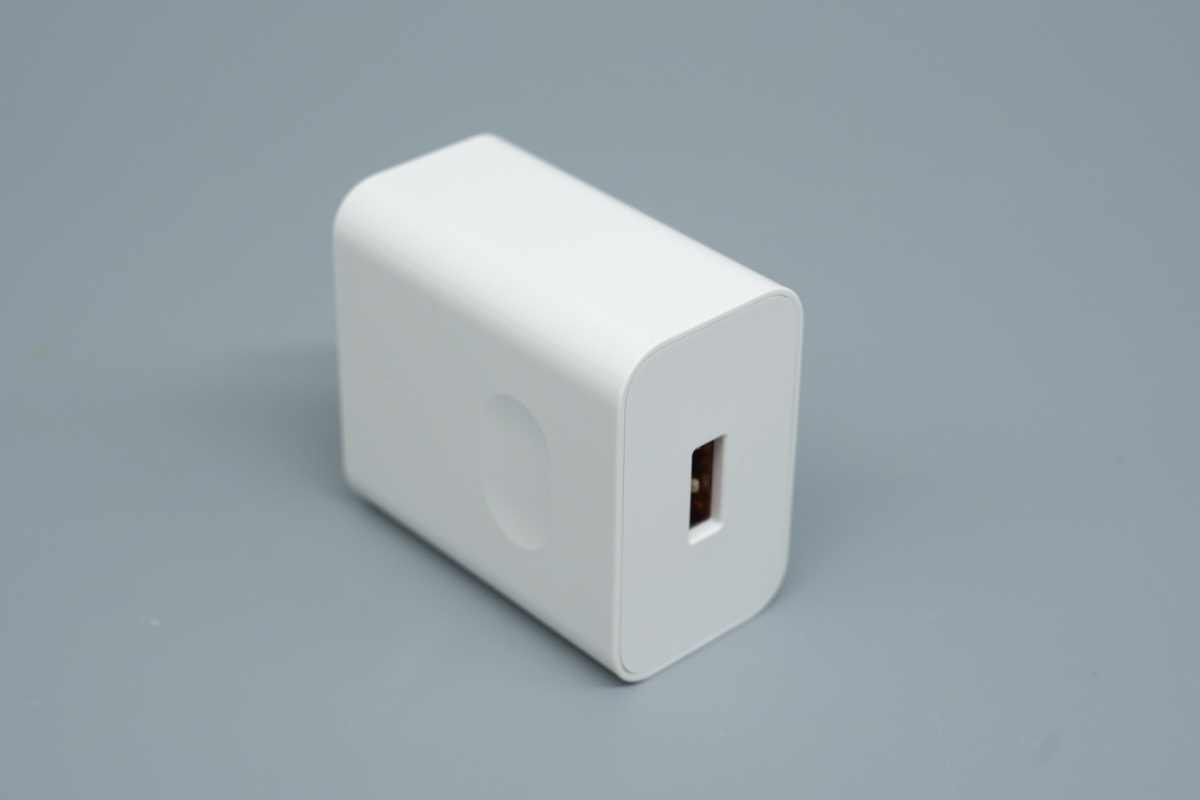
The charger features a white, flame-retardant PC casing with rounded edges for a smooth transition. Both sides of the housing are designed with elliptical recesses to provide a secure grip during insertion and removal, and it is equipped with fixed input pins.
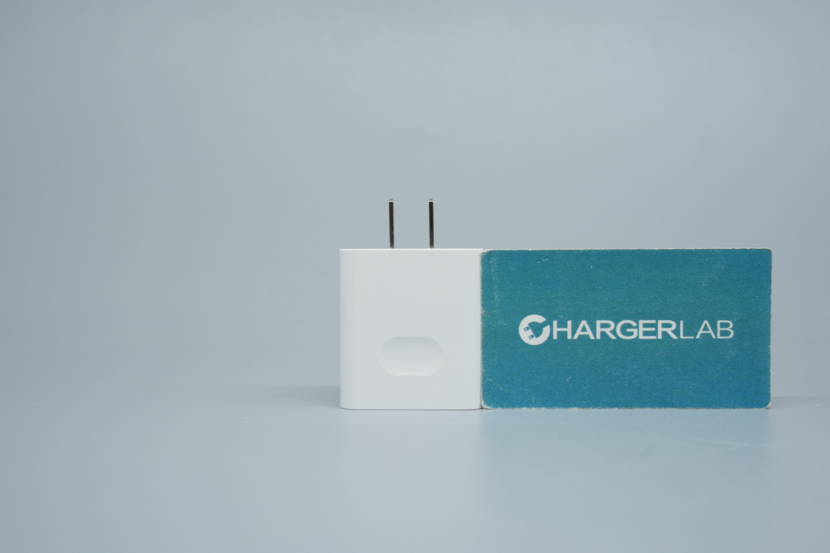
The metal prongs feature circular holes, which are a classic design feature of standard US-type plugs.
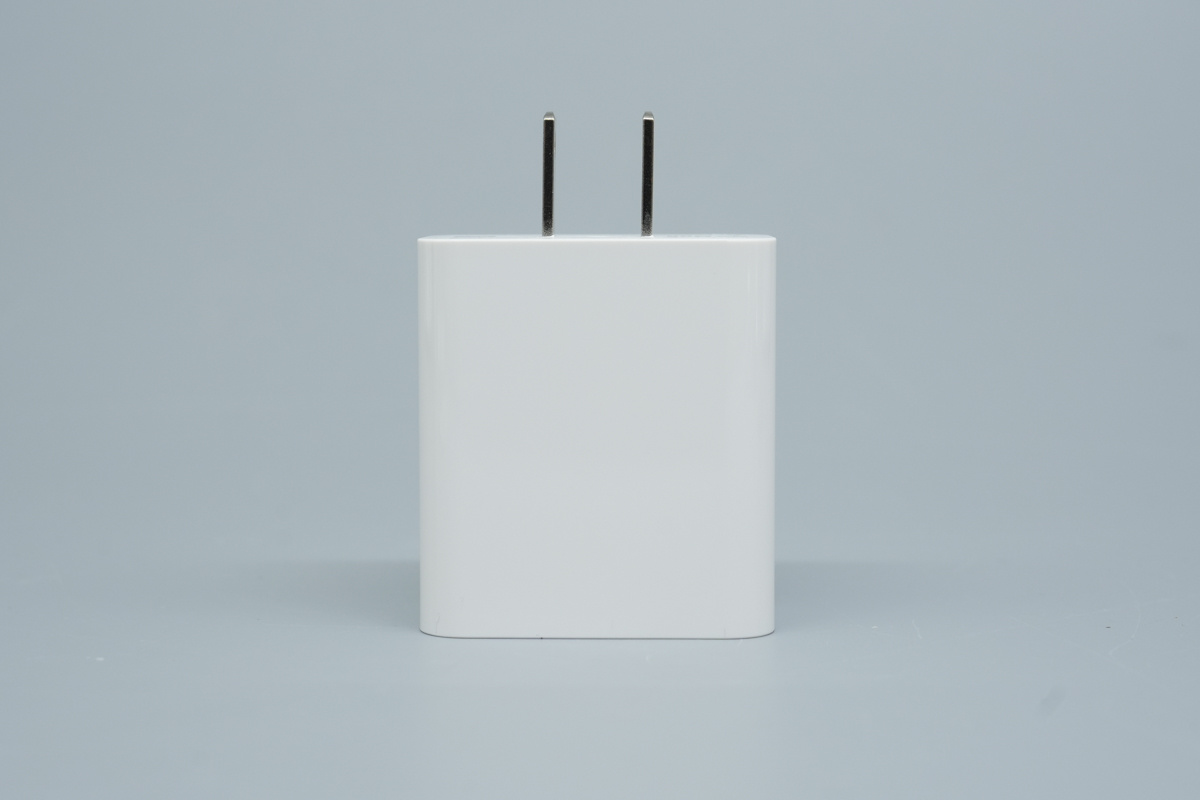
It’s side profile design is remarkably minimalist and clean.
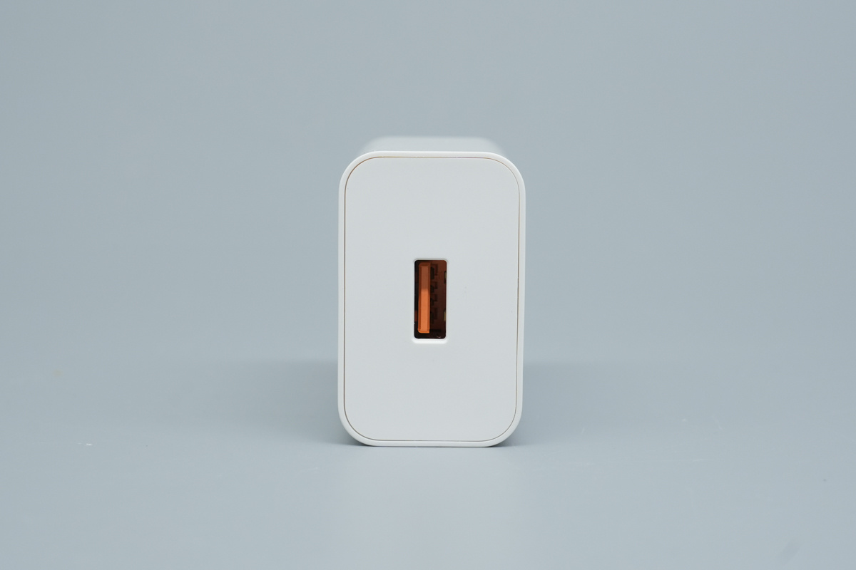
The output end of it features a flat design and a single USB-A port, which utilizes the brand's iconic orange internal plastic sheet.
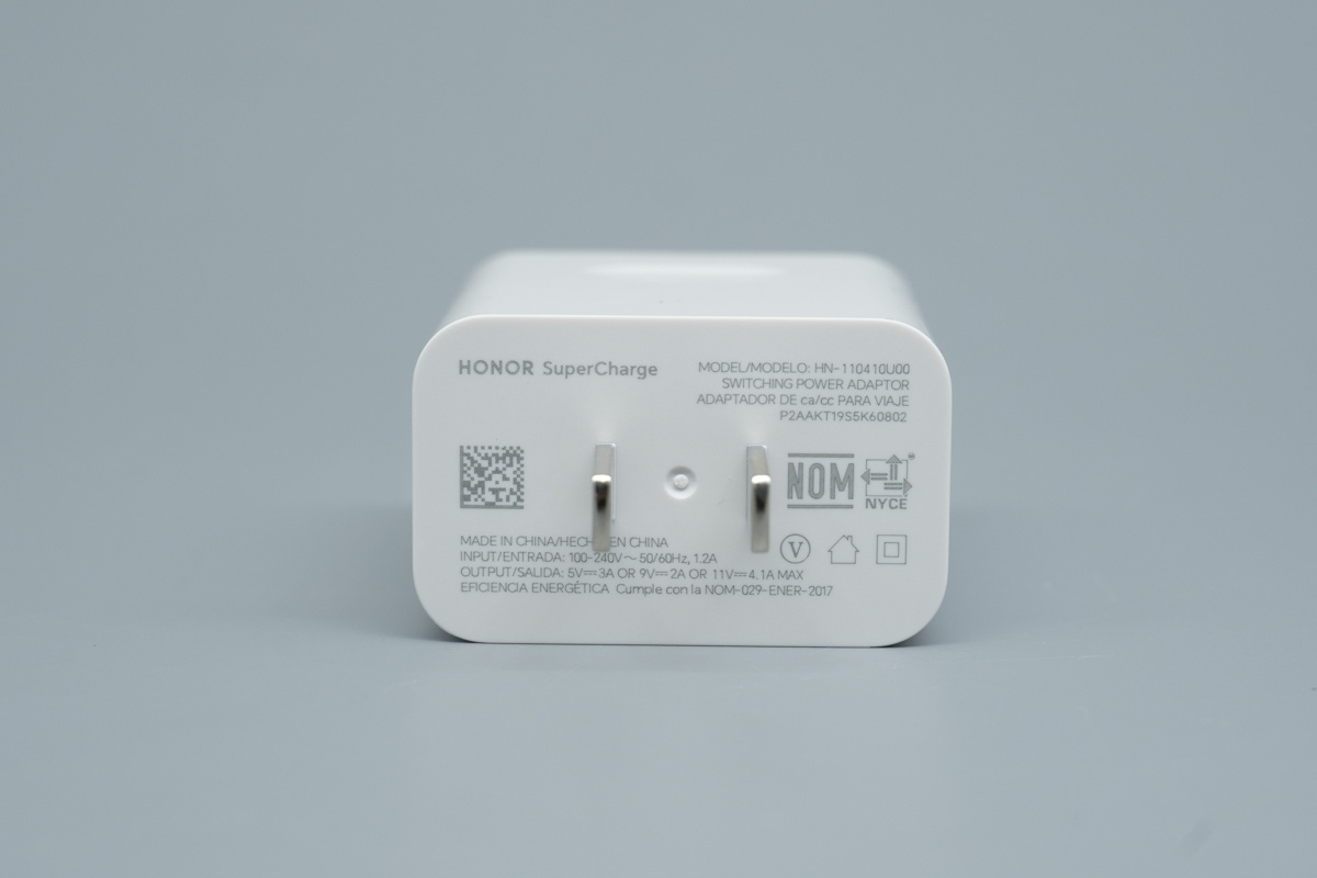
The input pin section clearly displays the charger’s technical specs:
Model: HN-110410U00
Input: 100-240V~ 50/60Hz 1.2A
Output: 5V=3A, 9V=2A, or 11V=4.1A MAX
Certifications: NOM, NYCE, and Level VI energy efficiency.
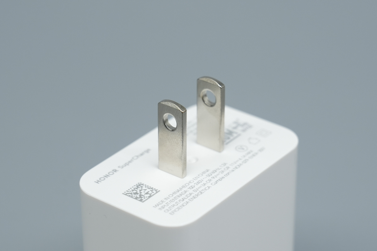
The US pins exhibit high-quality manufacturing, featuring clean, burr-free edges.
It’s output end features refined craftsmanship with seamless, uniform construction throughout.
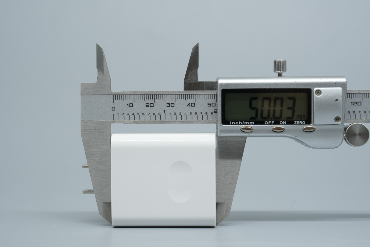
The length of the charger is about 50.03mm (1.970 inches).
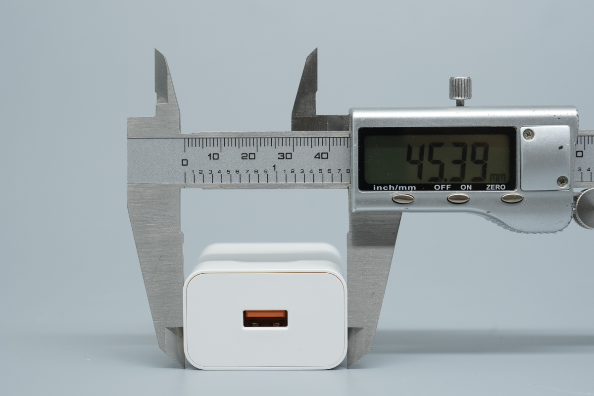
The width of the charger is about 45.39mm (1.787 inches).
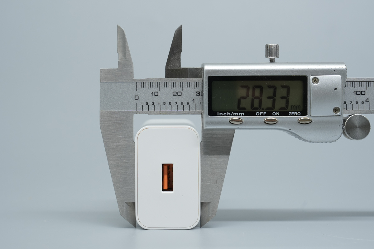
The thickness of the charger is about 28.33mm (1.115 inches).
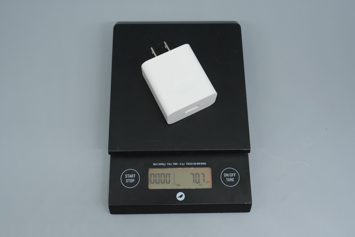
The weight is about 70.7g (2.49 oz).
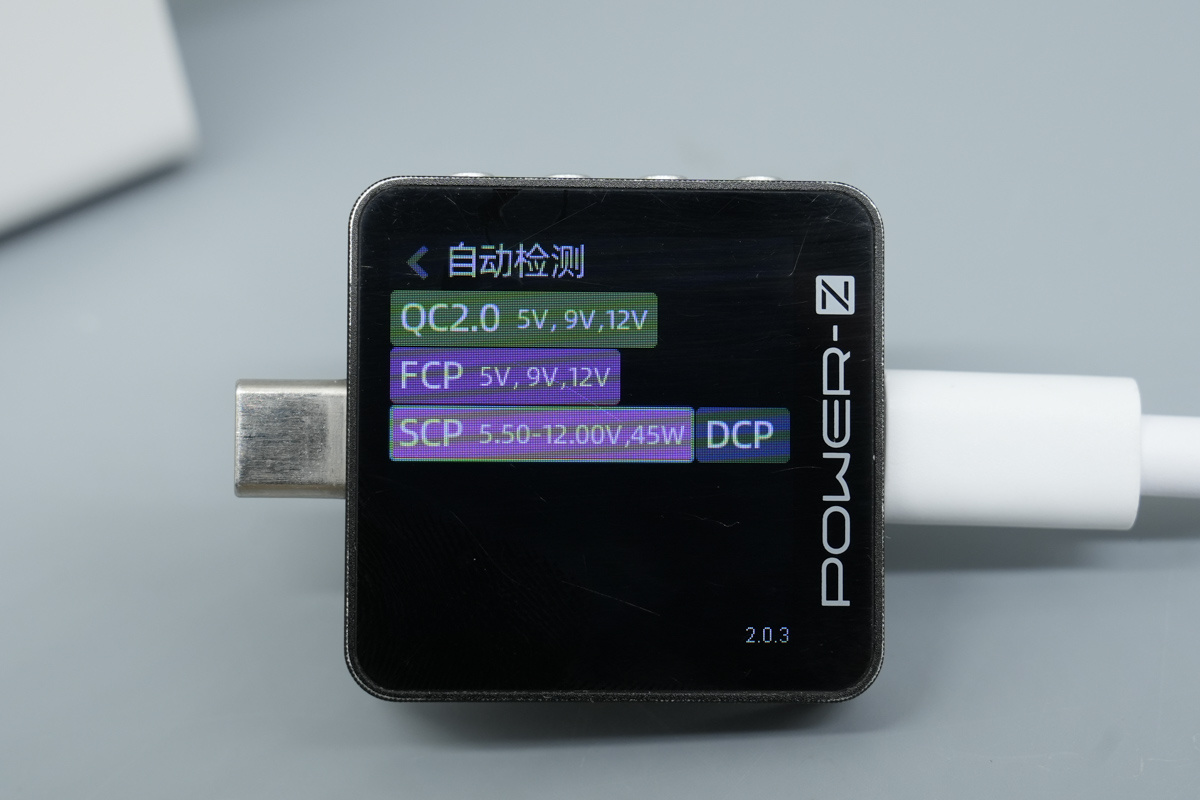
ChargerLAB POWER-Z KM003C shows that the USB-A port supports QC2.0, FCP, SCP and DCP.
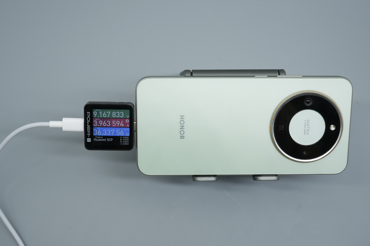
Testing with the HONOR X70 confirmed the charger’s capabilities, reaching 36.33W (9.16V/3.96A) and successfully triggering the SCP fast-charging protocol.
After a quick look at the design and functional test, it’s time for us to dive into the teardown here at ChargerLAB.
Teardown
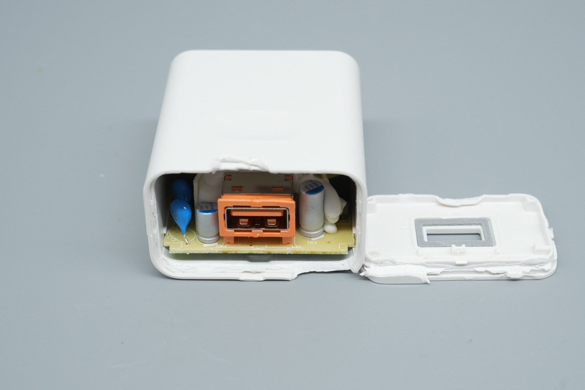
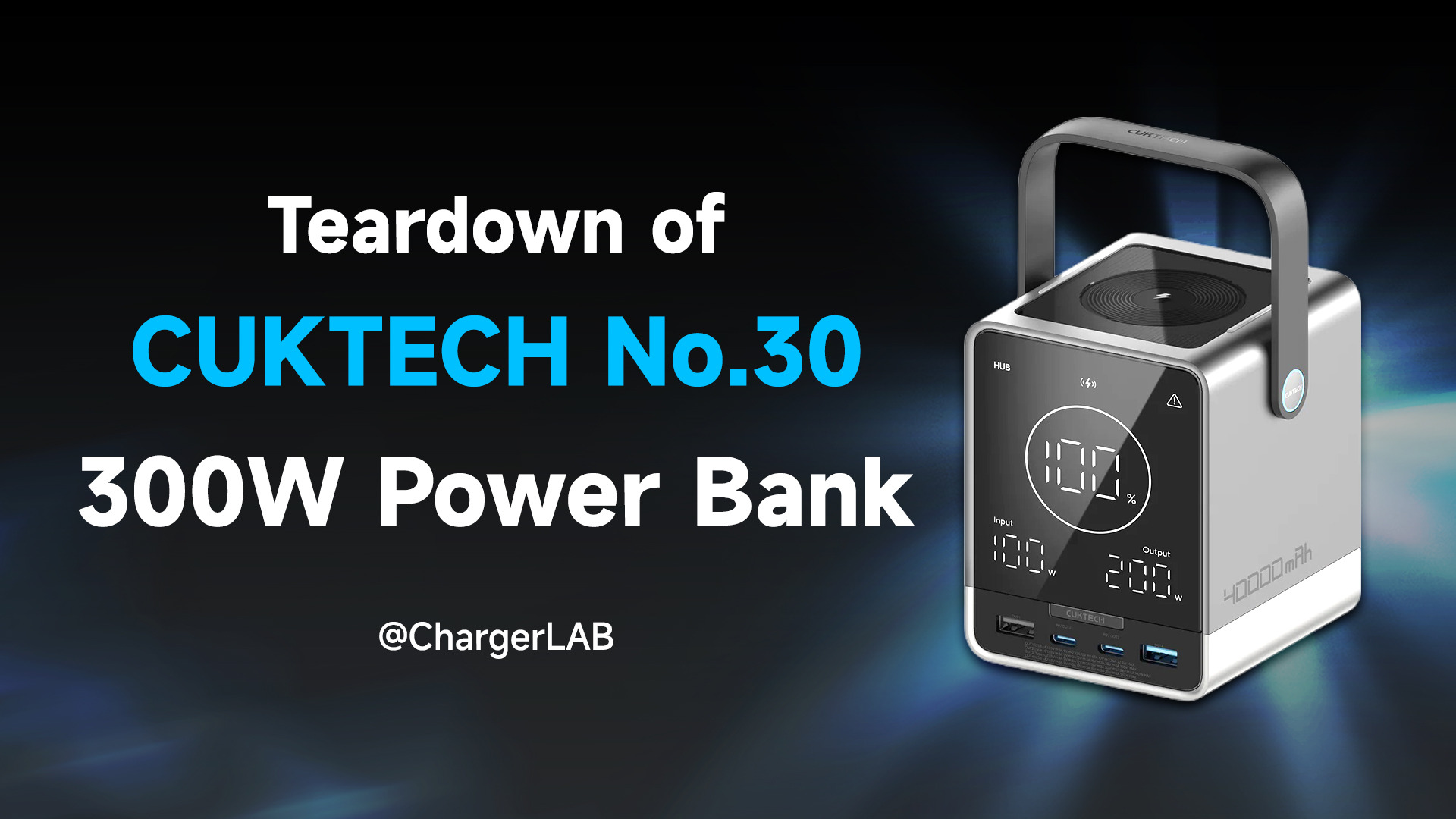
The outer casing is opened by prying along the ultrasonic welding seam at the output panel.
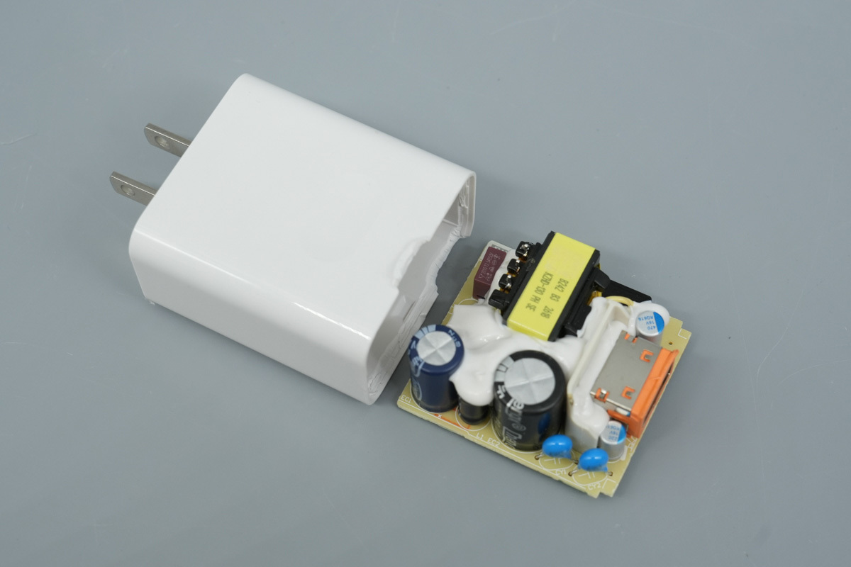
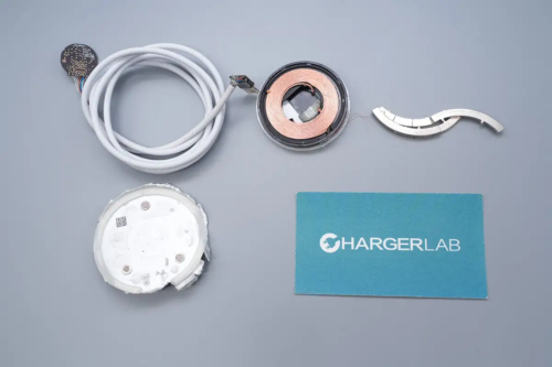
The PCBA module is removed from the housing.
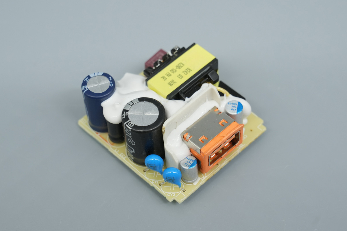
The front of the PCBA module is fully encapsulated with white potting compound between major components such as the transformer and caps, which provides structural stabilization and thermal management.
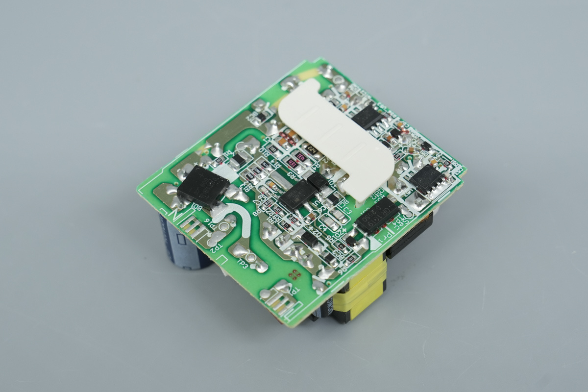
The back of the PCBA features a highly organized arrangement of SMD components, a hollow design exists between the primary and secondary stages, complemented by a white insulation isolation PCB.
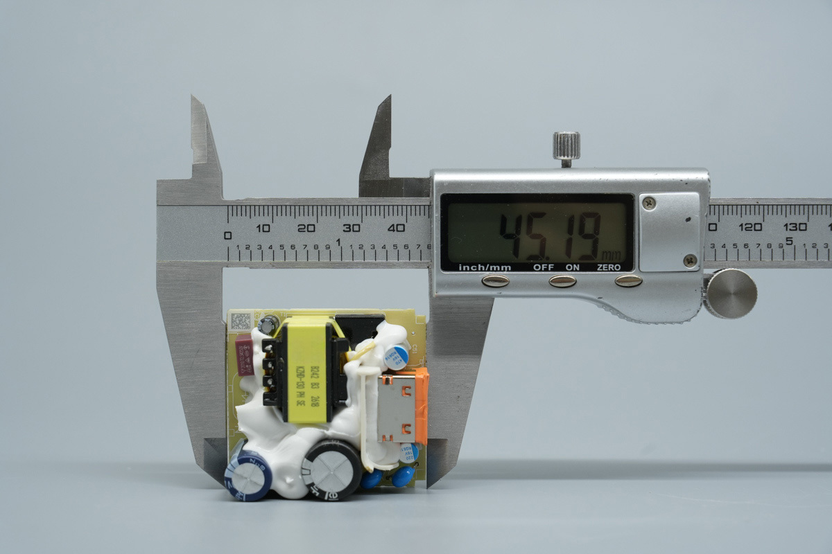
The length of the PCBA is about 45.19mm (1.779 inches).
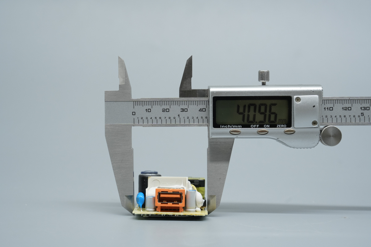
The width of the PCBA is about 40.96mm (1.613 inches).
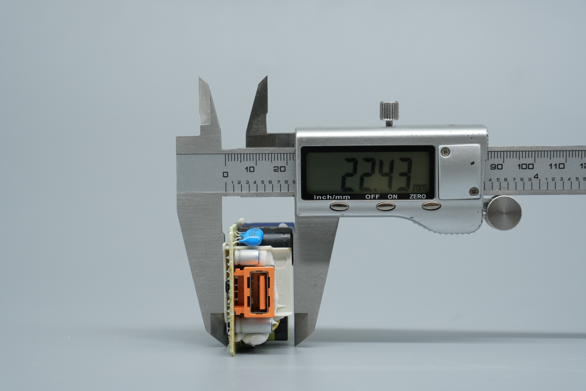
The thickness of the PCBA is about 22.43mm (0.883 inches).
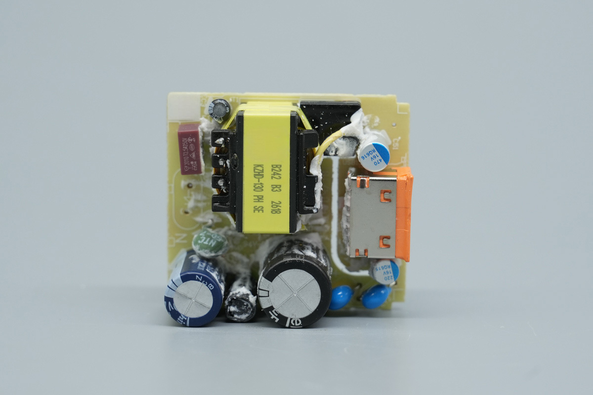
With the white potting compound cleared away, the front of the PCBA is shown to be composed of key sections including input filtering, a high-frequency transformer, and output filtering.
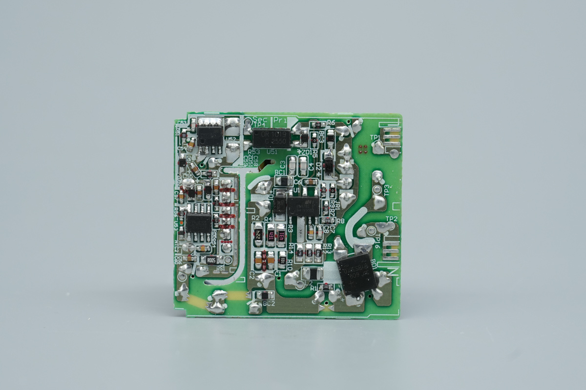
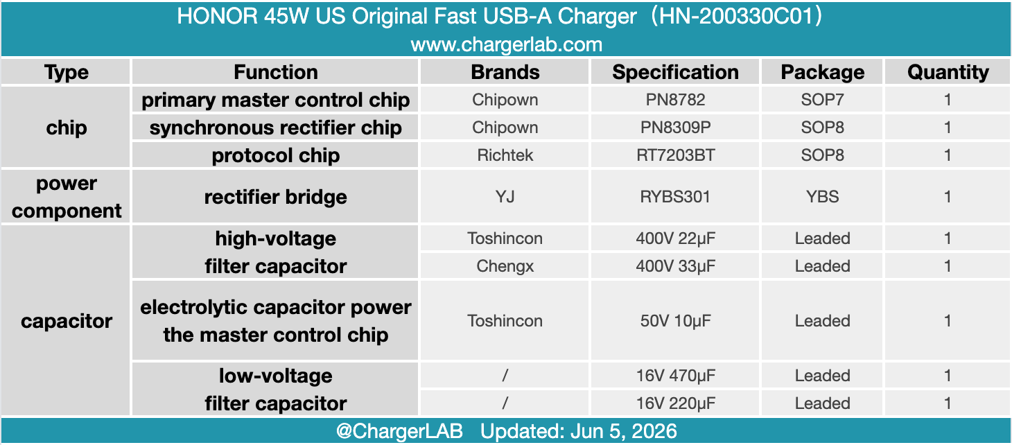
Removal of the white insulation PCB from the back of the PCBA, showing that the circuitry consists of the primary master control chip, synchronous rectifier chip, protocol chip, and related power components.
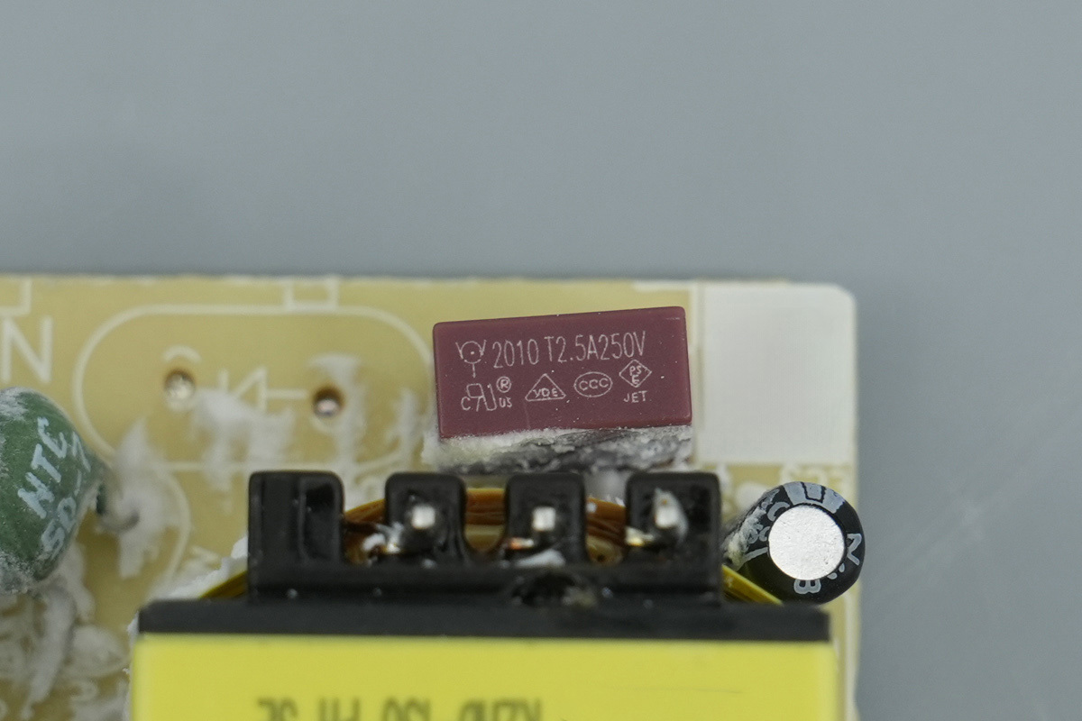
A time-delay fuse at the input end, 2.5A 250V, which provides protection against input overcurrent.
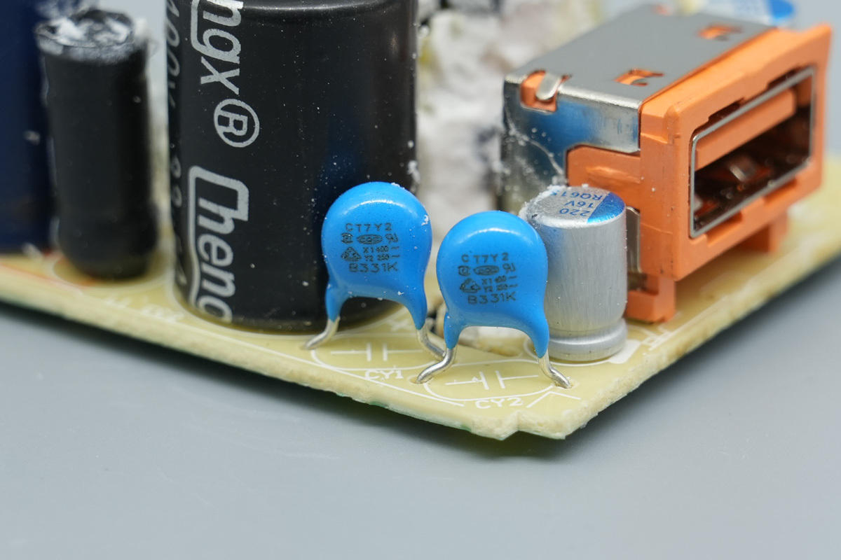
Two blue Y-caps, B331K.
Positioned between the two caps is an I-shaped choke, encased in black heat-shrink tubing, which functions as an input filter.
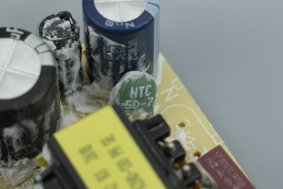
A green NTC thermistor, marked 5D-7, is utilized to suppress inrush current upon startup.
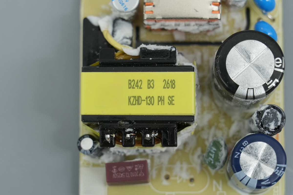
The transformer, marked B242 B3 2618 KZHD-130 PH SE.
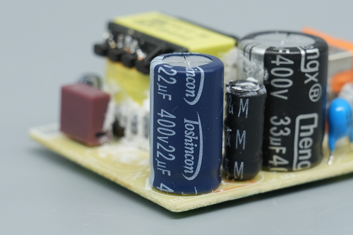
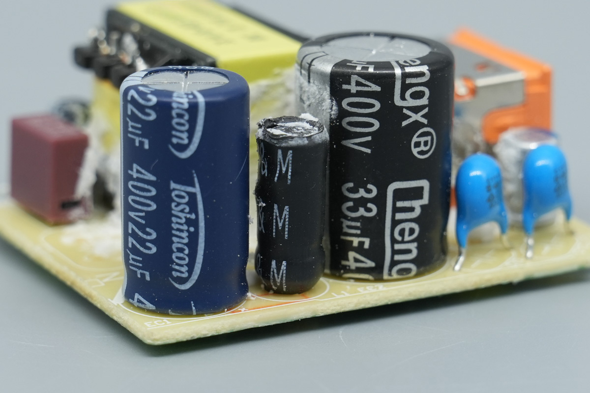
A high-voltage filter cap is from Toshincon, spec 400V 22μF.

Another one is from Chengx, spec 400V 33μF.
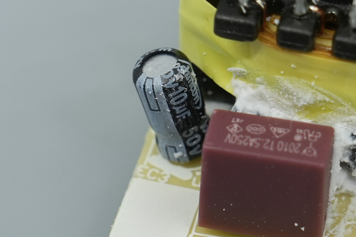
The electrolytic cap powering to the primary master control chip is also from Toshincon, spec 50V 10μF.
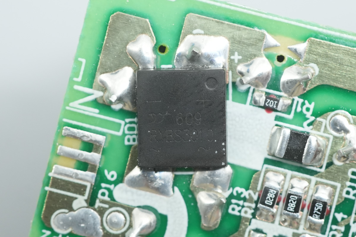
The rectifier bridge located on the back of the PCBA is from YJ, model RYBS3010, spec 1000V 3A and in a YBS package.
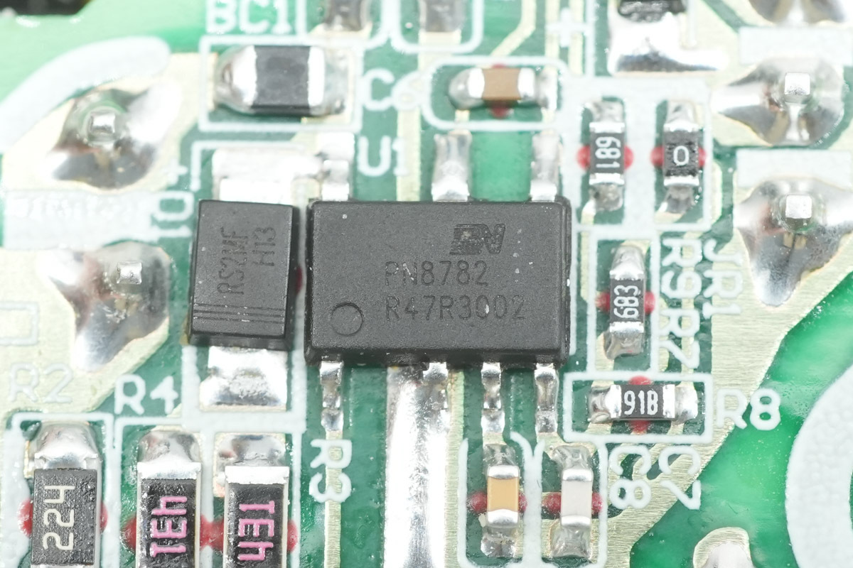
The primary master control chip is from Chipown, model PN8782, in an SOP7 package. This high-frequency quasi-resonant AC/DC converter is engineered specifically for high-performance fast-charging switch-mode power supplies.
Featuring a high level of integration, it incorporates a current-mode controller, a high-voltage startup circuit, and a high-performance high-voltage GaN FET, making it an ideal solution for mobile chargers and other modern smart device power applications.
The PN8782 features an adaptive operating mechanism that intelligently switches between QR-Lock, PFM, and Burst modes to suit varying voltage and load conditions.
By pairing this multi-mode modulation with QR-Lock technology, the design delivers high efficiency across the load range, minimizes noise, and ensures minimal standby power. Additionally, with an 8–57V supply range and integrated frequency modulation and Soft-Driver features, the system maintains excellent EMI characteristics.
An optocoupler, marked OR1019.
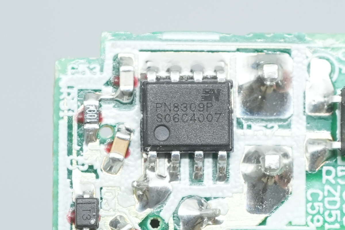
The synchronous rectifier chip is also from Chipown, model PN8309P, in an SOP8 package. This device is a synchronous rectification controller with an integrated power MOSFET that supports continuous conduction mode, specifically engineered to replace traditional secondary-side Schottky diodes in AC/DC flyback systems.
By integrating an internal NMOS, it enhances the system's current output capability and improves overall power conversion efficiency, enabling the design to easily meet Level VI energy efficiency standards.
The PN8309P is compatible with various operating modes, including CCM, DCM, and QR, and utilizes current-tracking turn-off technology. Additionally, the chip integrates comprehensive auxiliary functions, including input under-voltage protection and minimum on-time configuration.
Its unique high-voltage self-power supply technology supports a high-side, auxiliary-winding-free design, while dual-power supply technology further extends the output voltage range in low-side applications, thereby providing a highly reliable and integrated solution for modern fast-charging and high-efficiency power systems.
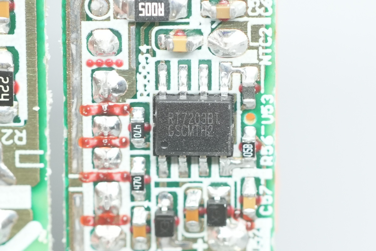
The fast-charging protocol chip is from Richtek, model RT7203BT, in an SOP8 package. This chip integrates an MCU, CV/CC control loops, feedback compensation circuitry, and a 10-bit ADC, enabling flexible support for various proprietary fast-charging protocols via the D+/D- interfaces.
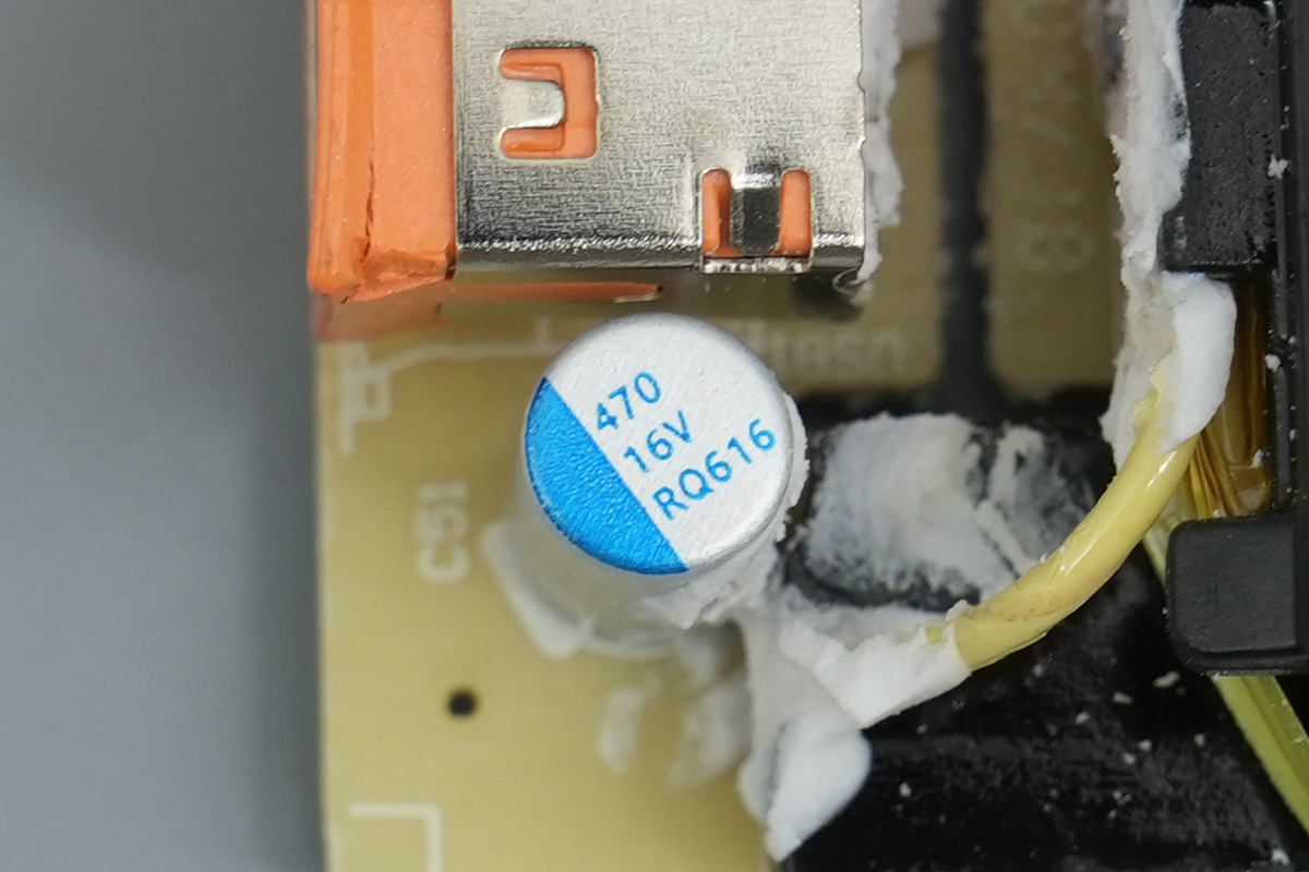
The output filtering cap, spec 16V 470μF.
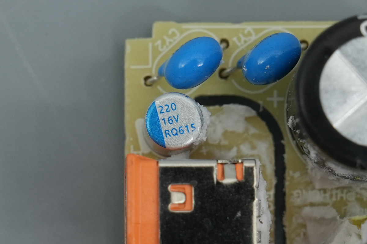
Another one is with a spec 16V 220μF.

Well, those are all components of the HONOR 45W US Original Fast USB-A Charger.
Summary of ChargerLAB
Honor’s 45W US-spec USB-A charger maintains the brand’s minimalist aesthetic, boasting a tactile white micro-matte shell and a compact, travel-friendly design. It excels in performance, supporting QC, FCP, and SCP protocols to provide up to 45W of SuperCharge power to Honor and Huawei devices.
The teardown highlights an impressively efficient single-sided PCB design. By integrating Chipown's PN8782 and PN8309P power solution with Richtek’s RT7203BT protocol chip, Honor has achieved a 45W output with minimal componentry. The result is a robust, durable, and highly reliable original charger.
Related Articles:
1. Teardown of HONOR 120W GaN Charger (HN-200600C02)
2. 10,000mAh Battery | Charging Compatibility Test of HONOR WIN
3. Porsche Design | Charging Compatibility Test of HONOR Magic7 RSR