Introduction
With the implementation of the new Chinese standard GB 47372—2026, mobile power safety has entered a new era. Anker, a key contributor to these standards, is at the forefront with its latest innovation: the Anker Nano 10000mAh ultra-thin magnetic power bank.
Designed to be both slim and powerful, this unit packs a 10000mAh capacity into a chassis just 14.76mm thick. It’s a game-changer for iPhone users, delivering nearly two full charges in a portable footprint.
Whether you’re traveling or multitasking, its sleek magnetic design attaches perfectly to the rear of your phone. It stays out of the way, avoiding any interference with the camera module or the phone's bottom edge, ultimately providing a premium, hassle-free charging experience that feels as good as it looks.
This power bank delivers 15W wireless charging alongside a powerful 30W bidirectional USB-C wired fast charge. With support for major protocols like PD3.0, FCP, SCP, and QC, it’s versatile enough to fuel everything from smartphones to tablets and ultrathin laptops.
Fully compliant with the new 2026 national safety standards, it is safe for air travel and offers a smart user experience: connect via cable to the official Anker App to track battery health, operating temperature, and charge cycles in real time.
We’ve torn it down to give you an inside look at the engineering and premium components that power this device.
Product Appearance
The front of the packaging box features Anker's classic white and blue color scheme, with the Anker brand logo and product name printed on it. It also indicates that it supports 15W Max wireless output and 30W Max wired output, highlighting its ultra-thin design.
The side of the box features a prominent ANKER Nano logo.
The box features a blue hanging tab at the top, along with a sticker displaying the product's SN barcode.
The bottom features a barcode and indicates that the outer packaging is printed using eco-friendly soy-based ink.
Usage scenarios, product highlights, and specs listed on the back of the box. And the detailed technical specs will be covered in the upcoming physical review.
The box includes the Anker magnetic power bank unit, a matching white data cable, a black storage pouch, and the product user manual.
Featuring a sleek, pure white matte finish with a skin-friendly feel, the front of the unit is clean and minimalist, centered with the iconic Anker logo.
With its softly rounded edges and corners, it embodies a thoroughly minimalist design.
The base of it features a silver metallic frame design, integrated with a single USB-C port and a set of LED indicators.
The indicator array consists of five apertures, with the rightmost indicator dedicated to displaying the charging status.
A silver, elongated power button is located on the side of the unit.
The surface of the power button features a refined concentric circular texture, enhancing tactile feedback for blind operation.
The top of the unit is clean and unobstructed, featuring no openings or ports.
The silver side frame features laser-engraved product info.
Device Specs (Side Plate):
Product: Anker Nano Magnetic Power Bank
Model: A1113
Rated Energy: 39.2Wh
USB-C Input: 5V3A, 9V3A, 15V2A (Max 30W)
USB-C Output: 5V3A, 9V3A, 12V2.5A, 15V2A, 20V1.5A (Max 30W)
Wireless Output: Max 15W
Total Output: USB-C 5V2.4A (Max 12W); Wireless: Max 12W
Manufacturer: Anker Innovations Co., Ltd.
Production Facility: Hunan Giantsun Power Electronic Co., Ltd.
Recommended Safe Service Life: 5 Years
Adjacent to these, there are safety certification marks such as the CCC logo and the environmental protection usage period indicator. The production date is marked as April 29, 2026.
The magnetic charging area on the back of it features a lightning bolt icon in the center, with an alignment magnet positioned below it.
The magnetic coil area is delineated by a detailed array of concentric ring markings.
This zone features bar-shaped alignment magnets, ensuring your smartphone remains securely and stably attached to the power bank.
This is the bottom USB-C port, featuring a dark blue plastic sheet. The adjacent "IN/OUT" marking indicates support for bidirectional charging.
Upon pressing the power button, two white LED indicators illuminate.
That's how big it is in the hand.
The length of the power bank is about 104.24mm (4.104 inches).
The width of the power bank is about 71.06mm (2.798 inches).
The thickness of the power bank is about 14.76.mm (0.581 inches).
The weight is about 217.2g (7.66 oz).
The included white USB-C to USB-C charging cable is secured with a rubber cable tie.
The connector head of the data cable is embossed with the Anker logo.
ChargerLAB POWER-Z KM003C shows that the cable supports that it doesn't contain an E-Marker chip.
The length of the data cable is approximately 62 cm (24.41 inches).
ChargerLAB POWER-Z KM003C shows that the USB-C port supports QC3+, FCP, SCP, AFC, PD3.0/PPS, QC4+, DCP, SAM 2A and Apple 2.4A.
And it also supports three fixed PDOs of 5V3A, 9V3A, 12V2.5A, 15V2A and 20V1.5A, and features PPS subset: 5.00-11.00V 2.75A.
When charging the iPhone 17 Pro, the power output can reach up to 28W.
When attached to the back of the iPhone, it sits flush against the rear panel without obstructing the camera module.
When attached, it does not extend beyond the bottom edge of the iPhone.
The magnetic connection is remarkably strong, allowing you to lift the power bank by the device alone without it detaching.
Once attached, the iPhone immediately displays the Qi2 wireless charging animation.
It also supports a wired connection to the official Anker app.
The app provides a clear, intuitive dashboard where you can easily view the power bank's remaining capacity, battery health, and cycle count.
After a thorough look at the design and fast-charging compatibility, ChargerLAB now takes you inside with our detailed product teardown.
Teardown
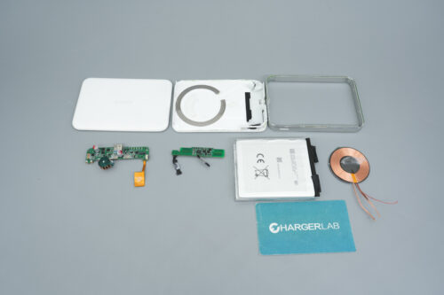
Prying along the seam of the chassis, the pure white front cover is removed to reveal the internal structure.
The inner side of the front cover is lined with a large black sticker and green barley paper for insulation.
Turning to the PCBA, we observe a substantial amount of gray thermal potting compound applied around the mainboard and the connector interfaces.
机身内部全貌大部分空间被锂聚合物电芯占据。
The majority of the internal space is occupied by the lithium-polymer battery cell.
On one side of the battery cell, an NTC thermistor probe is installed to monitor temperature, secured in place with yellow high-temperature tape.
We then proceed to fully extract the battery cell and PCBA assembly from the rear casing.
The back cover features a ring-shaped magnetic array for MagSafe, accompanied by positioning magnets below, while the right side accommodates cutouts for the interface and power LED indicator.
The back of the battery cell is covered with a large area of cyan insulating tape, and the wireless charging coil assembly and the magnetic attachment detection ribbon cable are placed in the center.
The PCBA features a green solder mask design. Solder joints for the magnetic attachment detection ribbon cable, the NTC thermistor, and the wireless charging coil are all reinforced with potting compound.
Here is the wireless charging coil and the black magnetic shielding sheet at the base; the coil is tightly wound using Litz wire.
A NTC thermistor is positioned at the center of the coil to monitor core temperature in real-time during wireless charging, preventing overheating.
The two battery cells are collectively soldered onto a single BMS PCB.
The corresponding NTC thermistor probe.
The two extracted ATL cells are connected in series.
The battery cells are from ATL, model 506578. Each cell has a capacity of 5,000 mAh, a nominal voltage of 3.92 V, and an energy rating of 19.6 Wh.
The lithium battery protection IC on the BMS PCB is from SOUTHCHIP, model number SC58540, housed in a QFN32 package.
Featuring a highly integrated architecture, the chip embeds drivers for high-side NMOS, pre-charge PMOS, and fuse control. It also integrates dual 16-bit high-precision ADCs, enabling accurate acquisition of battery pack total voltage, individual cell voltages, charge/discharge currents, and up to five temperature nodes, as well as Coulomb counting.
The SC58540 effectively reduces system BOM and simplifies PCB design, making it an ideal BMS solution for terminals such as laptops, drones, power tools, and portable energy storage systems.
Next to the chip are two lithium battery protection MOSFETs from LEADTECK, model LT7401FL, PMOS, -30V and 5.3mΩ, and in PDFN3*3 packages.
Here is the info about the LEADTECK LT7401FL.
Another lithium battery protection MOSFET is also from LEADTECK, model LT2002DNB, 20V and 3.8mΩ, housed in a TDFN2×3 package.
Here is the info about the LEADTECK LT2002DNB.
Turning to the PCBA, we can observe components distributed on one side, including the power bank SoC, wireless charging transmitter chip, and authentication chip.
The opposite side of the PCBA features the caps, the USB-C interface, resonant cap switching MOSFETs for wireless charging, the buck-boost chokes, buck-boost switching MOSFETs, and USB pass-through chip.
The power bank SoC is from IPower, model SW6303. This chip provides extensive support for fast-charging protocols, including the UFCS, as well as mainstream standards such as PD, SCP, FCP, AFC, QC, and SFCP, ensuring superior compatibility and charging efficiency.
The chip features an I2C interface, allowing for easy configuration of charging target voltage and current. It supports both 3–5 LED power indicators and a "188" digital tube display, providing users with intuitive performance and status monitoring. The SW6303 is housed in a QFN6×6-52 package, ensuring ease of integration and application.
Two buck-boost MOSFETs are from LEADTECK, model LTS3818FRDY, 30V and 3.5mΩ, housed in a TDFN3×3 package.
Here is the info about the LEADTECK LTS3818FRDY.
Other two buck-boost MOSFETs and the VBUS MOSFETs are also from LEADTECK, model LT3810FPJ, 30V and 11mΩ, housed in a TDFN3×3 package.
Here is the info about the LEADTECK LT3810FPJ.
The toroidal choke used for the buck-boost conversion.
A MCU from CHIPSEA, marked L011F8, is utilized to implement intelligent interaction functions.
A USB pass-through chip, model CH9347, from WCH, is used for data communication with the mobile app. Next to it are five LED indicators.
The wireless charging IC on the front of the PCBA is from CPS, model WB8118. The WB8118 is a high-efficiency magnetic induction wireless power transmitter IC that supports 15W Qi2 fast charging. It features a wide input voltage range of 3.3V to 18V, compatibility with wireless power receiver (ASK) communication, fixed communication interface ports, and a robust protection scheme against overvoltage, overcurrent, and overtemperature.
It integrates a voltage regulator, a full-bridge driver, an ASK demodulator, an FSK modulator, foreign object detection (FOD), a PWM module, and a multi-channel 12-bit ADC.
The authentication chip is from CPS, model CPS1010, a wireless charging protocol encryption IC specifically designed for Qi certification applications.
The chip integrates a SHA-256 cryptographic engine, ECC signature capability, and a true random number generator for key generation, providing identity authentication and secure certification support for wireless charging devices. It is housed in a DFN8 package.
A crystal oscillator is employed to provide the clock signal.
The filtering cap, 25V 100μF.
Another one shares the same model.
The resonant cap switching MOSFETs for wireless charging is from LEADTECK, model LTS1582FPC, 60V and 11mΩ, housed in a PDFN3.3×3.3 package.
Here is the info about the LEADTECK LTS1582FPC.
A chip, marked 6S2TI, and a device, marked 8ALPE.
Two chips, marked 1U1 Y28.
A ribbon cable used for monitoring the wireless charging status.
Well, those are all components of Anker Nano 10000mAh Ultra-Thin Magnetic Power Bank.
Summary of ChargerLAB
Our teardown reveals that the Anker Nano 10,000mAh magnetic power bank continues the brand's minimalist aesthetic, blending a skin-friendly white matte finish with a sleek silver metallic frame. Its magnetic grip is exceptionally strong, holding firm to an iPhone even when lifted single-handedly. Through the companion app, users can monitor charging status for a truly intelligent experience.
Under the hood, Anker delivers top-tier quality: it features an ATL battery cell managed by a SOUTHCHIP SC58540 protection IC, a iSmartWare SW6303 SoC, and a CPS WB8118 wireless transmitter paired with a CPS1010 authentication chip. Data connectivity for the app is handled by a CHIPSEA MCU and WCH’s CH9347, while power delivery relies on high-quality LAEDTECK MOSFETs.
Safety is paramount. The internal PCB is reinforced with extensive thermal potting compound, and multiple NTC thermistors monitor the battery and wireless coils to prevent overheating. In summary, this is a premium, well-engineered magnetic power bank that offers excellent build quality and reliability for any iPhone user.t build quality and reliability for any iPhone user.
Related Articles:
1. New York Times Square Goes Dark, Anker’s SOLIX S2000 Takes the Spotlight
2. Teardown of the Anker737 MagGo 3-in-1 Wireless Charger
3. Anker Launches Prime 14-in-1 Thunderbolt 5 Docking Station