Introduction
We obtained a 45W charger from MIIIW. This product is designed based on a complete integrated GaN power solution from Injoinic. True to its “Mini Magic Cube” name, the charger features a highly compact form factor and can be considered a mini-class product within the 45W power segment. Below, we take a closer look at the detailed design of the product.
Product Appearance
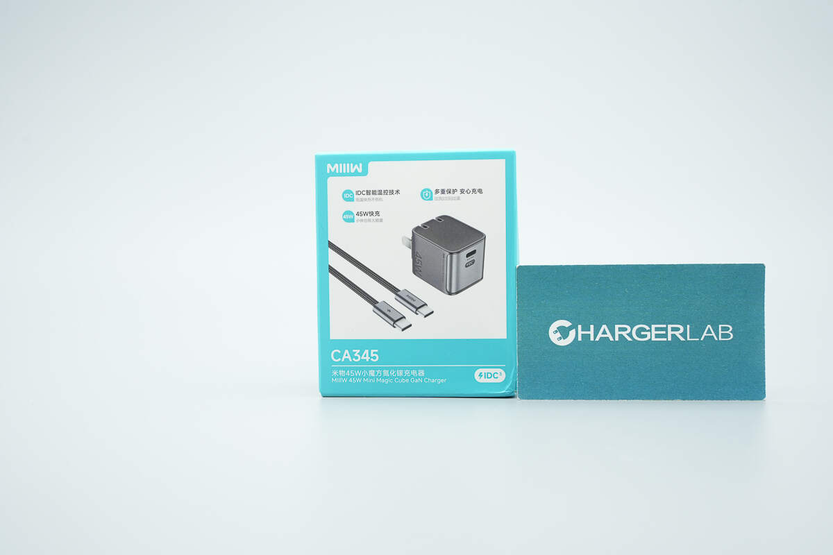
The front of the packaging box features the MIIIW branding, the product's appearance, the product name, and key selling points.
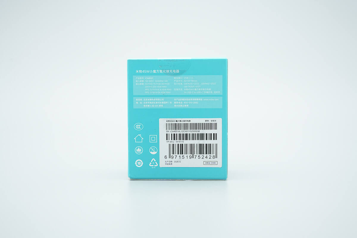
The back of the packaging box displays the technical specifications, manufacturer information, and other relevant details.
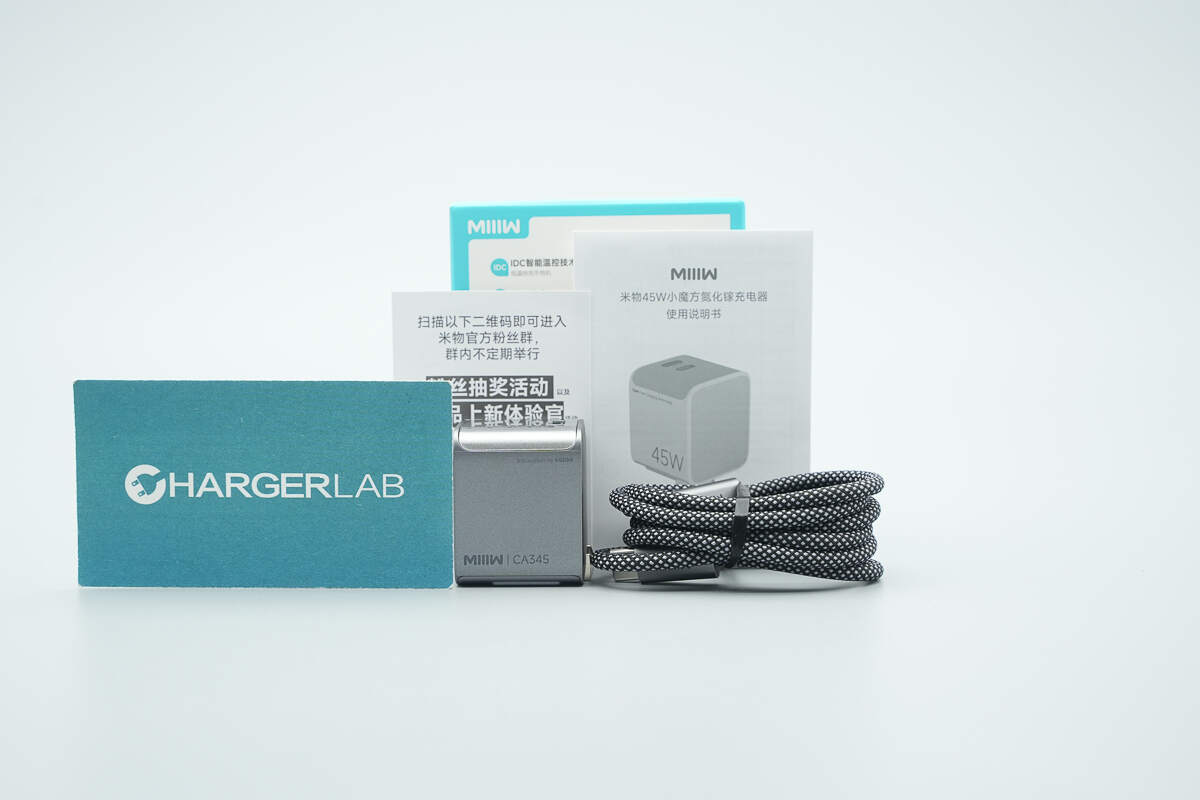
The package includes the charger, a data cable, a user manual, and other standard accessories.
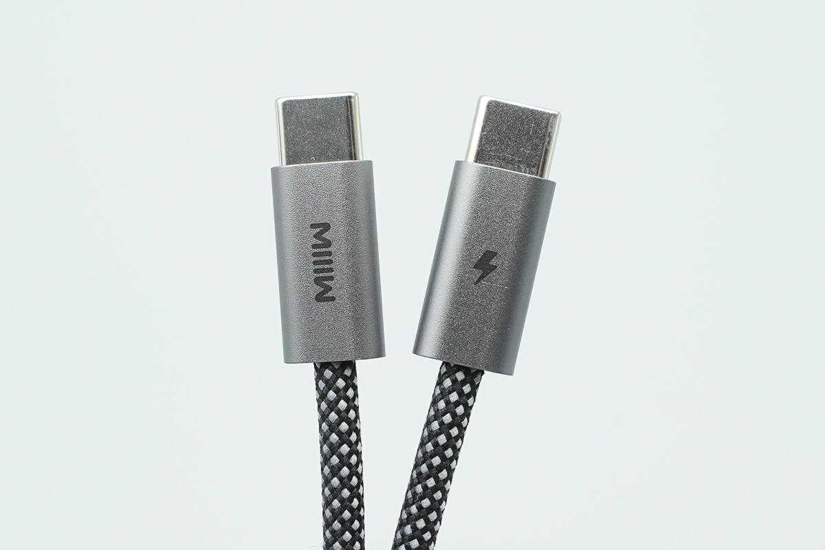
The included USB-C cable is a braided type, with connectors featuring metal housings.
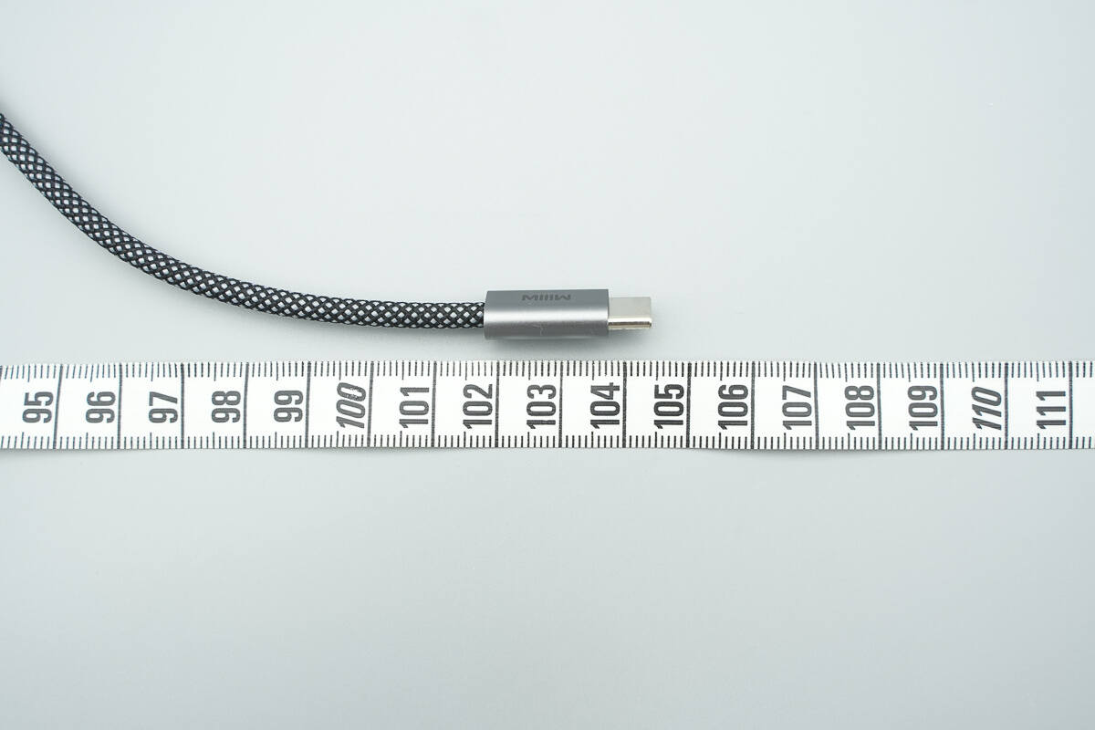
The length of the cable is about 104 cm (40.94 inches).
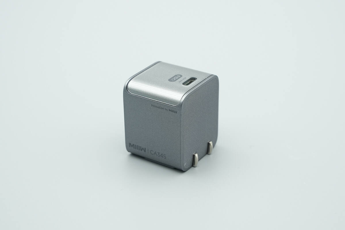
The enclosure features a gray finish paired with a silver decorative top panel, resulting in a compact and refined appearance.
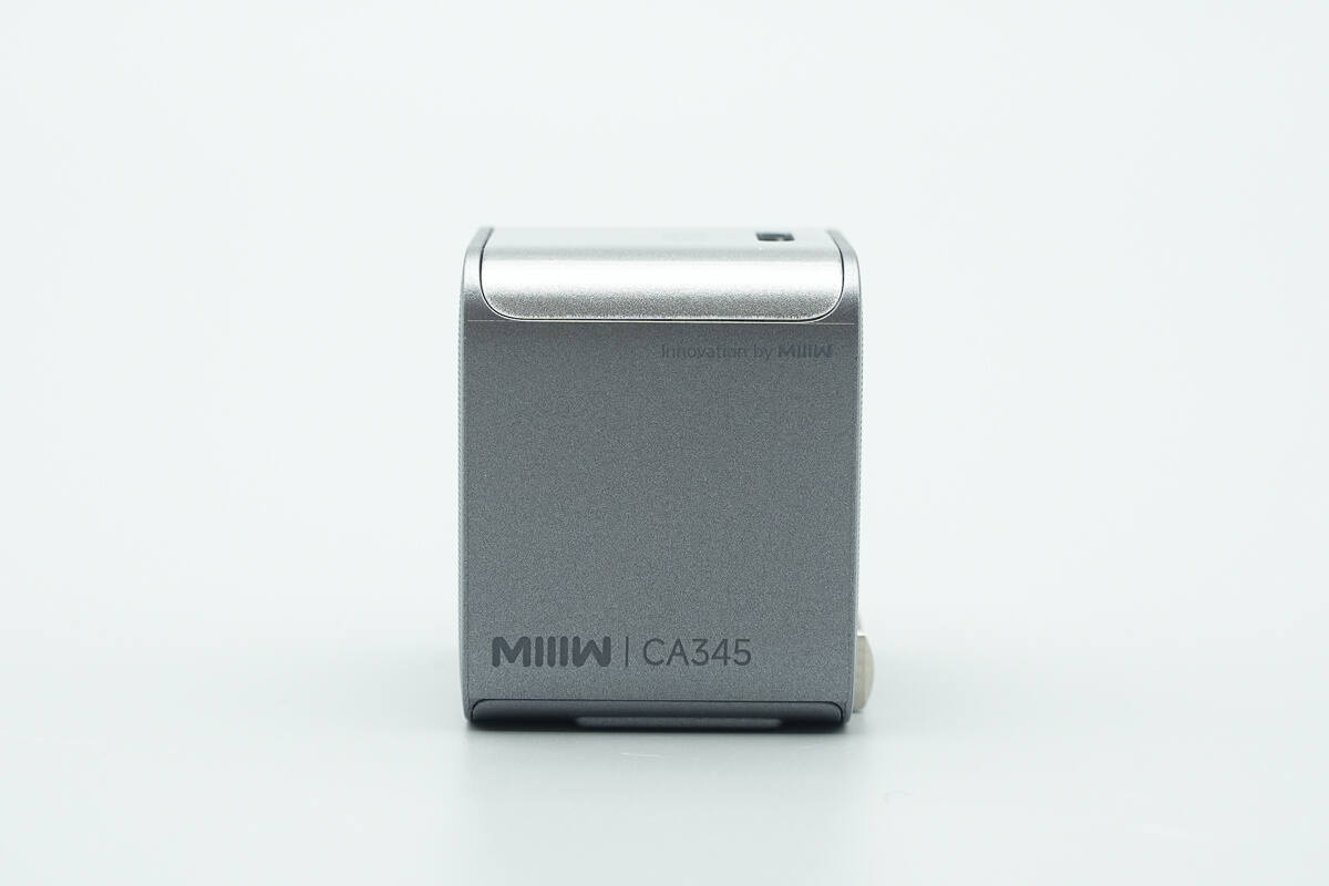
The front of the charger body is printed with the MIIIW branding and the CA345 marking.
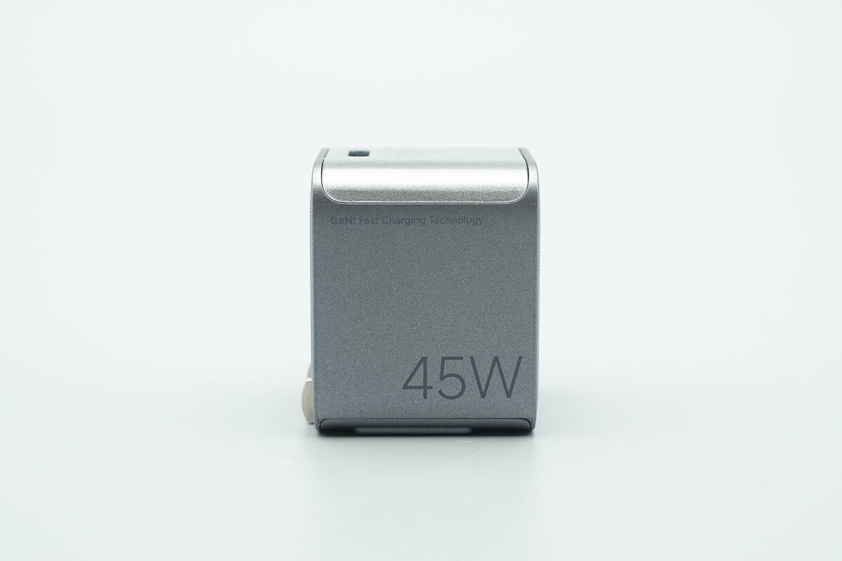
The opposite side is marked with “45W” and “GaN”.
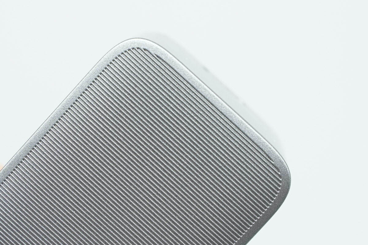
Both side panels adopt a textured design with raised and recessed patterns.
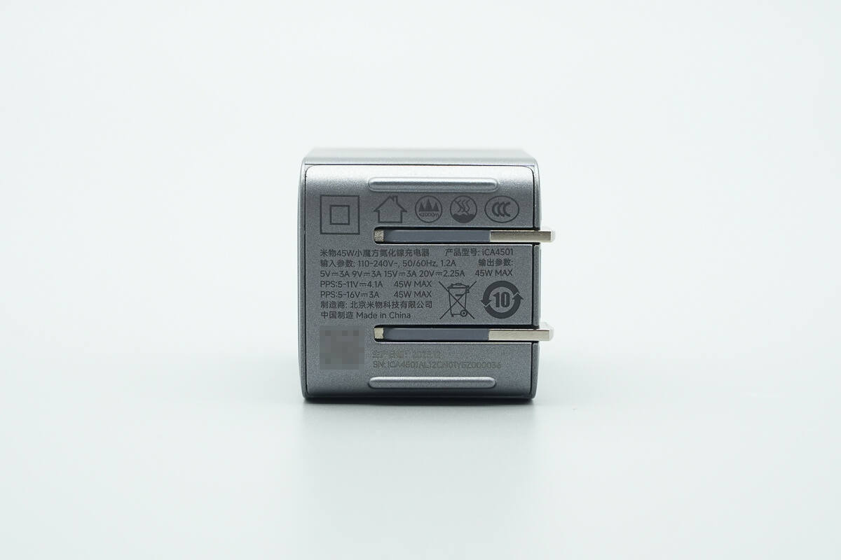
The bottom of the enclosure is printed with the technical specifications.
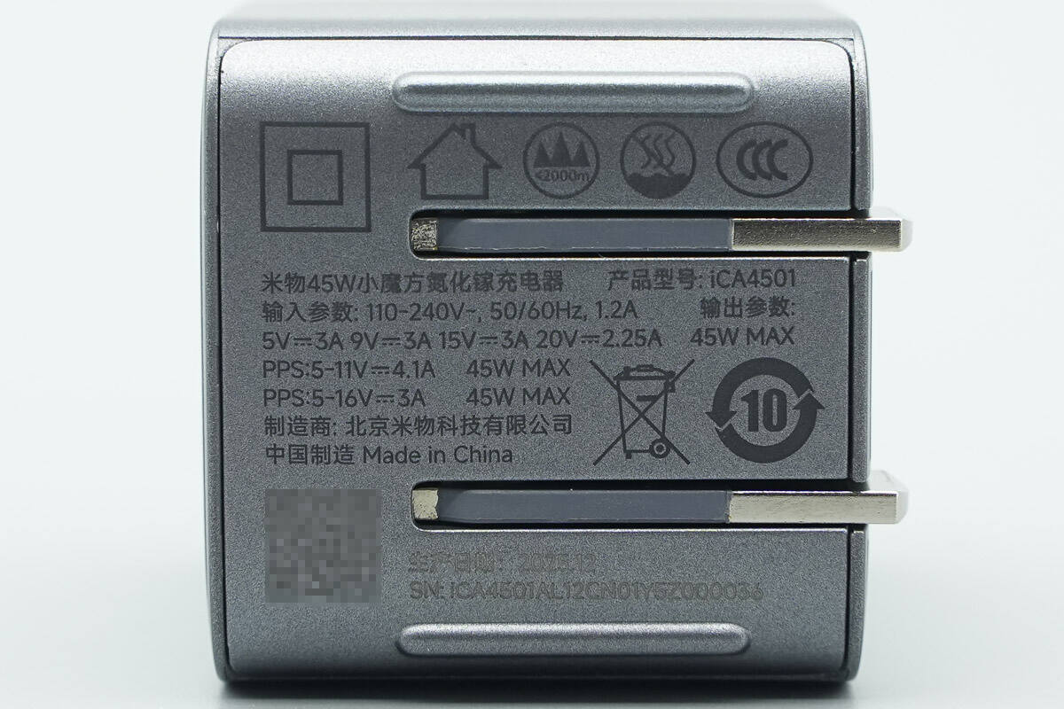
Product model: iCA4501
Input: 110–240V~50/60Hz 1.2A
Output: 5V 3A, 9V 3A, 15V 3A, 20V 2.25A, 45W MAX
PPS: 5–11V 4.1A, 45W MAX
PPS: 5–16V 3A, 45W MAX
The charger has passed CCC certification.
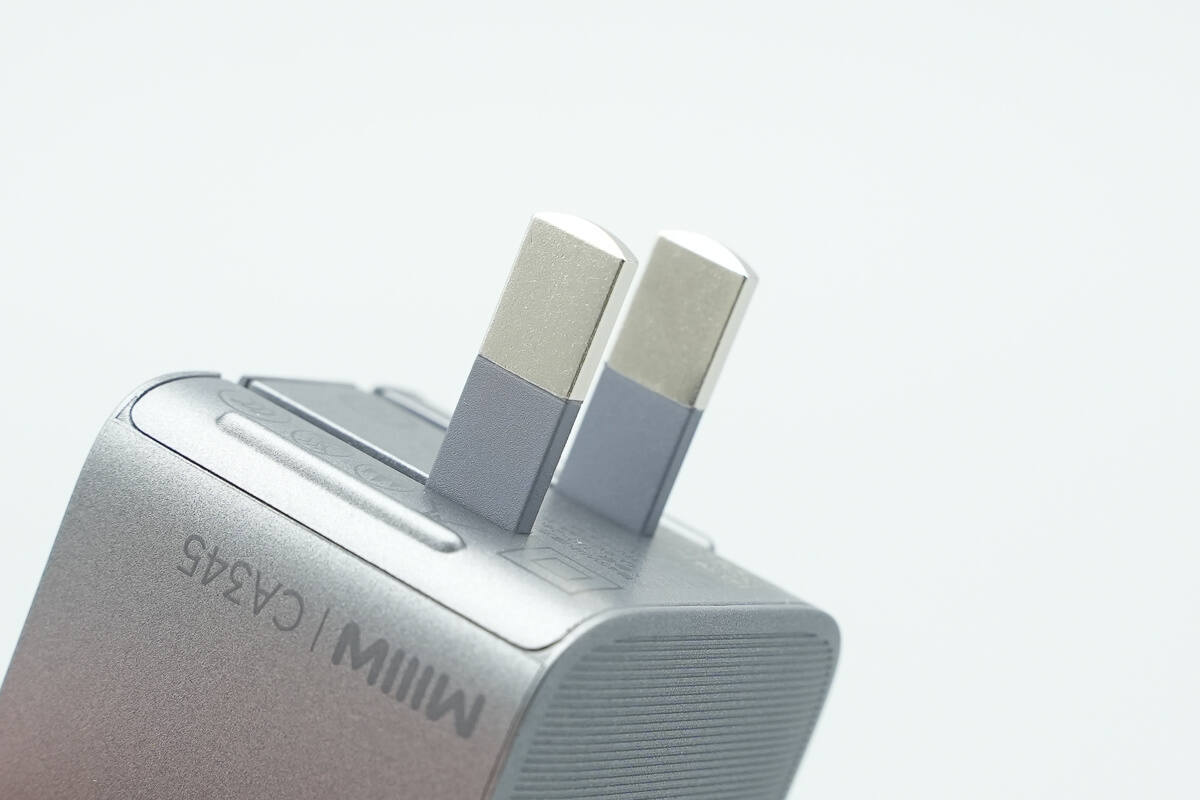
It is equipped with foldable prongs.
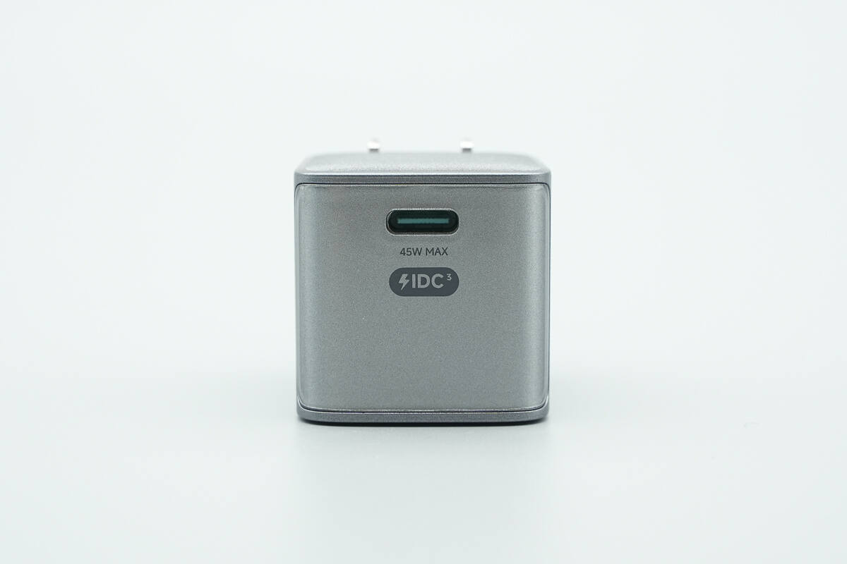
The top features a USB-C port, with the output power specifications printed next to it.
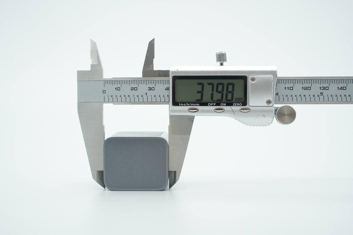
The length of the charger is about 37.98 mm (1.5 inches).
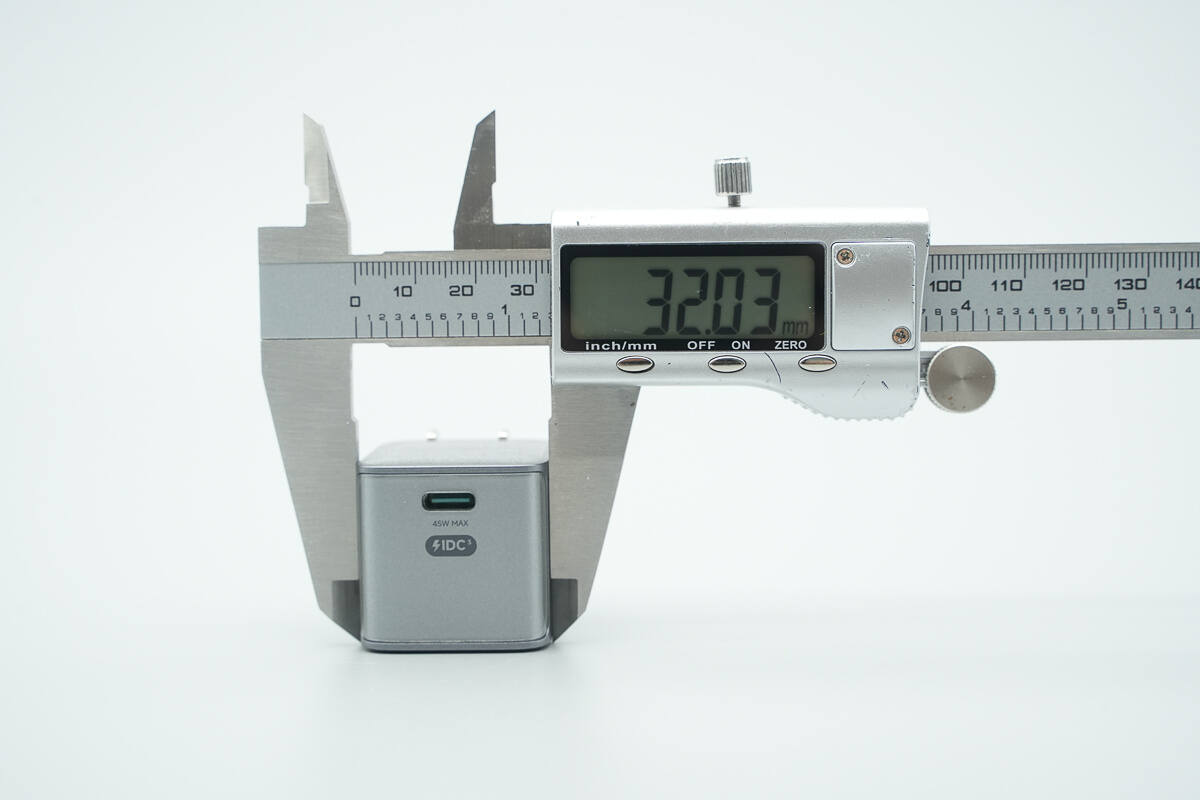
The width is about 32.03 mm (1.26 inches).
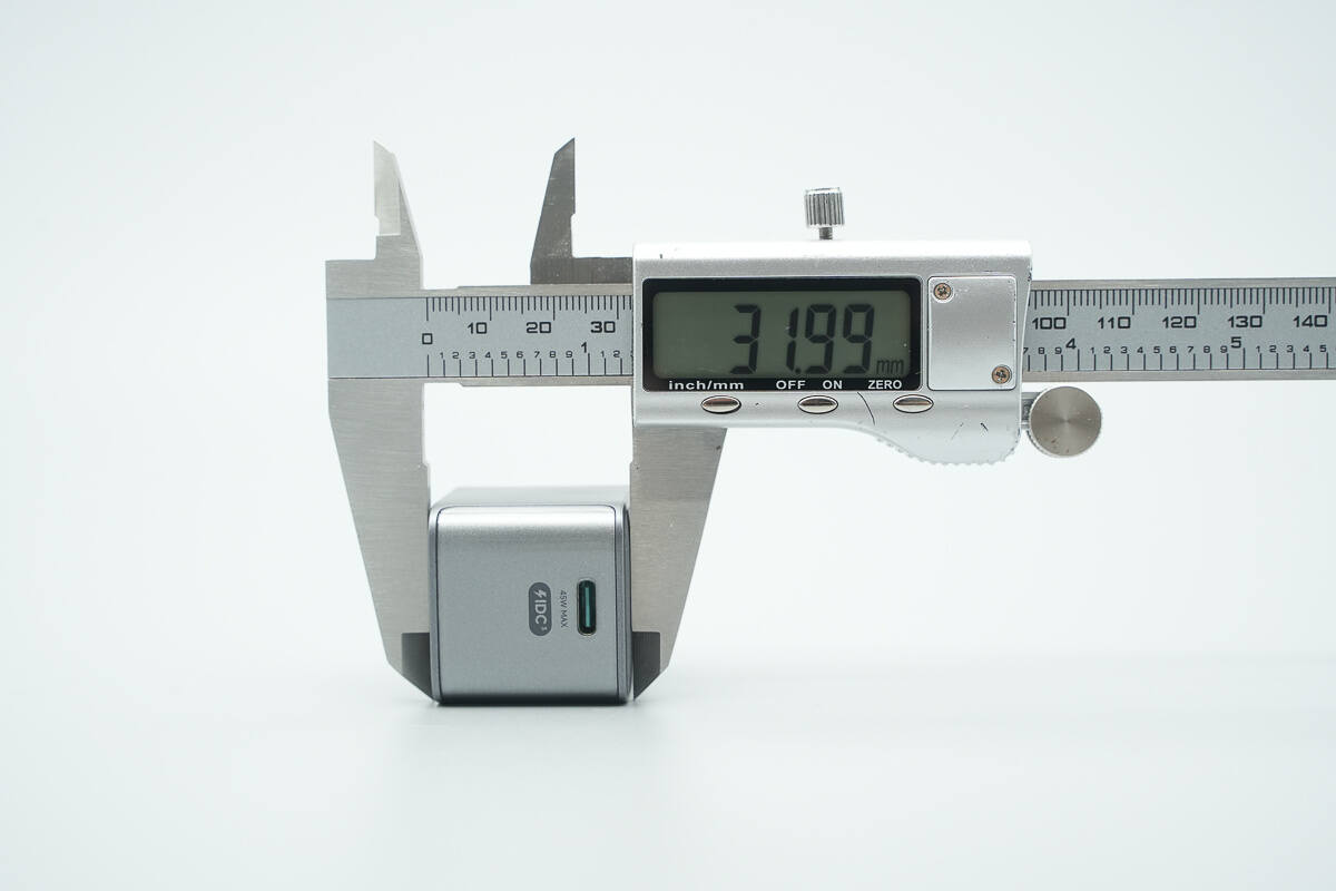
The thickness is about 31.99 mm (1.26 inches).

Its size is slightly smaller than that of the Apple 40W charger.
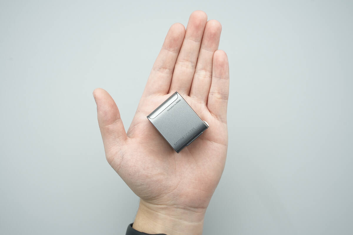
That's how big it is on the hand.
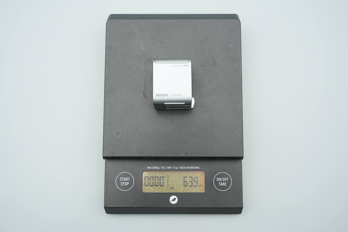
The weight is about 64 g (2.26 oz).
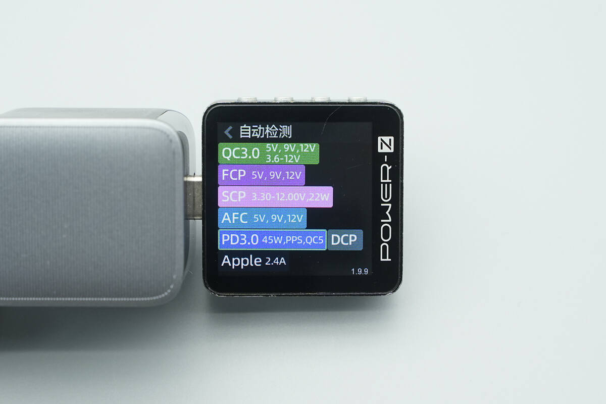
ChargerLAB POWER-Z KM003C shows that the USB-C port supports QC3.0/5, FCP, SCP, AFC, PD3.0, PPS, DCP, and Apple 2.4A charging protocols.

It features four fixed PDOs of 5V3A, 9V3A, 15V3A, and 20V2.25A. It also supports two PPS voltage ranges: 5–11V 4.1A and 5–16V 3A. Additionally, it is compatible with Xiaomi’s 48W Surge fast charging.
Teardown
Next, let's take it apart to see its internal components and structure.
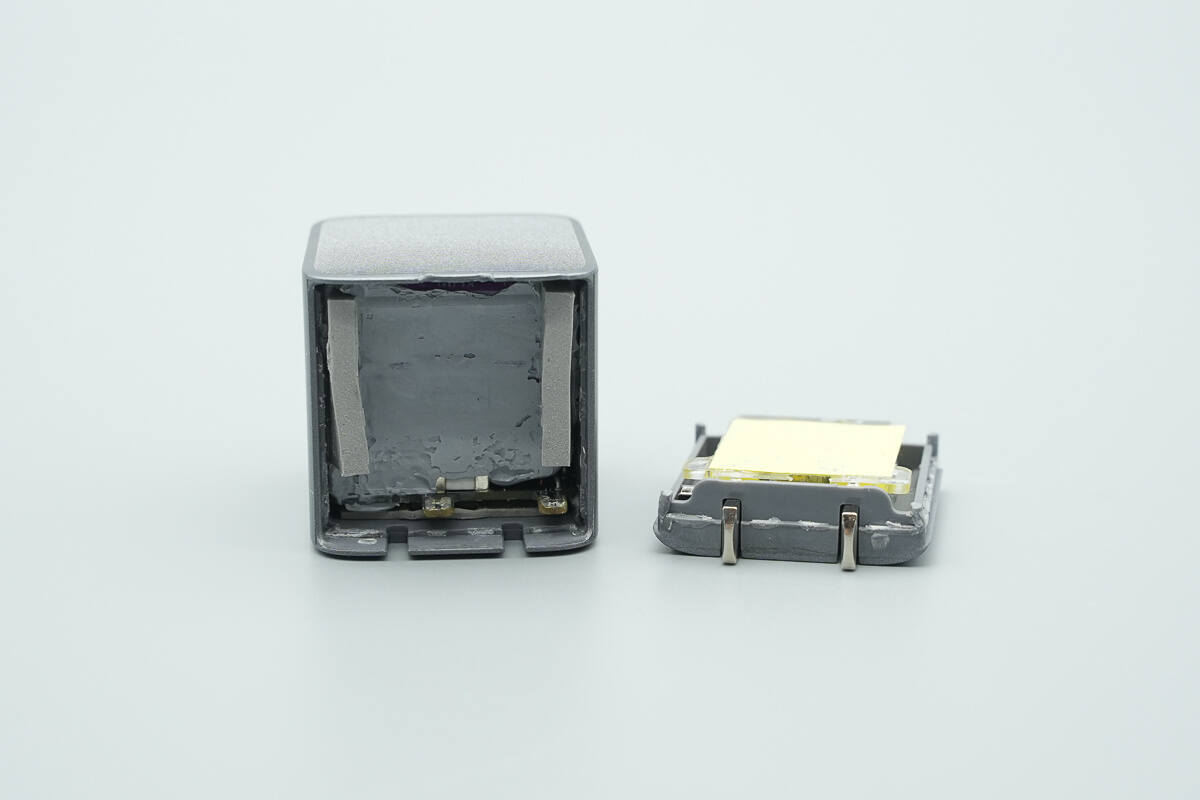
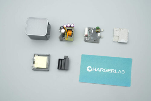
Opening the input-end enclosure reveals that it is sealed using ultrasonic welding.
The prongs are secured with a plastic cover and screws and insulated with tape.

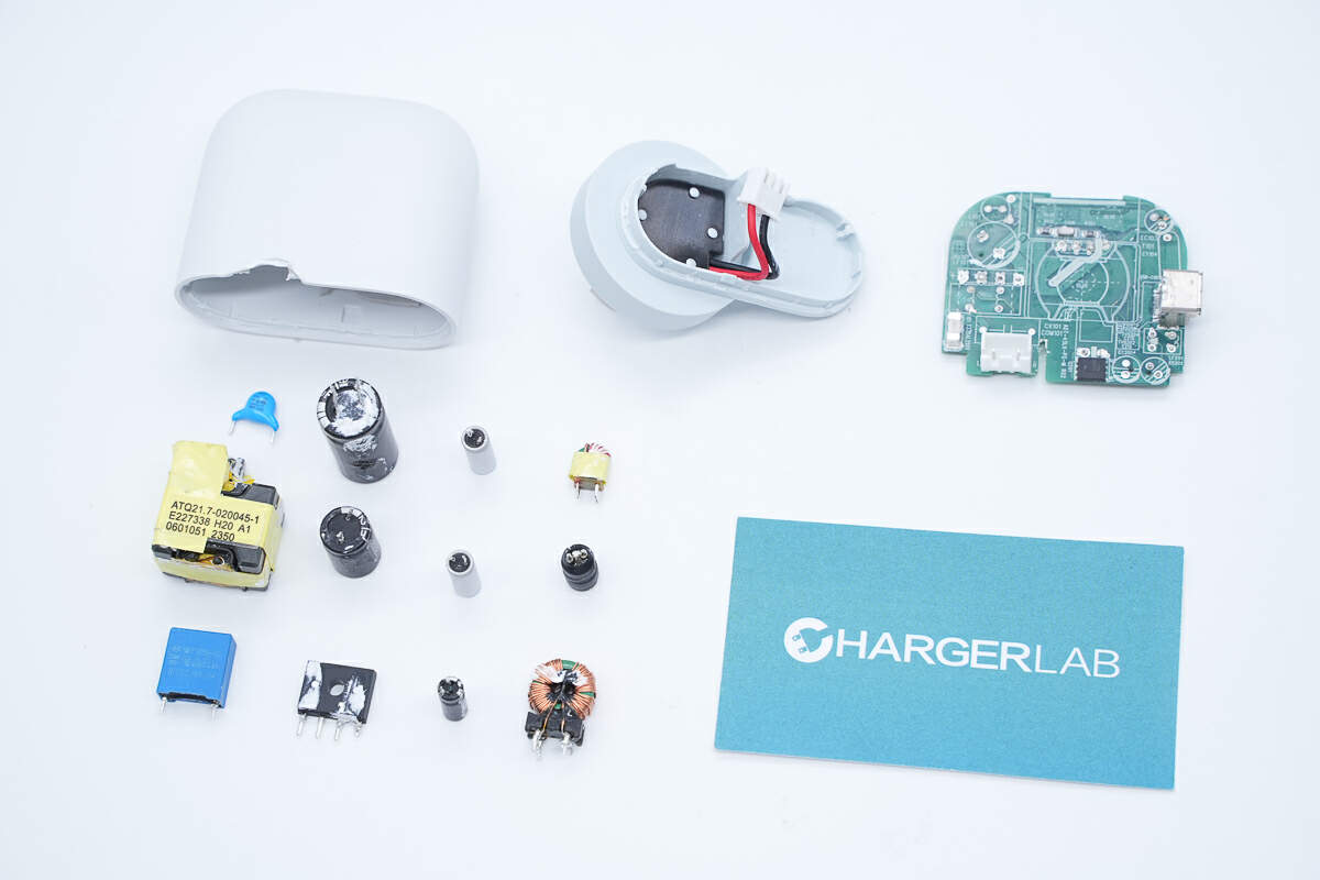
Remove the PCBA module.

The length of the PCBA module is about 33.13 mm (1.3 inches).
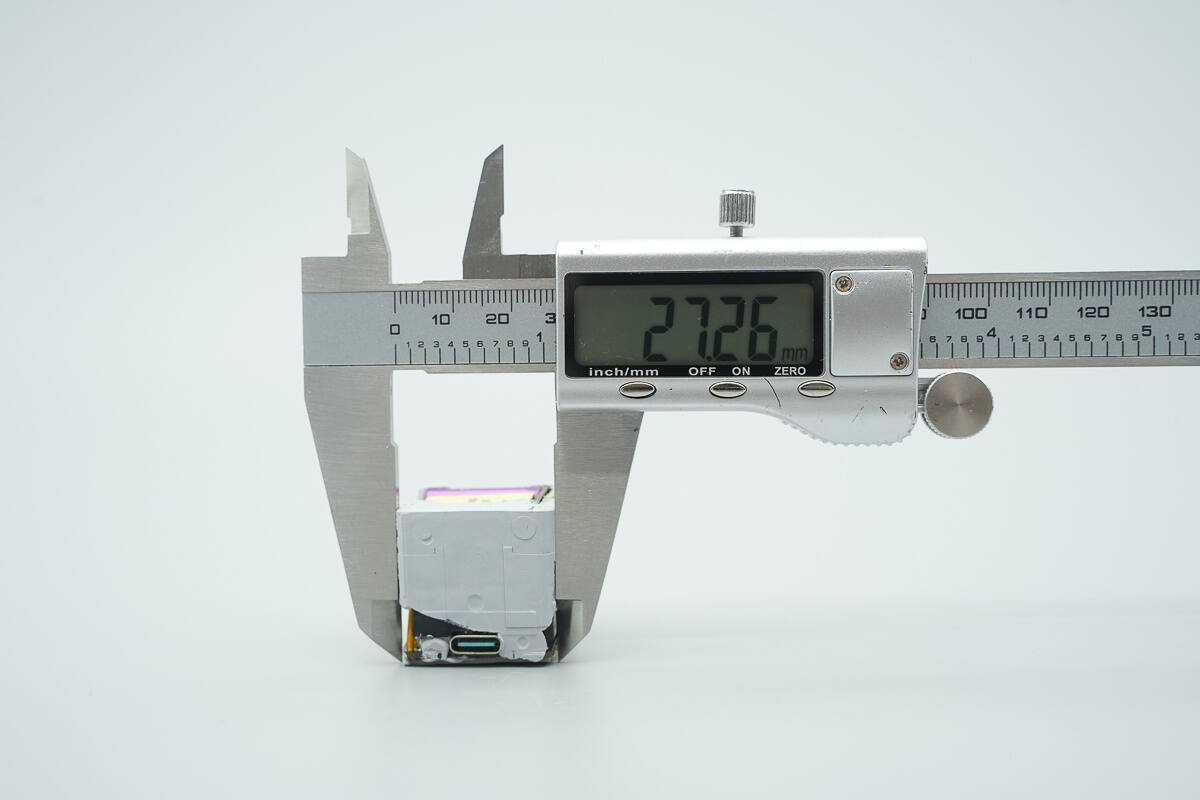
The width is about 27.26 mm (1.073 inches).
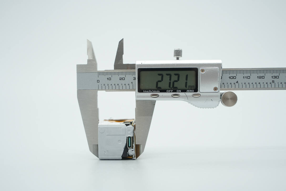
The thickness is about 27.21 mm (1.071 inches).
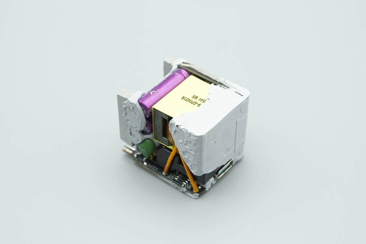
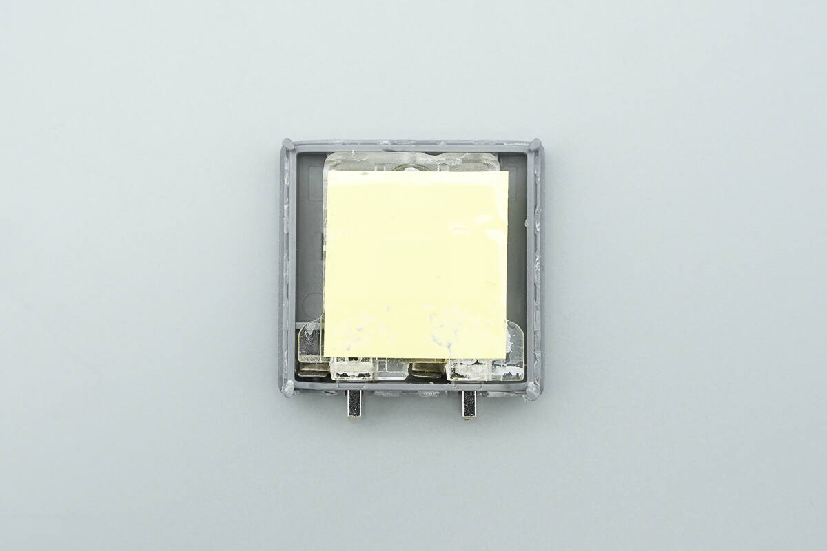
Thermal adhesive is applied to both the front and back of the PCBA module.

A thermal pad is also attached to the small side PCB.
The bottom of the module is also covered with a thermal pad.
Remove the thermal adhesive and pads. The PCBA module consists of two stacked PCBs, with a plastic casing providing isolation and insulation between the transformer and the capacitors.
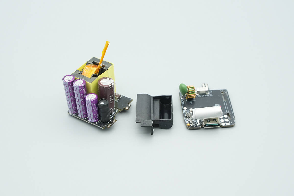
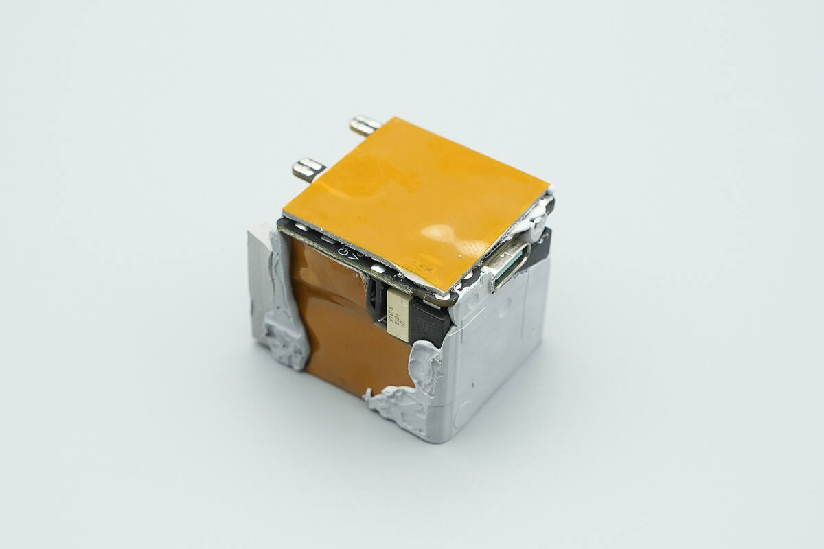
Disassemble the module into individual sections.

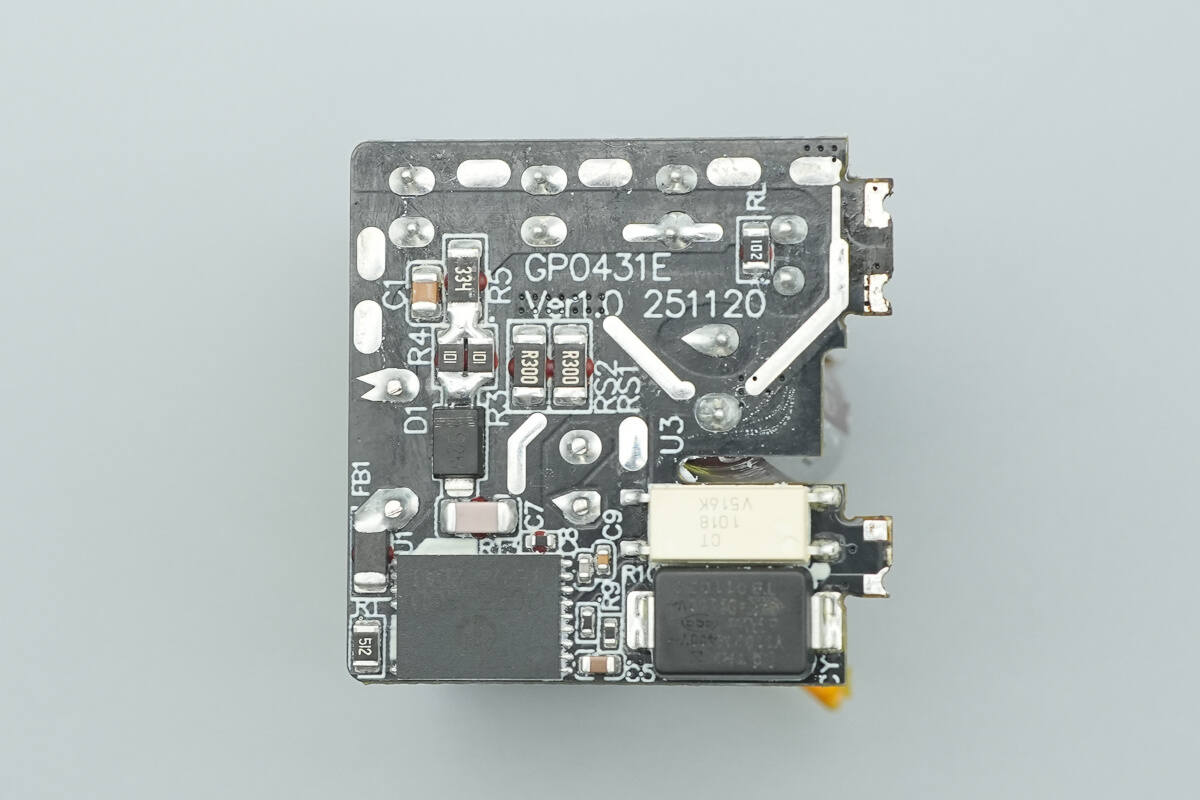
On the front of the bottom PCB, there are an SMD fuse, a common mode choke, an NTC thermistor, a synchronous rectifier controller, a filtering solid capacitor, and a VBUS MOSFET.
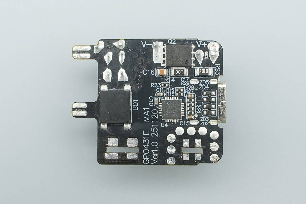
On the back, there is a bridge rectifier, a synchronous rectifier, and a protocol chip.
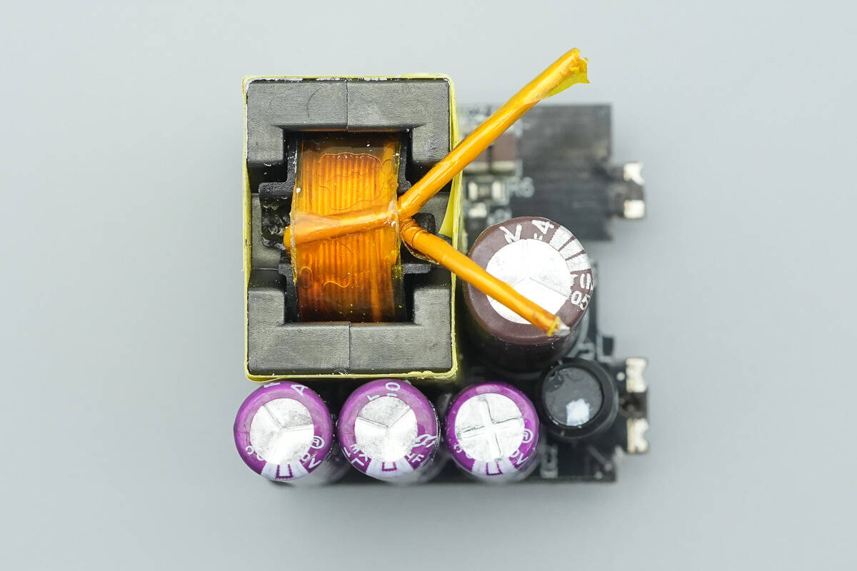
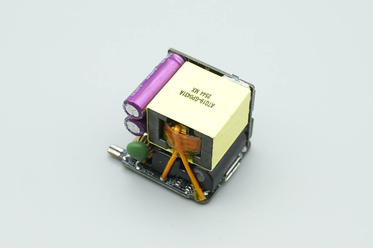
On the front of the side PCB, there is an I-shaped inductor, high-voltage filter electrolytic capacitors, and a transformer.
On the back, there is a master control chip, an optocoupler, and an SMD Y capacitor.

The SMD fuse is from Lanbao, rated at 3.15A.
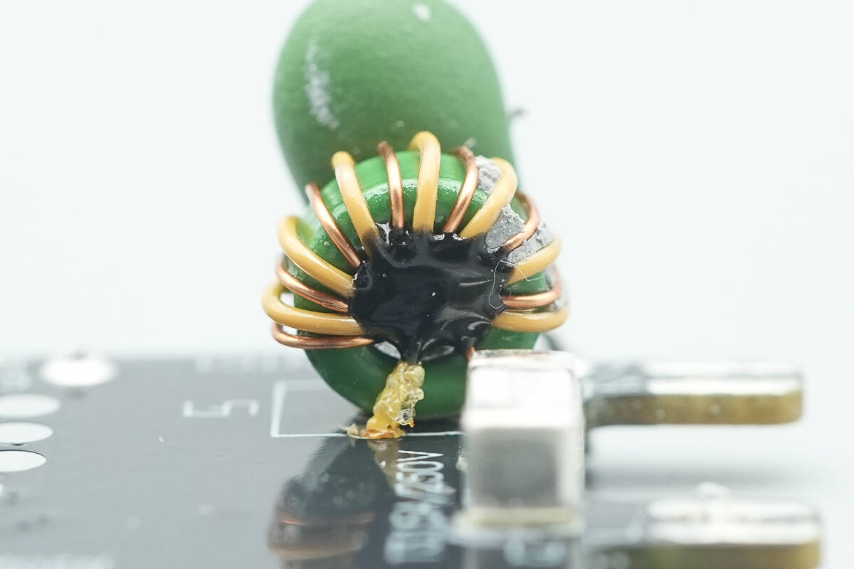
The common mode choke is dual-wound and used to suppress EMI.
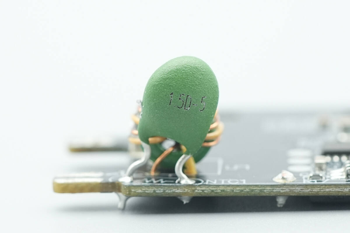
The NTC thermistor is used to suppress inrush current at power-on.
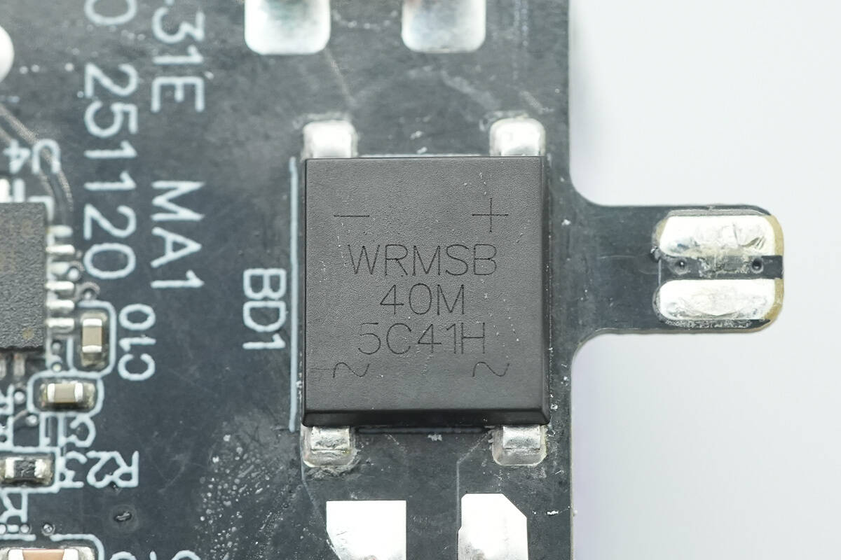
The bridge rectifier is from World Industrial, model WRMSB40M, rated at 4A 1000V. Its soft recovery curve and relatively smooth turn-off characteristics help minimize diode junction capacitance, effectively reducing harmonic oscillations.
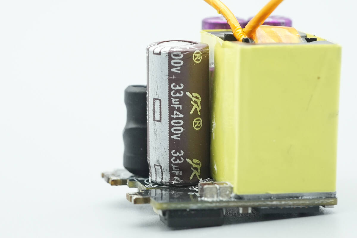
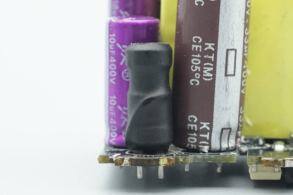
The high-voltage filter electrolytic capacitor is from JK, rated at 400V 33μF.
The I-shaped inductor is insulated with a heat-shrink sleeve.
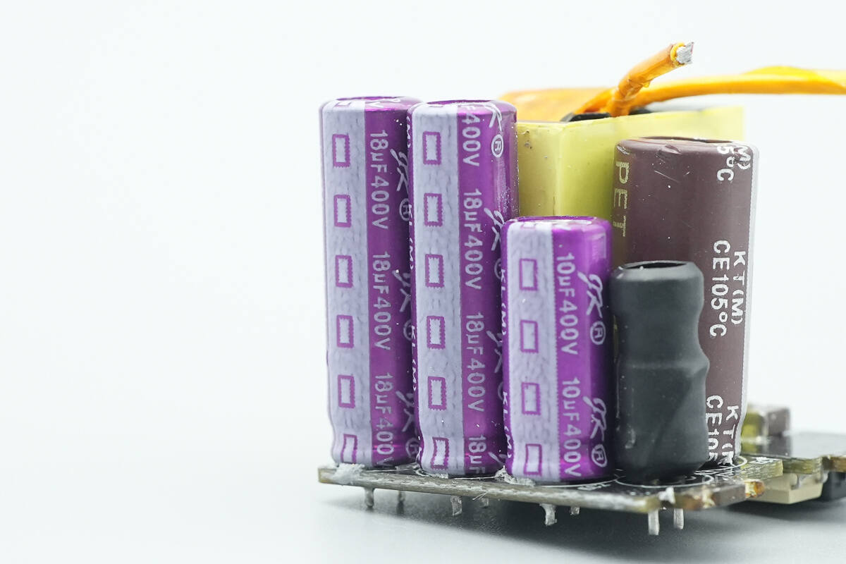
The other three high-voltage filter electrolytic capacitors are also from JK, with two of them rated at 400V 18μF.

The remaining capacitor is rated at 400V 10μF.
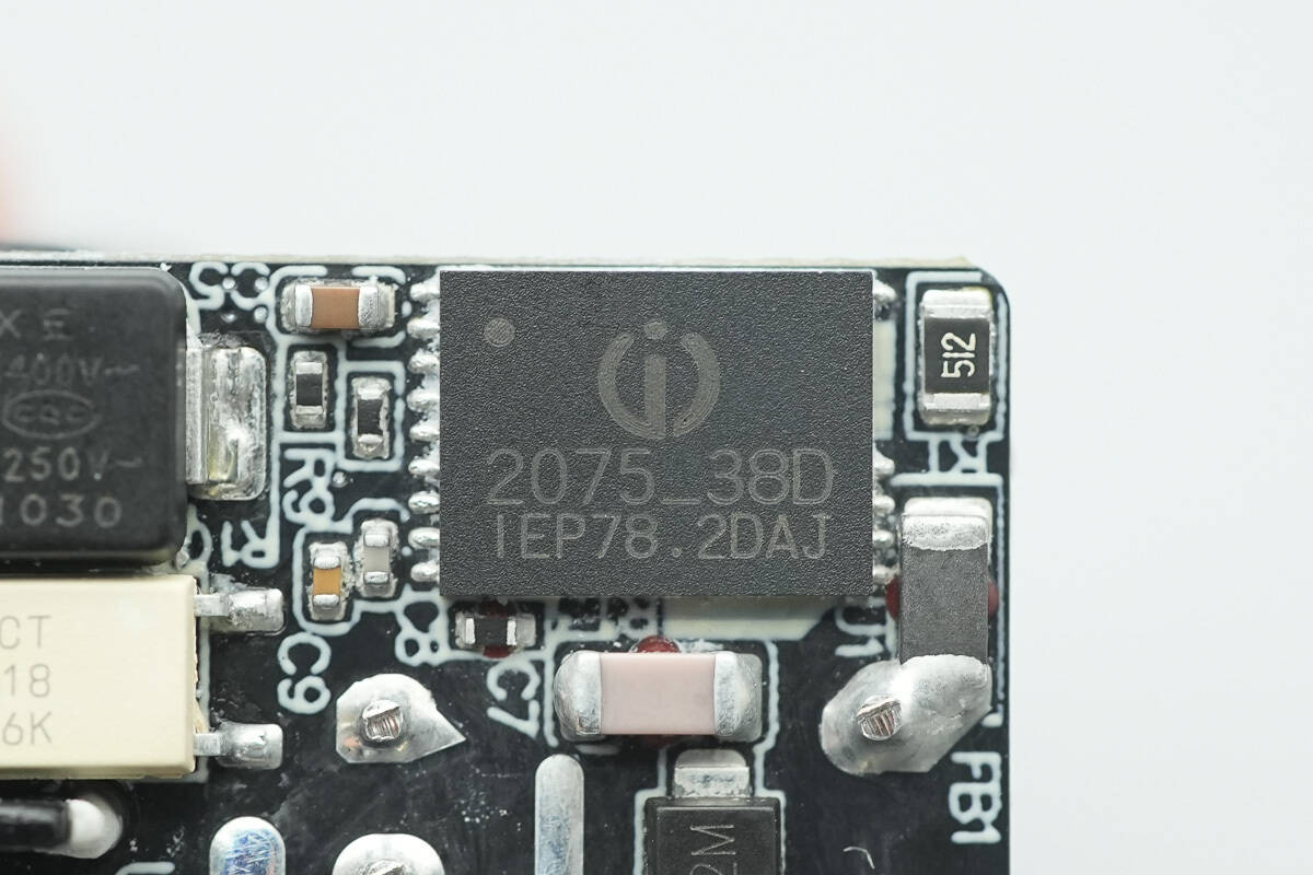
The master control chip is from Injoinic, model IP2075_38D. It is an integrated GaNFET high-performance multi-mode AC/DC flyback controller, featuring adaptive multi-mode control (MMC) and secondary-side regulation (SSR), suitable for applications requiring high power density and precise output voltage/current.
The IP2075_38D incorporates high-voltage startup, eliminating the traditional startup resistor to reduce standby power consumption. Additionally, when the AC input is removed, the HV pin discharges the X-cap, helping to minimize X-cap discharge losses and achieve ultra-low standby power. It combines frequency foldback and valley switching techniques to reduce switching losses and improve efficiency. By introducing frequency modulation, EMI emissions and common-mode noise are significantly lowered.
The IP2075_38D offers a wide adaptive switching frequency range to improve light-load efficiency. Its maximum operating frequency is optimized to minimize device temperature and enhance full-load efficiency. The minimum peak current is also carefully designed to balance standby power consumption and audio noise.

The IP2075_38D enters burst mode under light-load or no-load conditions, operating with an ultra-low current of 160 µA. This significantly reduces standby power consumption, enabling compliance with strict energy-efficiency standards such as CoC V5 and DoE VI.
It also features comprehensive protection functions and a wide range of configurable parameters, including maximum switching frequency, output overvoltage protection, output undervoltage protection, brown-in/brown-out detection, over-temperature protection, and compensated overpower protection. The chip comes in a DFN18L (6×8 mm) package.
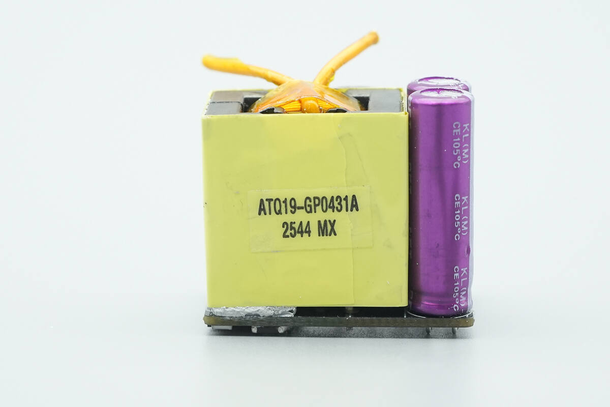
The transformer uses an ATQ19 magnetic core.
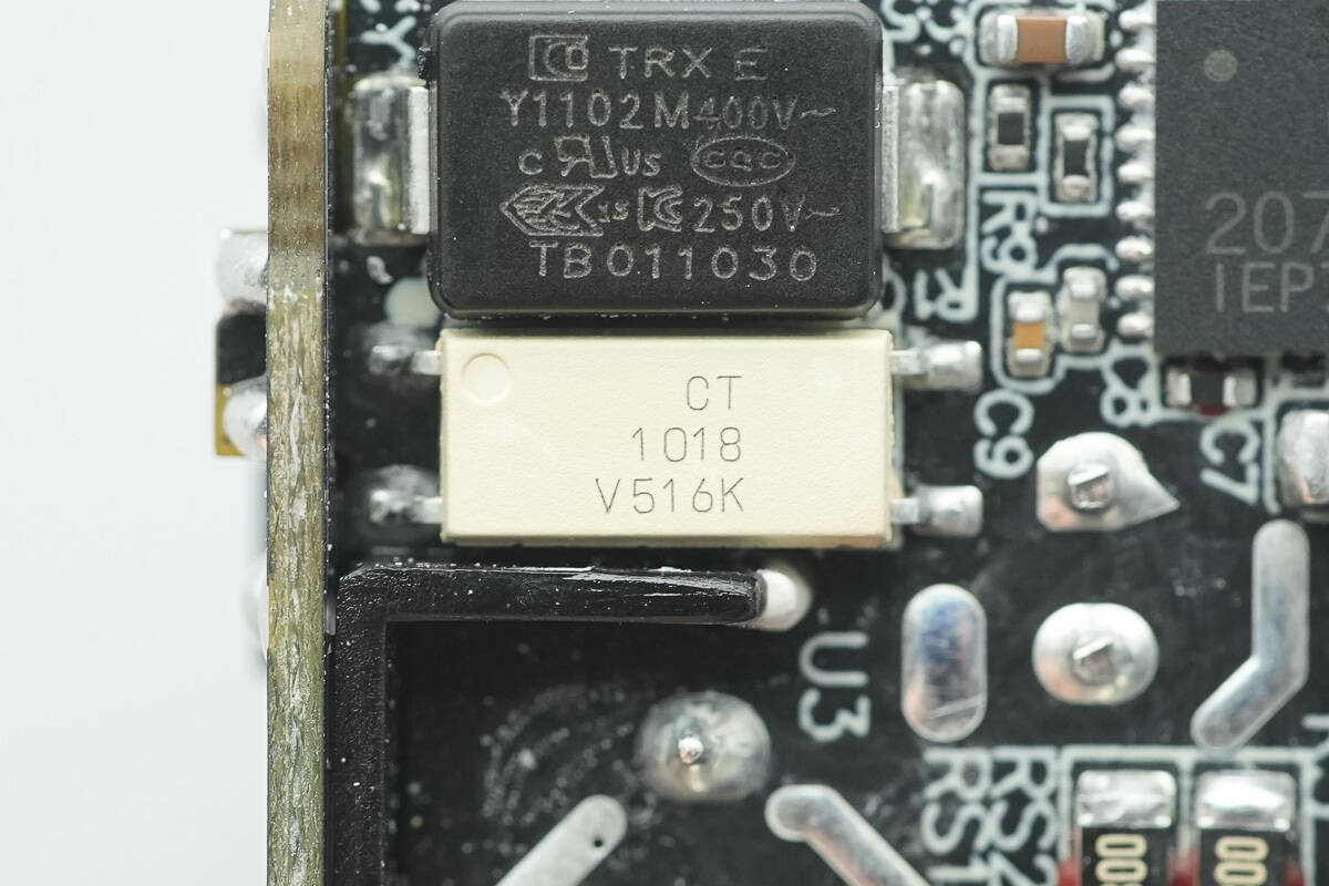
The CT1018 optocoupler is used for output voltage feedback.
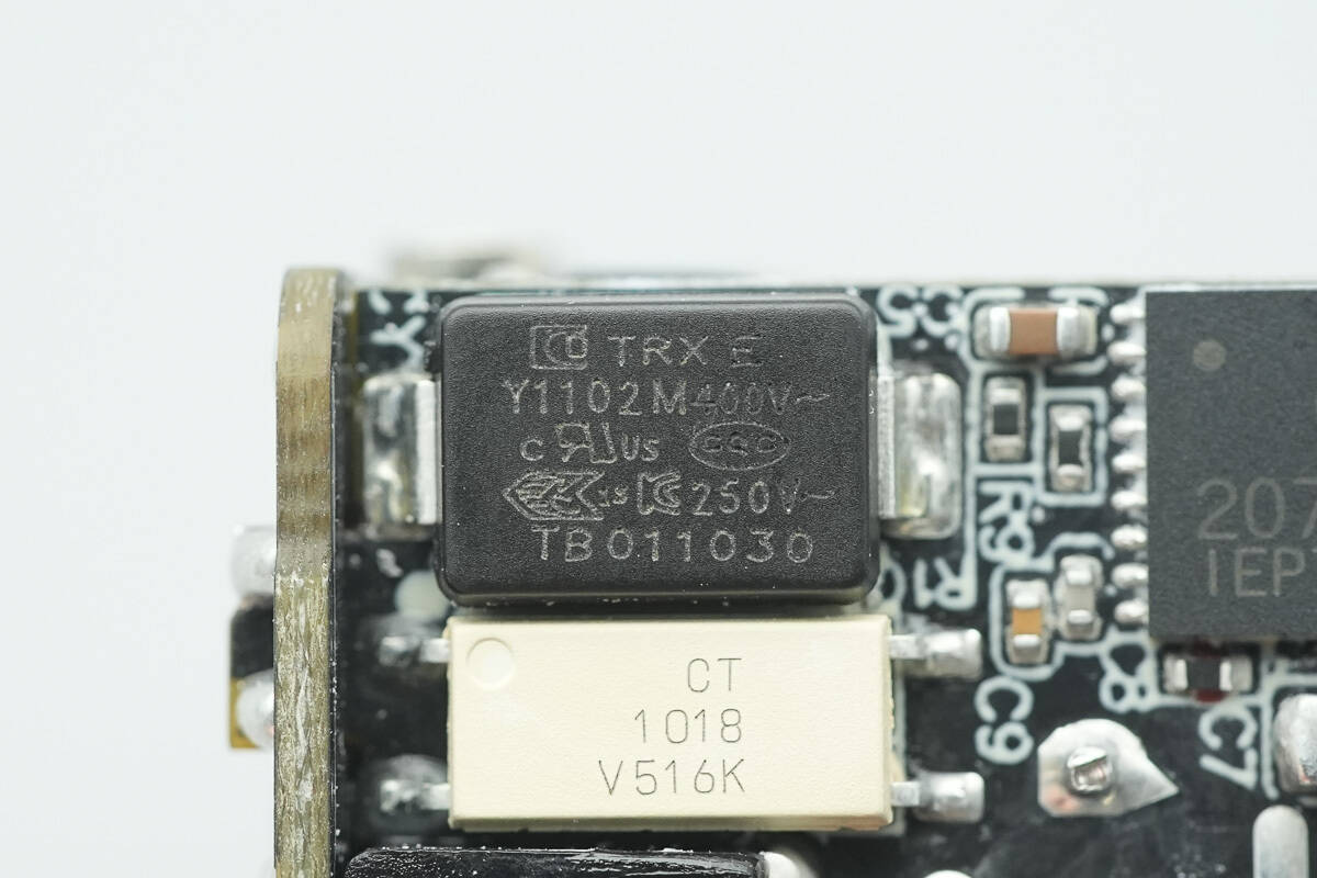
The SMD Y capacitor is from TRX, part number TMY1102M. Its compact size and light weight make it ideal for high-density power products such as GaN fast chargers.
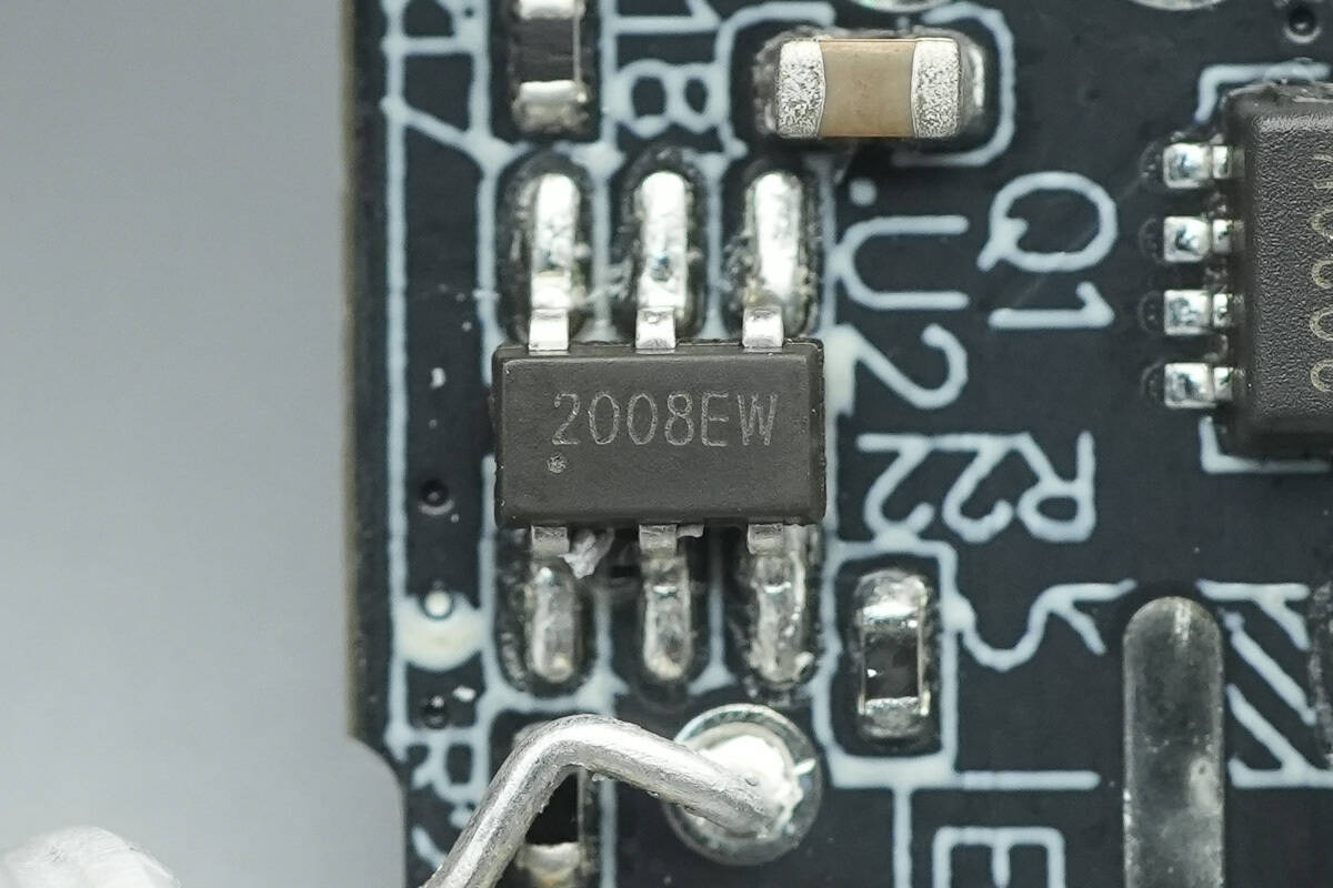
The synchronous rectifier controller is from Injoinic, model IP2008. It supports wide-voltage output systems and is used to drive the secondary-side MOSFETs in high-efficiency flyback converters, replacing Schottky diodes. By monitoring the drain-to-source voltage of the synchronous rectifier (SR) MOSFET, the IP2008 outputs optimal gate drive signals to turn the MOSFET on or off.
Using synchronous rectification significantly reduces the power loss of the secondary-side rectifier, achieving higher efficiency, lower temperature rise, and greater power density. With minimal external components, the IP2008 provides a high-performance solution for output voltages ranging from 3.3 V to 21 V.

The IP2008 does not require power from an auxiliary winding; its internal regulation circuit generates the appropriate supply voltage. This makes it suitable for charger applications with low output voltage requirements or adapters using high-side synchronous rectification.
To ensure fast MOSFET turn-off, as the secondary current decreases, the IP2008 lowers the MOSFET drive voltage to adjust the conduction voltage drop to around 40 mV and rapidly turns off the MOSFET before the drain-to-source voltage reverses. A configurable ringing-detection circuit prevents false triggering caused by V_DS ringing in discontinuous conduction mode (DCM) or quasi-resonant operation. The IP2008 comes in a SOT23-6 package.
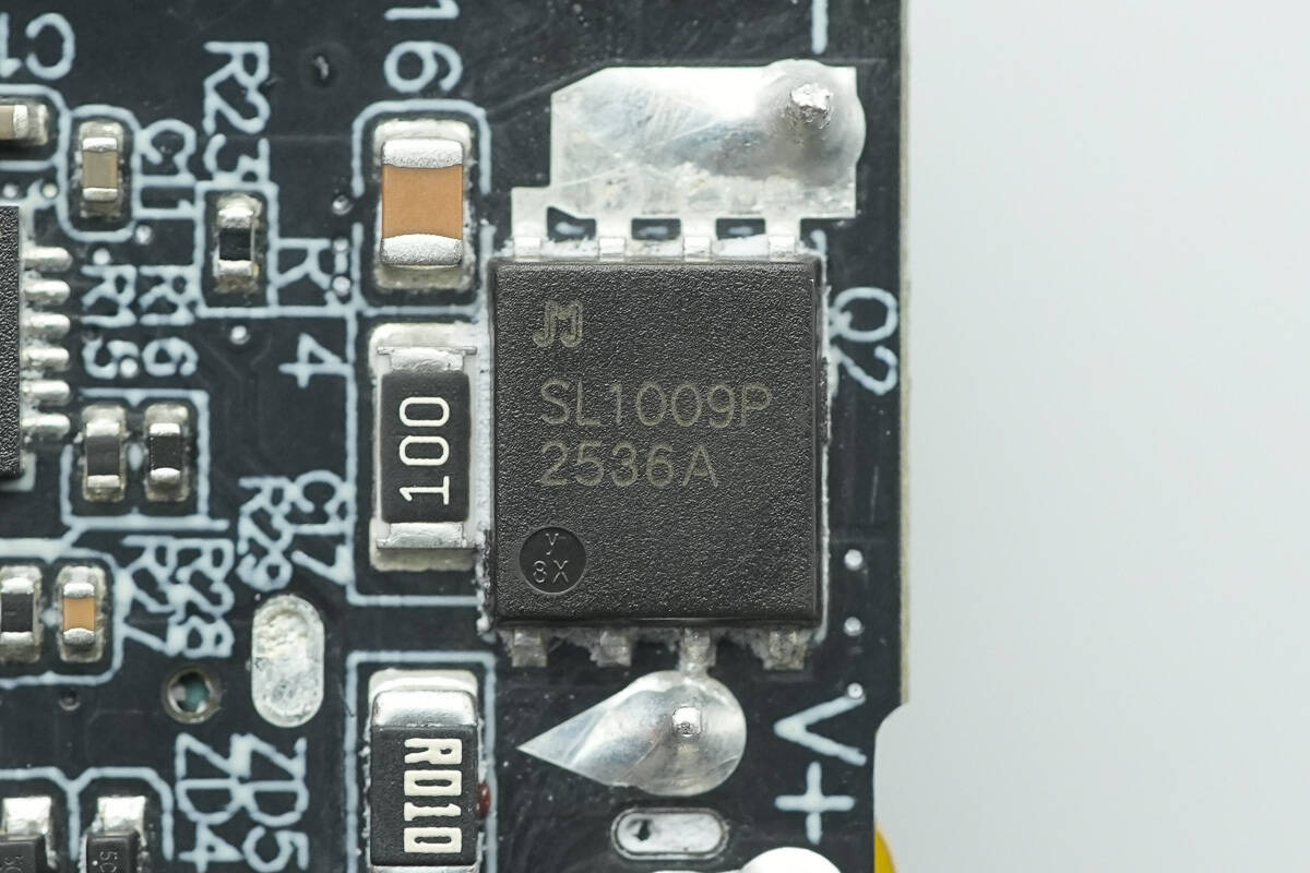
The synchronous rectifier is from JJWD, model JMSL1009PG. It is an N‑MOSFET with a 40 V voltage rating and 5.6 mΩ on-resistance, packaged in a PDFN 5×6‑8L form factor.
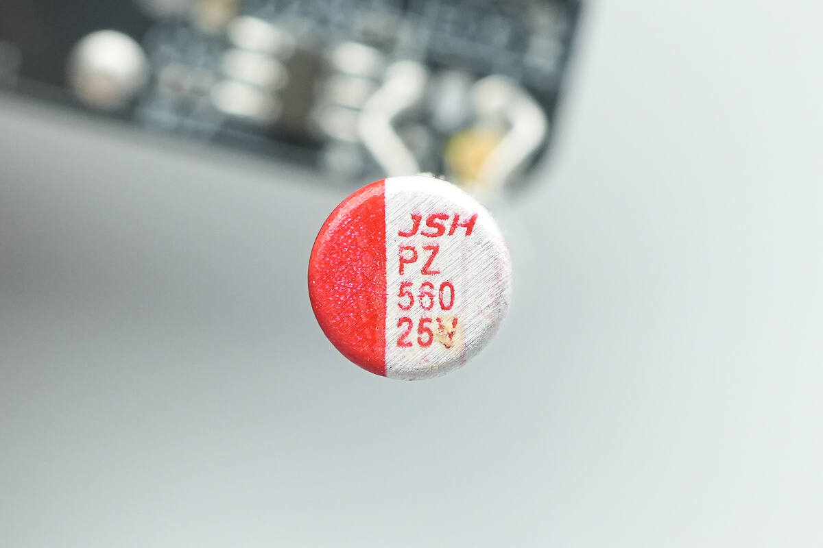
The solid capacitor for output filtering is from JSH, rated at 25 V 560 µF.
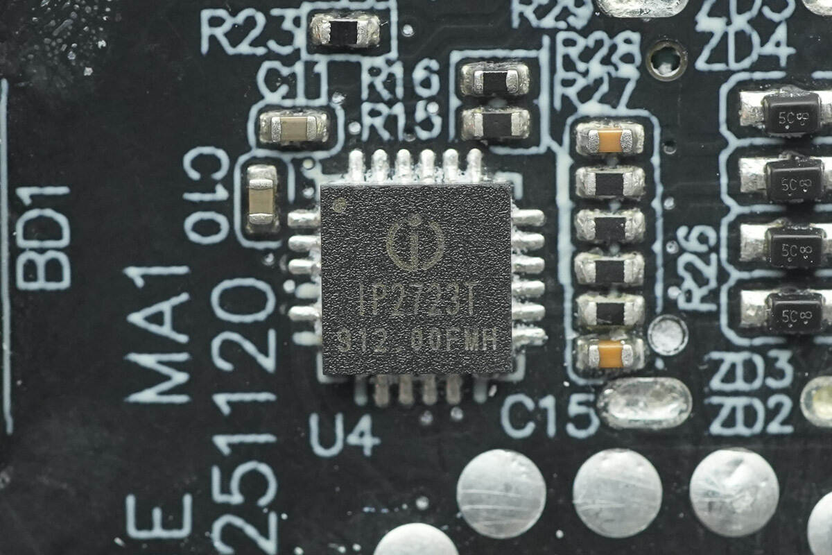
The protocol chip is also from Injoinic, model IP2723TH. It is an integrated fast-charging protocol IC for USB output ports, supporting multiple protocols including USB Type-C DFPTM, PD 2.0/PD 3.2/PPS/SPRAVS, HVDCP QC 4/4+/3.0/2.0, FCP, SCP, AFC, MTK PE+ 2.0/1.1, Apple 2.4 A, BC1.2, and Samsung 2.0 A. It provides a complete Type-C solution for adapters, car chargers, and other single-output applications.
The IP2723TH features high integration and rich functionality, requiring very few external components in applications. This effectively reduces the overall solution size and lowers BOM cost. The chip comes in a QFN24 package.
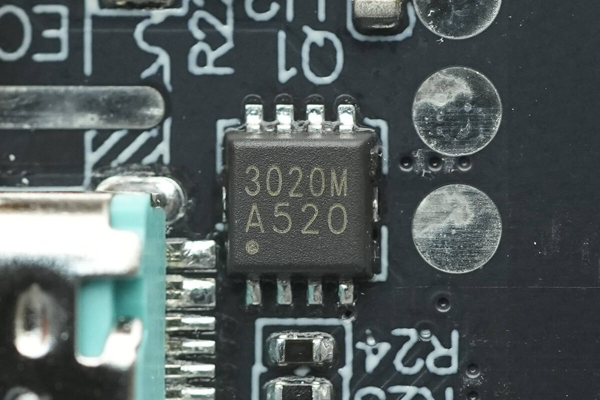
The VBUS MOSFET is marked 3020M and comes in a DFN 3×3 mm package.
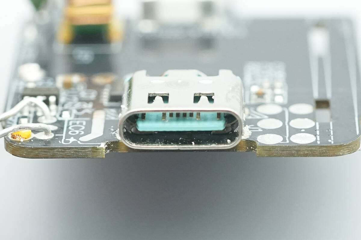
Close-up of the USB-C socket.

Well, those are all components of the MIIIW 45W Mini Magic Cube GaN Charger.
Summary of ChargerLAB
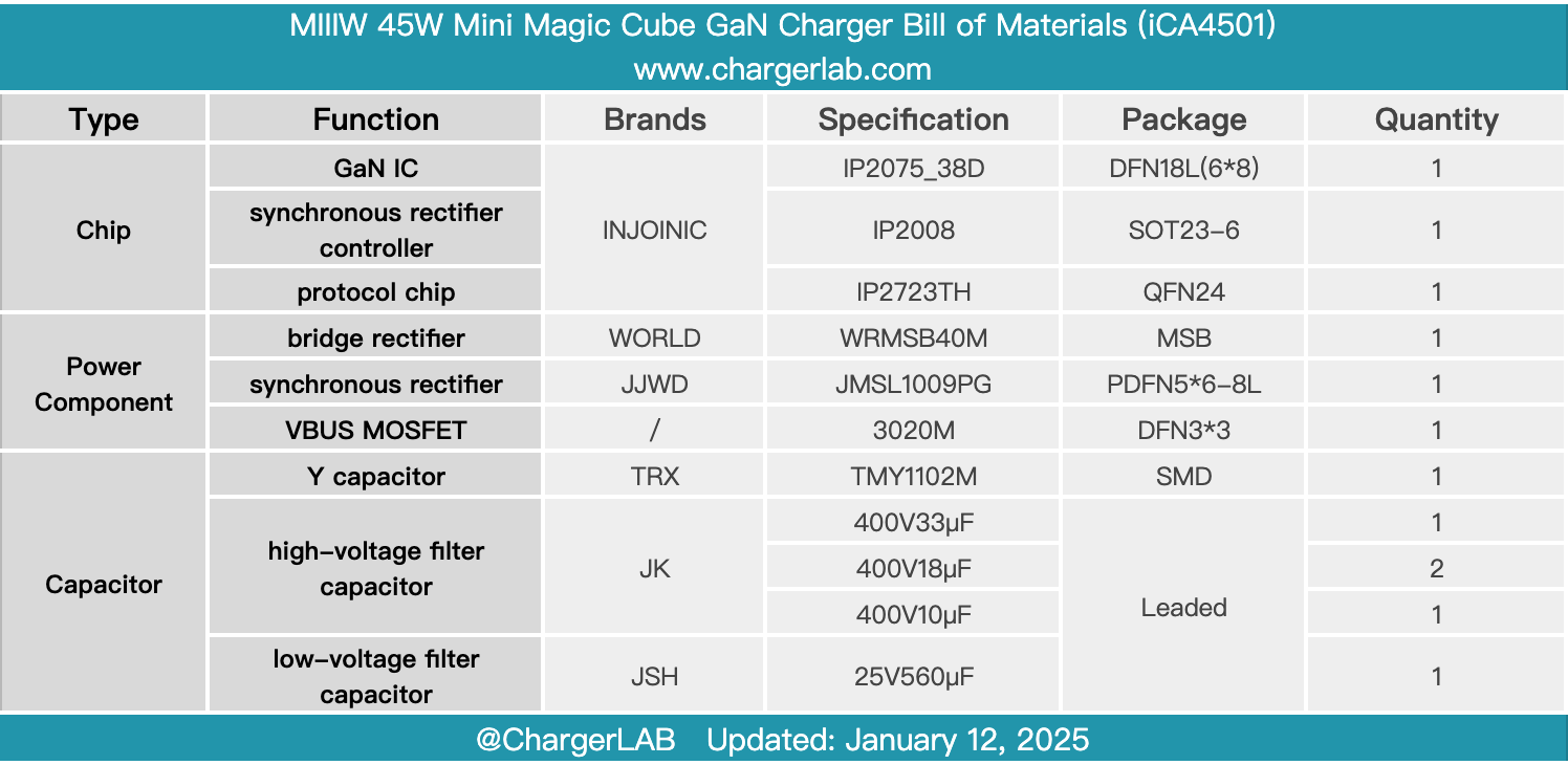
Here is the component list of the MIIIW 45W Mini Magic Cube GaN Charger for your convenience.
It features a silver-gray color scheme with a metallic finish. In terms of size, it is comparable to the Xiaomi 45W Little Pudding fast charger, while offering a more visually appealing design. It supports 45 W PD/PPS fast charging, Xiaomi 48 W Surge fast charging, and Huawei 22.5 W SCP fast charging, among others.
After taking it apart, we found that it adopts two PCBs stacked together and employs a complete Injoinic power solution with the IP2075_38D, IP2008, and IP2723TH. This solution is not only market-proven, mature, and reliable, but also perfectly suited to MIIIW products that have stringent space requirements.
Related Articles:
1. Teardown of AOHi THE FUTURE AI PD GaN+ 170W 3-Port LED Display Fast Car Charger (AOC-S009)
2. Teardown of Torras FlexLine 67W Charger (CQ10)
3. Teardown of Anker Prime 150W Charging Station (A1903)