Introduction
Recently, MECHREVO released a 140W GaN power adapter. It supports MECHREVO’s proprietary 20V/7A 140W fast-charging protocol, designed to meet the power demands of the brand’s laptops equipped with 50-series GPUs—whether for light gaming or intensive office workloads. In addition to proprietary fast charging, it also supports 100W USB Power Delivery, along with compatibility for QC, SCP, PPS, and other protocols, offering excellent versatility across devices. Next, we’ll take a closer look at its internal design and components.
Product Appearance
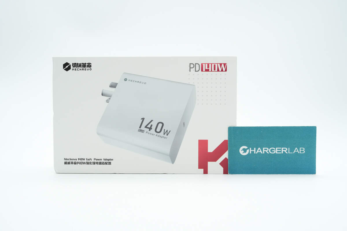
The front of the box displays the MECHREVO logo, product name, charger image, and “PD 140W”.
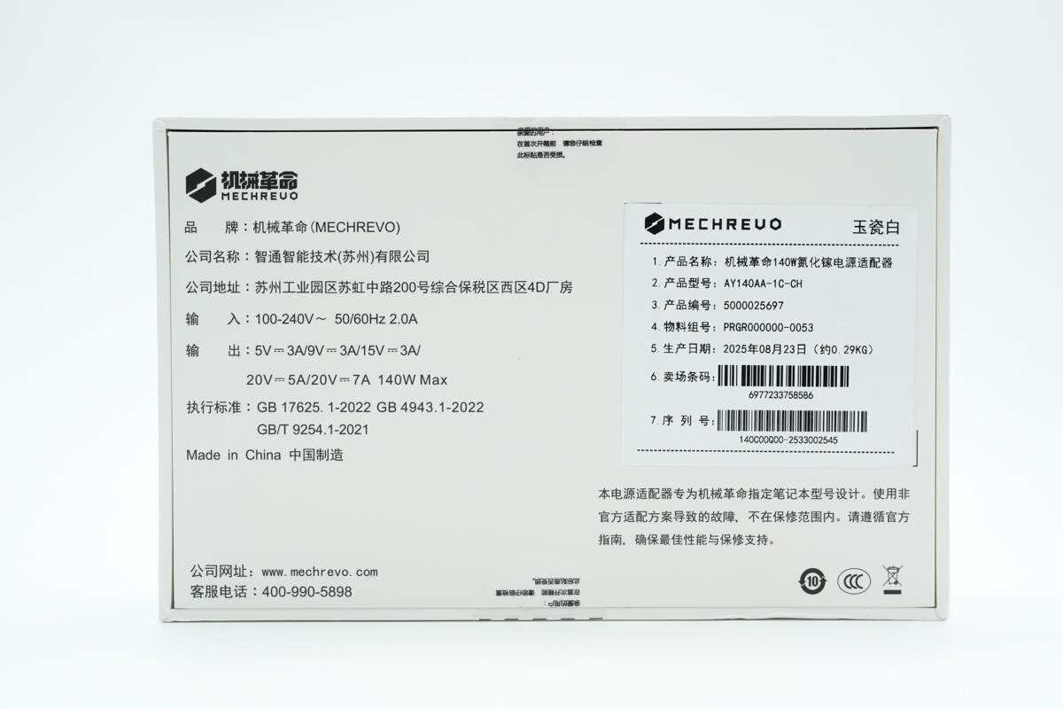
The back displays the specifications.
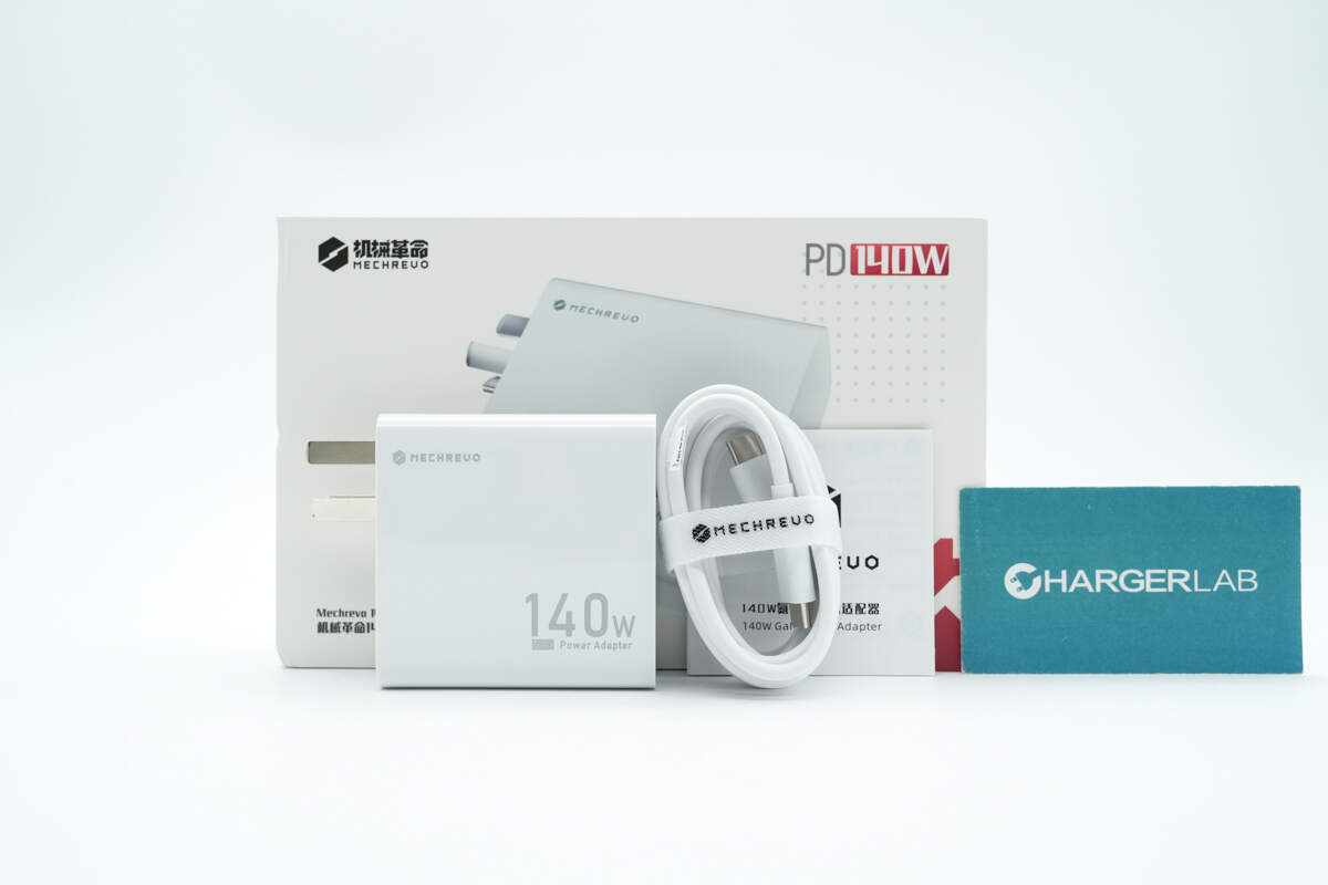
The package includes the charger, a cable, and a user manual.
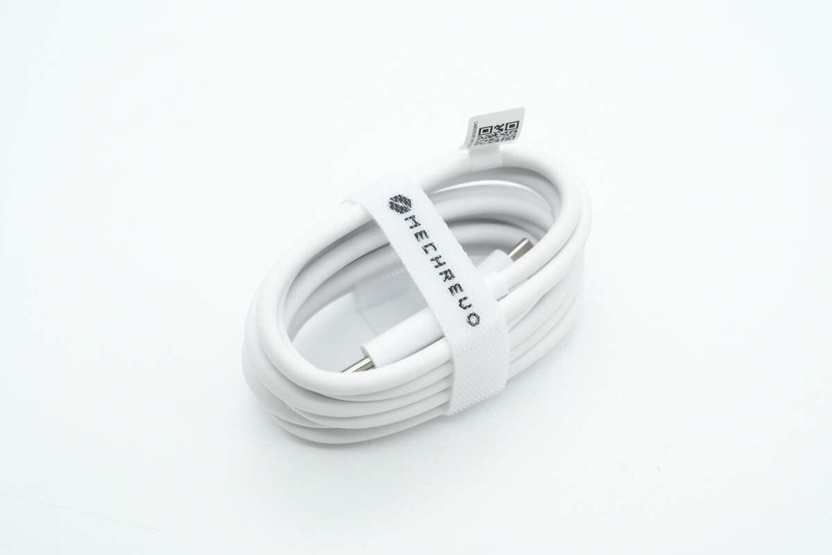
The included cable is secured with a MECHREVO-branded Velcro strap.
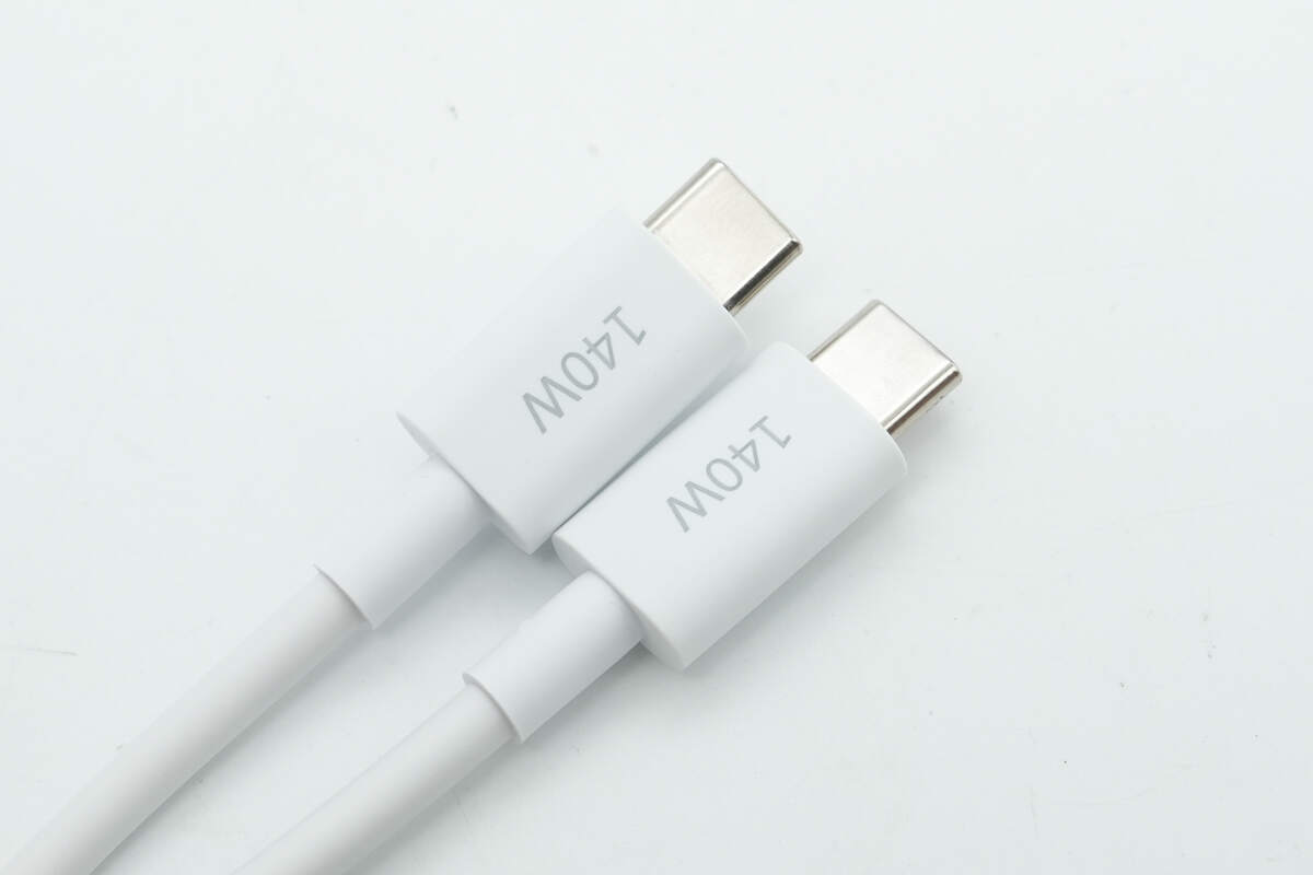
The cable is a dual USB-C type, with “140W” printed on the connectors.
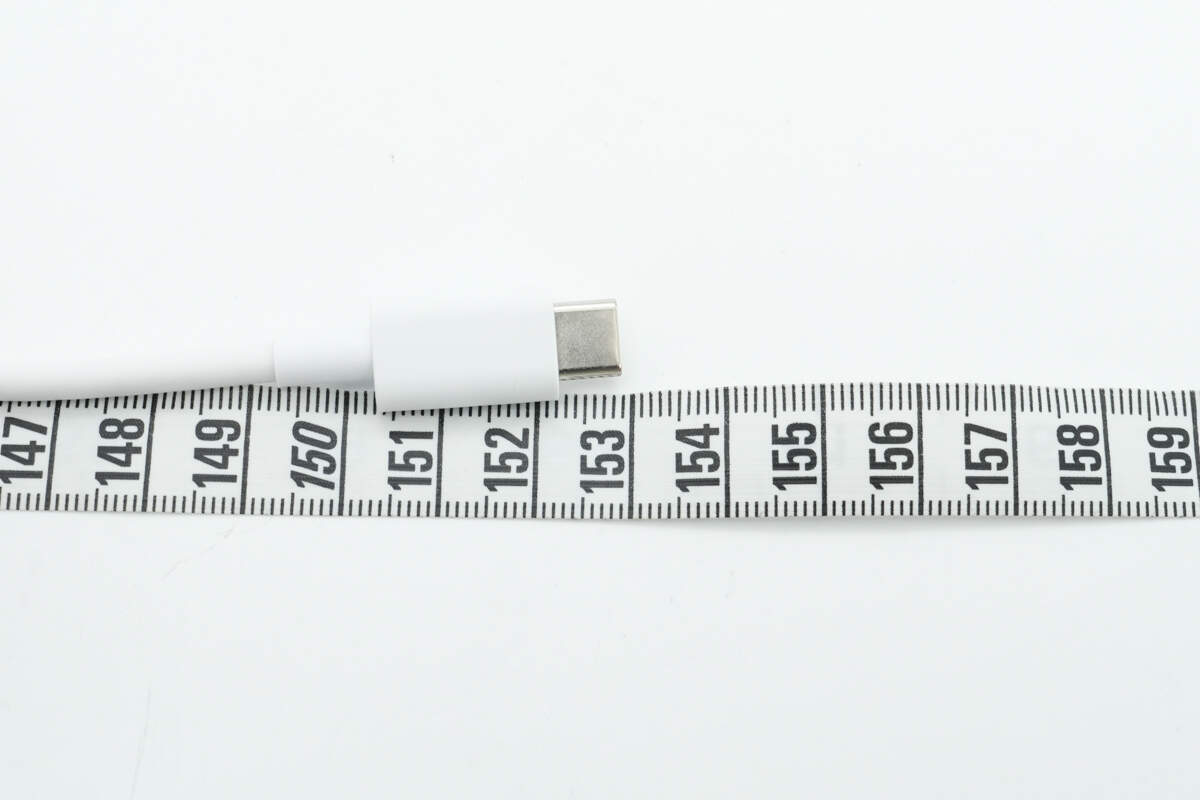
The length of the cable is about 153 cm (60.24 inches).

ChargerLAB POWER-Z KM003C shows it has an E-marker chip, supporting not only MECHREVO’s proprietary 20V/7A 140W fast charging but also backward compatibility with 20V/5A fast charging. Additionally, the cable supports USB 2.0 data transfer speeds.
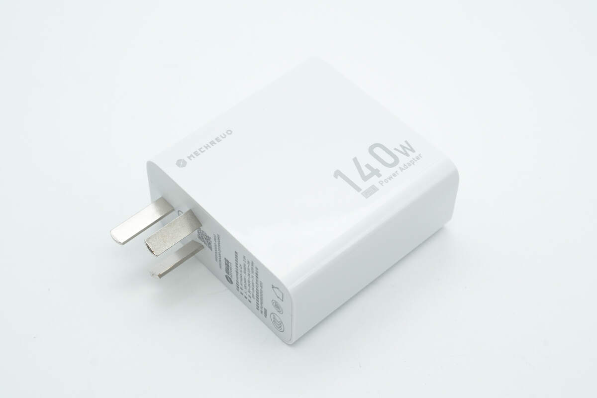
The charger housing is made of flame-retardant PC material with a smooth surface.
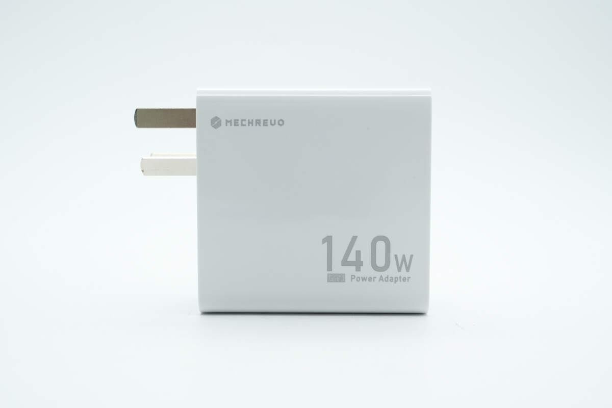
The front is printed with “MECHREVO” and “140W GaN Power Adapter.”
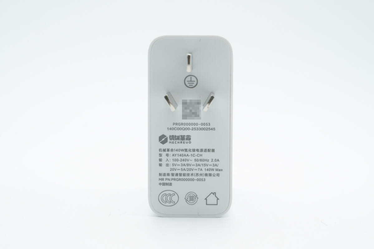
The input housing is printed with the specification information.
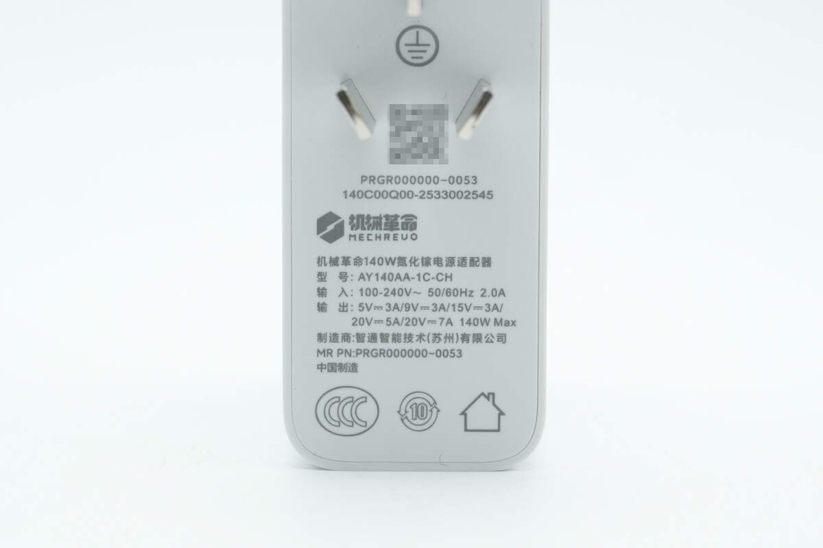
Model: AY140AA-1C-CH
Input: 100-240V\~50/60Hz 2.0A
Output: 5V 3A, 9V 3A, 15V 3A, 20V 5A, 20V 7A 140W Max
PPS: 3.3-21V 5A 100W Max
The charger is CCC certified.
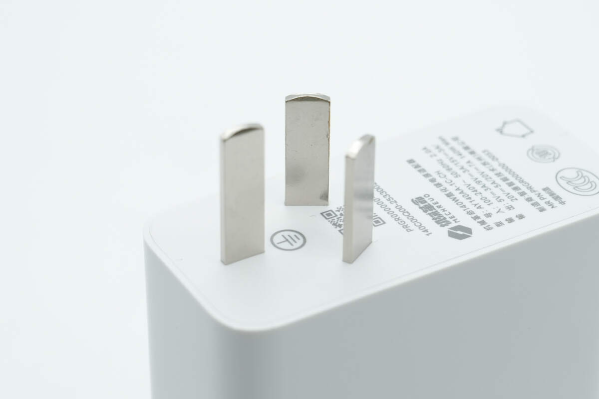
It is equipped with a fixed plug.
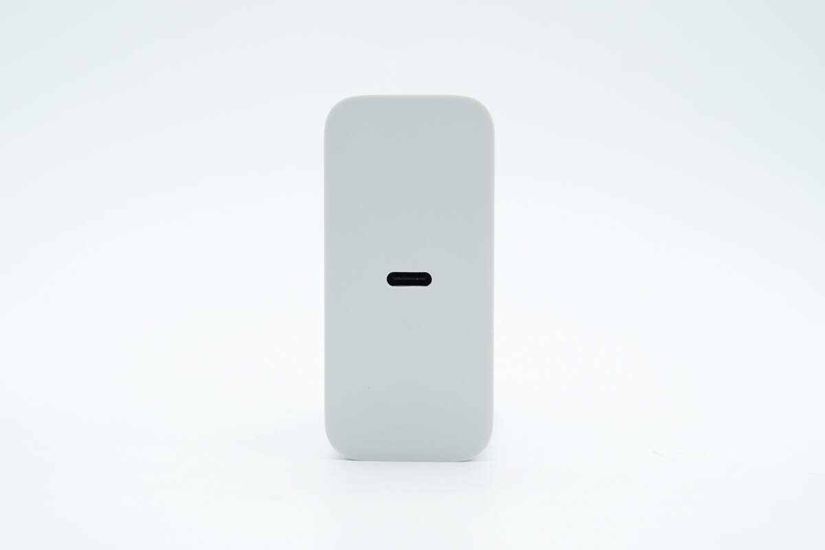
The output USB-C port is centered.
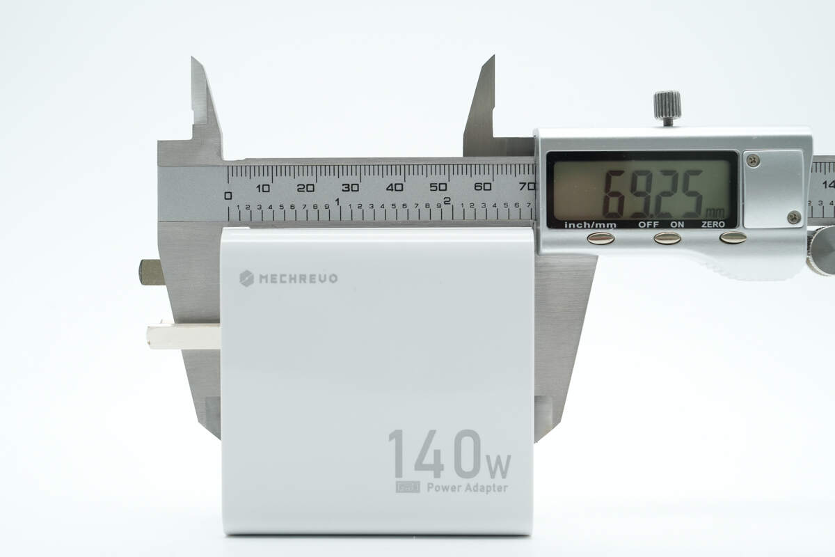
The length of the charger is about 69.25 mm (2.73 inches).
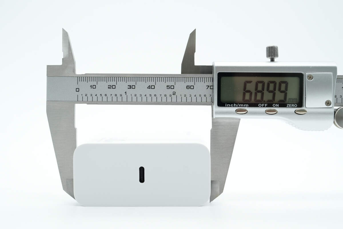
The width is about 68.99 mm (2.72 inches).
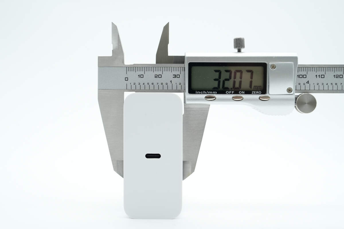
The thickness is about 32.07 mm (1.26 inches).
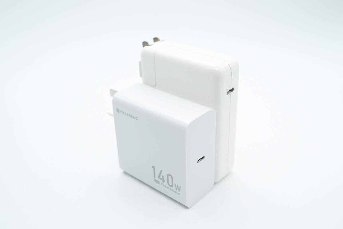
It is slightly smaller in size than the Apple 140W charger.
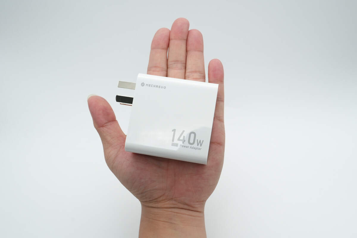
That's how big it is in the hand.
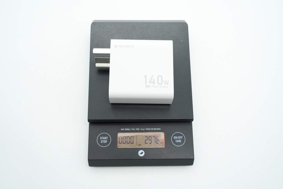
The weight is about 298 g (10.51 oz).
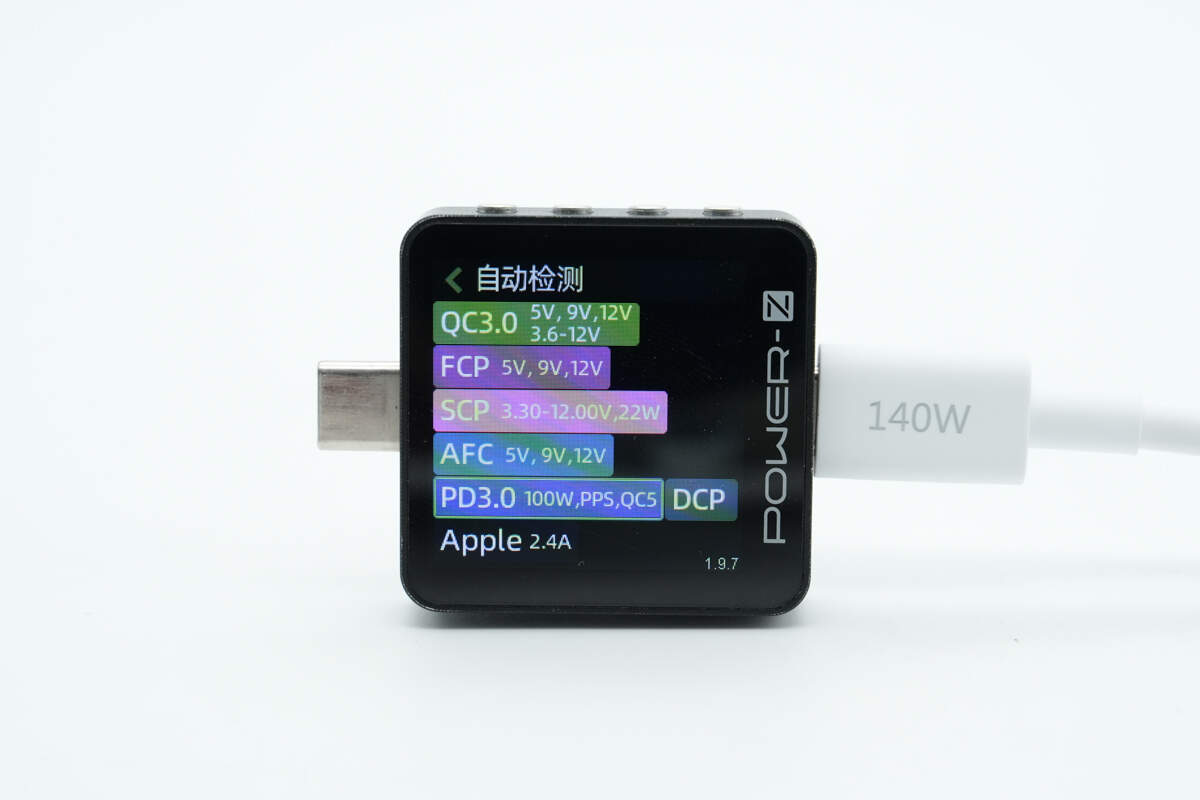
ChargerLAB POWER-Z KM003C shows that it supports QC3.0/5, FCP, SCP, AFC, PD3.0, PPS, DCP, and Apple 2.4A charging protocols.
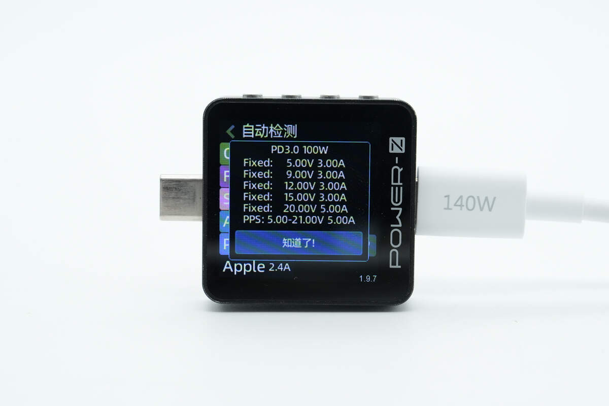
And it has five fixed PDOs of 5V3A, 9V3A, 12V3A, 15V3A, and 20V5A. It has one set of PPS, which is 5-21V5A.
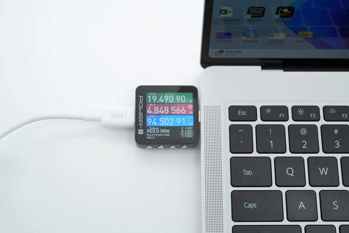
When used to charge the Huawei MateBook X Pro, the charging power is about 94.5W, successfully activating the 20V/5A 100W charging protocol.
Teardown
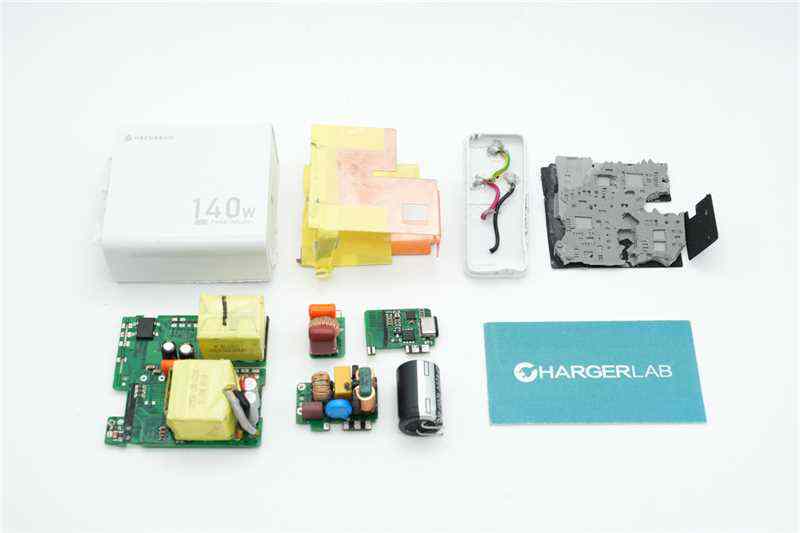
Next, let's take it apart to see its internal components and structure.
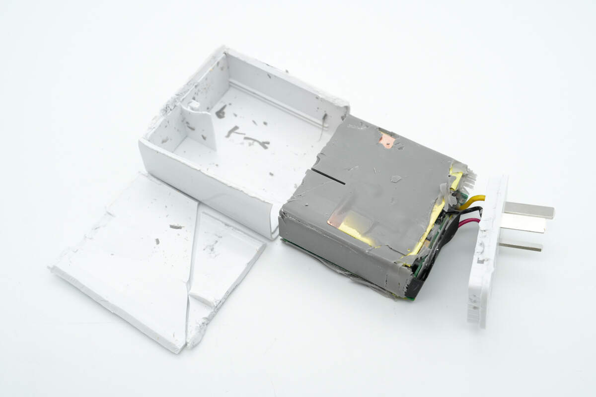
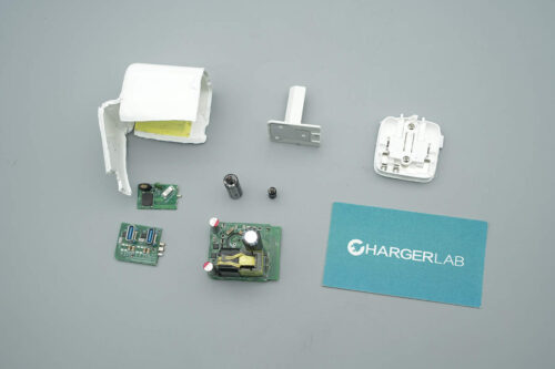
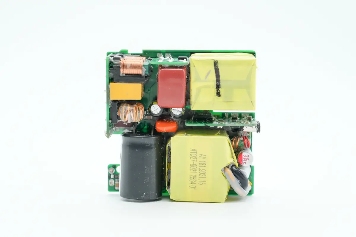
Cut open the housing and remove the PCBA module. The module is encapsulated with potting compound to improve weather resistance and heat dissipation. The input pins are soldered to the PCBA using wires.
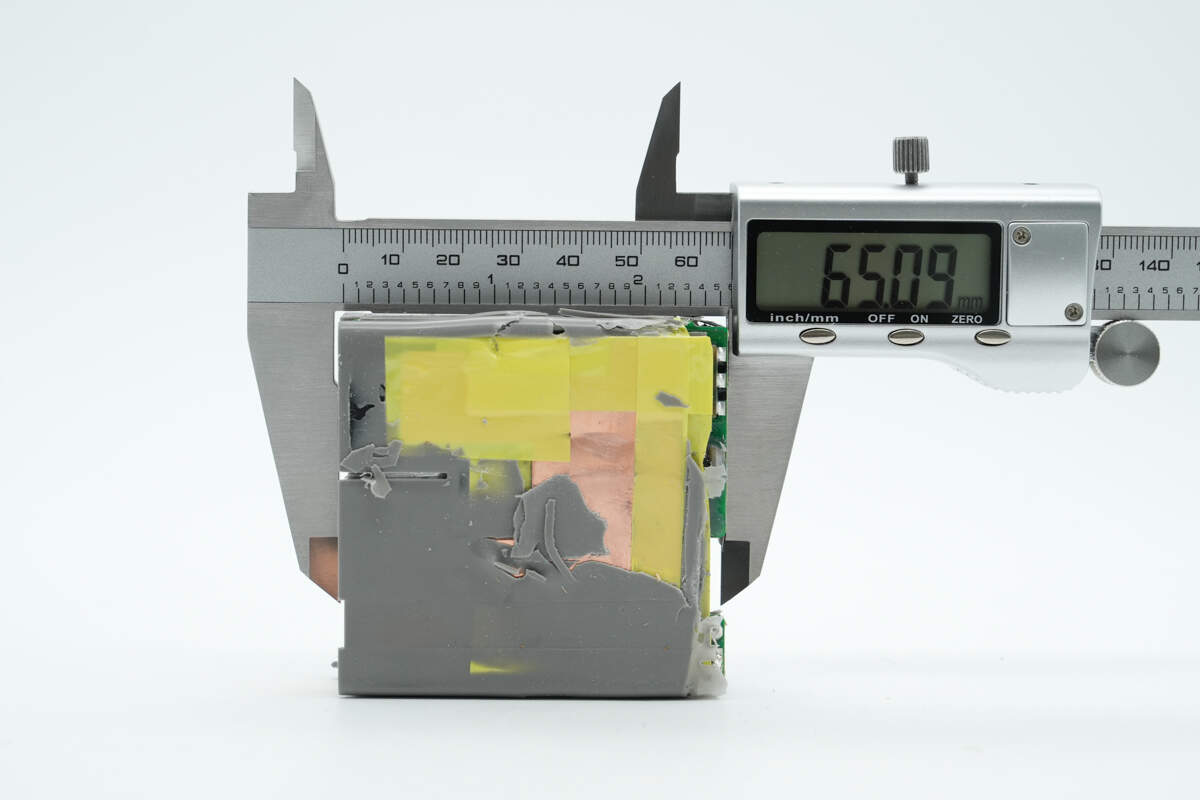
The PCBA module measures approximately 65.09 mm (2.56 inches) in both length and width.
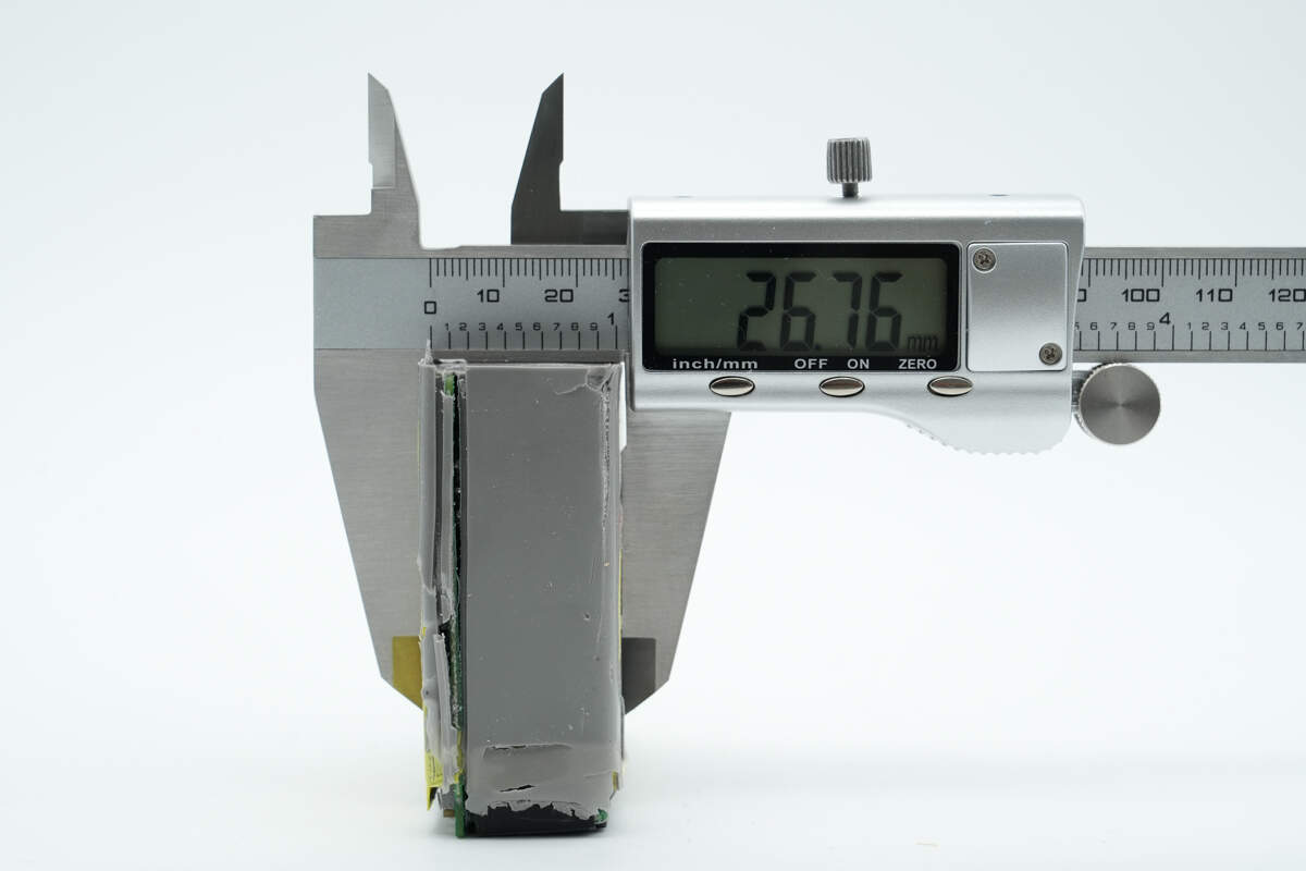
The thickness is about 26.76 mm (1.054 inches).
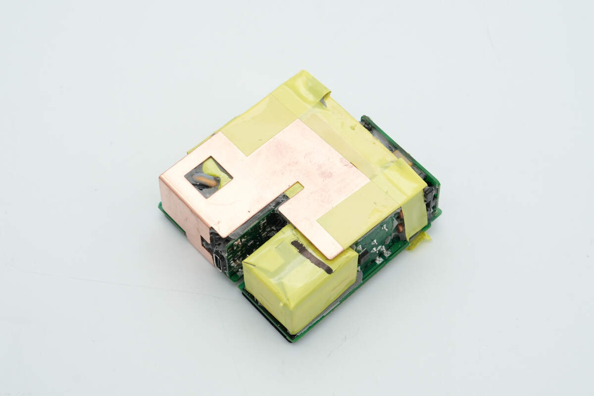
Remove the thermal compound from the PCBA module. The top side of the PCBA is covered with a copper heatsink.
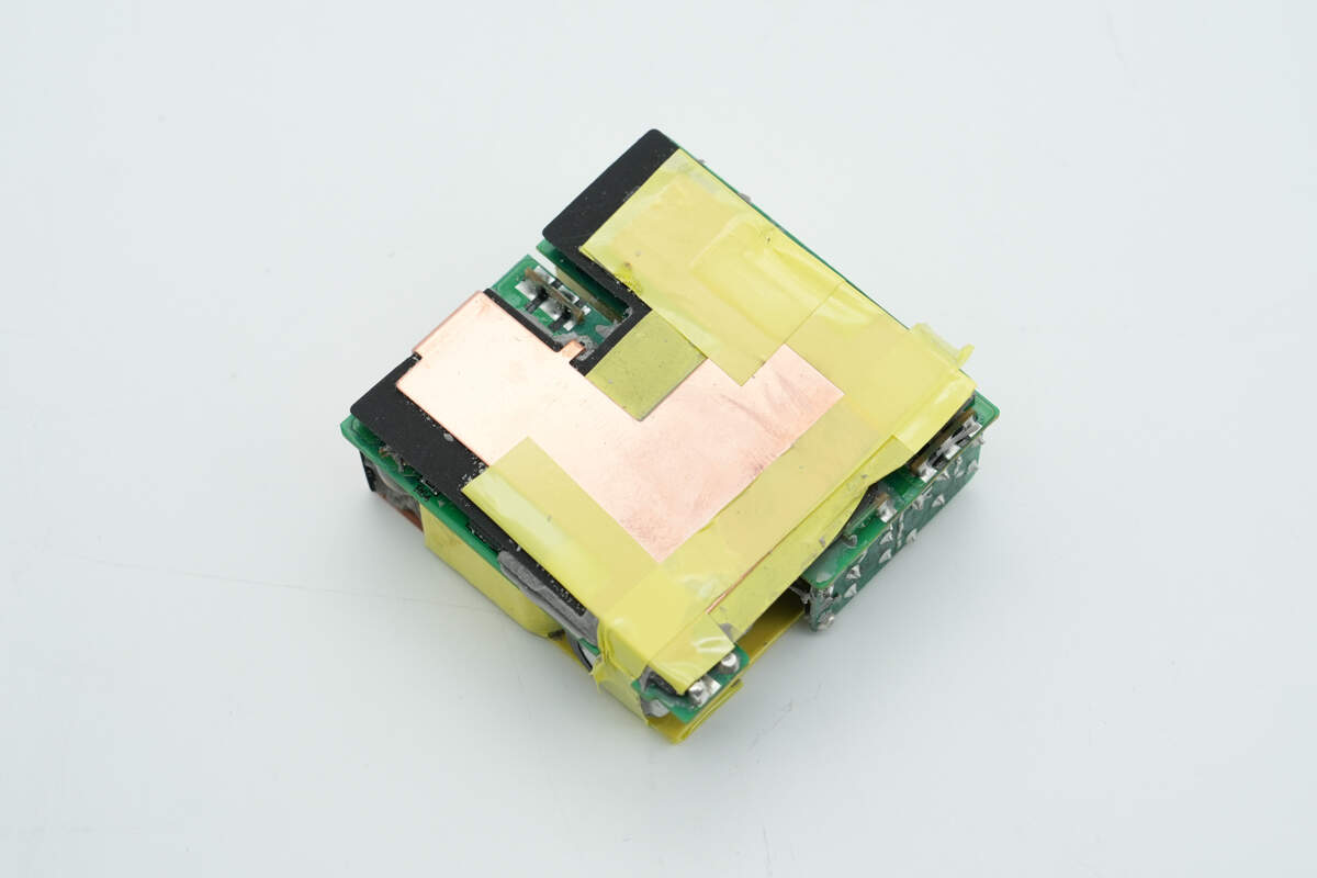
The bottom side is also covered with a copper heatsink, insulated with a Mylar sheet.
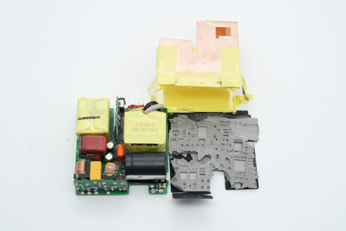
After removing the copper heatsinks and Mylar sheet, it’s revealed that the heatsinks on both sides are part of an integrated one-piece design.
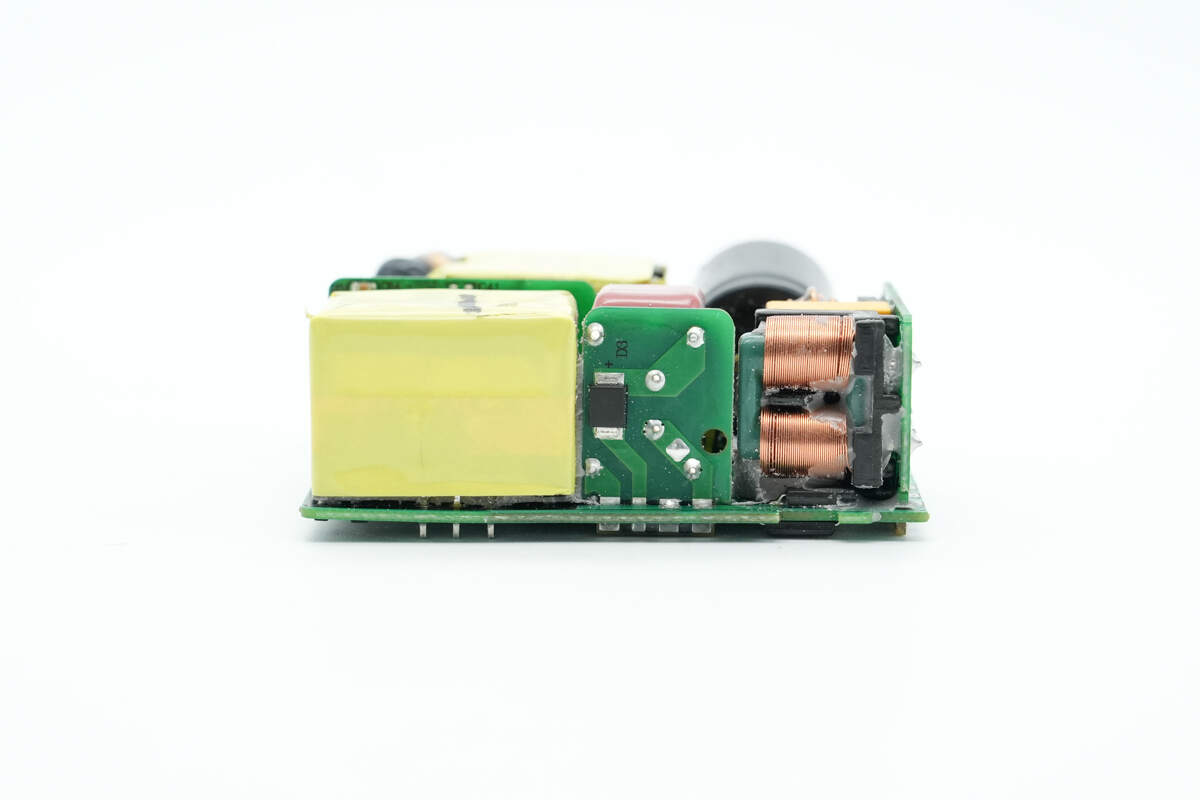
The front side of the PCBA module features three separate small PCBs, which are used for mounting the time-delay fuse, common mode chokes, film capacitors, and the USB-C socket.
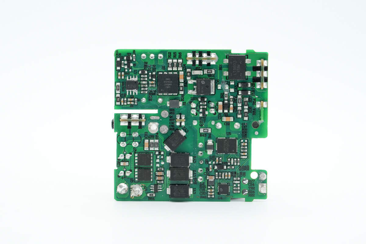
The upper area on the back side houses the bridge rectifiers, PFC controller, PFC boost MOSFET, and PFC rectifier. The lower area contains the master control chip along with the corresponding power MOSFETs, as well as four SMD Y-capacitors.
The back side of the small front-end PCBs on the PCBA module has no components.
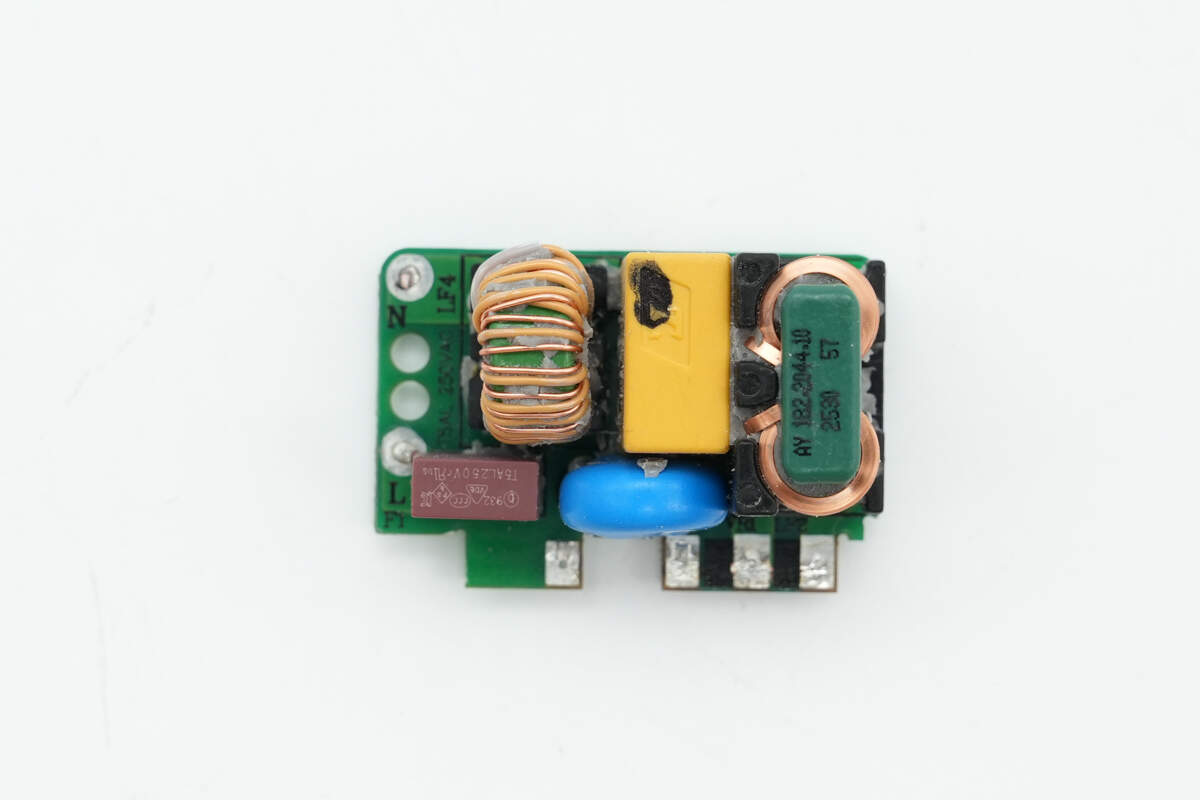
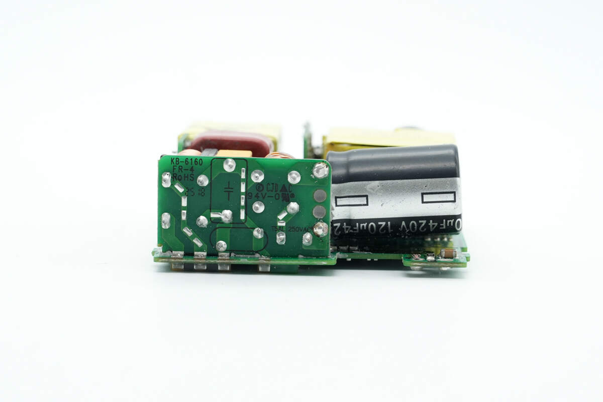
Remove the small PCB. The front has a time-delay fuse, a varistor, common mode chokes, and a safety X2 capacitor.
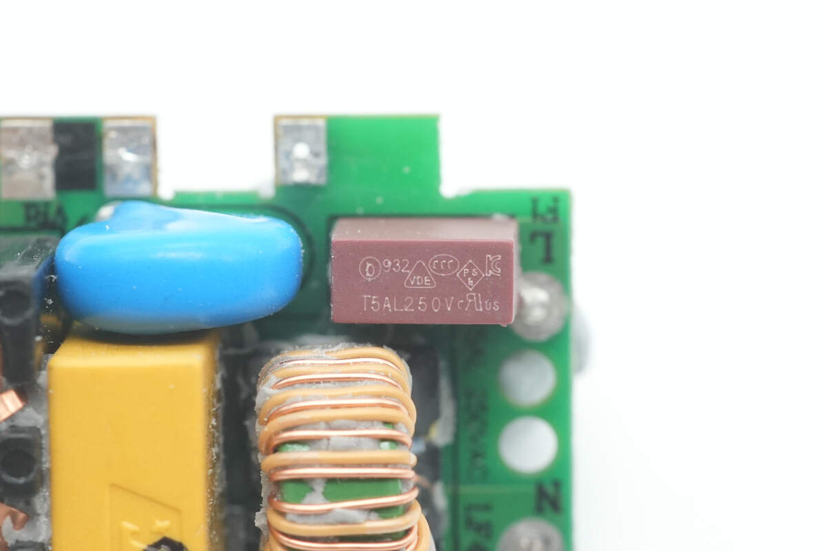
The time-delay fuse is manufactured by Betterfuse, model 932, rated at 5A 250V.

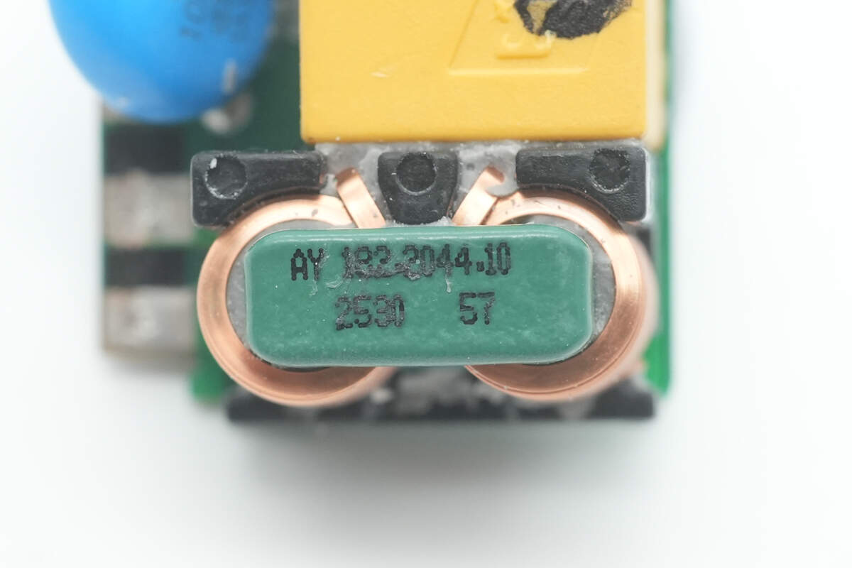
The varistor is from HEL, model 10D681K, used for surge overvoltage protection.
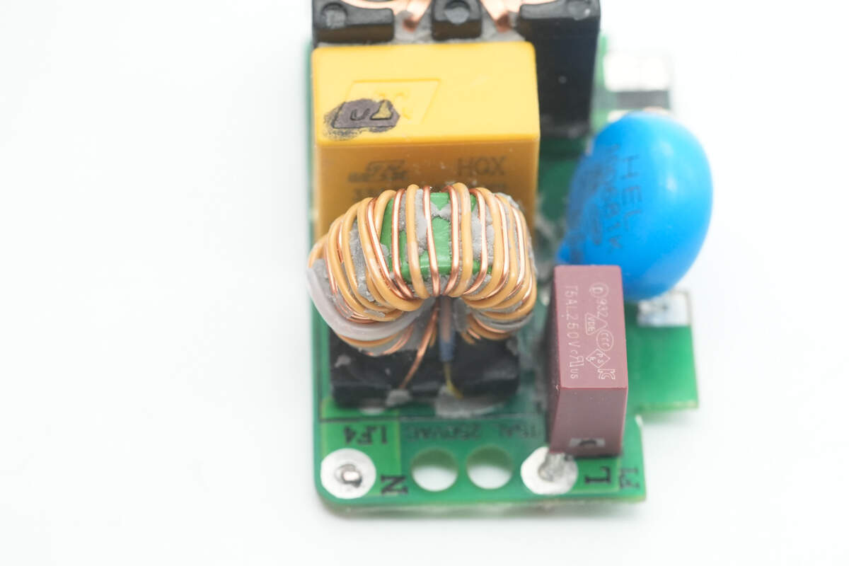
The common mode choke features a two-stage design to filter out EMI interference, with the first coil wound using dual wires.
The second choke uses a green magnetic core and is wound with flat copper tape.
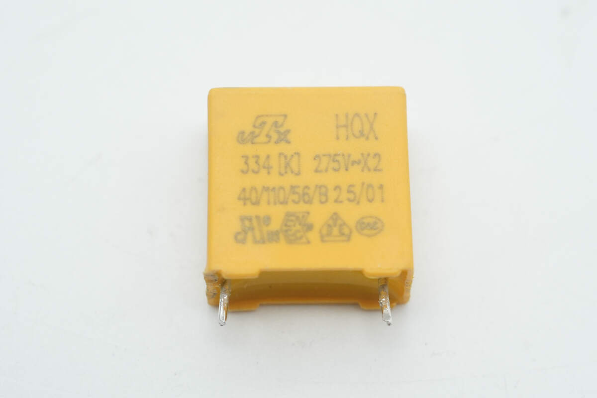
The safety X2 capacitor has a capacitance of 0.33μF.

The bridge rectifier is from LITEON, model TT8M, rated at 1000V 8A, and uses an HBS package.

Another bridge rectifier with the same model number is located on the back side.
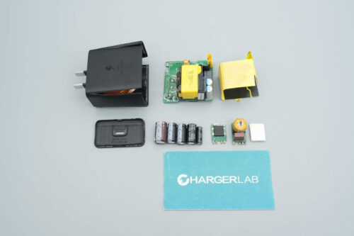
The side is soldered with a filter PCB and the PFC boost inductor. There is a diode on the back side of the small PCB.
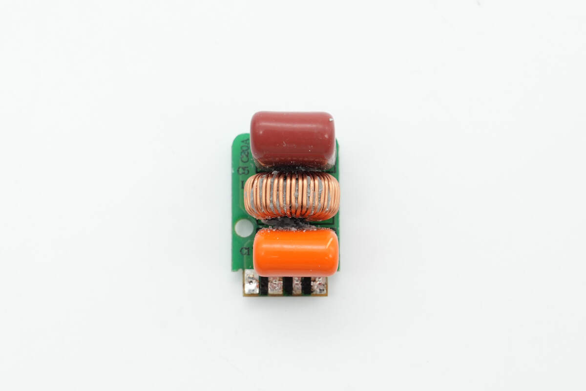
Remove the small PCB. The front side has two film capacitors and one filter inductor.
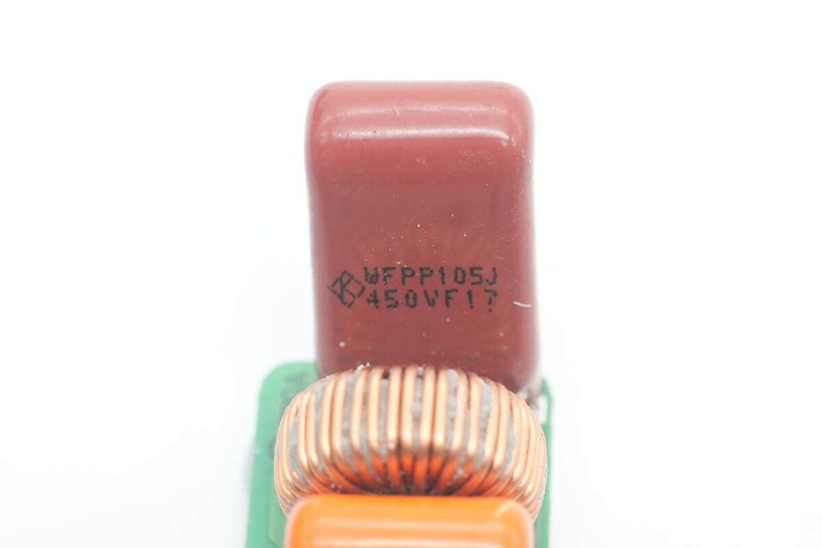
The red film capacitor is rated at 1μF, 450V.
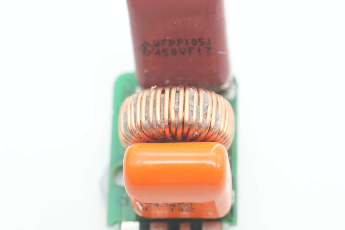
Close-up of the filter inductor.
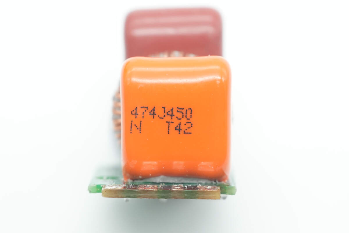
The orange film capacitor is rated at 0.47μF, 450V.

The PFC controller is from JOULWATT, model JW1572. It is a boost-type PFC controller featuring high-precision constant voltage output, designed for single-stage power factor correction. It uses constant on-time control to ensure a high power factor without the need for an input voltage detection circuit, simplifying system design and reducing losses.
Operating in critical conduction mode, it reduces switching losses while improving EMI performance and efficiency. The controller offers comprehensive protection functions, including feedback open-circuit protection, current sense resistor short-circuit protection, cycle-by-cycle overcurrent protection, feedback overvoltage protection, and overtemperature protection. It is well-suited for USB PD fast charging, LCD TVs, and monitor applications.

Here is the information about JOULWATT JW1572.

The PFC boost MOSFET is from Innoscience, model INN650D150A. It is a high-voltage GaN transistor with a voltage rating of 650V and a transient withstand voltage of 750V, featuring an on-resistance of 150mΩ. It comes in a DFN 8×8 package.
The INN650D150A supports ultra-high switching frequencies, has no reverse recovery charge, and boasts very low gate charge and output charge. It meets JEDEC standards for industrial applications, includes built-in ESD protection, and complies with RoHS, lead-free, and EU REACH regulations.
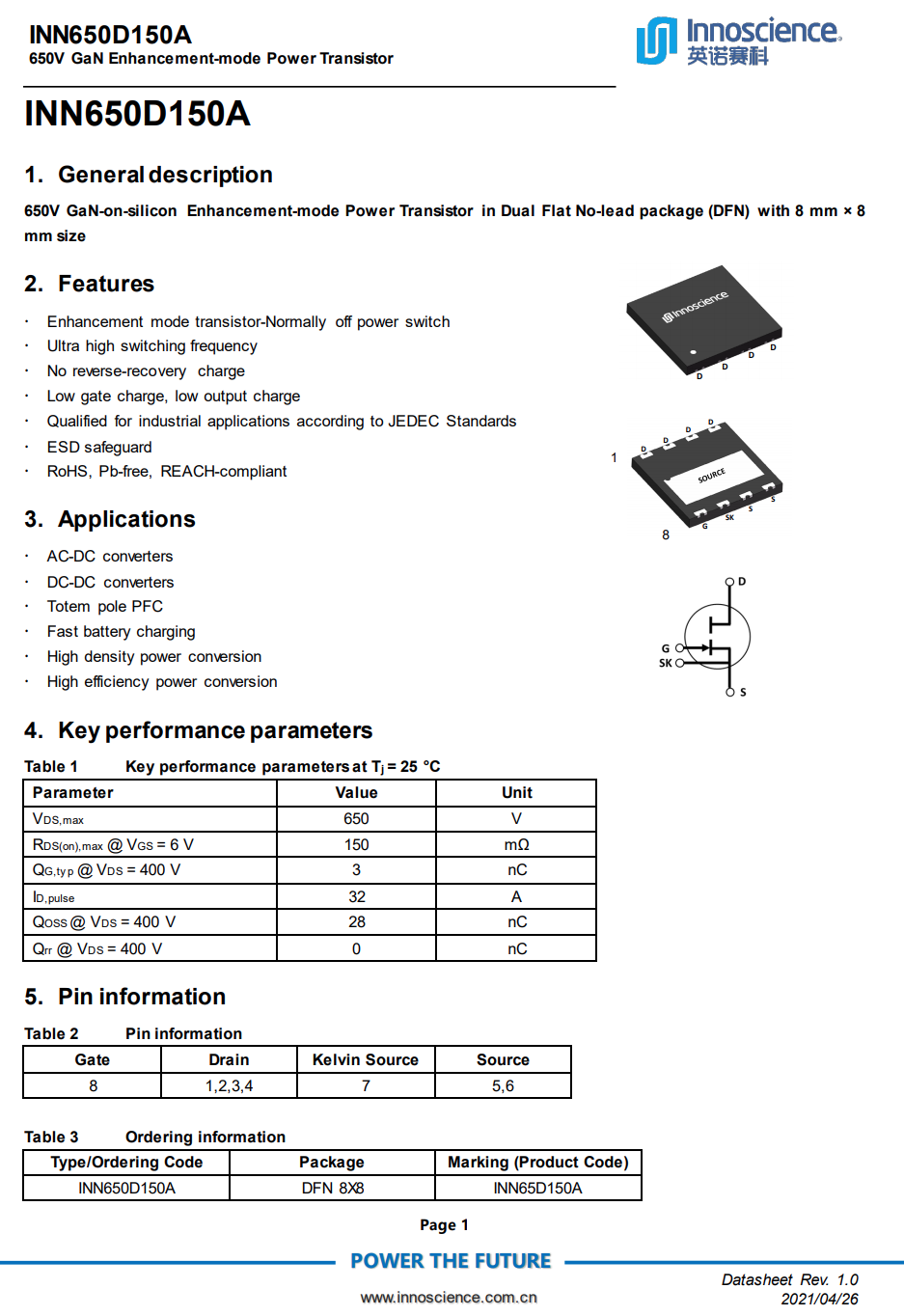
The INN650D150A supports AC-DC and DC-DC converter applications, including totem-pole PFC configurations, battery fast charging, as well as high power density and high-efficiency conversion applications.
Close-up of the PFC boost inductor.
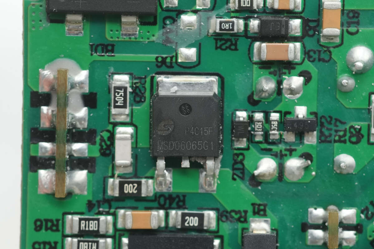
The PFC rectifier is from Msemitek, model MSD06065G1. It is a SiC diode rated for 650V and continuous forward current of 6A at 150°C, housed in a TO-252 package.
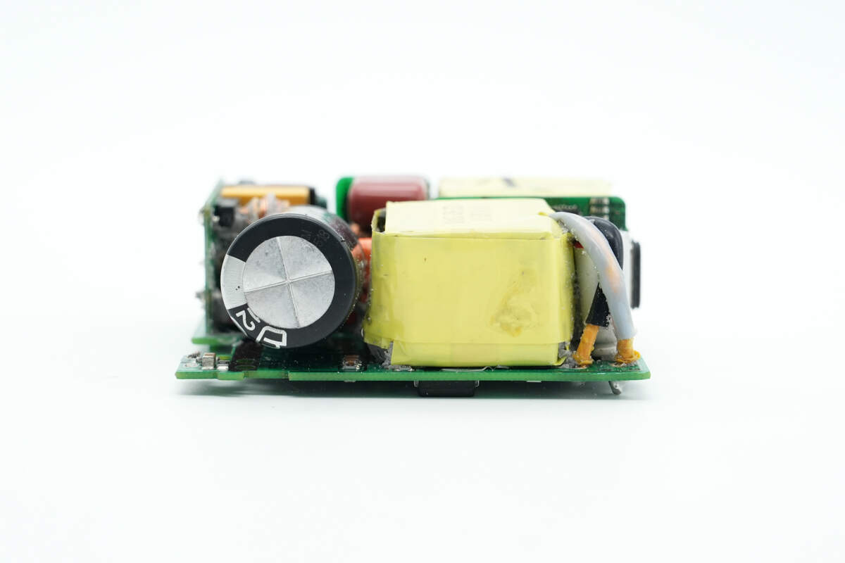
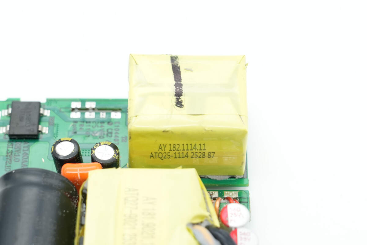
On the other side of the module, there is a high-voltage filtering electrolytic capacitor and a transformer.

The electrolytic capacitor is from ChengX, rated at 120μF, 420V.

The AHB controller is from JOULWATT, model JW1556. It is an asymmetric half-bridge flyback controller in a QFN 4x4-20 package, designed for offline flyback converter applications. It integrates an internal boost converter for power supply, supports an input voltage range of 2.5–38V, and operates at a maximum frequency of up to 1.5MHz, making it suitable for 65–300W fast charging applications.
Under heavy load, it operates in ZVS mode with Adaptive ZVS switching for optimized efficiency. At light loads, it switches to DCM operation. The controller provides dual output control for the main power switch and auxiliary switch, supporting high-voltage startup, X-capacitor discharge, burst mode control, and adjustable line compensation features.

Here is the information about JOULWATT JW1556.

The GaN half-bridge chip used is the JOULWATT JW1568K, which integrates a gate driver and two enhancement-mode GaN transistors, greatly simplifying the design and reducing system complexity. The integrated power GaN devices feature a 220mΩ on-resistance and a 650V voltage rating.
The JW1568K offers low quiescent current and supports a wide Vcc voltage range, ensuring precise matching of the internal high-side and low-side gate drivers, which helps improve system performance and stability. Its integrated high-side bootstrap circuit simplifies design and supports high-frequency operation up to 2MHz, delivering excellent performance in high-end applications.

Here is the information about JOULWATT JW1568K.
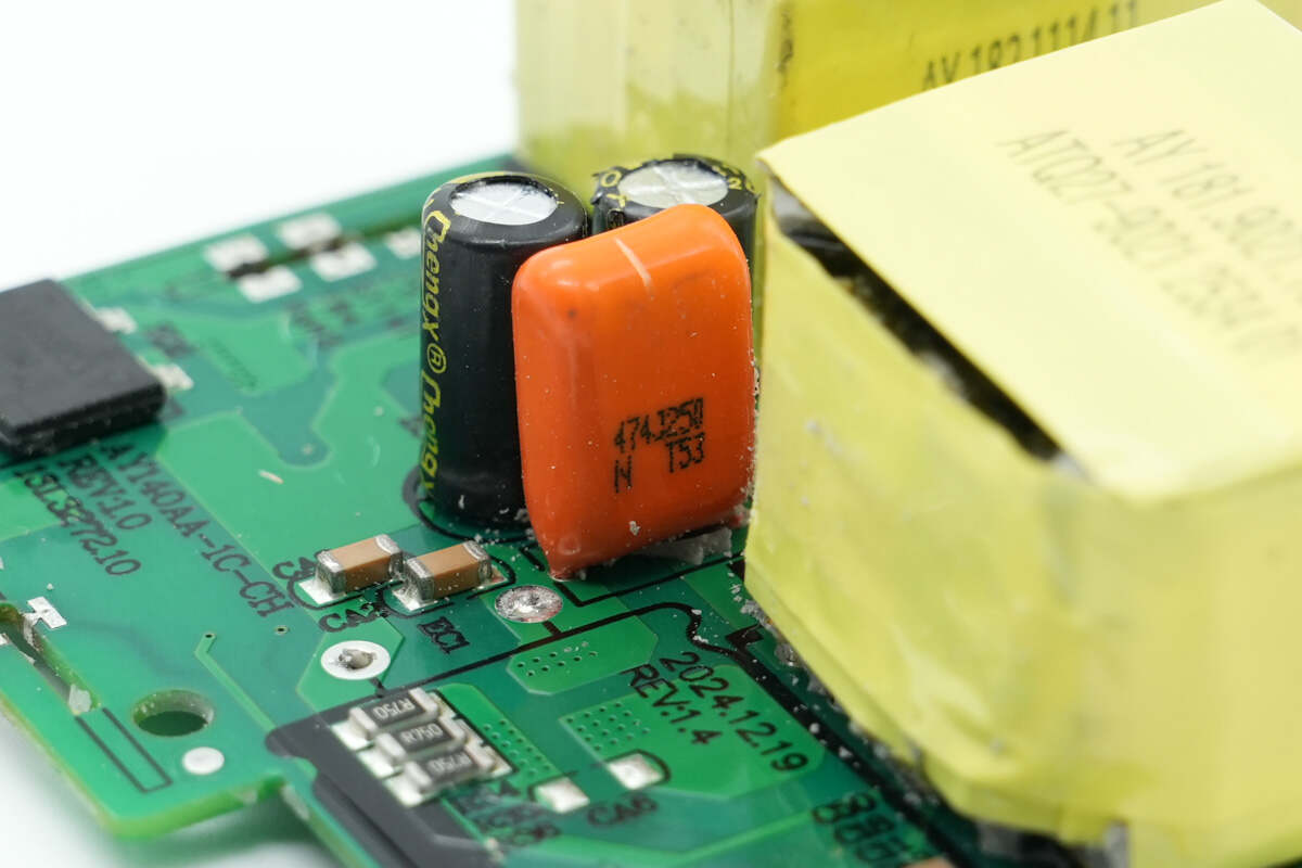
The resonant capacitor is rated at 0.47μF, 250V.

The two capacitors supplying power to the master control chip are also from ChengX, rated at 47μF 50V and 22μF 100V, respectively.
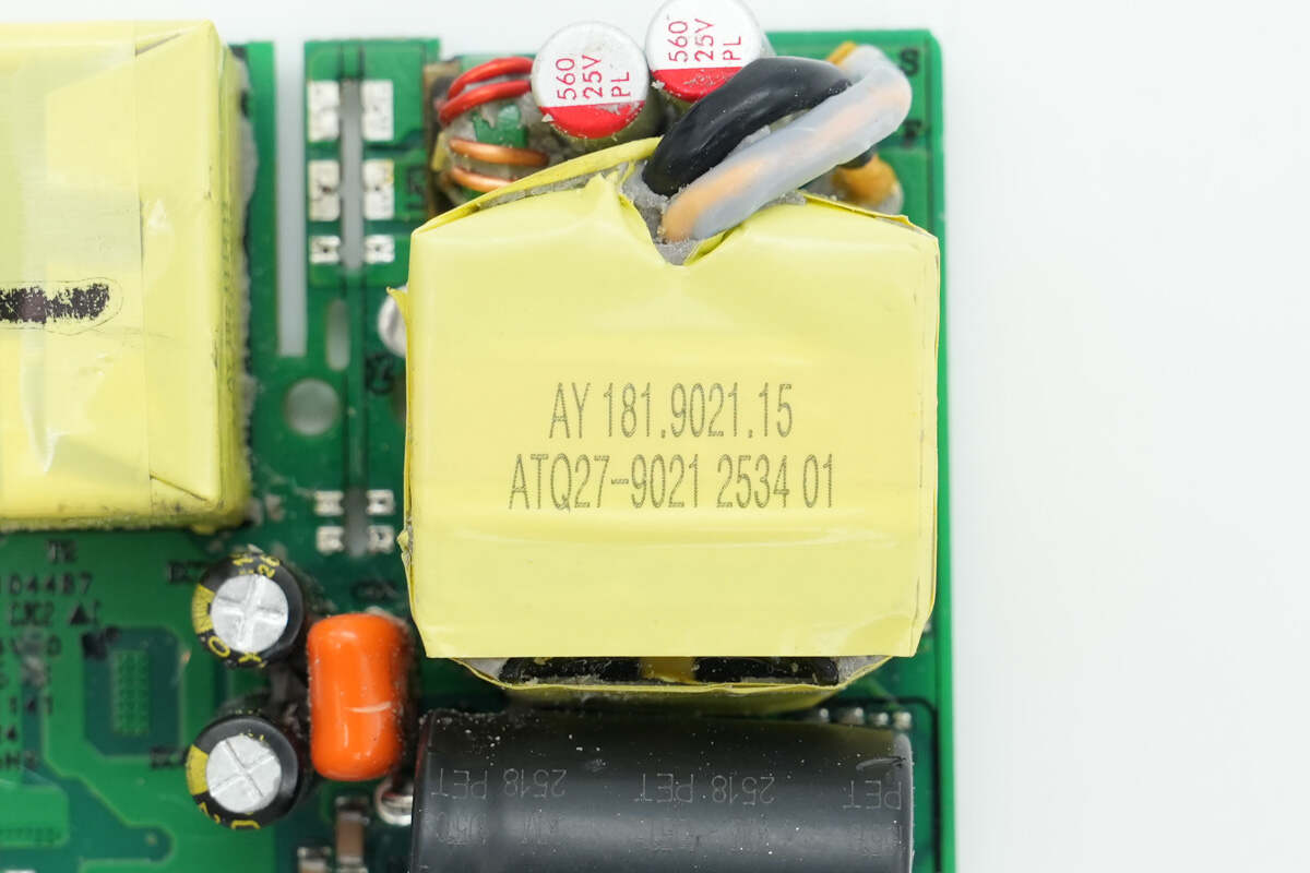
Close-up of the transformer.
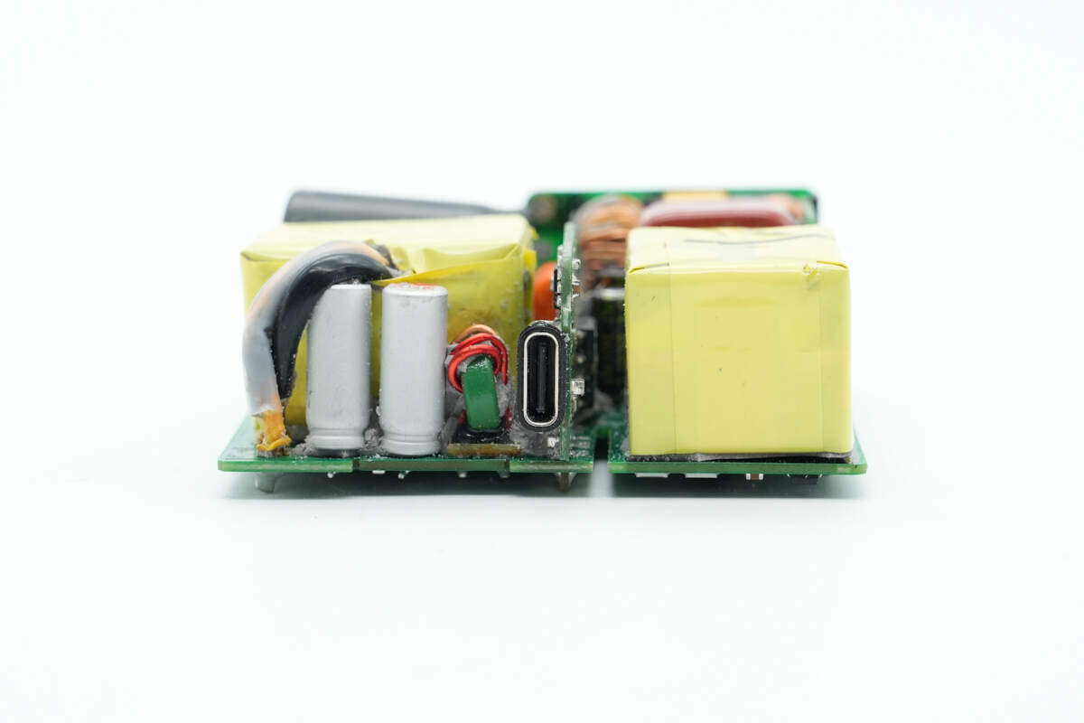
On the output side, the left contains a filter inductor and two solid capacitors for output filtering. The center houses the protocol PCB.
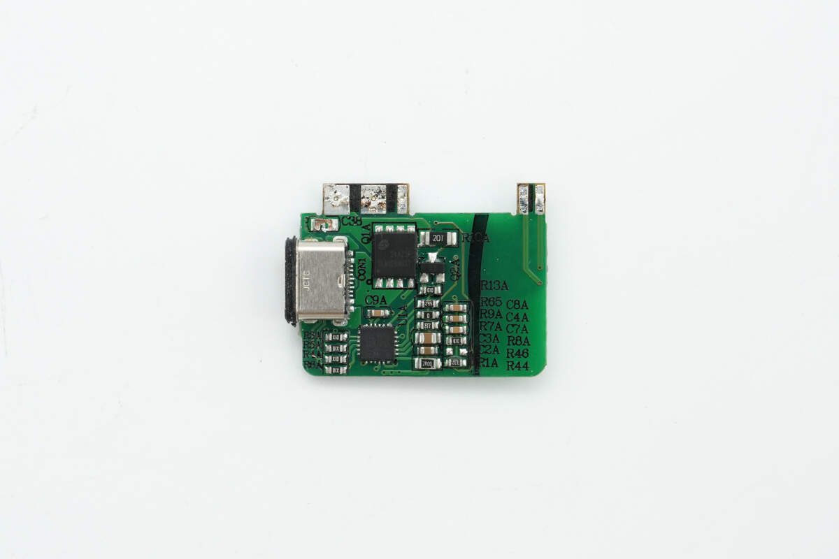
Remove the PCB with the USB-C socket. The front features the protocol chip and the output VBUS MOSFET.
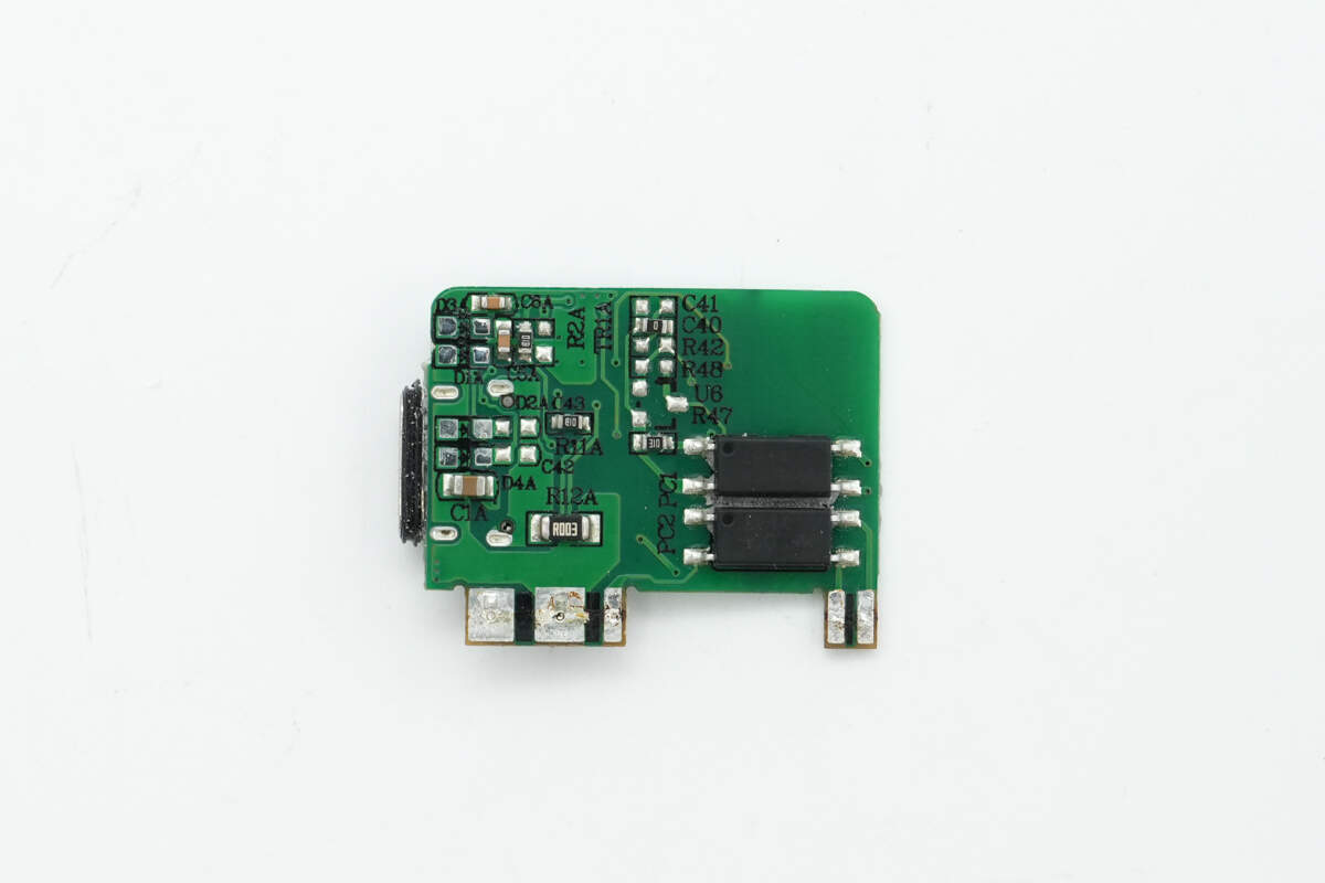
The other side is equipped with two optocouplers.

The two 1009 optocouplers are used for output voltage feedback and protection.

The SMD Y capacitors are from TRX. Their compact size and lightweight design make them well-suited for high-density power products such as GaN fast chargers. The model numbers are TMY1221K, TMY1102M, and TMY1681M.

The synchronous rectifier controller is from JOULWATT, marked with "JWRU", model JW7726H. It supports ACF, AHB, DCM, QR, and CCM flyback operating modes, and is compatible with both high-side and low-side configurations. It can be powered directly from the output voltage, features ultra-low quiescent current, and provides fast gate driving capability for efficient operation in CCM mode.

Here is the information about JOULWATT JW7726H.

The synchronous rectifiers are from JJM, model JMSH1004BG. These are N-channel MOSFETs rated for 100V with an on-resistance of 3.3mΩ, housed in a PDFN5×6-8L package.
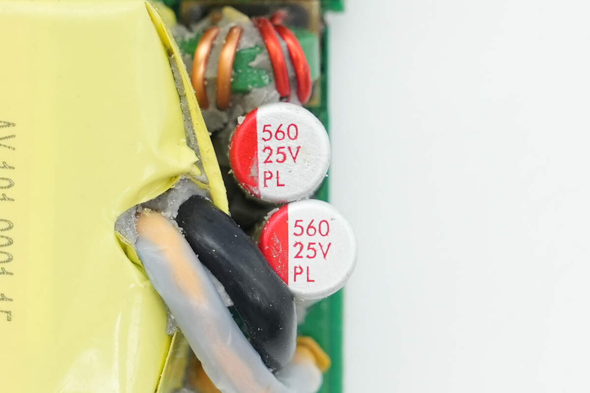
Both solid capacitors for output filtering are rated at 25V, 560μF.
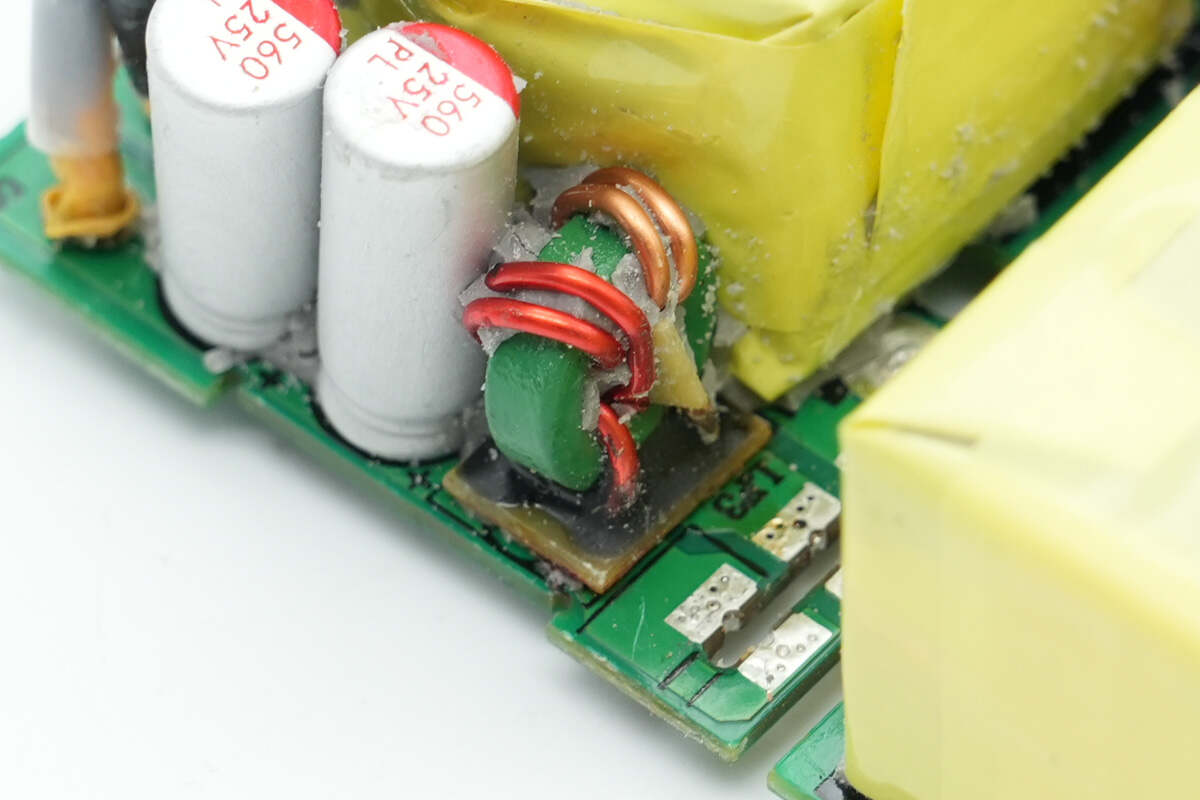
Close-up of filter inductor.

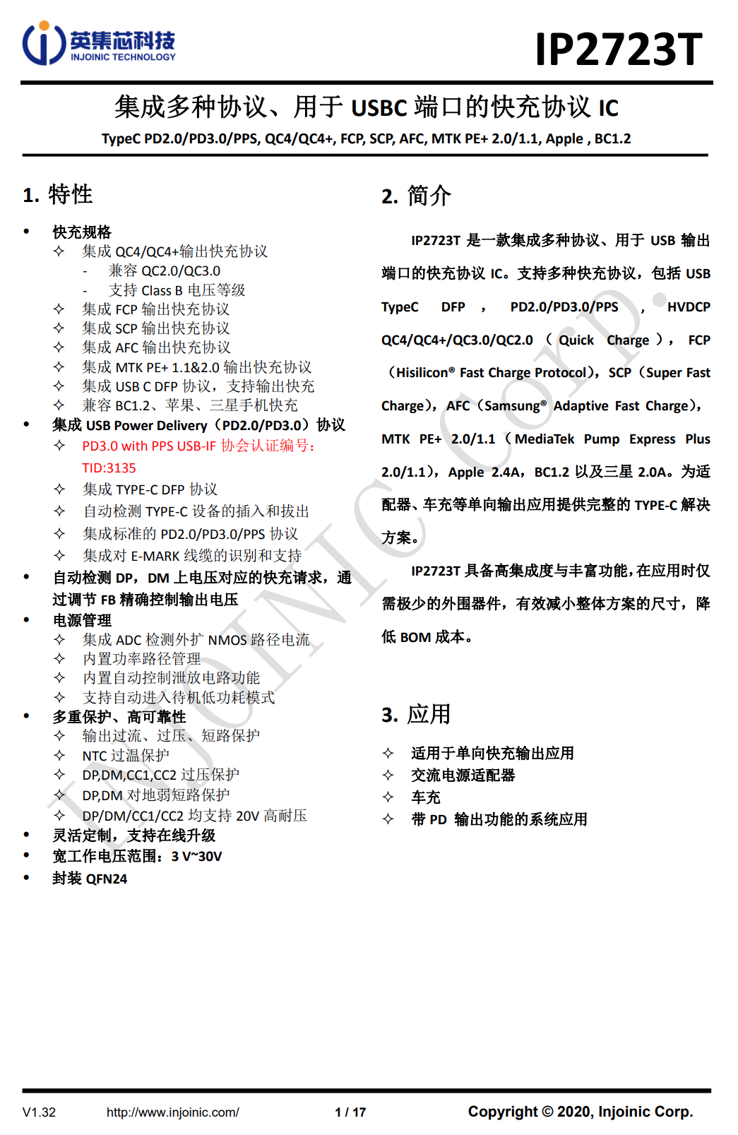
The protocol chip is from Injoinic, model IP2723T. It has passed USB-IF PD3.0 PPS certification, TID: 3135. It is a fast-charging protocol IC integrating multiple protocols for USB output ports. It supports various fast-charging protocols, including USB Type-C DFP, PD2.0/3.0, PPS, HVDCP, QC4, QC4+, QC3.0/2.0, FCP, SCP, AFC, MTK PE+ 2.0/1.1, Apple 2.4A, BC1.2, and Samsung 2.0A.
It provides a complete Type-C solution for unidirectional output applications such as adapters and car chargers. In addition, the IP2723T features high integration and rich functionality, requiring only a few peripheral components in practical applications, effectively reducing the overall solution size and BOM cost.
Here is the information about Injoinic IP2723T.

The output VBUS MOSFET is from Msemite, model SLM120N03T. It is an N-channel MOSFET rated for 30V with an on-resistance of 2.6mΩ, housed in a DFN5×6 package.
Well, those are all components of the MECHREVO 140W USB-C GaN Power Adapter.
Summary of ChargerLAB

Here is the component list of the MECHREVO 140W USB-C GaN Power Adapter for your convenience.
It supports a wide input voltage range of 100-240V and has passed CCC certification. It is equipped with a grounded plug for enhanced safety. It supports MECHREVO’s proprietary 140W PD fast charging protocol and comes with a 7A USB-C cable. It also supports 100W PD/PPS high-power fast charging, offering good performance and compatibility.
After taking it apart, we found that it is based on a PFC + AHB power architecture design, utilizing the complete JOULWATT power solution with JW1572, JW1556C, and JW7726HB, along with the JOULWATT JW1568K GaN half-bridge chip.
It uses a GaN component from Innoscience and SiC components from Msemite, with output controlled by the Injoinic IP2723T protocol chip. This integrated solution provides the product with high reliability and efficiency. The PCBA module is fully potted and covered with an integrated copper heatsink for thermal management, with well-executed insulation measures.
Related Articles:
1. Teardown of Meituan 7000mAh 22.5W Shared Power Bank (MT-D-7BDY0)
2. Teardown of GreatWall 550W 80 PLUS Platinum SiC Server Power Supply (GW-CRPS550)
3. Teardown of Belkin 15W Auto‑Tracking Stand Pro with DockKit (MMA008)