Introduction
Lenovo is aggressively expanding its accessory lineup alongside its core PC and mobile business. From power strips to high-capacity power banks, ChargerLAB has tracked Lenovo’s technical evolution through years of teardowns and lab testing.
The latest addition to the family is a sleek 68W GaN charger. Featuring a single USB-C port, it fully supports PD 3.0 and PPS protocols. It’s a versatile "one-charger-fits-all" solution, capable of juicing up everything from a high-end ThinkPad to a flagship smartphone at full speed.
Let's diving deep into the hardware to reveal the internal architecture and premium materials that power this new GaN unit.
Product Appearance
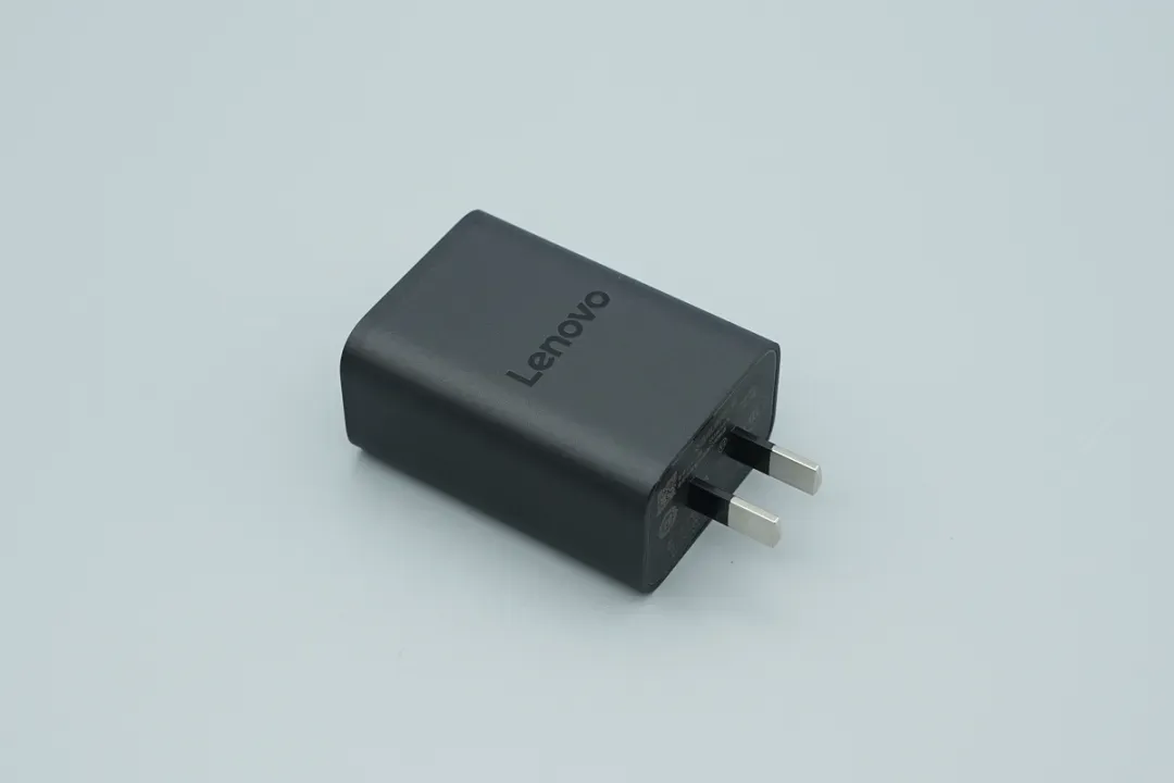
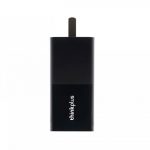
The Lenovo 68W USB-C PD Fast Charger features a sleek matte black finish and a clean, boxy aesthetic, complete with the Lenovo logo.
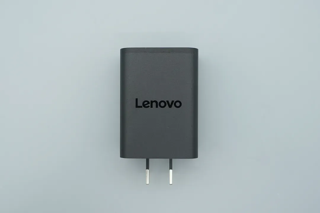
Featuring minimalist lines and subtly beveled corners, the chassis offers a refined feel that won't dig into your palms.
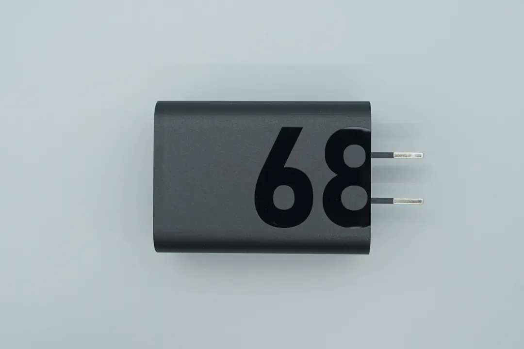
The bold '68' branding spans across the back, offering a strong sense of visual impact.
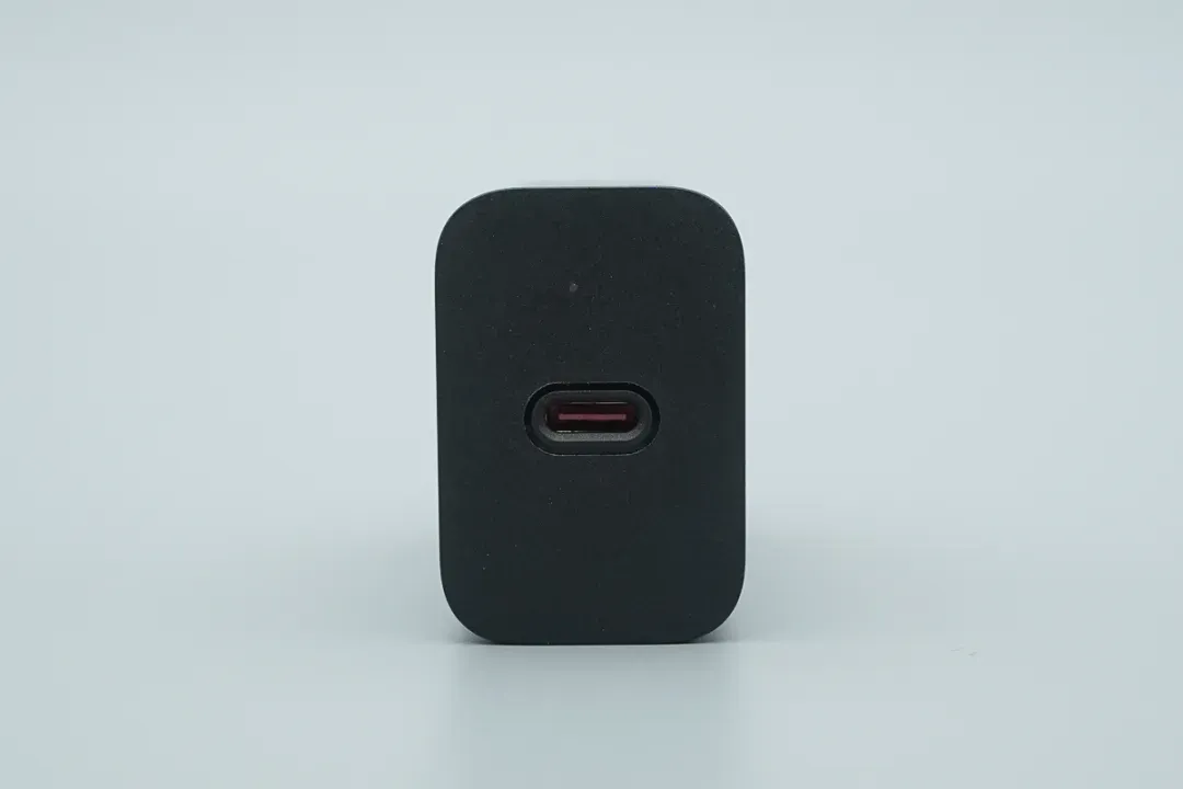
A single USB-C port sits right in the center of the output end, featuring a signature red interior that adds a pop of color.
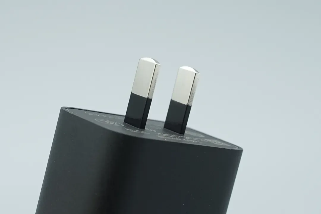
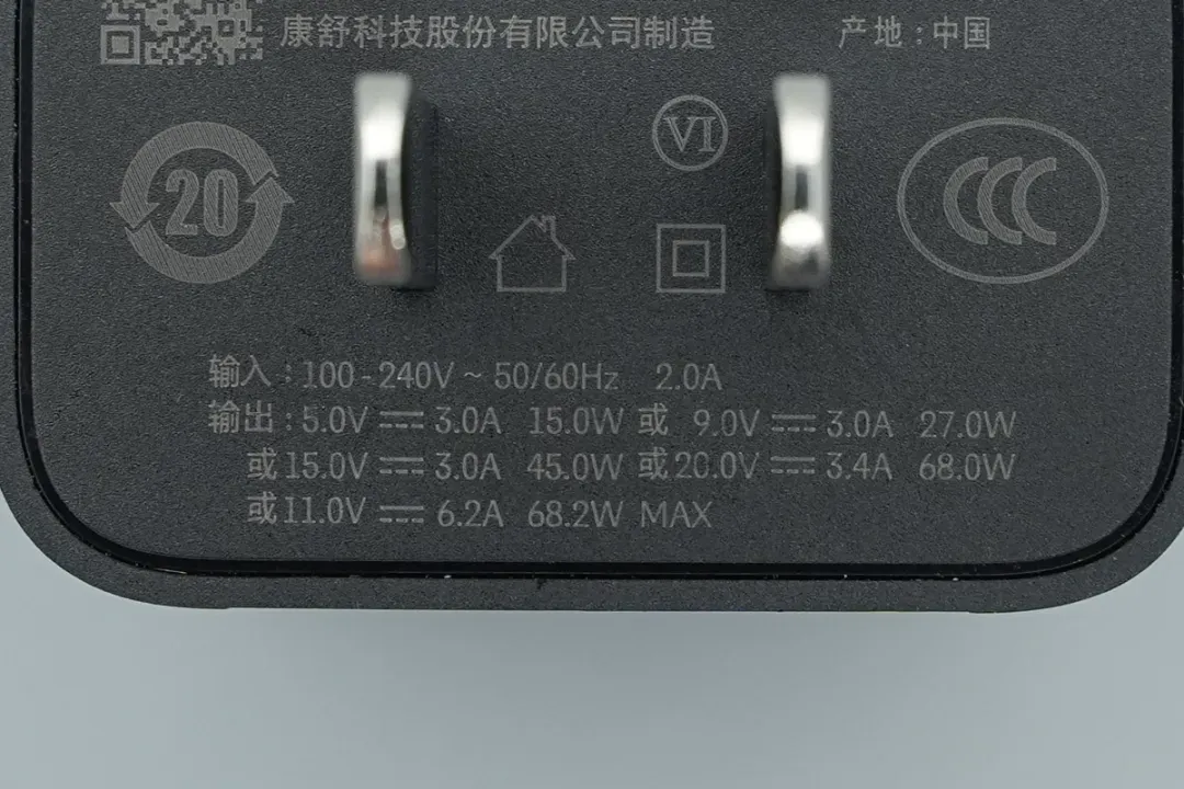
It features a fixed two-prong plug compliant with Chinese standards.
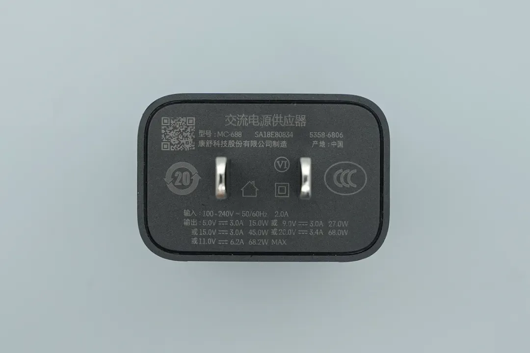
Detailed specs and regulatory icons are printed on the base for easy reference.
Product Specs (Model MC-688):
Input: 100-240V~ 50/60Hz 2.0A
Max Output: 5V3A, 9V3A, 15V3A, 20V3.4A and 11V6.2A (68.2W MAX)
Manufacturer: AcBel Polytech Inc.
Safety: CCC Certified.

The length of the charger is about 58.05 mm (2.285 inches).

The width of the charger is about 42.14 mm (1.659 inches).

The thickness of the charger is about 28.13 mm (1.107 inches).
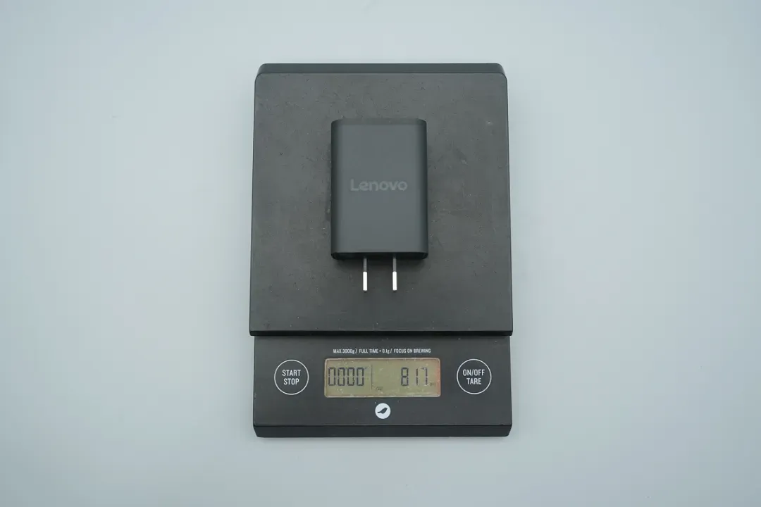
The weight is about 81.7 g (2.88 oz).
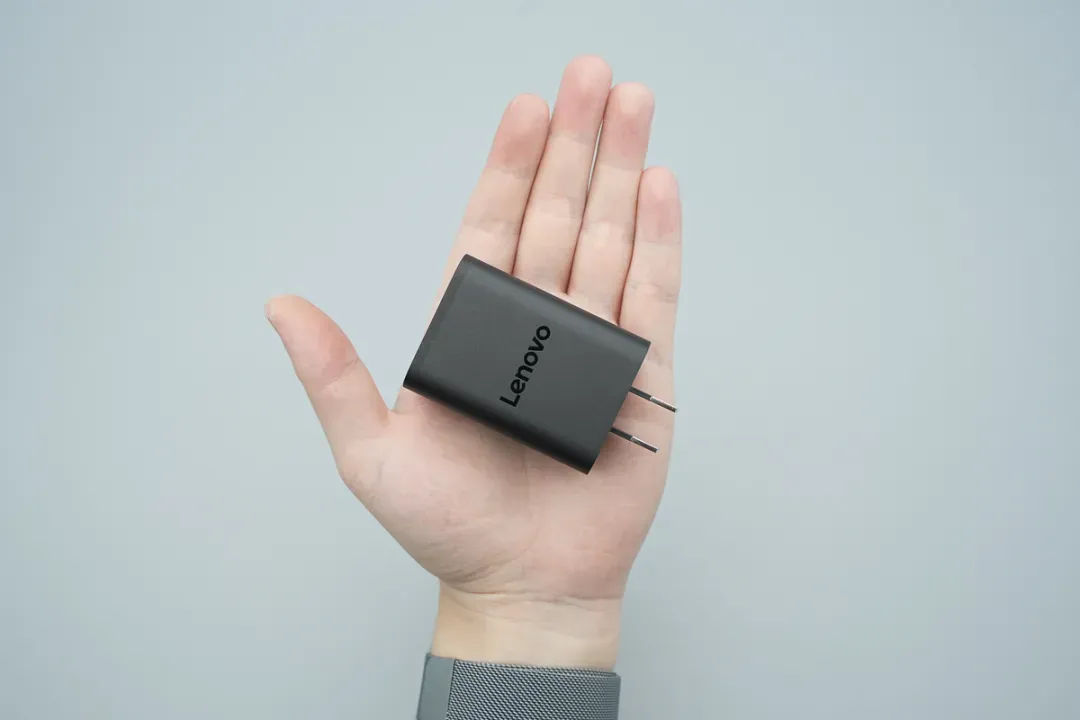
That's how big it is in the hand.
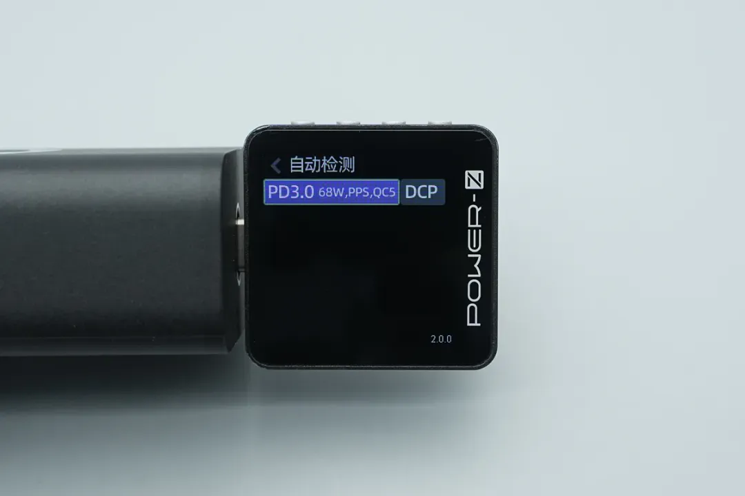
ChargerLAB POWER-Z KM003C shows that the USB-C port supports PD3.0/PPS, QC5, DCP.
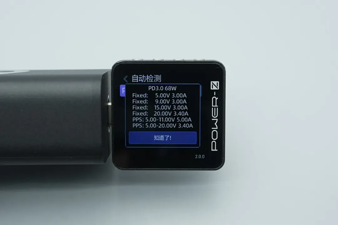
The PDO data reveals that the USB-C port features: 5V3A, 9V3A, 15V3A and 20V3.4A, features two PPS subsets: 5-11V5A and 5-20V3.4A.
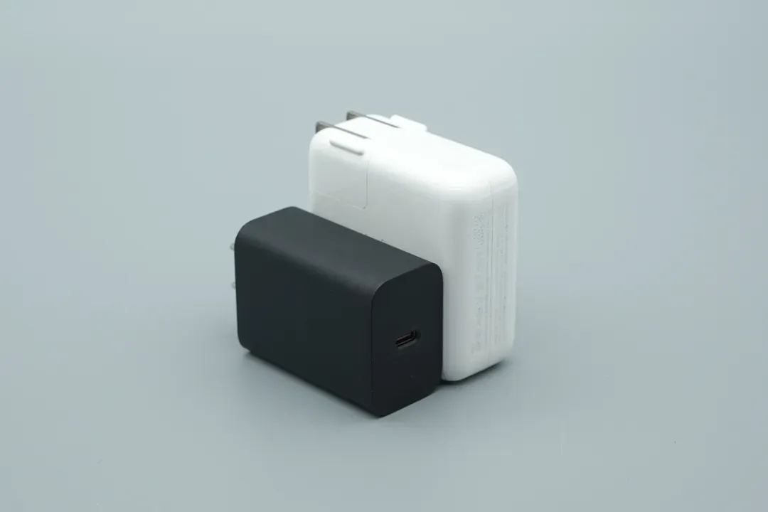
Put it with Apple’s 70W charger, it is noticeably smaller.
With the visual inspection and protocol testing complete, let’s move on to the detailed teardown.
Teardown
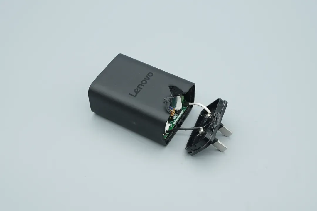
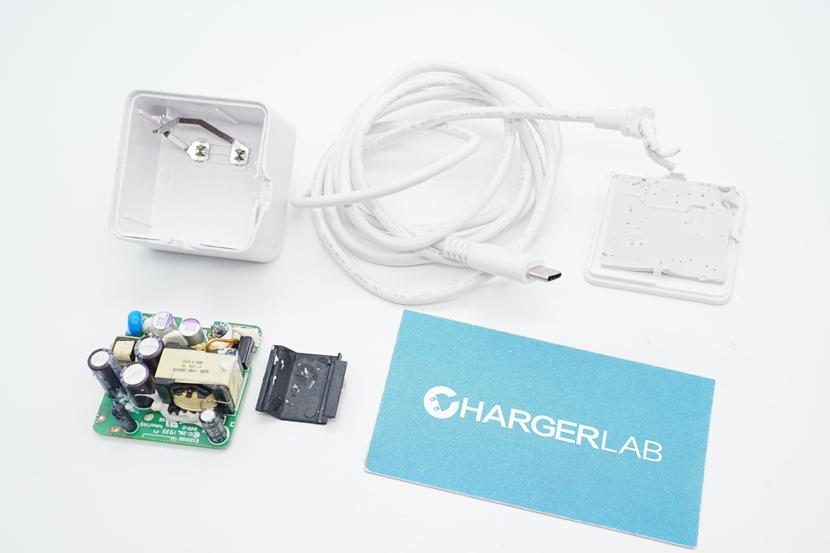
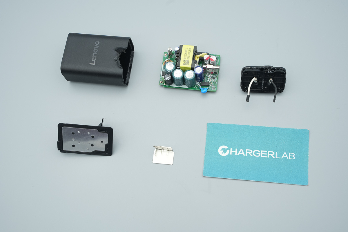
Prying open the casing along the seam reveals the interior is filled with white thermal potting compound, and the prongs are connected to the PCBA module via soldered lead wires.

The internal PCBA module is secured with white thermal potting compound, which serves multiple functions: electrical insulation, structural reinforcement of components, and enhanced thermal dissipation.
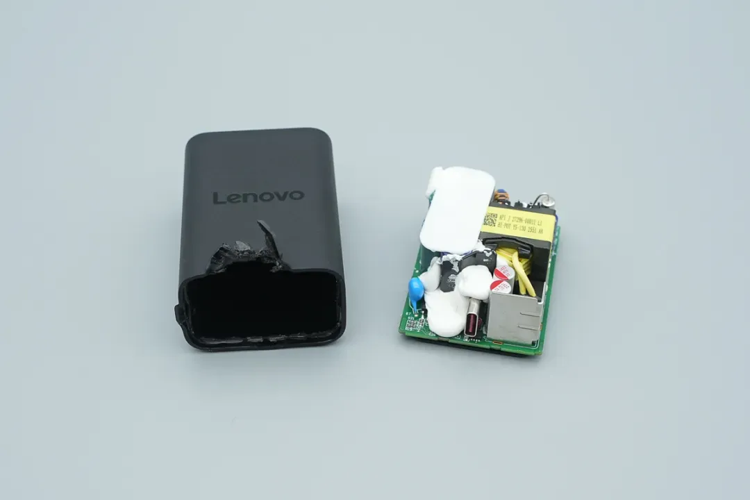
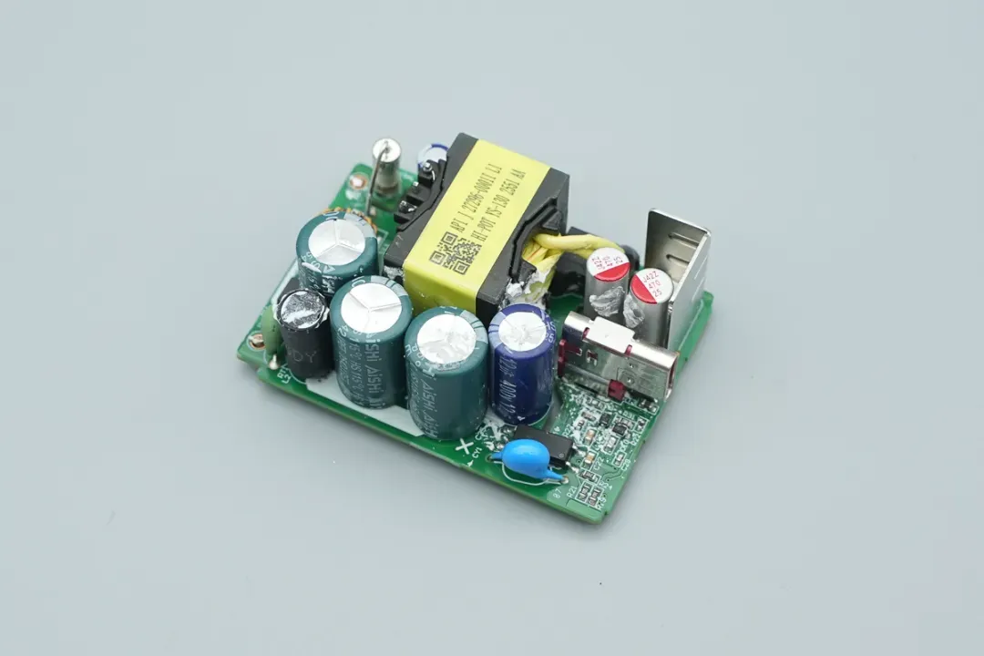
Removing the PCBA module from the black casing.
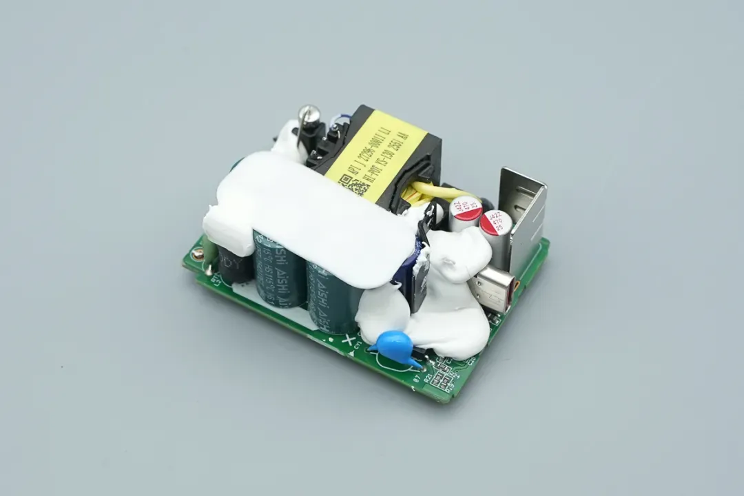
The PCBA module is densely filled with white thermal potting compound between components. Critical parts, including caps, chocks, and the transformer, are entirely encapsulated.
This structure enhances the overall structural integrity and help with cooling.
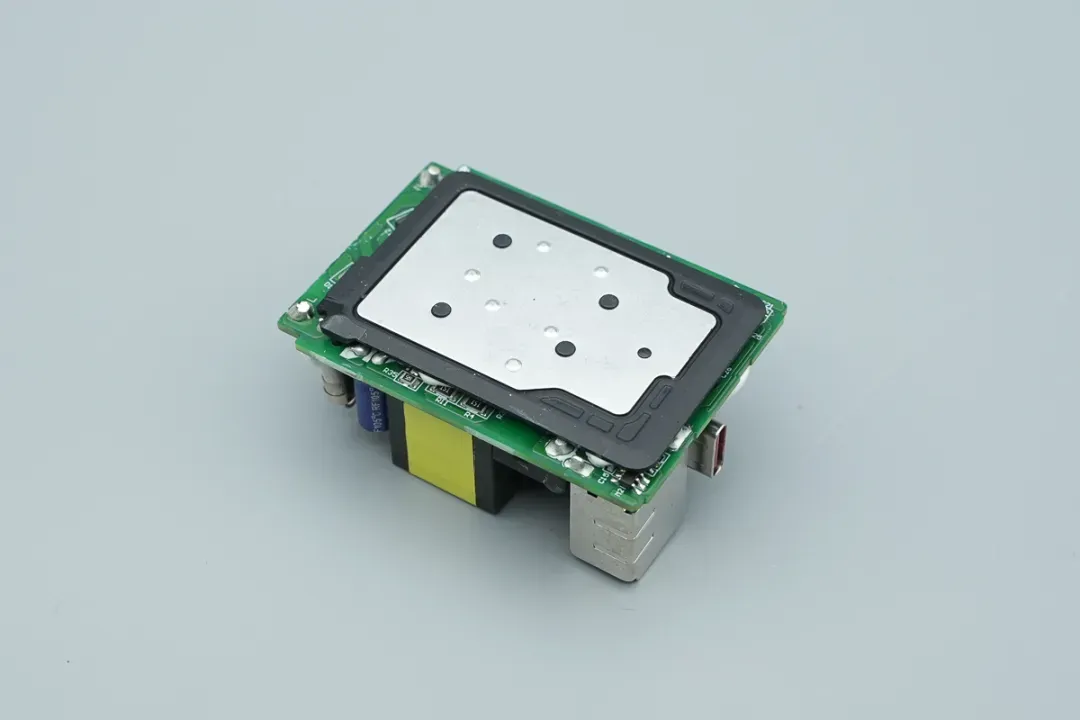
The back of the PCBA module is covered with a black insulation barrier and a metal heat spreader.

The length of PCBA is about 54.55 mm (2.148 inches).

The width of PCBA is about 38.01 mm (1.496 inches).

The thickness of PCBA is about 22.41 mm (0.882 inches).
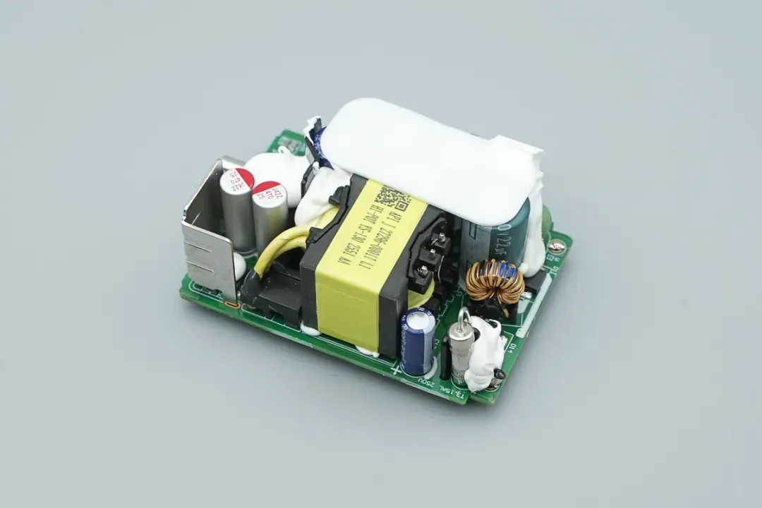
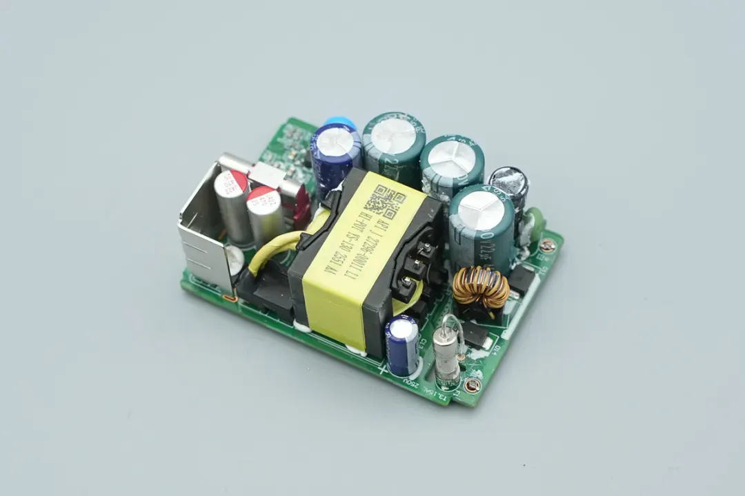
Removing the metal heat spreader and insulation barrier reveals white potting compound, applied to accelerate total system heat dissipation.
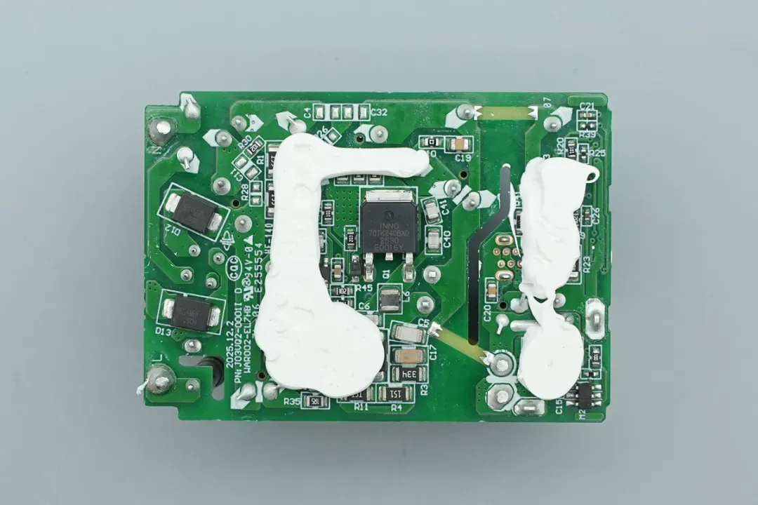
The overall view of the PCBA module after completely removing the white potting compound. It reveals the high-voltage filter caps, filter inductors, transformer, and output solid caps.
Another perspective of the PCBA reveals the input end features a time-delay fuse, a common-mode chock, and an NTC thermistor.
A full view of the PCBA's back side after cleaning off the white potting compound. The SMD components are arranged in a compact and orderly layout, with a clear isolation gap between the primary and secondary sides.
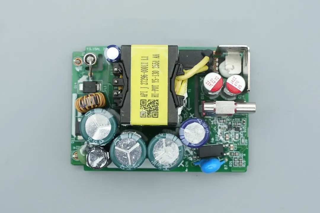
A top view of the PCBA module. Let’s dive into the front side first.
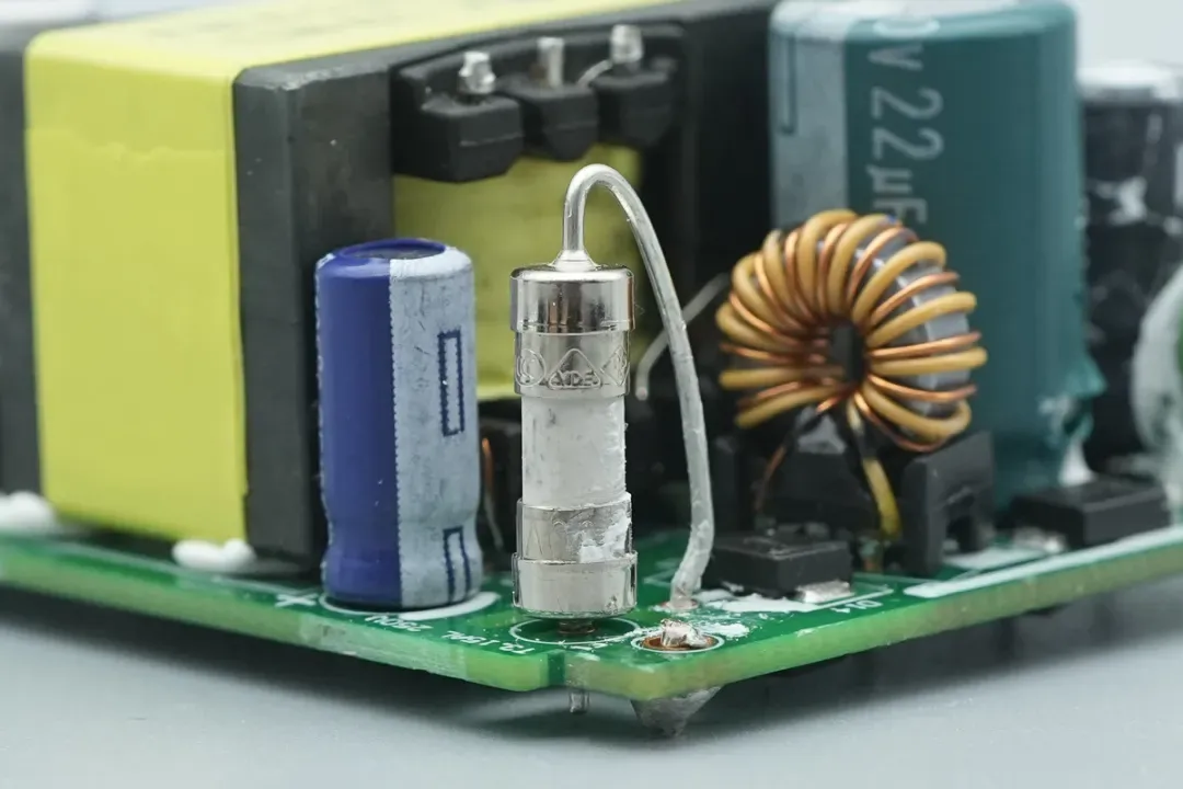
A close-up of the input end fuse.
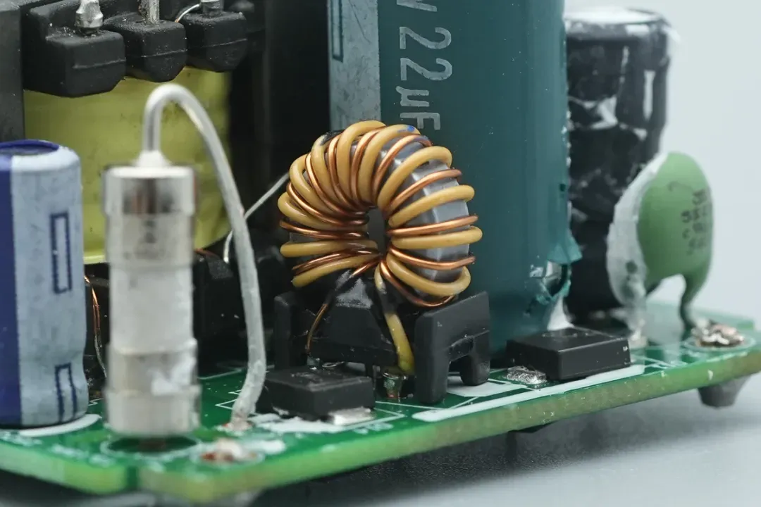
A common-mode chock.
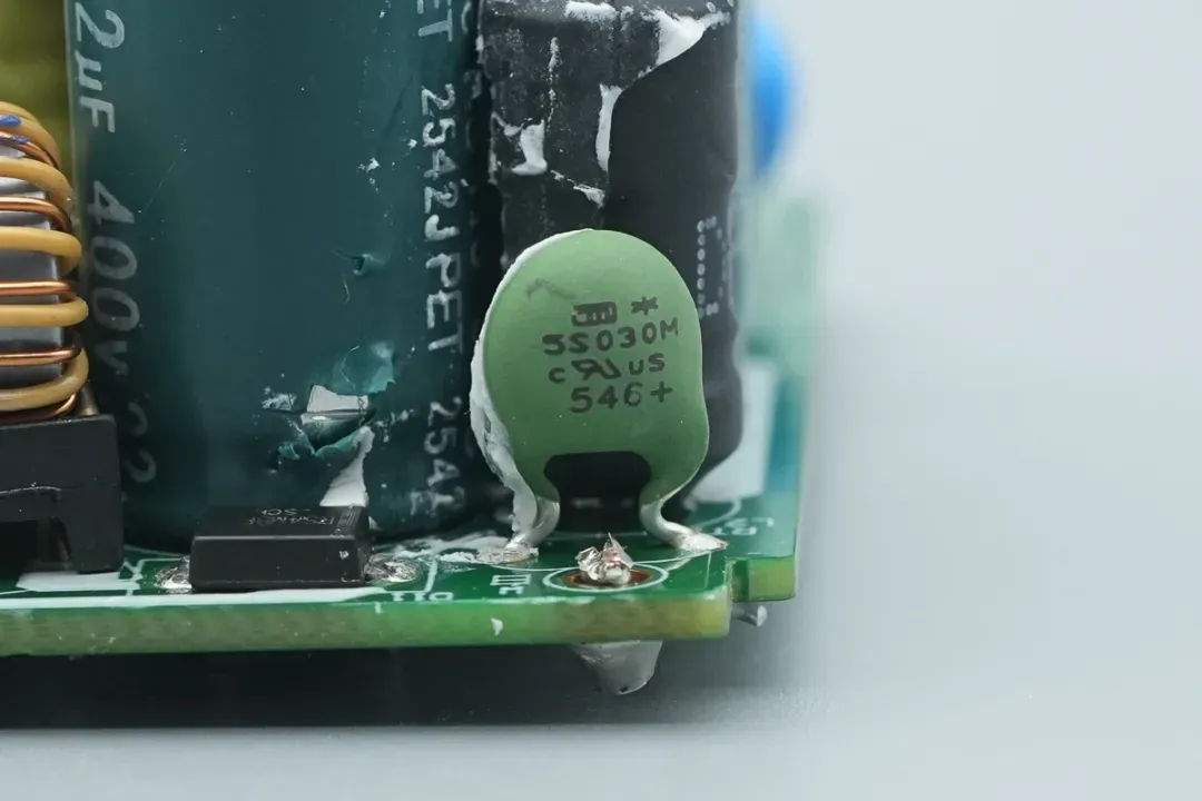
NTC Thermistor: Green, marked 5S030M.
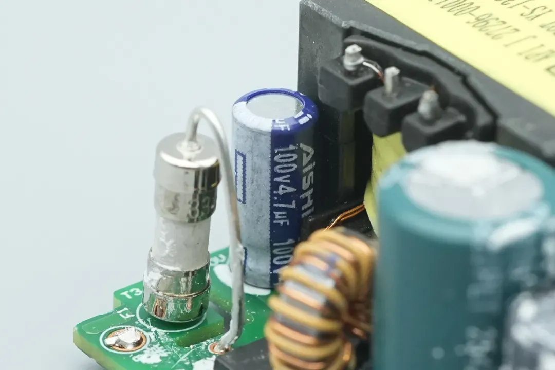
An AiSHi aluminum electrolytic cap, rated at 100V 4.7μF, provides filtered power supply for the primary master control chip.
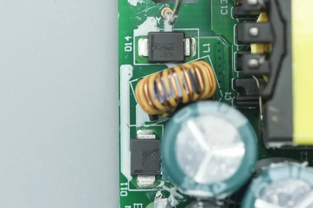
The RS4MBF SMD is utilized to form the rectifier bridge circuit.
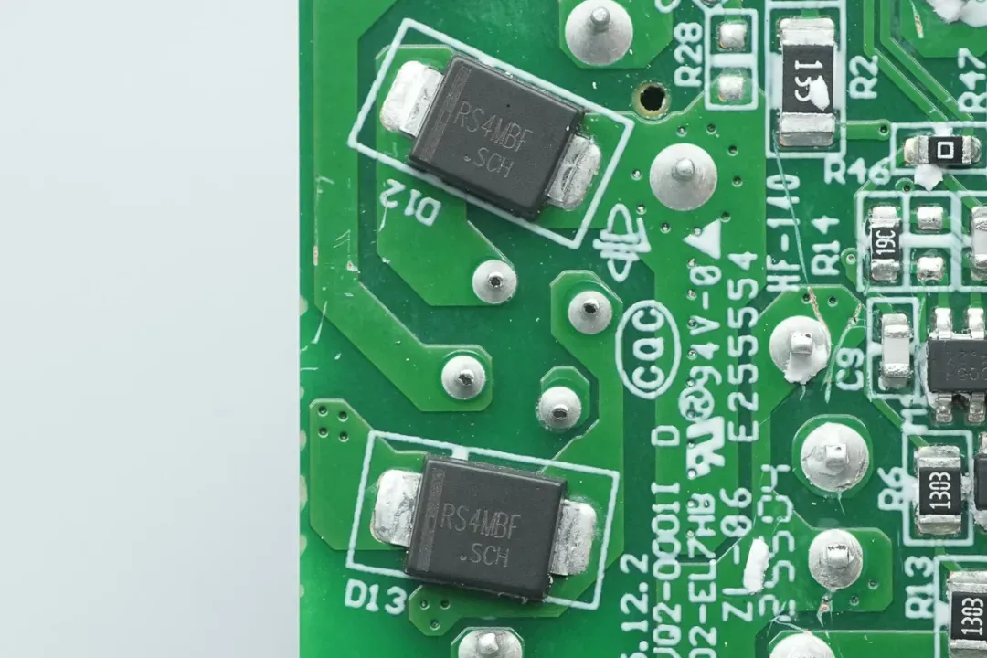
Two more RS4MBF diodes, part of the rectifier bridge.
Differential-mode inductor with black heat-shrink tube for insulation.
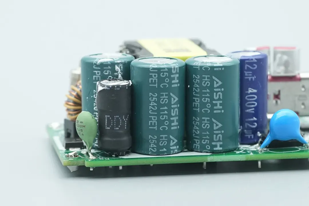
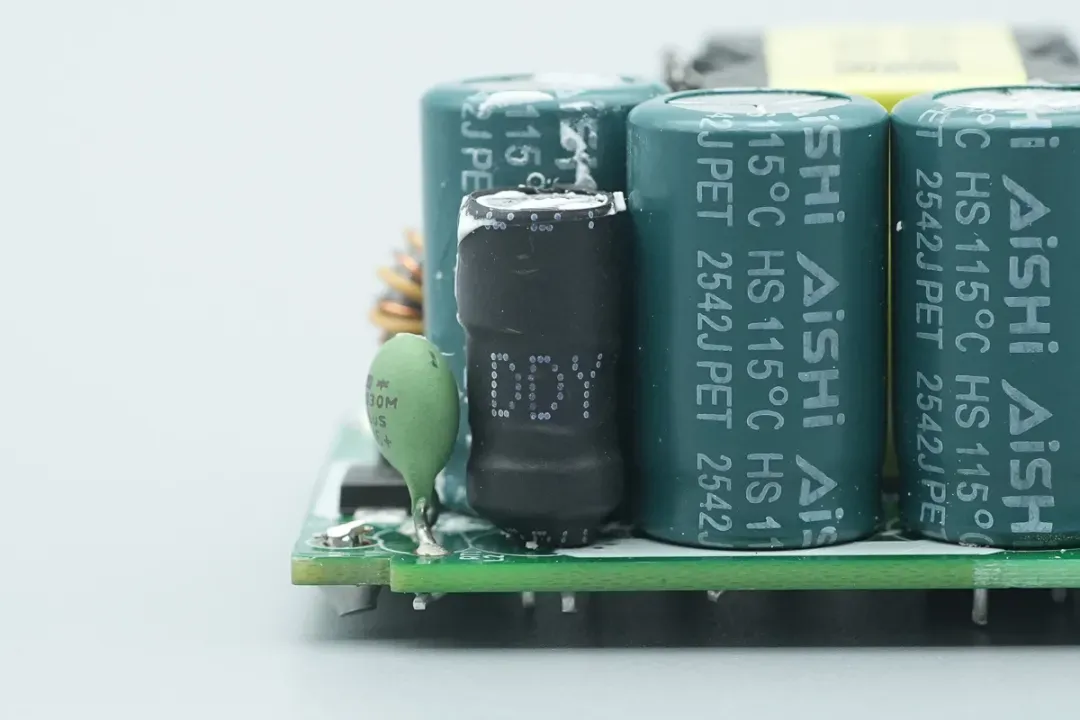
Three high-voltage filter caps are from AiSHi, 400V 22μF each.
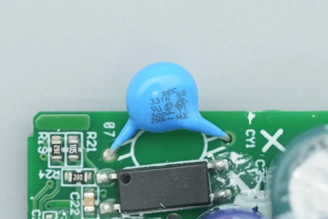
A blue Y-cap from STE is bridged between the primary and secondary sides, marked 331K.
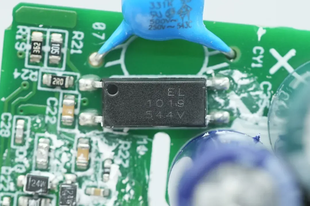
An optocoupler from Everlight, model EL1019.
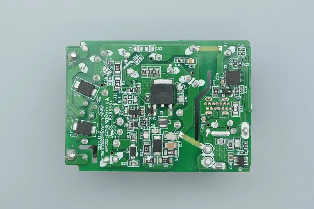
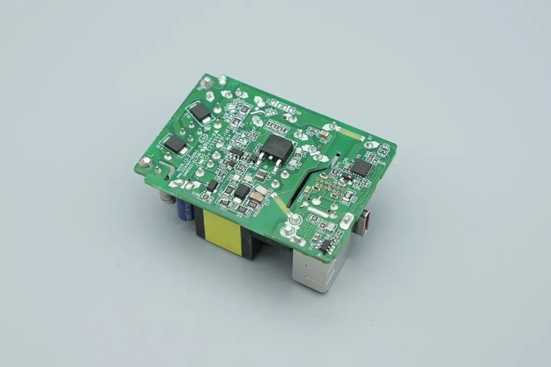
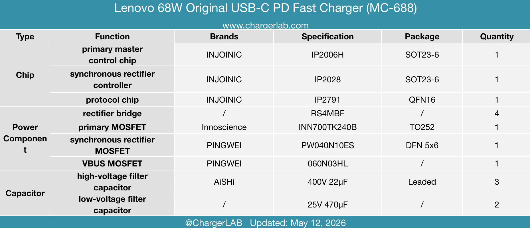
The bottom view of the PCBA module, featuring the primary controller, primary MOSFET, synchronous rectifier controller, and protocol chip.
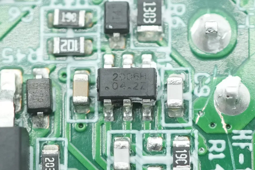
The primary master control chip is from Injoinic, model IP2006H, a high-performance multi-mode flyback controller. It features frequency foldback and valley switching technologies, while supporting adaptive switching frequency to enhance light-load efficiency. Its optimized maximum switching frequency helps reduce temperature rise and boost full-load efficiency.
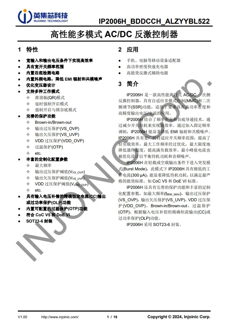
It also features Burst Mode to minimize standby power under light or no-load conditions, meeting CoC V5 and DoE Level VI standards. It integrates comprehensive protections, including Brown-in/Brown-out, output OVP/UVP, VDD OVP, input OVP and OTP. It also supports customizable parameters and OPP, all housed in a compact SOT23-6 package.
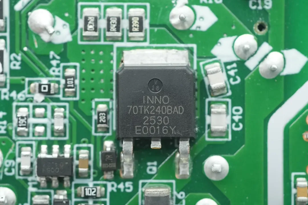
The primary GaN MOSFET is from Innoscience, model INN700TK240B, a 700V enhancement-mode GaN FET with a transient voltage rating of 800V and an on-resistance of 240mΩ. It meets JEDEC industrial standards, features integrated ESD protection, and is housed in a TO252 package.
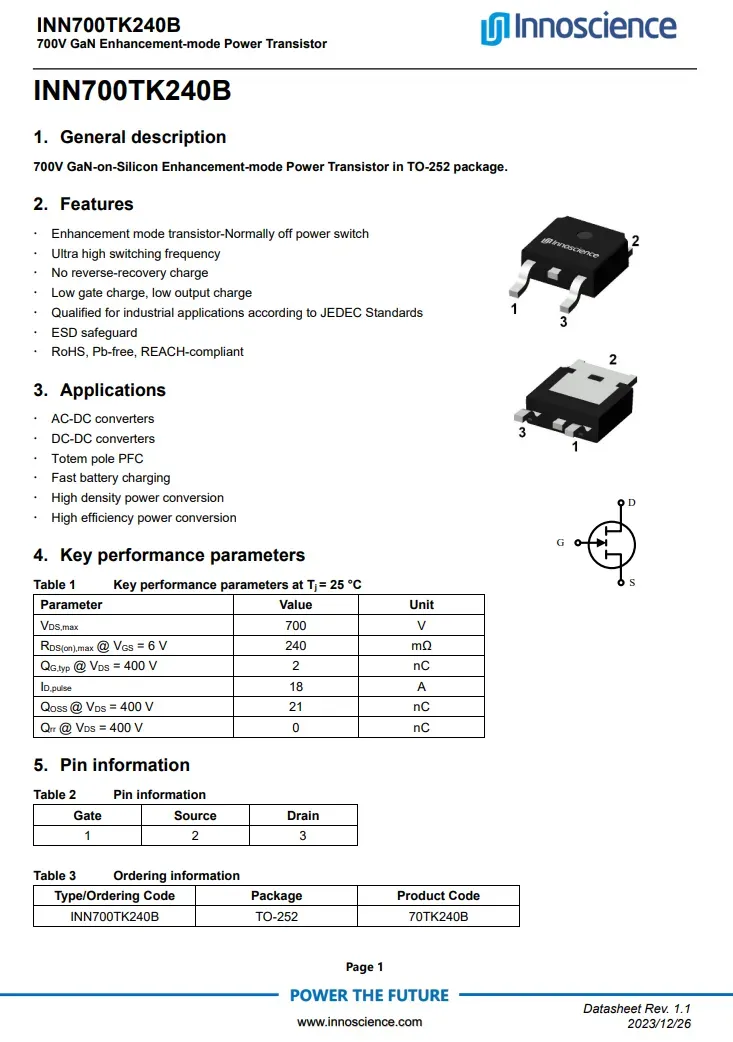
Here is the info about Innoscience, model INN700TK240B.
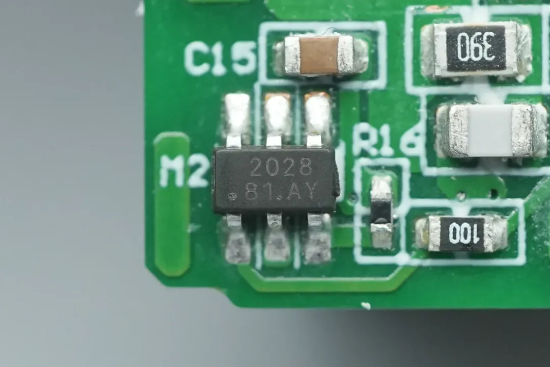
The synchronous rectifier controller is from Injoinic, model IP2028. It supports a wide output range from 3.3V to 28V (down to 0V).
With an integrated voltage regulator, it eliminates the need for auxiliary windings. It supports both high-side and low-side configurations and is fully compatible with CCM, DCM, QR, and ZVS operating modes.
It features Vds volt-second integration detection to prevent false triggering during DCM, QR ringing, or ZVS operations. Combined with a -30mV pre-turn-off threshold and a 30ns switching delay, it ensures rapid and precise MOSFET shutdown.
With a standby current as low as 30μA and a minimalist peripheral circuit in an SOT23-6 package, it is ideal for high-power density fast-charging designs.
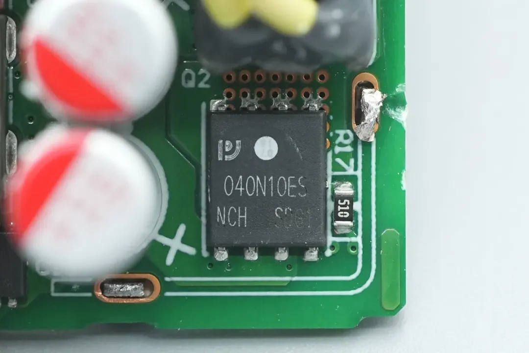
The synchronous rectifier MOSFET is from PINGWEI, model PW040N10ES, an NMOS with a 100V voltage rating and an ultra-low on-resistance of 3.4mΩ. It is housed in a DFN5x6 package.
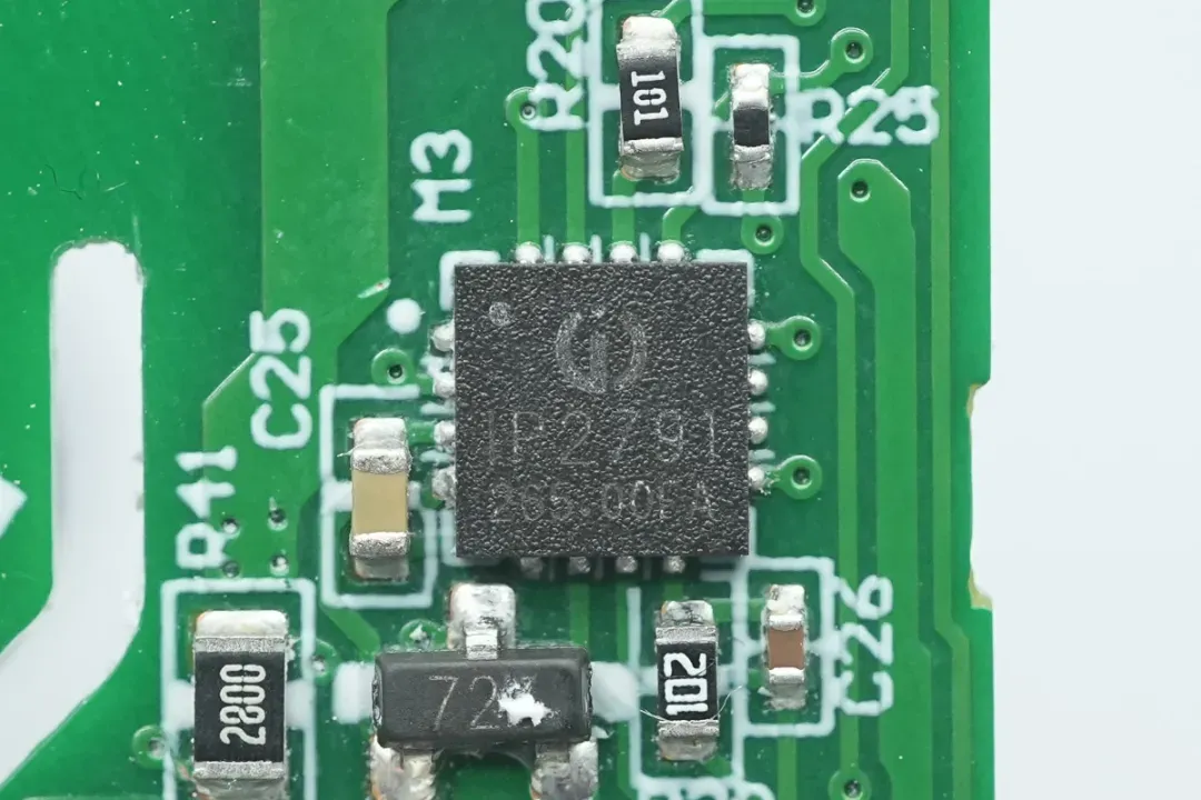
The protocol chip is from Injoinic, model IP2791, a highly integrated fast charge protocol IC designed for USB Type-C output. It supports USB Type-C DFP, PD2.0/PD3.1/PPS, QC3.0/QC2.0 and BC1.2, providing a comprehensive Type-C solution for adapters and car chargers.
IP2791具备高集成度与丰富功能,在应用时仅需极少的外围器件,有效减小整体方案的尺寸,降低BOM成本。
It features a high integration, requiring minimal peripheral components in application. This effectively reduces the overall size and lowers the BOM.
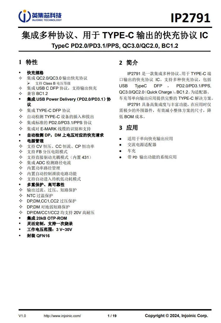
The VBUS MOSFET for the USB-C port is from PINGWEI, marked 060N03HL.
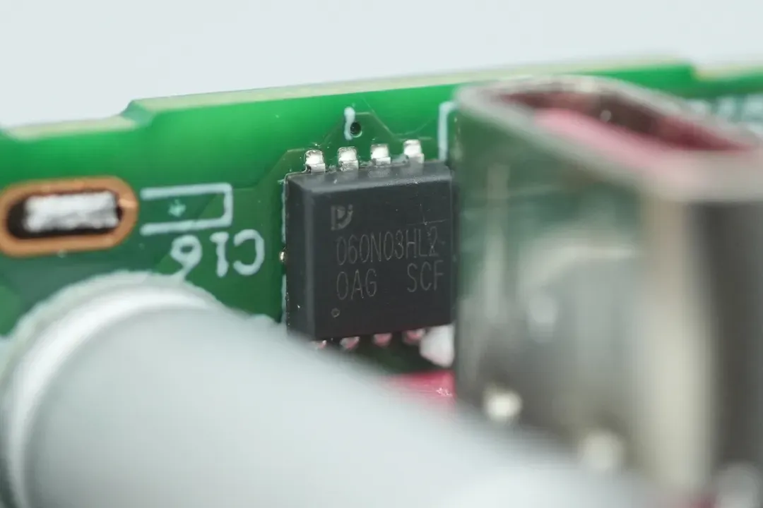
A close-up of the two output filter solid caps, each with a specification of 25V 470μF.
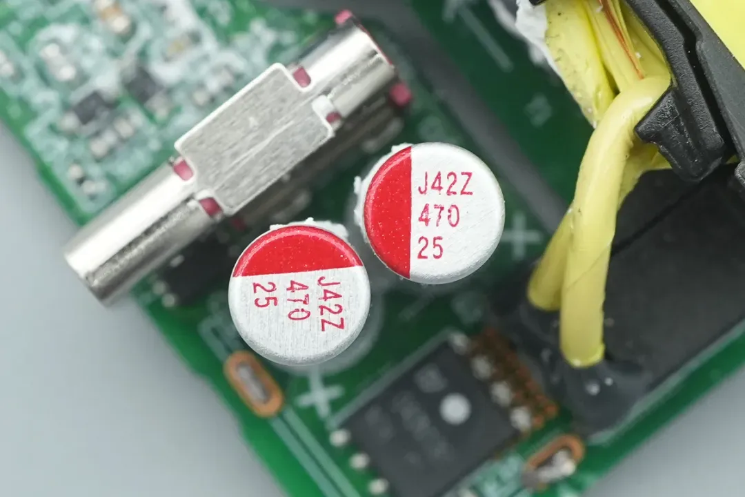
A close-up of the transformer, featuring an info label, model API J 27296-00011 L1 HI-POT YS-130.
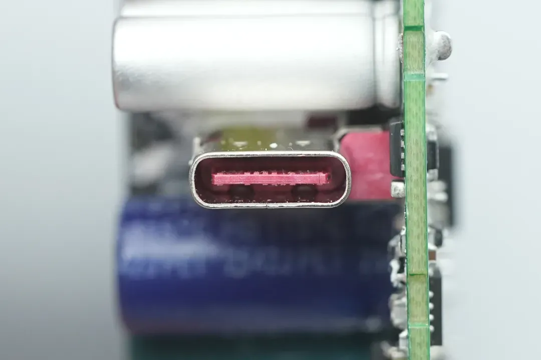
A close-up of the USB-C female connector, featuring a distinctive red plastic sheet.
Well, those are all components of the Lenovo New 68W GaN Charger.
Summary of ChargerLAB
Lenovo's 68W GaN charger maintains its signature family design language, featuring a matte black chassis paired with a glossy logo, making it highly recognizable. Supporting PD/PPS protocols, it delivers an optimized charging experience whether powering Lenovo’s ultra-slim laptops or providing fast charging for smartphones.
We learn that the unit is manufactured by AcBel. The internal design utilizes a potting compound process for enhanced durability. The PCBA module is fully coated with thermal conductive silicone on both sides and is equipped with a large-area metal heat sink and insulating shields on the rear, demonstrating superior craftsmanship.
The charger utilizes a highly integrated all-in-one Injoinic solution. The primary controller, synchronous rectification (SR) controller, and protocol chip are the Injoinic IP2006H, IP2028, and IP2791 respectively. This one-stop solution ensures exceptional system synergy.
The primary power semiconductor is the Innoscience INN700TK240B GaN FET, while the secondary-side SR MOSFET and VBUS MOSFET are both sourced from PINGWEI. The high-voltage filter caps are from AiSHi. Overall, this charger is a robustly engineered OEM fast-charging product featuring premium component selection and solid build quality.
Related Articles:
1. Dual-Standard Drafter: Lenovo Sets New Rules for PD 3.2 Fast Charging
2. Teardown of Lenovo thinkplus 240W Qlex Dual USB-C Retractable Cable (CBQX240A)
3. Compatibility Test of Lenovo Legion Go S