Introduction
We got our hands on the original Lenovo 100W GaN power adapter for laptops. It features a GaN-based design, with compact dimensions of 62.5 x 62.5 x 32.5mm and a lightweight of only 238g. It also includes a 1.8-meter USB-C cable, making it convenient and portable. Let’s take it apart and examine its design in detail.
Product Appearance

The adapter is white.

The front diagonal features the Lenovo logo and "100W" branding.
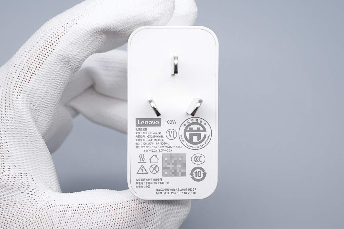
The input side of the casing has the printed specifications.
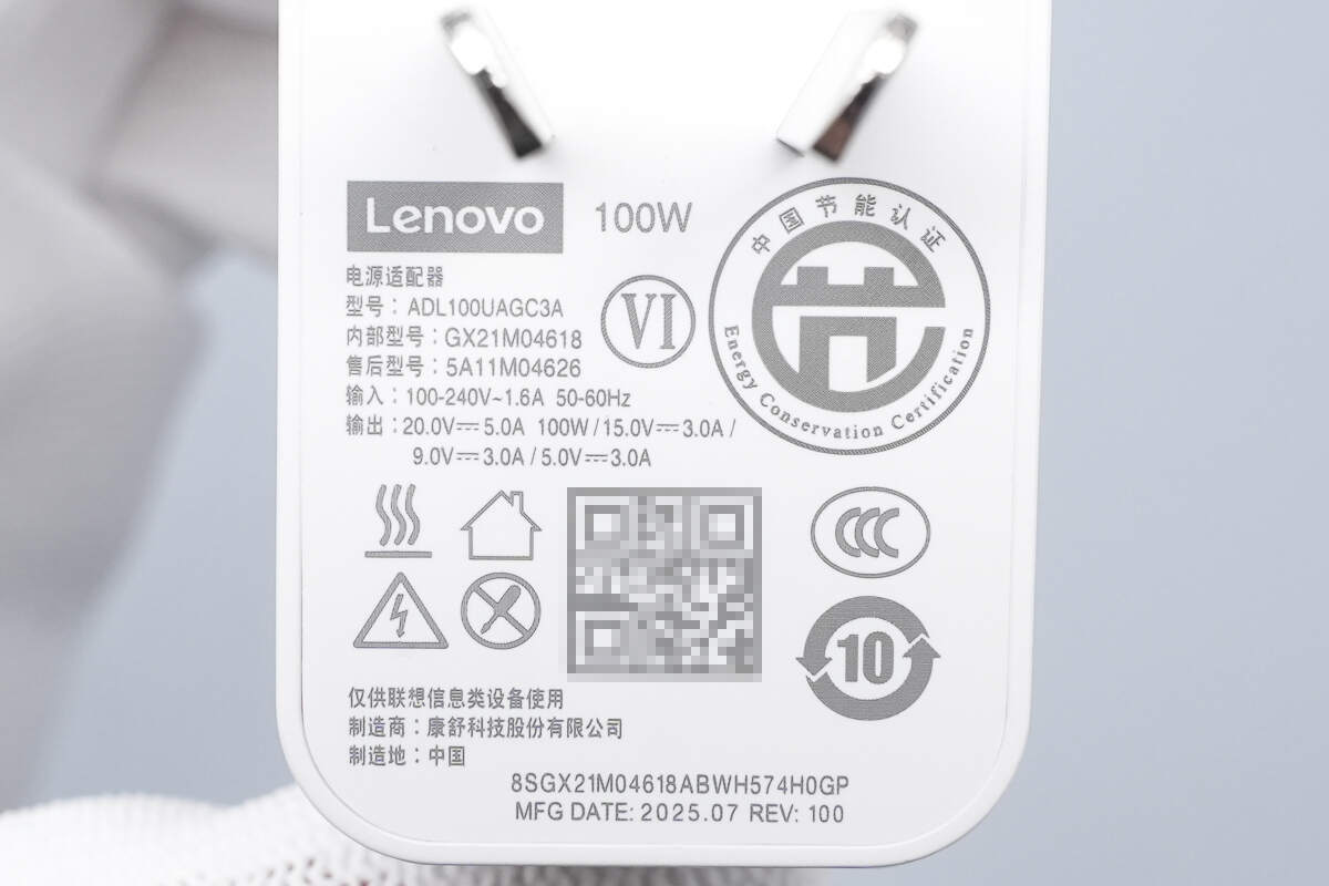
Model: ADL100UAGC3A
Input: 100-240V~50/60Hz 1.6A
Output: 5V3A, 9V3A, 15V3A, 20V5A
The product has passed CCC certification, VI-level energy efficiency certification, and China Energy Conservation certification.
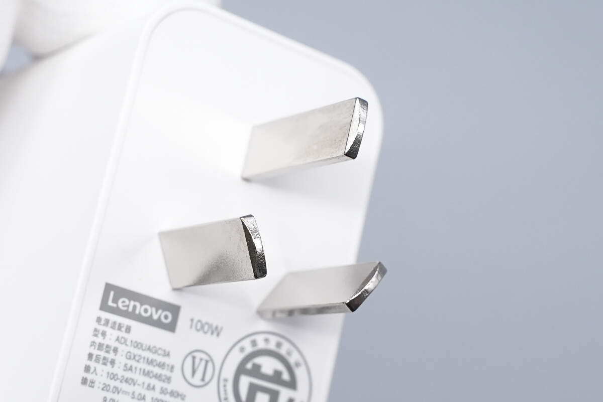
It is equipped with a three-prong plug.

The output cable connection to the body features a groove for protection.
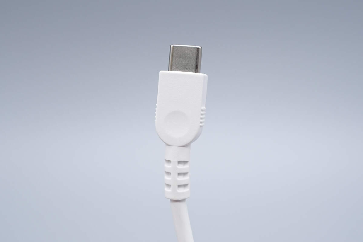
The USB-C connector has a matte-finish casing.
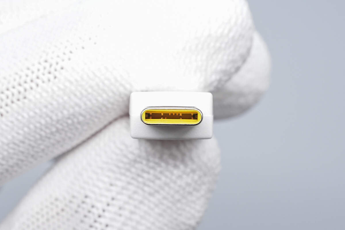
The USB-C connector features a non-full PIN design.

The length of the adapter is about 62.46 mm (2.46 inches).

The width is about 62.47 mm (2.46 inches).

The thickness is about 32.53 mm (1.28 inches).

The length of the output cable is about 180 cm (70.87 inches).

That's how big it is in the hand.
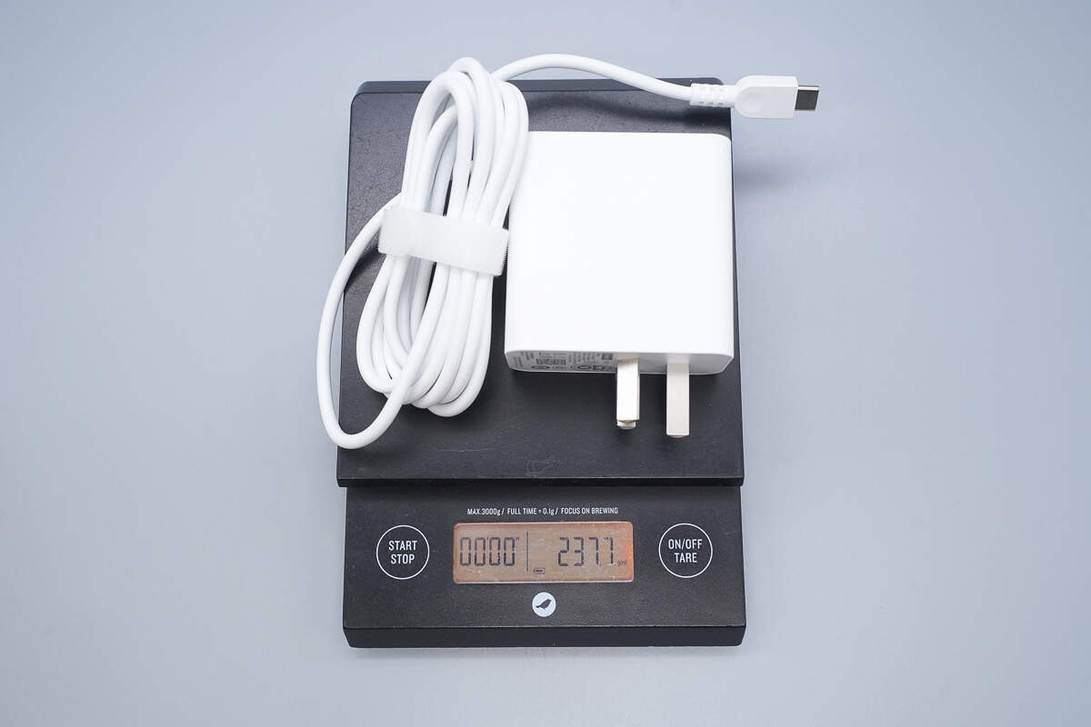
The weight is about 238 g (8.4 oz).
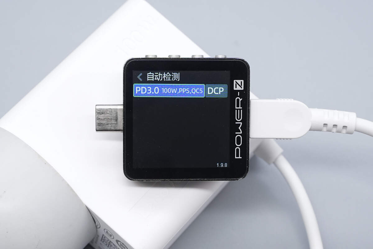
ChargerLAB POWER-Z KM003C shows it supports PD3.0, PPS, QC5, and DCP protocols.
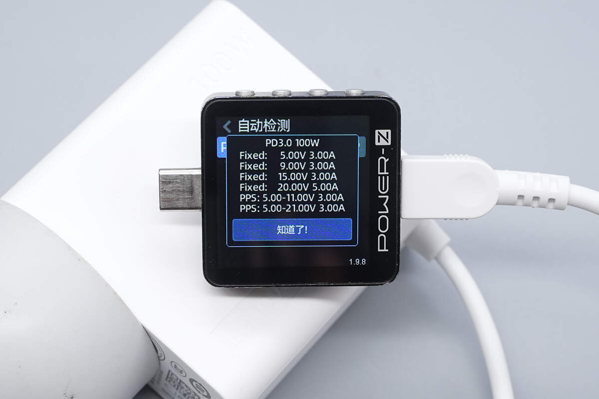
It has four fixed PDOs of 5V3A, 9V3A, 15V3A, and 20V5A. It also has two sets of PPS, which are 5-11V3A and 5-21V3A.
Teardown
Next, let's take it apart to see its internal components and structure.
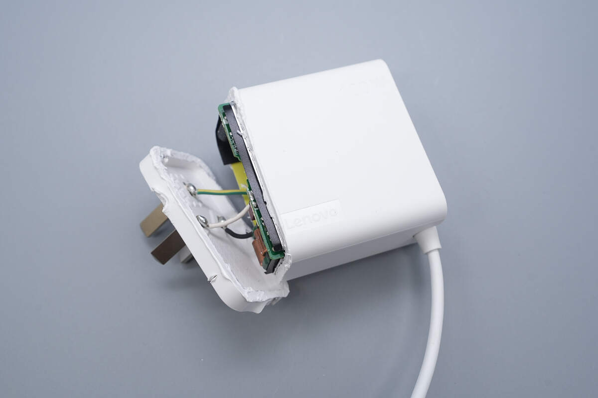
Cut open the input side of the casing. The wires are soldered to the prongs.
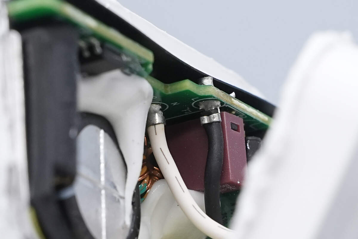
The other end of the wire is soldered to a cold-pressed terminal.
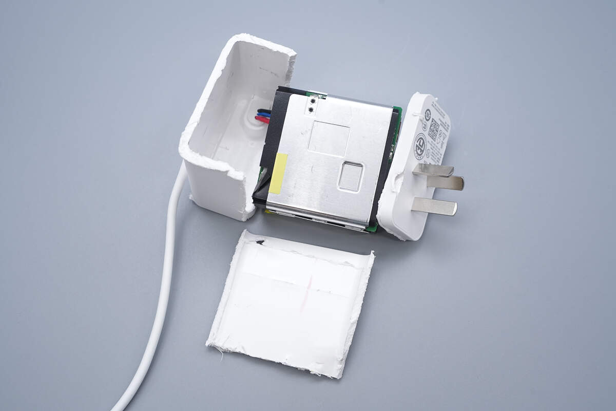
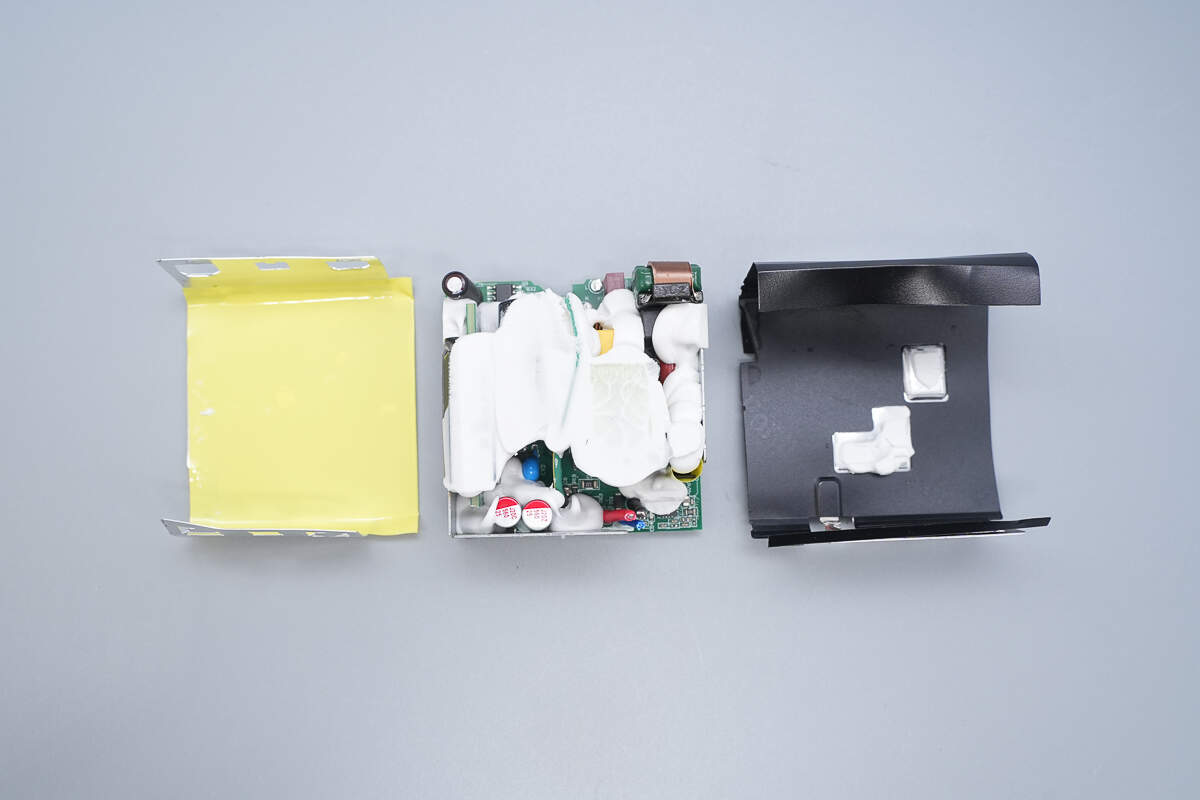
Remove the PCBA module.

The length of the PCBA module is about 56.27 mm (2.22 inches).

The width is about 56.92 mm (2.24 inches).

The thickness is about 26.62 mm (1.048 inches).
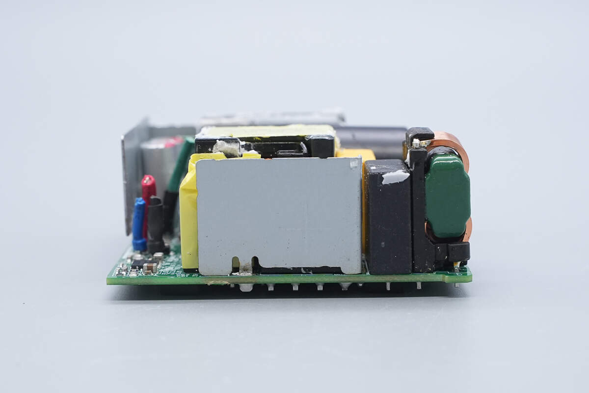
The PCBA module is enclosed by two aluminum heat sinks, secured in place with the snap-fit structure.
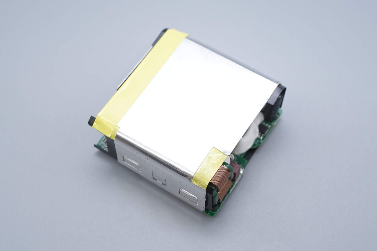
Remove the heat sinks. The inner sides are covered with insulating tape and a Mylar sheet.
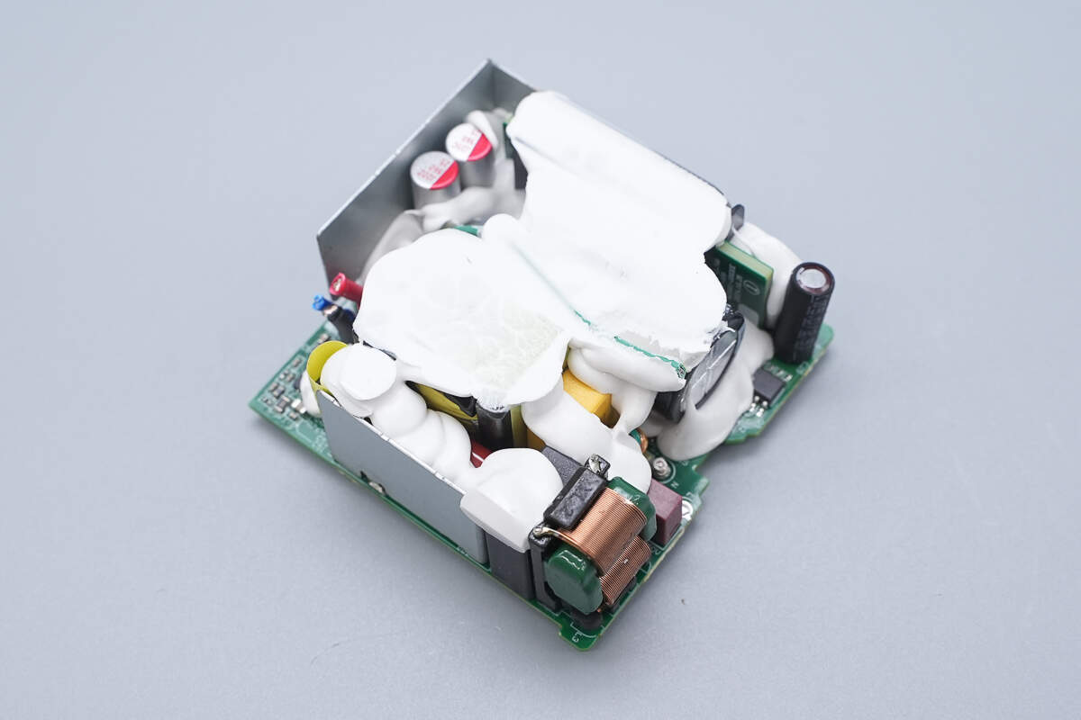
The PFC boost inductor, filter capacitors, transformer, and other components are reinforced with white adhesive.

On the backside, the PFC rectifier, primary MOSFET, and other components are also coated with adhesive.
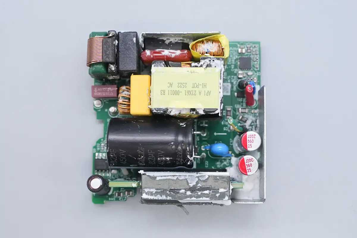
Clean off the white adhesive. The front side features film capacitors, a filter inductor, a PFC boost inductor, a high-voltage electrolytic capacitor, and a blue Y capacitor.
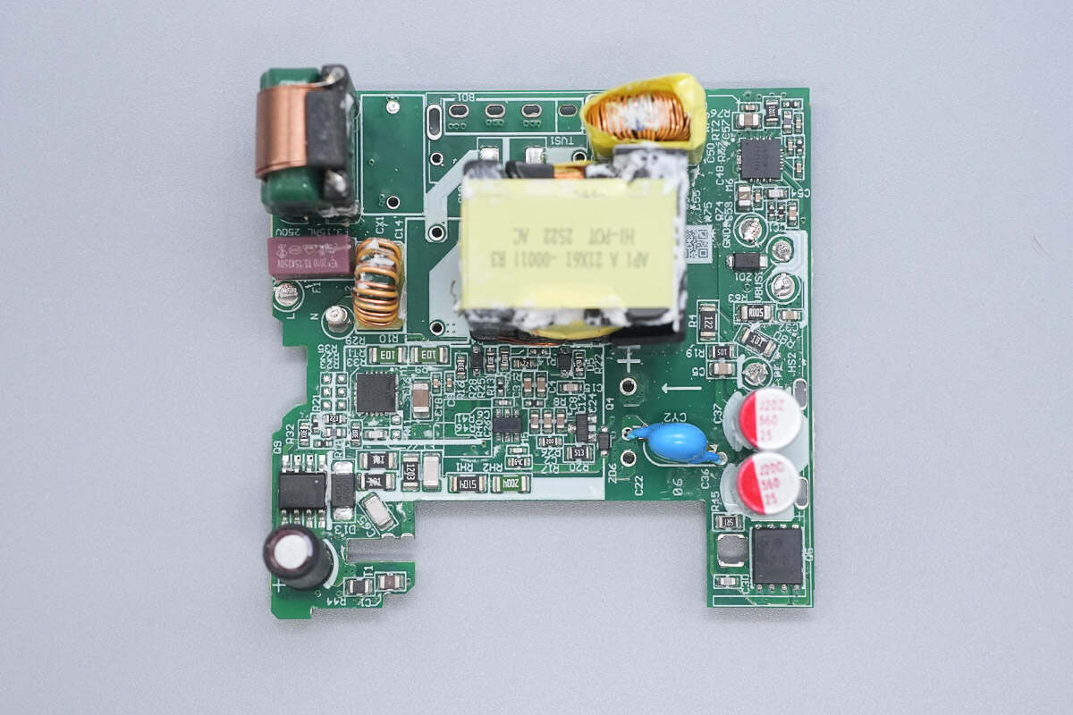
After removing some components, we can see that the front also houses the PFC boost controller, master control chip, power MOSFET, synchronous rectifier, protocol chip, and other components.

The backside contains the PFC MOSFET, primary MOSFET, optocouplers, synchronous rectification controller, VBUS MOSFET, and other components.
The heat sink on the side of the module is used for cooling the bridge rectifier.
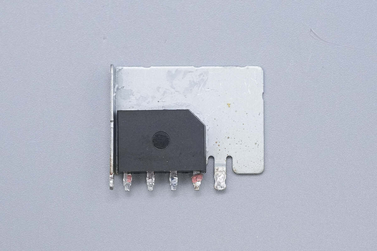
Remove the heat sink, the other side has the bridge rectifier attached.
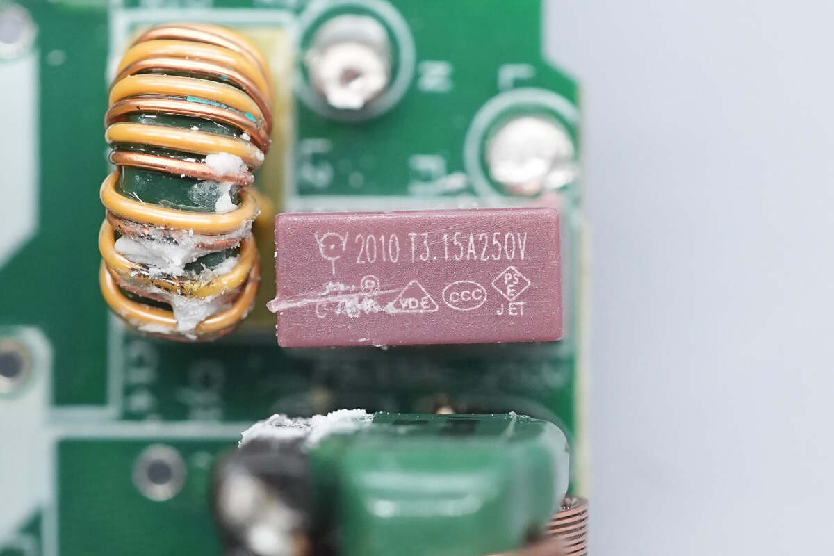
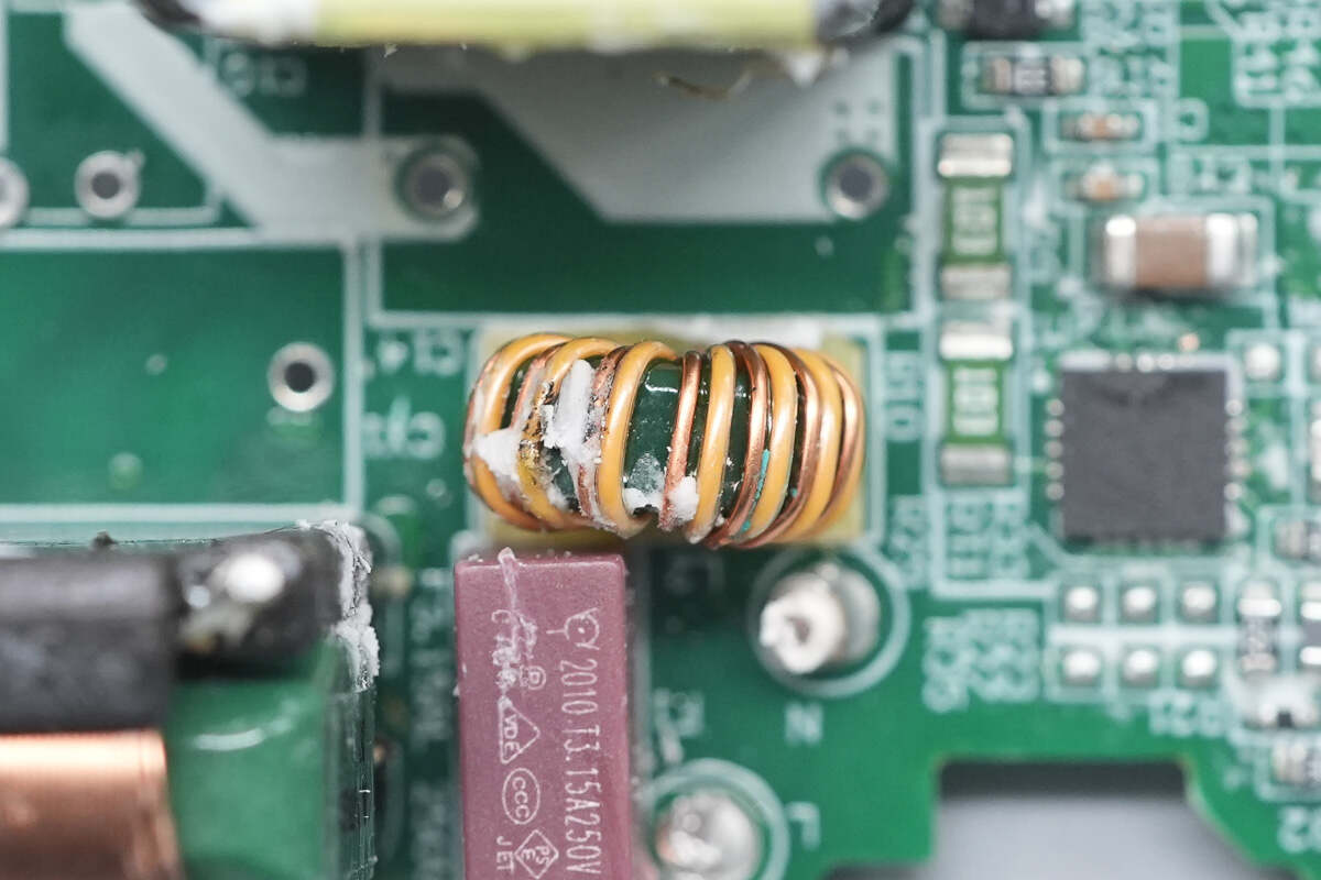
The input side features a time-delay fuse from WalterFuse, with a specification of 3.15A 250V.
The common mode choke is wound with enamel-coated wire and insulated wire, with a Bakelite board at the bottom.
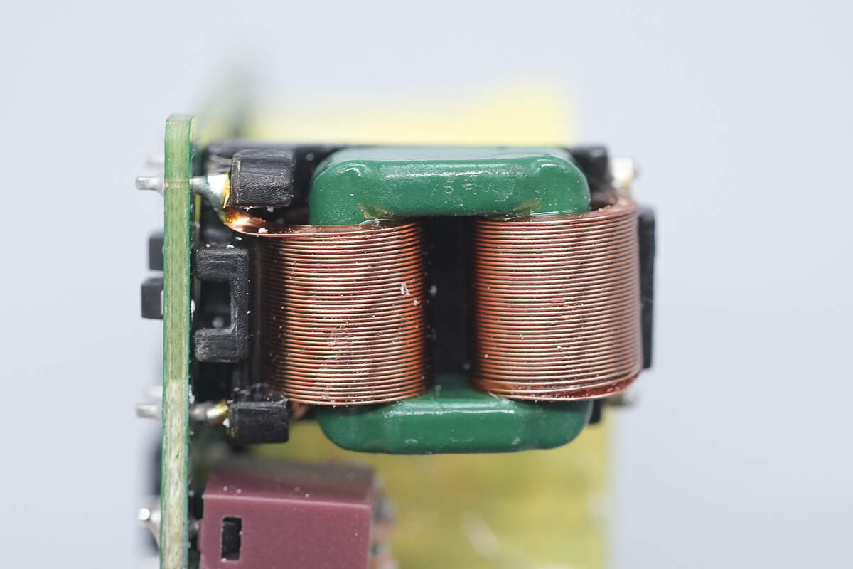
The secondary common mode choke is wound with a flat copper strip.
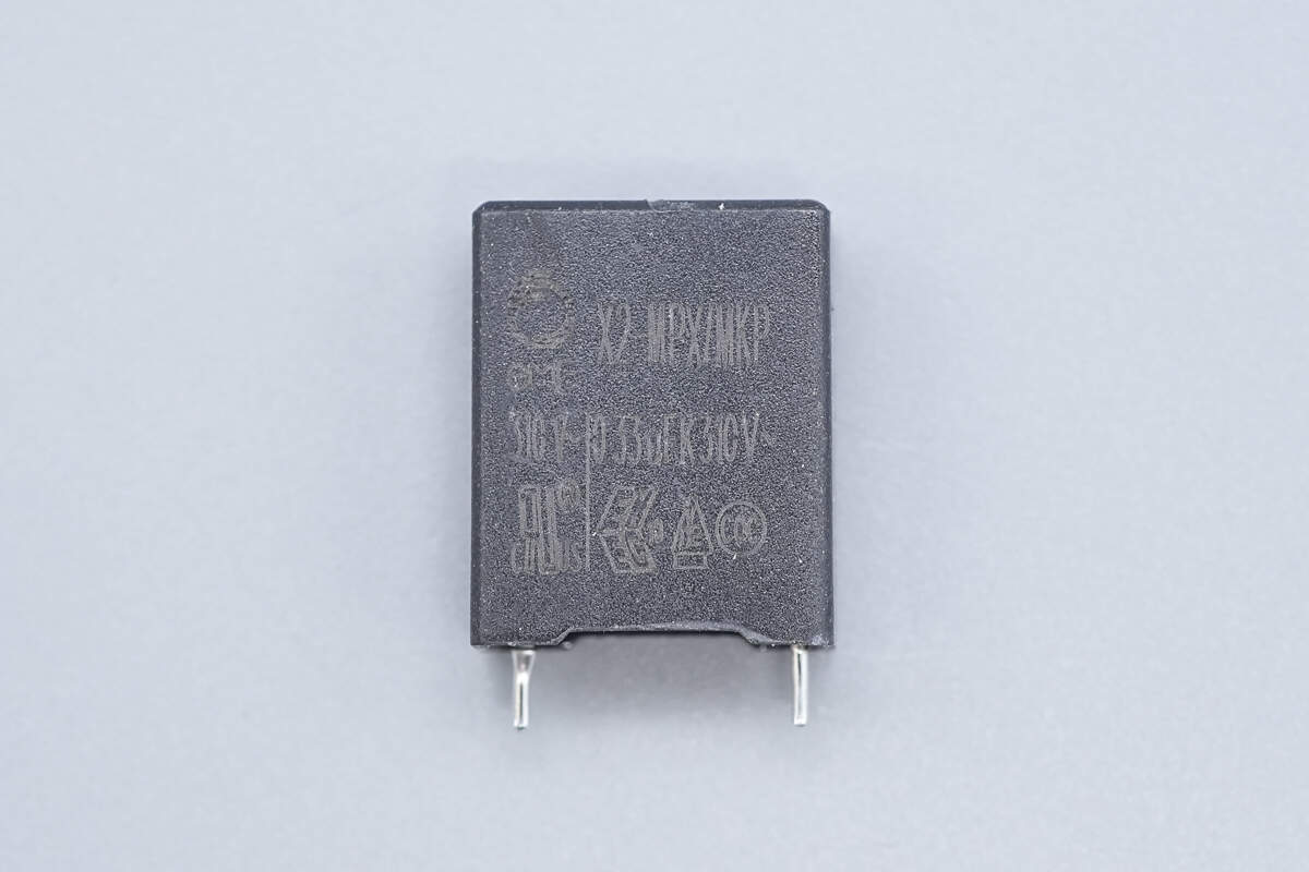
The safety X2 capacitor is from EMF, with a capacitance of 0.33μF.
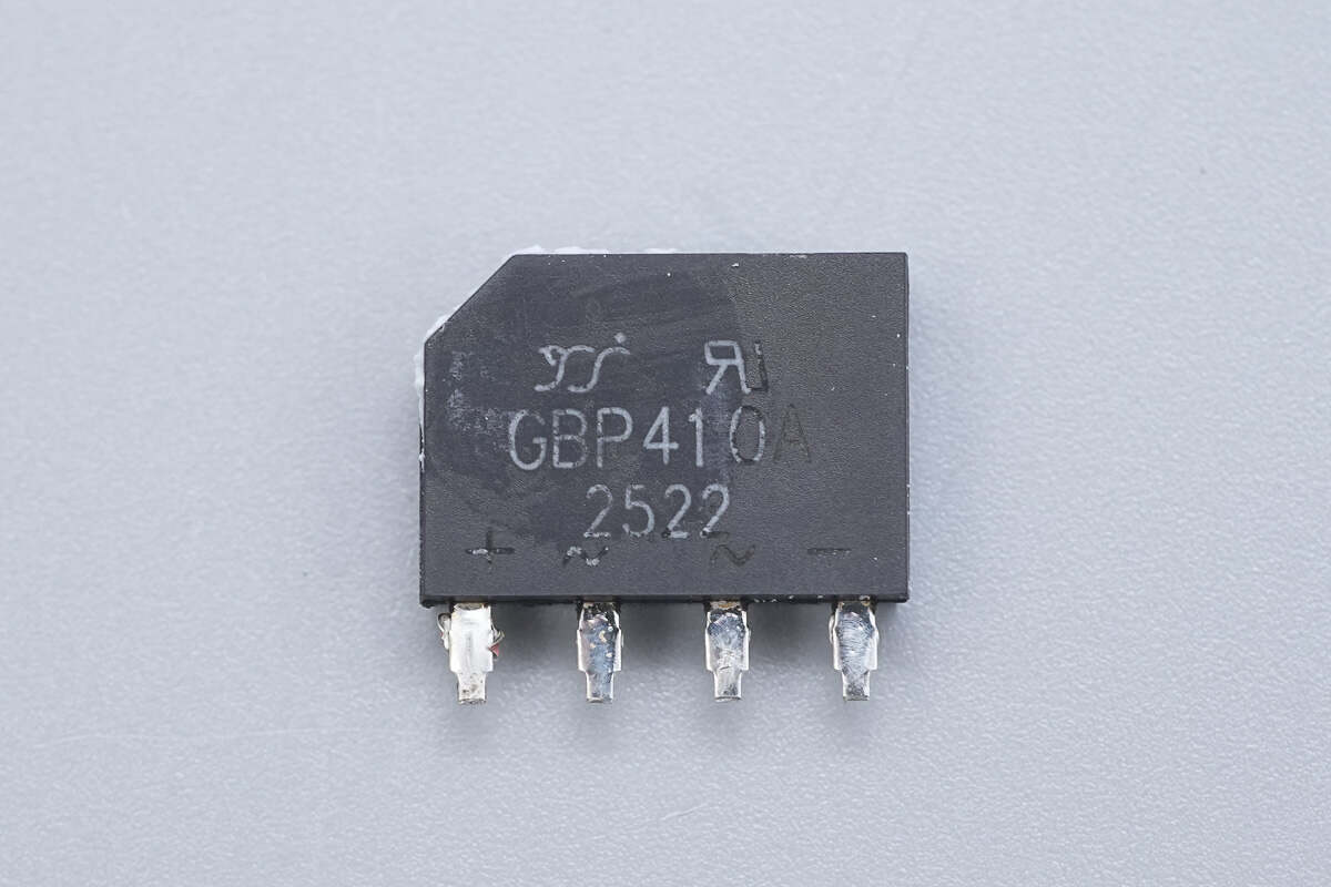
The bridge rectifier is from YJ, model GBP410A, with a specification of 4A 1000V, and it uses a GBP package.
The filter inductor is wrapped with insulating tape.
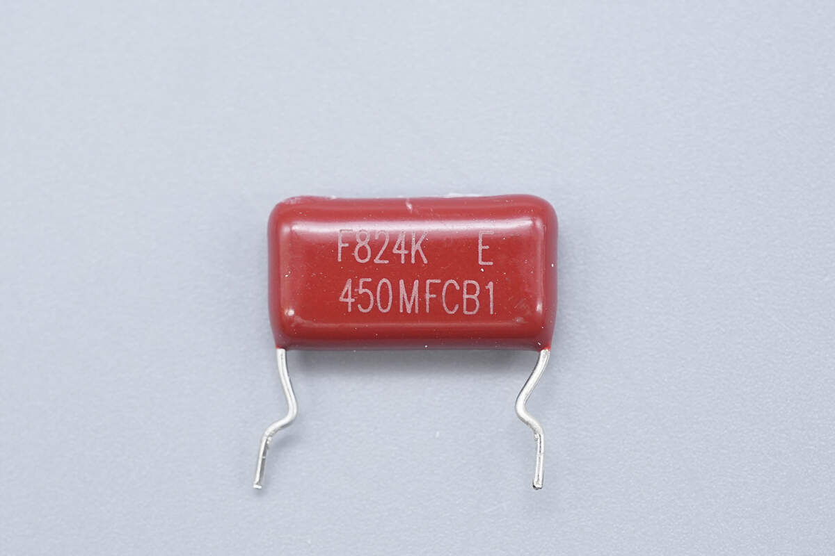
The film capacitor has a specification of 0.82μF 450V.
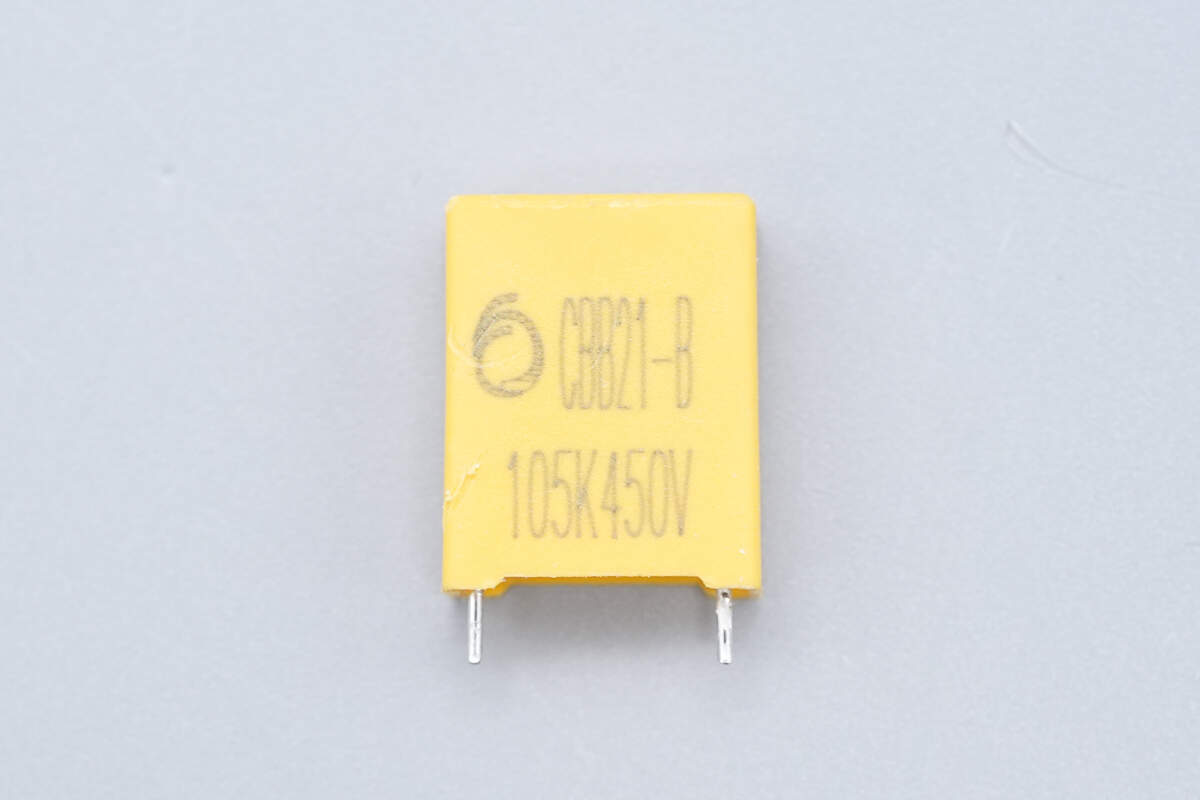
The other CBB21-B film capacitor is from EMF, with a specification of 1μF 450V.
The PFC controller is from Onsemi, marked with UPD, and the model is NCP1623. It is based on the innovative Valley Synchronous Frequency Foldback (VSFF) method. VSFF maximizes efficiency under nominal and light load conditions, operates in critical mode under heavy load, and uses discontinuous conduction mode in light load, supporting valley switching to improve efficiency.
The NCP1623 supports both critical mode and discontinuous conduction mode operation. Valley Synchronous Frequency Foldback enhances efficiency under nominal and light load, and achieves a good power factor at low switching frequencies.
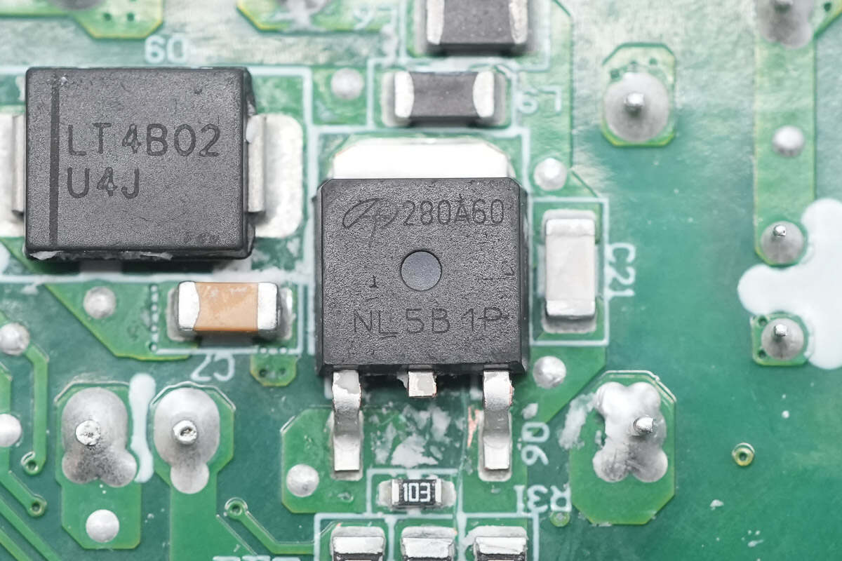
The PFC MOSFET is from AOS, model AOD280A60, with a voltage rating of 700V, a low Rds(on) of less than 0.28Ω, and comes in a TO-252 package.
Here is the information about AOS AOD280A60.

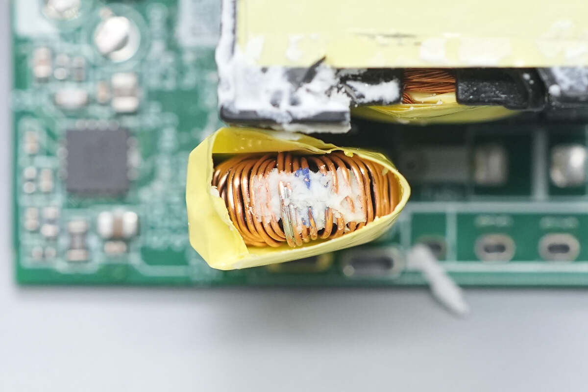
The PFC boost inductor has a plastic casing on the left side, which provides isolation from the secondary.
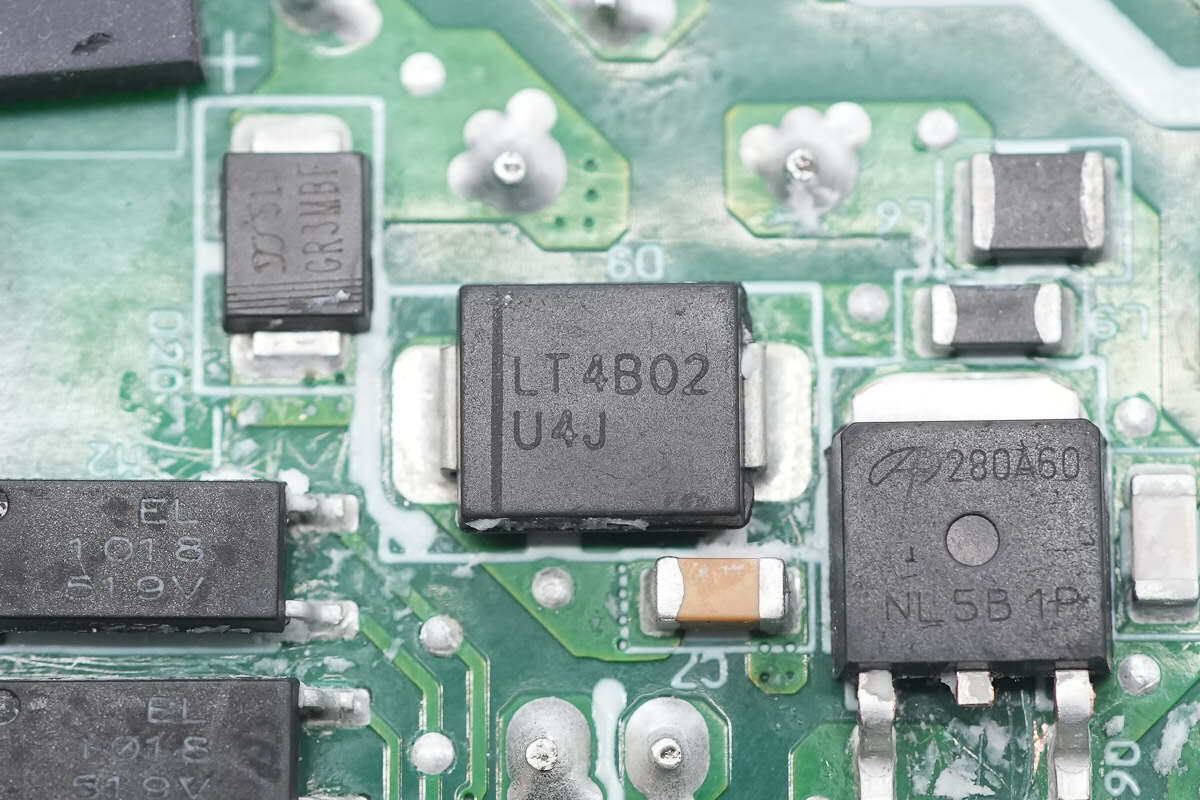
The ultrafast recovery diode marked with U4J is used for PFC boost rectification.
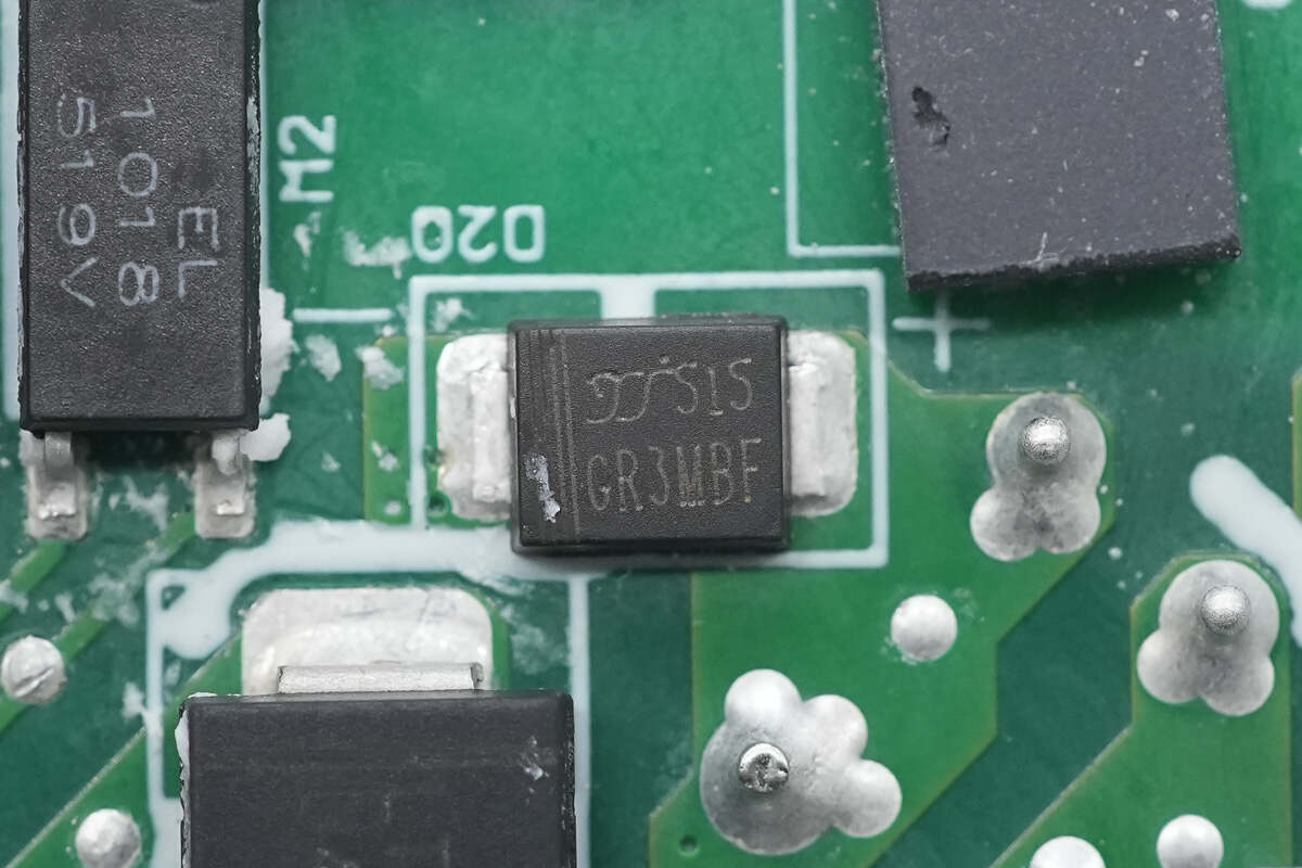
The GR3MBF diode, used for PFC bypass, is from YJ.
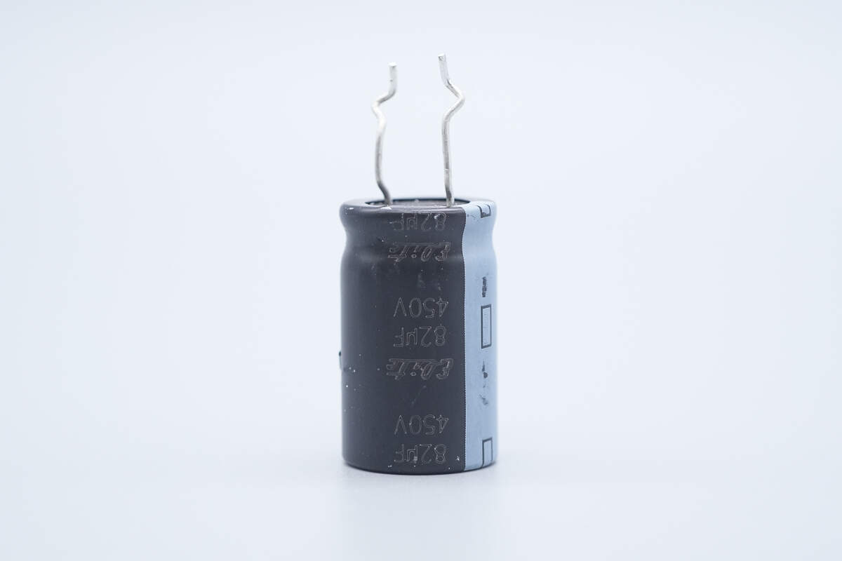
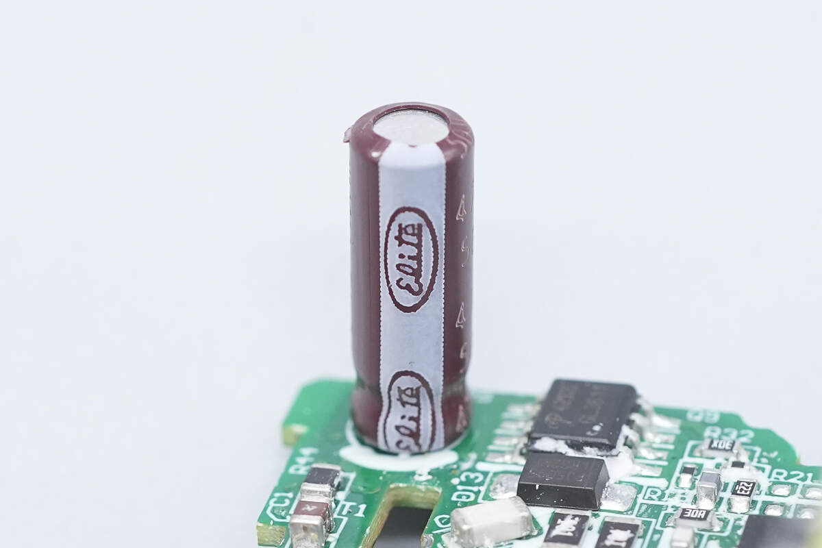
The high-voltage filter electrolytic capacitor is from ELITE, with a specification of 450V 82μF.
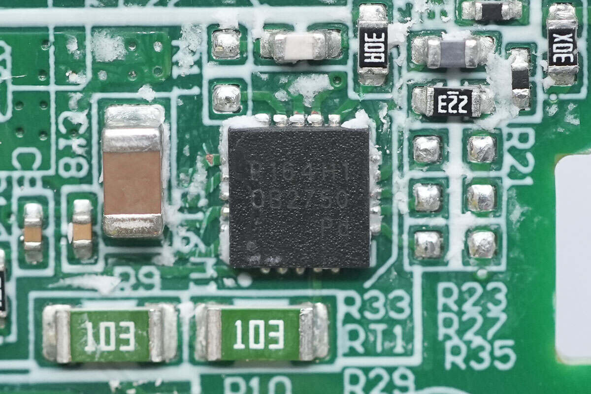
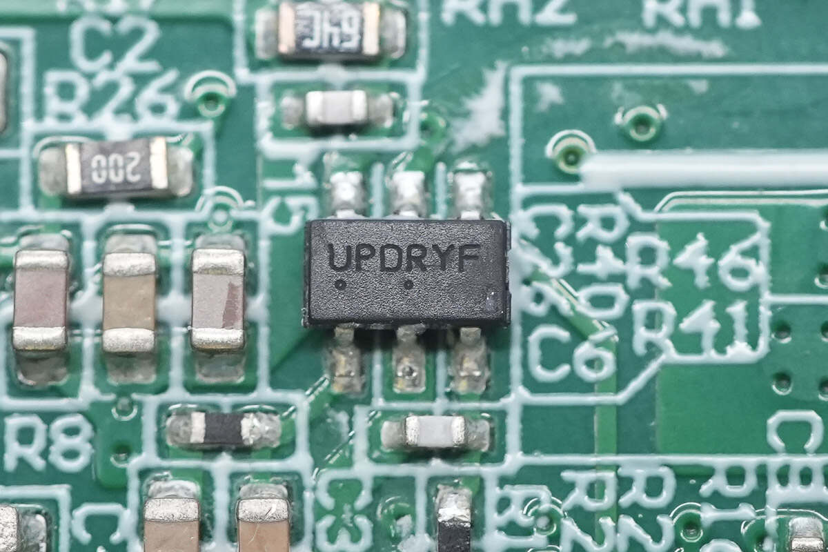
The master control chip is from On-Bright, model OB2750, and comes in a QFN20 package.
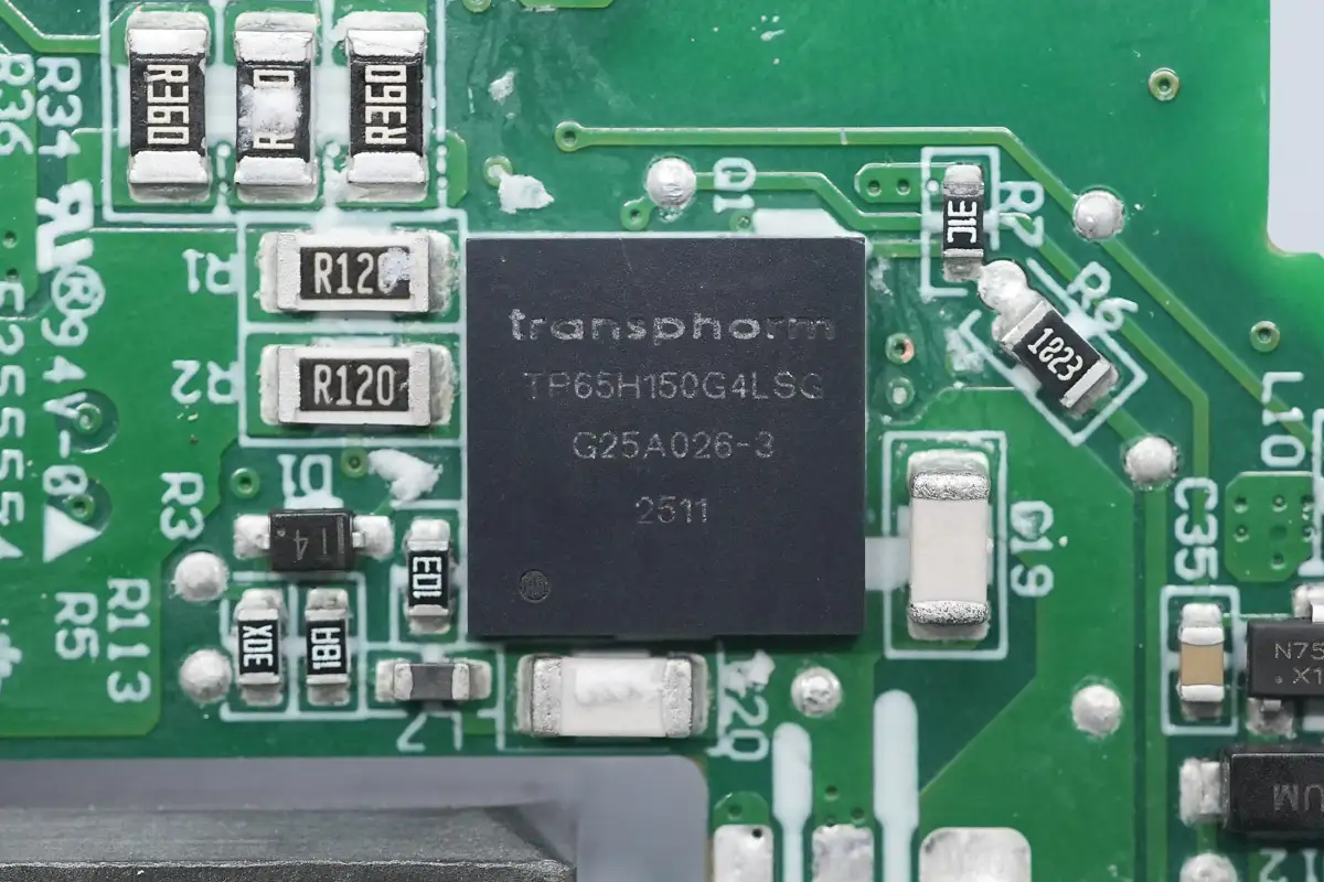
The GaN FET is from RENESAS, model TP65H150G4LSG, with a DFN8x8 package. It has a voltage rating of 650V, a transient voltage rating of 800V, and an Rds(on) of 150mΩ. The gate can withstand 18V, offering very low reverse recovery charge and reduced switching losses. Compared to traditional silicon devices, it improves efficiency and switching frequency, enhances system power density, reduces system size and weight, and lowers system cost. It is suitable for applications such as fast-charging power supplies and LED lighting.
The filter capacitor supplying power to the master control chip is from ELITE.
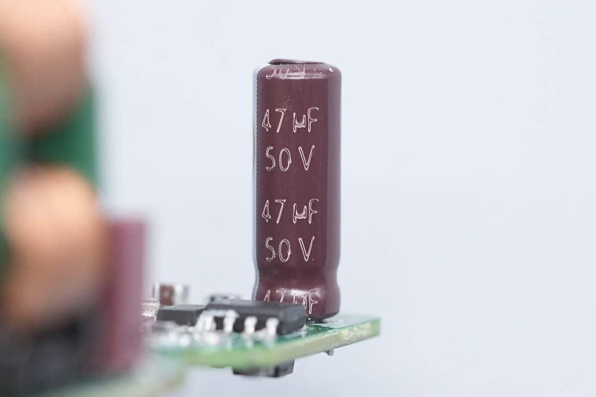
The specification is 50V 47μF.
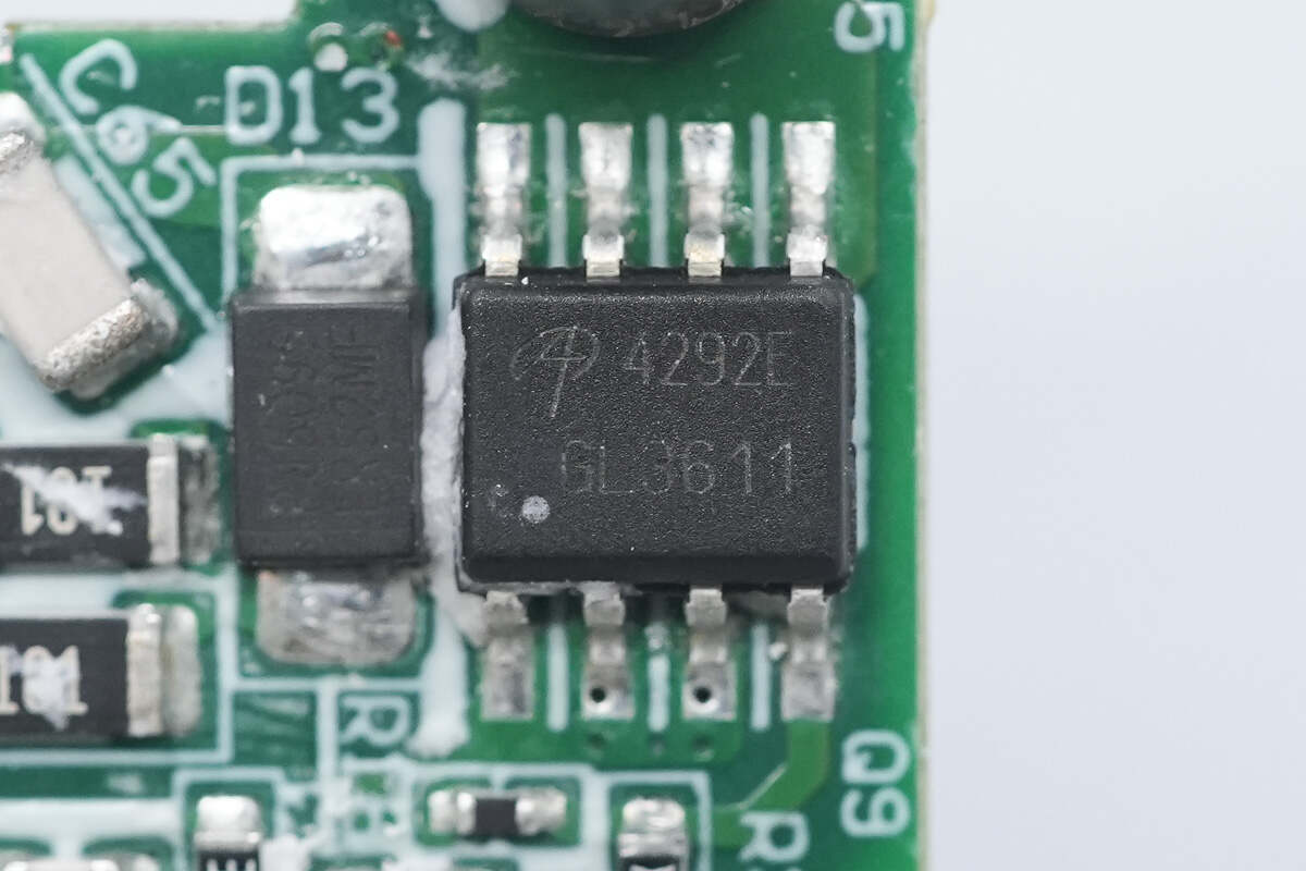
The power MOSFET is from AOS, model AO4292E, an NMOS with a voltage rating of 100V, a Rds(on) of 23mΩ, and comes in an SO-8 package.
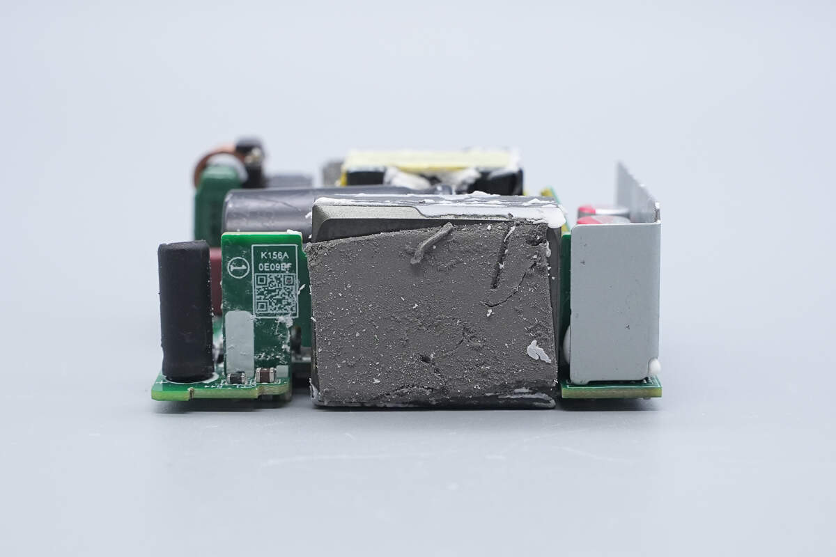
The planar transformer module has a thermal pad attached to the core for heat dissipation.
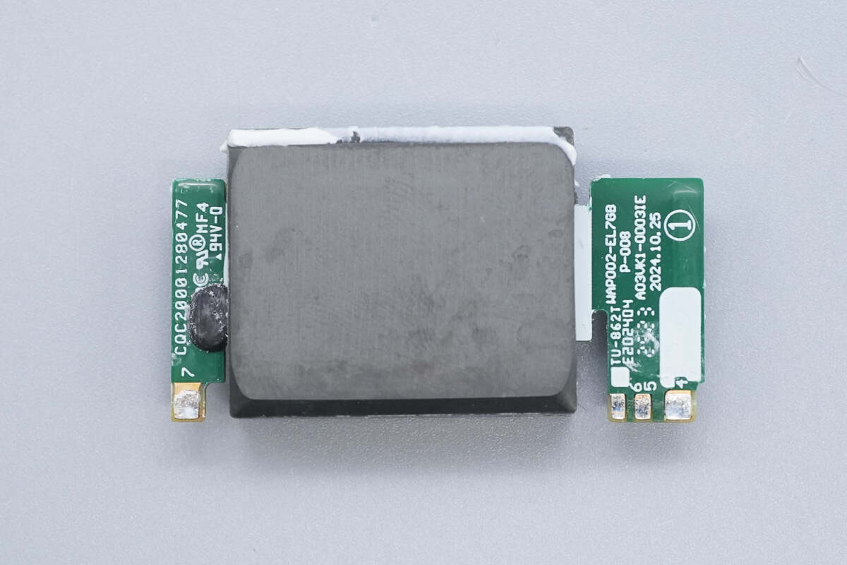
Close-up of the planar transformer module.
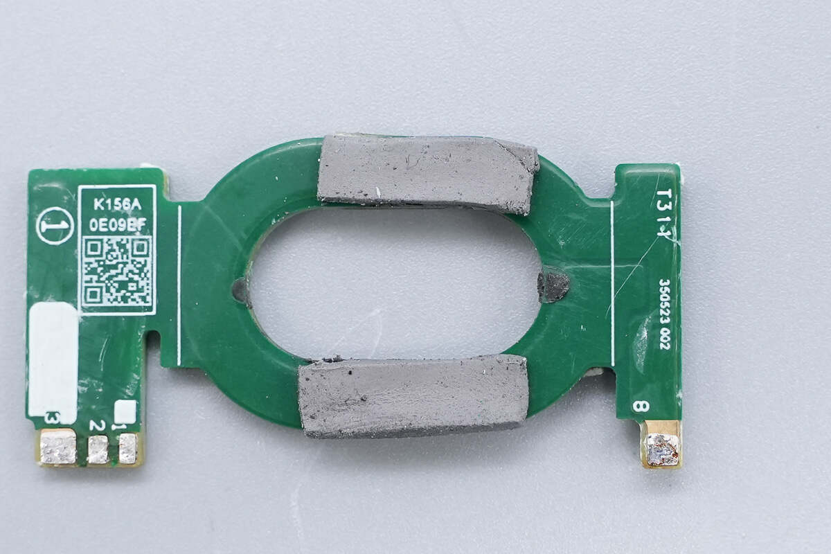
After breaking the core, the planar transformer reveals that the racetrack-shaped coil inside is equipped with thermal pads.
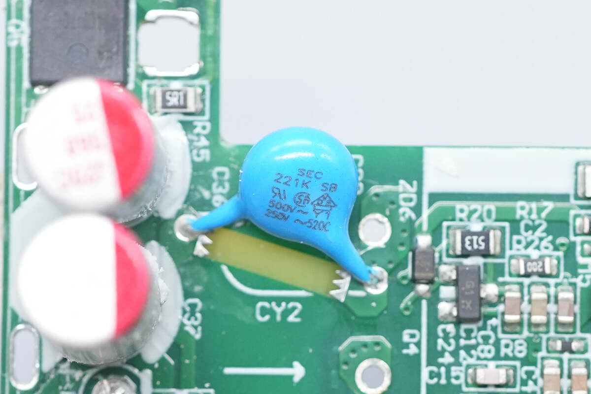
The blue Y capacitor is from SEC.
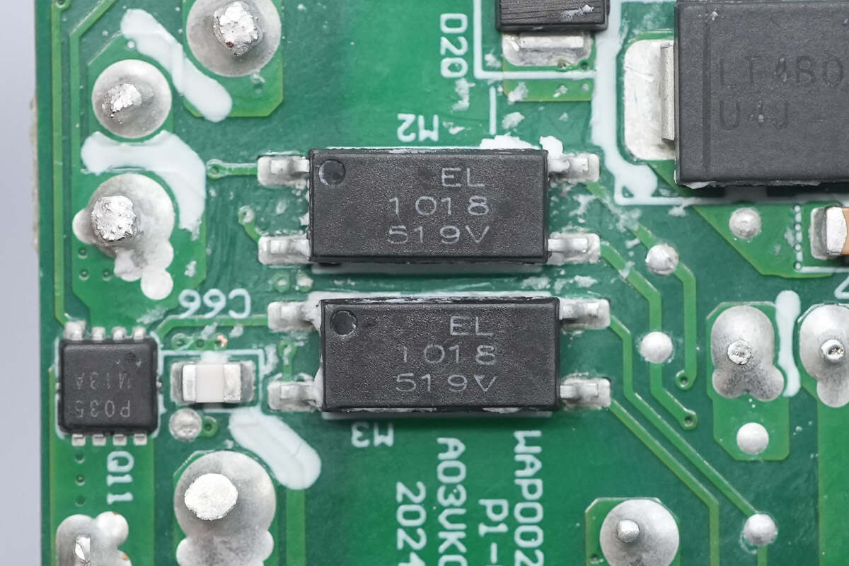
Close-up of the two Everlight EL 1018 optocouplers.
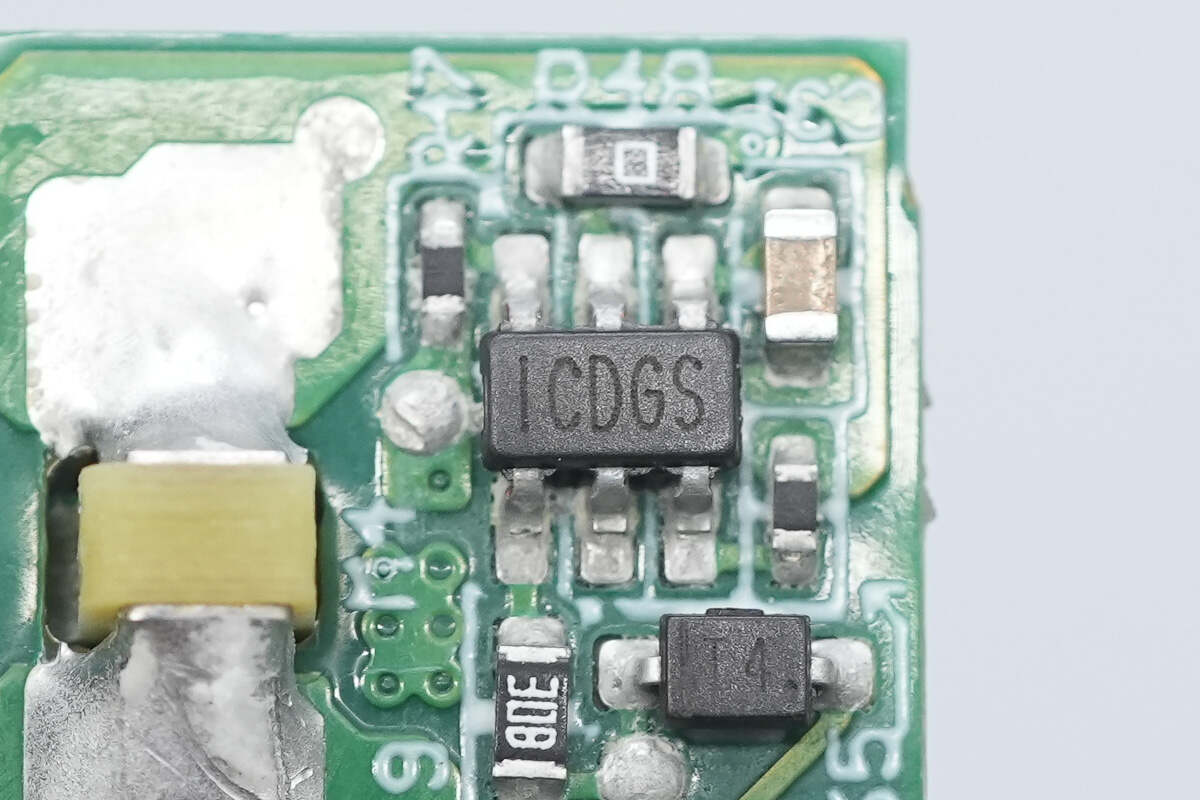
The synchronous rectifier controller is marked with ICDGS.
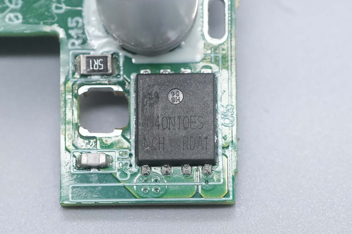
The synchronous rectifier is from Pingwei, model PW040N10ES, an NMOS with a voltage rating of 100V, a Rds(on) of 3.4mΩ, and comes in a DFN5x6 package.
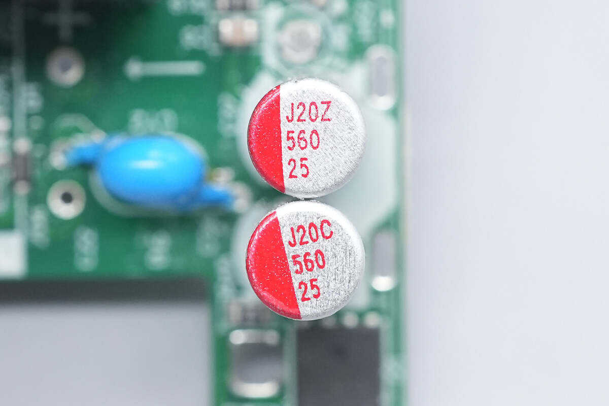
The two solid capacitors for output filtering have a specification of 25V 560μF.
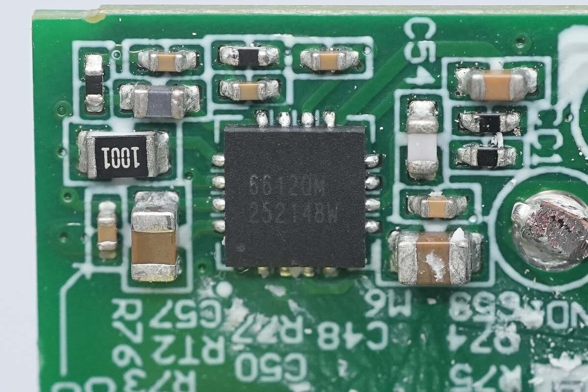
The protocol chip uses Leadtrend LD6612QM, offering high integration to reduce external components, making it a cost-effective and size-efficient solution. It combines USB-PD baseband PHY, Type-C cable detection, parallel voltage regulators, voltage and current monitoring, load switch NMOS control circuitry, and a microcontroller. The built-in voltage regulator allows the chip to operate within a voltage range of 3V to 24V. The supported protocols include PD3.0, PPS, FCP/SCP, QC5/QC4+/QC3.0/QC2.0, Apple 5V2.4A, BC1.2, and more.
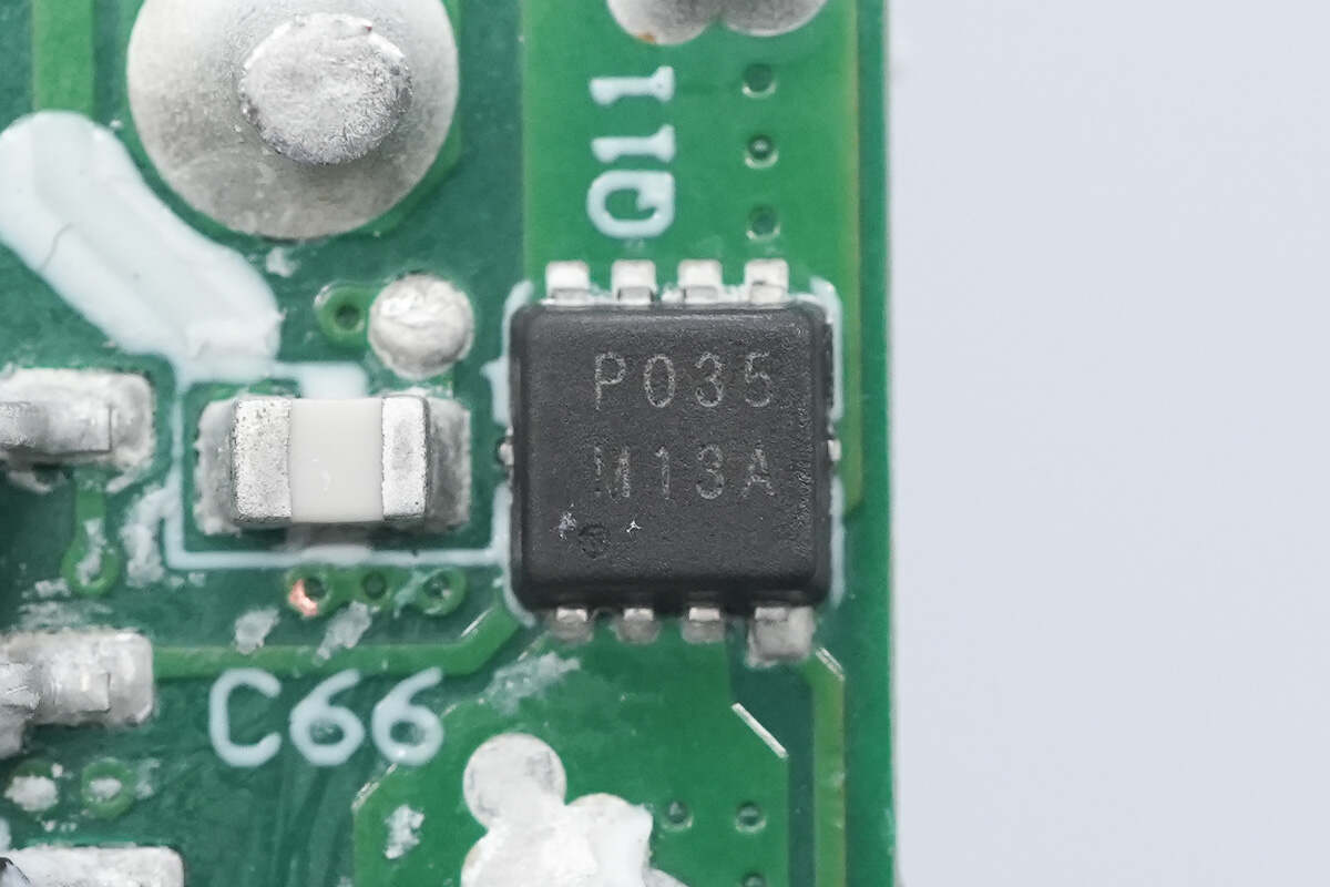
The output VBUS MOSFET is from Silan, marked with P035, model SVTP035R5NL3. It is an NMOS with a voltage rating of 30V, a Rds(on) of 4mΩ, and comes in a PDFN 3x3 package.
Well, those are all components of the Lenovo 100W GaN Power Adapter.
Summary of ChargerLAB
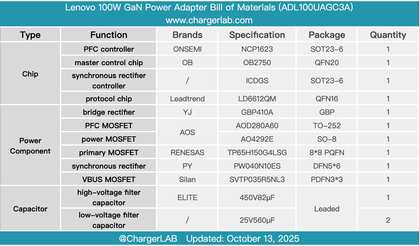
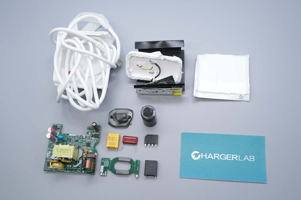
Here is the component list of the Lenovo 100W GaN Power Adapter for your convenience.
It features a three-prong plug and comes with a 1.8-meter output cable. It supports 100W PD fast charging and also supports 21V3A PPS fast charging.
After taking it apart, we found that it adopts a PFC+QR flyback architecture design. The PFC controller uses the Onsemi NCP1623, paired with the AOS AOD280A60 PFC MOSFET. The master control is handled by the On-Bright OB2750, with the RENESAS TP65H150G4LSG GaN device.
The module is wrapped with aluminum sheets to enhance heat dissipation. Additional heat sinks are installed for the bridge rectifier, synchronous rectifier, and other power devices. The components are also secured with adhesive. These design choices address the heating issues commonly encountered in laptop charging and high-power continuous output scenarios.
Related Articles:
1. Teardown of UUGreenPower UR100020‑SW 20 kW Ultra‑Wide Voltage Constant Power Charging Module
2. Teardown of Dell 280W USB-C GaN AC Adapter (LA280PM240)
3. Teardown of Bel Fuse 3000W GaN Server Power Supply (TET3000-12-069RA)