Introduction
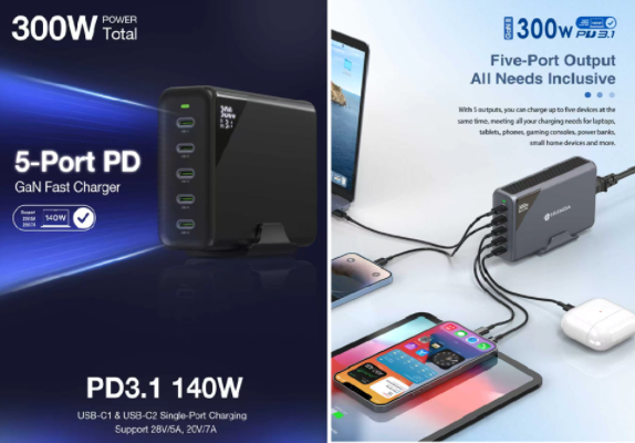
Recently, we got our hands on a 300W 5-port GaN desktop charger from HUNDA. It features a detachable input cable and is equipped with four USB-C ports and one USB-A port, offering up to 300W of total output power to support simultaneous charging of laptops, tablets, smartphones, and more.
Two of the USB-C ports support 140W PD 3.1 fast charging and are also compatible with the latest UFCS, further enhancing their practicality. It is designed based on the ZIENER ZN65C1R120L GaN solution, offering higher system reliability and efficiency. Let’s take a closer look at its internal design.
Product Appearance
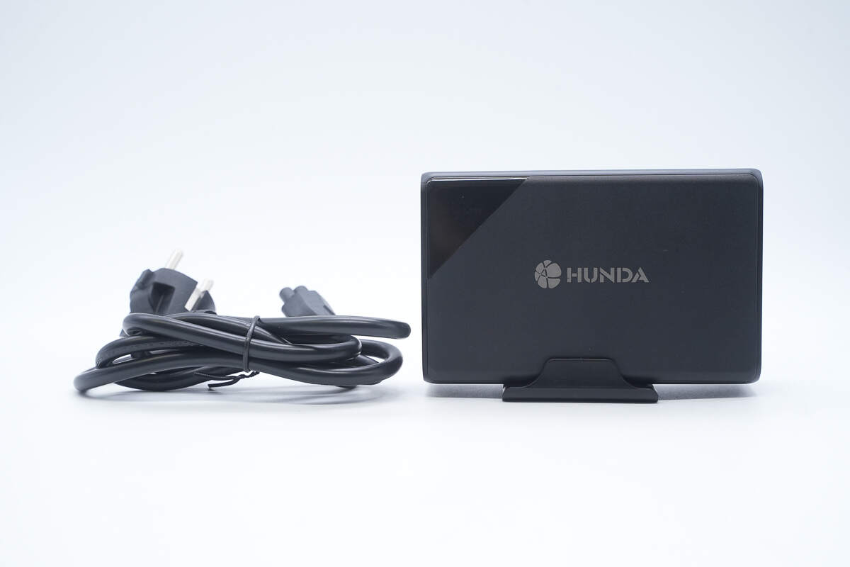
The detachable input cable design allows users to easily replace the power cord to suit a wider range of countries and regions.
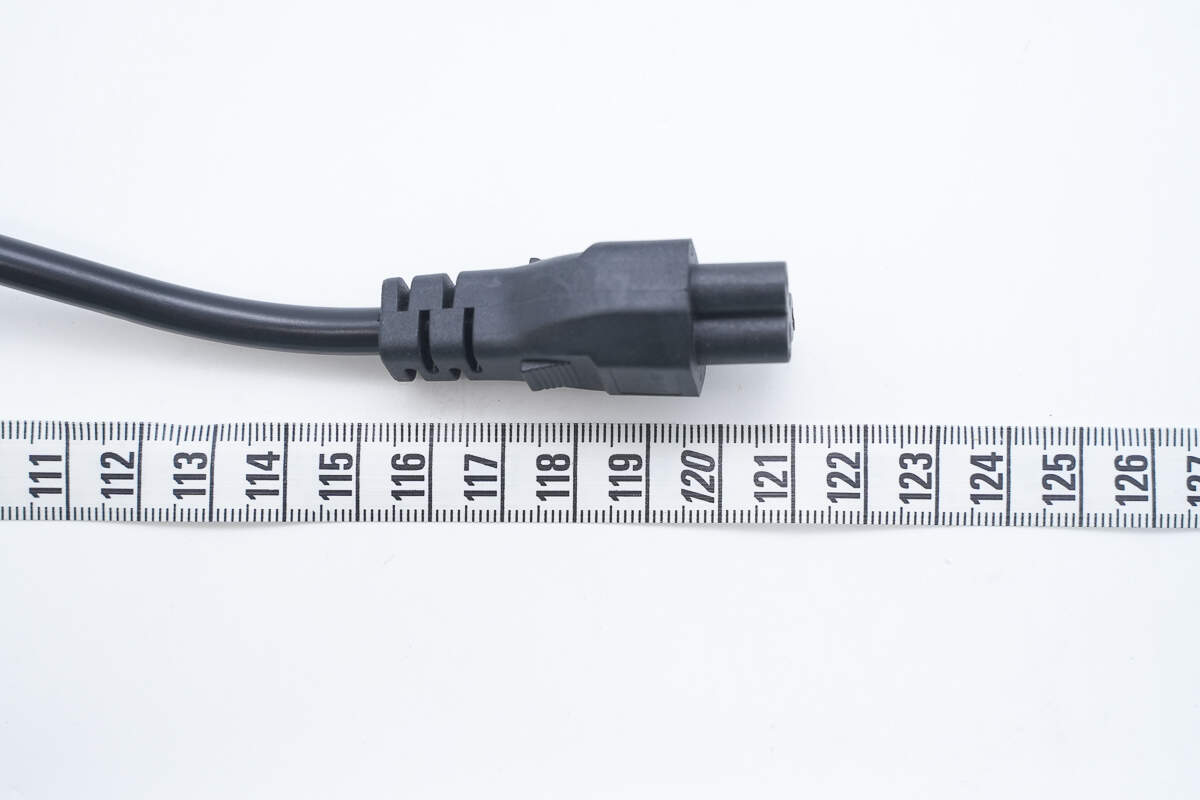
The length of the power cord is about 121 cm (47.64 inches).
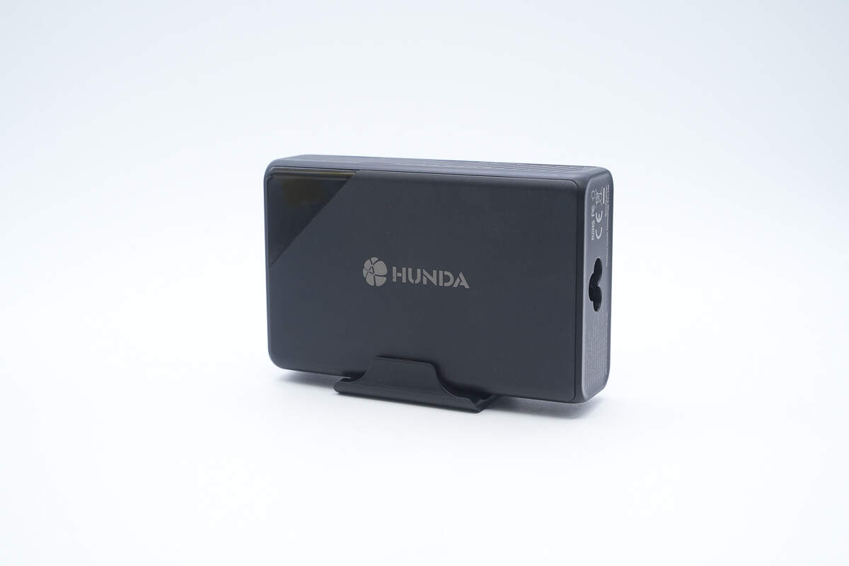
The casing is made of flame-retardant PC material with a matte, fingerprint-resistant surface. It comes with a stand that allows the charger to be positioned upright, keeping your desk neat and organized.
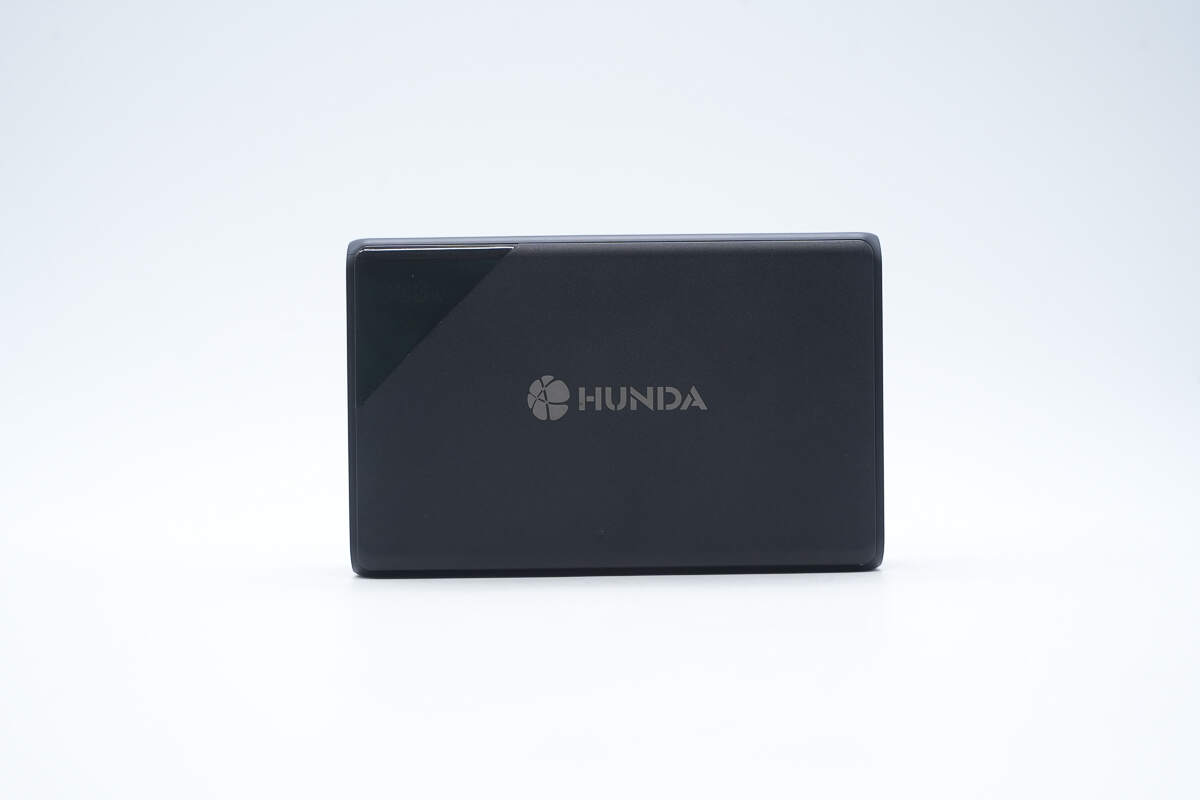
The front center of the charger is printed with the HUNDA logo.
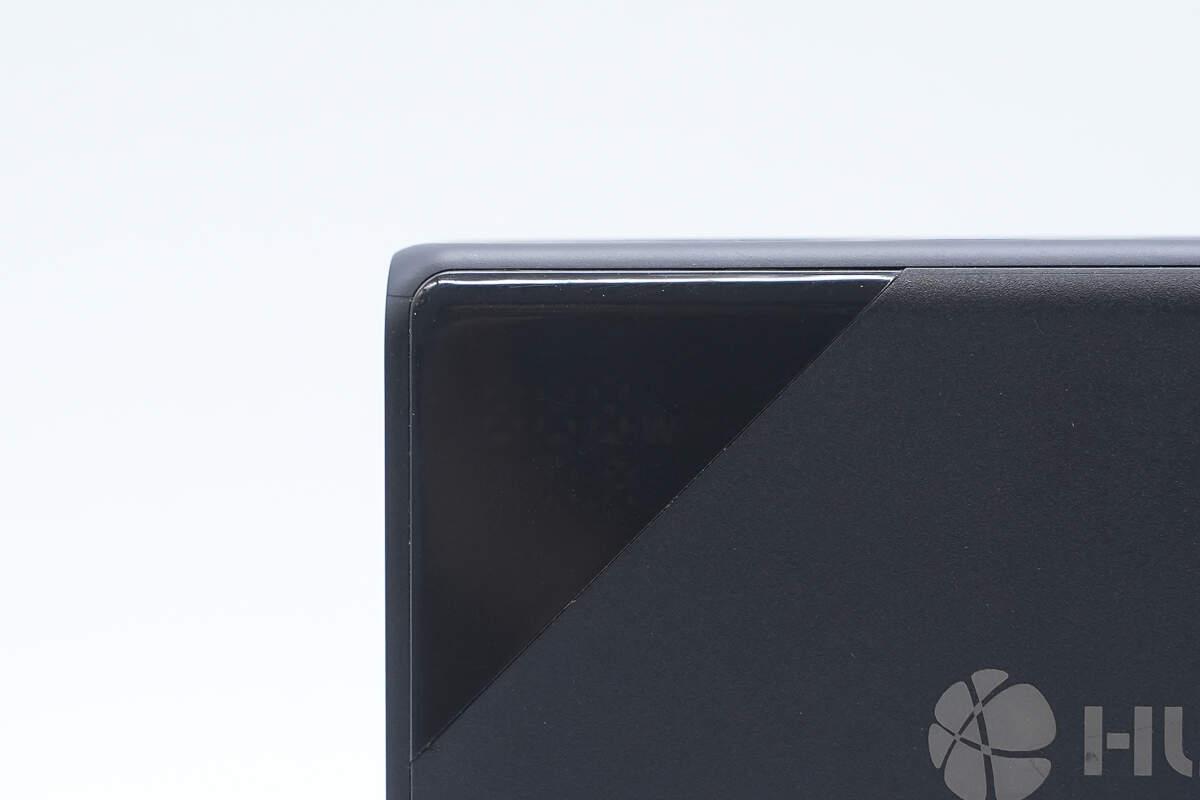
The glossy area at the top left corner houses a hidden digital display.
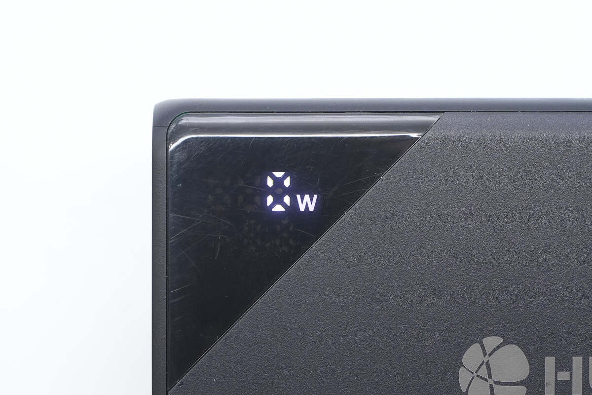
The digital display can show the real-time output power, making it easy to monitor the charging status.
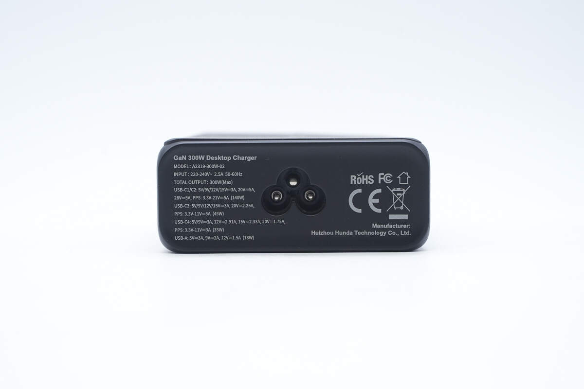
The input end is printed with the specifications.
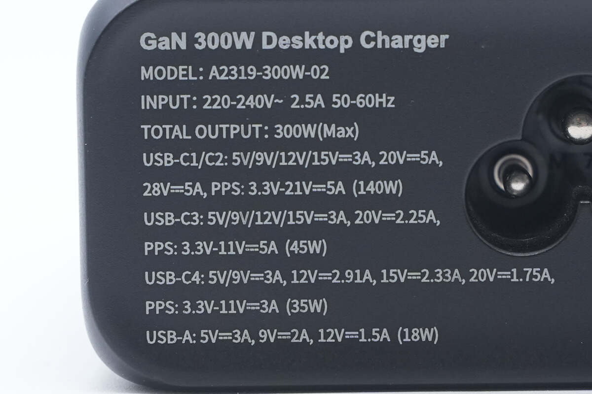
Model: A2319-300W-02
Input: 220-240V\~2.5A 50/60Hz
Total Output: 300W (Max)
USB-C1/C2: 5/9/12/15V 3A, 20V 5A, 28V 5A
PPS: 3.3-21V 5A (140W)
USB-C3: 5/9/12/15V 3A, 20V 2.25A
PPS: 3.3-11V 5A (45W)
USB-C4: 5/9V 3A, 12V 2.91A, 15V 2.33A, 20V 1.75A
PPS: 3.3-11V 3A (35W)
USB-A: 5V 3A, 9V 2A, 12V 1.5A (18W)
It has passed CE and FCC certifications.
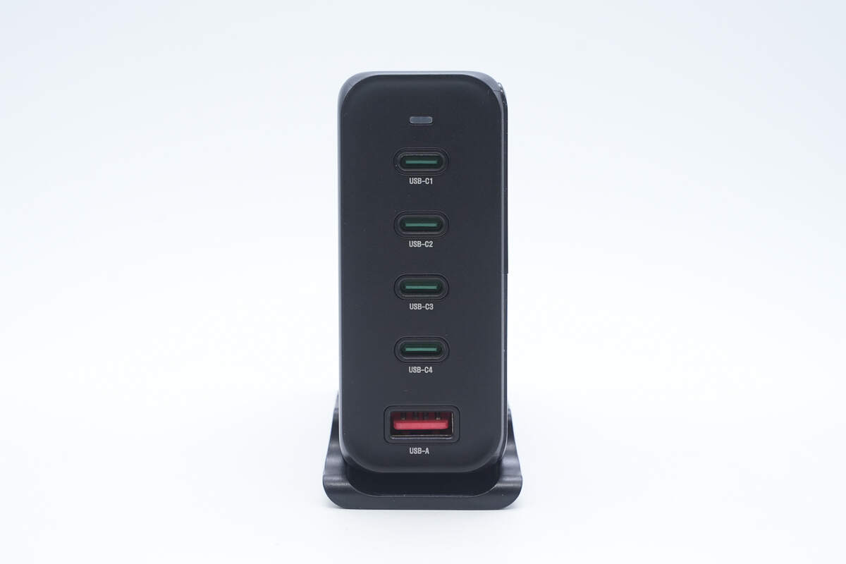
It is equipped with four USB-C ports, one USB-A port, and an LED indicator.
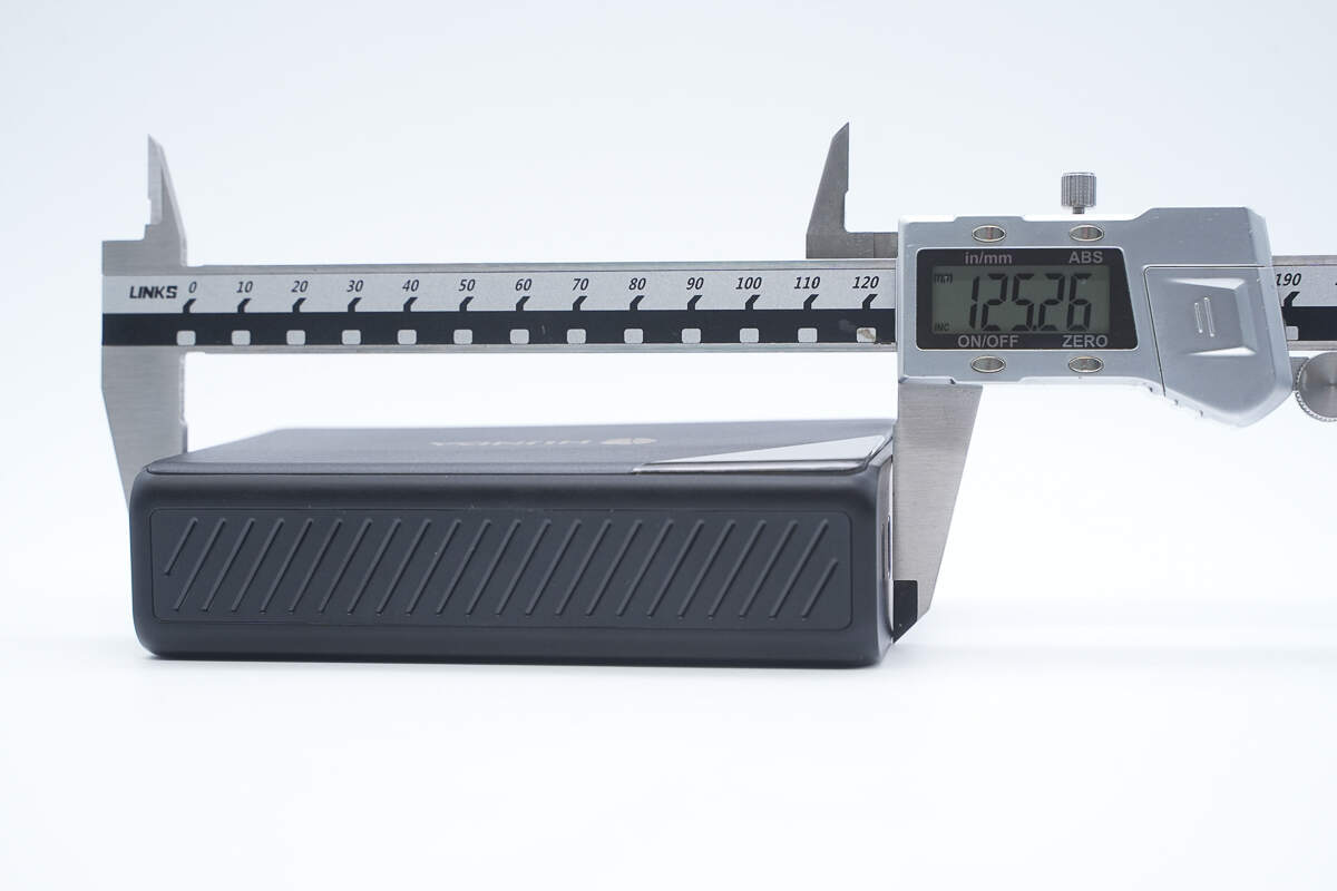
The length of the charger is about 125.26 mm (4.93 inches).
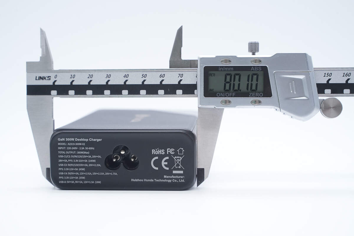
The width is about 80.1 mm (3.15 inches).
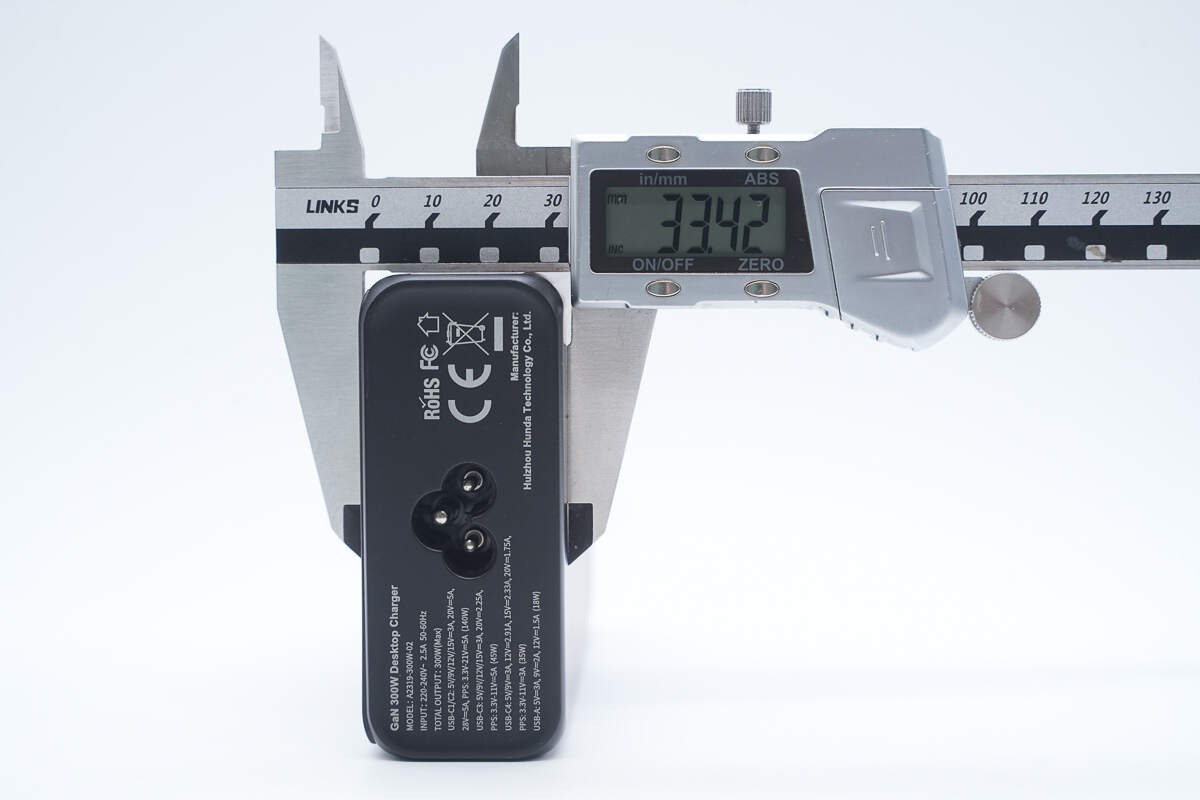
The thickness is about 33.42 mm (1.32 inches).
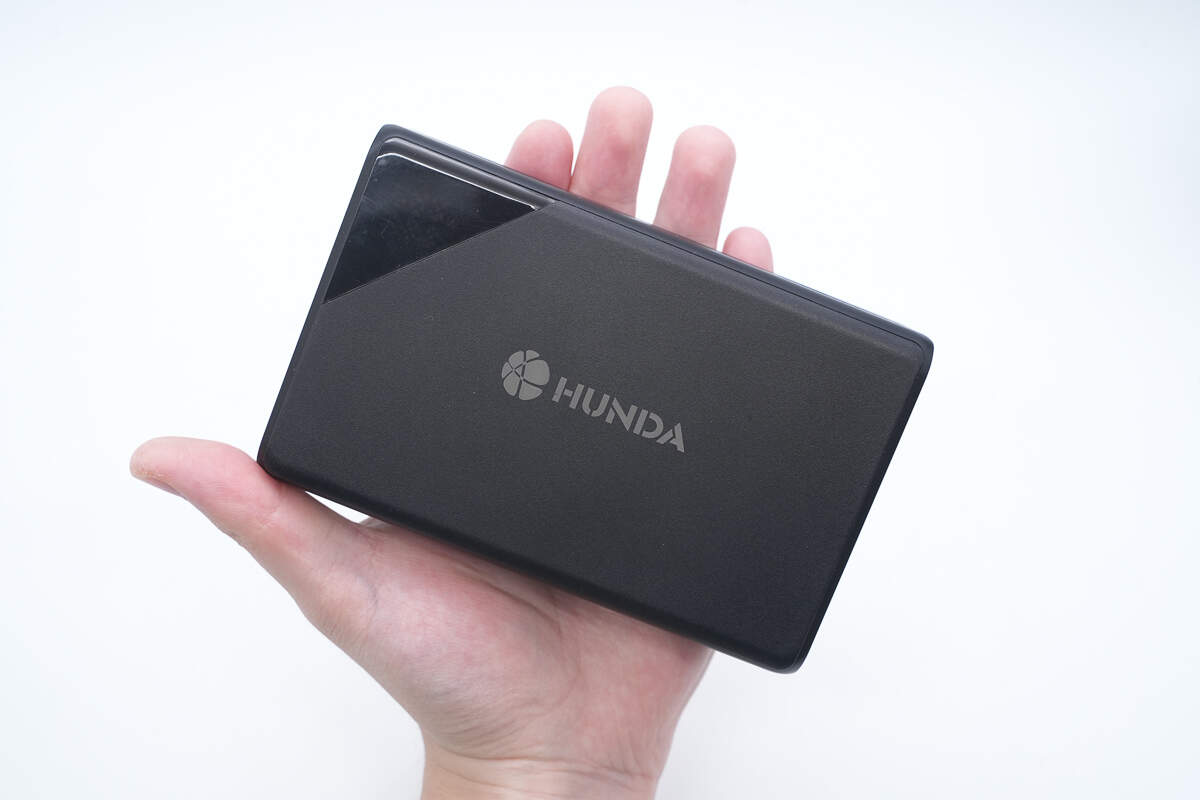
That's how big it is in the hand.
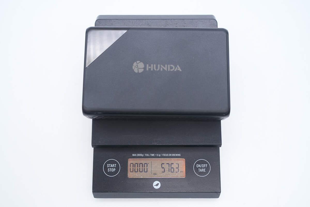
The weight is about 576 g (20.32 oz).
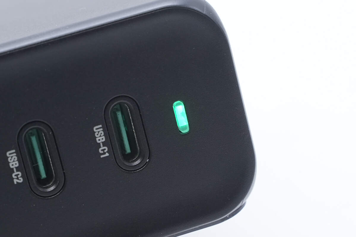
The indicator lights up green when powered on.
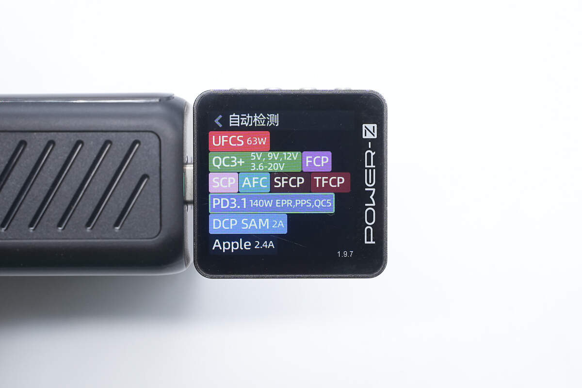
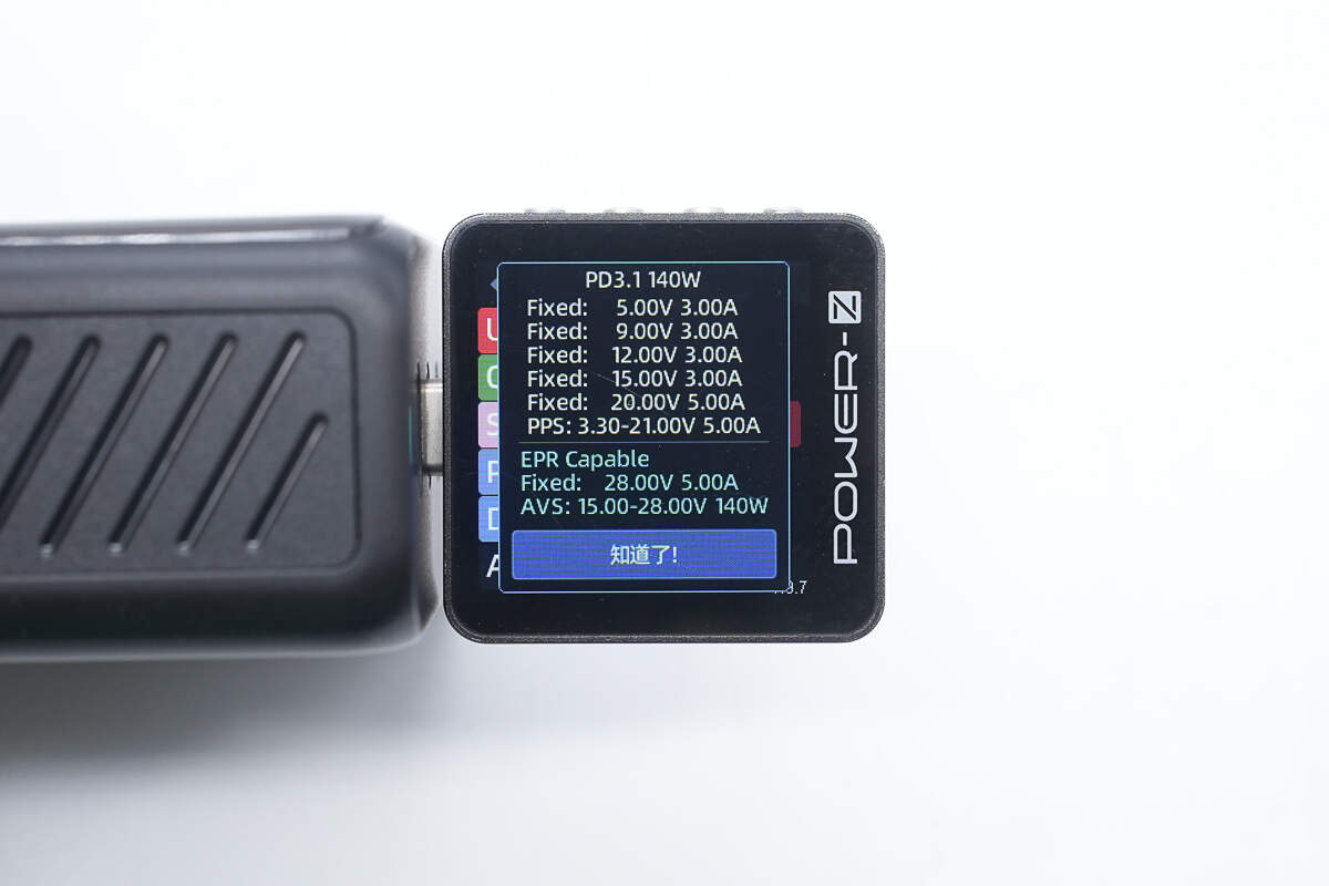
ChargerLAB POWER-Z KM003C shows that the USB-C1 supports UFCS, QC3+/5, FCP, SCP, AFC, SFCP, TFCP, PD3.1, PPS, DCP, SAM 2A, and Apple 2.4A charging protocols.

And it has six fixed PDOs of 5V3A, 9V3A, 12V3A, 15V3A, 20V5A, and 28V5A, as well as one set of AVS, which is 15-28V 140W.
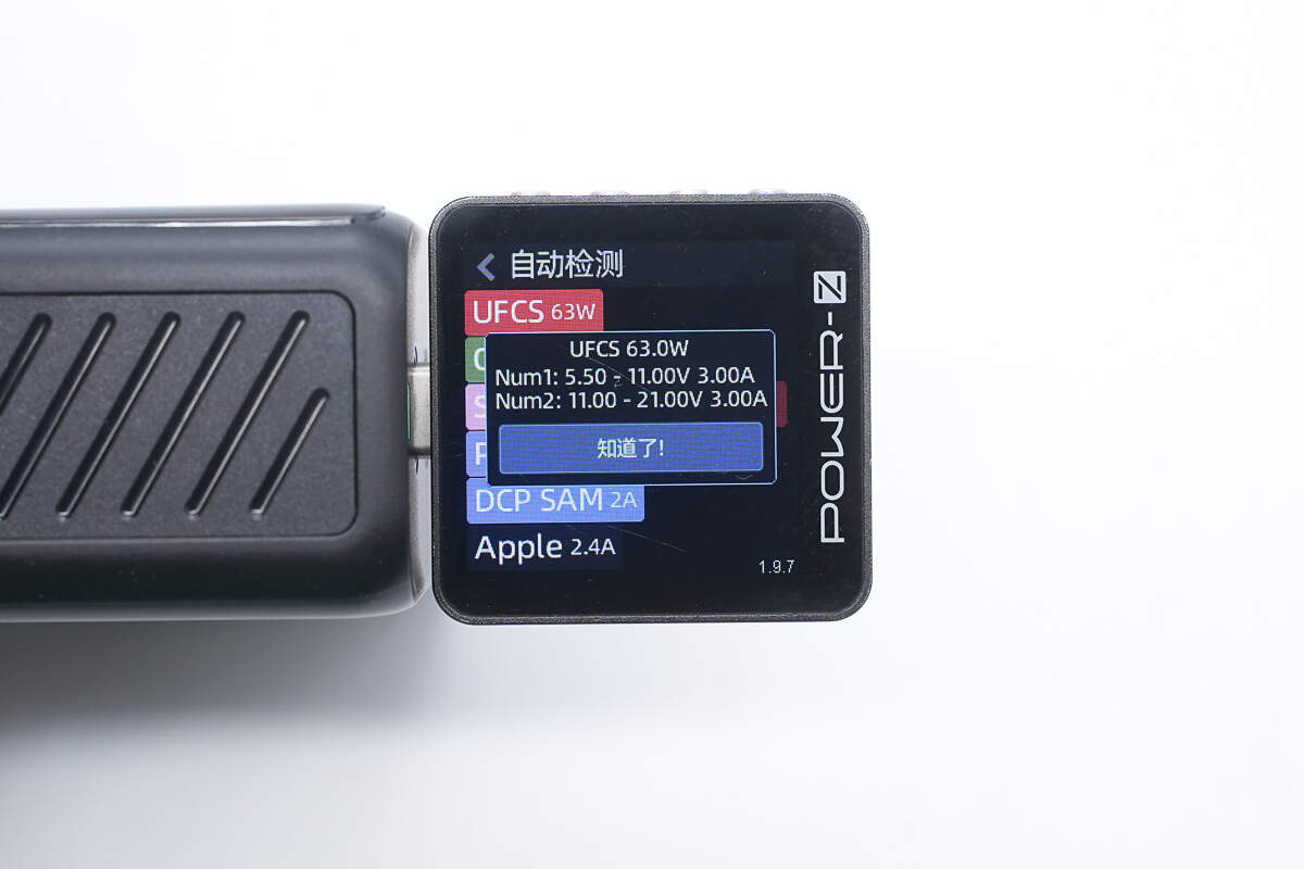
It supports two sets of UFCS voltage ranges: 5.5–11V at 3A and 11–21V at 3A.
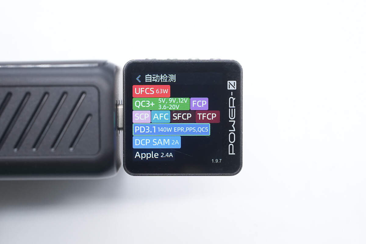
USB-C2 supports the same protocols as USB-C1.
The PDO messages are also identical.
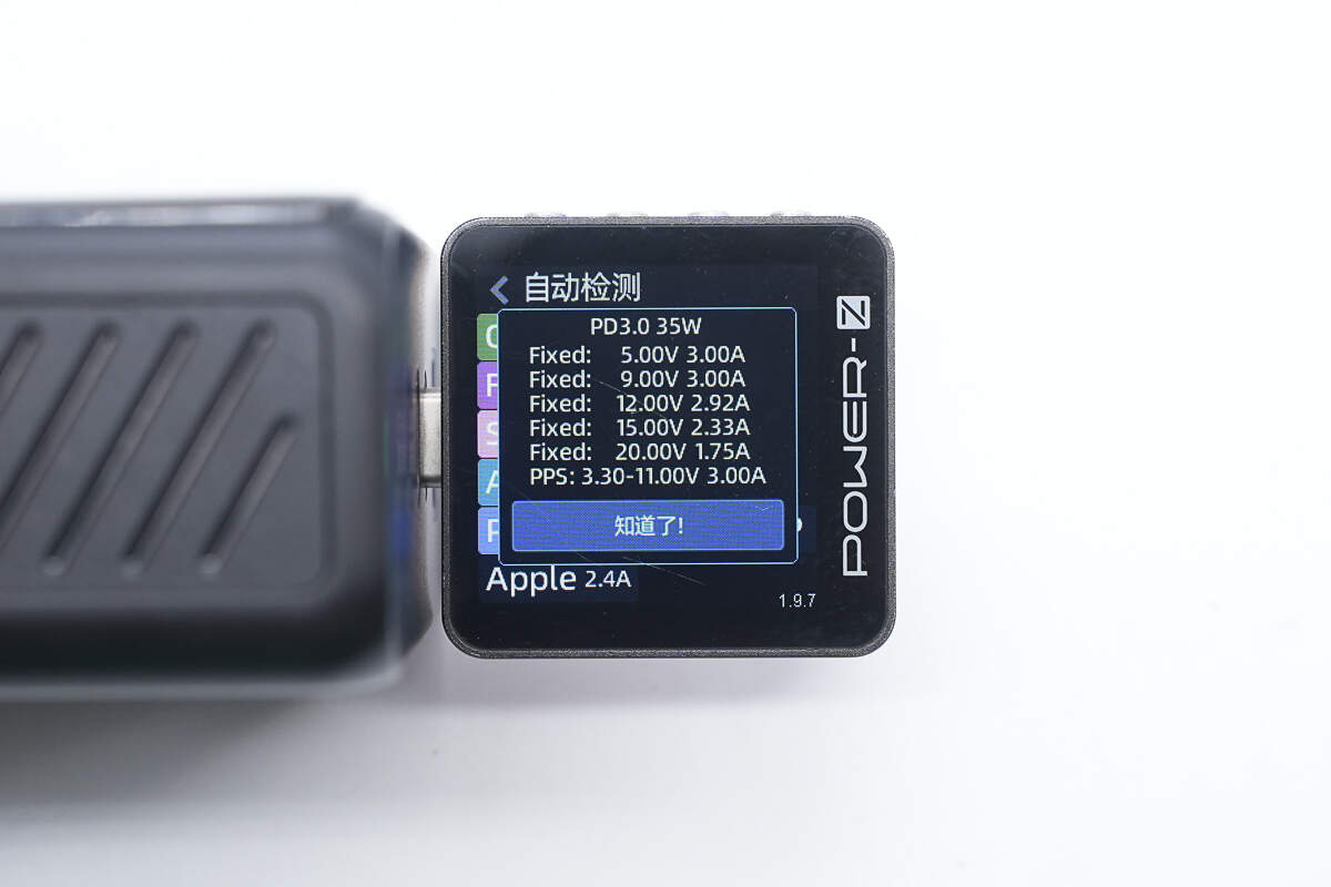
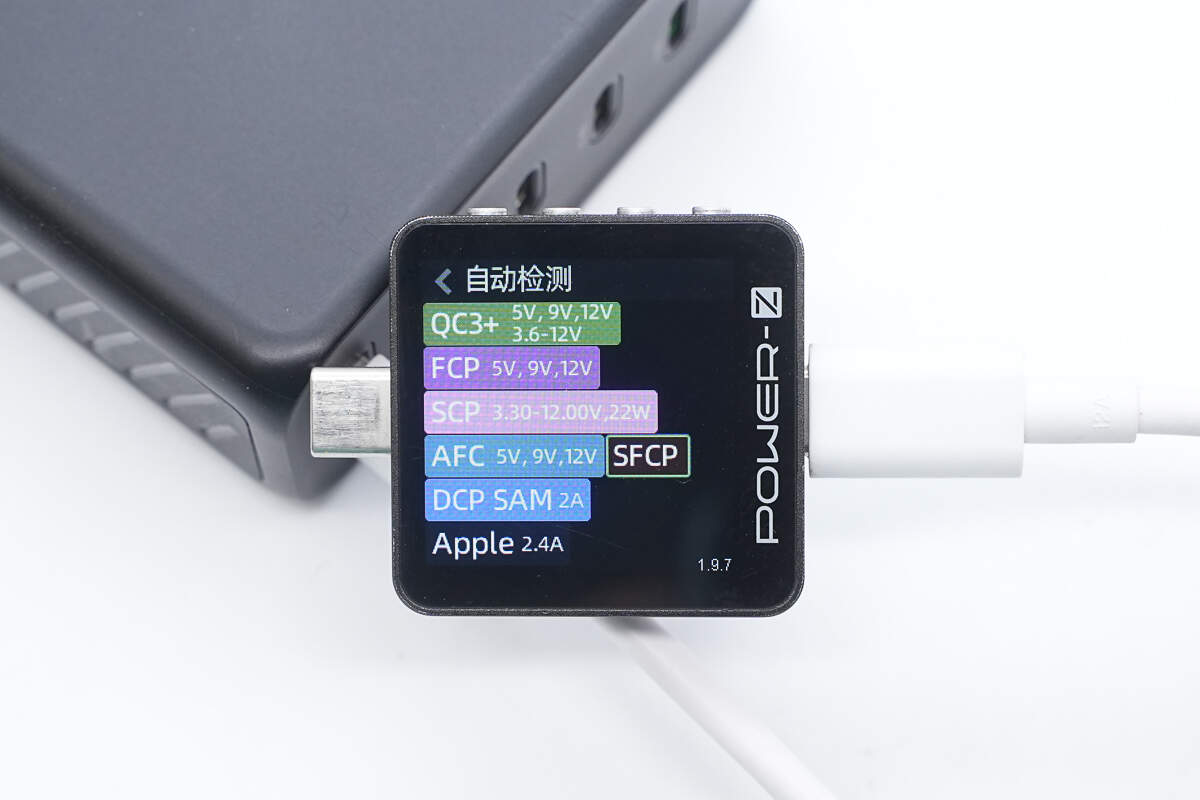
The USB-C3 supports QC3+/4+, FCP, SCP, AFC, SFCP, PD3.0, PPS, DCP, and Apple 2.4A charging protocols.
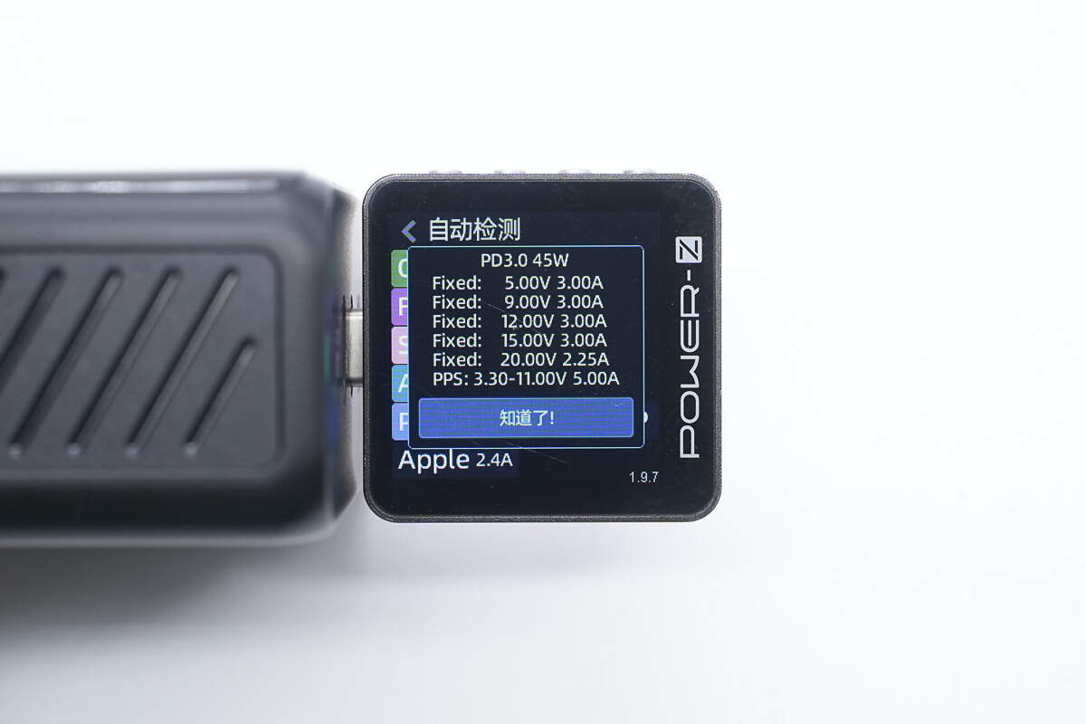
And it has five fixed PDOs of 5V3A, 9V3A, 12V3A, 15V3A, and 20V2.25A, as well as one set of PPS, which is 3.3-11V5A.
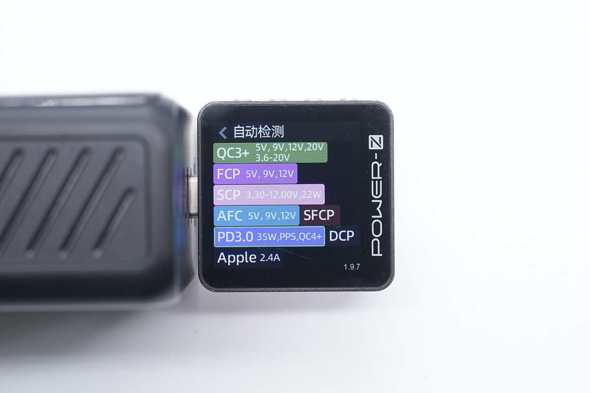
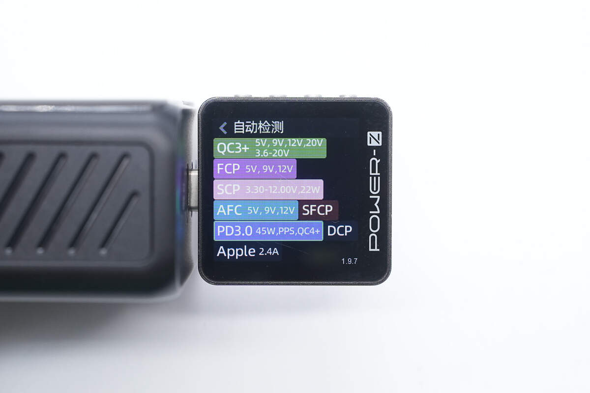
The USB-C4 supports QC3+/4+, FCP, SCP, AFC, SFCP, PD3.0, PPS, DCP, and Apple 2.4A charging protocols.
And it has five fixed PDOs of 5V3A, 9V3A, 12V2.92A, 15V2.33A, and 20V1.75A, as well as one set of PPS, which is 3.3-11V3A.
The USB-A supports QC3+, FCP, SCP, AFC, SFCP, DCP, SAM 2A, and Apple 2.4A charging protocols.
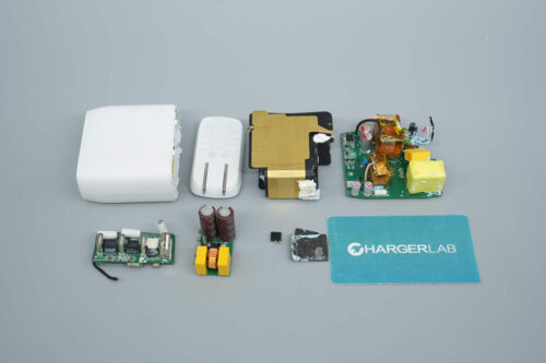
Teardown
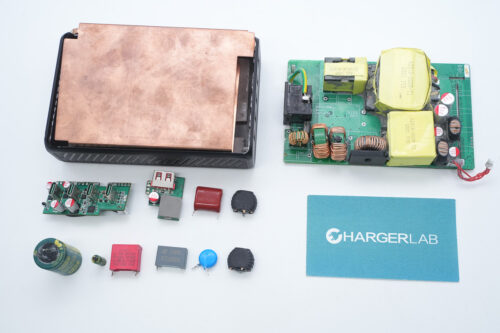
Next, let's take it apart to see its internal components and structure.
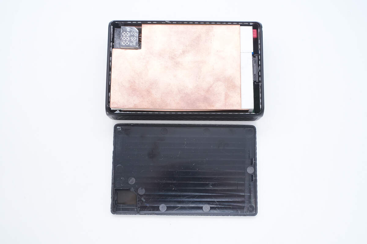
Open the casing, which uses ultrasonic welding.
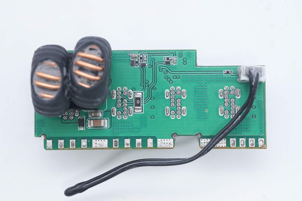
The PCBA module is connected to the screen via a plug-in wire connection.
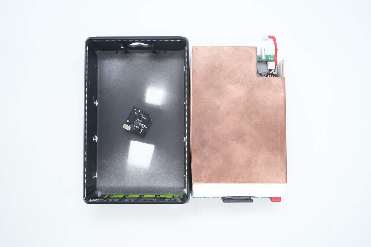
Separate the PCBA module from both the casing and the screen.
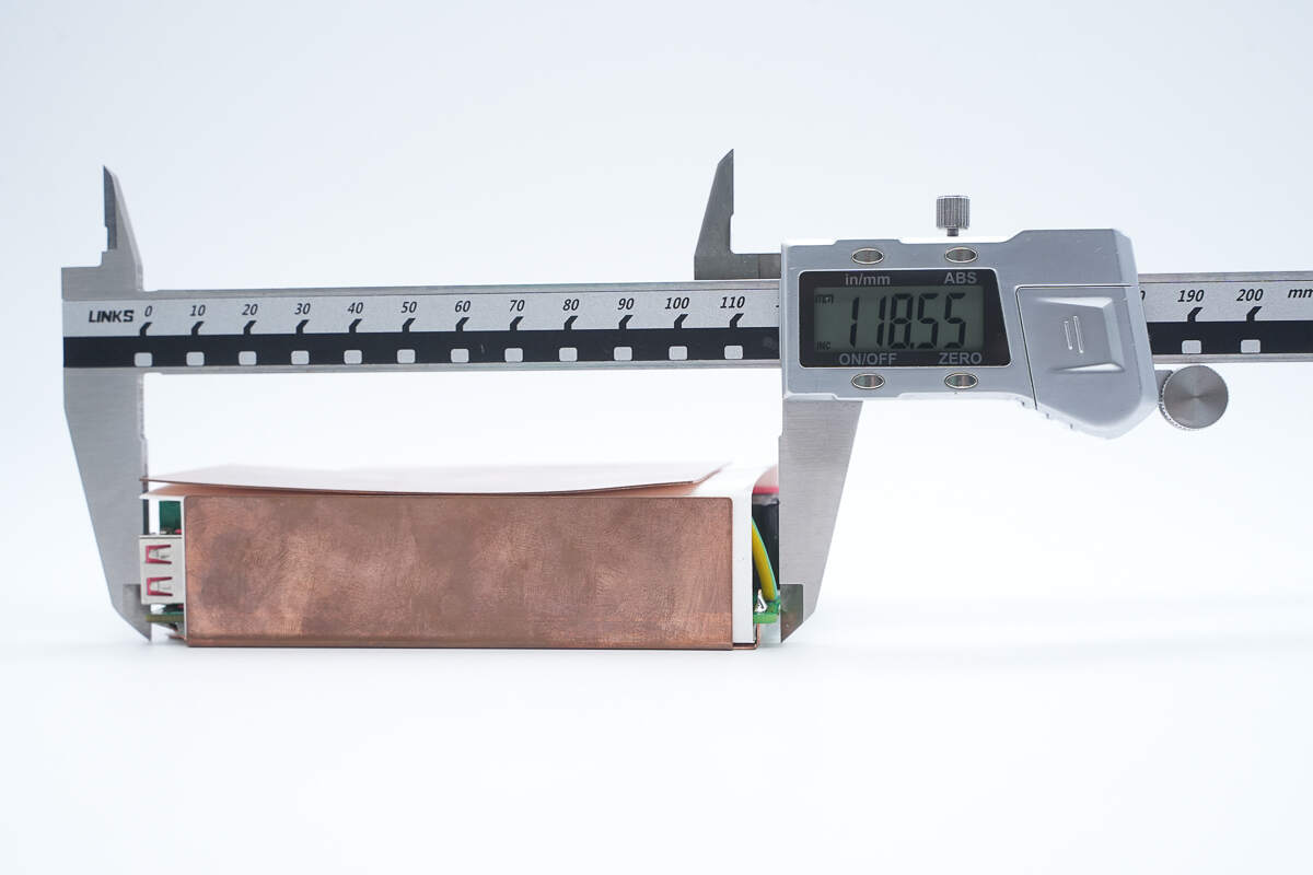
The length of the PCBA module is about 118.55 mm (4.67 inches).
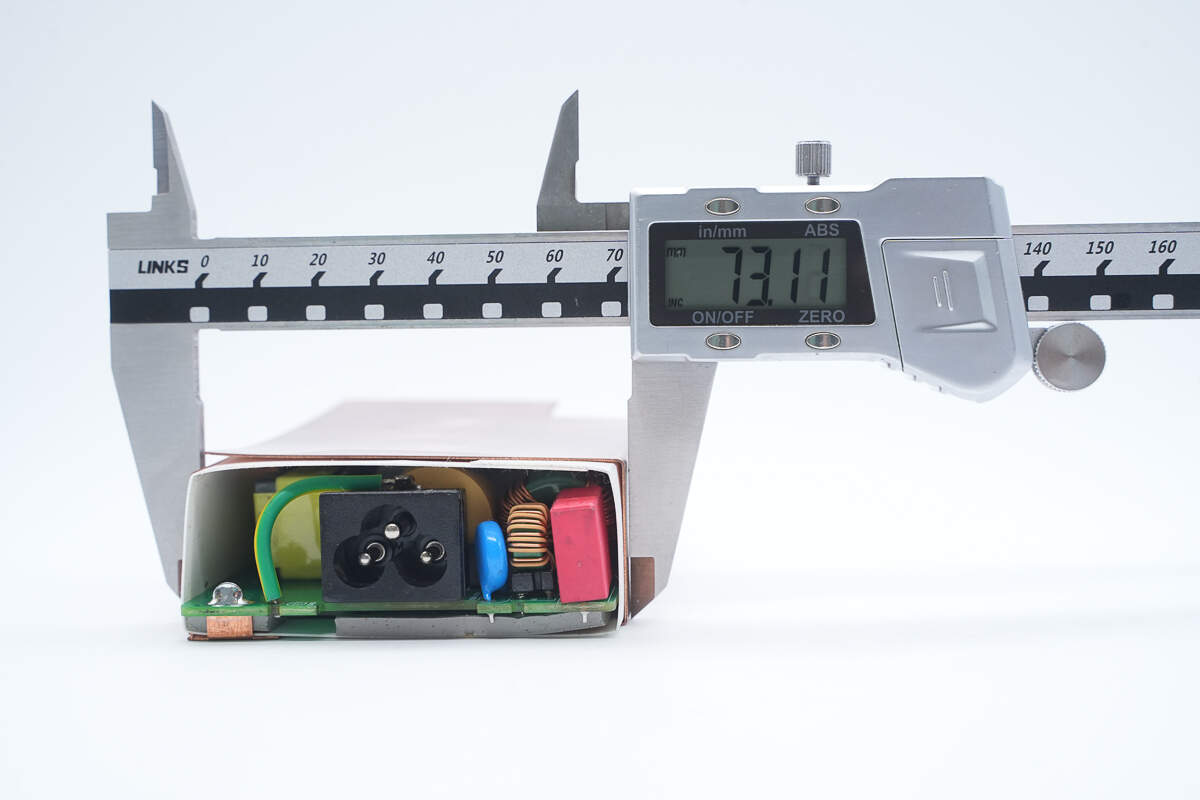
The width is about 73.11 mm (2.88 inches).
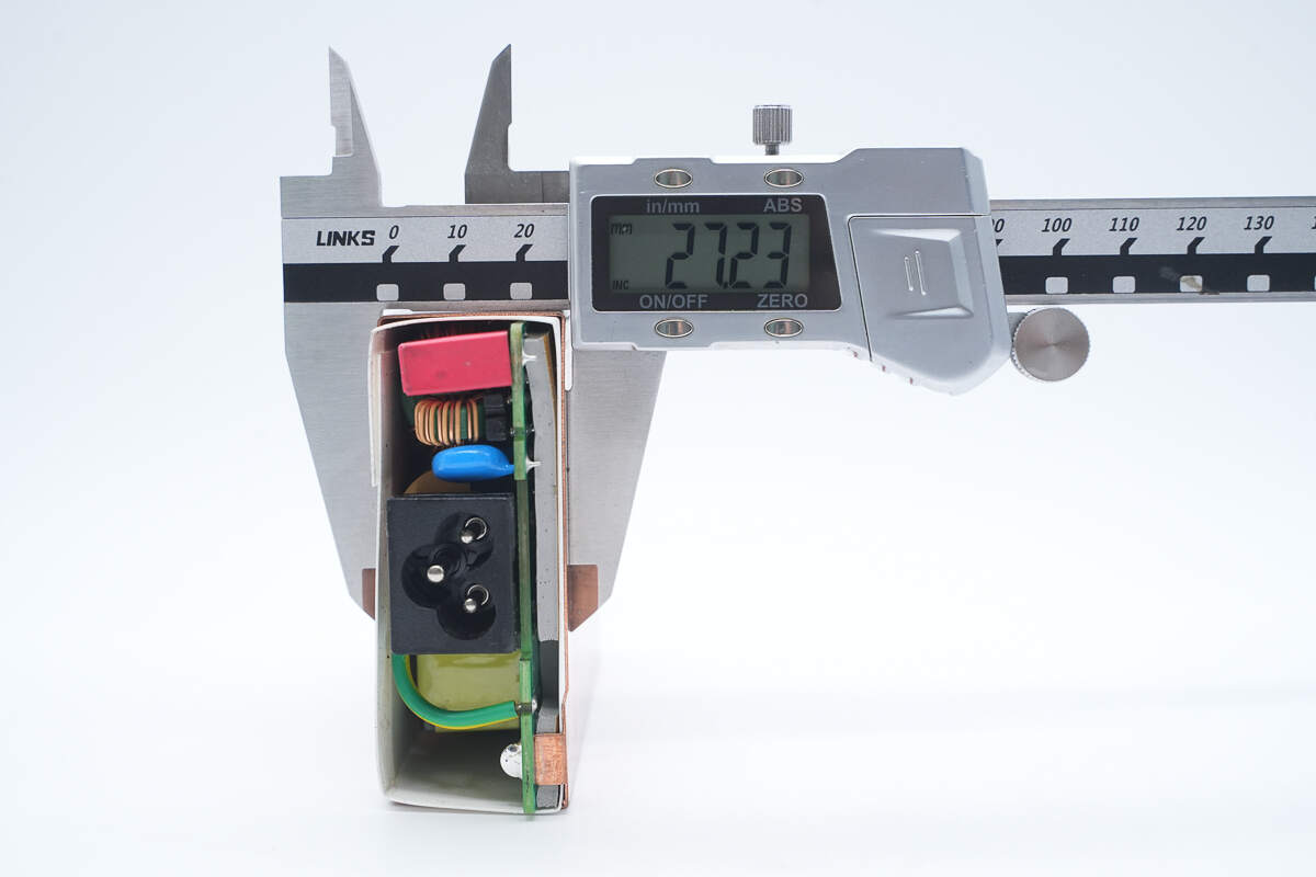
The thickness is about 27.23 mm (1.072 inches).
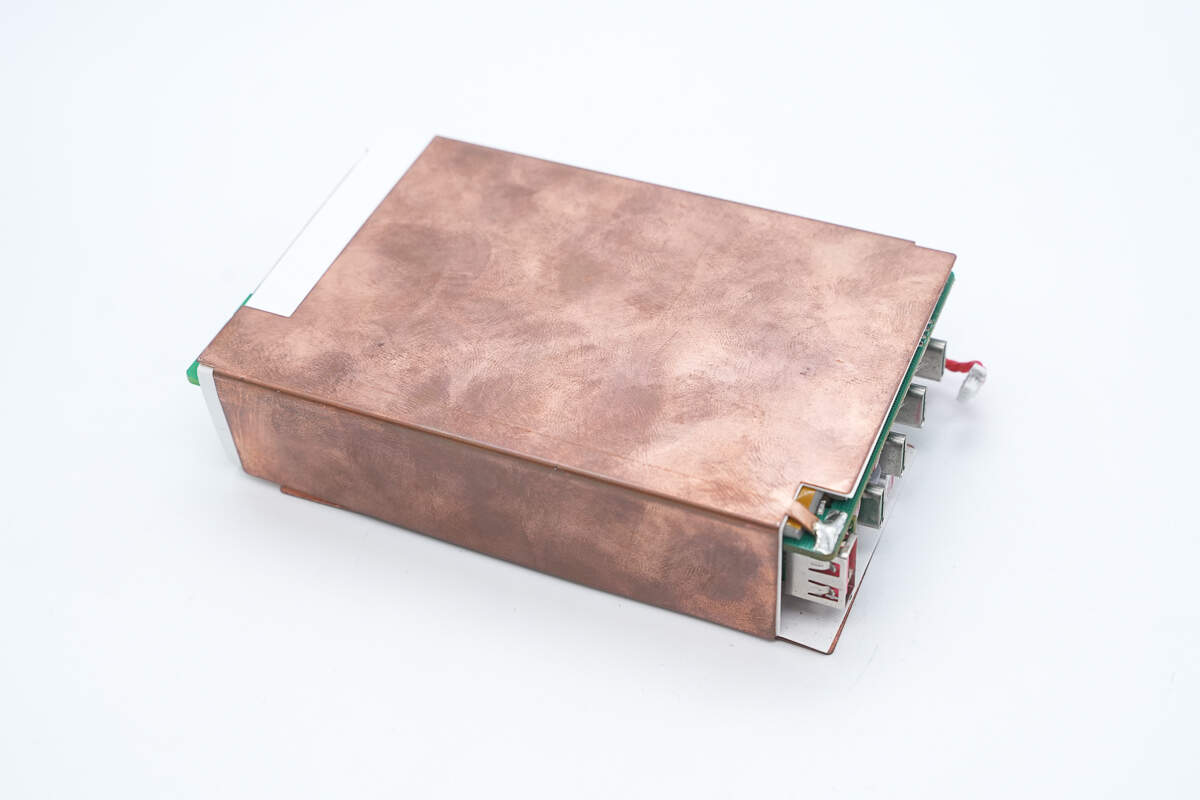
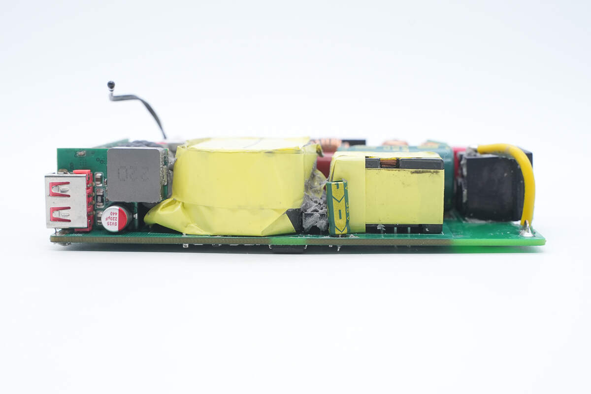
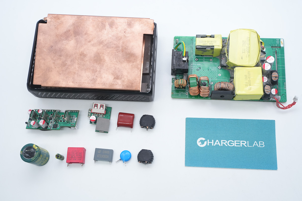
The PCBA module is enclosed in an integrated copper heatsink, which is soldered in place for fixation.
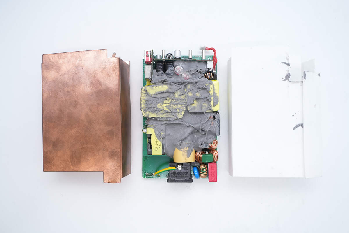
After removing the heatsink, a white plastic insulation plate is found on the inner side.
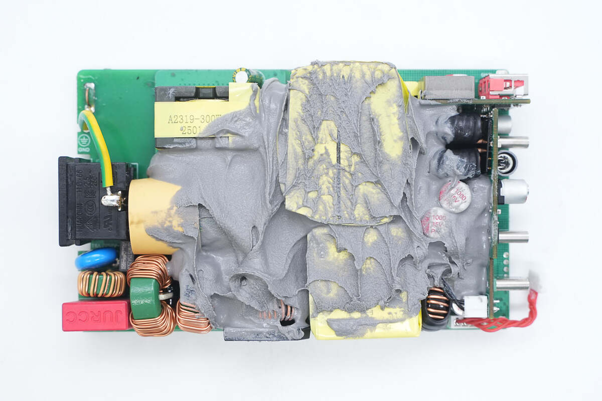
The gaps between components on the front side of the PCBA module are filled with thermal gel.
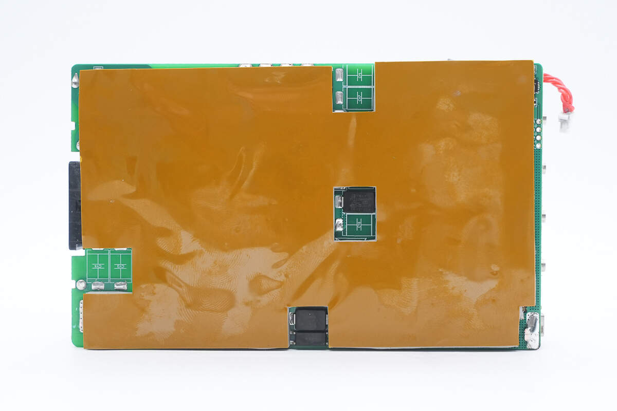
The back side is covered with a thermal pad.
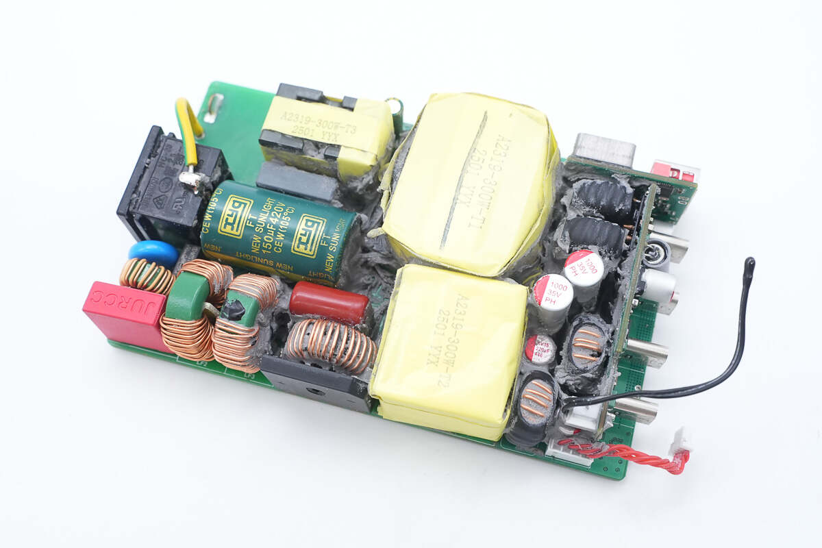
Clean off the thermal gel. On the front side, there are components such as a fuse, common mode choke, rectifier bridge, PFC boost inductor, transformer, and others.
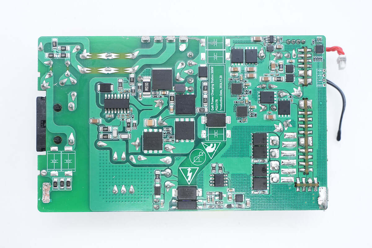
On the back side, there are components including the master control chip, PFC boost MOSFET, PFC rectifier, LLC MOSFET, synchronous rectifier controller, synchronous rectifier, buck protocol chips for two secondary buck circuits, synchronous buck MOSFETs, and other related components.
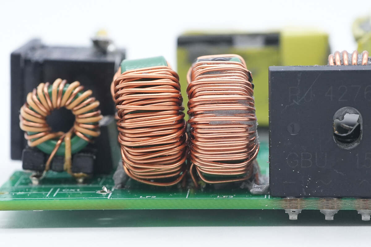
Input side overview: The ground wire of the cloverleaf connector is soldered to the PCB via a wire. On the right side, there is a time-delay fuse, a varistor, a common mode choke, and a safety X2 capacitor.
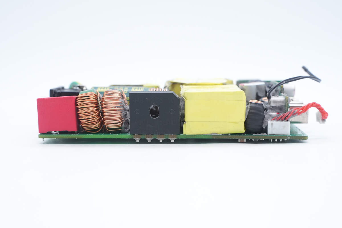
On the side, there are two additional common mode chokes, a bridge rectifier, and a PFC boost inductor.
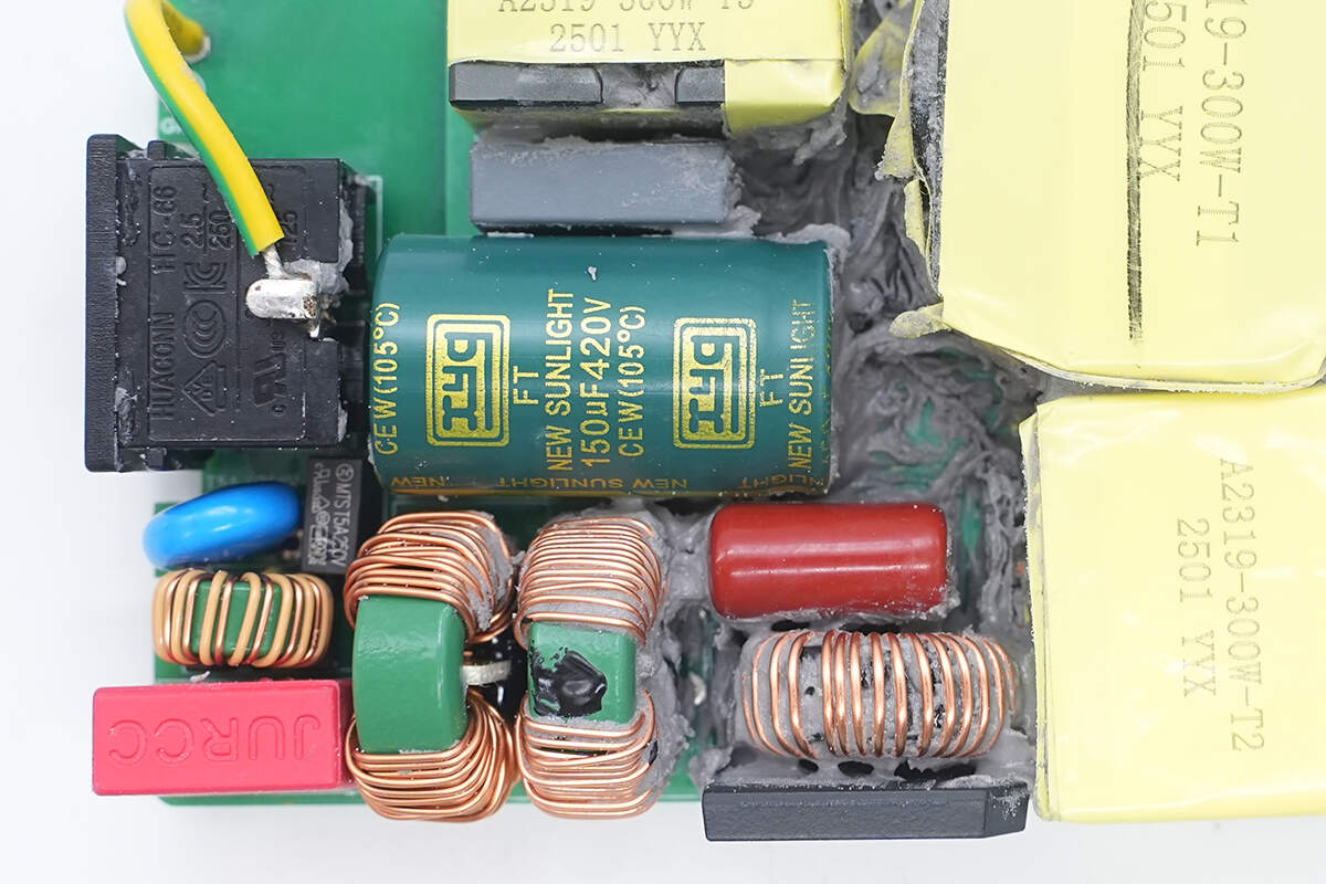
In the central area, there are a filter inductor, a film capacitor, an electrolytic capacitor, and a resonant capacitor.
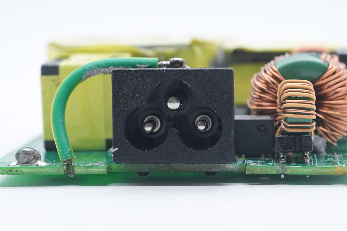
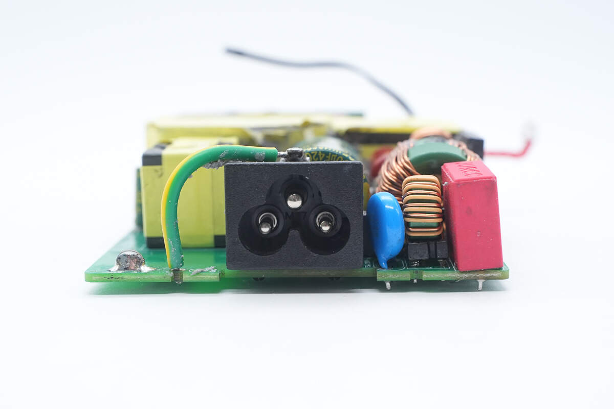
Close-up of the input socket.
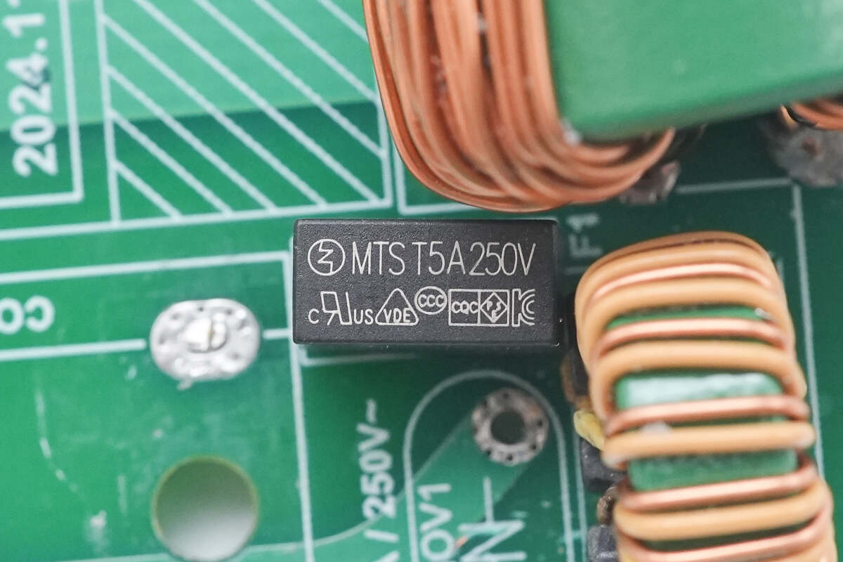
The time-delay fuse is rated at 5A 250V.
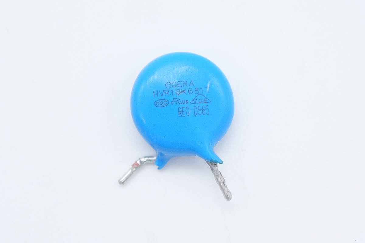
The HVR10K681 varistor is used for surge overvoltage protection.
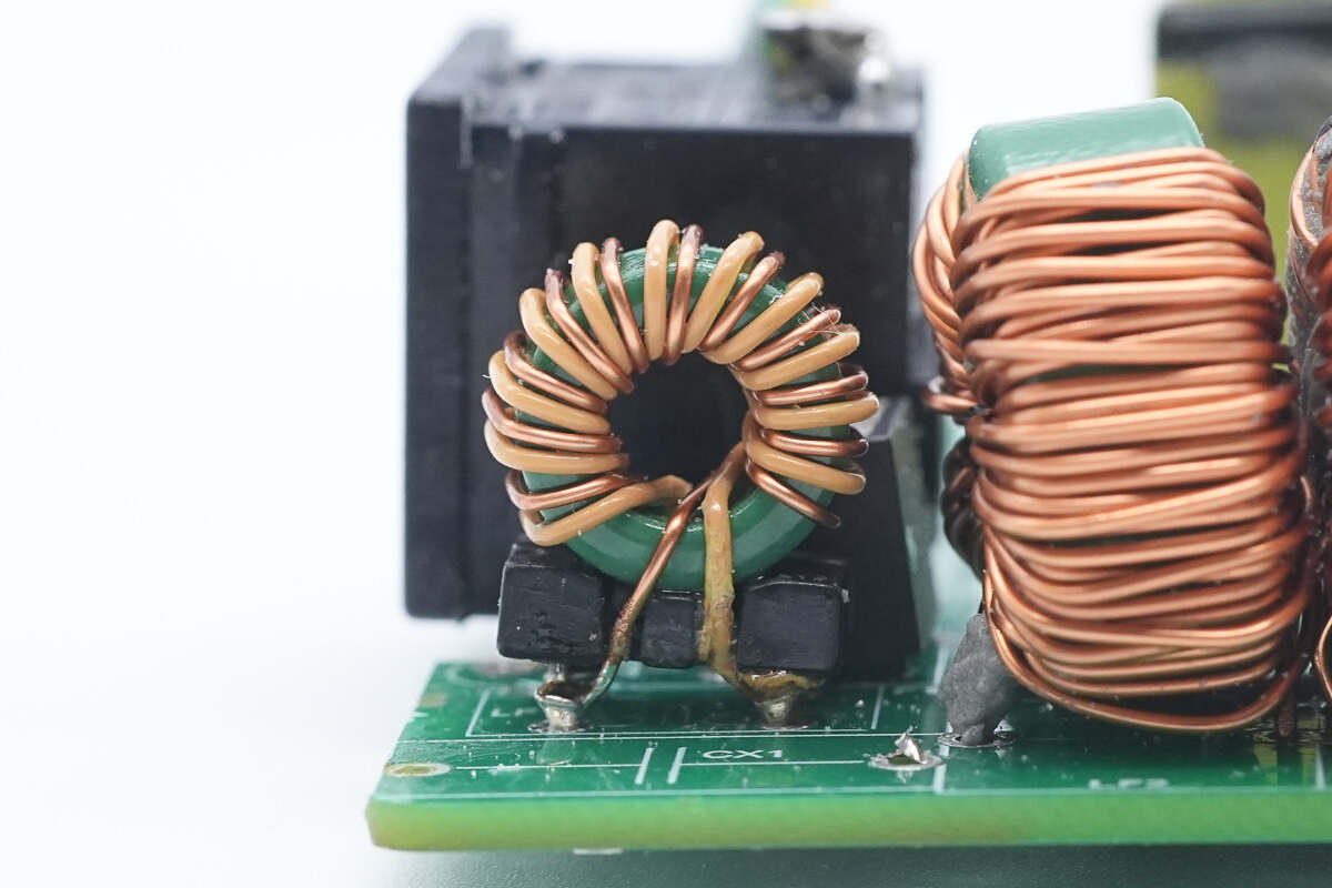
The three-stage design of the common mode chokes helps to better filter out EMI interference. The first choke uses a bifilar winding.
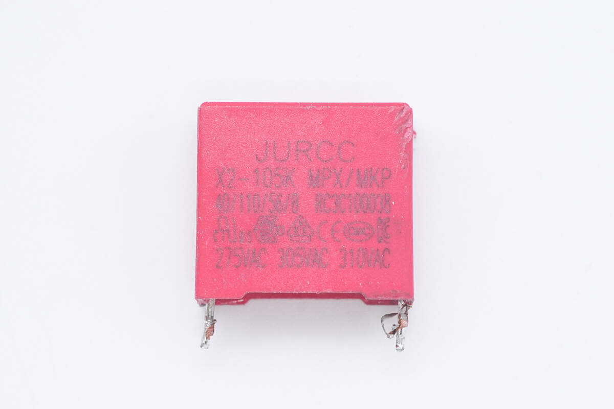
The safety X2 capacitor is from JURCC. 1μF.
Close-up of the other two common mode chokes.

The bridge rectifier is from PANJIT, model GBU1506ULV, rated at 600V 15A, and uses a GBU-2 package.
Close-up of the filter inductor.
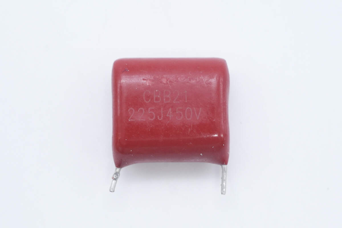
The CBB21 film capacitor is rated at 2.2 μF, 450V.
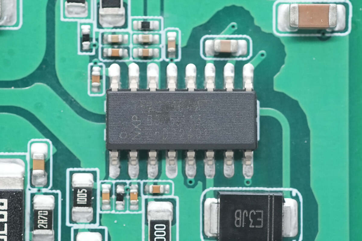
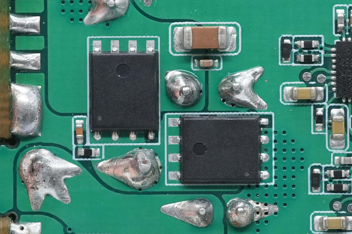
The primary control chip is the NXP TEA2016AAT, which integrates both an LLC controller and a PFC controller. It features a digital architecture that simplifies design and reduces the number of external components. The chip includes multiple comprehensive protection features, offers a high level of integration, and comes in an SO16 package.
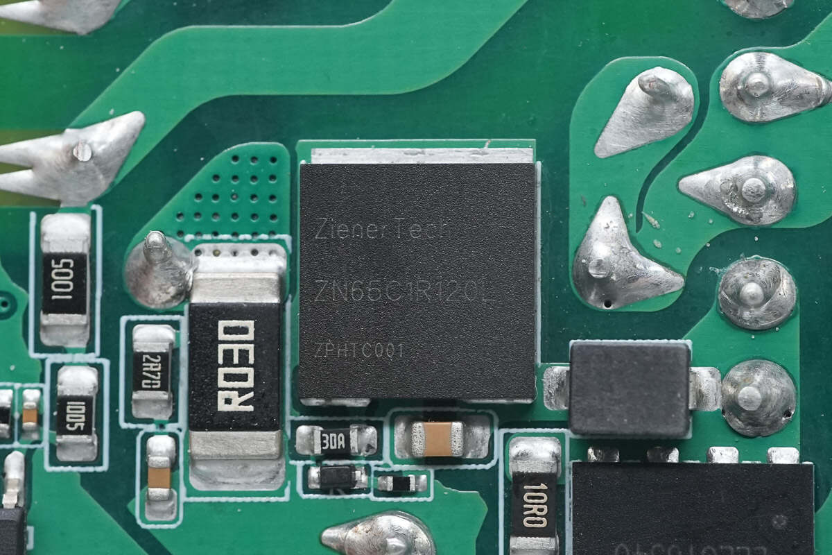
The PFC MOSFET is from ZIENER, model ZN65C1R120L. It is a GaN power device rated at 650V with an on-resistance of 120 mΩ and comes in a DFN8×8 package.
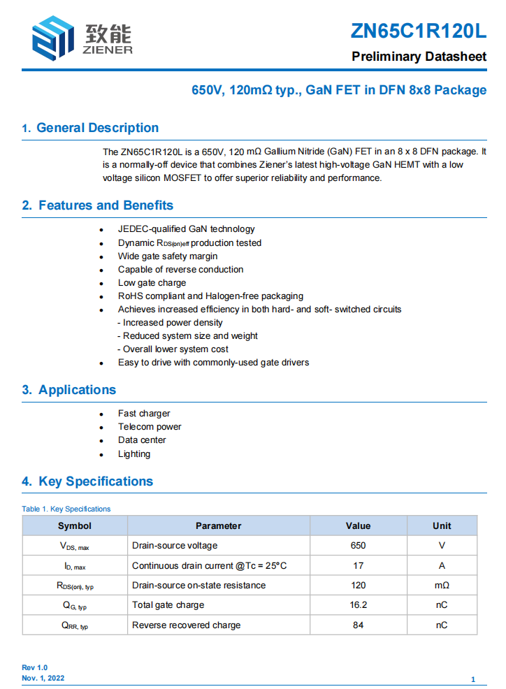
Here is the information about ZIENER ZN65C1R120L.
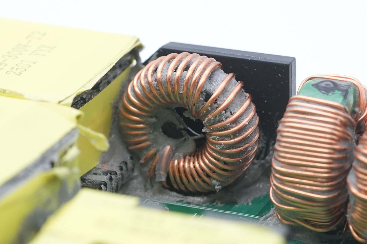
Close-up of the PFC boost inductor.
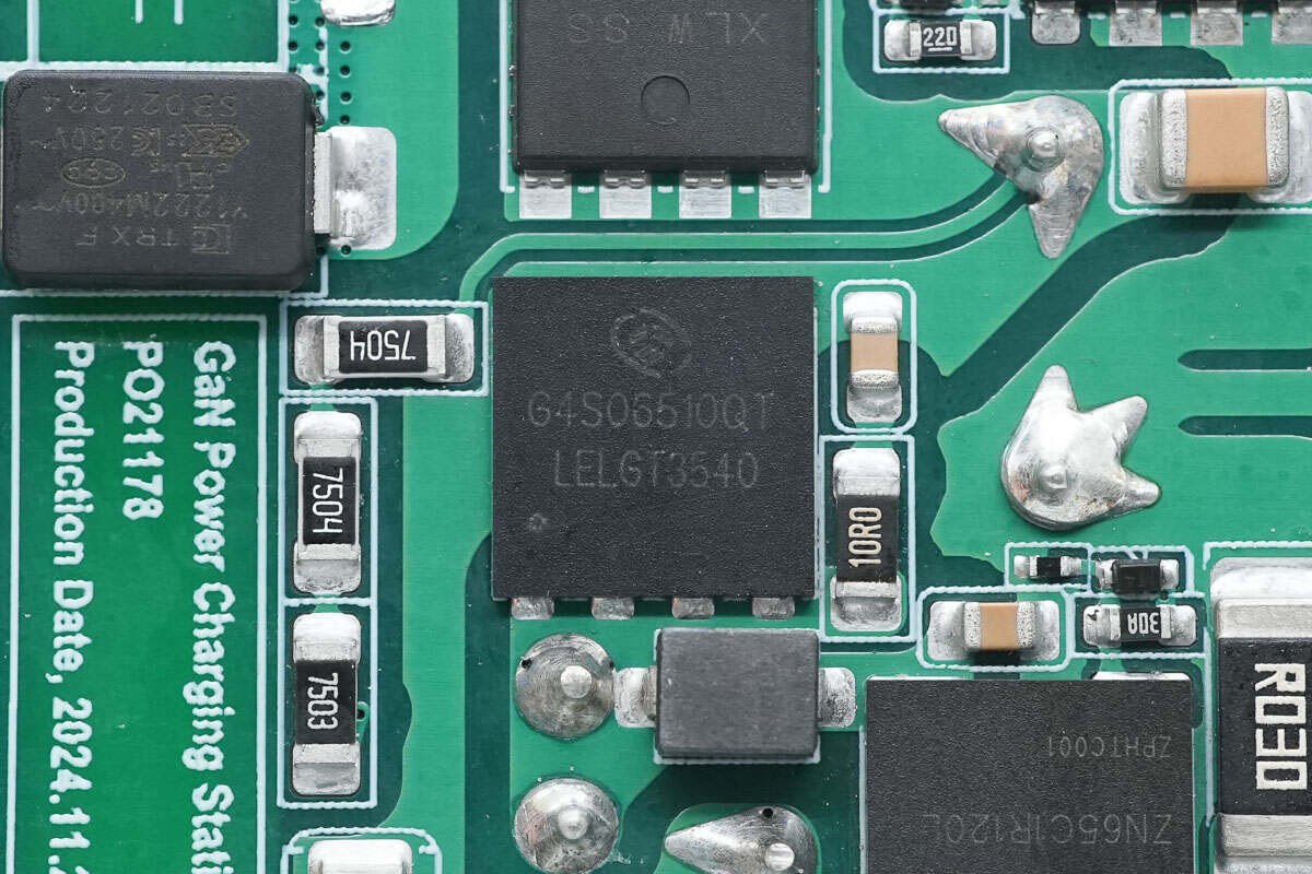
The PFC rectifier is from GPT, model G4S06510QT. It is a silicon carbide (SiC) Schottky diode rated at 650V and 10A, housed in a DFN8×8 package.
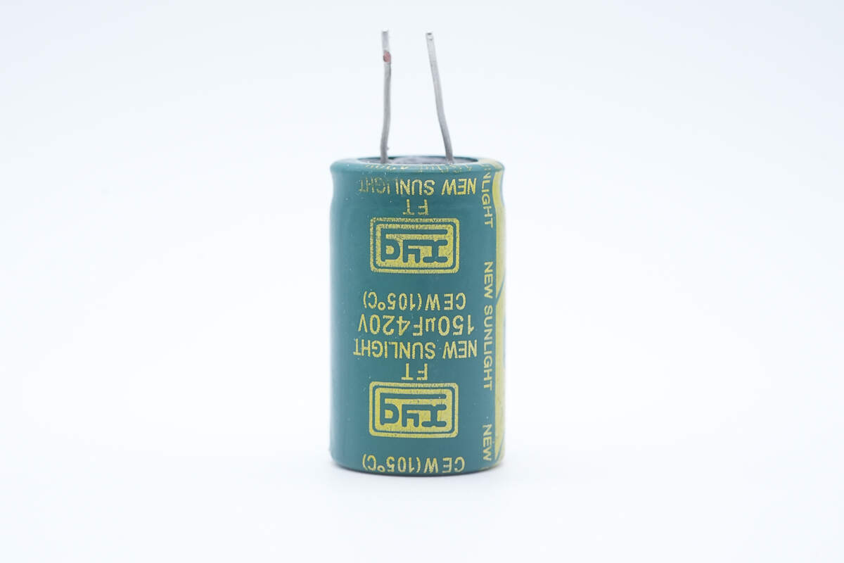
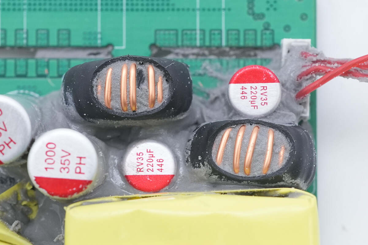
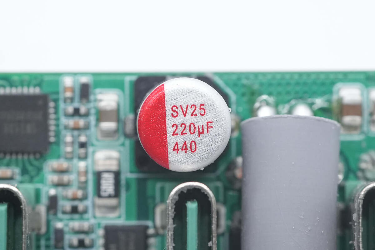
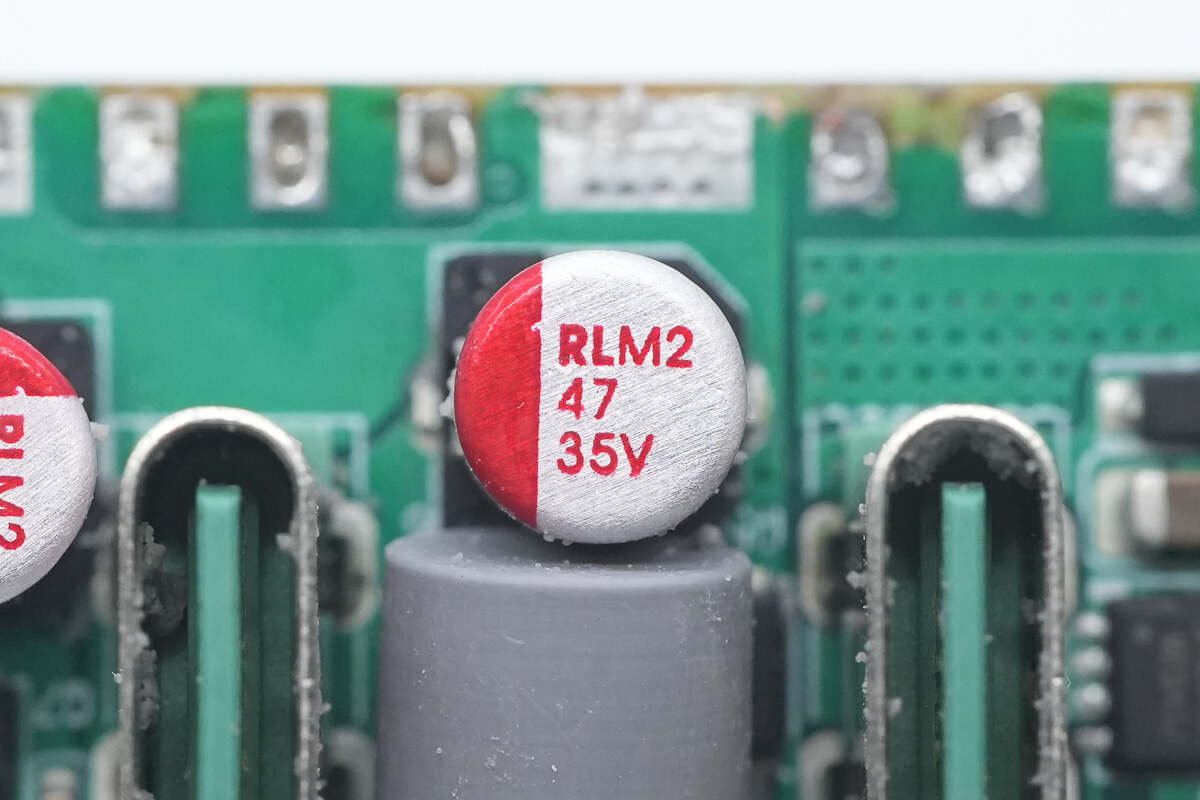
The electrolytic capacitor is rated at 420V, 150μF.
On the other side, there is a resonant inductor, a capacitor for powering the master control chip, and a transformer.
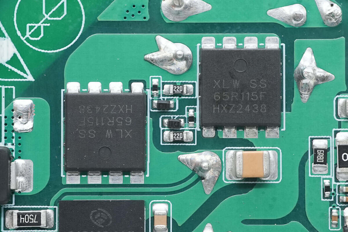
The LLC MOSFETs are from XLW, marked with 65R115F, and come in a PDFN8×8 package.
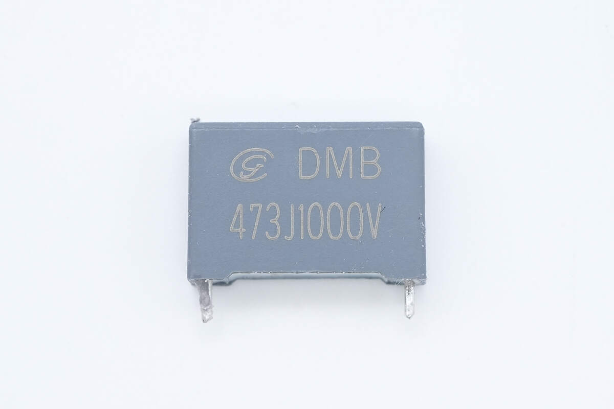
The resonant capacitor is rated at 0.047 μF, 1000V.
Close-up of the resonant inductor.
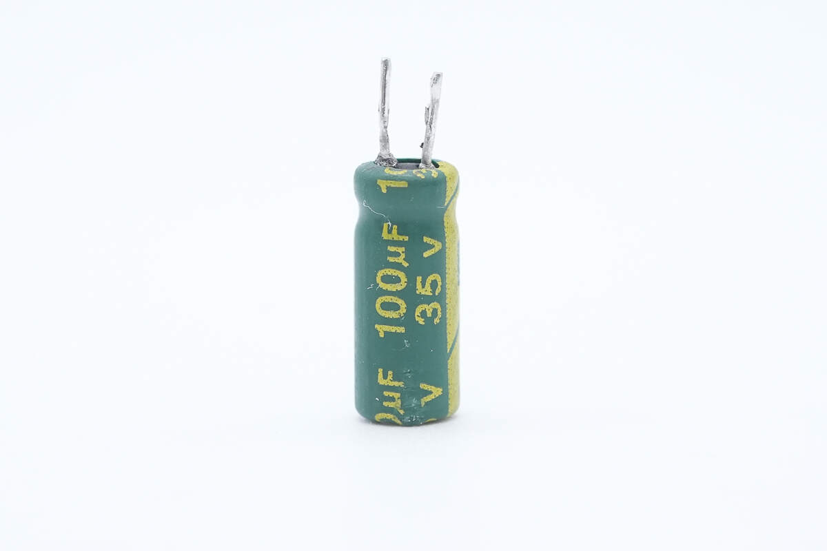
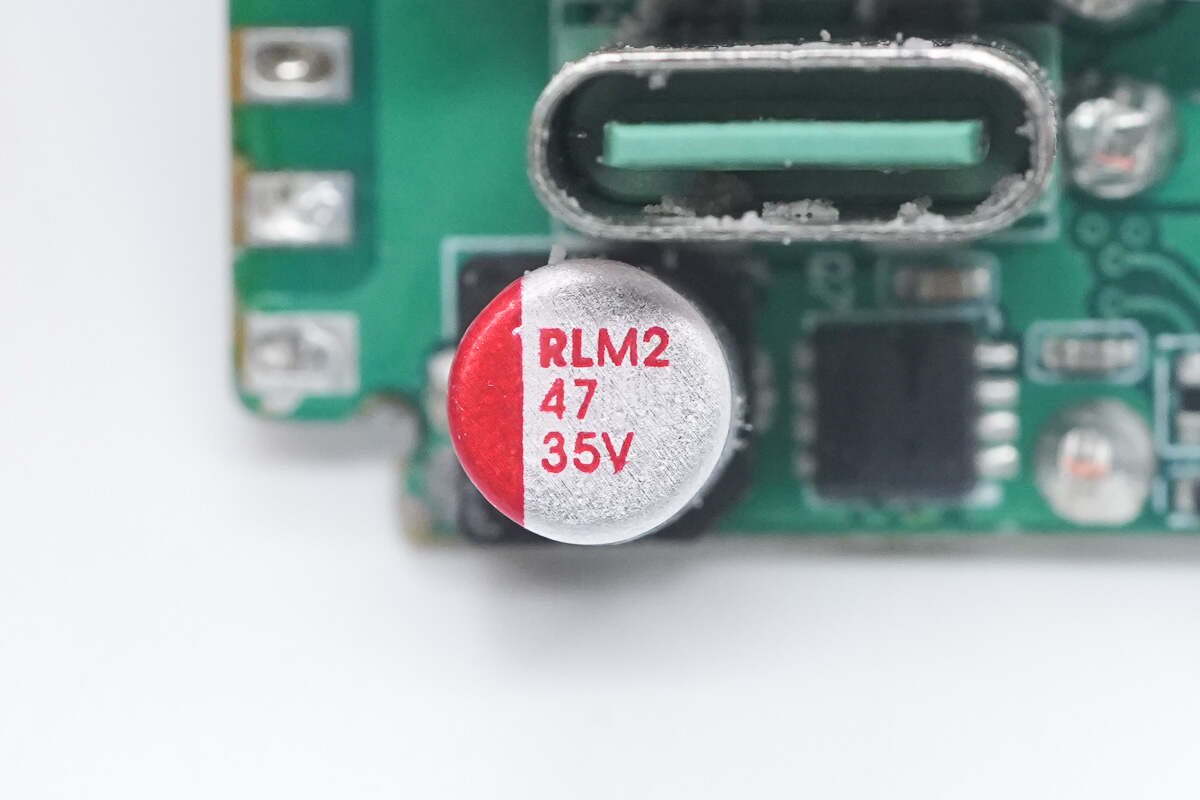
The capacitor used to power the master control chip is rated at 35V, 100μF.

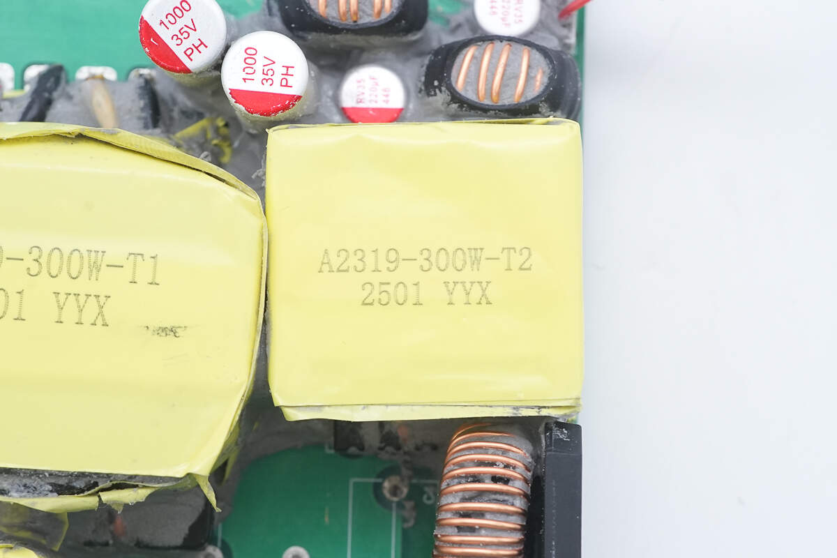
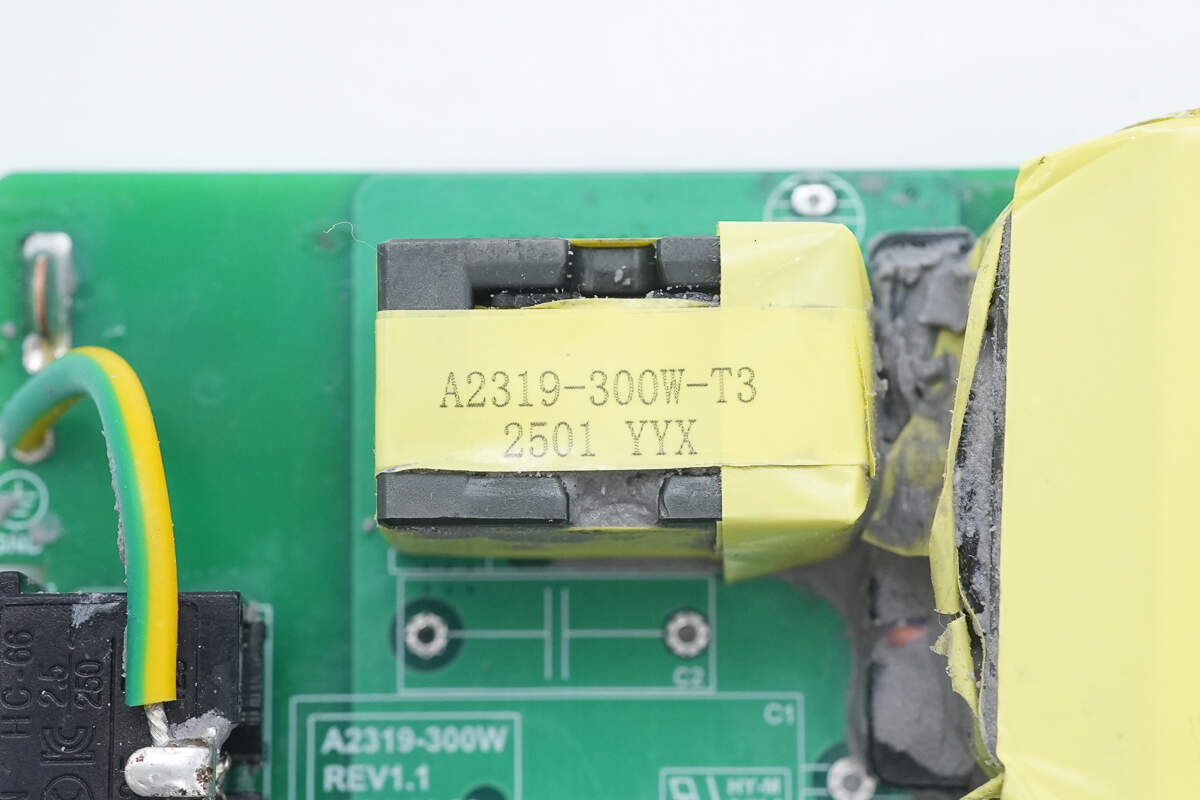
Close-up of the transformer.
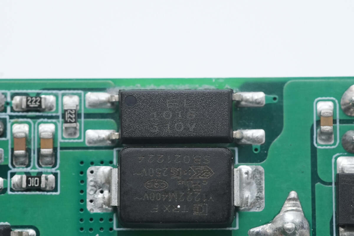
The Everlight EL1018 optocoupler is used for output voltage feedback.
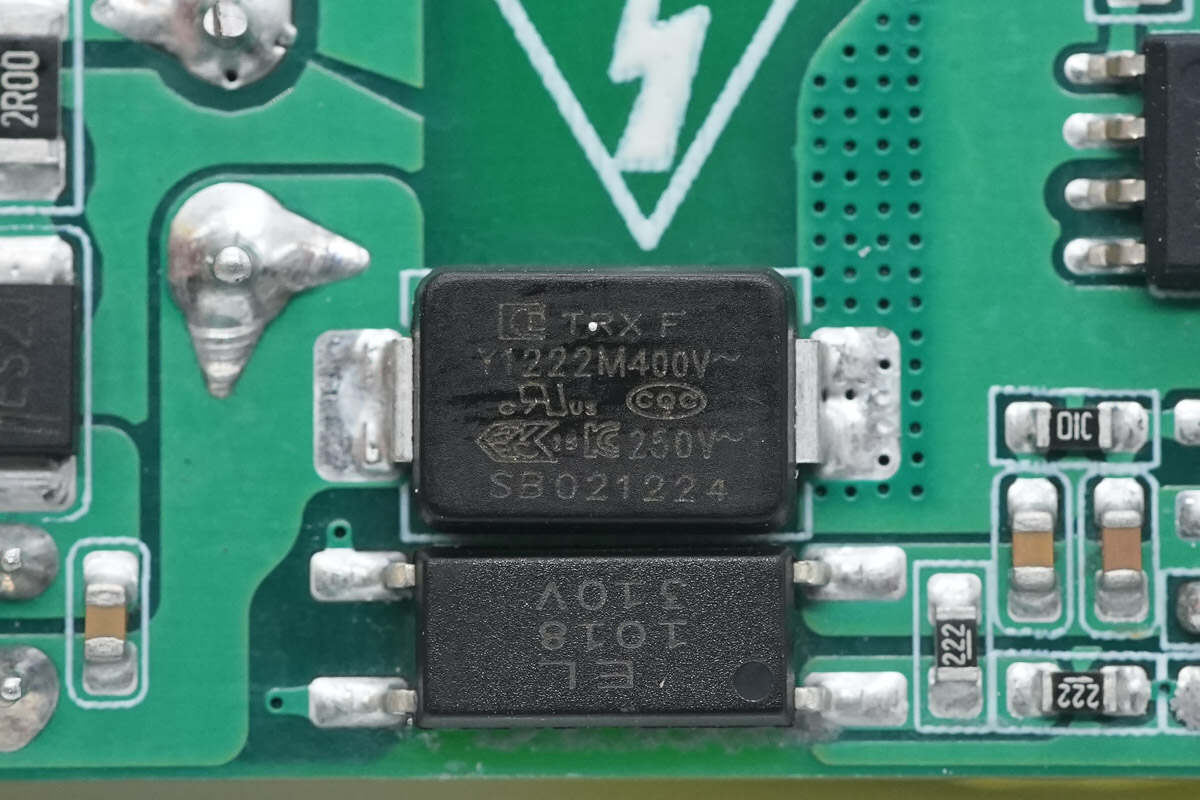
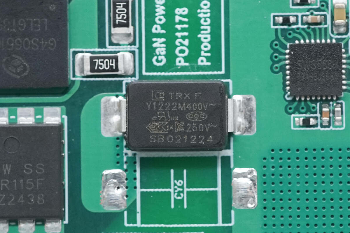
The SMD Y capacitor is from TRX. Its small size and light weight are suitable for high-density power products such as GaN fast chargers. The part number is TMY1222M.
Close-up of the other TRX TMY1222M SMD Y capacitor.
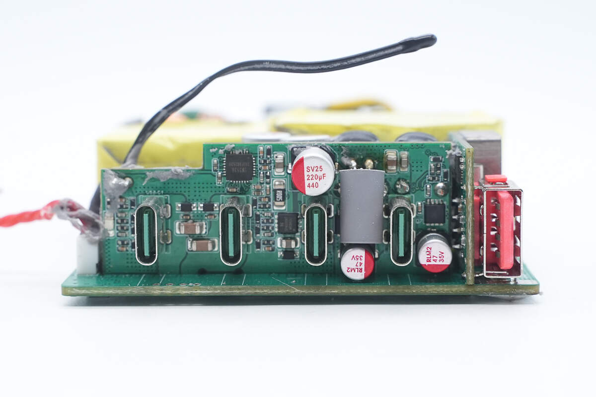
At the output end, there are small PCBs with connector sockets.

After removing the PCBs, previously hidden components are revealed, including solid capacitors and buck inductors.
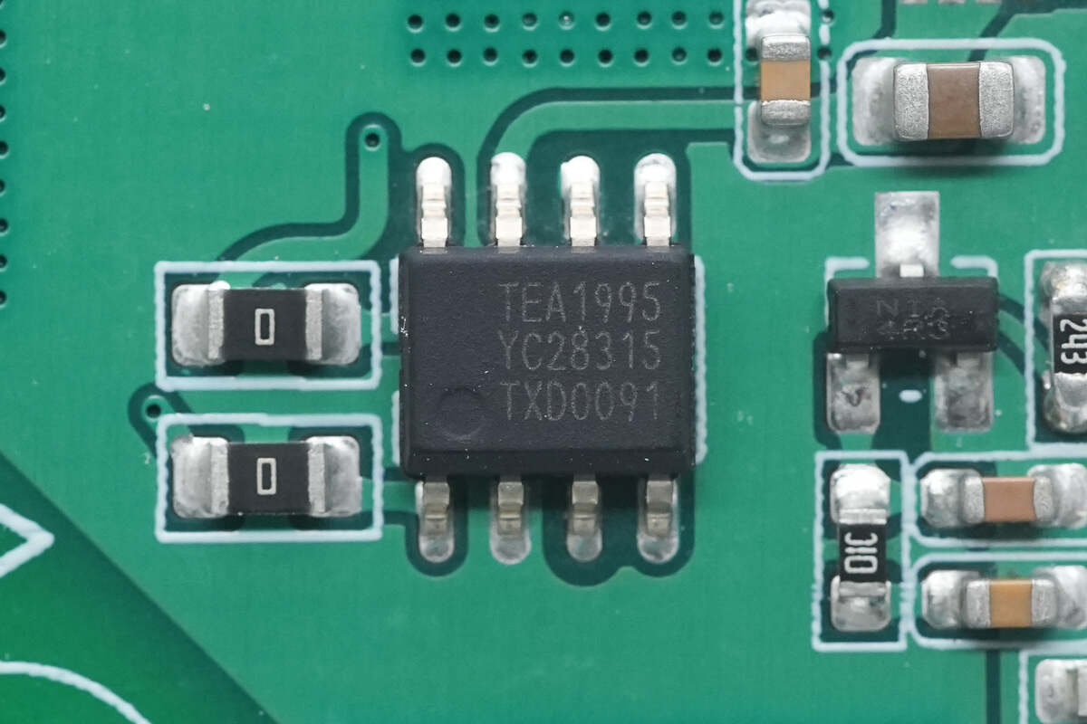
The synchronous rectifier controller is from NXP, model TEA1995. It integrates two independent synchronous rectifier drivers designed for LLC topology power supplies. It features a simplified external component design, supports an operating voltage of up to 38V, and is capable of handling 28V output for USB PD 3.1 compliance.
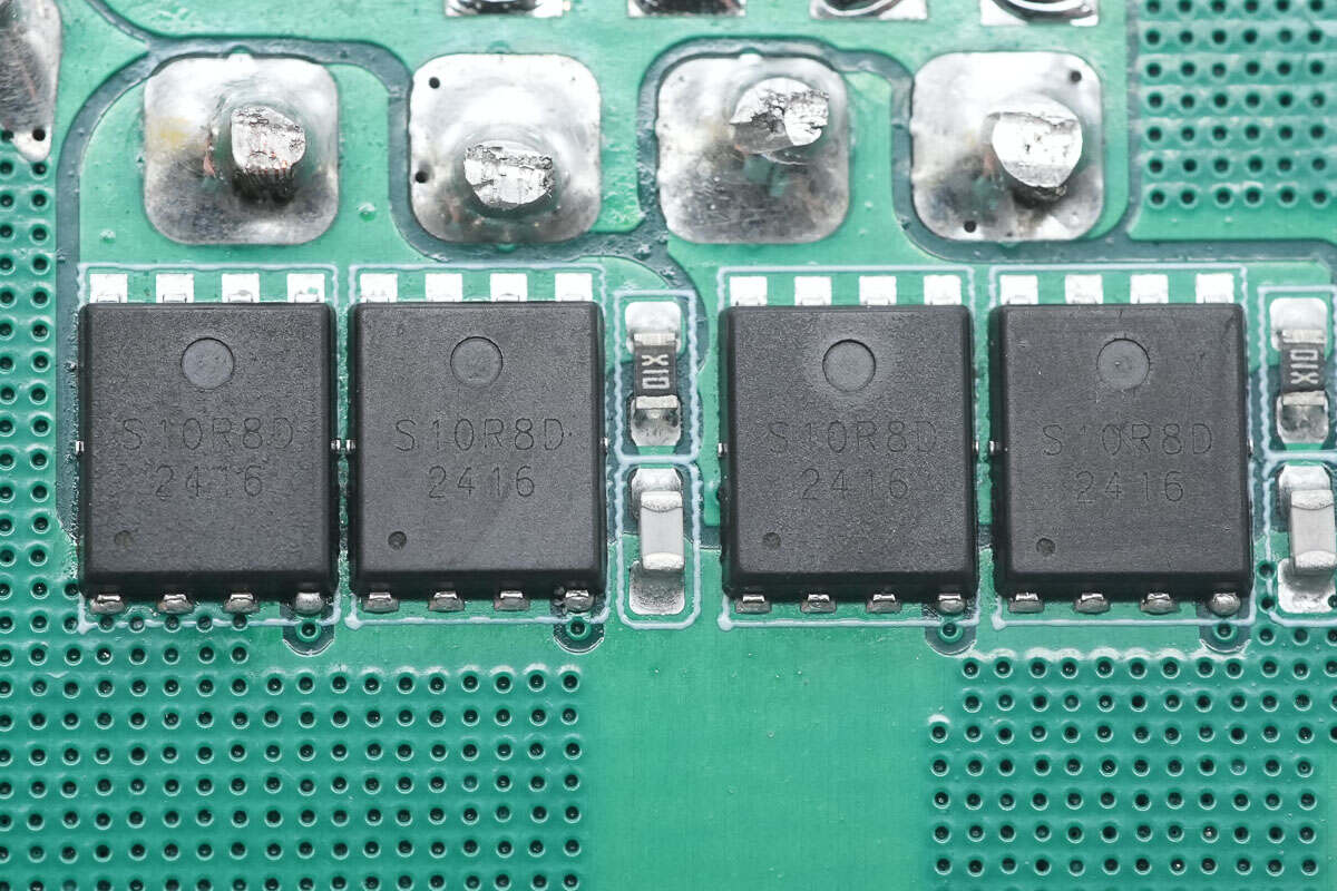
The four synchronous rectifiers are marked with S10R8D.
There is one unmarked MOSFET with no identifiable markings, so its specifications are unknown.
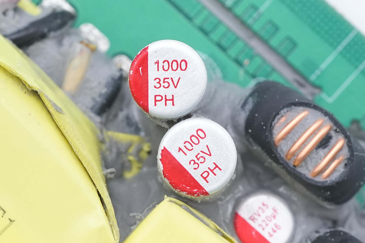
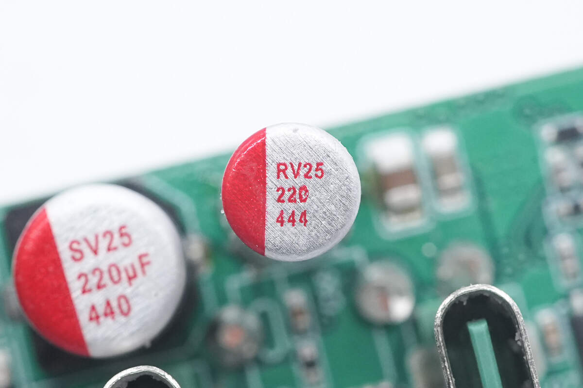
The two solid capacitors used for output filtering are both rated at 35V, 1000μF.
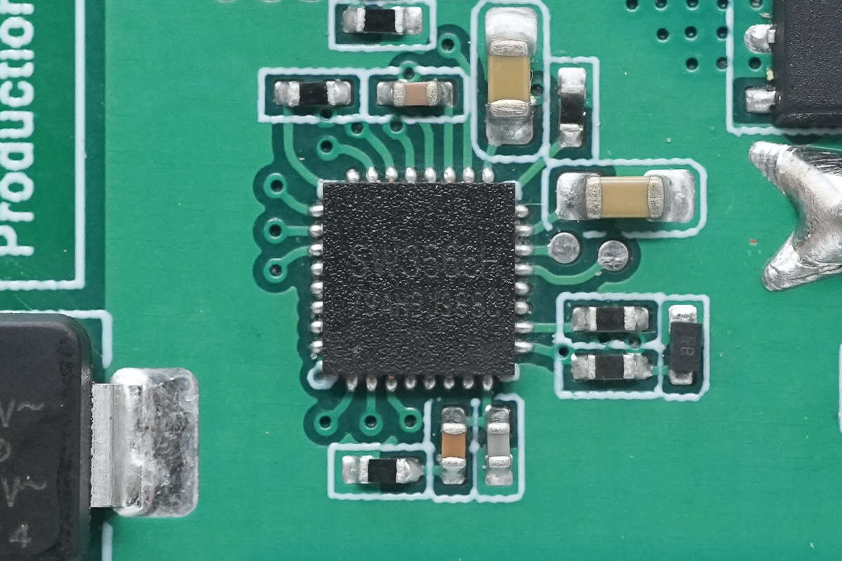
The USB-C1 port uses the iSmartWare SW3566H as its buck protocol chip. This is a highly integrated dual-port fast-charging SoC that supports both USB-C and USB-A ports with independent current limiting. It includes a high-efficiency synchronous buck converter and supports fast charging protocols such as PD3.1, QC, SCP, and UFCS, with customizable protocol options. It supports outputs up to 20V/7A and 28V/5A, with a maximum output power of 140W.
SW3566H integrates CC/CV control, dual-port management logic, and bus voltage monitoring. Paired with suitable buck and VBUS MOSFETs, it enables dual-port buck output. The internal buck converter operates at 180kHz and supports both PWM and PFM modes. Output current, line loss compensation, and protection thresholds can be configured via the I²C interface. It's built-in ADC monitors input/output voltage, output current, chip temperature, and more (up to 9 channels), and it can interface with an external MCU for parameter display.
It supports up to 36V input and 7A output, with comprehensive protections including soft start, input/output OVP/UVP, OCP, SCP, DP/DM/CC OVP, overtemperature protection, external NTC support, and power limiting. The chip comes in a QFN4×4-32 package.
Here is the information about iSmartWare SW3566.
Close-up of the two synchronous buck MOSFETs used in conjunction with the SW3566H.

The USB-C2 port also uses the iSmartWare SW3566H as its buck protocol chip.
The two synchronous buck MOSFETs paired with the USB-C2 port are unmarked, and their specifications are unknown.
The buck inductors for both buck circuits are covered with heat shrink tubing for insulation. The solid capacitors used for buck output filtering are both rated at 35V, 220μF.
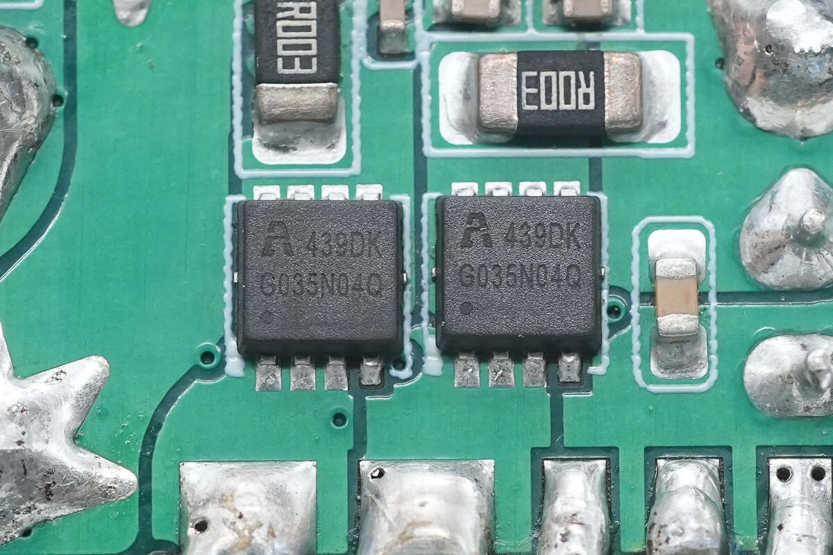
The VBUS MOSFETs for both USB-C ports are from Allpower, model APG035N04Q. They are NMOS devices rated at 40V with an on-resistance of 3.5mΩ, housed in a PDFN 3×3 package.
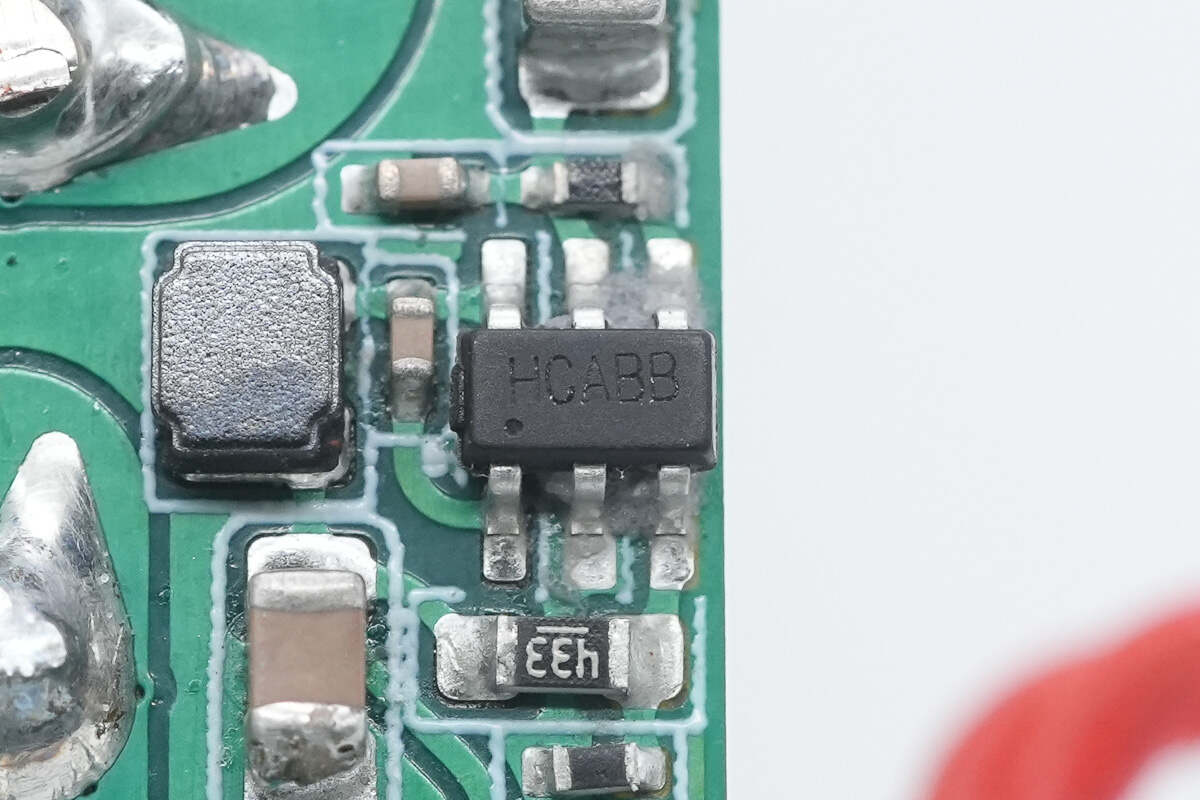
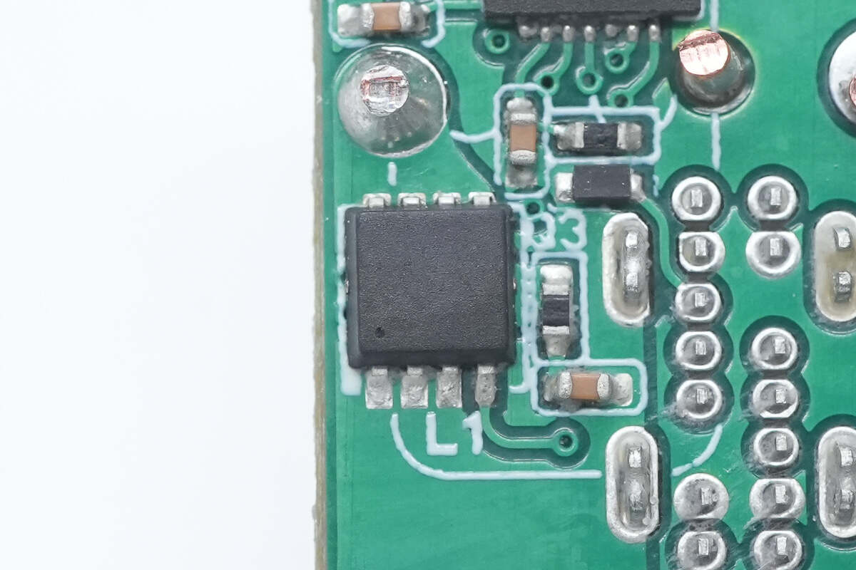
The synchronous buck converter that powers the digital display is marked with HCABB and comes in an SOT23-6 package.
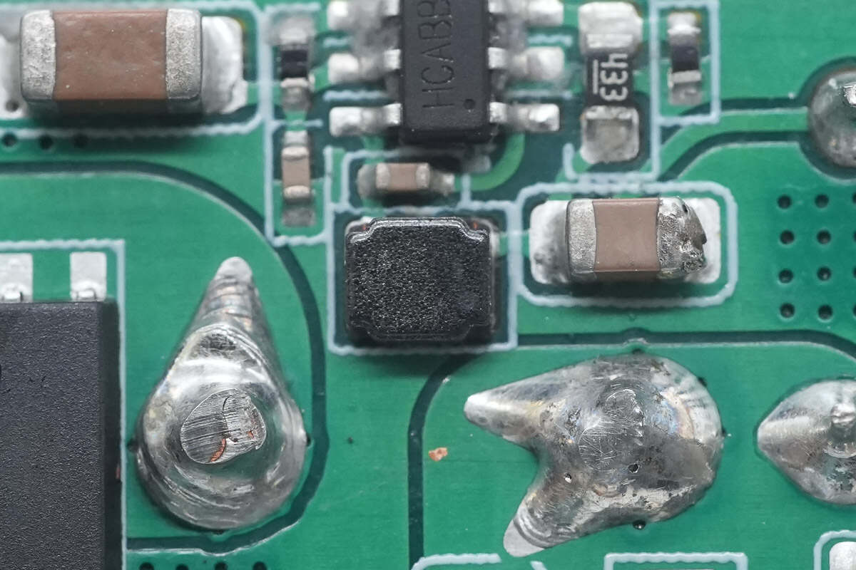
Close-up of the buck inductor.
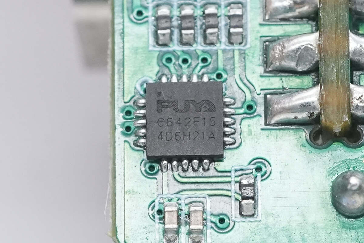
The MCU marked with C642F15 comes in a QFN20 package.
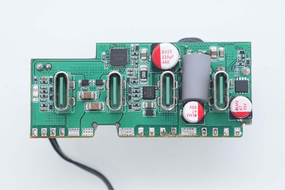
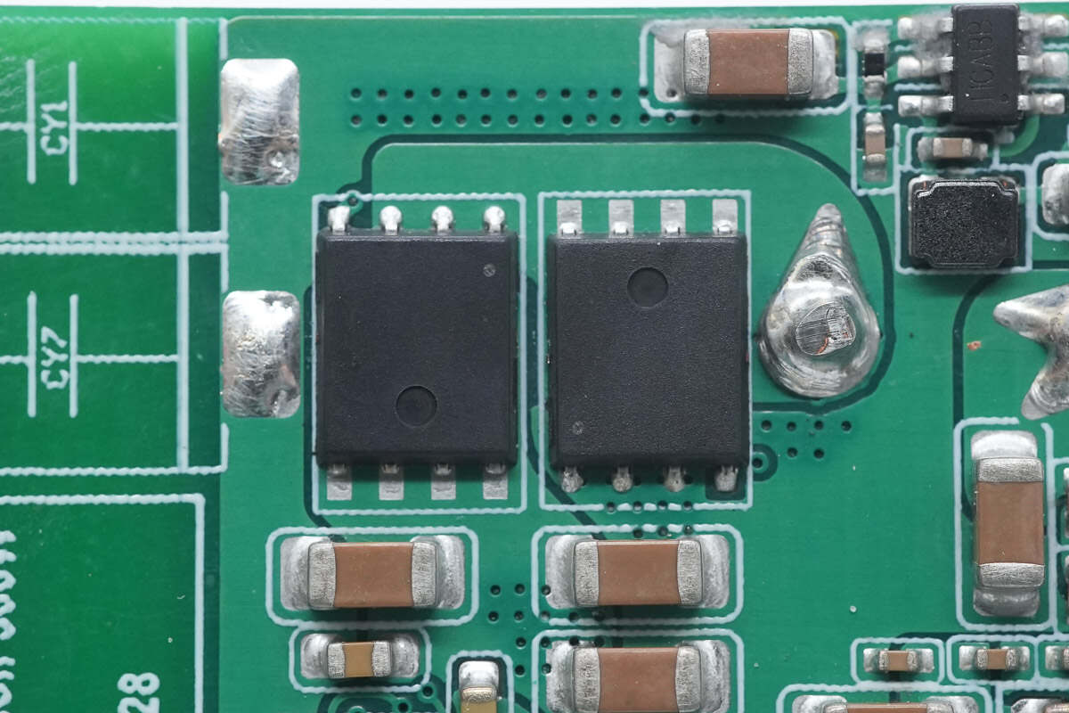
The front side of the PCB holding the four USB-C sockets features buck protocol chips, synchronous buck MOSFETs, a VBUS MOSFET, four solid capacitors, and an LED indicator.
On the back side, there are buck inductors and a thermistor.
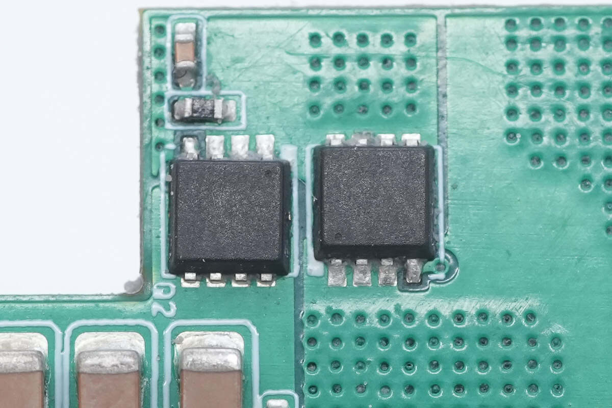
After removing the inductors, a buck protocol chip and a synchronous buck MOSFET are revealed underneath.
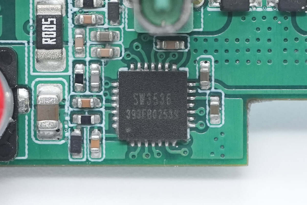
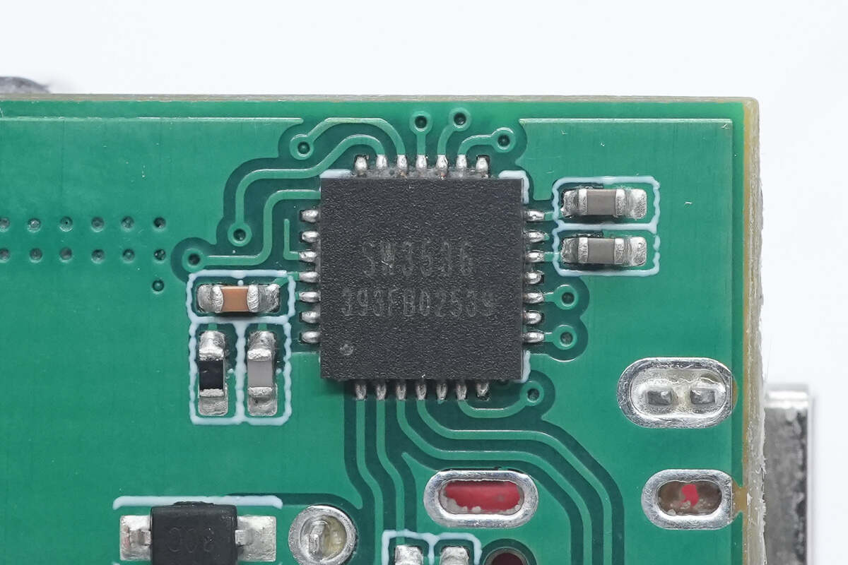
The buck protocol chip for the USB-C3 port is from iSmartWare, model SW3536. It is a highly integrated dual-port fast charging chip supporting USB-A and USB-C dual-port outputs with independent current limiting. It features an internal 7A high-efficiency synchronous buck converter and supports multiple fast charging protocols, including PPS, PD, QC, AFC, FCP, SCP, PE, SFCP, and TFCP. The chip supports a maximum output power of 140W.
The SW3536 integrates CC/CV control, dual-port management logic, and dual-chip dynamic power distribution, with a simplified external component design. It is a complete, high-performance dual-port fast-charging solution supporting multiple protocols. The SW3536 supports up to 36V input voltage, making it suitable for 12–24V input car charger applications, as well as fast-charging adapters, power strips, and car chargers.
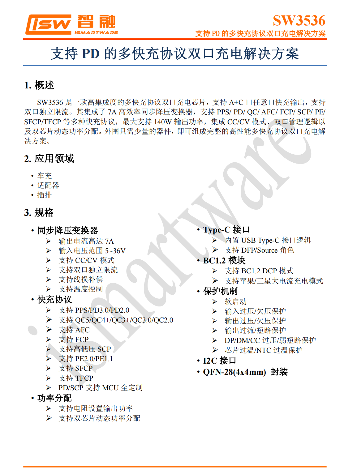
The two synchronous buck MOSFETs paired with it are also unmarked, so their specifications are unknown.
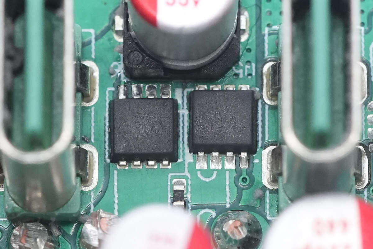
The USB-C4 port also uses the iSmartWare SW3536 as its buck protocol chip.
Close-up of the synchronous buck MOSFET paired with the USB-C4 port.

The other synchronous buck MOSFET is on the front side and is unmarked, so its details are unknown.
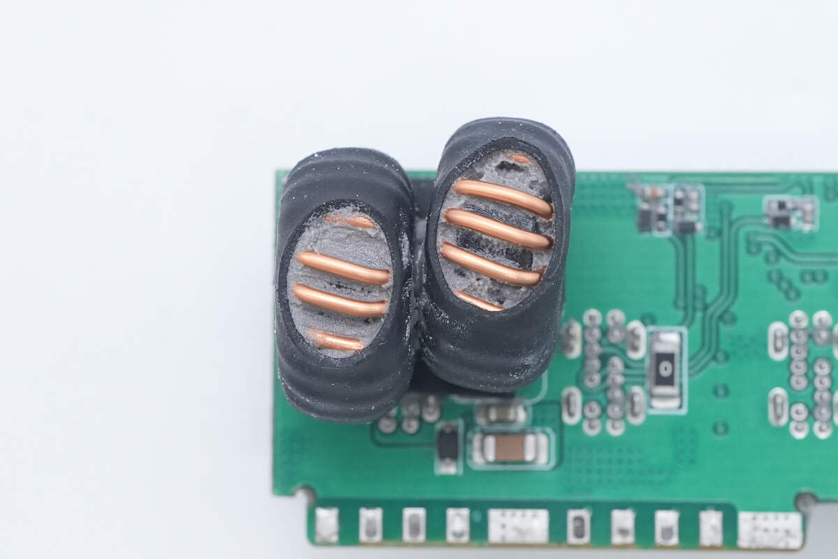
The buck inductors are insulated with heat shrink tubing.
The secondary filter solid capacitors are rated at 25V, 220μF.
This solid capacitor has the same specifications.
The third filter solid capacitor is rated at 35V, 47μF.
The fourth solid capacitor has the same specifications as the third one.
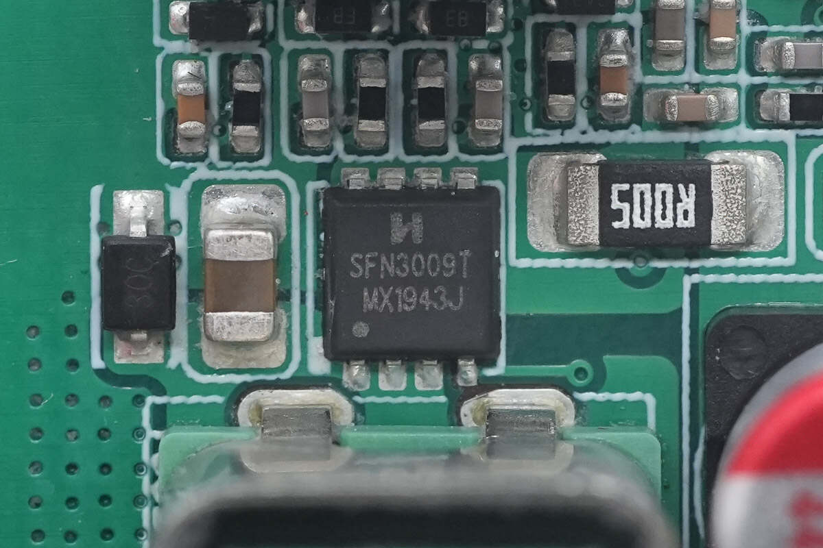
The VBUS MOSFET is from HI-SEMICON, model SFN3009T. It is a 30V NMOS with an on-resistance of 3.5mΩ, packaged in a PDFN 3×3-8L case.
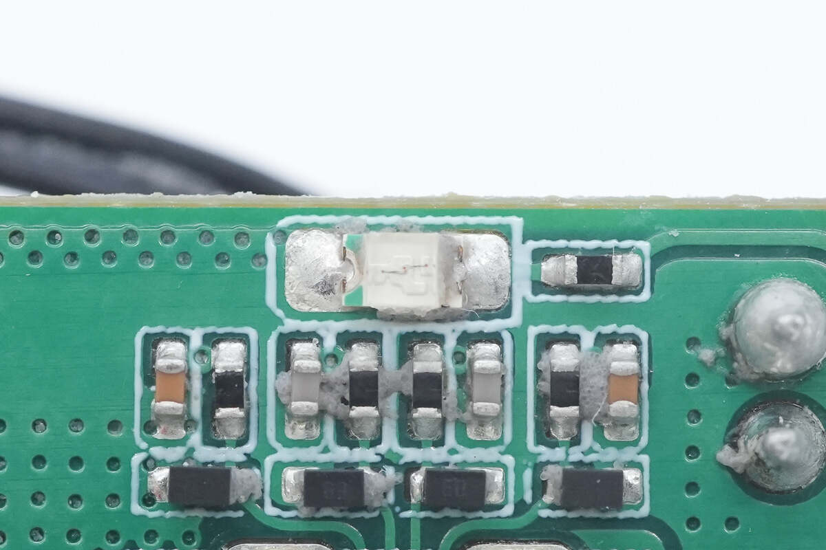
Close-up of the LED indicator.
Close-up of the thermistor.
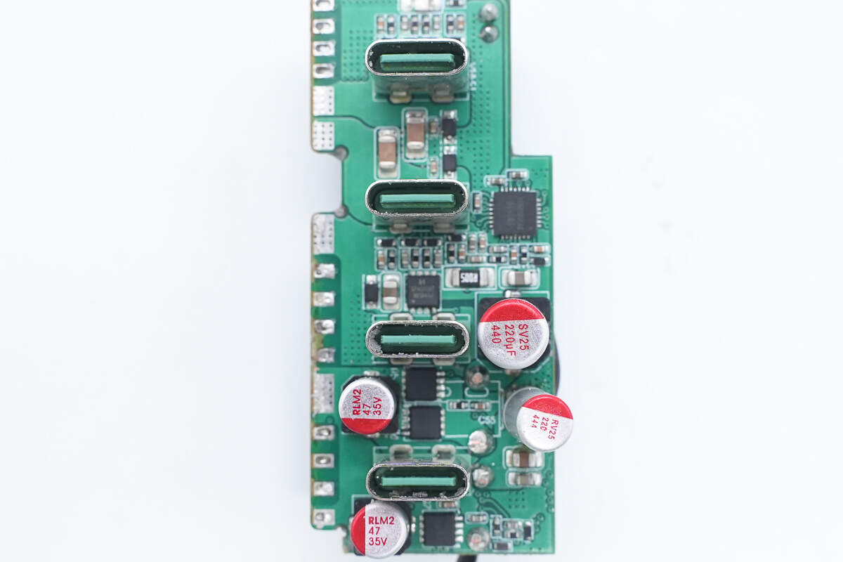
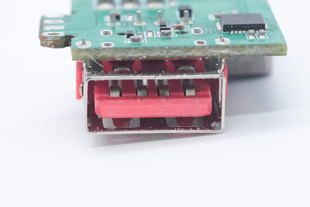
Close-up of the four USB-C sockets.
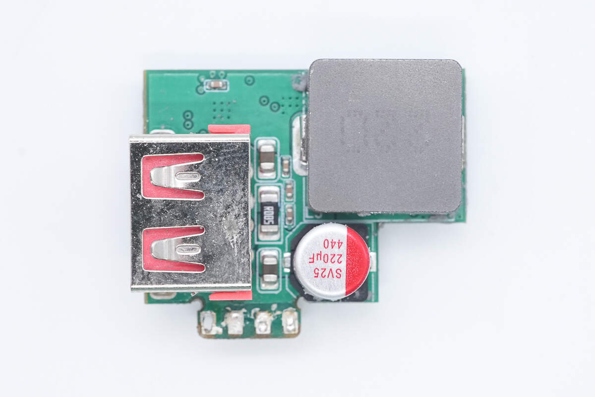
The front side of the PCB with the USB-A socket features a buck inductor and a solid capacitor.
The other side houses the buck protocol chip and two synchronous buck MOSFETs.
The USB-A port also uses the iSmartWare SW3536 as its buck protocol chip.
The two synchronous buck MOSFETs are unmarked, so their details are unknown.
Close-up of the 22μH alloy buck inductor.
The buck output filter solid capacitor is rated at 25V, 220μF.
Close-up of the USB-A socket.
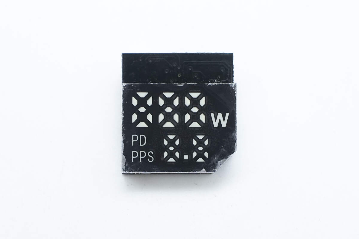
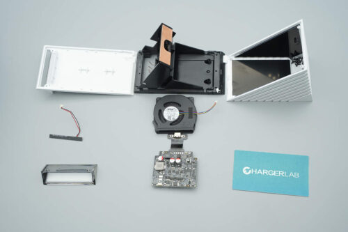
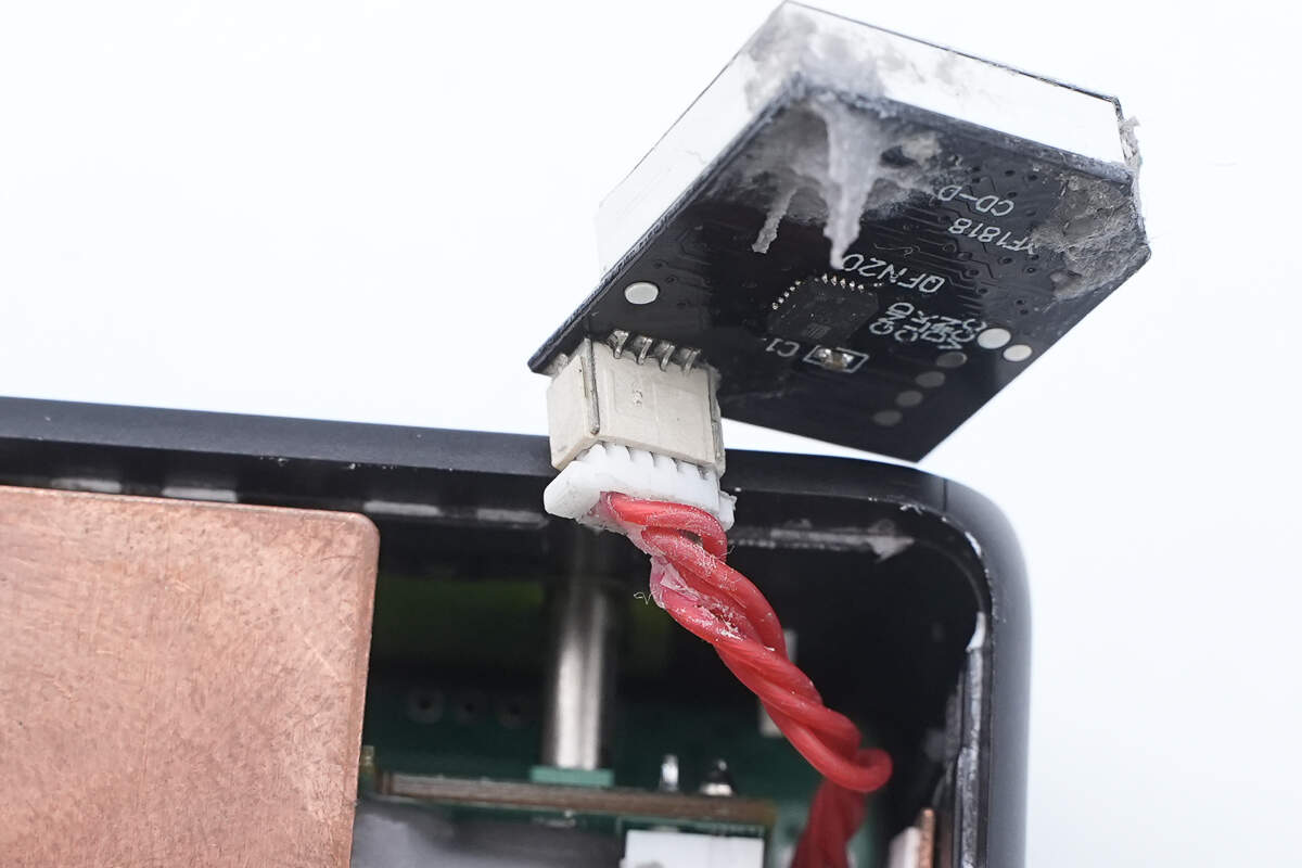
Close-up of the digital display screen.
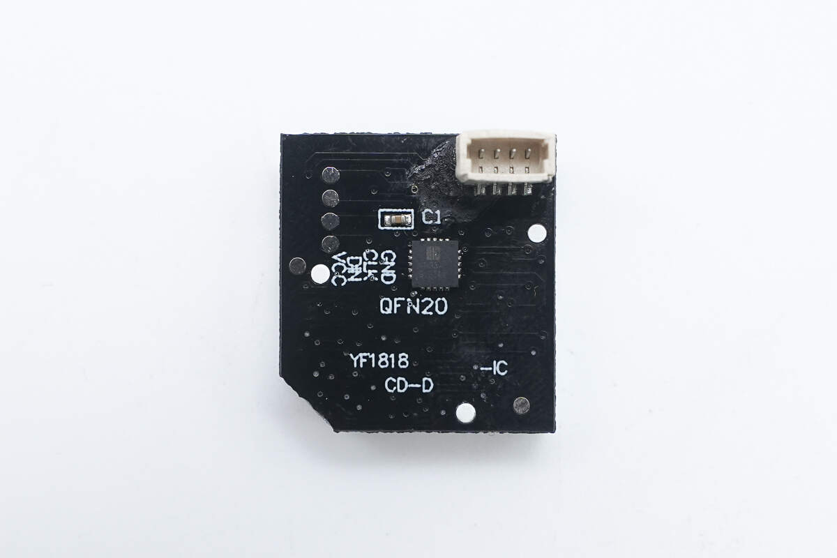
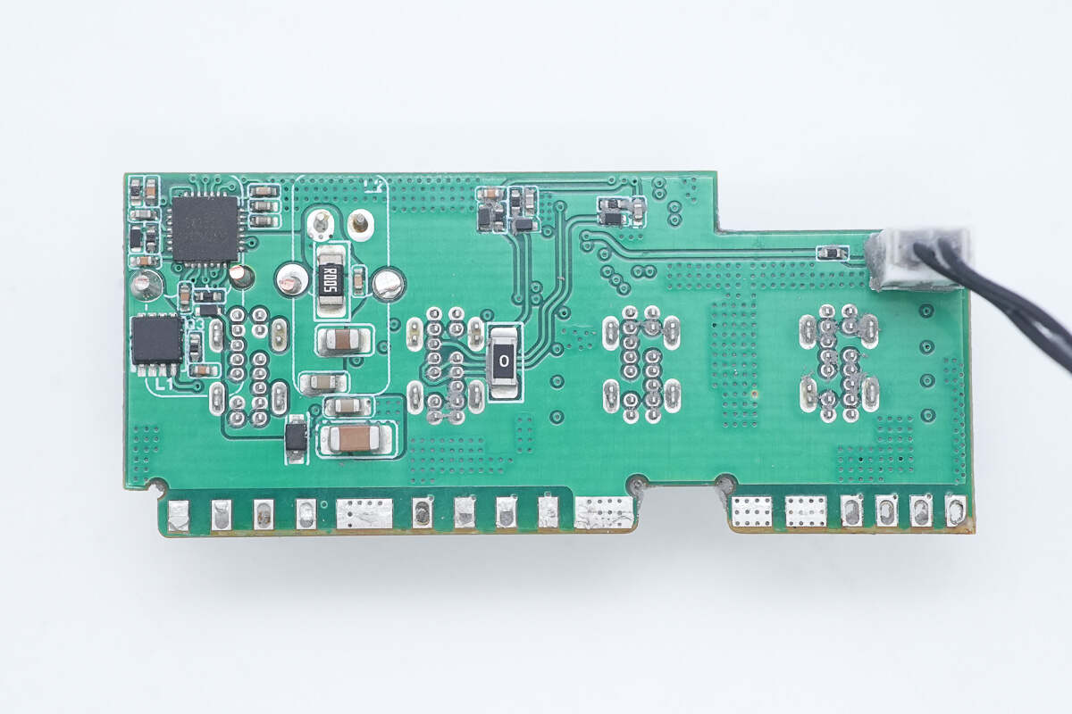
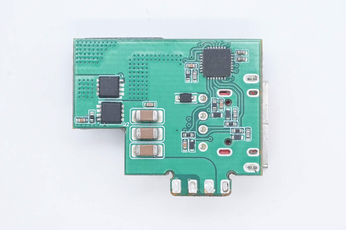
On the back side, there is a connector slot and an LED digital display driver chip.
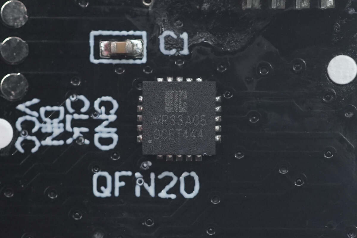
The chip used for driving the LED digital display is from I-CORE, marked with AIP33A05, and comes in a QFN20 package.
Well, those are all components of the HUNDA 300W USB-C GaN Charging Station.
Summary of ChargerLAB
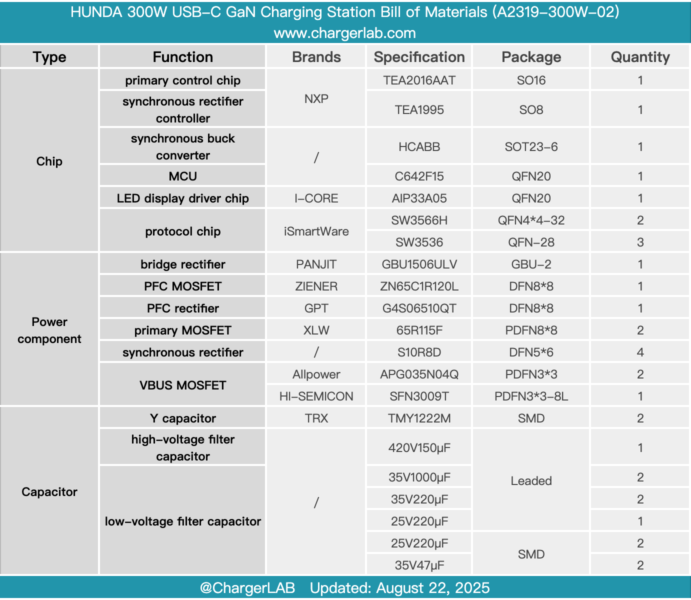
Here is the component list of the HUNDA 300W USB-C GaN Charging Station for your convenience.
The input cable features a detachable design, allowing users to switch power cords to suit different countries and regions. Two of the USB-C ports support 140W output, offering up to 300W of total output power. It supports protocols such as UFCS, SCP, PD, and PPS, providing broad compatibility.
After taking it apart, we found that it is designed based on a high-efficiency PFC+LLC topology, utilizing a fully integrated power solution with the NXP TEA2016AAT and TEA1995. It is paired with high-performance power components such as the ZIENER ZN65C1R120L GaN chip and the GPT G4S06510QT SiC diode.
The five output ports are powered by five independent DC-DC circuits. Secondary buck conversion and output control are handled by two iSmartWare SW3566H chips and three SW3536 buck protocol chips. The front and back of the PCBA module are equipped with thermal gel and a thermal pad, respectively, and an integrated copper heatsink is used to assist in heat dissipation, ensuring stable performance under high-power output conditions.
Related Articles:
1. Teardown of UGREEN Nexode Car Charger 145W with Retractable USB‑C Cable (EC604)
2. Teardown of Lenovo thinkplus 240W Qlex Dual USB-C Retractable Cable (CBQX240A)
3. Teardown of UGREEN 120W DC UPS (US3000)