Introduction
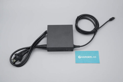
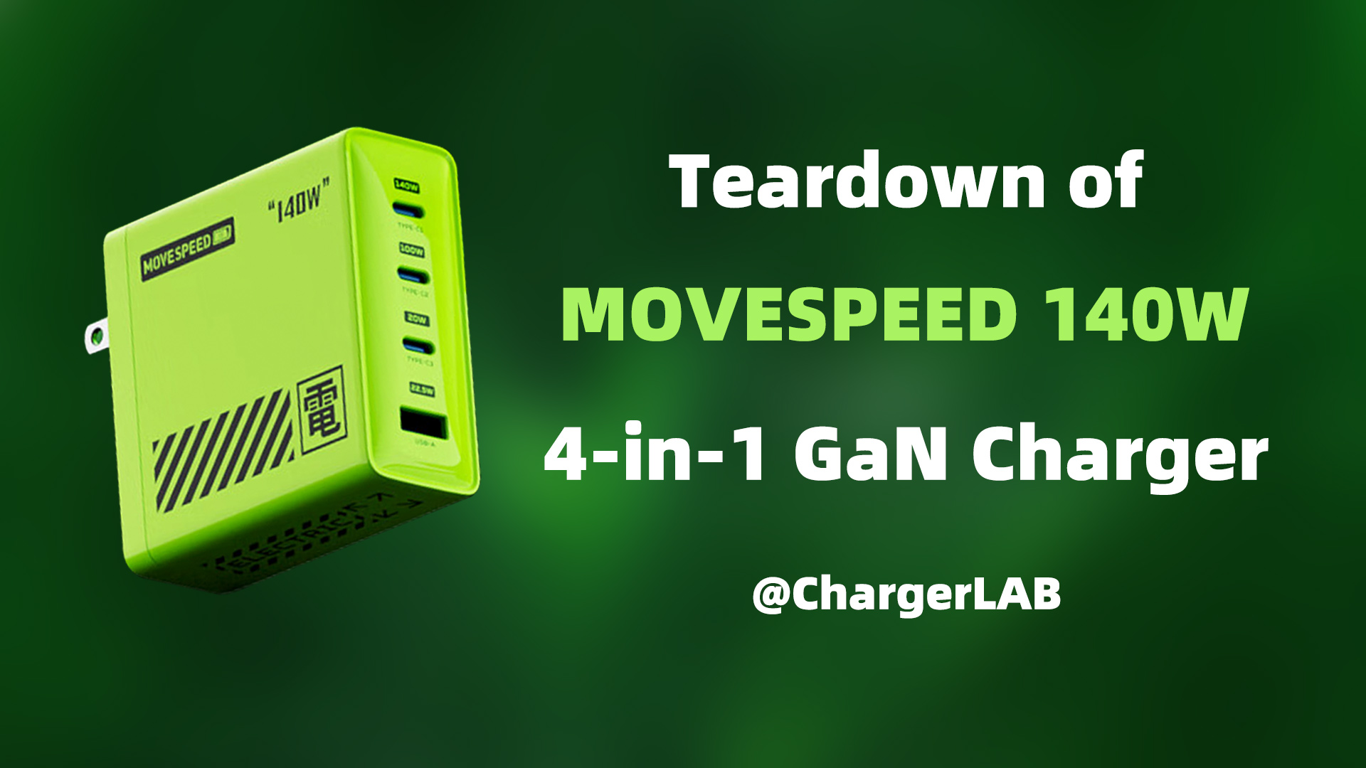
Today, we’re bringing you a teardown of the new EcoFlow RAPID Pro 140W 4-Port GaN Charger. This product is designed based on advanced GaN technology, combining a sleek appearance, multiple ports, high-power fast charging, and a compact, portable form factor.
The charger features three USB-C ports and a USB-A configuration. Among them, two USB-C ports support the USB PD 3.1 fast charging standard, delivering up to 28V/5A 140W output. The remaining USB-C and USB-A ports each support 30W fast charging. It also supports multiple intelligent output configurations, such as 65W + 45W + 30W, providing enhanced performance and better device compatibility. Now, let’s take a closer look at its internal design and structure.
Product Appearance

The front of the packaging features the EcoFlow logo, product name, and an image of the charger.

The back of the packaging displays usage scenarios and detailed specifications of the product.

The package includes the charger, a user manual, and a thank-you card.

The outer shell is made of flame-retardant PC material with a silver-gray metallic paint finish.

The center of the front panel features the EcoFlow logo.

The opposite side is labeled with "140W GaN".

One side of the device is printed with the specification details.

Model: EF-WC-140-CN
Input: 110–240V\~ 50/60Hz 3.2A Max
Output:
Type-C1 / Type-C2: 5V⎓3A, 9V⎓3A, 12V⎓3A, 15V⎓3A, 20V⎓5A, 28V⎓5A (140W Max)
Type-C3 / USB-A: 5V⎓3A, 9V⎓3A, 12V⎓2.5A (30W Max)
Combined Output Configurations:
Type-C1 + Type-C2: 70W + 70W
Type-C3 + USB-A: 18W
Type-C1/C2 + Type-C3/USB-A: 100W + 30W
Type-C1/C2 + (Type-C3 + USB-A): 100W + 18W
Type-C1 + Type-C2 + Type-C3: 65W + 45W + 30W
Type-C1 + Type-C2 + USB-A: 65W + 45W + 18W
Type-C1 + Type-C2 + (Type-C3 + USB-A): 65W + 45W + 18W
Total Output Power: 140W

It has passed the CCC certification.

It has foldable pins.

On the output side, there are four USB ports, each labeled with its corresponding output power next to the port.

The length of the charger is about 63.18 mm (2.49 inches).

The width is about 66.99 mm (2.64 inches).

The thickness is about 30.78 mm (1.21 inches).

Its size is much smaller than the Apple 140W charger.

That's how big it is in the hand.

The weight is about 224 g (7.9 oz).

ChargerLAB POWER-Z KM003C shows that the USB-C1 supports UFCS, QC3+/5, FCP, SCP, AFC, PD3.1, PPS, DCP, SAM 2A, and Apple 2.4A charging protocols.

And it has six fixed PDOs of 5V3A, 9V3A, 12V3A, 15V3A, 20V5A, and 28V5A. It has one set of PPS, which is 5-21V5A. Additionally, it includes a 15–28V 140W AVS voltage profile.

Testing shows that the USB-C2 port supports the same protocols as the USB-C1 port.

The PDO messages are also identical.

The USB-C3 supports QC3+/4+, FCP, SCP, AFC, SFCP, PD3.0, PPS, DCP, SAM 2A, and Apple 2.4A charging protocols.

And it has three fixed PDOs of 5V3A, 9V3A, and 12V2.5A. It has one set of PPS, which is 5-11V3A.

The USB-A supports QC3+, FCP, SCP, AFC, SFCP, DCP, SAM 2A, and Apple 2.4A charging protocols.
Teardown
Next, let's take it apart to see its internal components and structure.

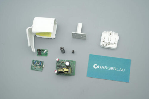
Remove the outer shell. The pins are fixed with a plastic plate and screws and connected to the PCBA module via wires.

Remove the PCBA module.

The length of the PCBA module is about 57.31 mm (2.26 inches).

The width is about 61.19 mm (2.41 inches).

The thickness is about 26.04 mm (1.025 inches).

The PCBA module is encapsulated with potting compound to enhance overall durability and heat dissipation. The top is covered with a Mylar sheet and a heat sink, followed by a layer of blue thermal gel to further improve thermal performance.

The back of the module is also fully covered with potting compound.

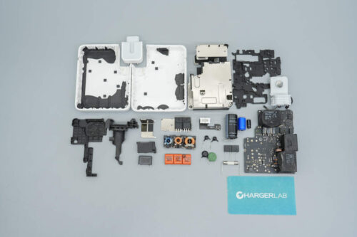
Clean the potting compound. On the front side, there are high-voltage electrolytic capacitors, a filter inductor, a transformer, and other components. Small PCBs are soldered on both sides as well as at the output end.

On the back side, there is a master control chip, a synchronous rectifier controller, synchronous rectifiers, an optocoupler, and other components.

The front end of the PCBA module is equipped with a time-delay fuse, a common mode choke, high-voltage electrolytic capacitors, and film capacitors.

On the other side, there is a small rectifier PCB and a blue Y-capacitor. On the back of the small PCB, there is a bridge rectifier.

Remove the small PCB. The front side is equipped with a safety X capacitor and another bridge rectifier.

The input fuse is from Betterfuse, part number 932, rated at 3.15A 250V.

The NTC thermistor is used to suppress inrush current during power-up.

The thermal protector is from HKW, model HKW9700. Its design here takes advantage of the device’s characteristics: when the power supply is cold, the NTC thermistor effectively suppresses the inrush current at startup. Once the power supply is operating normally, the temperature switch monitors the heat generated by the NTC thermistor and closes the circuit to short it out, thereby optimizing the series loss caused by the NTC thermistor.
This design is quite clever, making full use of the combined properties of the components. It not only suppresses inrush current during cold starts but also improves the power supply’s conversion efficiency and reduces temperature rise.

The common mode choke is used to filter out EMI interference. It is wound with two wires and insulated with a heat-shrink tube for protection.

The safety X capacitor is from JURCC, with a capacitance of 0.22μF.

The bridge rectifier is from NH, model RSBL8010. It is a fast recovery rectifier rated at 8A 1000V and uses an SBL package.

The bridge rectifier on the back side is the same model.

The green high-voltage electrolytic capacitor is from BERYL, rated at 400V 22μF.

The filter inductor is insulated and protected with a heat-shrink tube.

The black electrolytic capacitor is also from BERYL, rated at 250V 100μF.

The other two electrolytic capacitors are from Yuguang, both rated at 250V 82μF.

The red film capacitor is rated at 2.2μF 450V.

On this side, there is a transformer, an SMD Y capacitor, and a second small PCB. The small PCB features a GaN power device with a large exposed copper area coated with solder to enhance heat dissipation.

Remove the small PCB. On the opposite side, multiple small iron blocks are installed to assist with heat dissipation.

The master control chip used is the Chipown PN8215, which integrates a current mode controller and a high-voltage startup module, specifically designed for high-performance fast charging switched-mode power supplies. It features built-in input voltage measurement and X capacitor discharge functions. By monitoring input voltage, output voltage, and load variations, it adaptively switches between PWM, forced DCM, PFM, and Burst Mode operation. This multi-mode modulation technology, combined with specialized low-power device structures, achieves ultra-low standby power consumption and optimal efficiency across the entire input voltage range. Frequency modulation and Soft-Driver technologies ensure excellent EMI performance of the system.
Additionally, it provides comprehensive and high-performance intelligent protection features, including input undervoltage/overvoltage protection, output undervoltage/overvoltage protection, over-temperature protection, secondary rectifier short circuit protection, cycle-by-cycle overcurrent protection, and overload protection. The chip also incorporates built-in high and low voltage detection circuits that control external MOSFETs. When operating at a low input voltage of 110V, it connects a low-voltage capacitor into the circuit, allowing the combination of a smaller high-voltage filter capacitor with a larger low-voltage capacitor, effectively reducing the charger’s size.

The MOSFET used for low-voltage capacitor switching is from PDISEMI, model PDI65R160JF3.

The GaN power chip is from Navitas, model NV6138A. This is a highly integrated GaN power device that incorporates an internal driver and a high-precision lossless current-sensing circuit, eliminating the need for an external current-sense resistor and thereby removing associated power loss. The NV6138A features an internal 120mΩ on-resistance, a 700V-rated GaN FET, and supports switching frequencies up to 2MHz. It comes in a 6×8mm QFN package, providing a larger thermal dissipation area to reduce temperature rise.

Close-up of the transformer.

The blue Y capacitor is from DGCX.

The Everlight EL1019 optocoupler is used for output voltage feedback.

A small PCB is also soldered on the output side.

Remove the small PCB. The PCB is equipped with output VBUS MOSFETs, and on both ends, two sets of secondary buck converter inductors and filter capacitors are also soldered.

Remove the inductor on the left side. Below it, there is also a VBUS MOSFET for the USB-C1 port.

On the back side of the PCB, there are three secondary buck converter protocol chips, synchronous buck MOSFETs, a buck inductor, and a solid capacitor.

After removing the inductor, a set of synchronous buck MOSFETs is located underneath.

The synchronous rectifier controller is from Meraki, model MK91816, designed for flyback topology applications and compatible with CCM, DCM, and QR operating modes. It utilizes proprietary self-powered technology to supply VCC, allowing direct placement on the positive rail without the need for an auxiliary winding.
A 10ns turn-off delay and a pull-down current of up to 4A help ensure reliable operation in CCM mode. Its proprietary turn-on and turn-off mechanisms maximize the conduction time of the externally driven MOSFETs to achieve the highest possible efficiency. Additionally, it features automatic detection of DCM ringing to prevent false turn-on events.

The synchronous rectifiers are from WAYON, marked with 080N10L4, model WMB080N10LG4. They are NMOS devices with a voltage rating of 100V and an on-resistance of 7.8mΩ, packaged in a PDFN5060-8L package.

The solid capacitors for output filtering are from Koshin, each rated at 35V 470μF.

The buck protocol chip for the USB-C1 port is the iSmartWare SW3566H. It is a highly integrated dual-port charging SoC that supports multiple fast-charging protocols. It supports both USB-C and USB-A interfaces with independent dual-port current limiting. The chip integrates a high-efficiency synchronous buck converter, supporting 20V/7A and 28V/5A outputs. It is compatible with PD 3.1, QC, SCP, UFCS, and other fast-charging protocols, with customizable protocol support, and can deliver up to 140W of output power.

The SW3566H integrates CC/CV modes, dual-port management logic, and bus voltage detection. When paired with the corresponding buck MOSFETs and VBUS MOSFETs, it enables dual-port buck output. The built-in buck converter operates at a frequency of 180kHz and supports both PWM and PFM modes. Protection thresholds such as output current and line loss compensation can be configured via the I²C interface. The internal ADC supports data sampling of nine channels, including input/output voltage, output current, and chip temperature, and can interface with an external MCU for parameter monitoring.
The SW3566H supports an input voltage of up to 36V and a maximum output current of 7A. It features soft-start, input overvoltage/undervoltage protection, output overvoltage/undervoltage protection, output overcurrent/short circuit protection, DP/DM/CC overvoltage protection, overtemperature protection, external NTC thermistor protection, and power limiting protection. The chip is packaged in a QFN 4×4-32 form factor.

The two synchronous buck MOSFETs are from Ruichips, model RUH4040. They are NMOS devices with a voltage rating of 40V and an on-resistance of 8mΩ, packaged in a PDFN3333 package.

The buck protocol chip for the USB-C2 port also uses the iSmartWare SW3566H.

The two synchronous buck MOSFETs for USB-C2 also use Ruichips RUH4040.

Close-up of two buck inductors.

The solid capacitor is from JSH, rated at 35V 150μF.

The other capacitor is the same model, and both are covered with insulating sleeves.

The output VBUS MOSFET for the USB-C1 port also uses the Ruichips RUH4040.

The output VBUS MOSFET for the USB-C2 port also uses the Ruichips RUH4040.

The buck protocol chip used for the USB-C3 and USB-A ports is the iSmartWare SW3537. It integrates a 5A high-efficiency synchronous buck converter and supports a wide range of charging protocols, including PPS, PD, QC, AFC, FCP, SCP, PE, SFCP, and low-voltage direct charging. It operates in CC/CV modes and requires only a few external components to form a complete, high-performance dual-port fast-charging solution.
Thanks to its high level of integration, the SW3537 combines the protocol chip, synchronous buck controller, and buck MOSFETs into a single package, greatly simplifying the circuit design for multi-port fast charging. The chip supports dual-port fast charging applications (A+C) and comes with comprehensive protection features.

Here is the information about iSmartWare SW3537.

The buck inductor is insulated with a heat-shrink tube.

The buck output filter capacitor is from BERYL, rated at 25V 220μF.

The VBUS MOSFET is from Vergiga, model VS3622DE. It is a dual NMOS device with a voltage rating of 30V and an on-resistance of 10mΩ. It supports 5V logic-level driving and comes in a PDFN3333 package.

Here is the information about Vergiga VS3622DE.

Close-up of the thermistor.

Close-up of three USB-C port sockets.

Well, those are all components of the EcoFlow RAPID Pro 140W 4‑Port GaN Charger.
Summary of ChargerLAB

Here is the component list of the EcoFlow RAPID Pro 140W 4‑Port GaN Charger for your convenience.
It features 3 USB-C ports and 1 USB-A port, supporting 140W and 30W outputs, and supports output configurations such as 100W+30W, 70W+70W, and 65W+45W+30W.
After taking it apart, we found that it uses the Chipown PN8215 solution, enabling a hundred-watt fast-charging design without a PFC circuit. By eliminating the need for a PFC controller and boost inductor, this approach effectively reduces development complexity and costs. Combined with a high- and low-voltage filter capacitor switching function, it efficiently controls the size of hundred-watt fast chargers, enabling product miniaturization and offering a new option for market product designs.
It adopts a flyback architecture design, with the primary GaN FET being the Navitas NV6138A, and the secondary side using the Meraki MK91816 paired with WAYON synchronous rectifiers. Buck outputs are managed by two iSmartWare SW3566H chips and one SW3537 chip. Capacitors from Koshin, BERYL, and JSH are used. The PCBA module is filled with potting compound and covered with a heat sink, ensuring high-quality workmanship and reliable components.
Related Articles:
1. Teardown of MSI 140W USB-C Power Adapter (ADP-140AB B)
2. Teardown of MECHREVO 140W USB-C GaN Power Adapter (AY140AA-1C-CH)
3. Teardown of Meituan 7000mAh 22.5W Shared Power Bank (MT-D-7BDY0)