Introduction
CUKTECH has recently released a new power bank, the No.10 Super Magnetic Power Card. It features a next-generation silicon–carbon battery and incorporates CUKTECH’s self-developed ADC+OPC fast-charging technologies. With a 55 W charging output, it can charge the Xiaomi 17 Pro to approximately 67% in 30 minutes. The device also supports up to 15 W wireless output.
It is equipped with a TFT high-definition display that shows real-time information such as battery level, port status, power input and output, and estimated charging or discharging time. Users can also customize screen brightness and interface orientation. Next, let’s take a closer look at its internal components and design.
Product Appearance
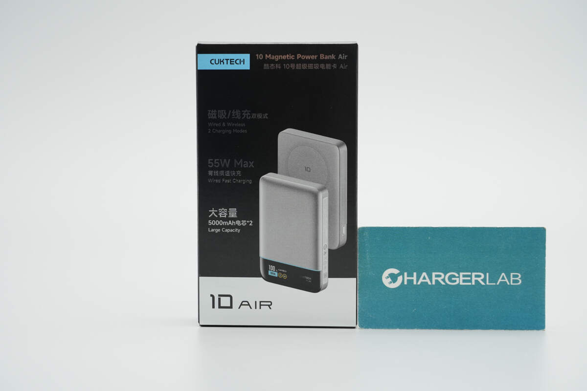
The front of the packaging box displays the CUKTECH logo, the product name, an image of the device, and its key selling points.
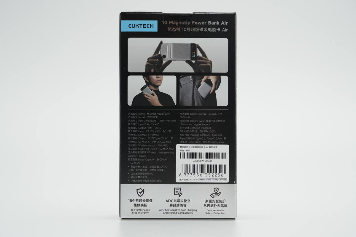
The back of the box lists the specifications, precautions, and selling points.
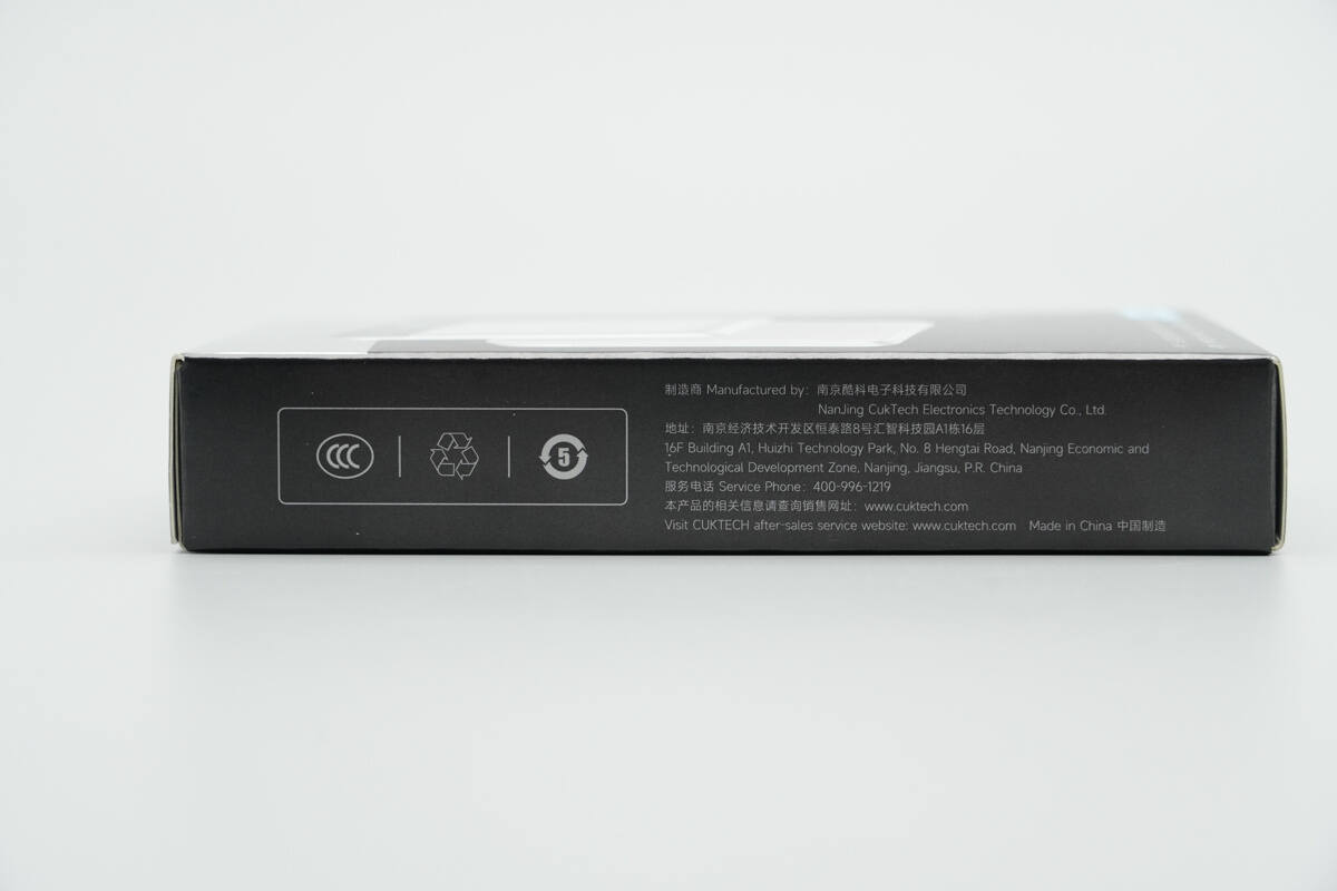
The side of the box includes information about the manufacturer, and the product is certified under the CCC standard.
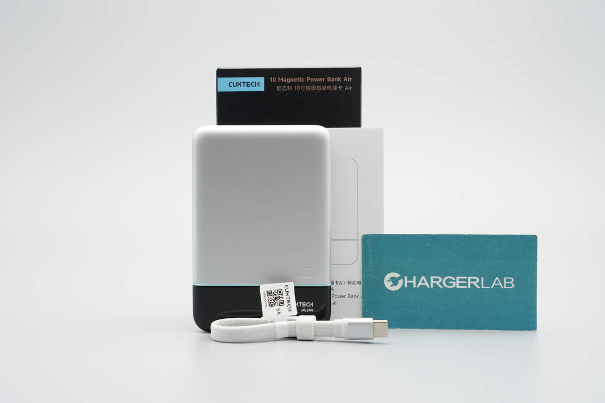
The package includes the CUKTECH 10 Super Magnetic Power Card, a charging cable, and a user manual.
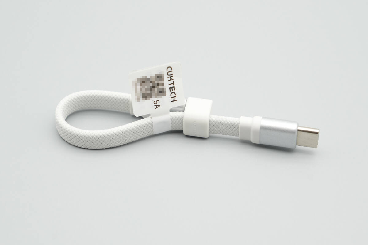
The included braided cable is detachable.
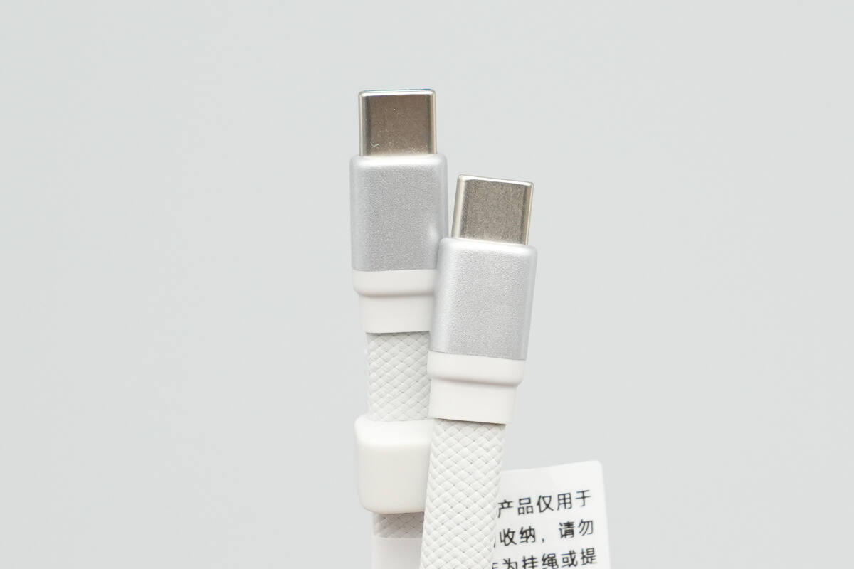
The cable’s connectors use plastic housings with a metallic paint finish.
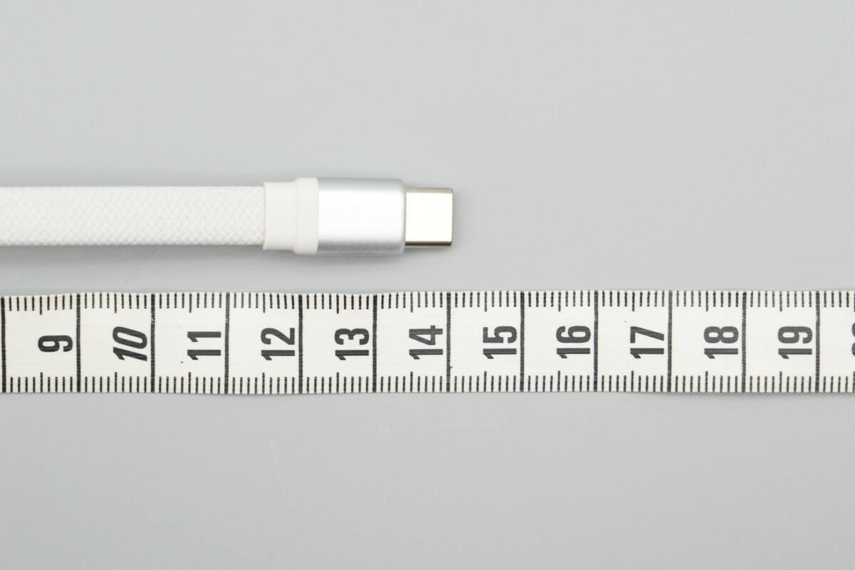
The length of the cable is about 14 cm (5.51 inches).
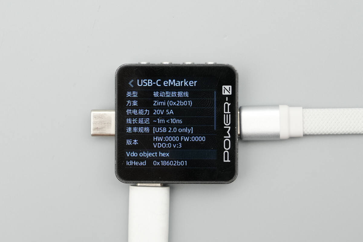
ChargerLAB POWER-Z KM003C shows it has an E-Marker chip, supports power delivery up to 20V5A, and offers data transfer capability compliant with the USB 2.0 standard.
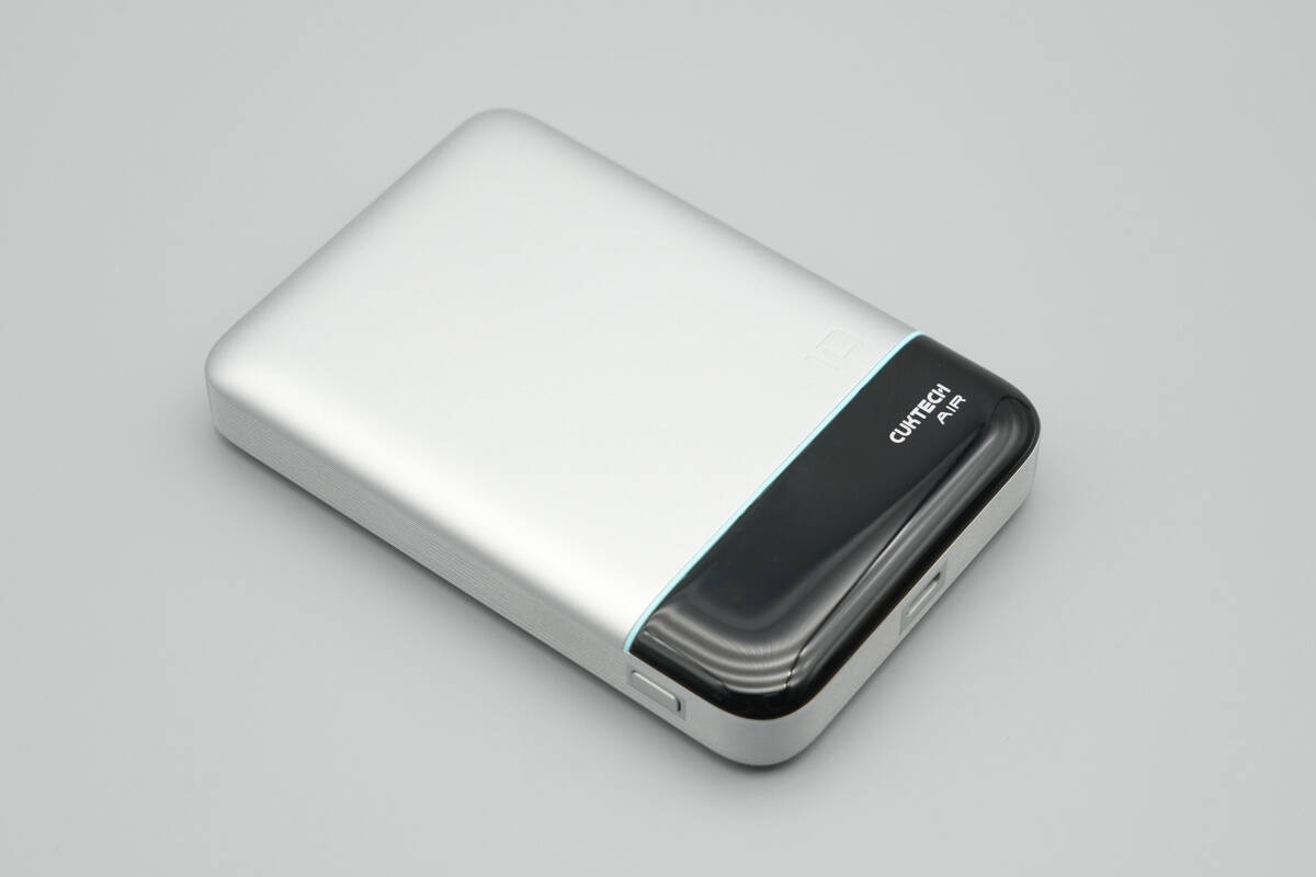
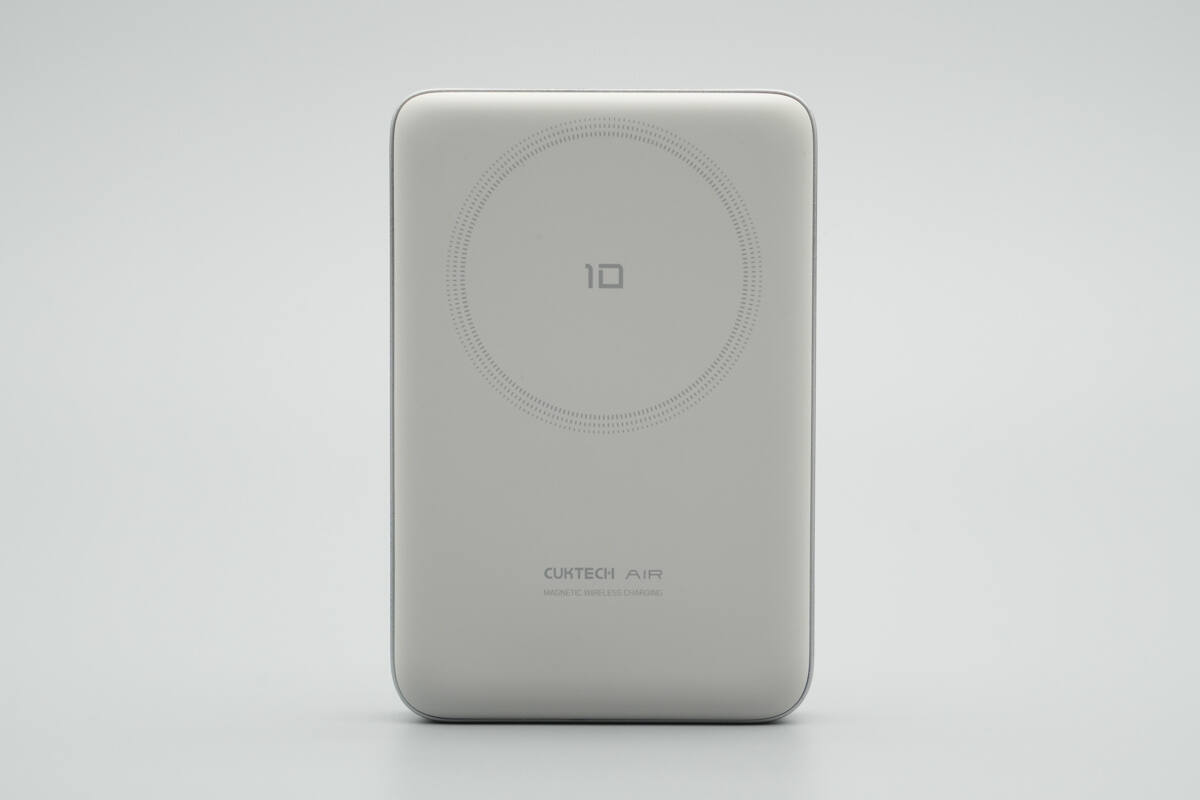
The front features a silver-white paint finish, with the screen positioned at the lower section.
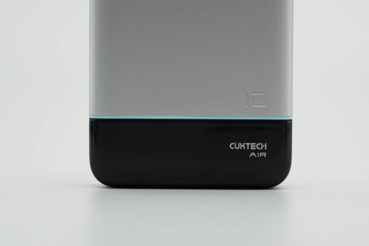
The right side is engraved with “10,” and the black decorative panel is printed with “CUKTECH AIR.”
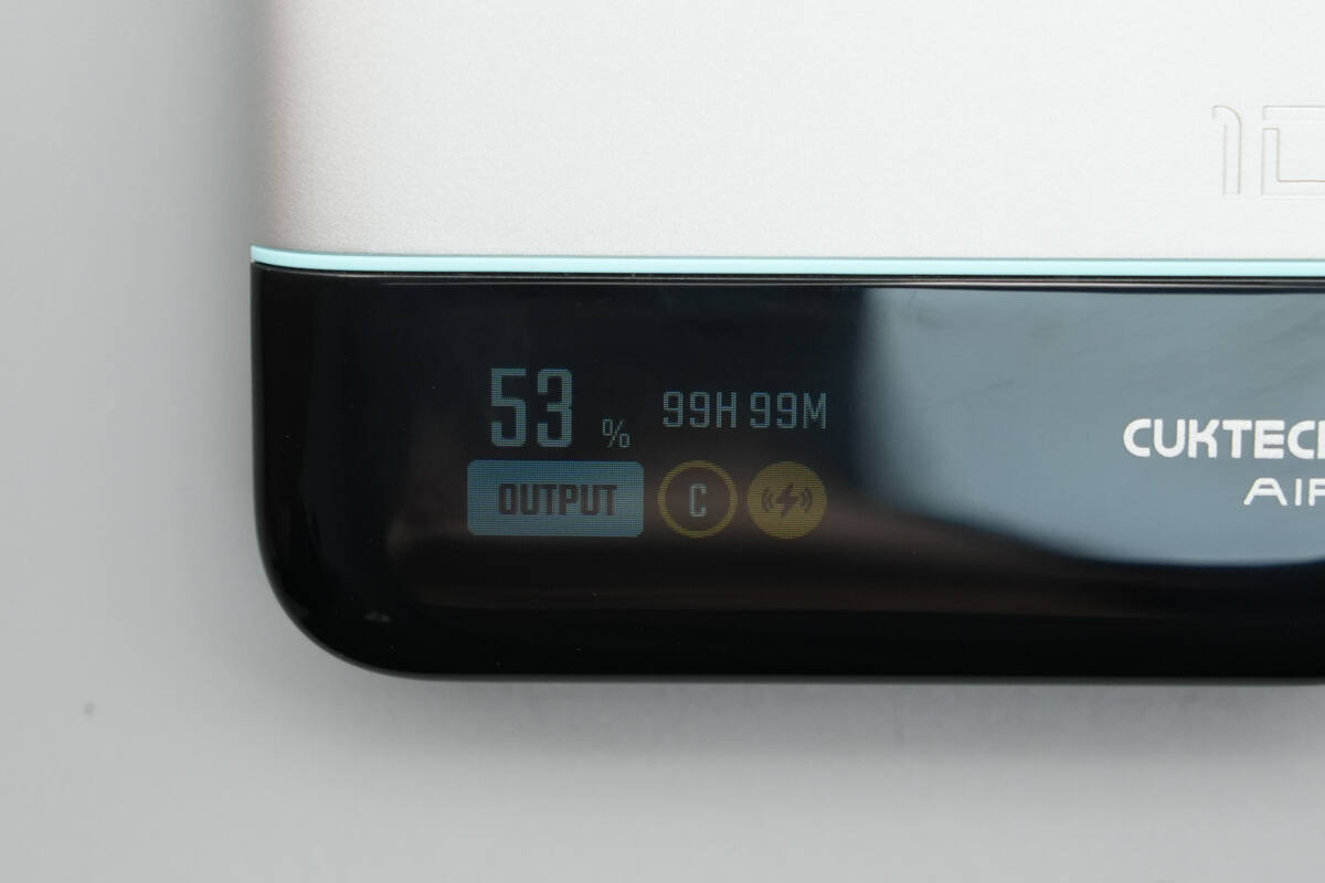
The left side houses a TFT high-definition display that shows real-time information such as battery level, port status, power input and output, and remaining charging or discharging time.
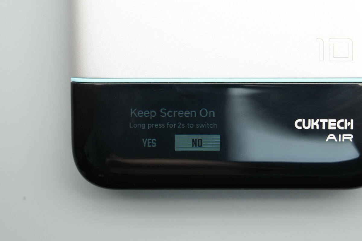
The display can also be set to stay on continuously or turn off automatically after 60 seconds, according to user preference.

The screen orientation can also be adjusted according to user preference.
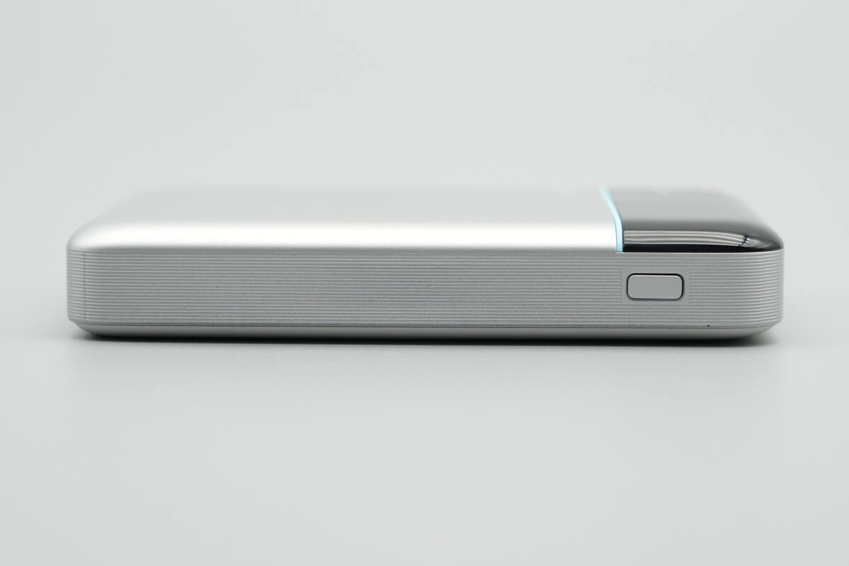
The textured sides enhance grip, and a power button is also provided.
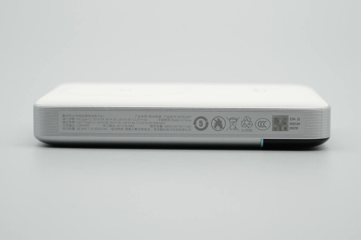
The opposite side displays the specifications.
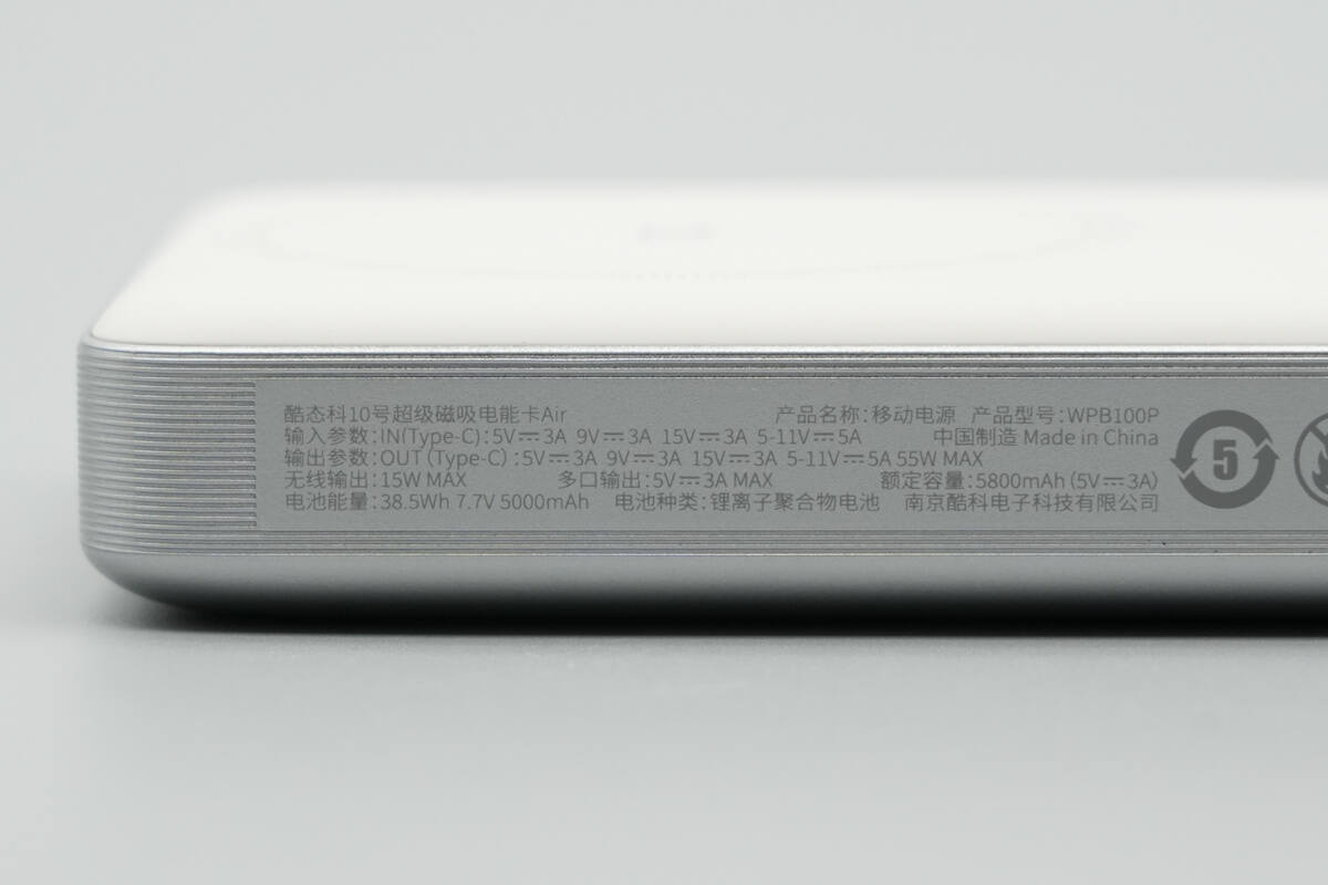
Product Model: WPB100P
Input Specifications:
Type-C: 5V⎓3A, 9V⎓3A, 15V⎓3A, 5–11V⎓5A
Output Specifications:
Type-C: 5V⎓3A, 9V⎓3A, 15V⎓3A, 5–11V⎓5A, 55W MAX
Wireless Output: 15W MAX
Multi-Port Output: 5V⎓3A MAX
Rated Capacity: 5800mAh (5V⎓3A)
Battery Energy: 38.5Wh, 7.7V, 5000mAh
Battery Type: Lithium-ion polymer battery
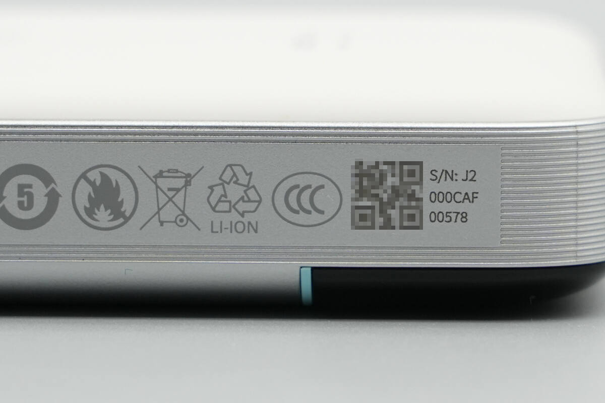
The product is certified under the CCC standard.
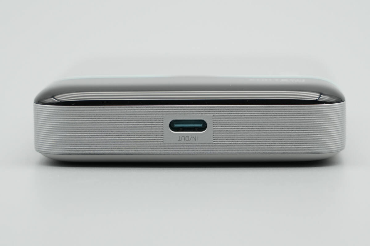
The bottom is equipped with a bidirectional USB-C fast-charging port.
The magnetic surface is made of liquid silicone, which increases friction to securely attach to a phone.
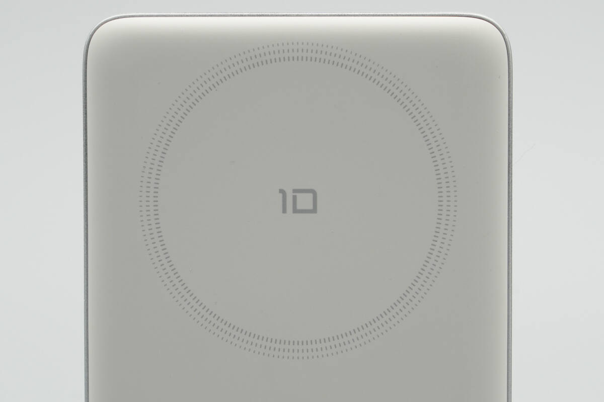
The top features a circular indicator marking the wireless charging area, with a “10” printed in the center.
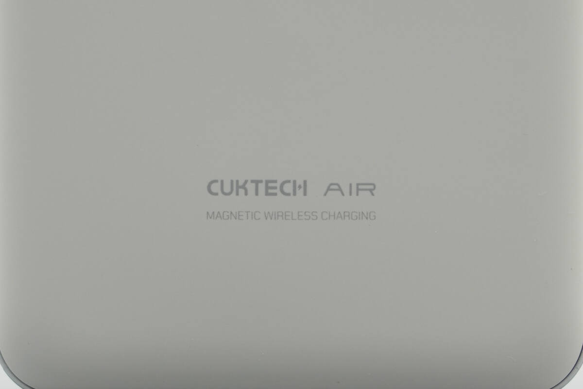
The bottom is printed with “CUKTECH AIR” and “MAGNETIC WIRELESS CHARGING.”
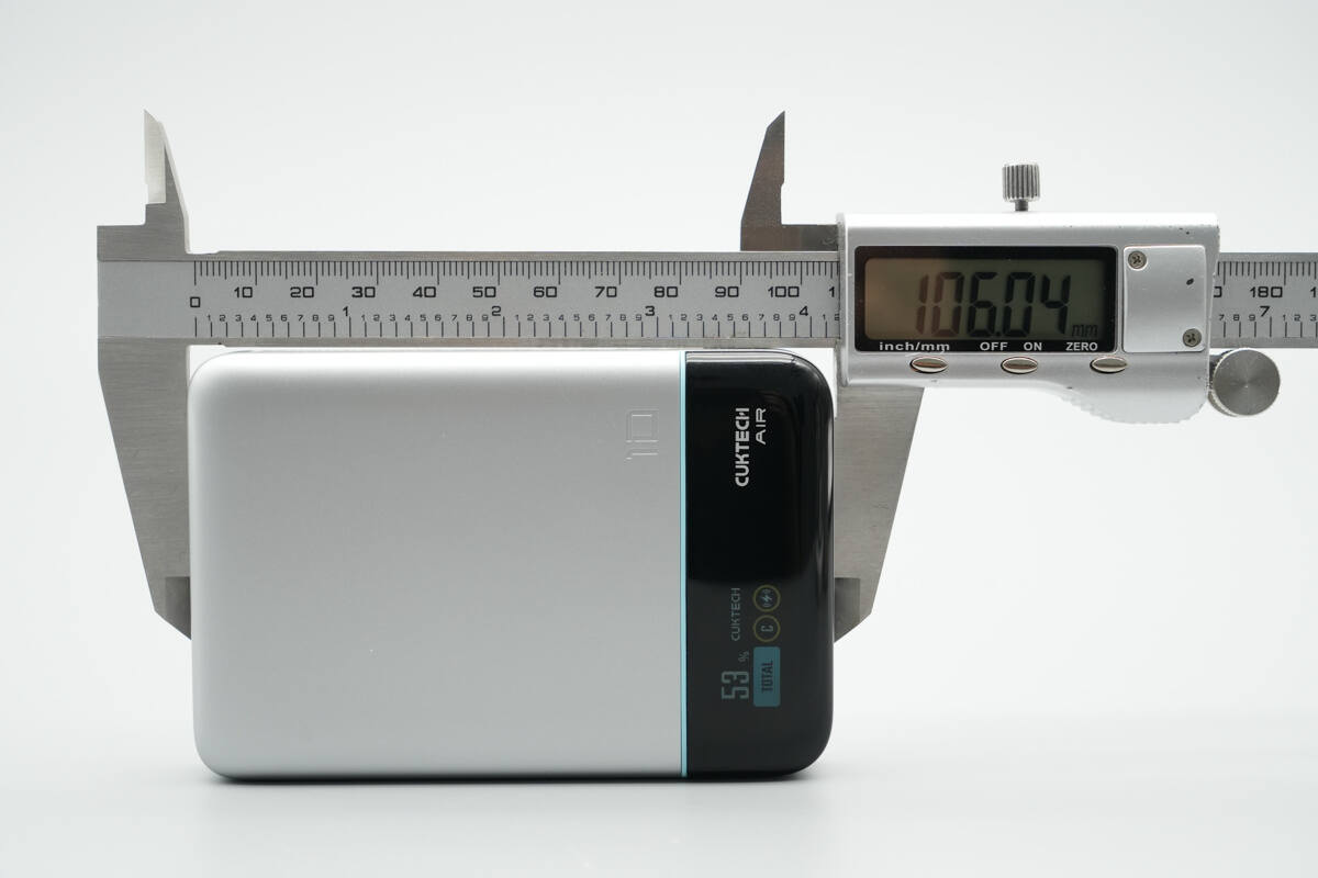
The length of the power bank is about 106.04 mm (4.17 inches).
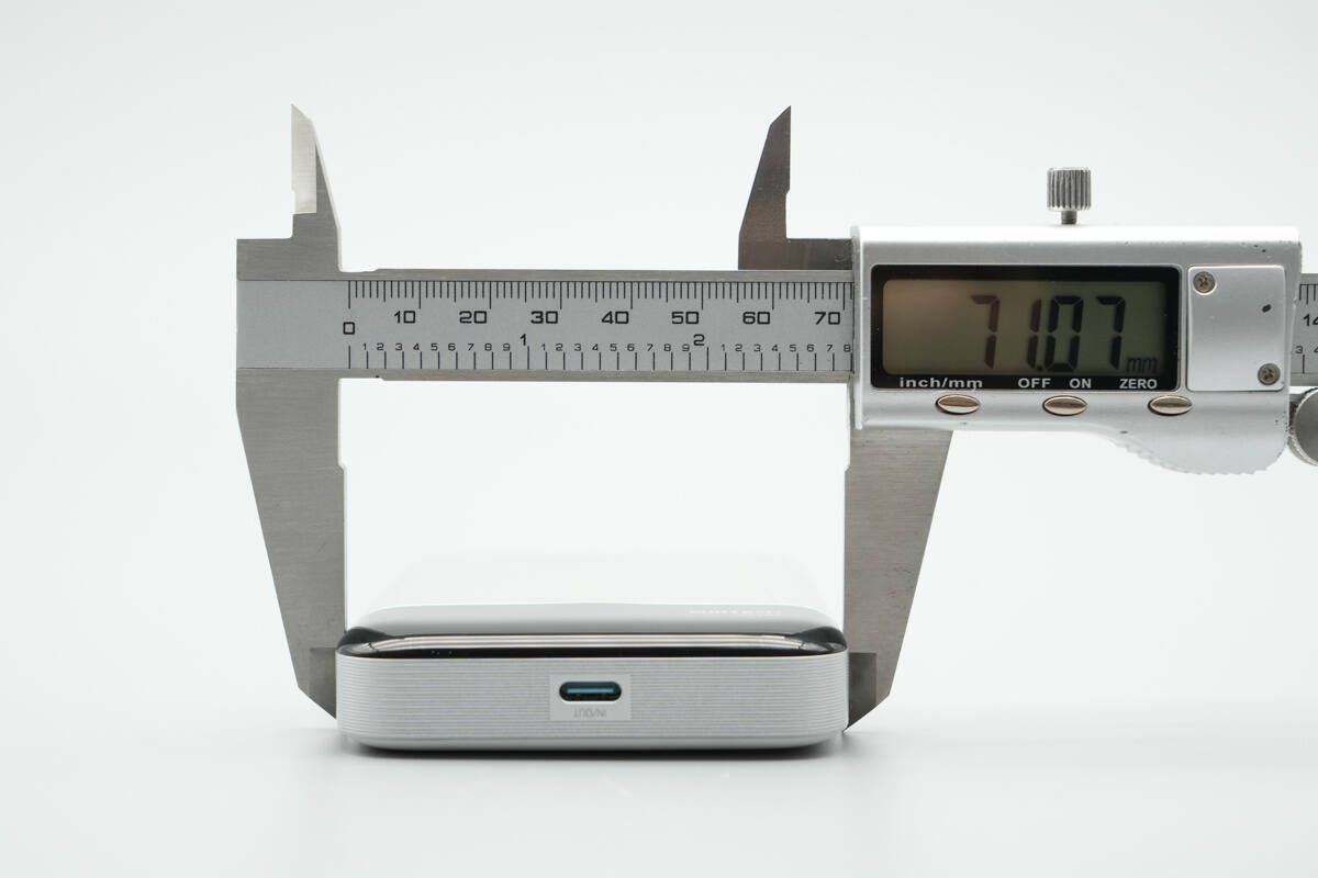
The width is about 71.07 mm (2.8 inches).
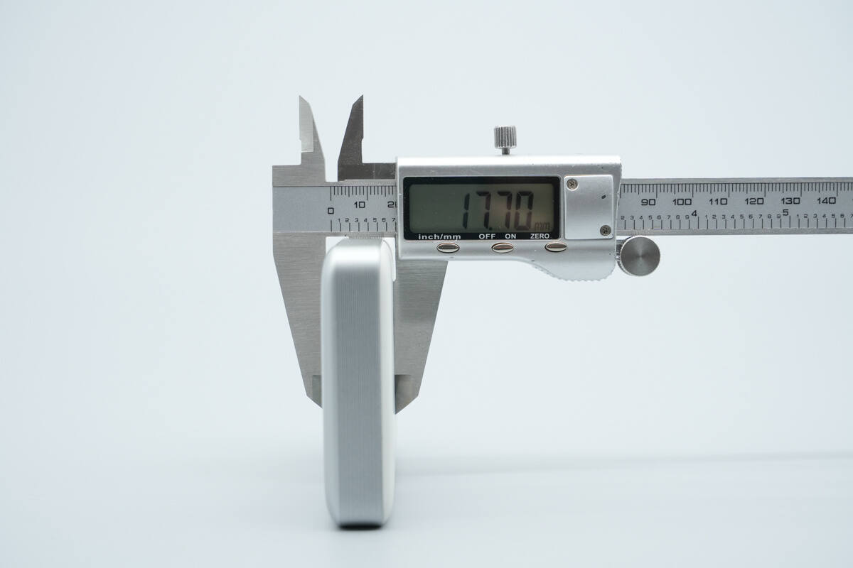
The thickness is about 17.7 mm (0.7 inches).
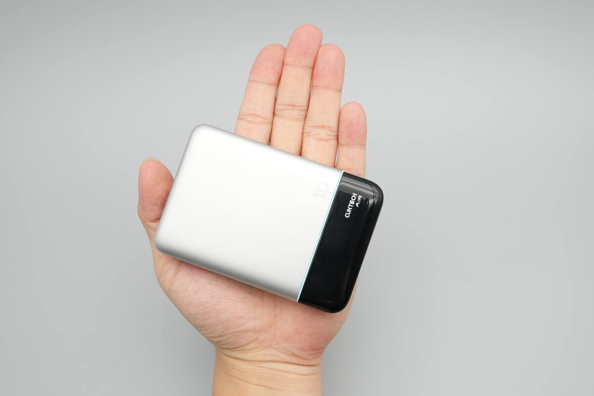
That's how big it is in the hand.
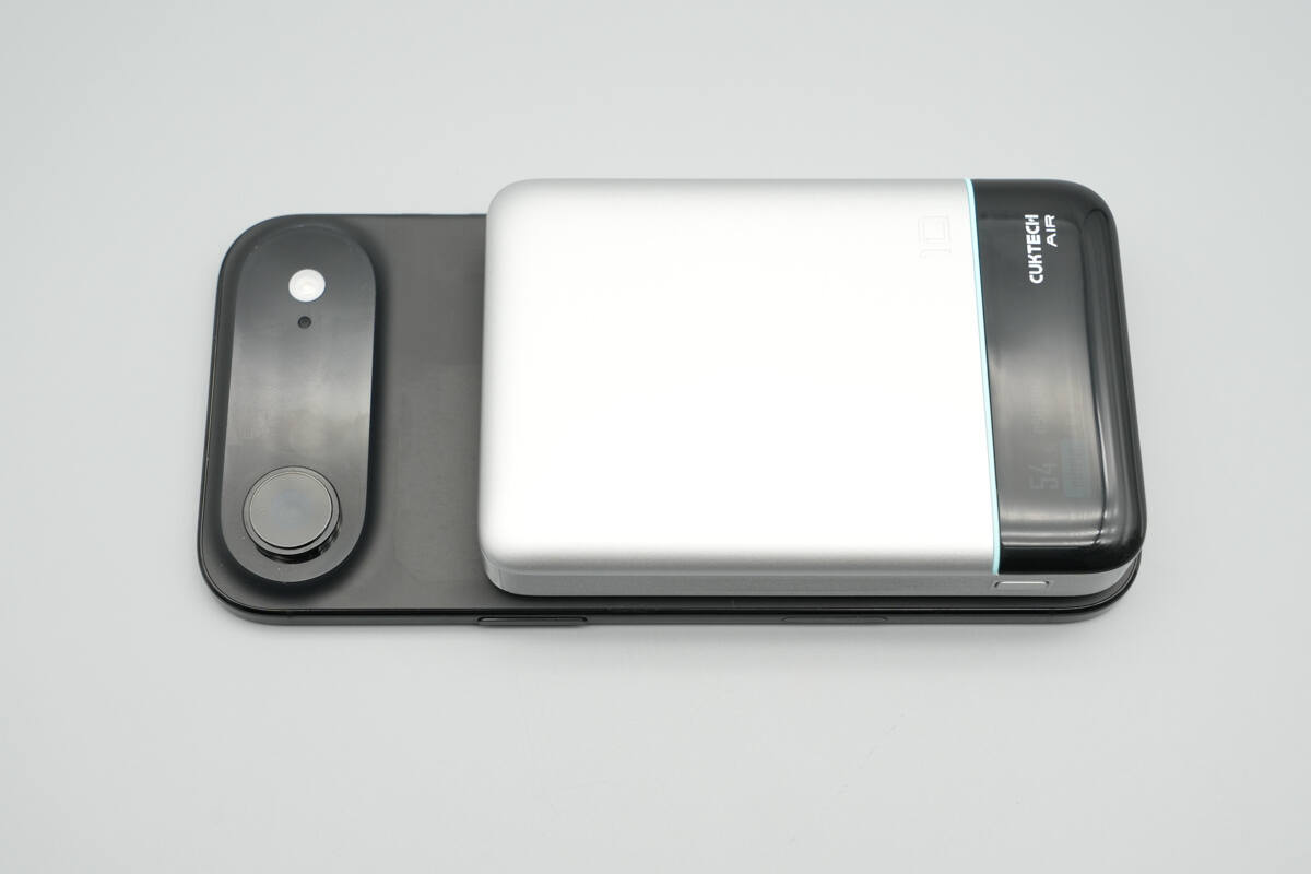
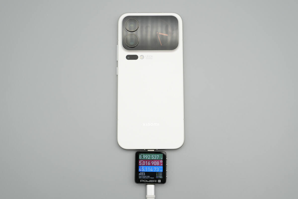
When attached to the back of the iPhone Air, it does not obstruct the rear camera.
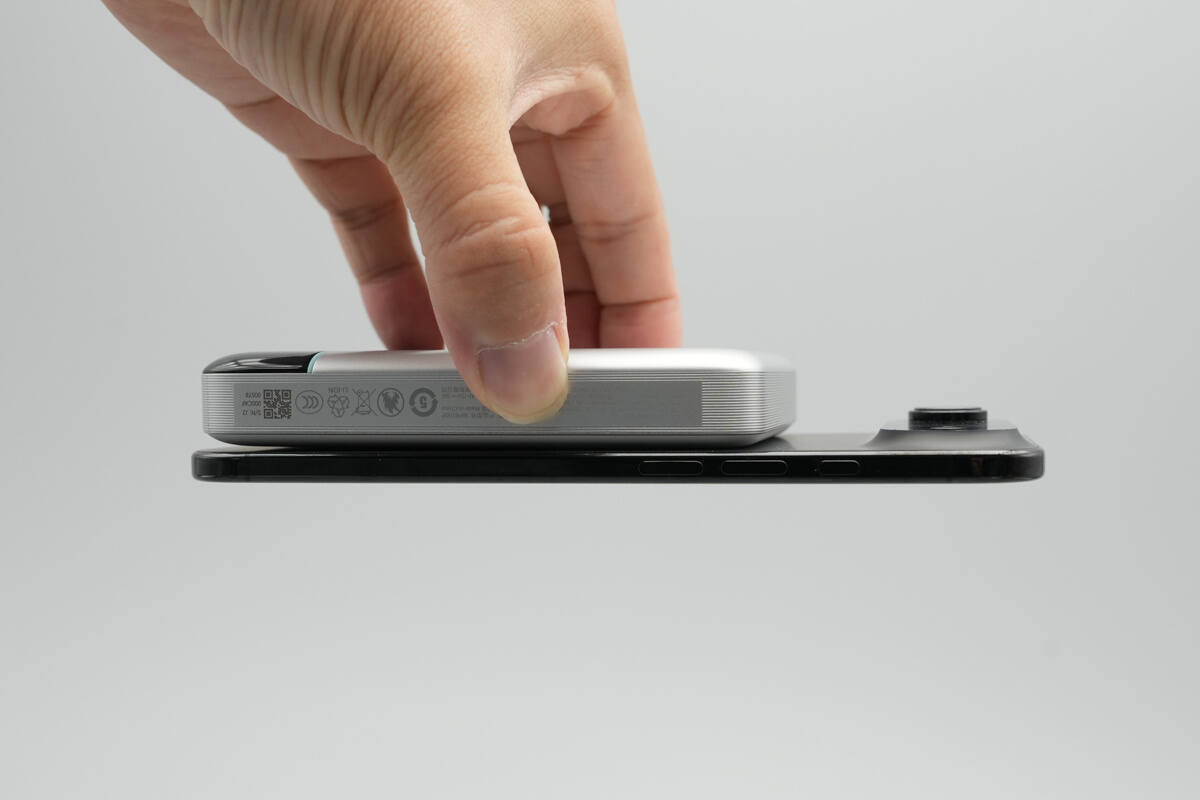
It can securely attach to the phone, holding it firmly without falling off.
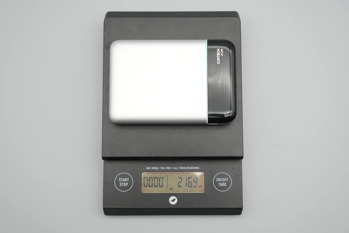
The weight is about 217 g (7.65 oz).
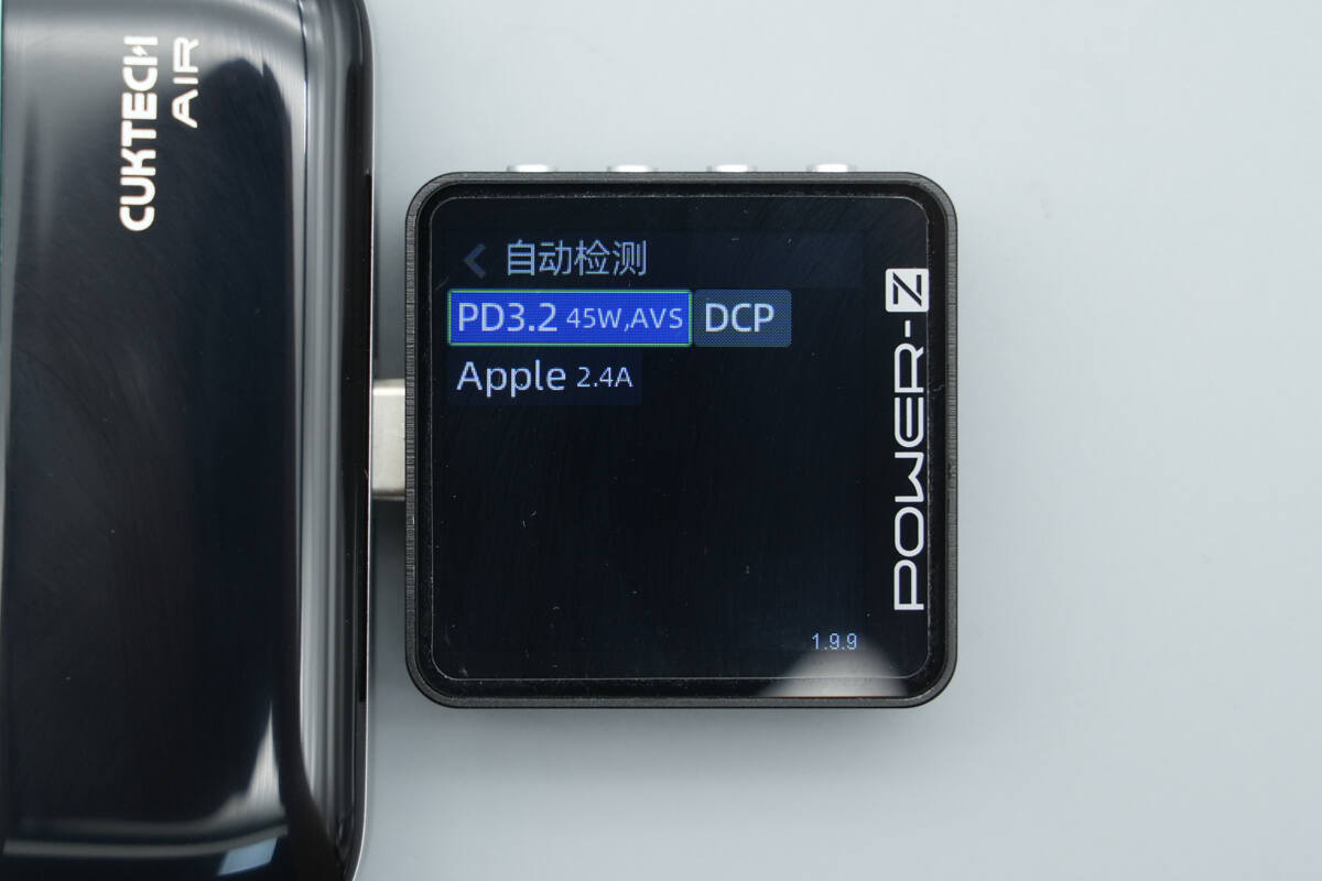
ChargerLAB POWER-Z KM003C shows that the USB-C port supports PD3.2, DCP, and Apple 2.4A charging protocols.
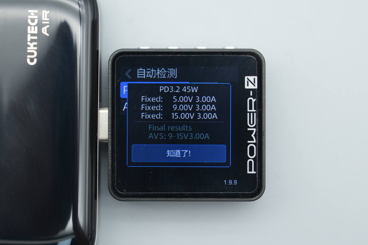
It has three fixed PDOs of 5V3A, 9V3A, and 15V3A, along with one set of SPR AVS voltage level, which is 9-15V3A.
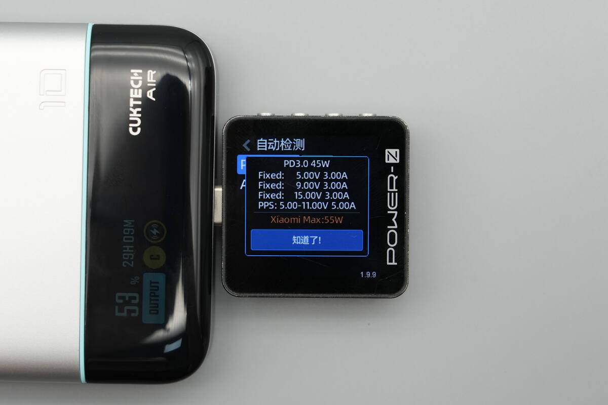
After switching the mode, it was also measured to support Xiaomi’s 55W proprietary Surge fast charging.
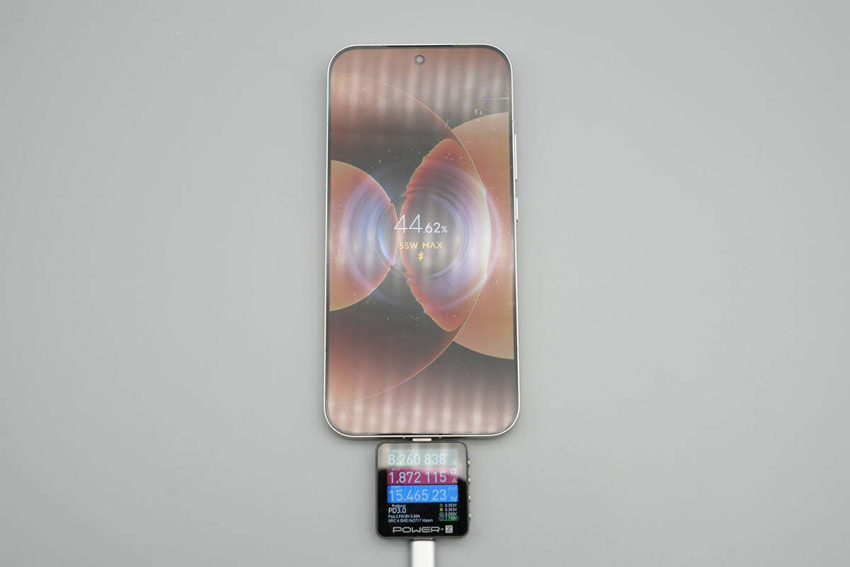
When charging the Xiaomi 17 Pro Max, it successfully activated Xiaomi’s 55W Surge fast charging.
Once the charging power stabilized, it was measured at 45.11 W.
Teardown
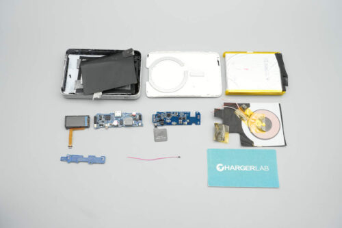
Next, let's take it apart to see its internal components and structure.
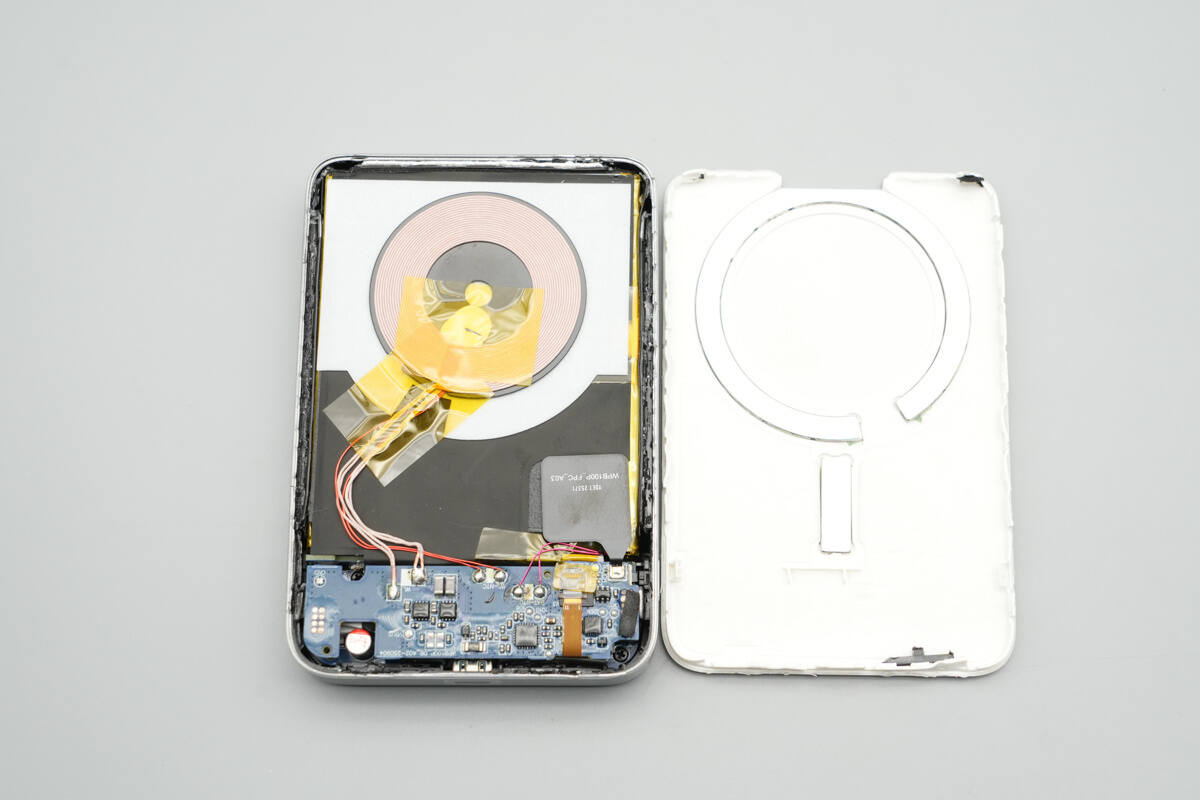
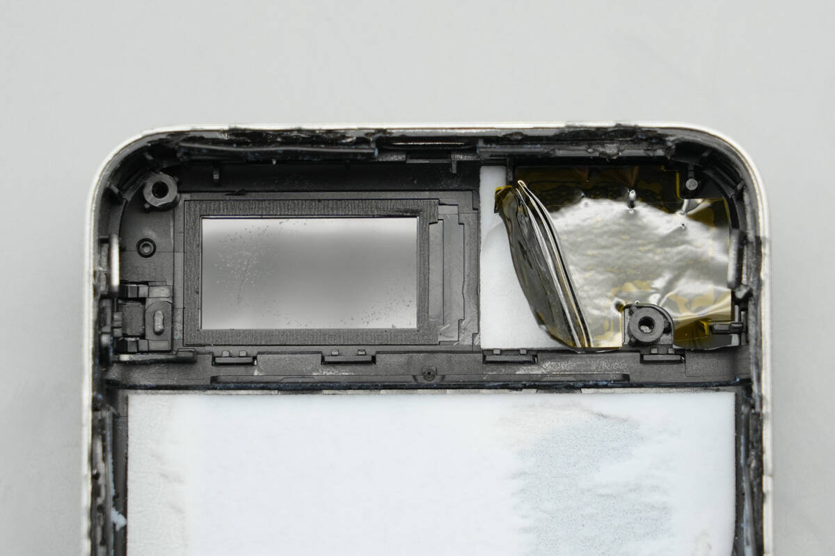
Remove the back casing. Revealing a magnetic ring and positioning magnets on the inner side. Fifteen high-performance N56 ultra-thin magnets provide stronger and more stable adhesion compared to traditional N52 magnets.
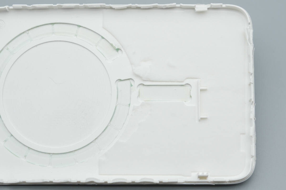
Thermal insulation padding is also attached.
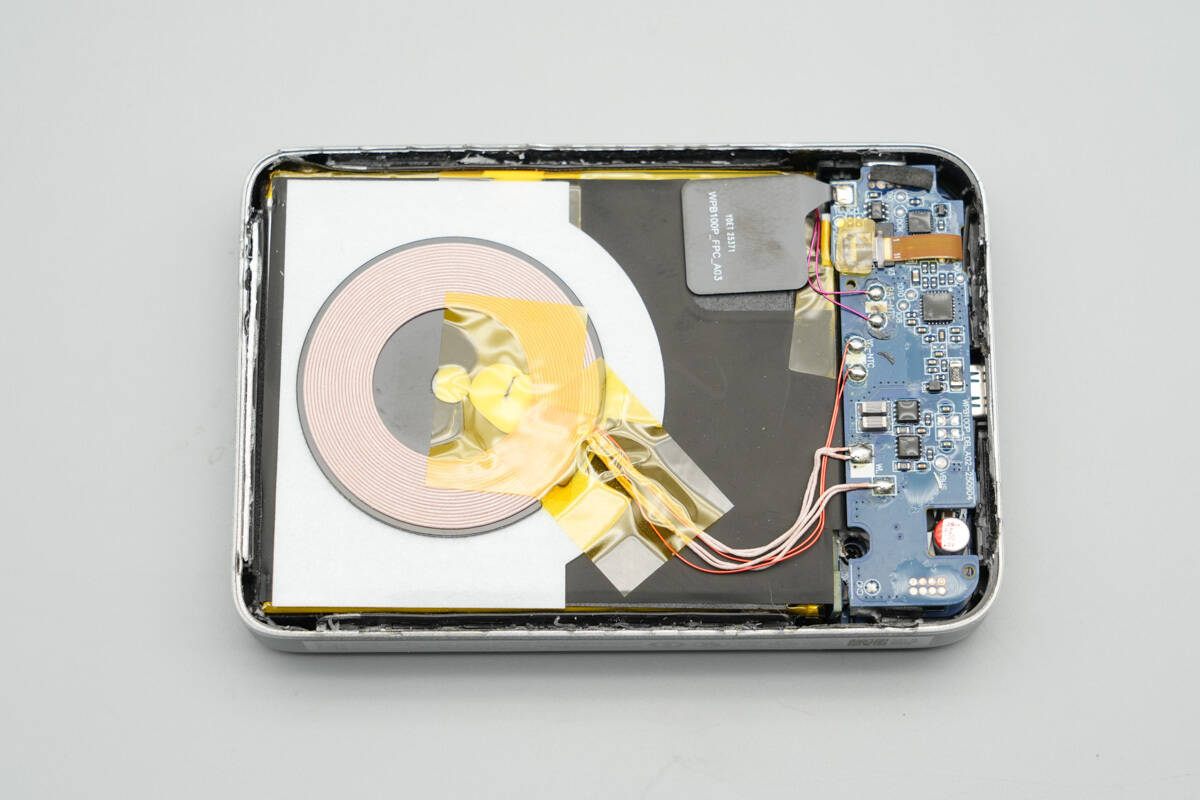
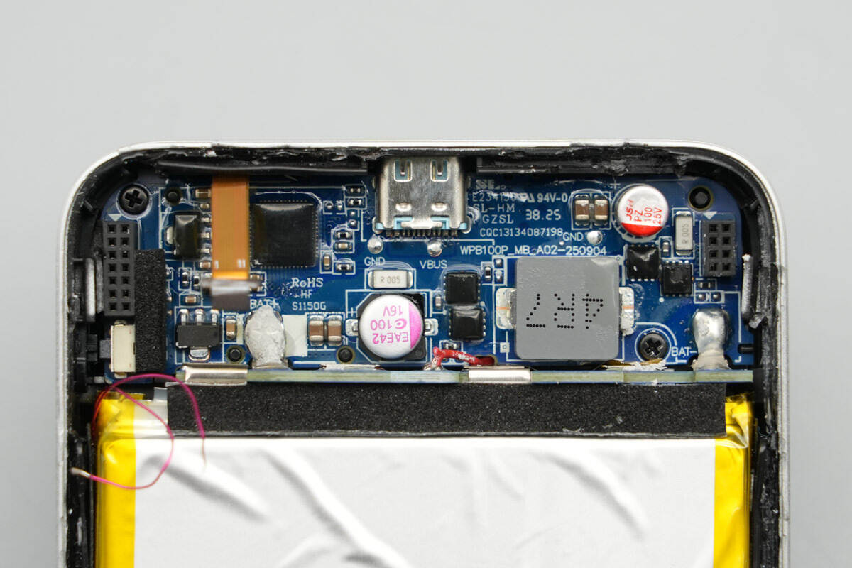
The wireless charging coil is positioned on top of the battery cell, with the PCBA module located on the right side.
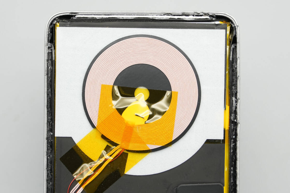
The charging coil is equipped with a thermistor for temperature monitoring and is secured with adhesive and tape. Below it, graphite thermal pads and foam are applied for heat dissipation.
The PCBA module features a self-developed U-shaped stacked design. The lower PCB is secured with screws, while the upper PCB connects the thermistor and wireless charging coil on its front side.
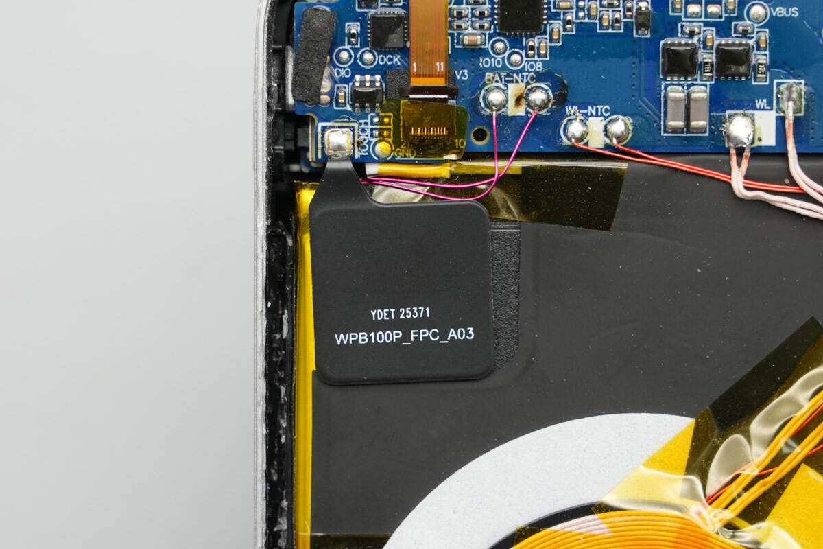
On the left side, electrodes for phone detection are soldered. The TFT high-definition display is connected to the PCB via a flex cable.
A thermal pad is placed between the two PCBs, along with insulating tape and adhesive for secure assembly.
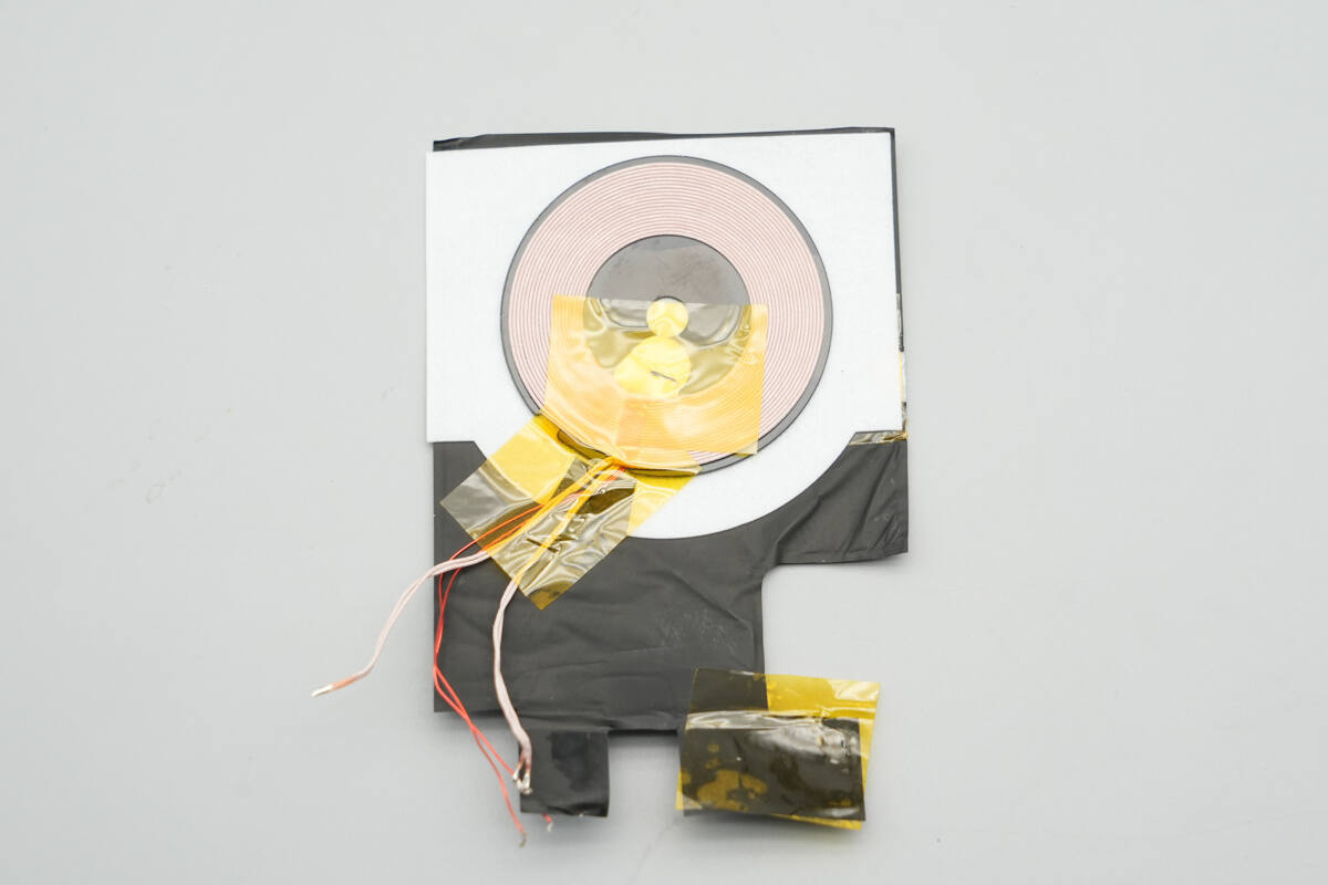
Remove the wireless charging coil.
The other side features a graphite thermal pad and a Mylar sheet.
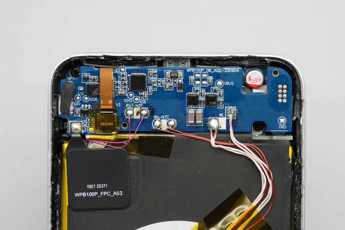
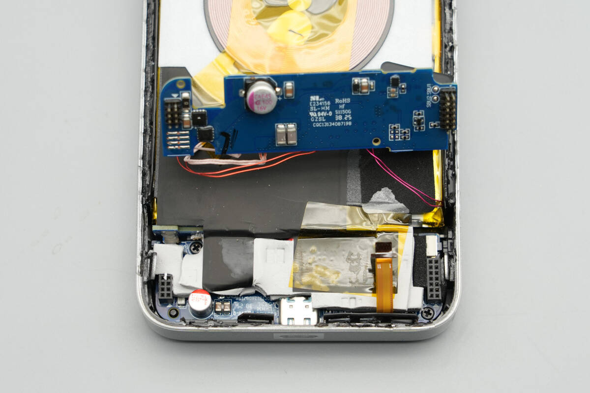
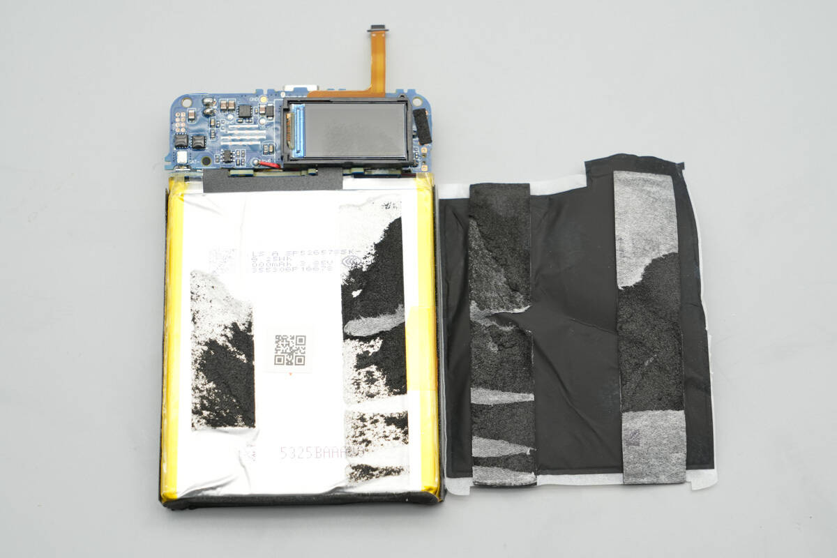
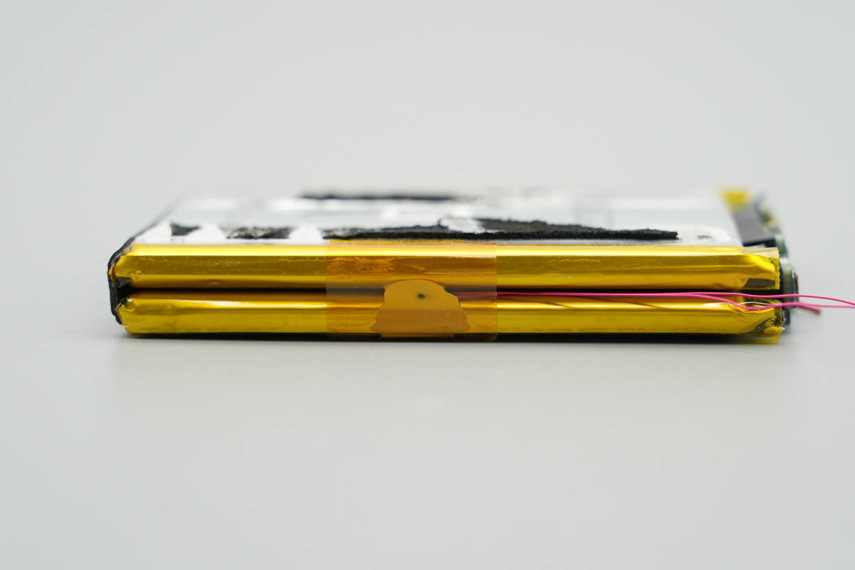
The battery pack’s nickel tabs are spot-welded to the lower PCB, with foam padding placed between the PCB and the battery cells.
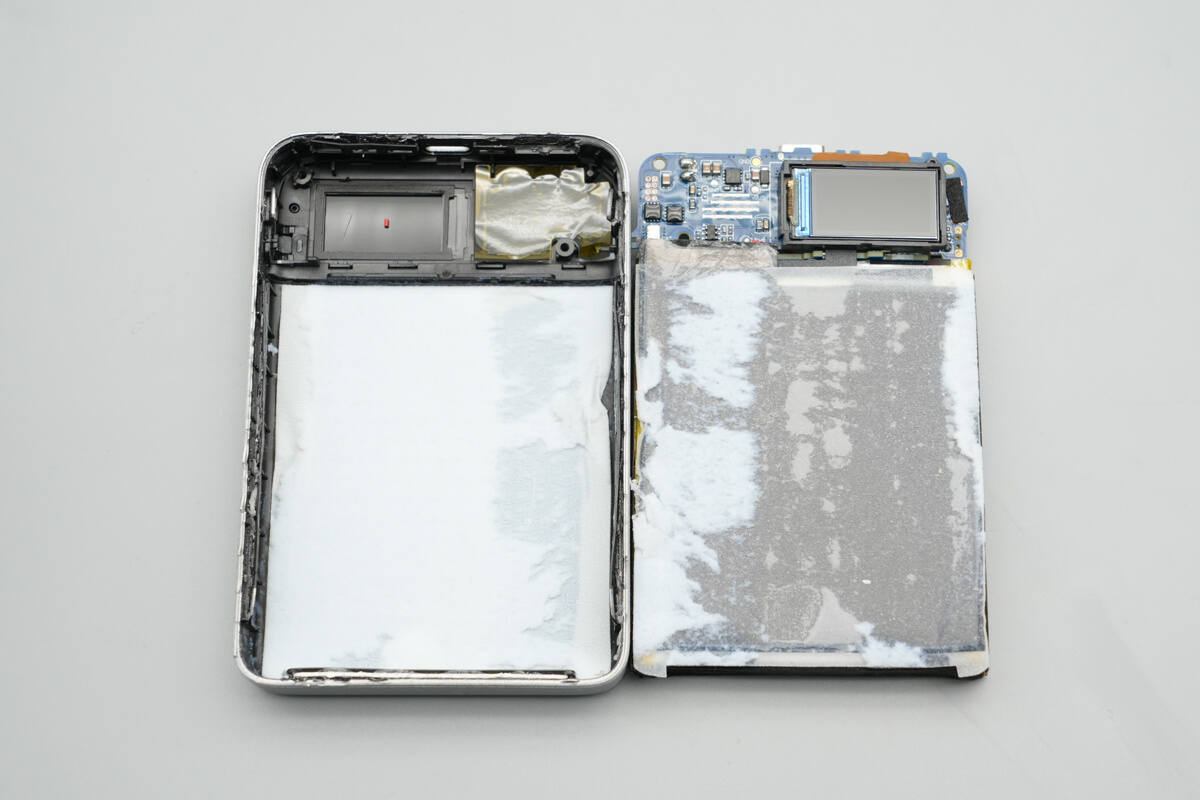
Remove the battery pack and PCB, revealing thermal insulation padding beneath the cells.
Sealing foam surrounds the display window, while thermal insulation and electrical insulation are applied on the right side.
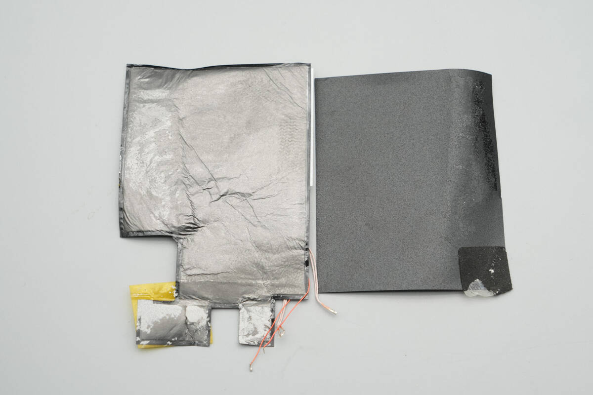
The other side of the battery pack is covered with a graphite thermal pad.
A thermistor is installed on this side.
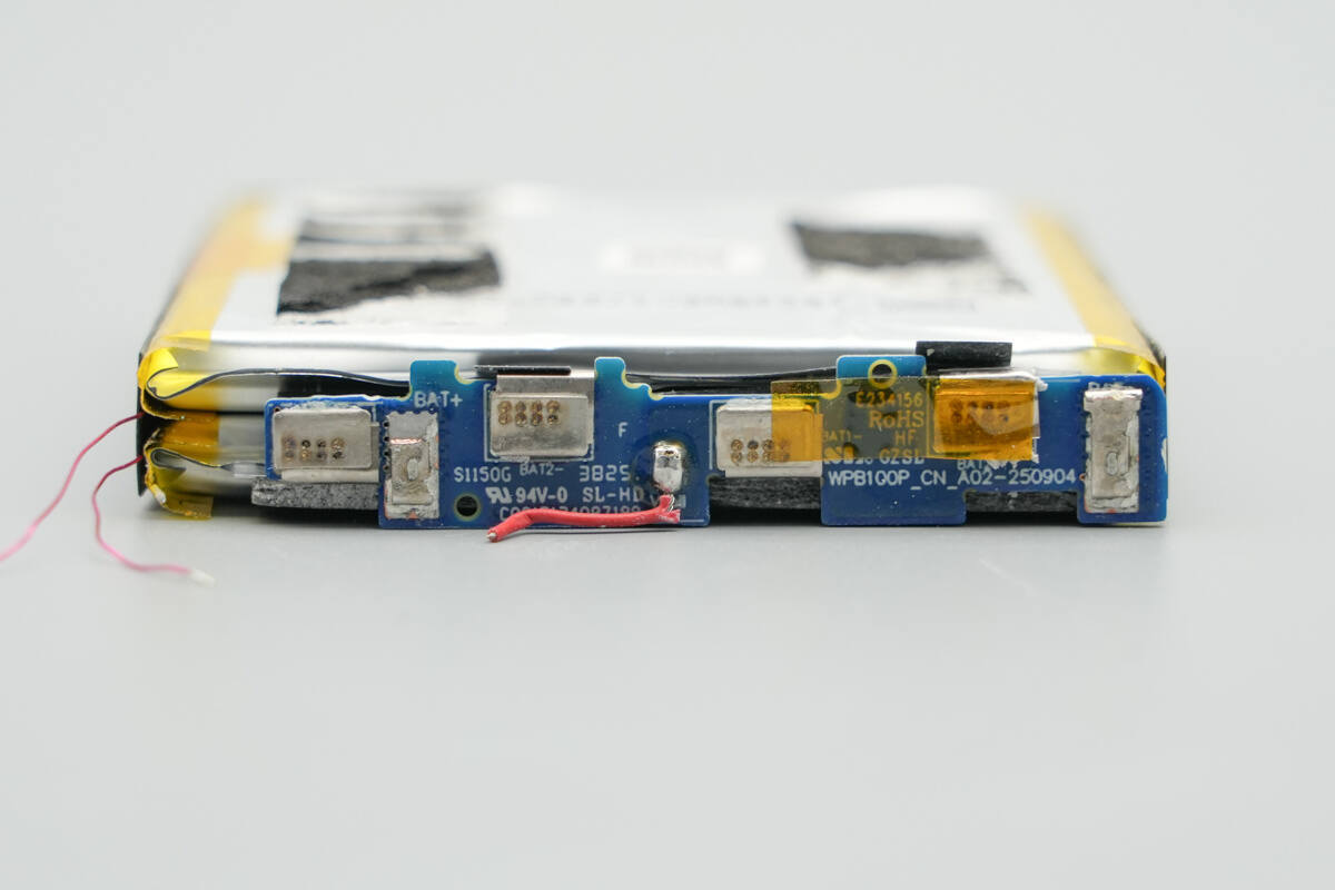
A small PCB is located at the top of the battery pack.
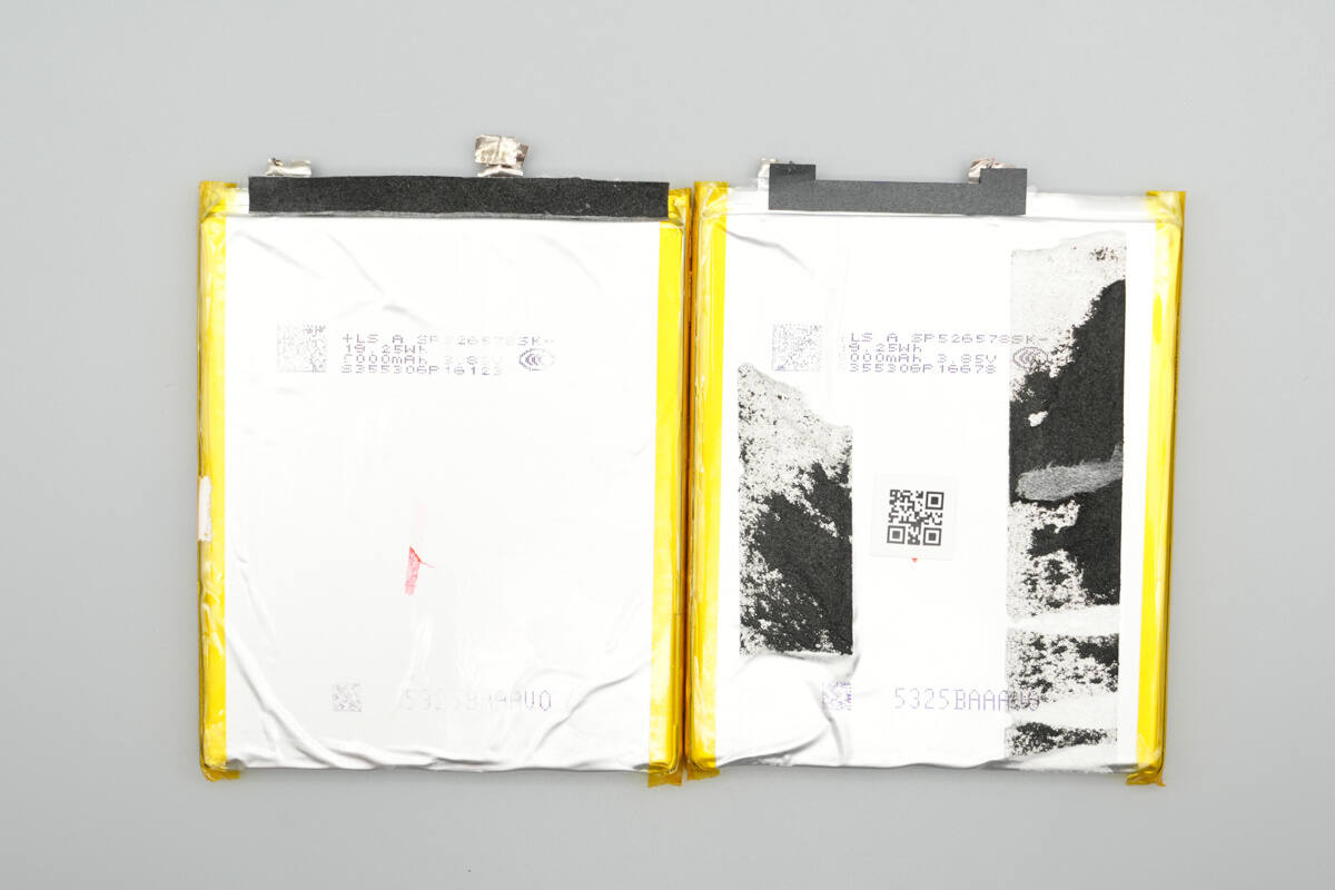
Separate the battery cells and the small PCB. Both cells are from LS, model SP526578SK, with a nominal voltage of 3.85 V, a capacity of 5000 mAh, and an energy rating of 19.25 Wh. They are CCC certified.
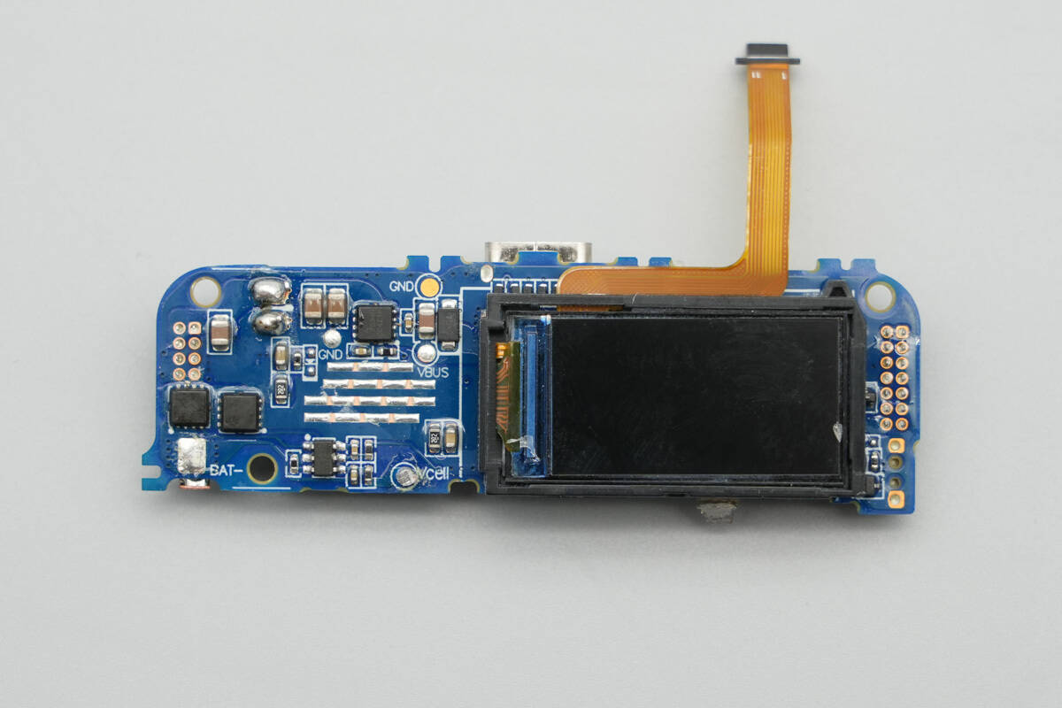
The display is secured and protected by a plastic frame. On the left side are the battery protection chip, battery protection MOSFETs, and the VBUS MOSFET.
On the other side of the PCB are the master control chip of the power bank, synchronous buck-boost MOSFETs, a buck-boost inductor, regulator chips, and solid capacitors, among other components.
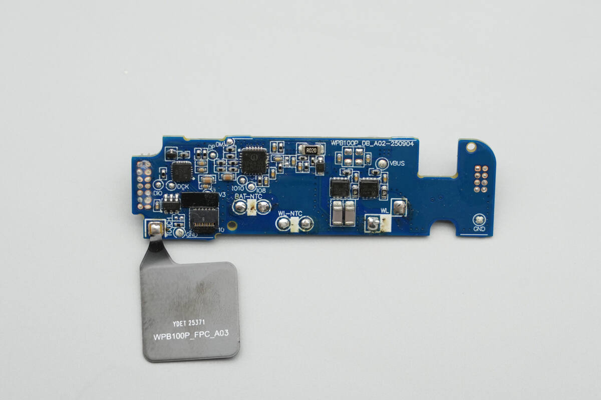
On the front side of the other PCB are the wireless charging master control chip, wireless charging power MOSFETs, MCU, touch controller, and other components.
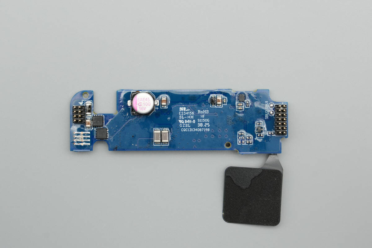
The back side houses VBUS MOSFETs, a solid capacitor, and NPO resonant capacitors, among other components.
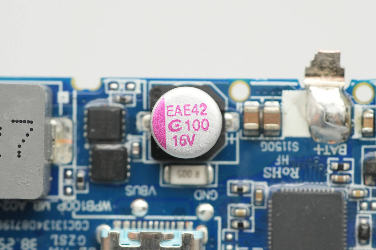
The battery-end solid capacitor is from APAQ, with a specification of 16 V, 100 μF.
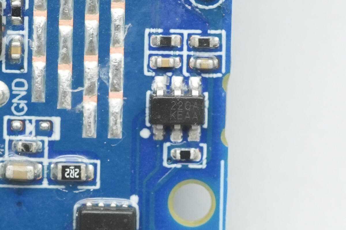
The battery protection chip is from iCM, marked “22QA,” model CM1025-QA. It is a protection IC designed for 2-series lithium/iron batteries, featuring high-precision voltage and current detection circuits. It supports monitoring for overcharge, over-discharge, overcurrent during discharge, short circuit, and overcurrent during charging.
Here is the information about iCM CM1025-QA.
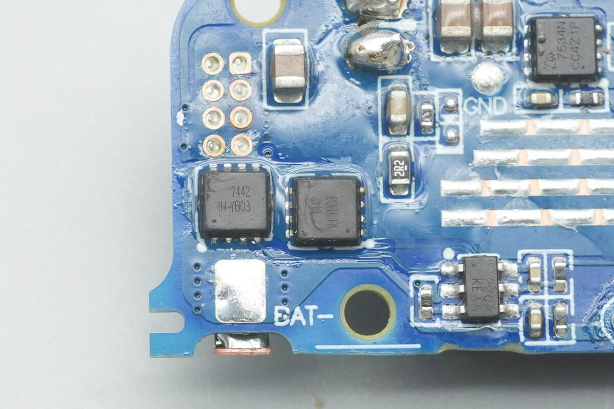
The battery protection MOSFETs are marked “7442” and use a DFN 3×3 mm package.
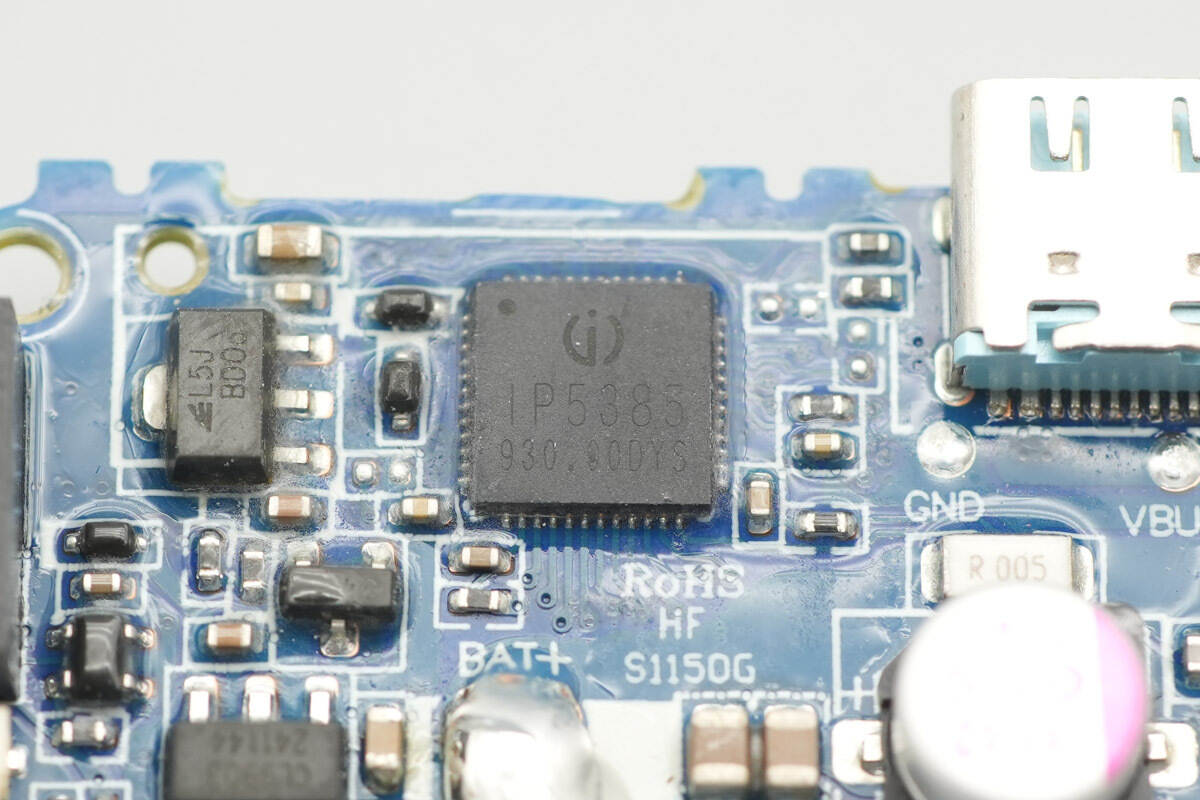
The master control chip of the power bank is from Injoinic, model IP5385. It is the first mobile power SOC integrating the UFCS protocol. It supports multiple fast-charging protocols: QC2.0/QC3.0, SCP, UFCS for output; AFC/FCP for input and output; Type-C PD2.0/PD3.0 for input and output; Type-C PD3.0 PPS for output; and BC1.2 for Apple devices. It features a synchronous bidirectional buck-boost converter, lithium battery charging management, battery level indication, and other functions, providing a complete power management solution for fast-charging power banks.
The IP5385 can simultaneously support two USB-A ports, one USB-C port, and one Lightning port. Each port individually supports fast charging. When two or more output ports are used simultaneously, only a 5V input/output is supported. Thanks to the high integration and rich functionality of the IP5385, very few external components are required for the application; a single inductor is sufficient to achieve bidirectional buck-boost conversion, effectively reducing overall design size and lowering BOM costs.
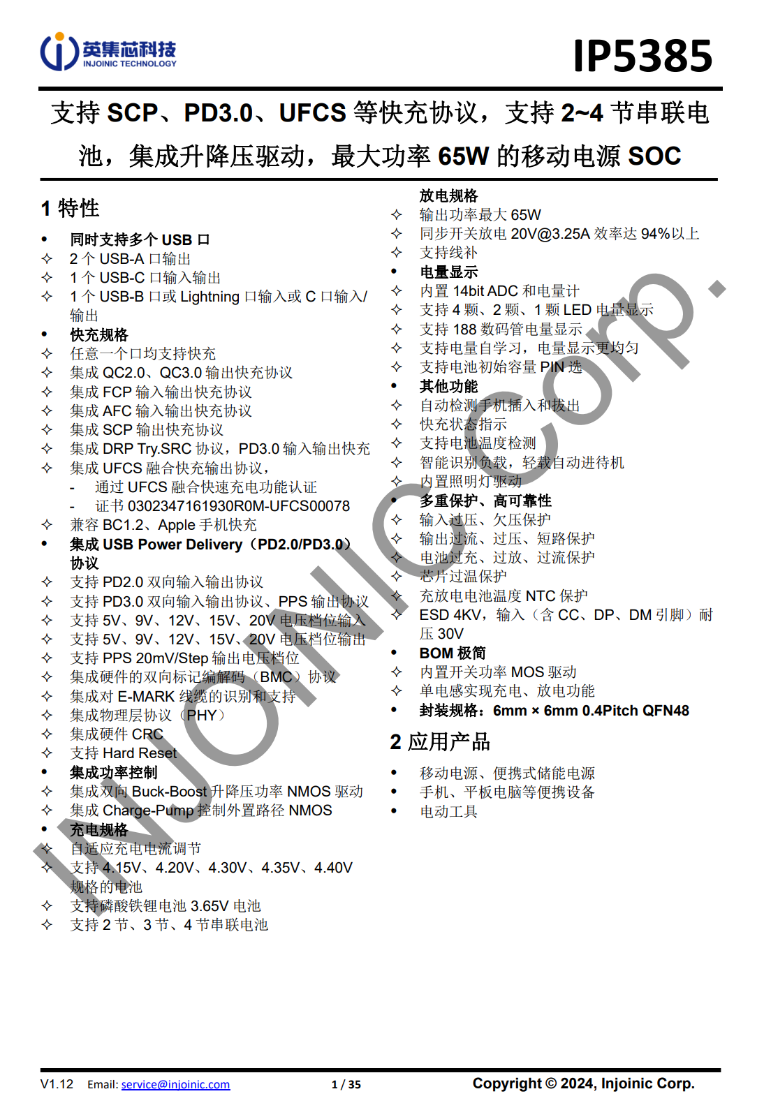
The IP5385 supports 2–4 series-connected battery cells, and its synchronous buck-boost system can provide up to 65 W of input and output power. It automatically enters sleep mode under light loads.
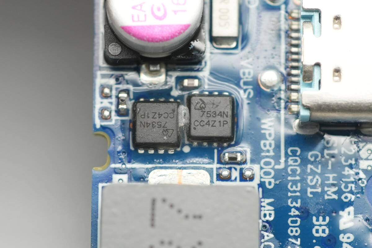
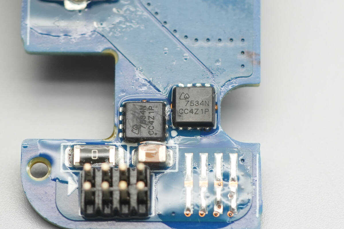
The synchronous buck-boost MOSFETs are from AOS, model CQY7534N. They are NMOS devices with a voltage rating of 30 V and an on-resistance of 4.8 mΩ, packaged in a DFN 3×3 mm EP package.
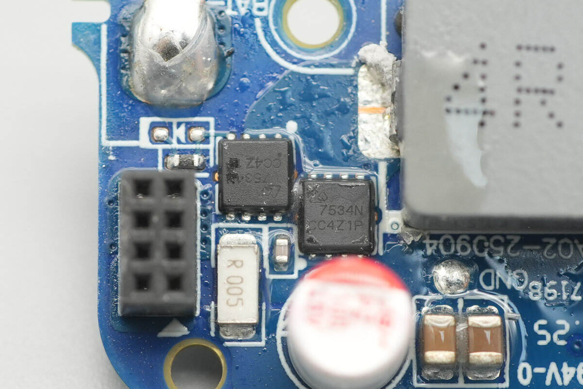
A close-up of the other two AOS CQY7534N synchronous buck-boost MOSFETs.
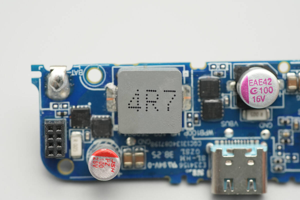
A close-up of the 4.7 μH buck-boost inductor.
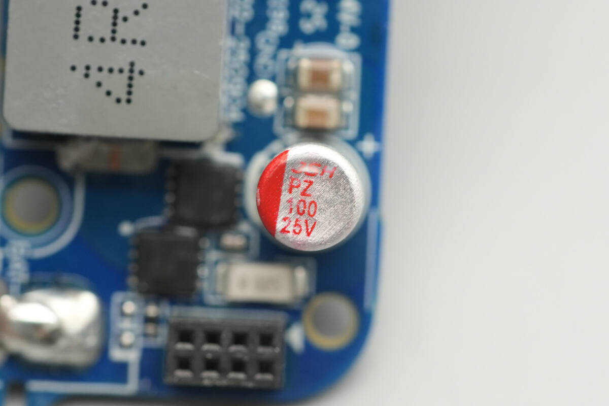
This solid capacitor is from JSH, with a specification of 25 V, 100 μF.

The USB-C port VBUS MOSFET also uses the AOS CQY7534N.
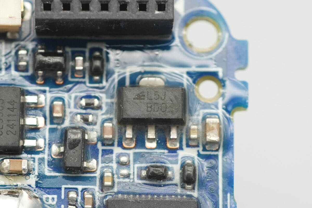
Close-up of a regulator chip marked with “L5J.”
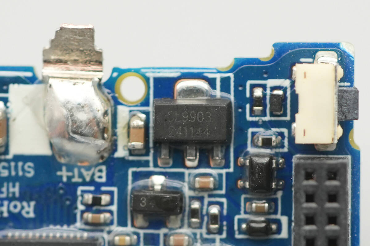
A close-up of another regulator chip marked “CL9903.”
The VBUS MOSFET used to control wireless charging power also uses the AOS CQY7534N.
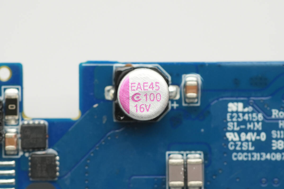
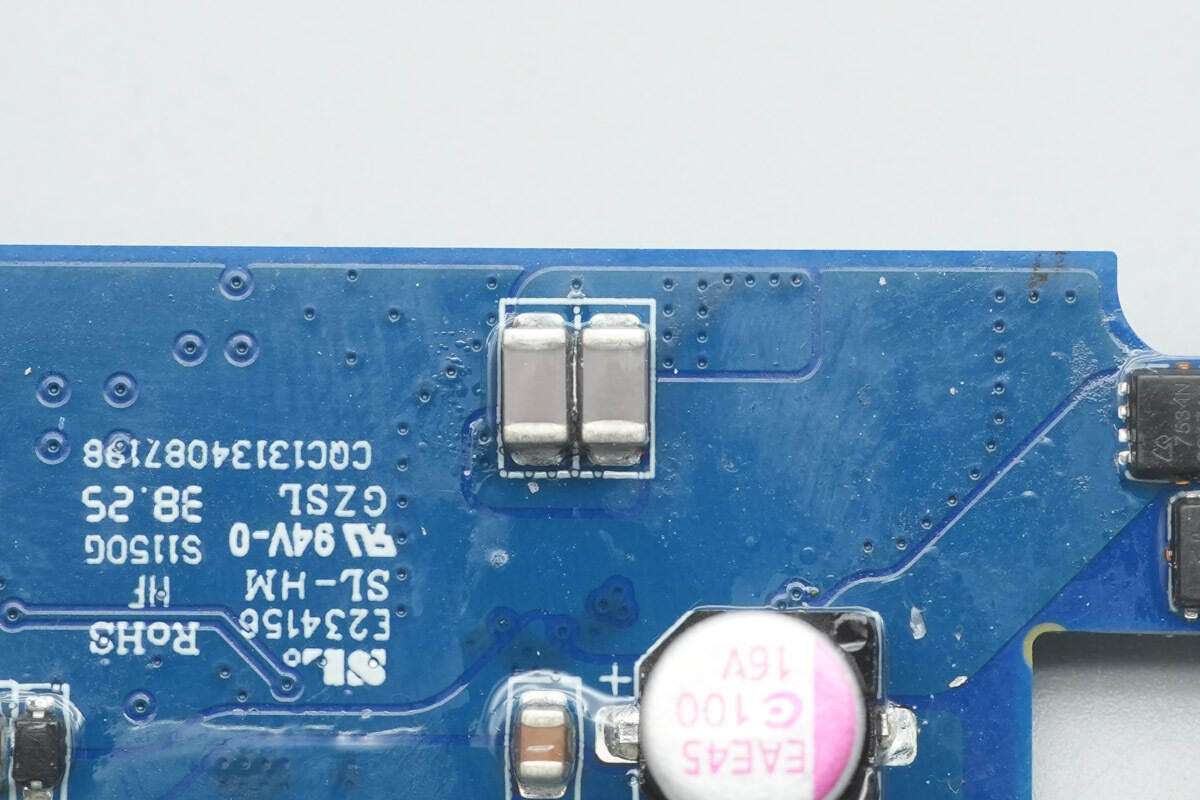
This solid capacitor is also from APAQ, with a specification of 16 V, 100 μF.

The wireless charging master control chip is from Injoinic, model IP6823. It is a highly integrated wireless charging transmitter controller compliant with the WPC Qi standard. It integrates an H-bridge driver module, an ASK communication demodulation module, and necessary resources for adapter fast-charging Sink protocols.
The chip supports protocol customization, foreign object detection sensitivity, indicator light functions, and more. It comes in a QFN24 package, with pin functions optimized for wireless charging applications, making PCB layout design straightforward.
Here is the information about Injoinic IP6823.
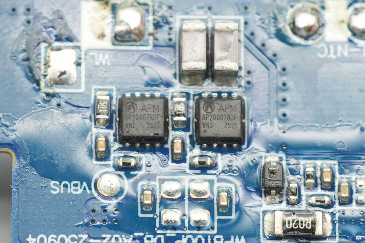
The wireless charging power MOSFETs are from APM, model AP20G02BDF. They are N+P dual MOSFETs designed for full-bridge wireless charging applications. The NMOS has a voltage rating of 20 V and an on-resistance of 12 mΩ, while the PMOS has a voltage rating of –20 V and an on-resistance of 25 mΩ. They are packaged in a PDFN 3×3 mm 8L package.
A close-up of the two NPO resonant capacitors.
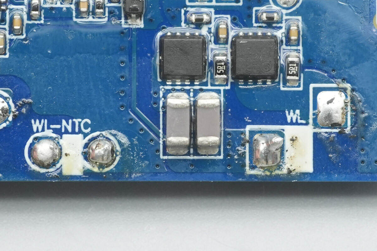
The other two NPO resonant capacitors are located on the opposite side of the PCB.
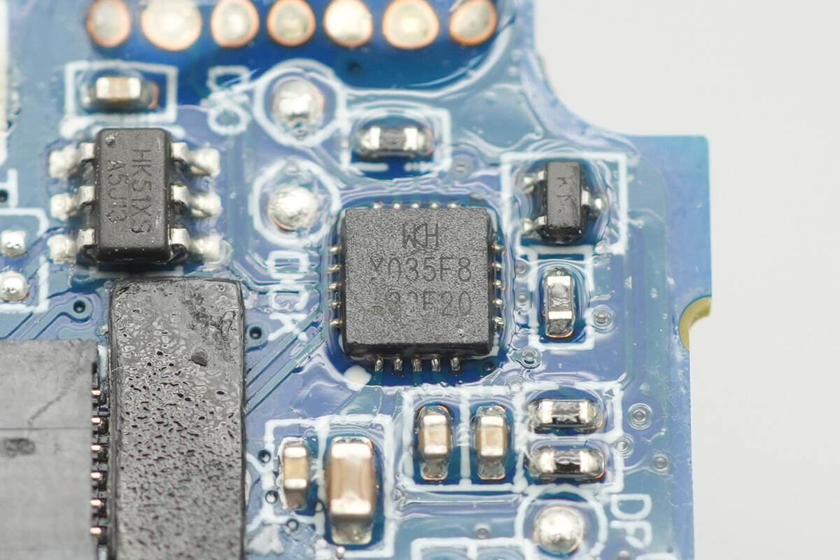
The MCU driving the display is from WCH, model CH32X035F8U6. It is based on a RISC-V core and features 62 KB of flash memory and 20 KB of RAM. It also integrates an ADC, operational amplifier, USB, and PD physical layer.
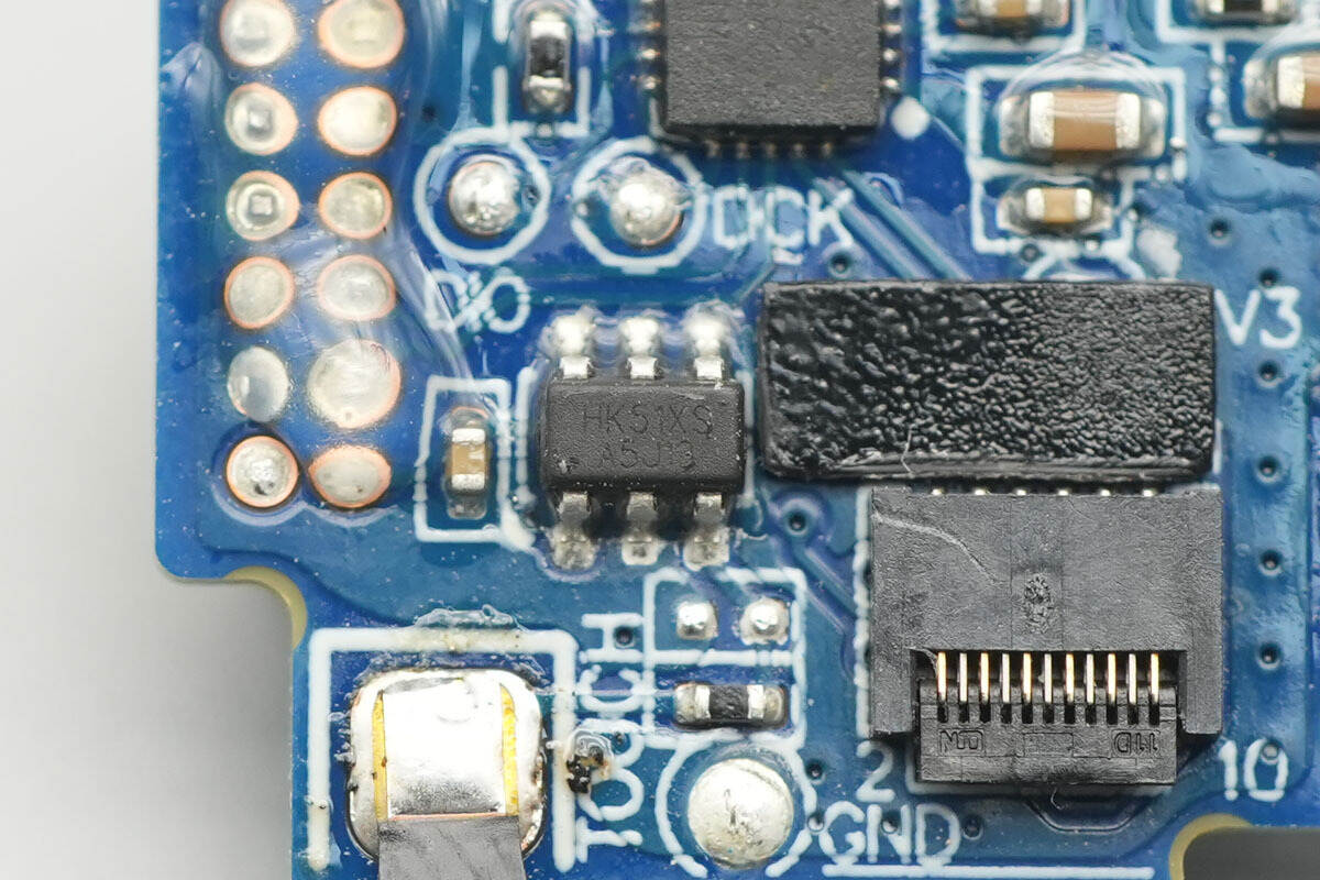
The touch controller chip is marked “HK51XS” and comes in an SOT23-6 package.
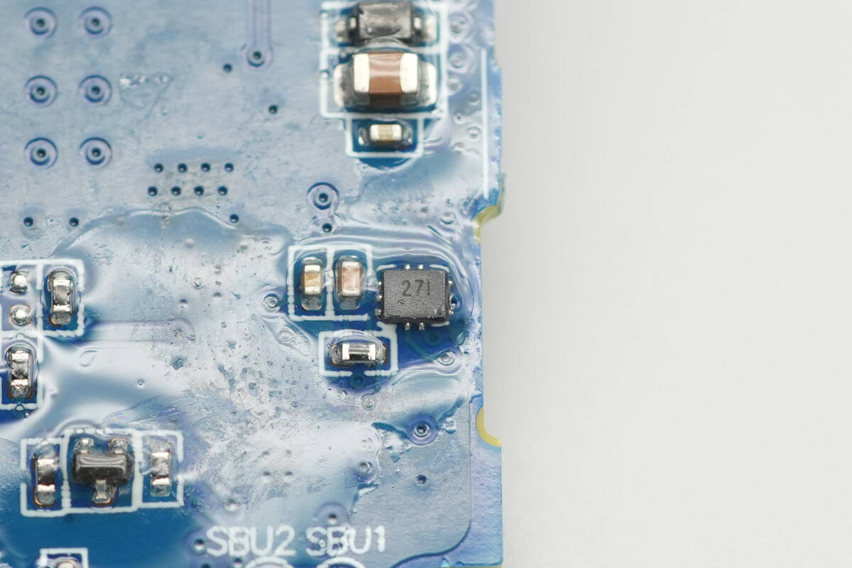
A toggle switch marked “27I.”

Well, those are all components of the CUKTECH 10 Super Magnetic Power Card.
Summary of ChargerLAB
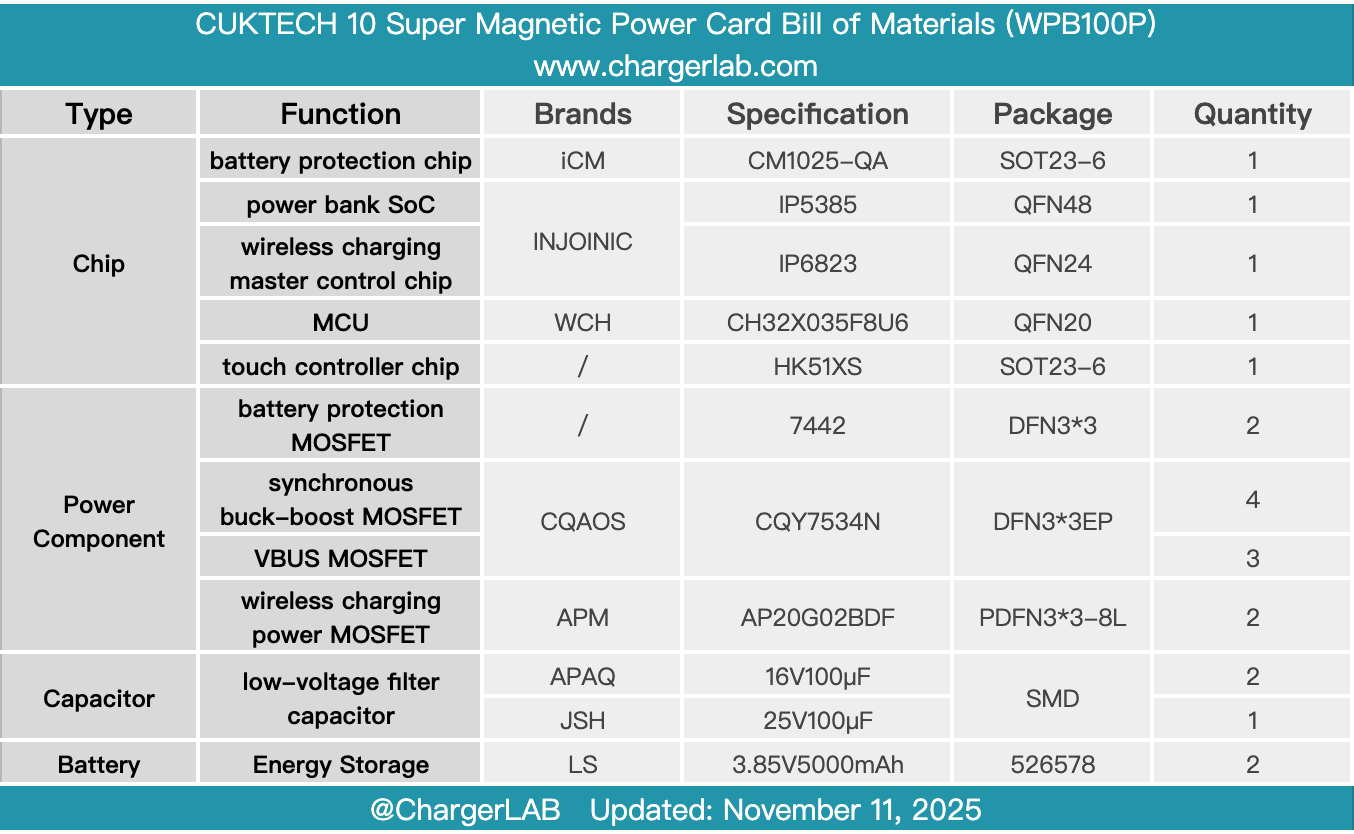
Here is the component list of the CUKTECH 10 Super Magnetic Power Card for your convenience.
The body features a painted finish, with the back made of liquid silicone. The high-definition display provides a rich interface, visualizing battery level, input/output parameters, and more. The power bank is compatible with PPS, MIPPS, PD, and other fast-charging protocols, supporting up to 55 W bidirectional wired fast charging as well as 15 W wireless charging. Its 10,000 mAh capacity meets daily usage needs.
After taking it apart, we found that it uses a next-generation silicon–carbon anode battery jointly developed and customized by CUKTECH and LS, with each cell as thin as 0.52 cm. It is equipped with an iCM CM1025-QA battery protection chip and a thermistor for temperature control and protection against overcharge and over-discharge.
The PCBA module is composed of a dual-layer stacked PCB. It uses the Injoinic IP5385 SOC for bidirectional fast-charging control and the Injoinic IP6823 for wireless charging management. High-performance N56 ultra-thin magnets are built in, providing stronger and more stable adhesion compared to traditional N52 magnets. Graphite thermal pads are applied to both sides of the battery cells, and a thermal pad is placed within the PCB layers. The coil is also equipped with a thermistor for temperature monitoring, ensuring reliable construction.
Related Articles:
1. Teardown of UGREEN Nexode 160W 5-Port GaN Charger (X774)
2. Teardown of Xiaomi 67W 20000mAh Power Bank with Integrated Cable (PB2067)
3. Teardown of HONOR 80W SuperCharge Wireless Charger Stand (Power-W06)