Introduction
CANDYSIGN has launched a 160W CoCan Ultra featuring a modular design that combines an extension power strip and a portable charger, enabling seamless switching between home and travel use.
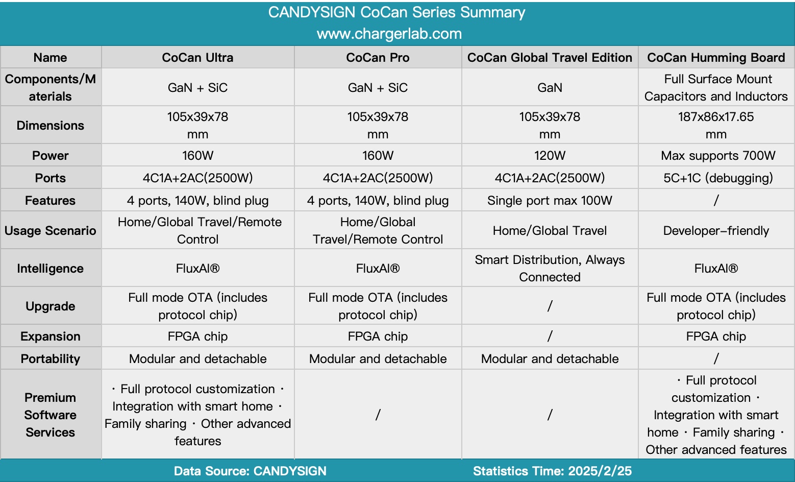
Building on the excellent design of the CoCan series, the performance has been comprehensively upgraded to support 140W PD3.1 fast charging and UFCS hybrid fast charging. With four USB-C ports and one USB-A port, the total output can reach up to 160W. In addition, it introduces for the first time the CoCan CanOS system, the new FluxAI® technology, and full-model OTA capability, making it extremely powerful. Now, let’s take a closer look at the internal design and components.
Product Appearance
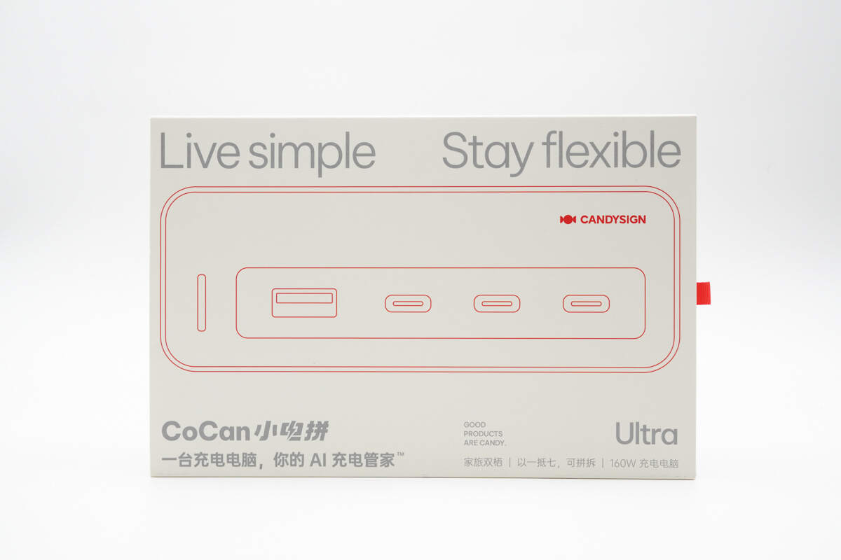
The packaging features a drawer-style design, with the top printed with a simplified front view of the product, a slogan, and key selling points.
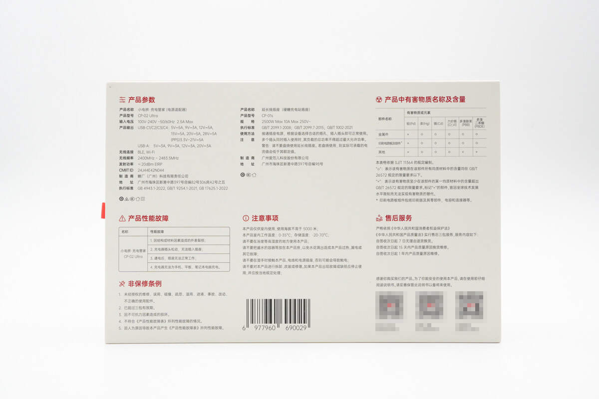
The bottom of the box displays product specifications, safety notices, and after-sales service information.
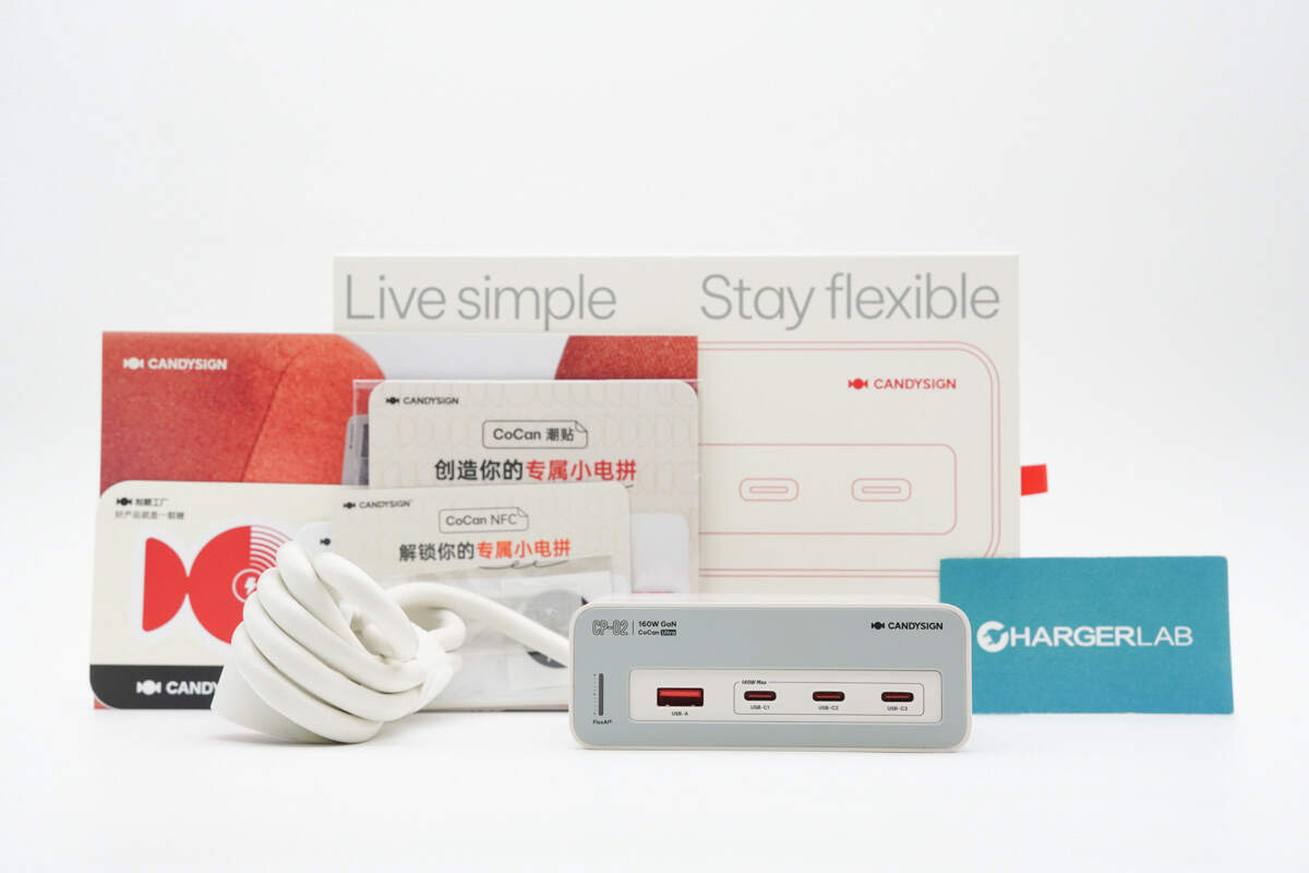
The package includes the charger and some documents.
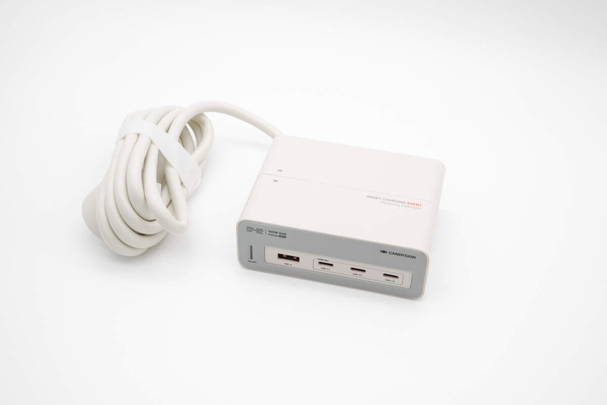
It features a retro light gray color and a finely textured finish, with a housing made from high flame-retardant materials.
It adopts a modular AC+DC design with foldable prongs, allowing the two units to be combined or detached as needed. The unique structure enables it to function as both a desktop charger and a power strip.
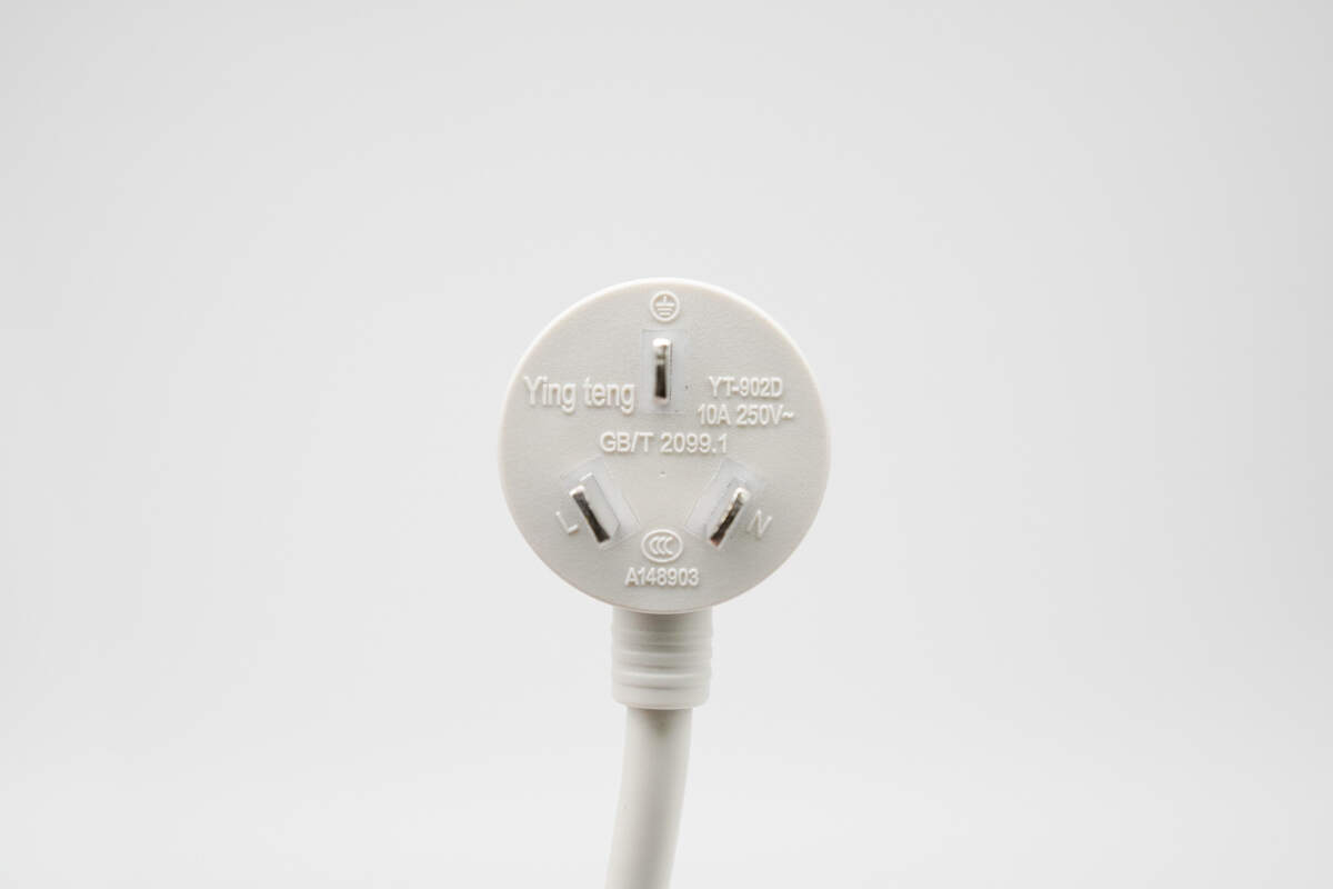
The input plug is rated at 10A 250V\~ and is CCC certified.
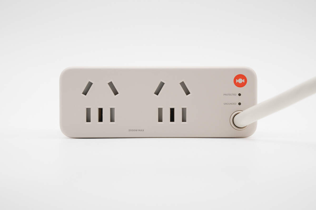
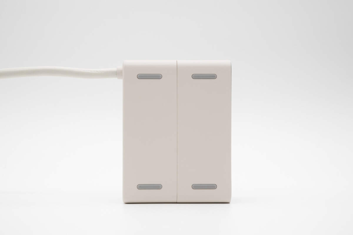
The connection at the power cord is reinforced with a protective rubber sleeve. It features two sets of Chinese standard 5-hole sockets, with the logo printed on the right side alongside two indicator lights.
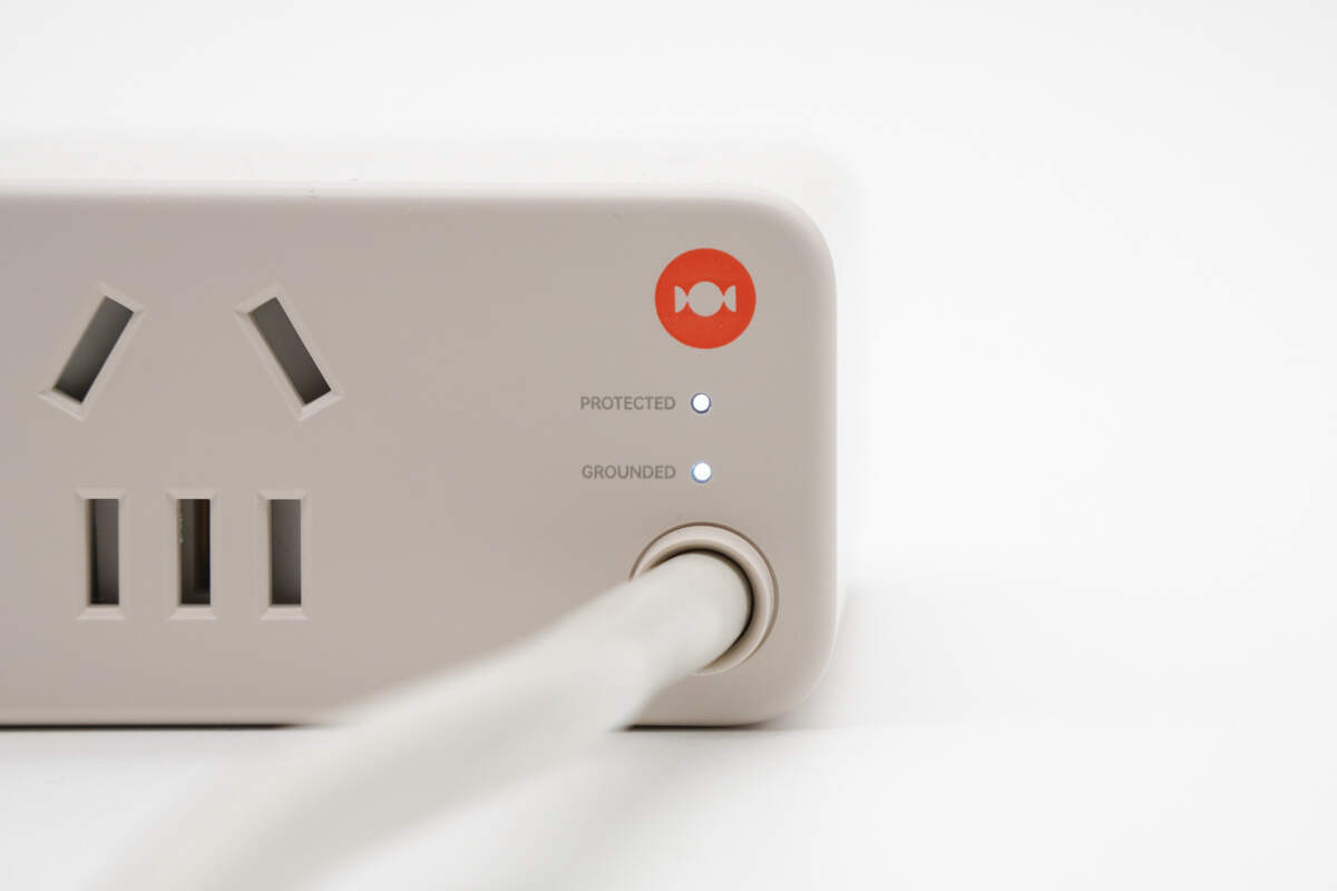
The socket is equipped with built-in safety shutters to prevent foreign objects from being inserted. It features two indicator lights: one for surge protection and one for grounding protection. Under normal operation, both indicators emit a white light.
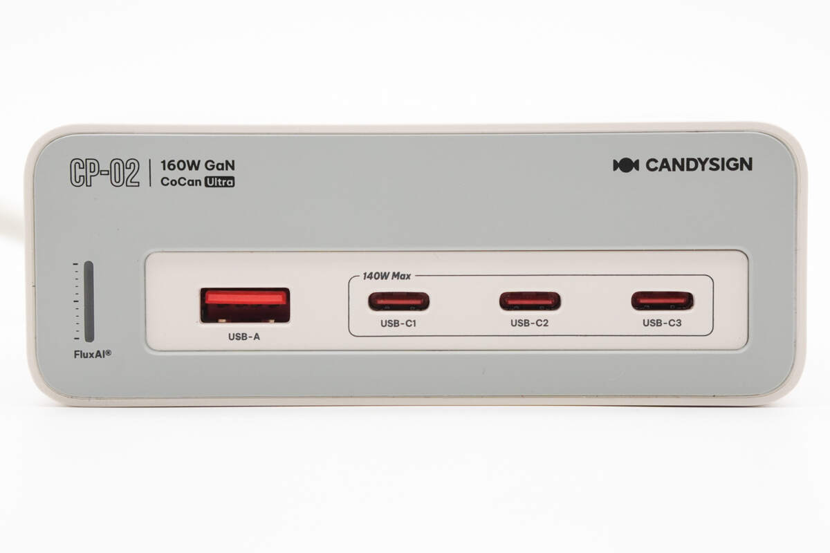
The front is labeled with the model number of this module: CP-02. It features three USB-C ports and one USB-A port, with an energy bar indicator light on the left side.
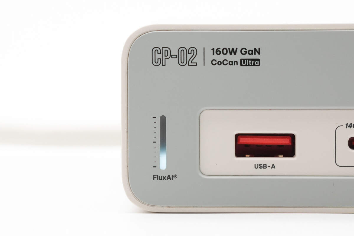
The indicator lights white when powered on, and rises progressively with increasing load power.
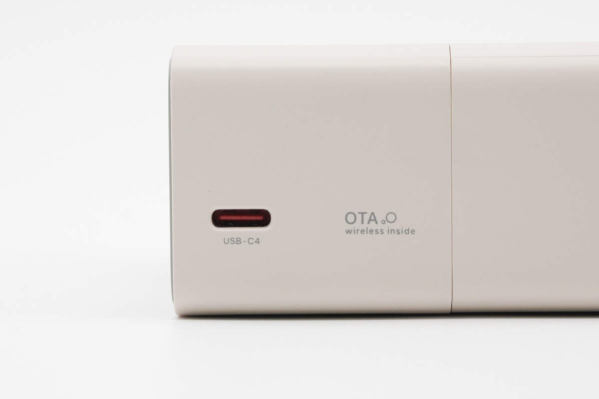
The USB-C4 port is on the side, with “OTA Wireless Inside” printed next to it.
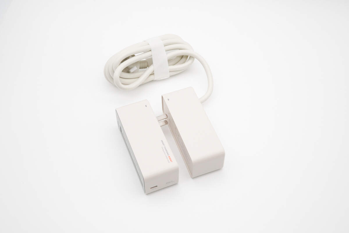
Both modules have anti-slip pads on the bottom.
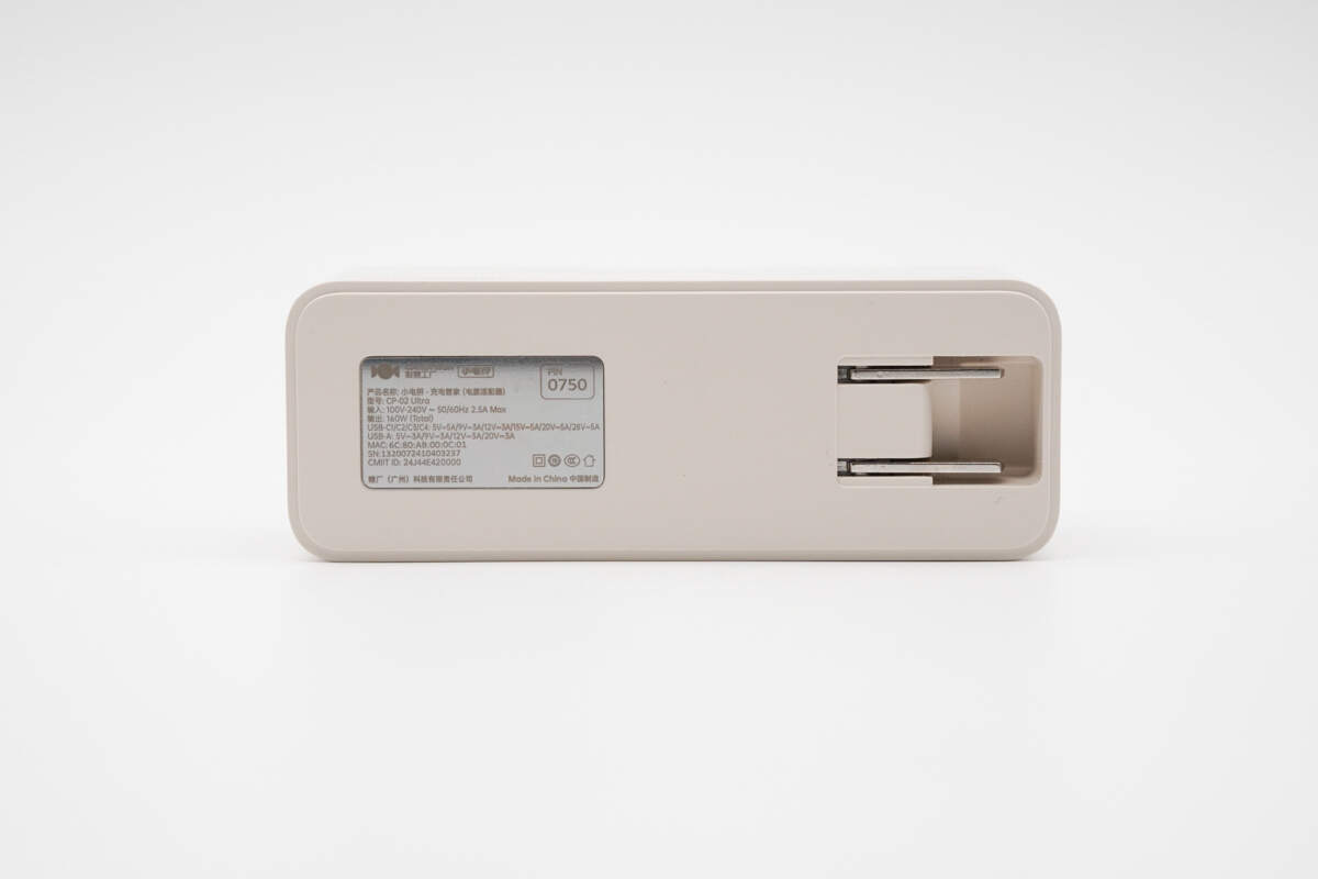
The input end of the charger module features prongs on one side and a nameplate on the other.
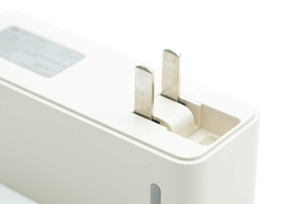
The prongs are foldable for convenient storage and portability.
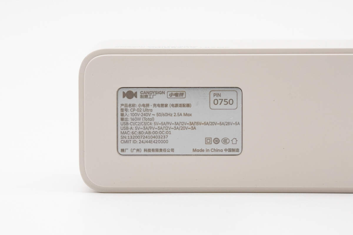
Model: CP-02 Ultra
Input: 100-240V\~ 50/60Hz 2.5A Max
Output: 160W (Total)
USB-C1/C2/C3/C4: 5V⎓5A, 9V⎓3A, 12V⎓3A, 15V⎓3A, 20V⎓5A, 28V⎓5A
USB-A: 5V⎓3A, 9V⎓3A, 12V⎓3A, 20V⎓3A
CCC Certified
When the two modules are separated, the front socket on the extension module can be used to power an electrical device.
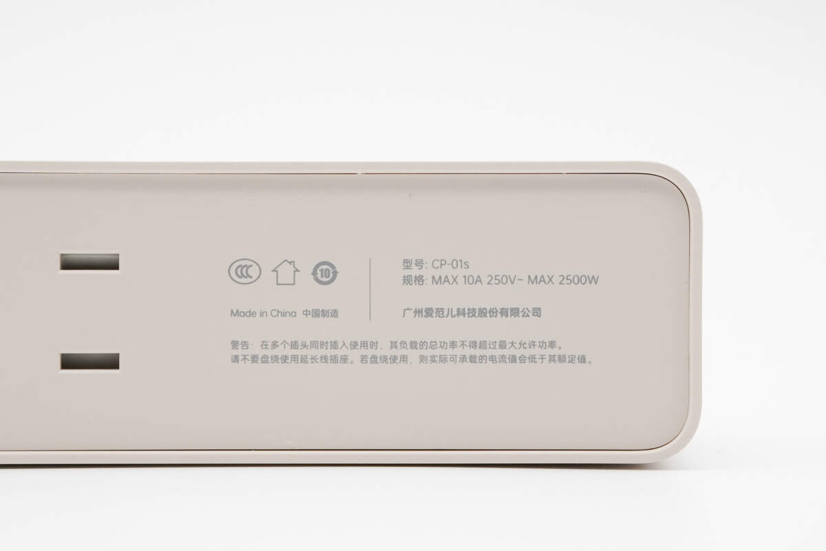
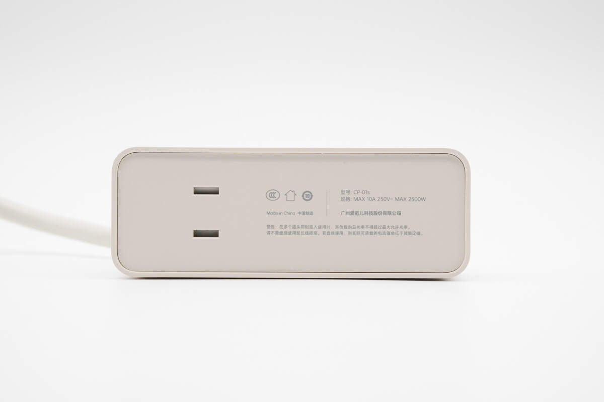
The housing is printed with the module model number CP-01s, along with technical specifications and warning information.
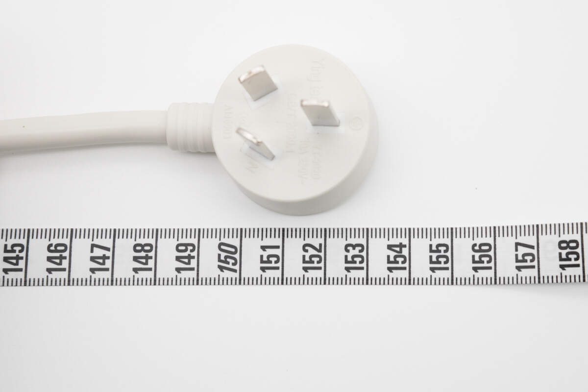
The length of the power cord is about 153 cm (60.24 inches).
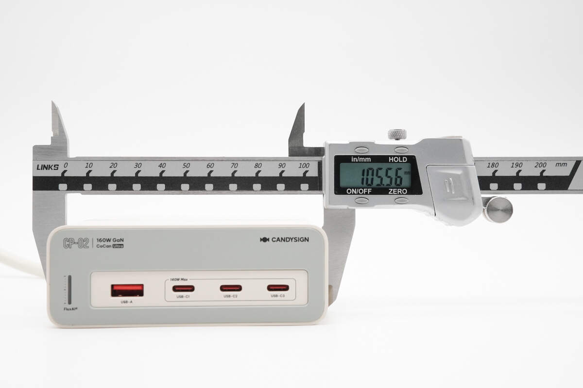
The length of the charger is about 105.56 mm (4.16 inches).
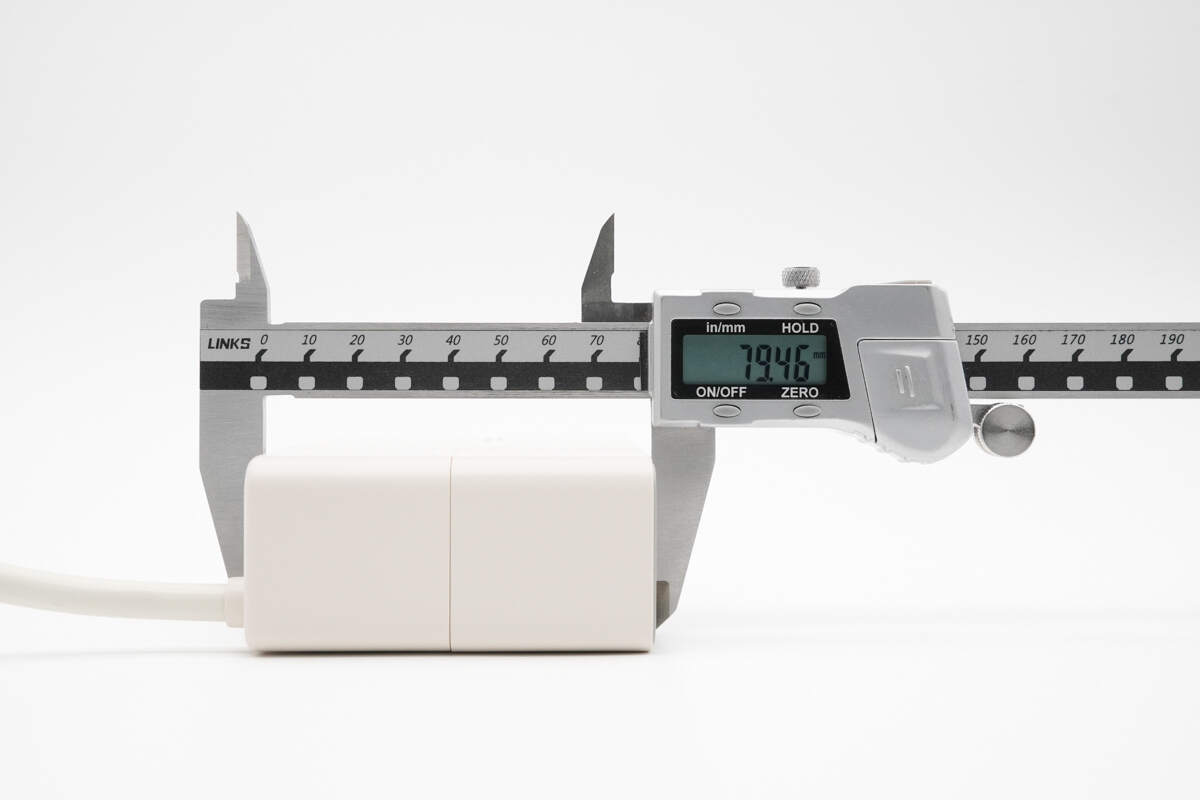
The width is about 79.46 mm (3.13 inches).
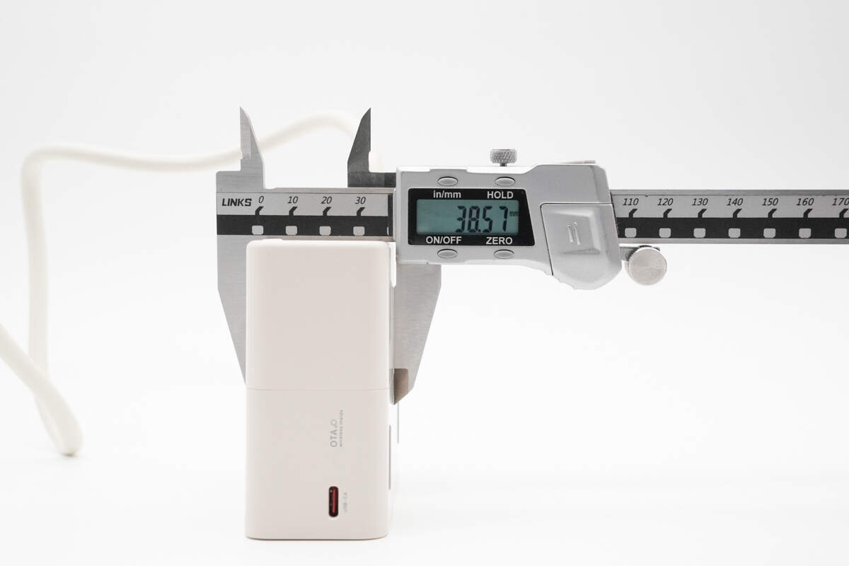
The thickness is about 38.57 mm (1.52 inches).
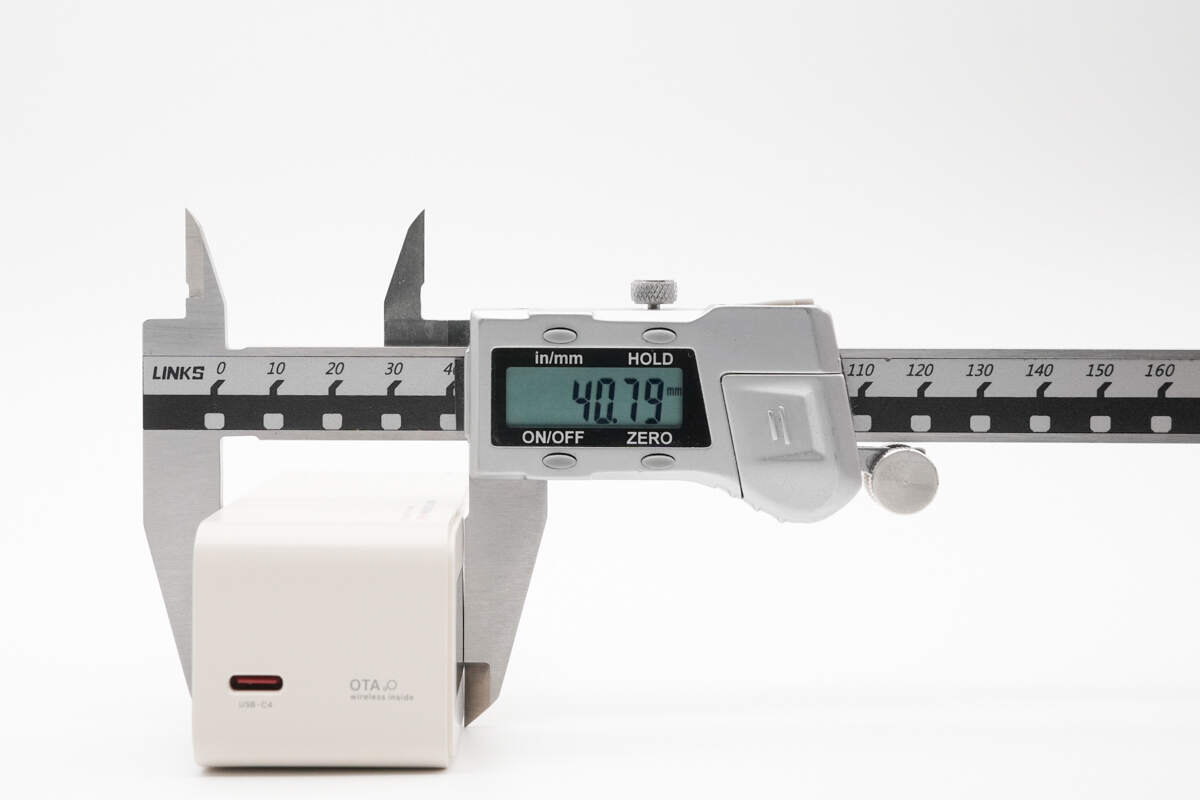
The length of the charger module is about 40.79 mm (1.61 inches).
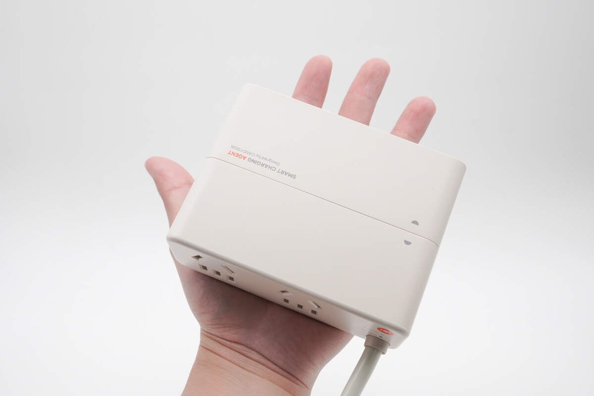
That's how big it is in the hand.
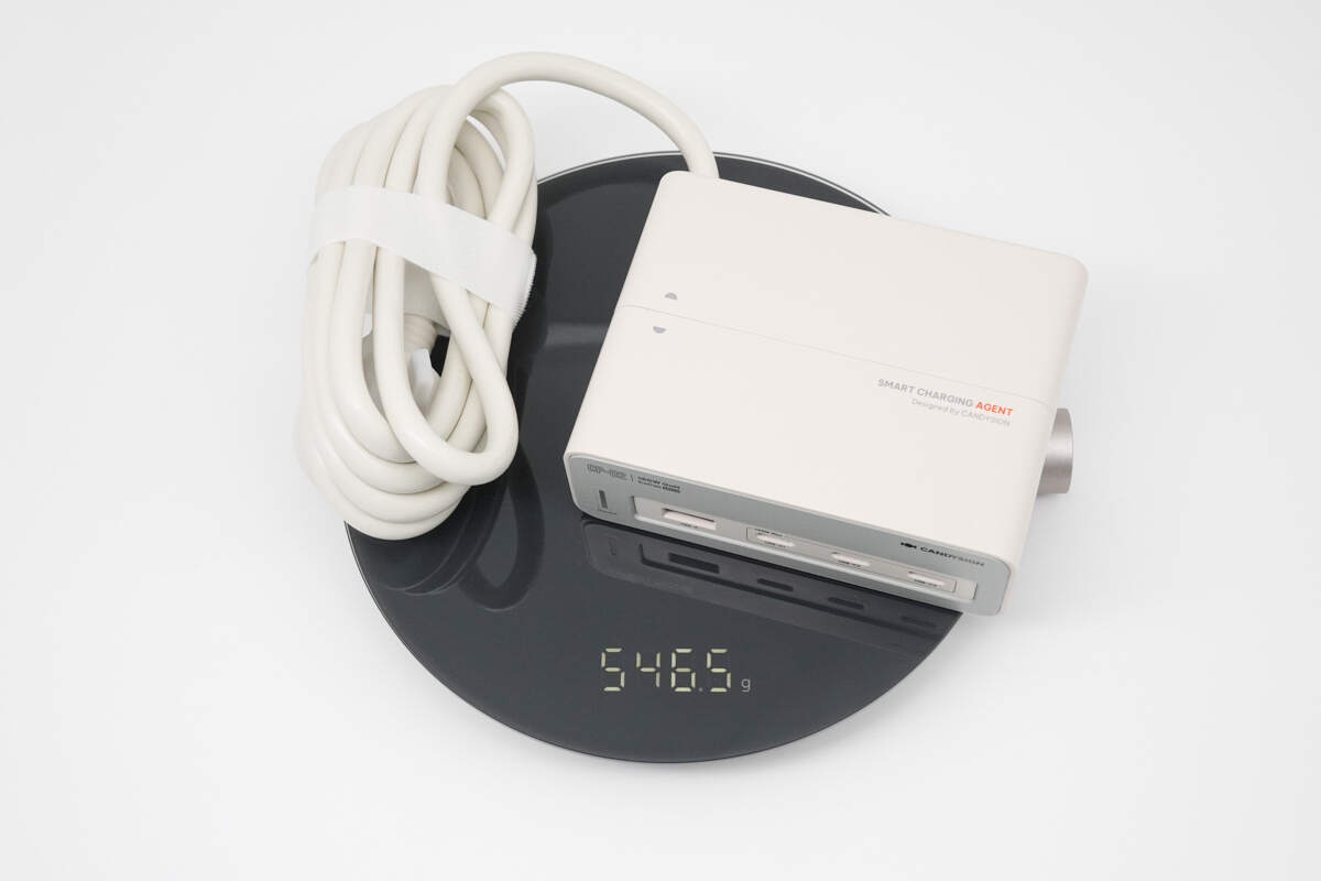
The total weight is about 547 g (19.29 oz).
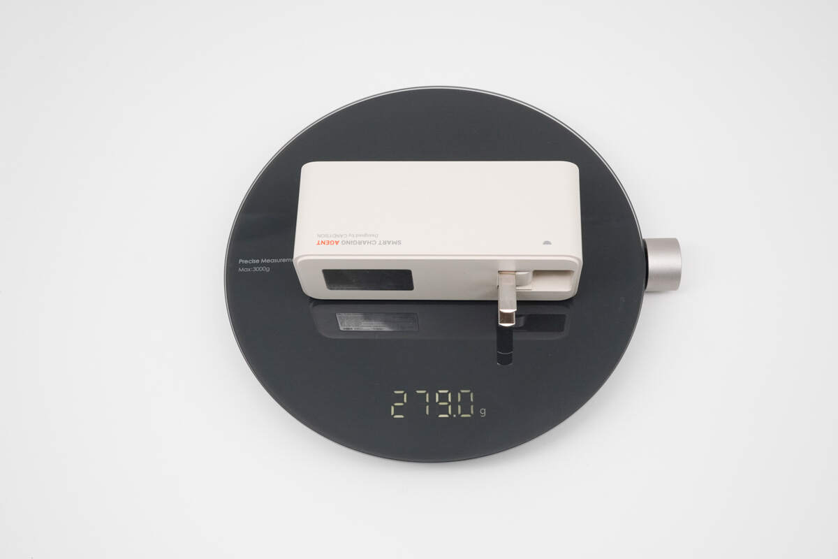
The weight of the charger module is about 279 g (9.84 oz).
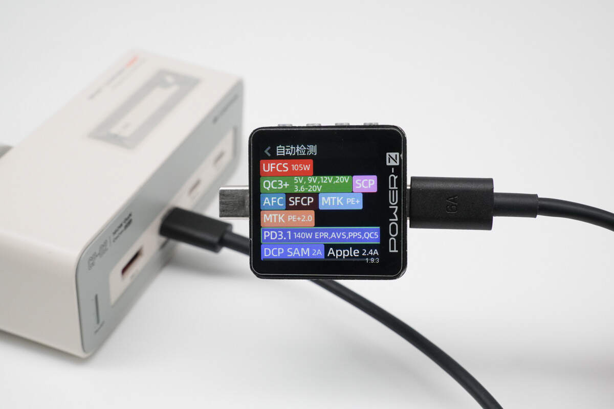
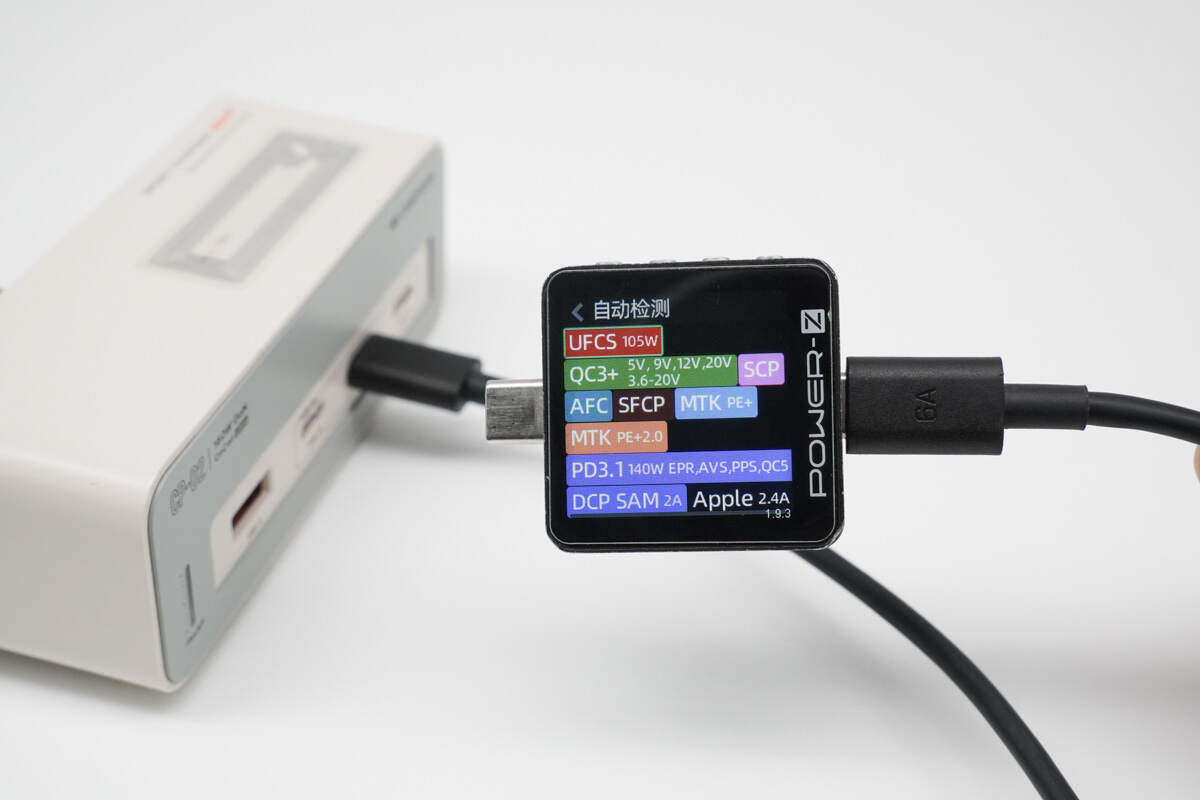
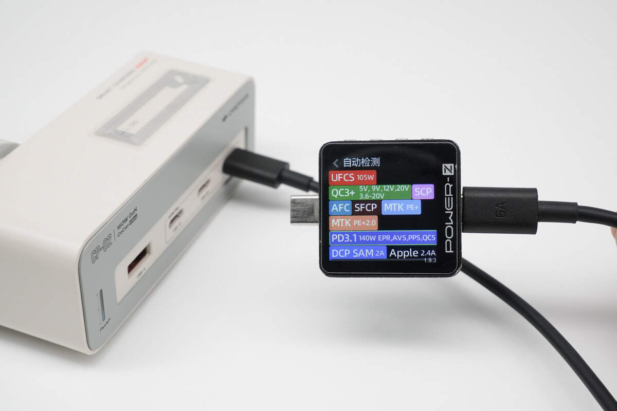
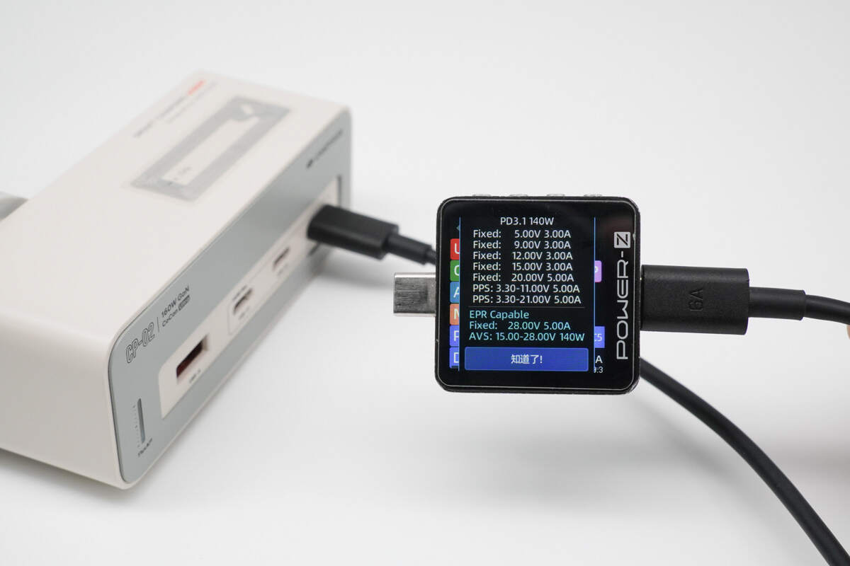
ChargerLAB POWER-Z KM003C shows that the USB-C1 supports UFCS, QC3+/5, SCP, AFC, SFCP, PE2.0, PD3.1, PPS, DCP, SAM 2A, and Apple 2.4A charging protocols.
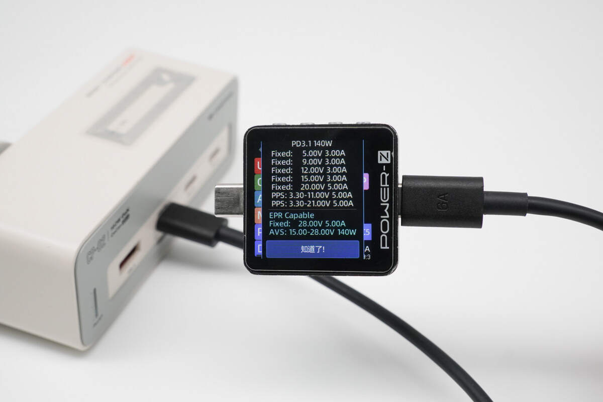
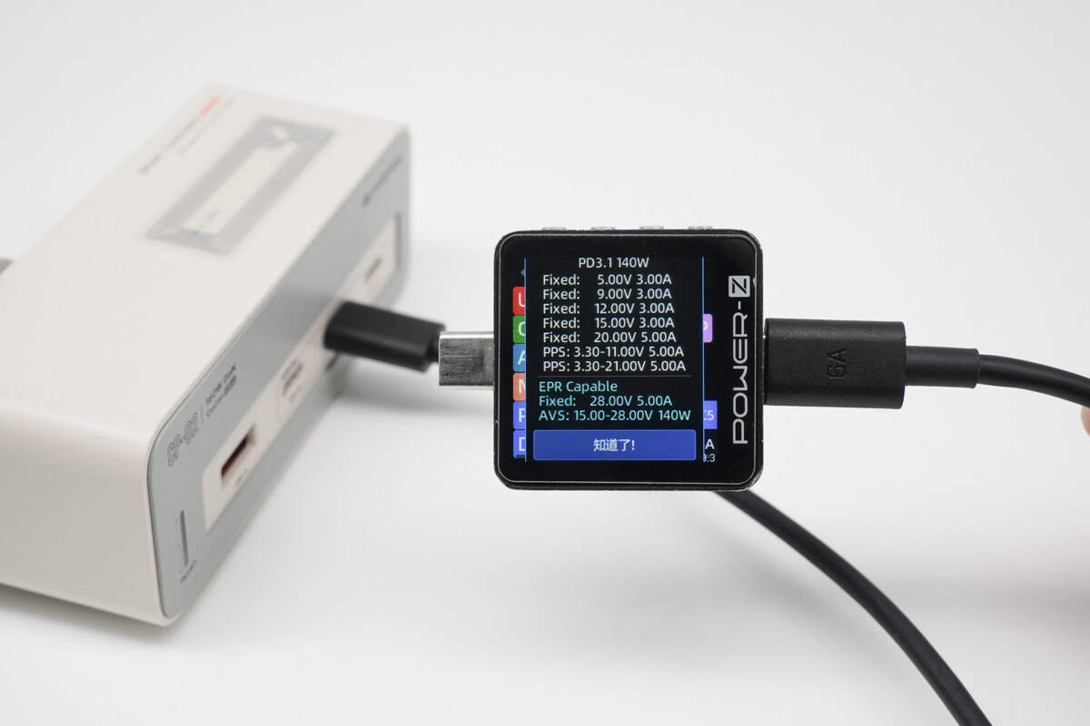
And it has six fixed PDOs of 5V3A, 9V3A, 12V3A, 15V3A, 20V5A, and 28V5A. It has two sets of PPS, which are 3.3-11V5A and 3.3-21V5A. It also has one set of AVS, which is 15-28V 140W.
The USB-C2 port supports the same protocols as the USB-C1 port.
The PDO profiles are also identical between the USB-C2 and USB-C1 ports.
The USB-C3 port supports the same protocols as the first two ports.
The PDO profiles for the USB-C3 port are also the same as those for the first two ports.
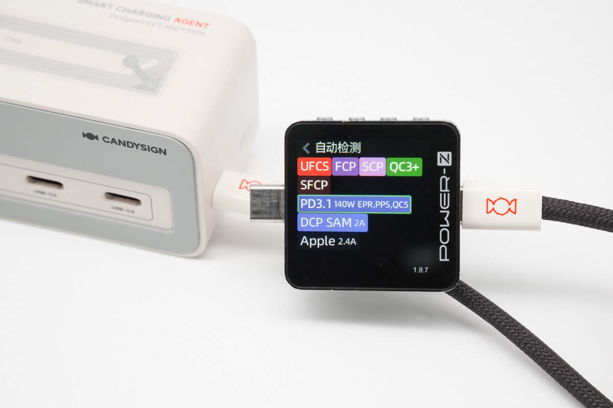
ChargerLAB POWER-Z KM003C shows that the USB-C4 supports UFCS, FCP, SCP, QC3+/5, SFCP, PD3.1, PPS, DCP, SAM 2A, and Apple 2.4A charging protocols.
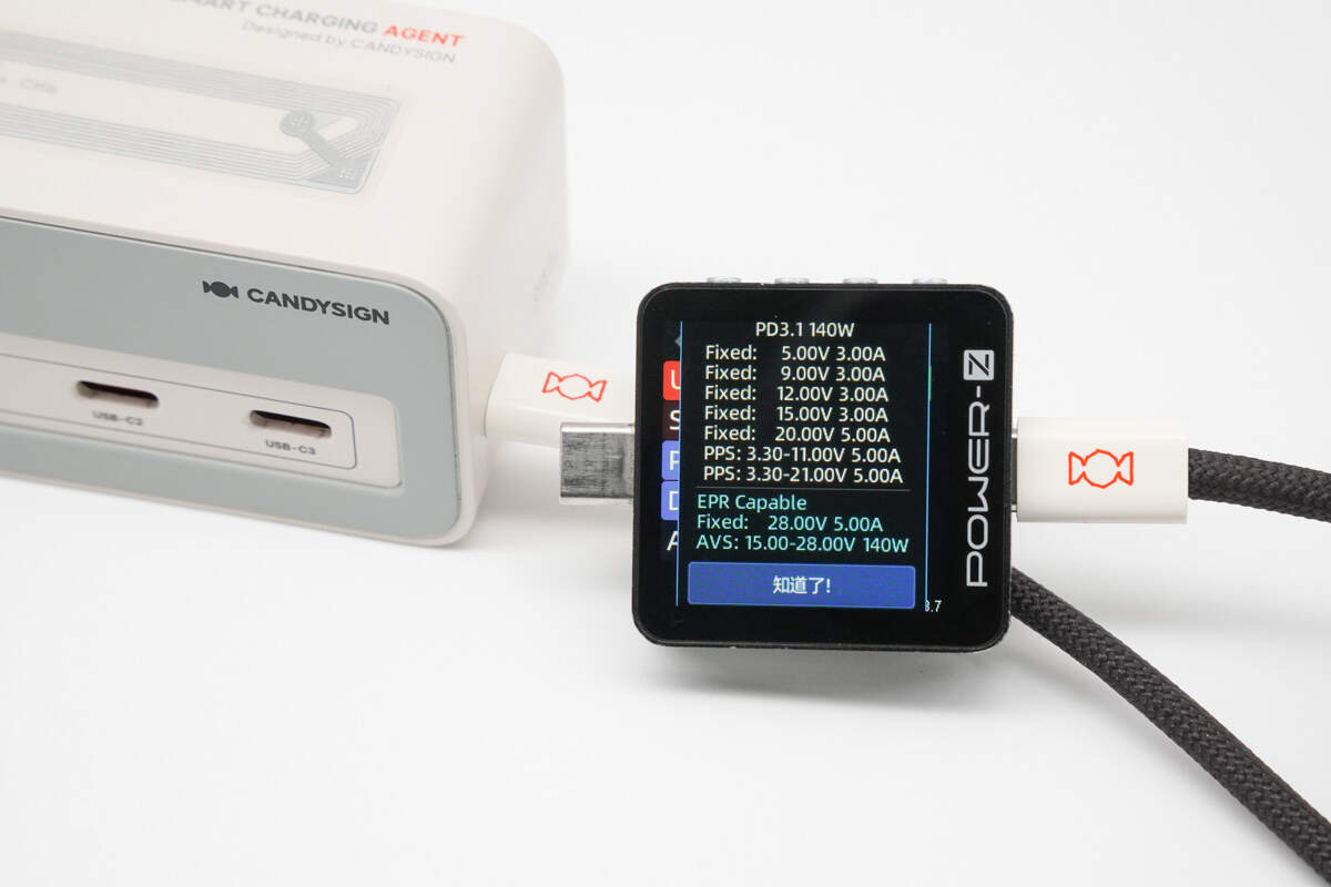
The PDO profiles are also the same.
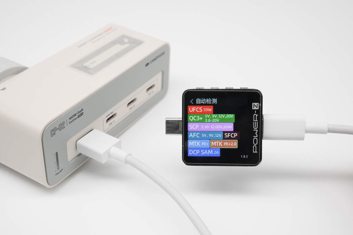
ChargerLAB POWER-Z KM003C shows that the USB-A supports UFCS, QC3+, SCP, AFC, SFCP, PE2.0, DCP, and SAM 2A charging protocols.
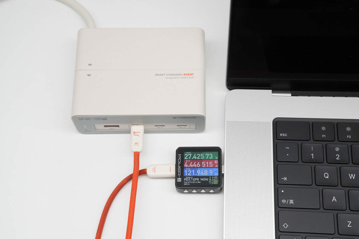
Charging a MacBook Pro 16 M4 Pro via the USB-C1 port measured a power output of about 121.95W, successfully enabling PD 3.1 fast charging.
Teardown
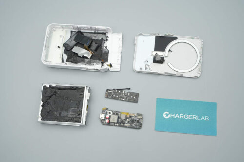
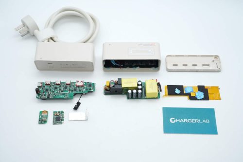
Next, let's take it apart to see its internal components and structure.
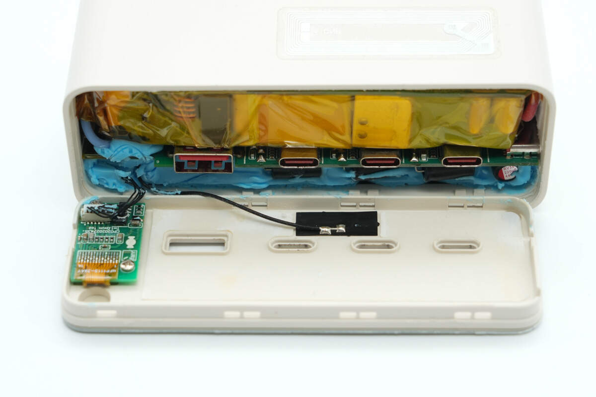
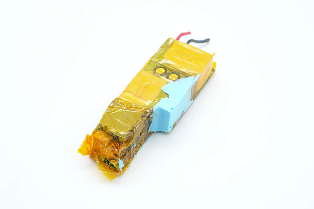
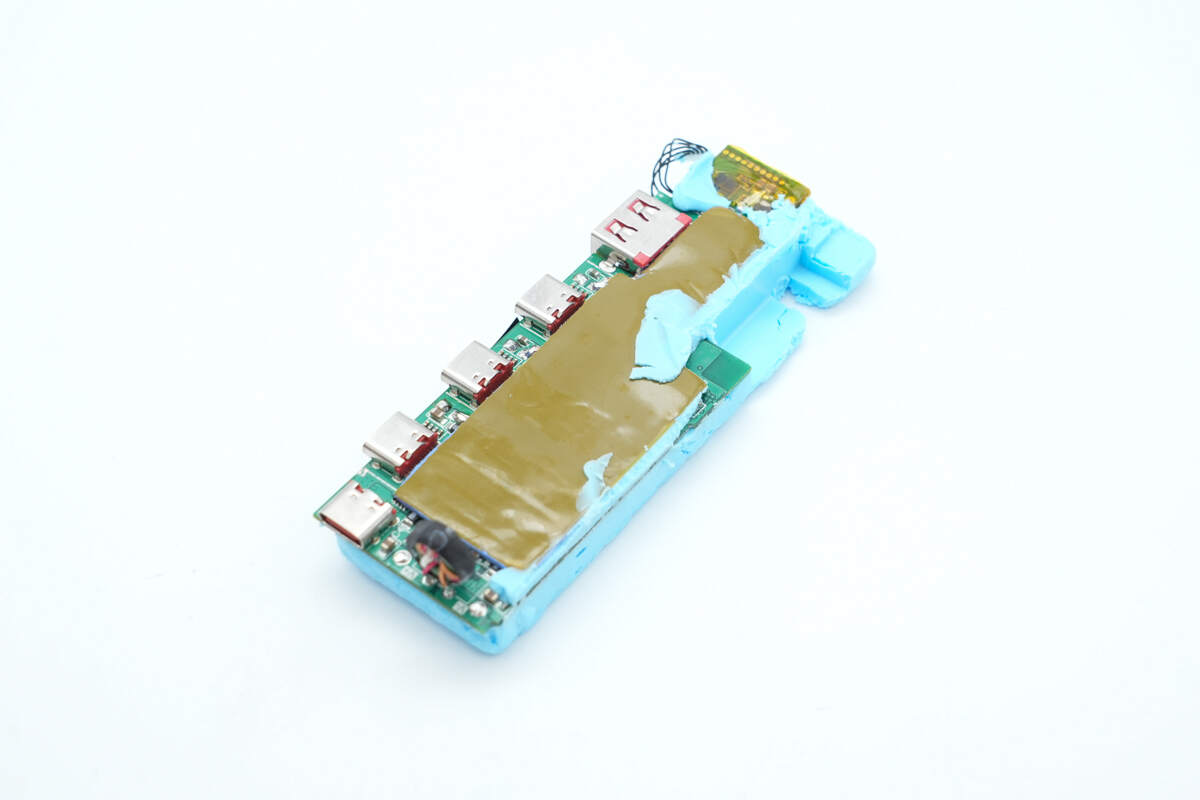
The casing can be opened along the seam, revealing the power module wrapped in high-temperature tape, with blue thermal gel filling the gap between the module and the housing.
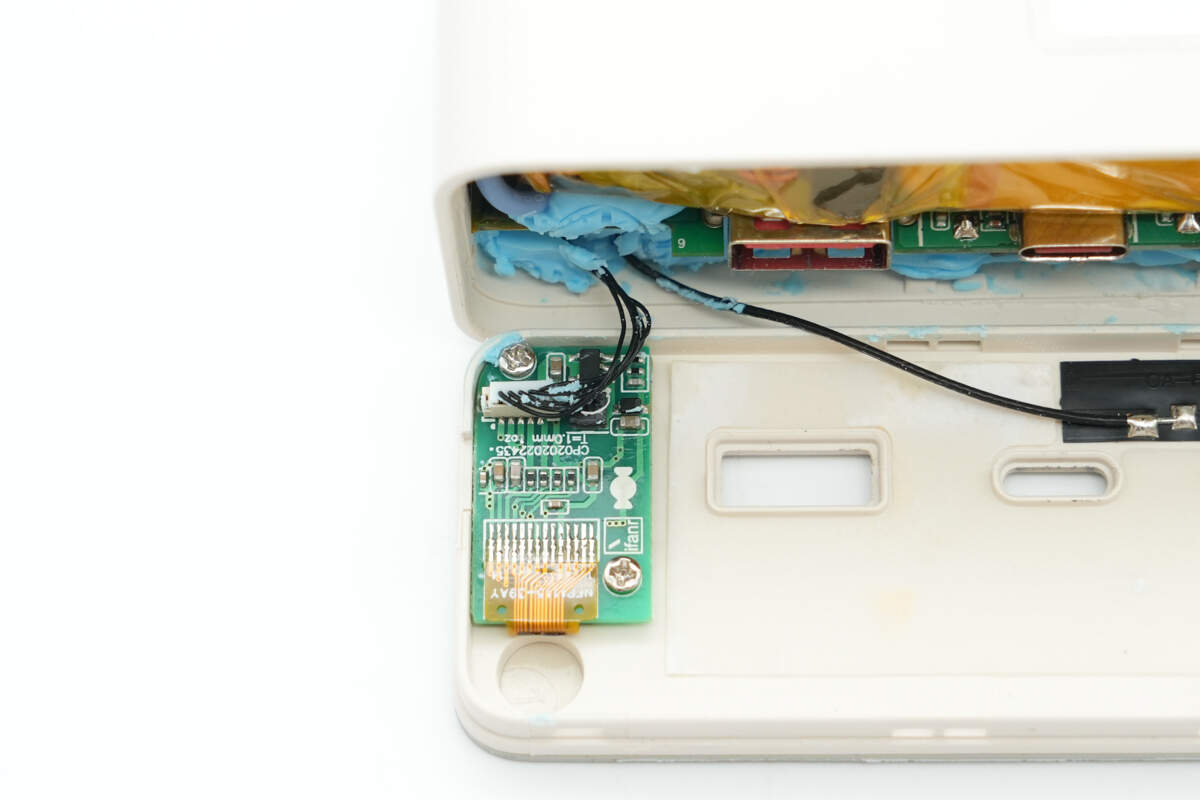
The OLED infinite light column PCB is connected via wiring.

The FPC antenna is used for wireless communication.
The PCBA module is secured in place with clips.
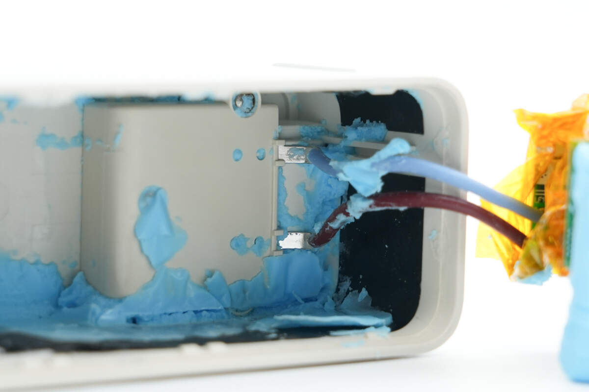
The PCBA module is connected to the prongs via wiring.
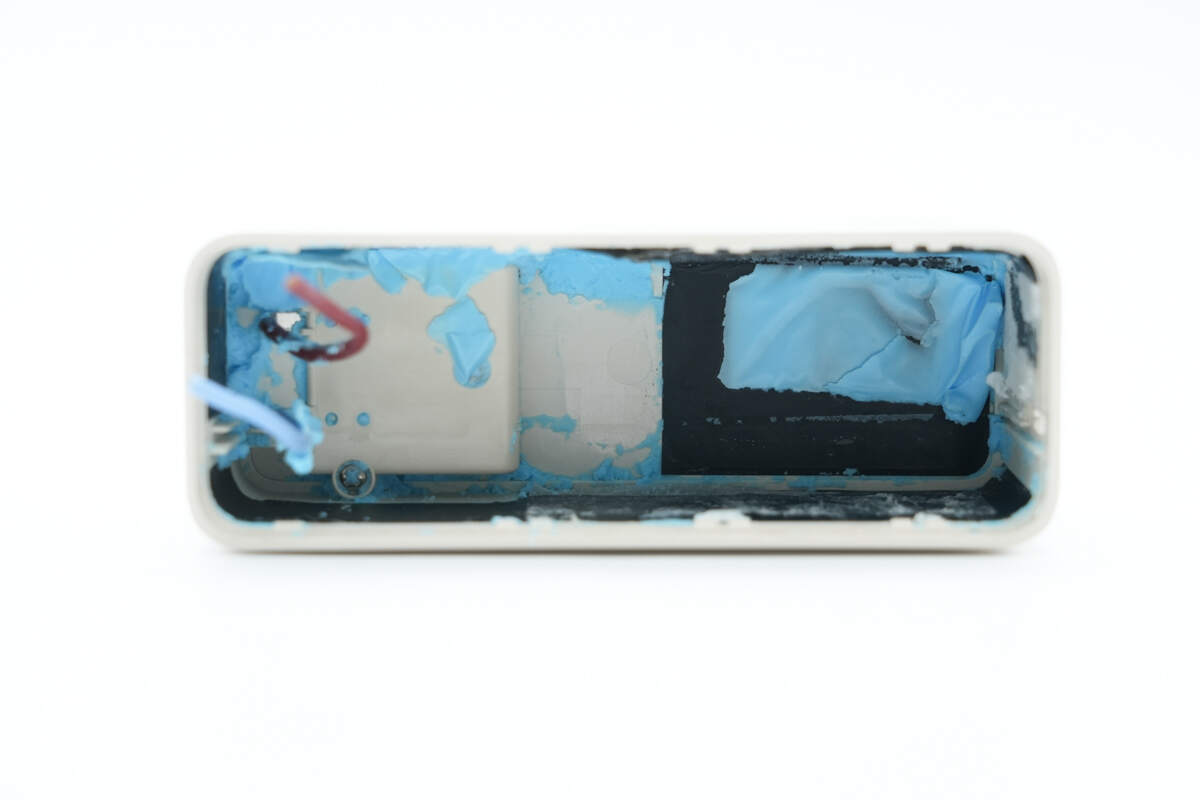
Graphite thermal pads are applied inside the housing to enhance heat dissipation.
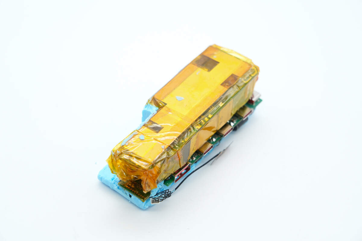
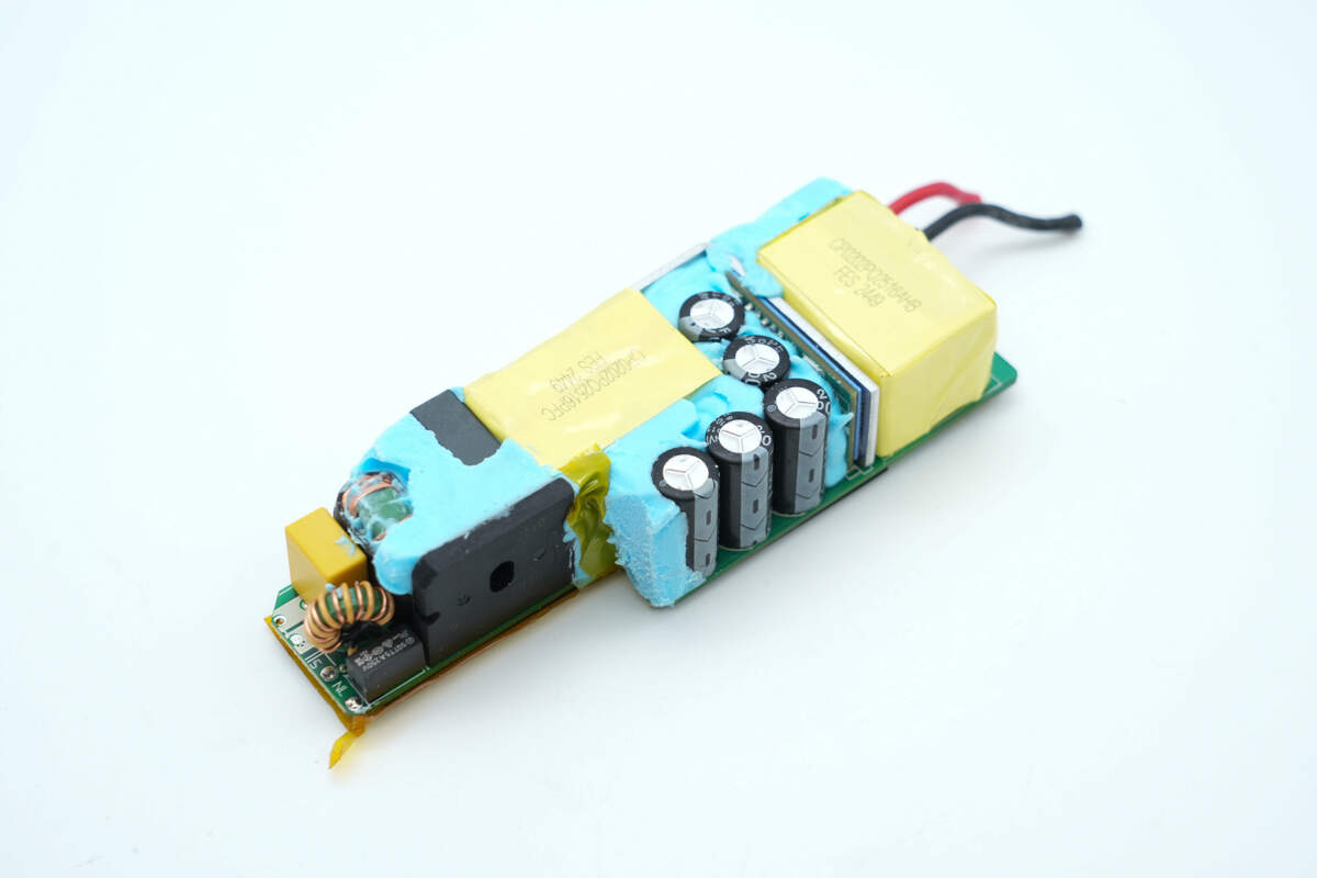
The entire PCBA module is wrapped with high-temperature tape.
The other side is coated with blue thermal gel.
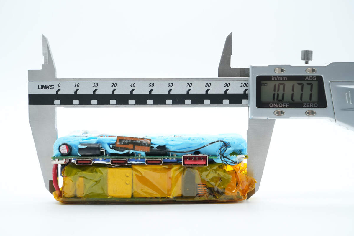
The length of the PCBA module is about 101.8 mm (4.0079 inches).
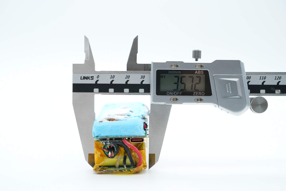
The width is about 35.7 mm (1.41 inches).
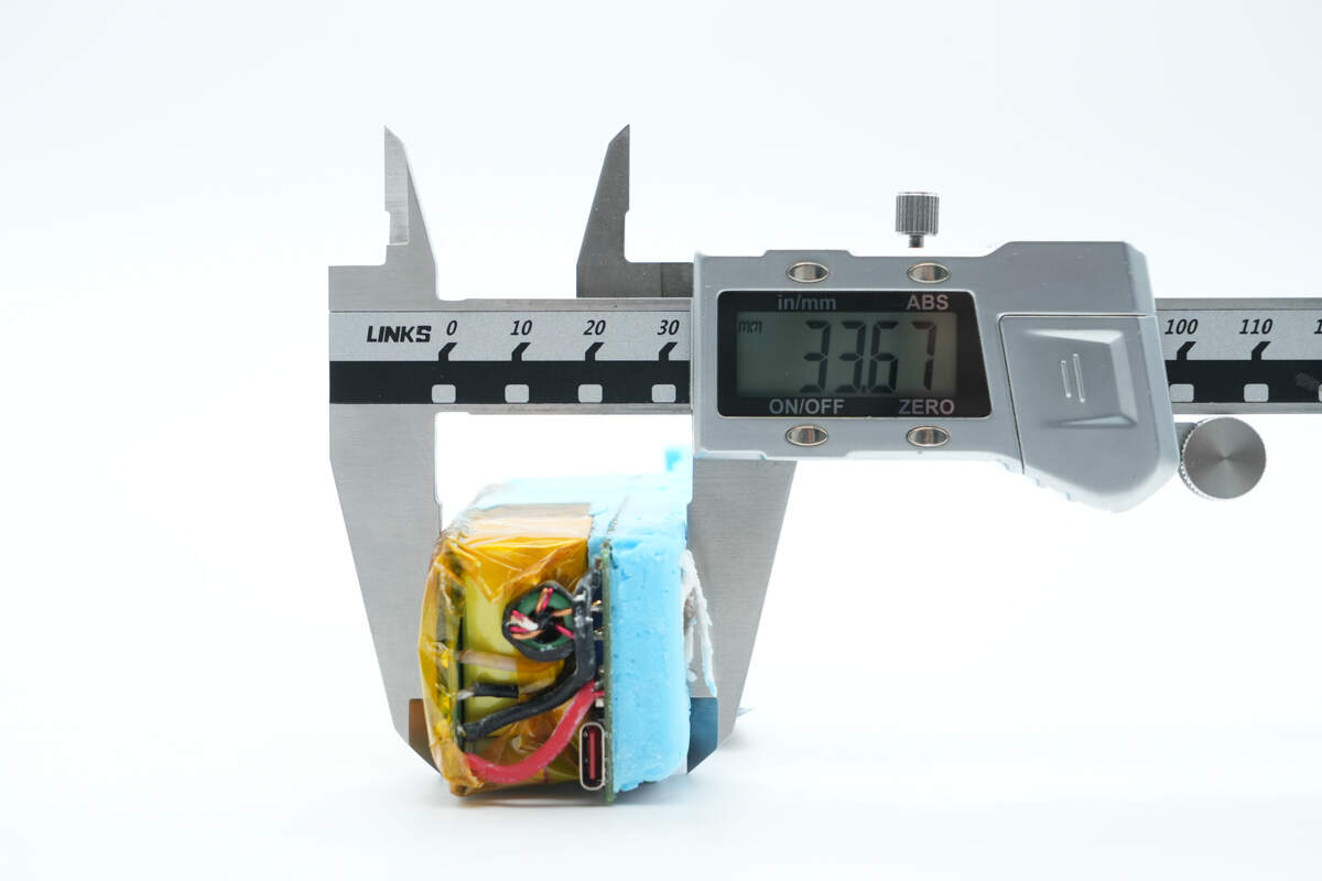
The thickness is about 33.7 mm (1.33 inches).
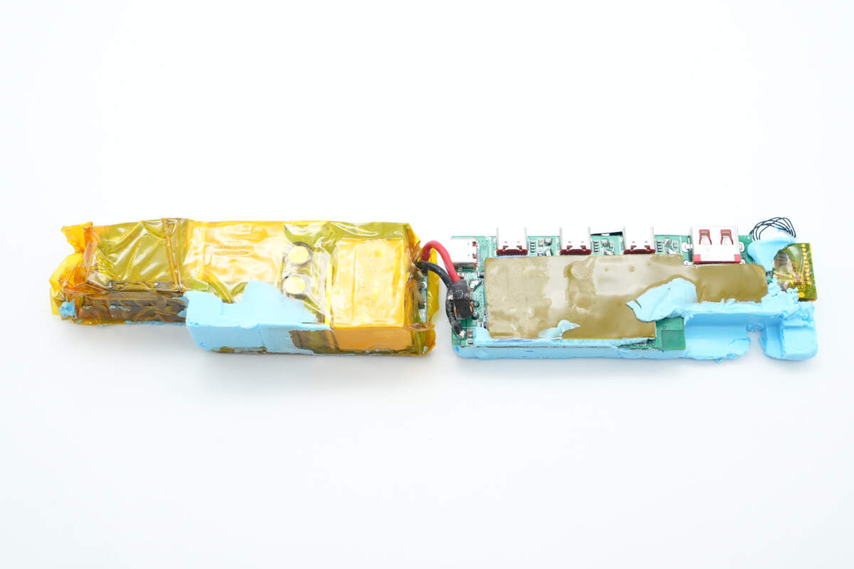
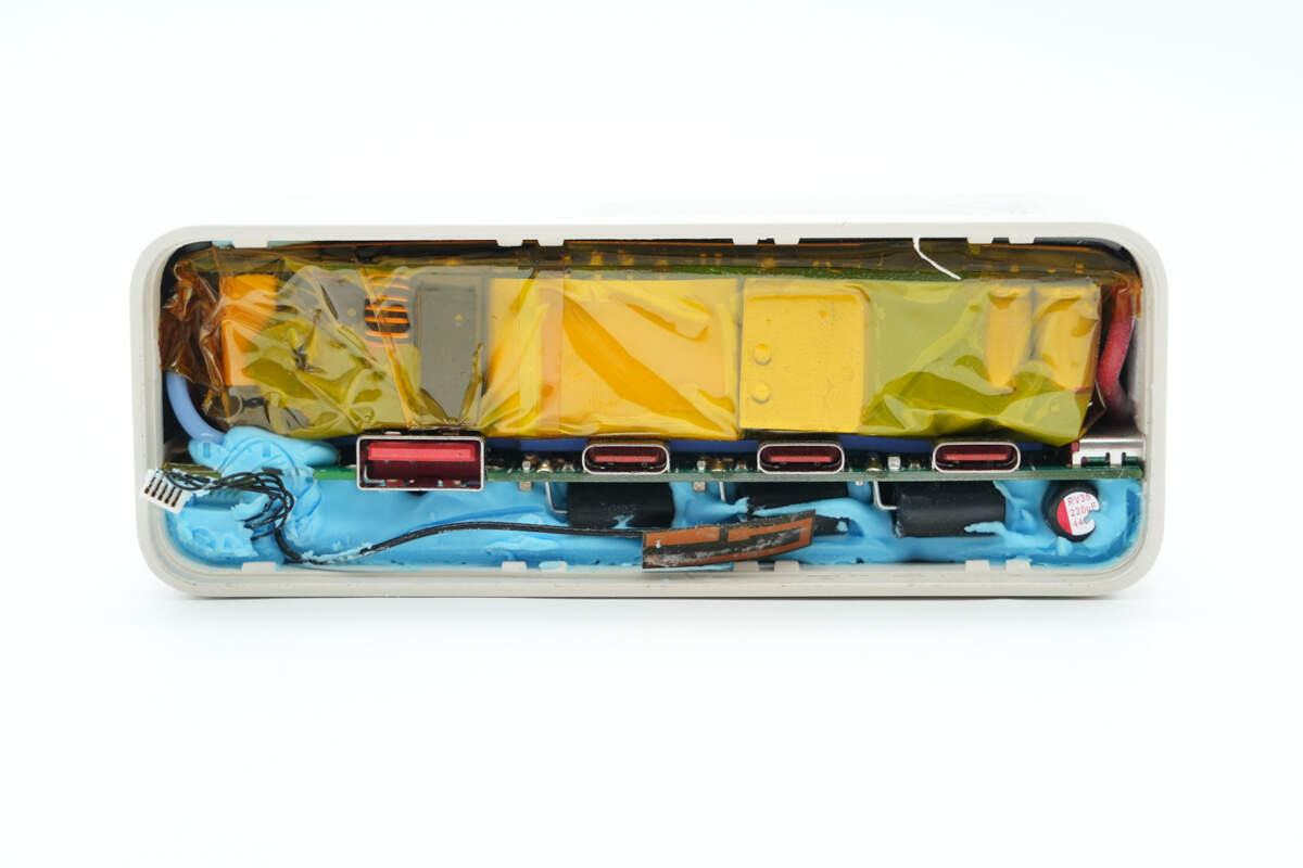
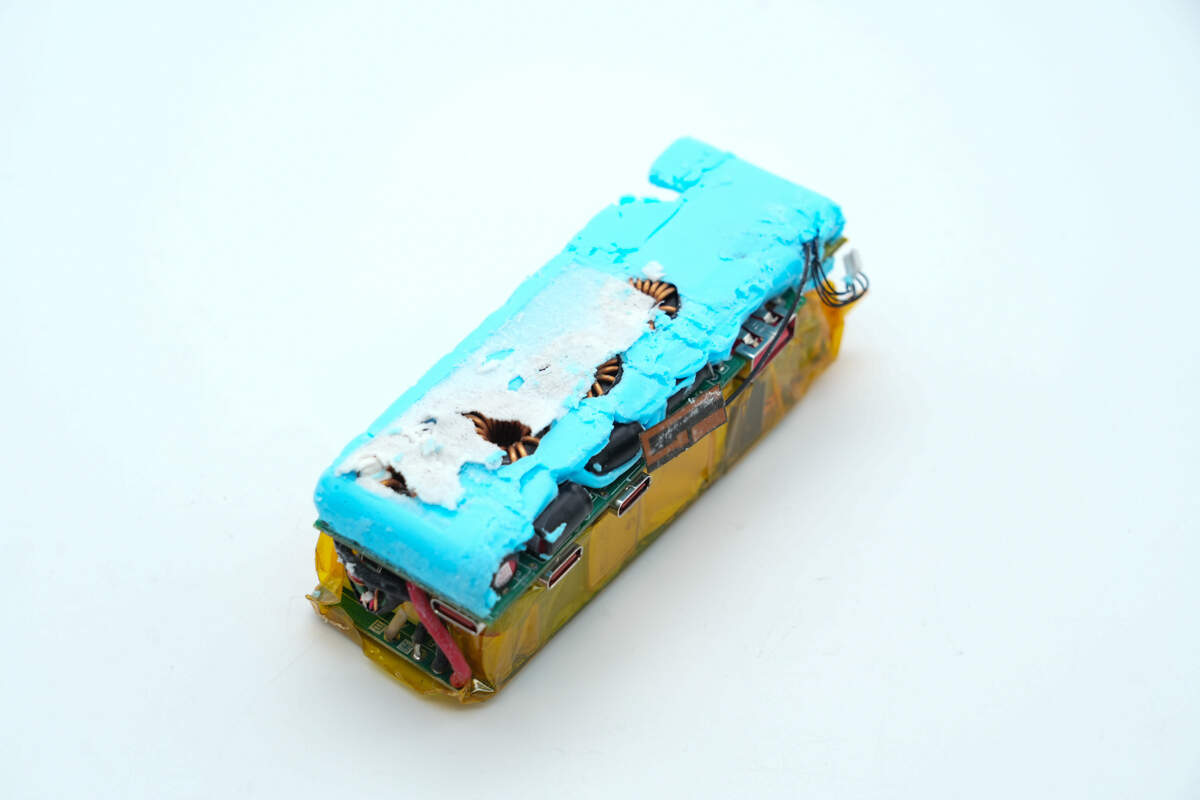
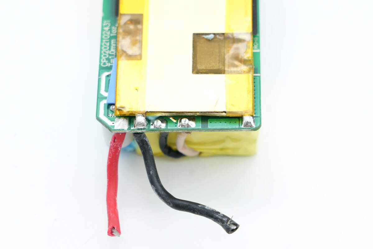
The power PCB and the buck converter PCB are separated, connected by wiring.
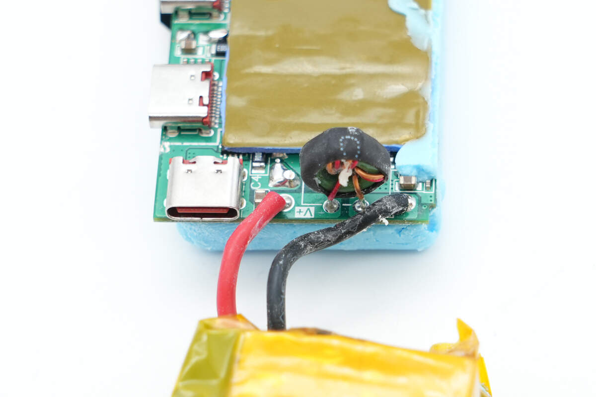
The wires are soldered to the buck converter PCB to supply power.
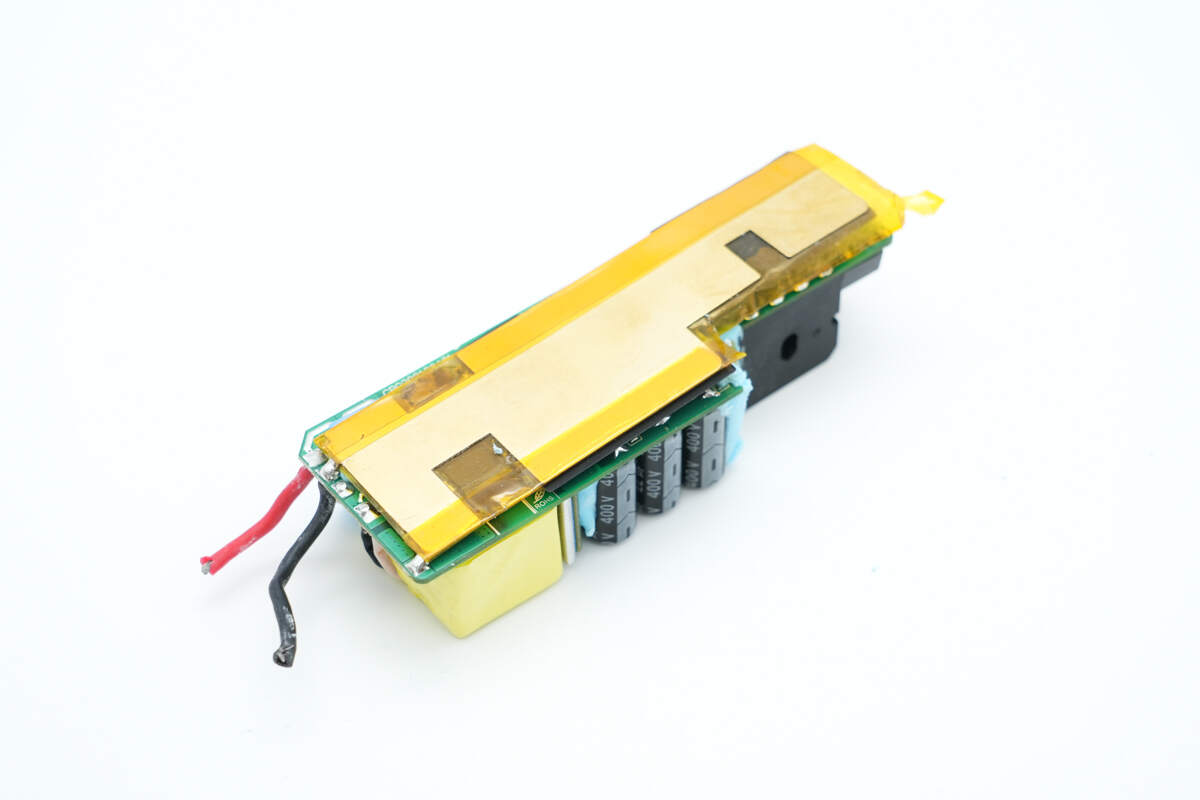
The power PCB is fully wrapped in high-temperature tape for insulation.
After removing the tape, the gaps around components such as capacitors and the transformer are also filled with thermal gel.
The back side features a copper plate for heat dissipation.
The copper plate is secured by soldering.
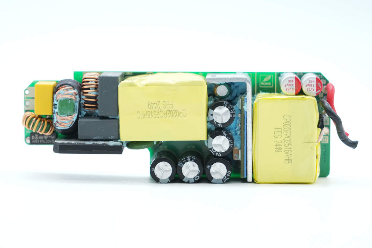
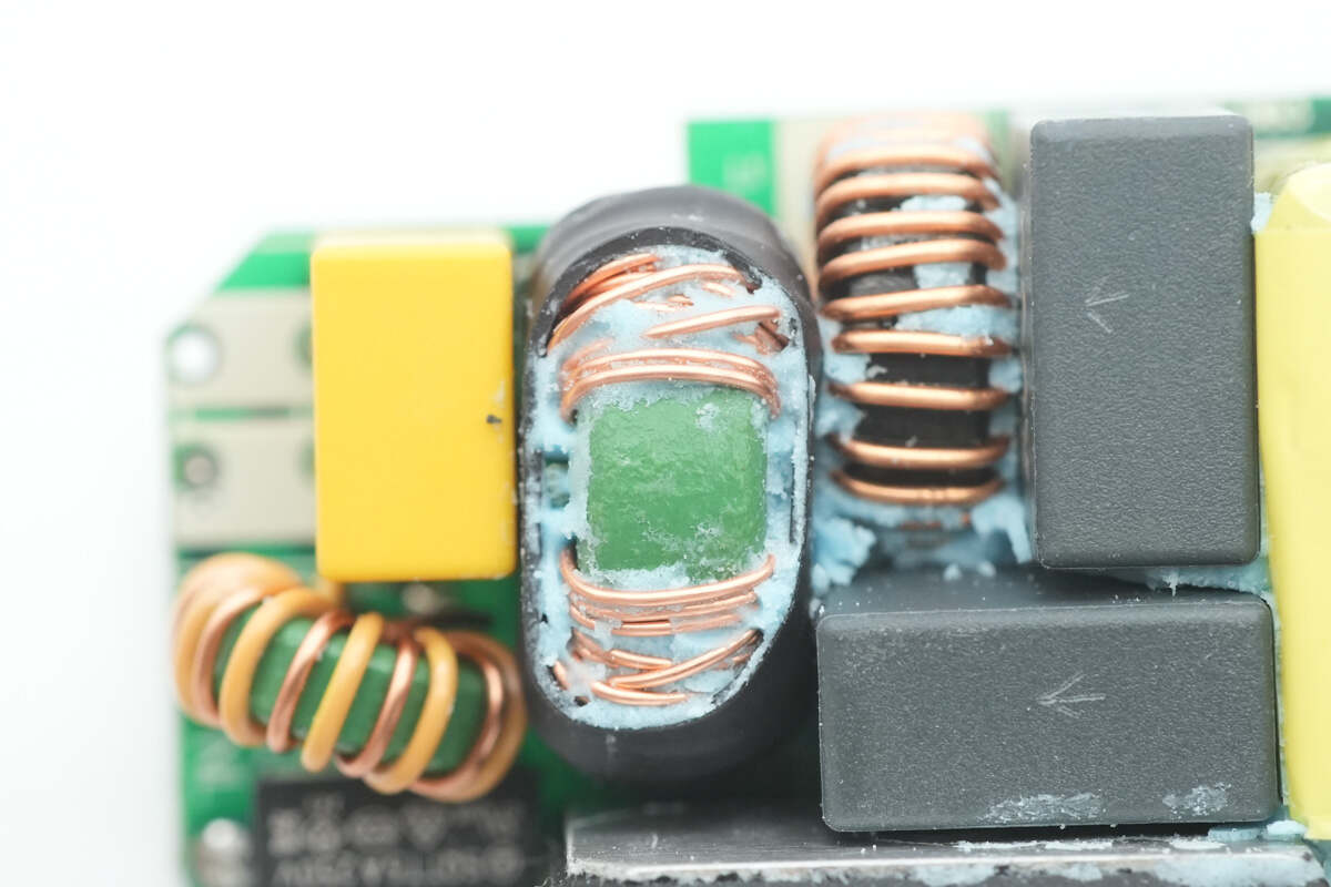
After removing the thermal gel, the left side reveals the input end, which includes a fuse, common mode chokes, a safety X2 capacitor, a bridge rectifier, filtering capacitors, and filter inductors. In the center is the PFC boost inductor.
To the right and below the PFC boost inductor are high-voltage filtering capacitors. On the right side, there's a small PCB attached to a heatsink via a thermal pad for heat dissipation. Also on the right are the transformer and solid capacitors.
On the back side, there are the PFC controller, GaN FET, and silicon carbide diode. On the left side are the feedback optocoupler, SMD Y-capacitors, and synchronous rectifiers.
The input end includes a fuse, common mode chokes, and a safety X2 capacitor.
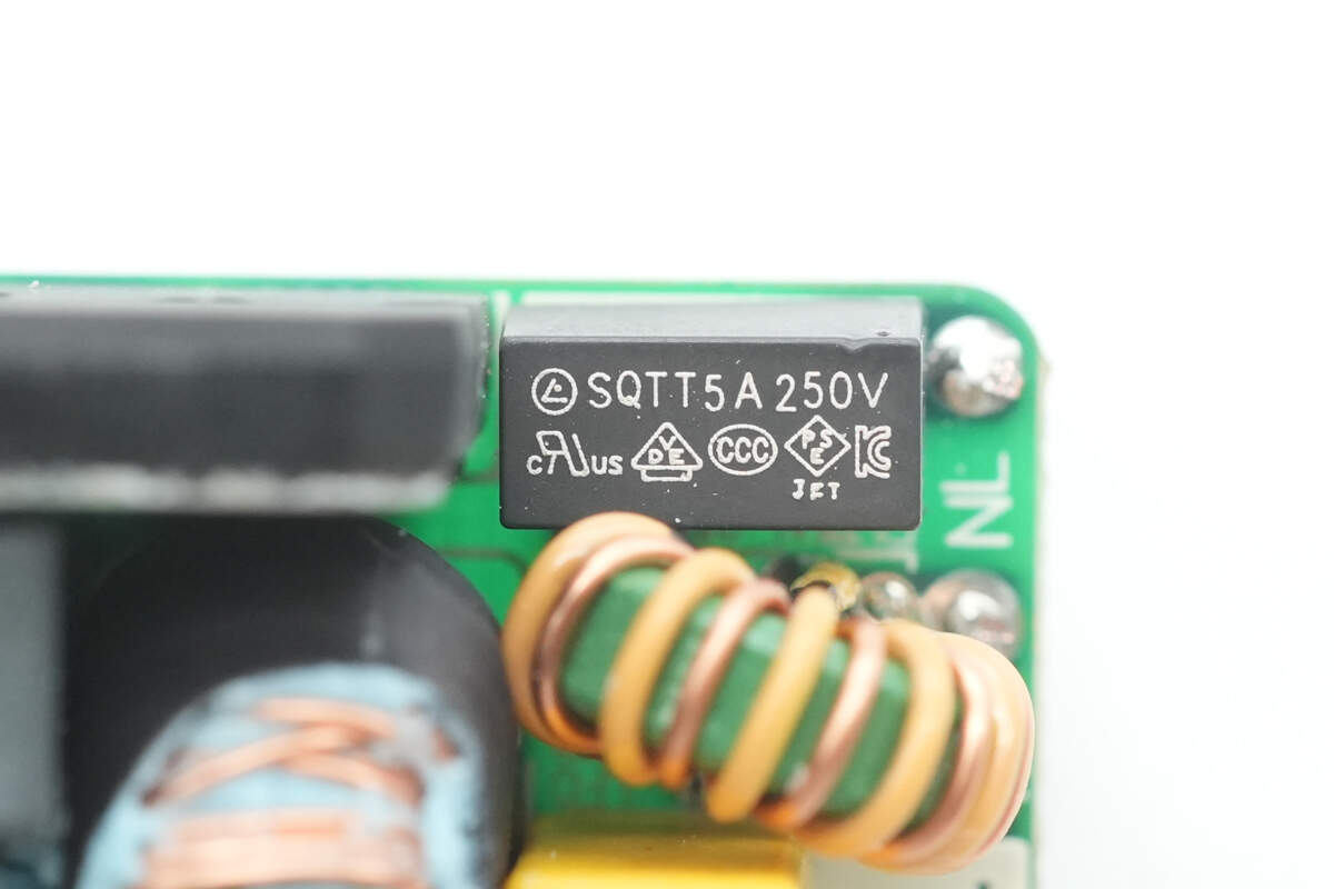
The input fuse is rated at 5A 250V.
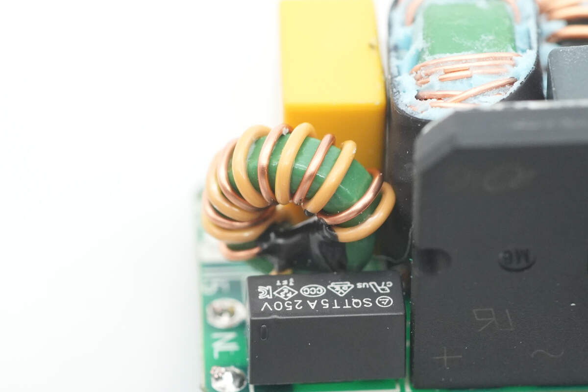
The common mode choke is wound with both enameled wire and insulated wire.
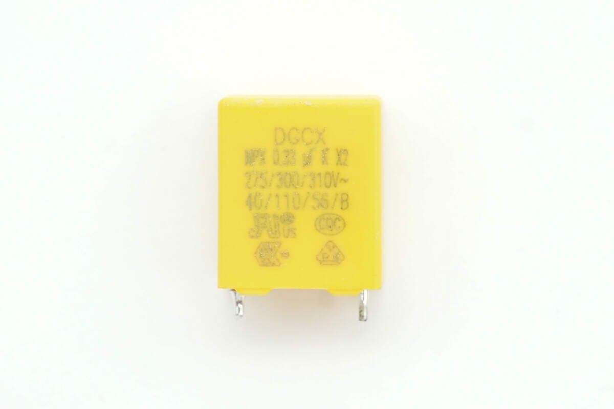
The safety X2 capacitor is manufactured by DGCX and is rated at 0.33μF.
The other common mode choke is wound with enameled wire and insulated with heat shrink tubing.
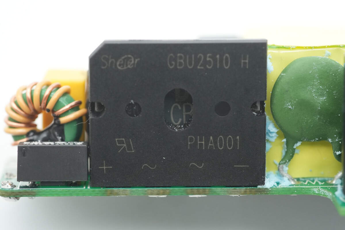
The bridge rectifier is manufactured by Sheier, model GBU2510 H. It is rated for 1000V and 25A, and comes in a GBU package.
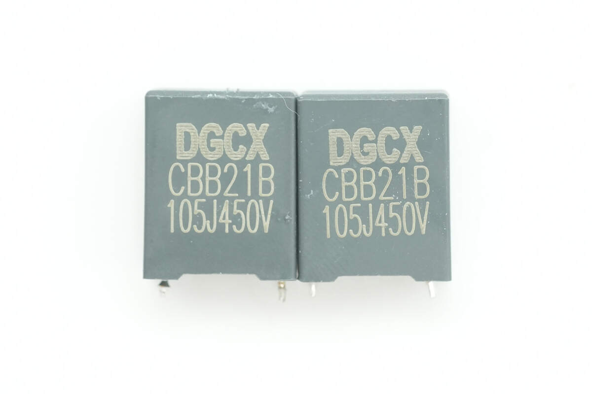
The film capacitors are manufactured by DGCX and are rated at 1μF 450V.
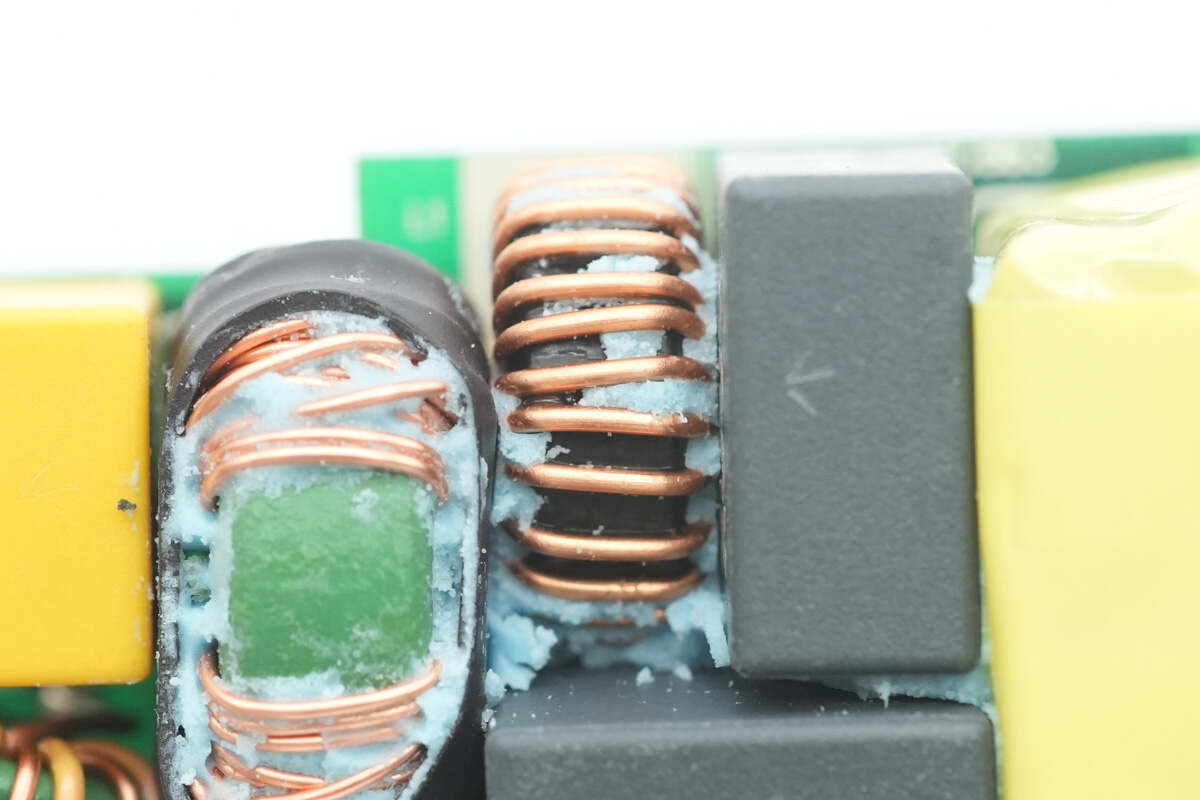
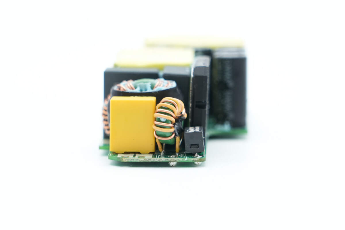
The filter inductor is wound around a ferrite core.
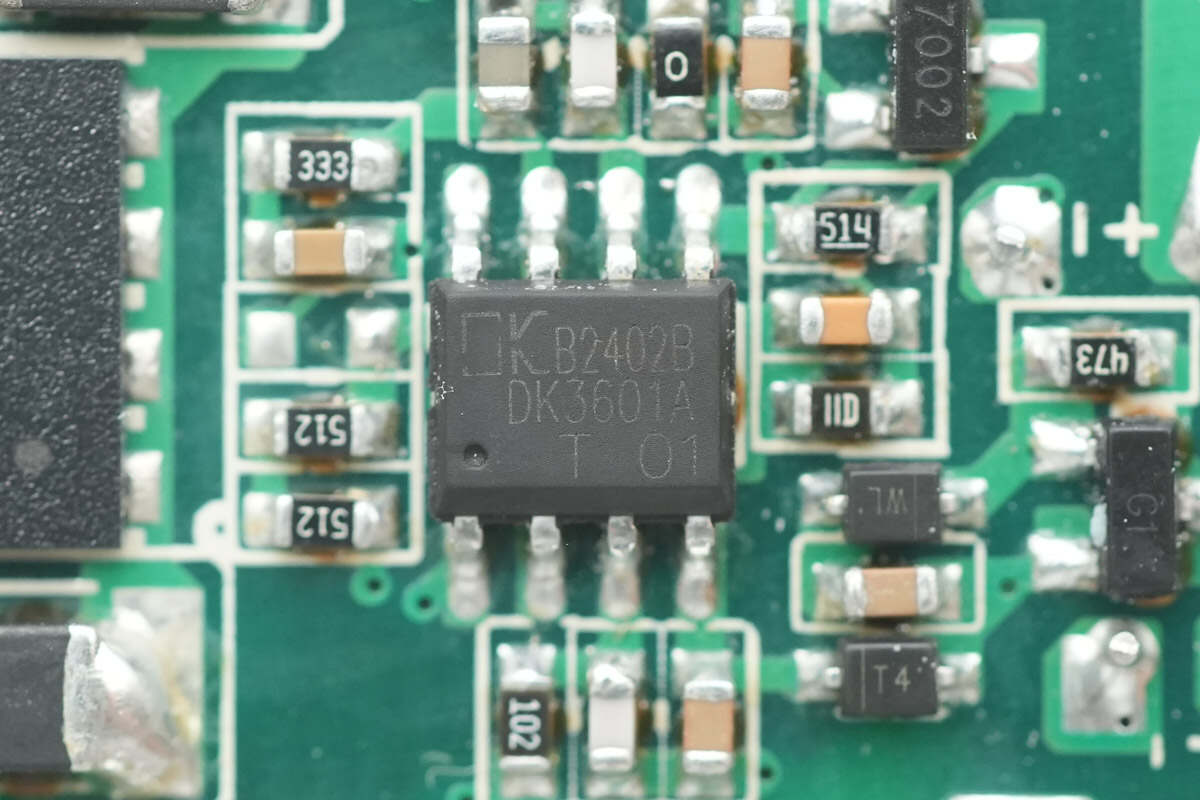
The PFC controller is manufactured by DONGKE, model DK3601A. It operates in critical conduction mode (CRM) and features output overvoltage and overcurrent protection. It also has a built-in X-capacitor discharge function and comes in an SOP-8 package.
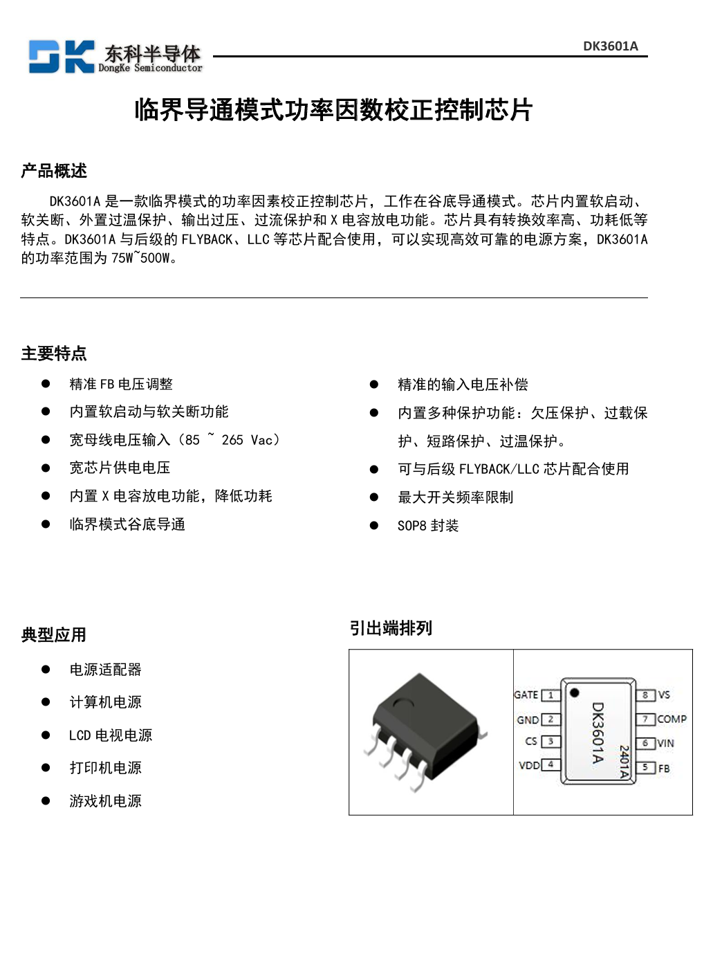
Here is the information about DONGKE DK3601A.
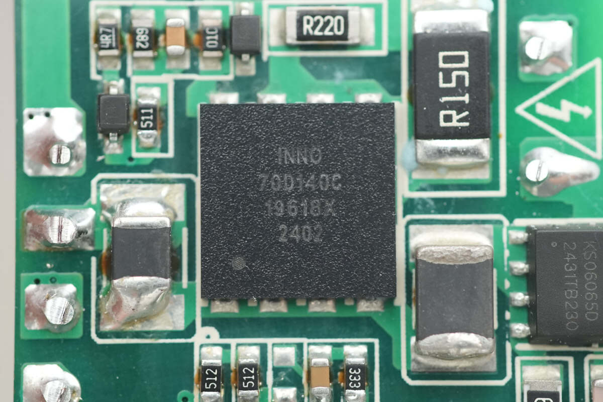
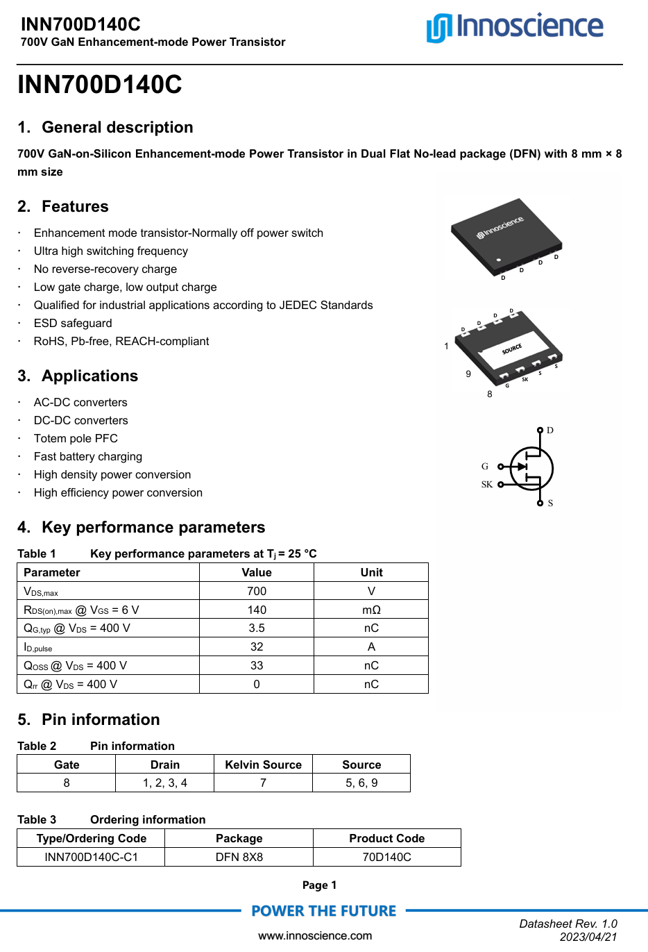
The PFC MOSFET is manufactured by Innoscience, marked with 70D140C, model INN700D140C. It is an enhancement-mode GaN FET rated for 700V, with a transient voltage withstand of 800V, an RDS(on) of 140mΩ, and features a Kelvin source pin. It comes in a DFN 8×8 package.
Innoscience’s GaN FETs offer ultra-low gate charge and output charge, meeting JEDEC industrial application standards, and include integrated ESD protection. They are RoHS-compliant, lead-free, and conform to EU REACH regulations. These devices are suitable for totem-pole PFC circuits, fast charging power supplies, high power density designs, and high-efficiency switching power supply applications.
Here is the information about Innoscience INN700D140C.

The shunt resistor is used to monitor the current of the PFC MOSFET. 150mΩ.
The PFC boost inductor is tightly wound and insulated with tape.
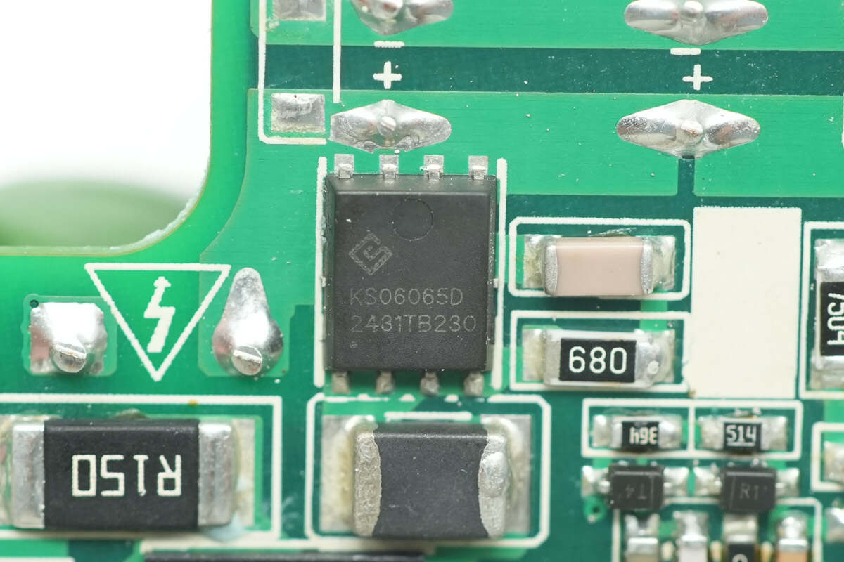
The PFC rectifier is from SGKS, model KS06065D. It is a silicon carbide (SiC) Schottky diode rated at 650V and 6A, packaged in a PDFN 5×6 case.
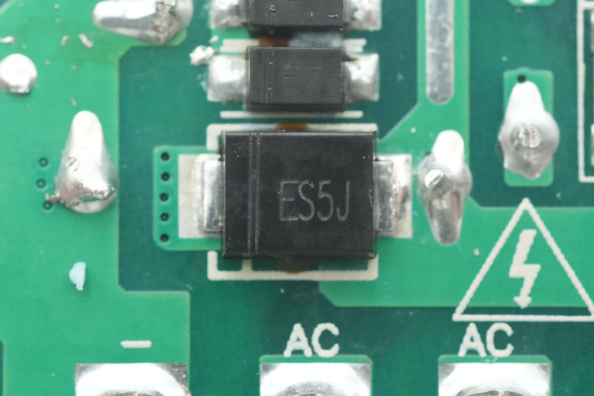
The ES5J fast recovery diode is used for PFC bypass.
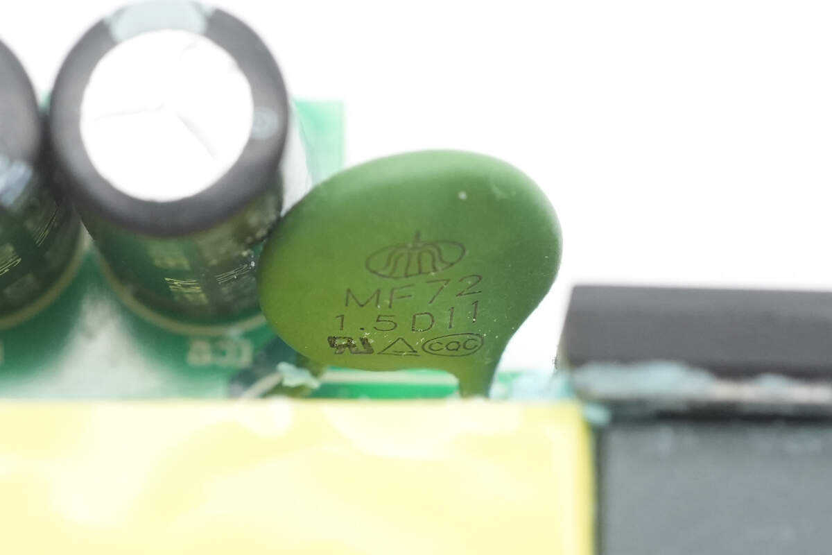
The NTC thermistor is from Shiheng, part of the MF72 series, marked with 1.5D11. It is used to suppress inrush current during power-up.
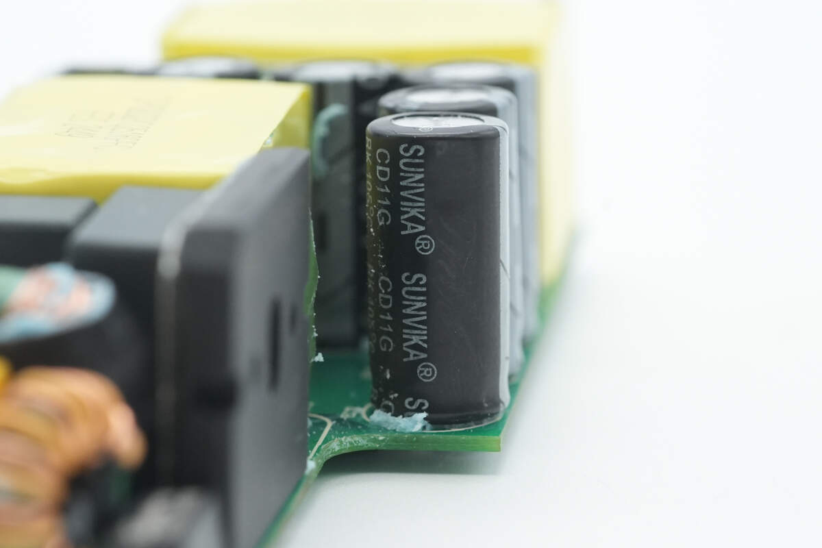
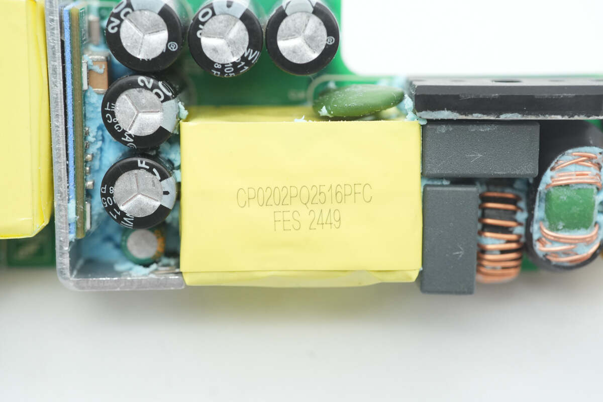
The high-voltage filter capacitors are sourced from SUNVIKA.
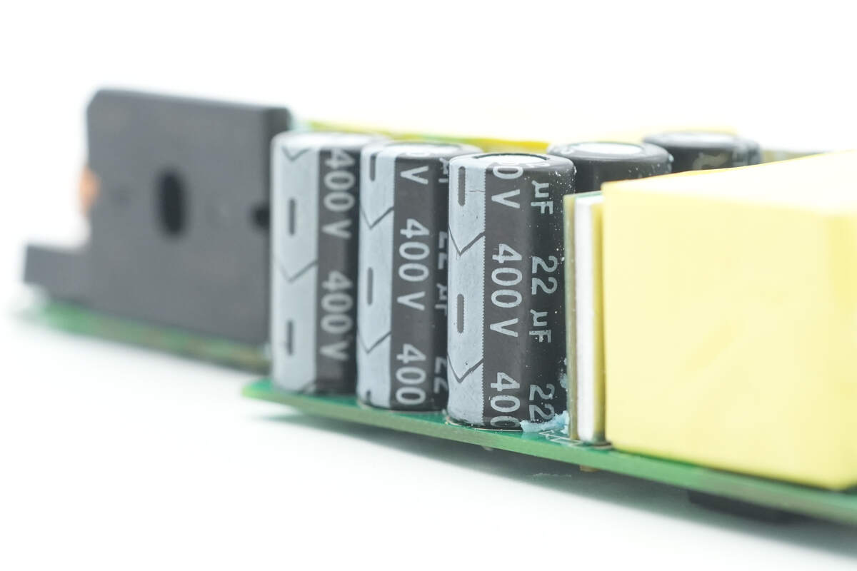
The filter capacitors are rated at 22μF 400V each, with five units connected in parallel for a total capacitance of 110μF.
The AHB GaN chip is soldered onto the vertical PCB, with current-sense resistors on the left side and resonant capacitors on the right side.
The back side dissipates heat through a thermal pad.
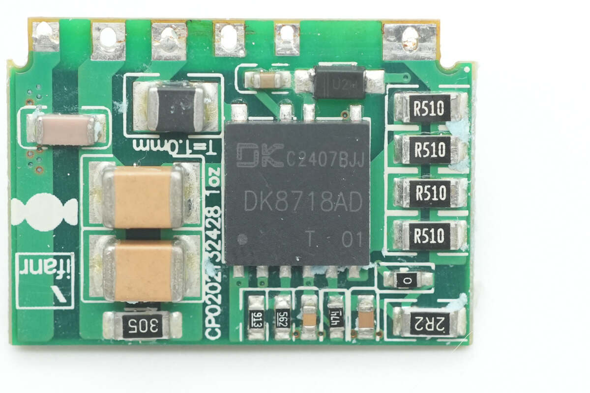
The AHB GaN chip is from DONGKE, model DK8718AD. It is an AC-DC power switching chip based on an asymmetric half-bridge architecture, integrating two GaN power devices. It achieves ZVS on the primary power transistor and ZCS on the secondary rectifier over a wide load range, thereby improving power supply system efficiency. The soft switching also reduces stress on the power devices. It features a built-in full-range frequency dithering circuit, which reduces switching losses and improves EMI.
The DK8718AD supports a maximum switching frequency of 800kHz and is recommended for power supplies up to 180W when used with a front-end boost PFC. Its standby power consumption is less than 50mW. It includes adaptive dead-time and shutdown algorithms, eliminating the need for external tuning and allowing for minimal external components. The chip is halogen-free and RoHS compliant, with built-in high-voltage startup and X-capacitor discharge circuits, providing enhanced performance and reliability.
DK8718AD adapts to four different load modes to effectively improve efficiency across various load conditions. With the integration of the DK8718AD, conversion efficiency can reach up to 95.4%.
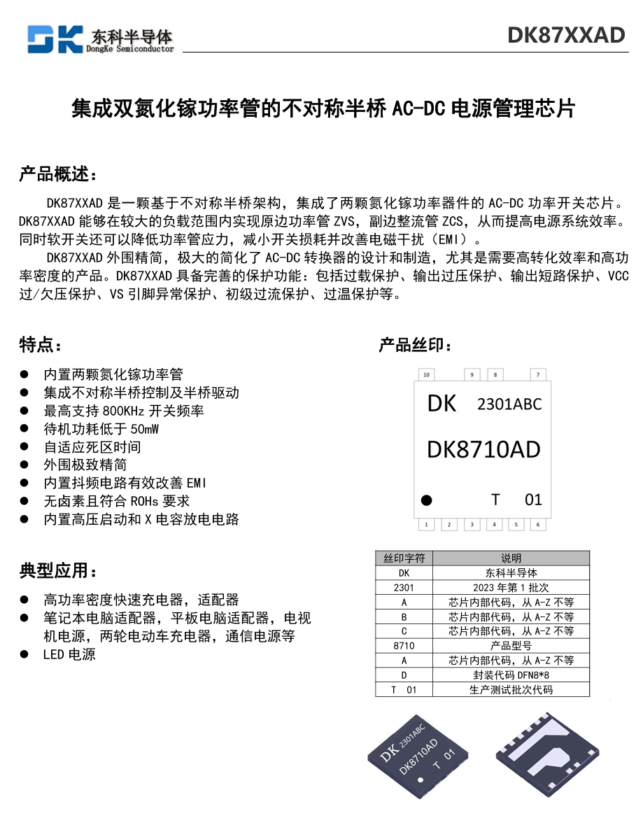
The DK8718AD integrates two 650V enhancement-mode GaN HEMTs, along with built-in half-bridge driver and asymmetric half-bridge control circuits. The upper and lower transistors feature adaptive dead-time and shutdown algorithms: the lower transistor adjusts dead-time adaptively, while the upper transistor adapts its shutdown timing. This eliminates the need for external tuning, greatly simplifying design and debugging.
The chip includes multifunction pins that support demagnetization detection, OVP, brown-in/brown-out detection, and more. It also has a negative CS sampling feature to enhance driving stability.
With a highly simplified external component requirement, the DK8718AD significantly streamlines the design and manufacturing of AC-DC converters, especially for products demanding high efficiency and high power density. It offers comprehensive protection features, including overload protection, output overvoltage protection, output short-circuit protection, VCC over-/under-voltage protection, VS pin fault protection, primary overcurrent protection, and over-temperature protection.
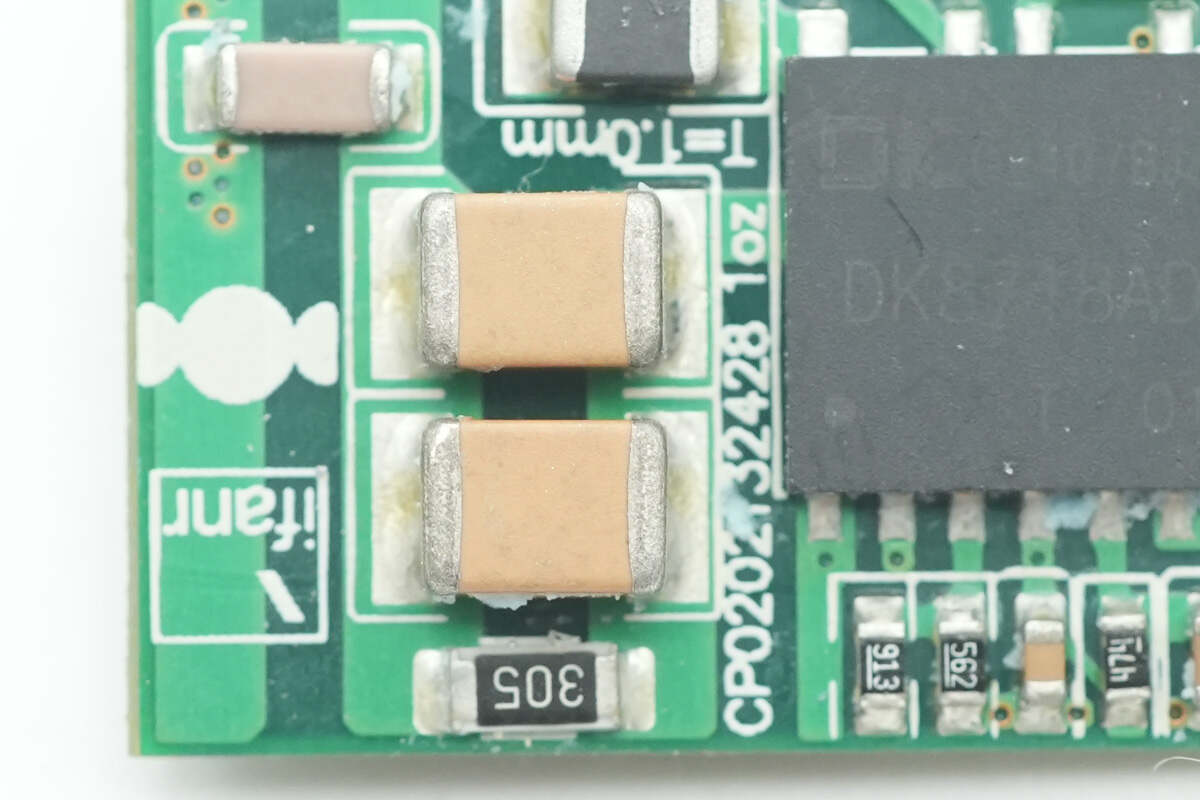
Close-up of two ceramic resonant capacitors connected in parallel.
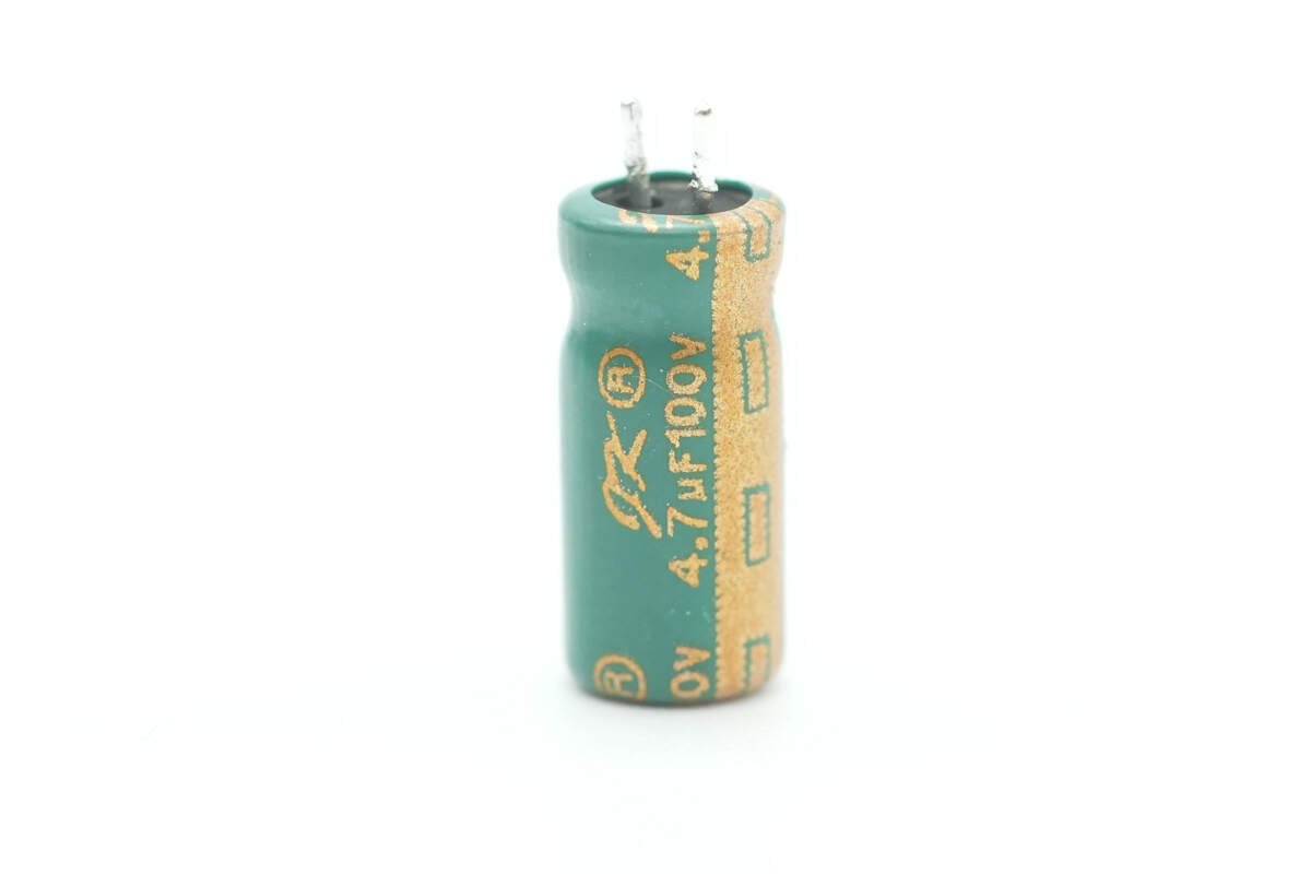
The filter capacitor powering the GaN chip is sourced from JK. 4.7μF 100V.
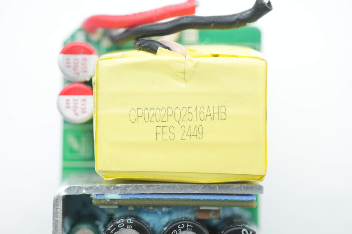
The transformer is insulated with tape wrapped around it.
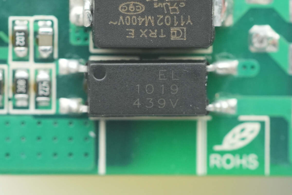
The Everlight EL1019 optocoupler is used for output voltage feedback.
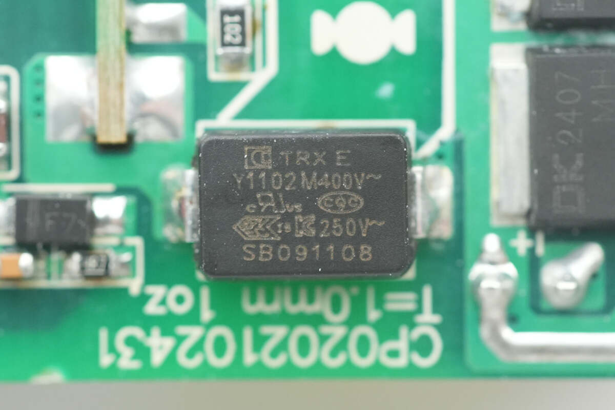
The SMD Y capacitor is from TRX. Its small size and light weight are suitable for high-density power products such as GaN fast chargers. The part number is TMY1102M.
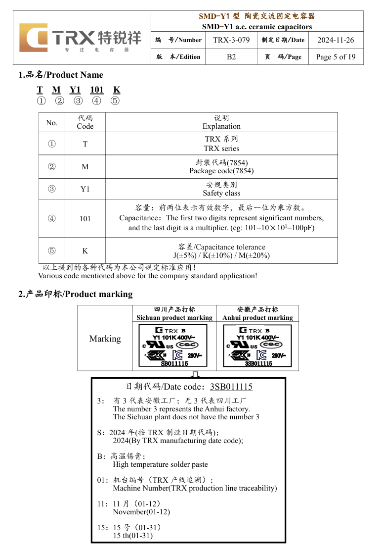
Here is the information about the TRX SMD Y capacitor.
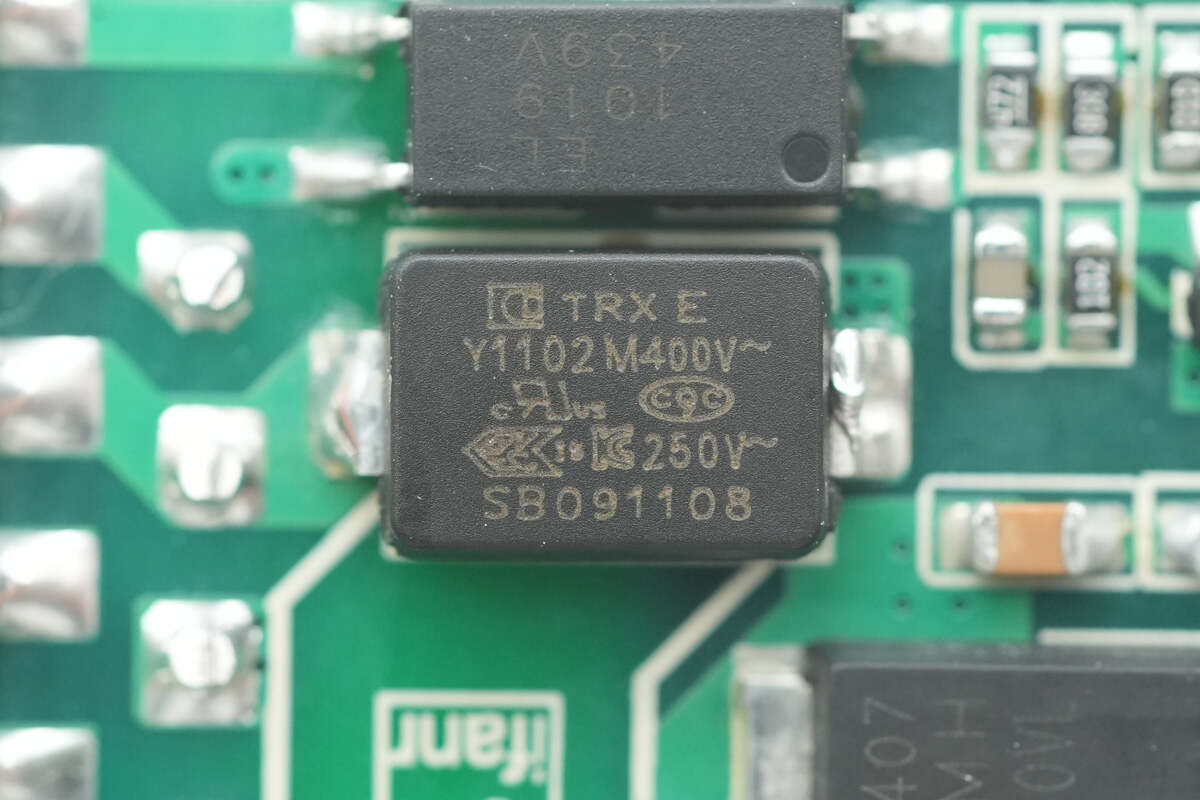
The other SMD Y capacitor has the same part number.
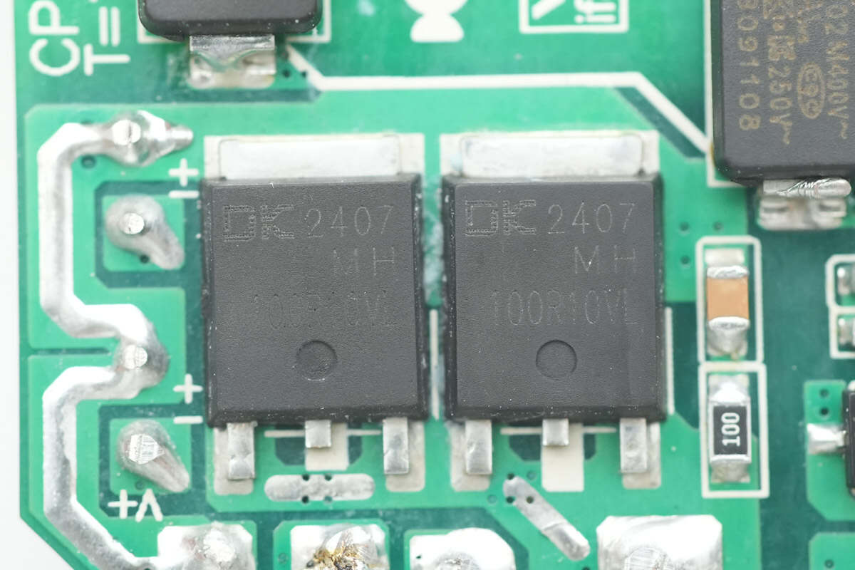
The synchronous rectifier chip is from DONGKE, model DK5V100R10VL. It is a driverless synchronous rectifier chip with an internal 100V voltage rating and 10mΩ on-resistance. It features self-powering technology and can directly replace Schottky diodes. It supports CCM, DCM, and QR operating modes without the need for external components and comes in a TO-252 package.
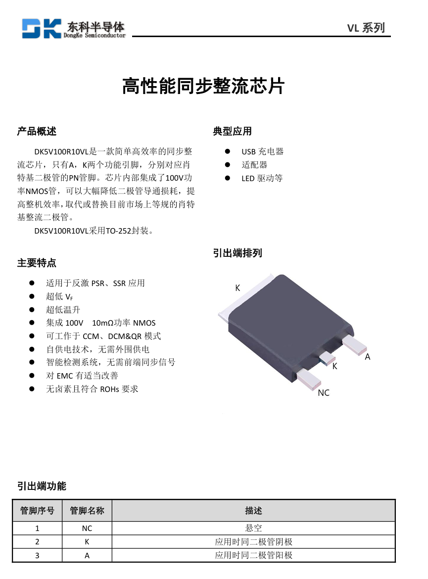
Here is the information about DONGKE DK5V100R10VL.
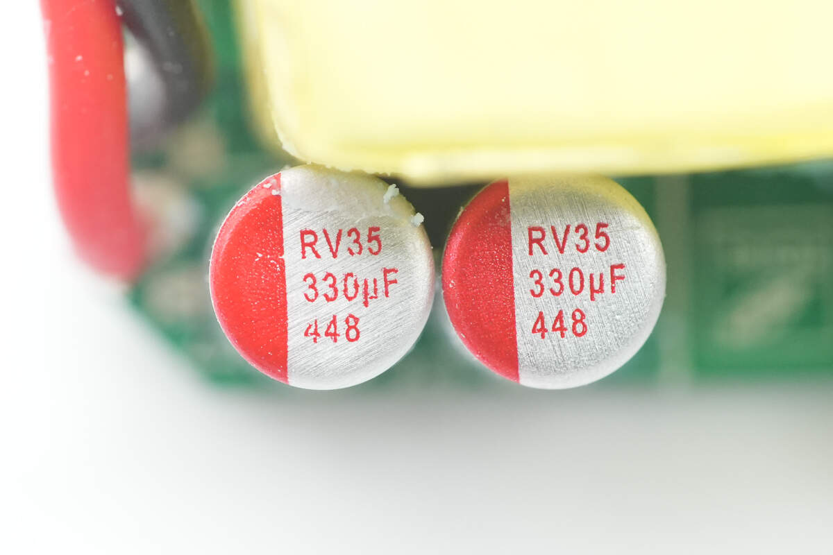
The two filter capacitors are rated at 35V 330μF each.
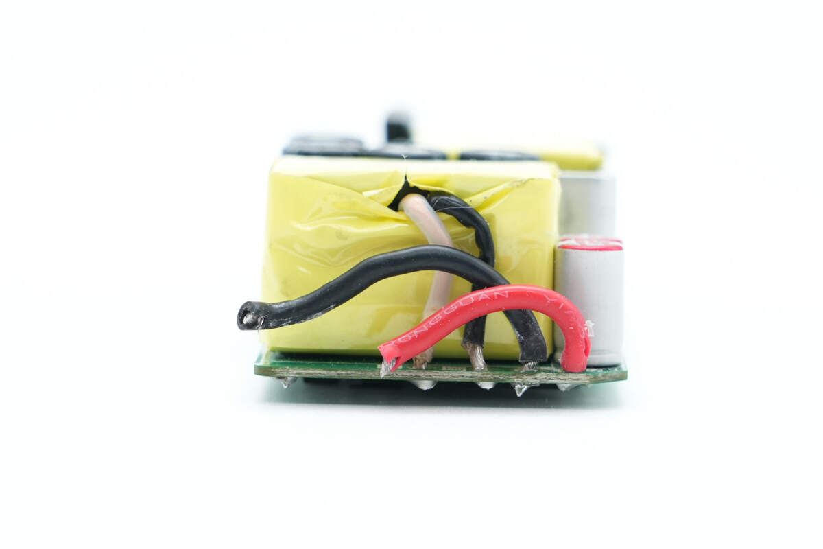
The output end is connected via wiring.
The front and back sides of the buck converter PCB are covered with thermal pads and thermal gel to aid The front and back sides of the buck converter PCB are covered with thermal pads and thermal gel to aid heat dissipation.
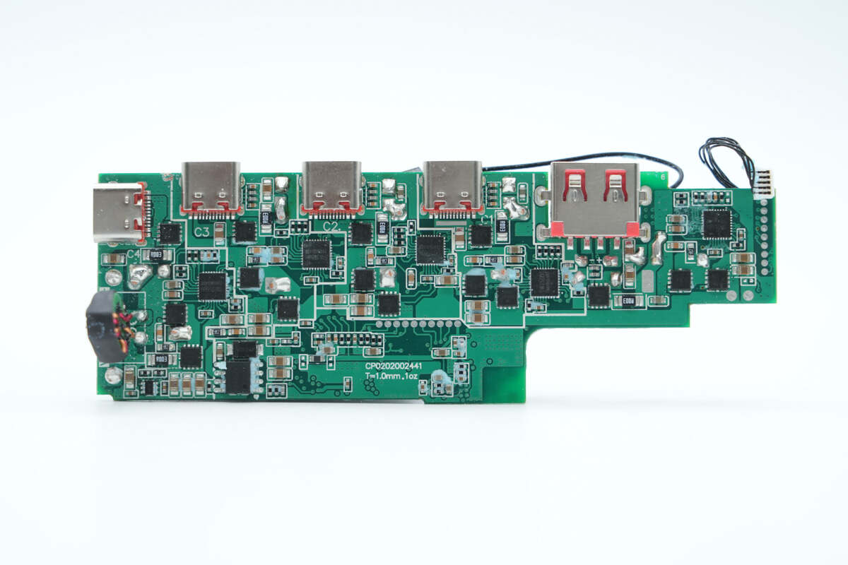
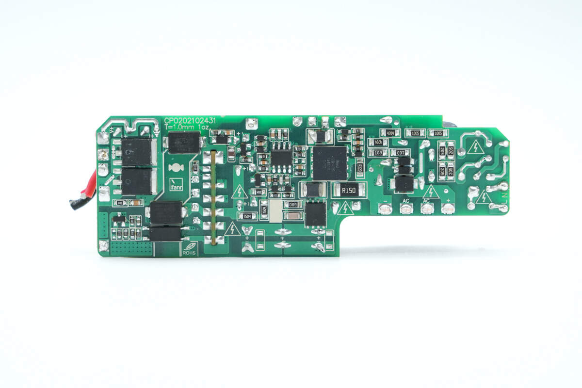
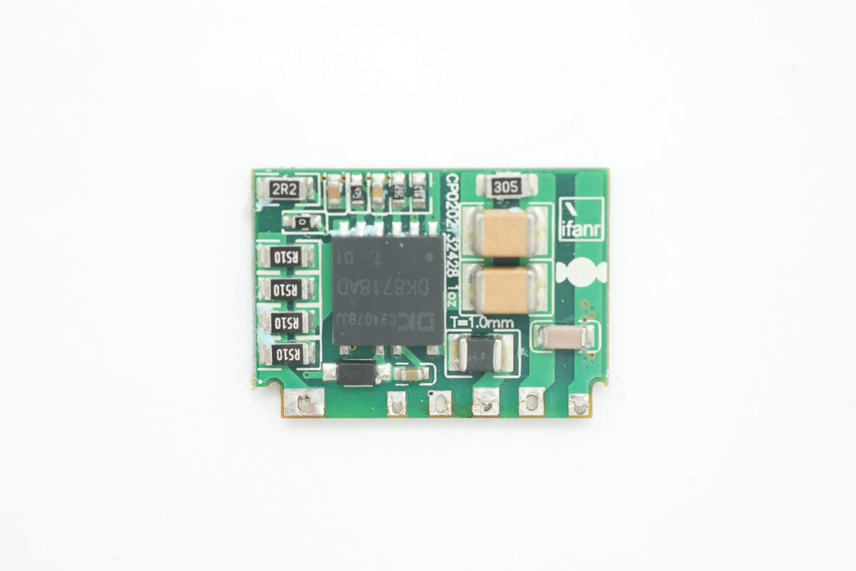
After cleaning, the front side features five secondary buck converter circuits with buck controller chips, synchronous buck MOSFETs, VBUS MOSFETs, and other components.
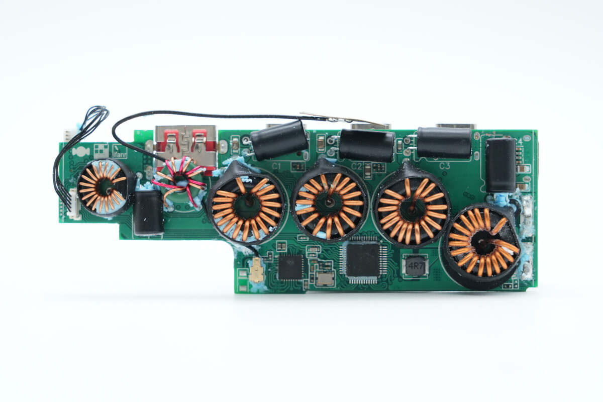
The back side has buck inductors corresponding to the five buck converter circuits, secondary filter solid-state capacitors, an MCU, and other components. All capacitors are insulated and protected with heat shrink tubing.
The input filter inductor is insulated with heat shrink tubing.
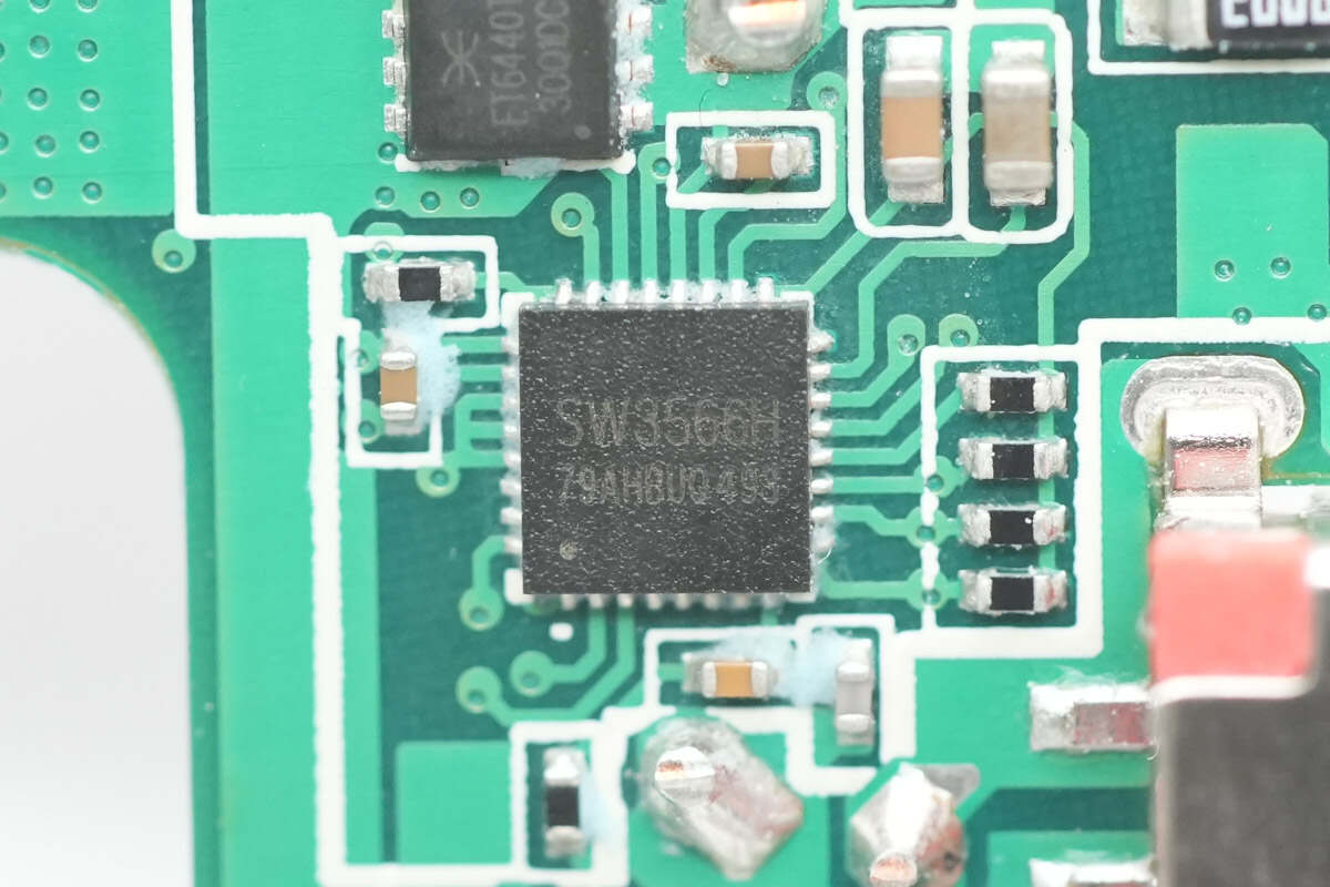
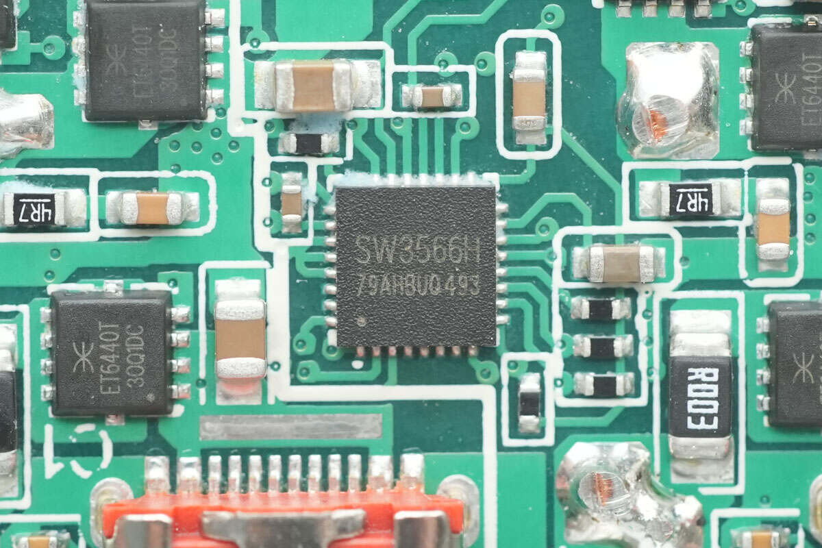
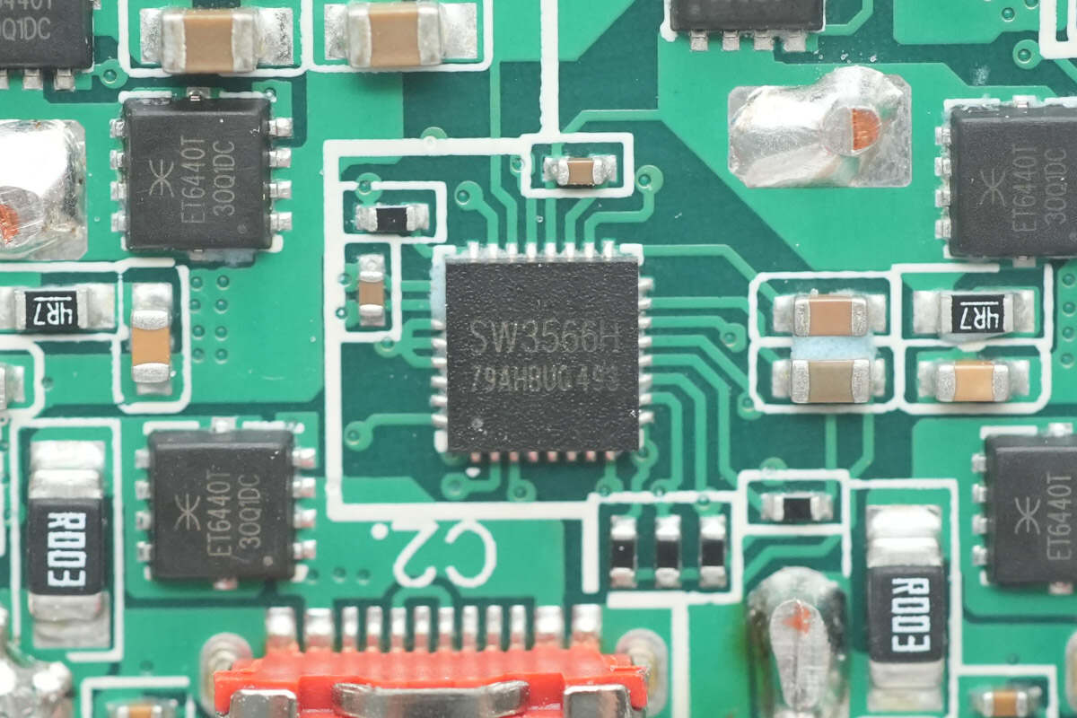
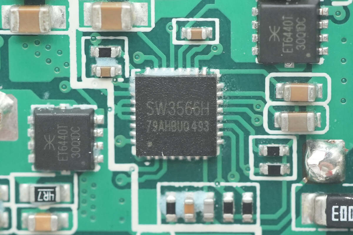
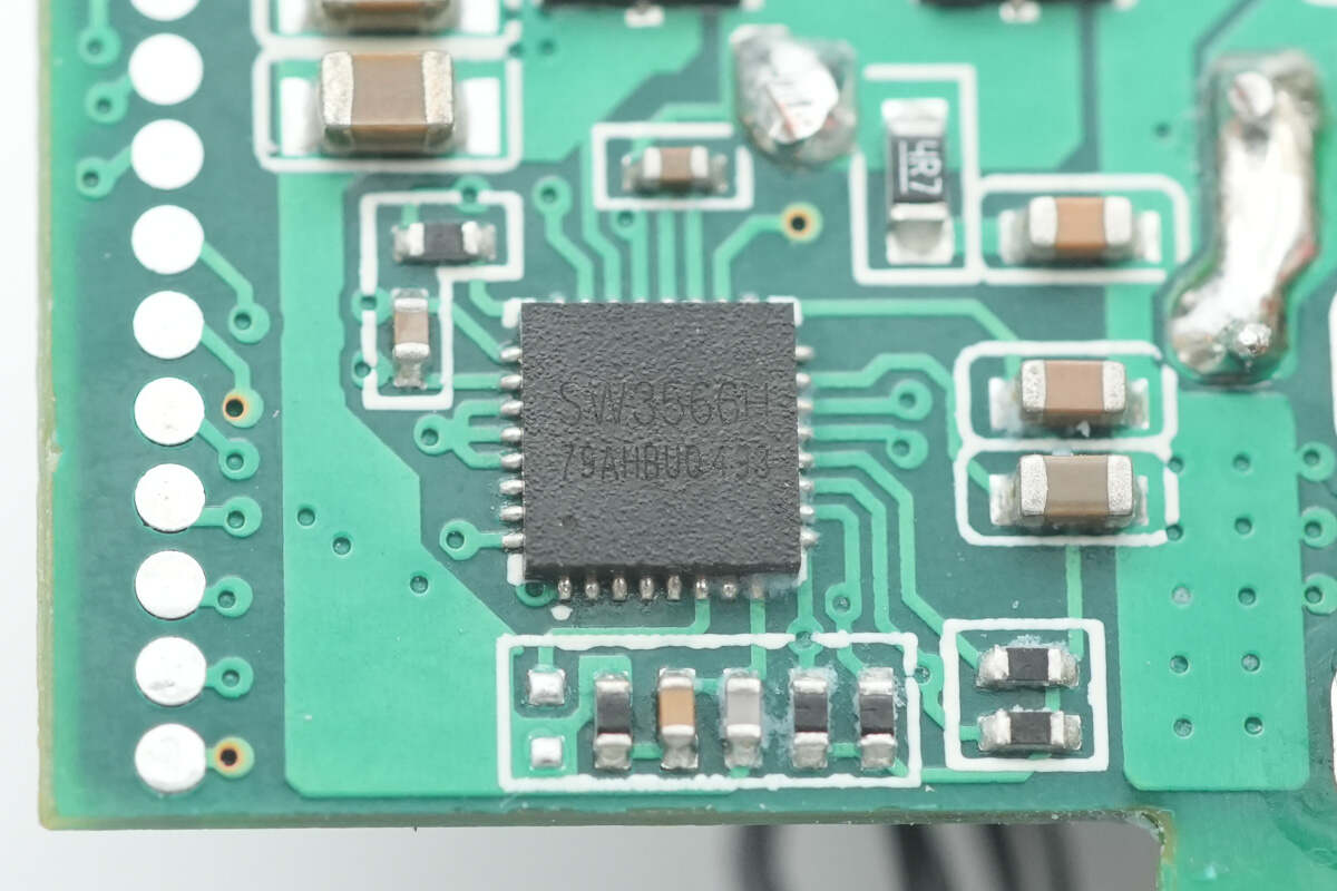
The USB-C1 port uses the iSmartWare SW3566H buck protocol chip, a highly integrated multi-fast-charge dual-port SOC chip that supports charging for both USB-C and USB-A ports with independent current limiting for each port. It integrates a high-efficiency synchronous buck converter supporting 20V/7A and 28V/5A outputs, and fast-charging protocols including PD 3.1, QC, SCP, and UFCS, with customizable fast-charge protocol support and a maximum output power of 140W.
The SW3566H integrates CC/CV mode, dual-port management logic, and bus voltage detection. Paired with corresponding buck MOSFETs and VBUS MOSFETs, it achieves dual-port buck output. The built-in buck converter operates at 180kHz and supports both PWM and PFM modes. Protection thresholds for output current, line loss compensation, and others can be configured via an I2C interface. The built-in ADC supports data sampling for nine channels, including input/output voltage, output current, and chip temperature, and it supports connection to an external MCU for parameter display.
The SW3566H supports 36V input voltage and a maximum output current of 7A. It features soft-start, input overvoltage/undervoltage protection, output overvoltage/undervoltage protection, output overcurrent/short-circuit protection, DP/DM/CC overvoltage protection, chip overheat protection, external NTC thermistor protection, and power limiting protection. The chip is packaged in a QFN 4×4-32 package.
Here is the information about iSmartWare SW3566..
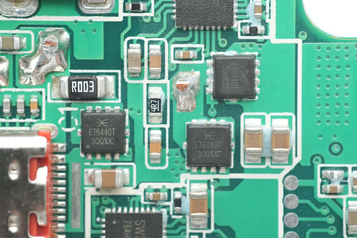
The synchronous buck MOSFETs and VBUS MOSFETs are from Eternal, model ET6440T. They are NMOS transistors with a voltage rating of 40V and an on-resistance of 5.7mΩ, packaged in PDFN3333-8L.
The USB-C2 port uses the iSmartWare SW3566H buck protocol chip.
The USB-C3 port uses the iSmartWare SW3566H buck protocol chip.
The USB-C4 port uses the iSmartWare SW3566H buck protocol chip.
The USB-A port uses the iSmartWare SW3566H buck protocol chip.
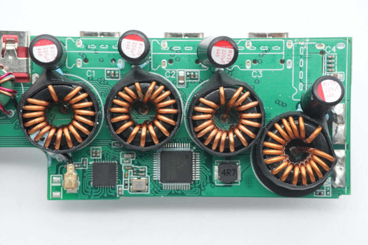
The four USB-C ports use ring-core buck inductors, each insulated with heat shrink tubing.
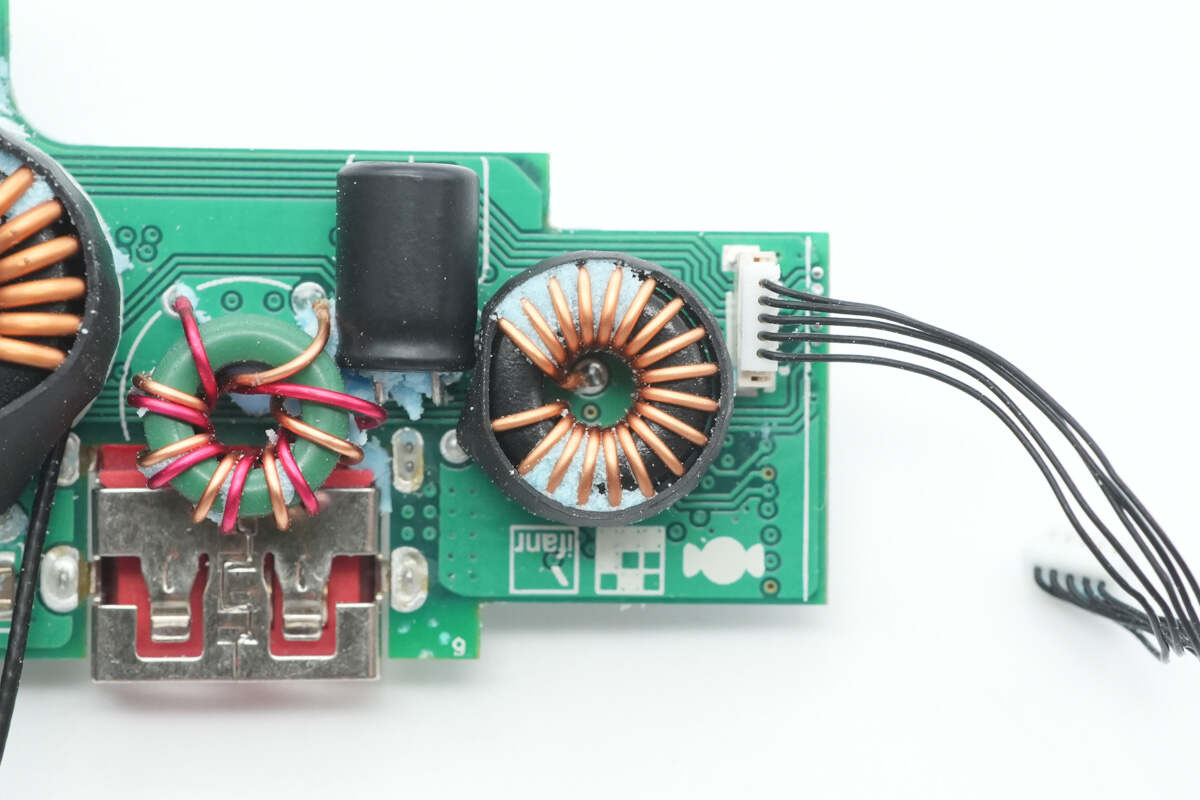
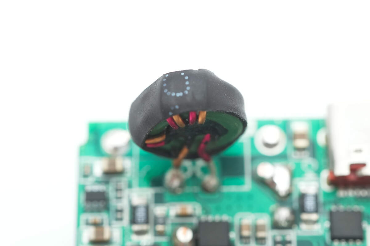
Close-up of the buck inductor of the USB-A port.
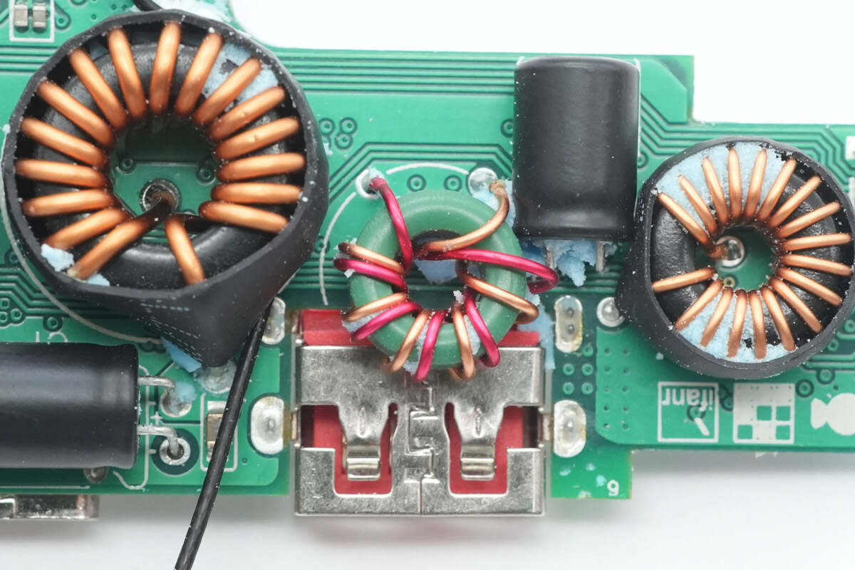
The USB-A port has a magnetic filter inductor.
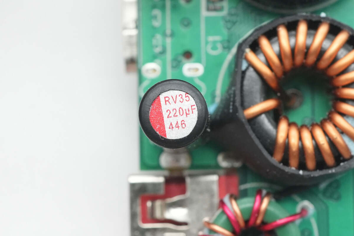
The solid capacitor used for filtering the four USB-C ports has a specification of 35V 220μF.
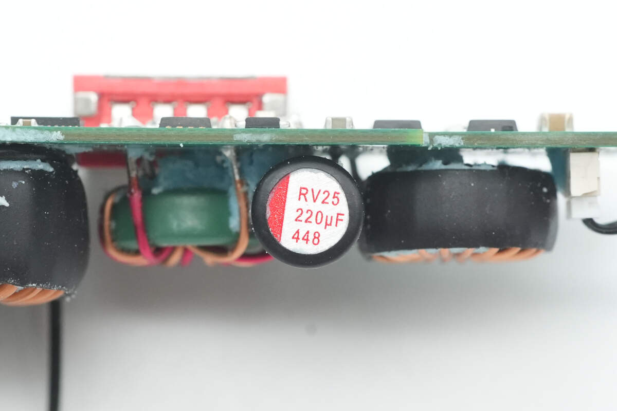
The filtering capacitor specification for the USB-A is 25V 220μF.
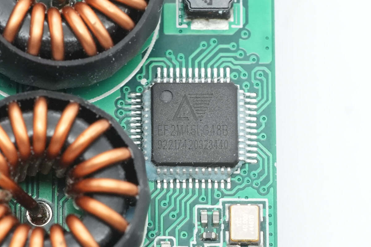
The FPGA chip is from Anlogic, model EF2M45LG48B. It uses a 55nm low-power process, integrates Flash internally, supports multiple configuration modes, and collects input and output information from five SW3566 devices via the I2C bus. It is packaged in an LQFP48 form factor.
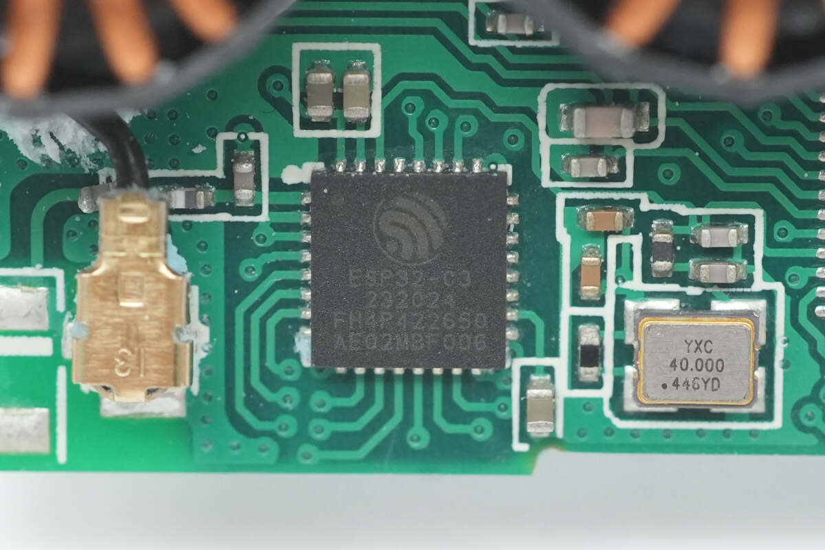
The wireless connectivity chip is from ESPRESSIF, model ESP32-C3. It is a low-power, highly integrated SoC with integrated 2.4GHz WiFi and low-power Bluetooth communication. It features a 160MHz, 32-bit RISC-V single-core processor, 384KB ROM, 400KB SRAM, 8KB SRAM, and a 4Kbit eFuse. It is packaged in a QFN32 form factor.
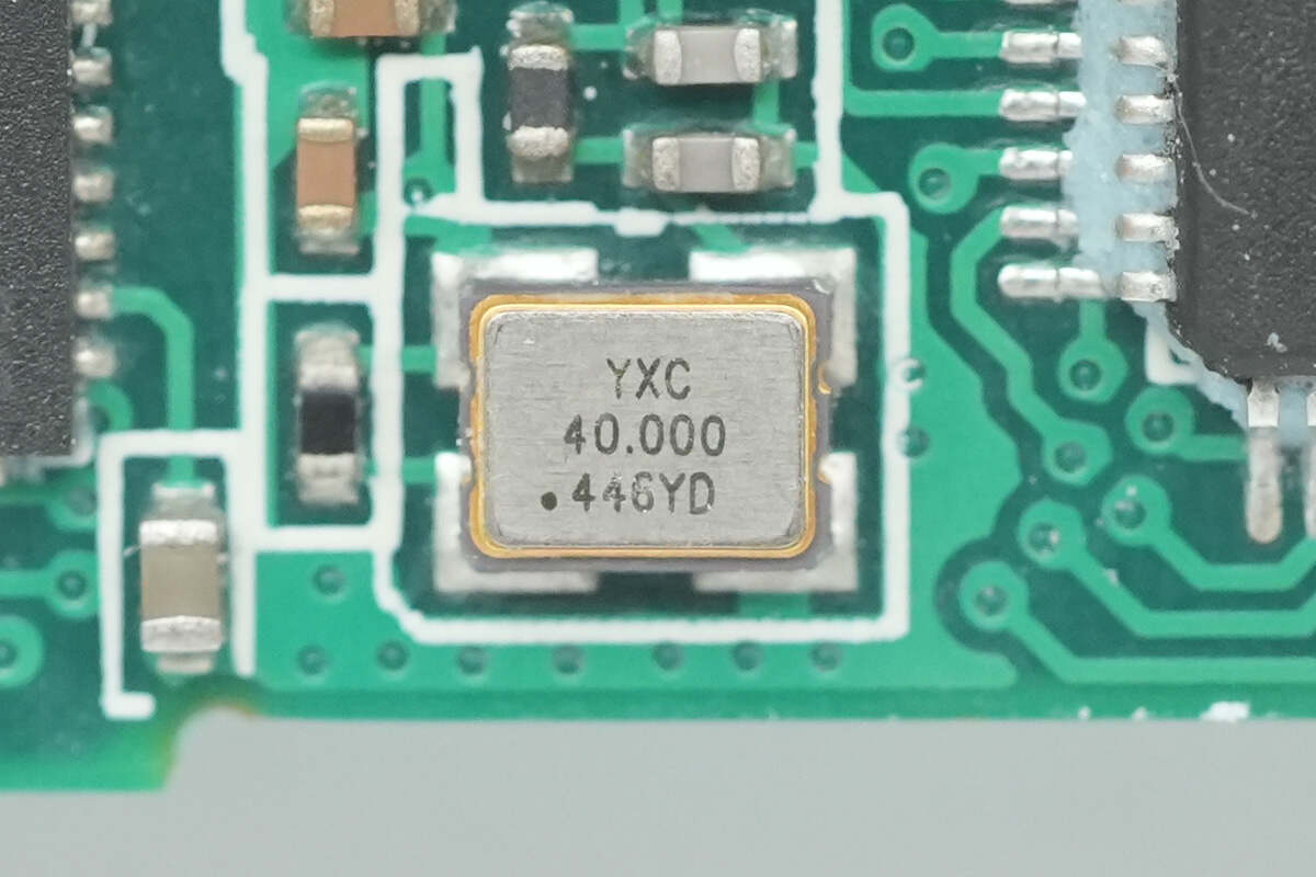
Close-up of the 40.000MHz clock crystal.
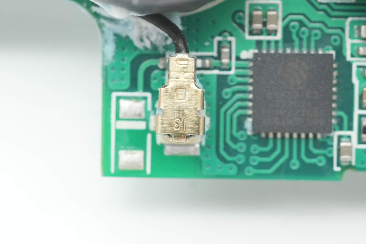
Close-up of the socket used to connect the FPC antenna.
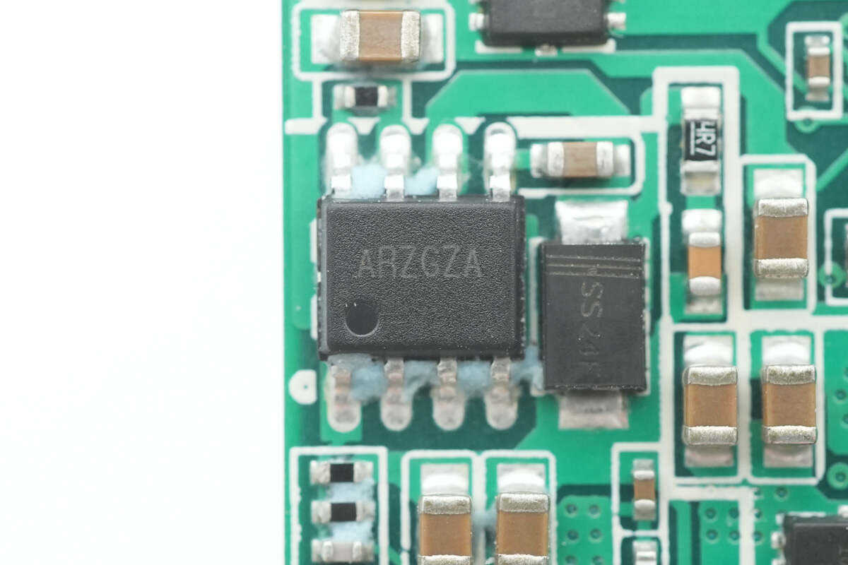
The buck chip is from Silergy, marked with ARZ, and comes in an SOP8 package.
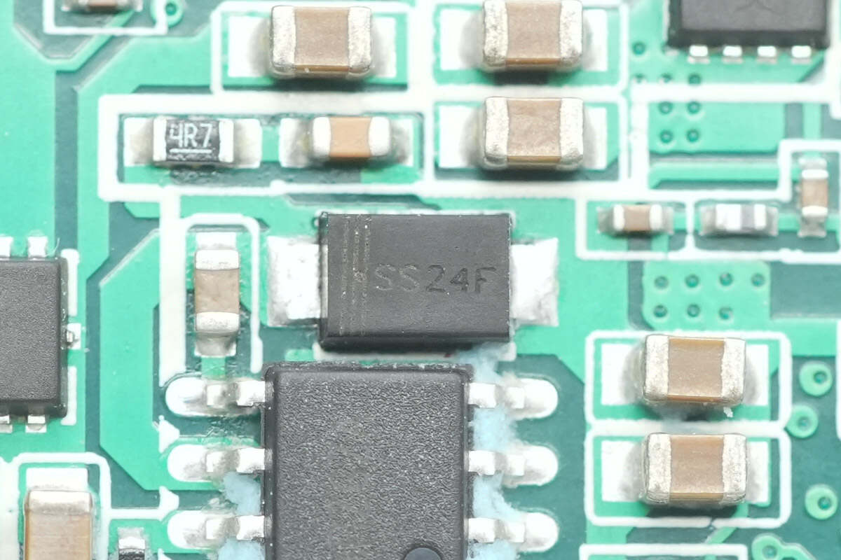
The freewheeling Schottky diode model is SS24F.
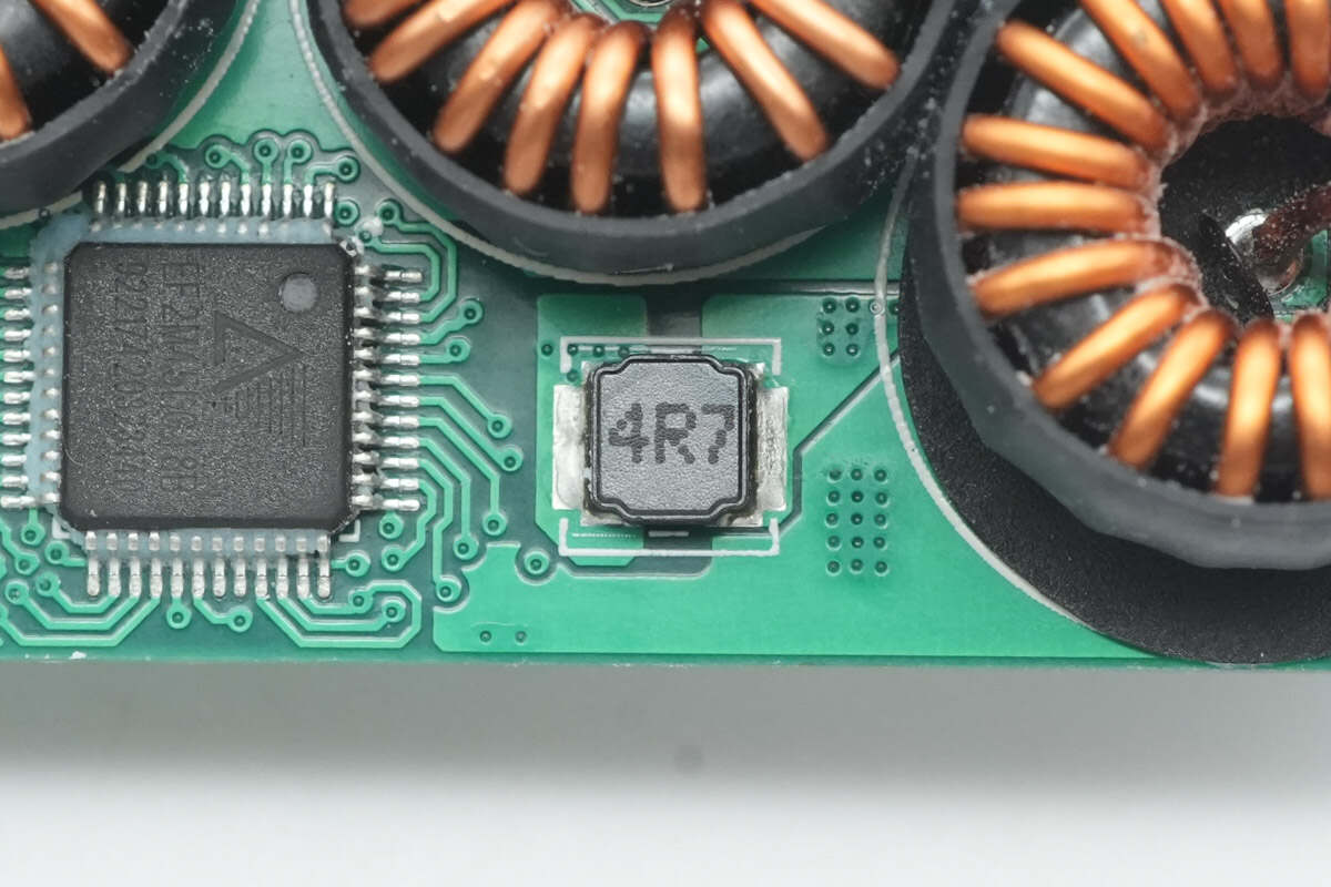
Close-up of the 4.7μH buck inductor.
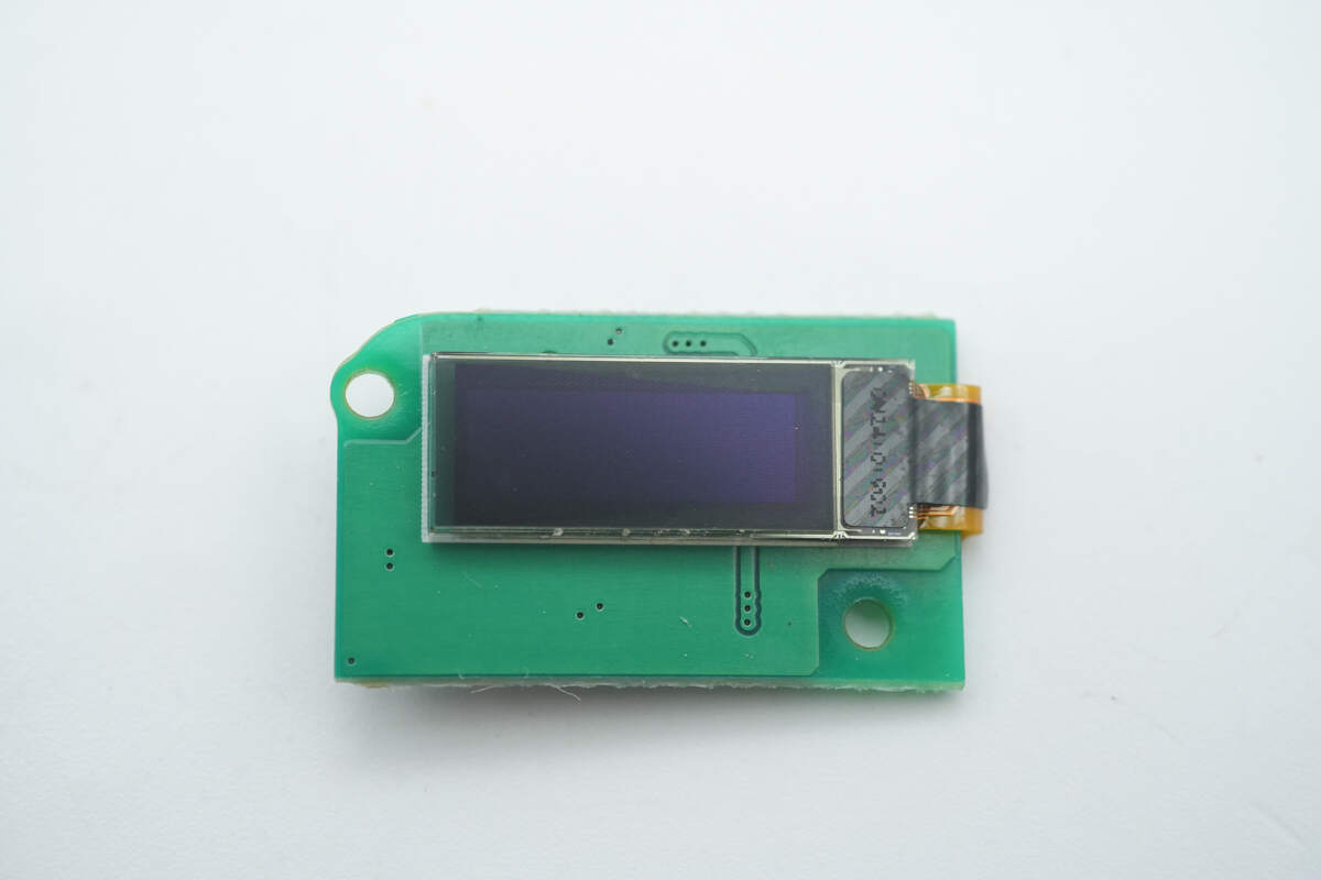
The front of the PCB features an OLED screen.
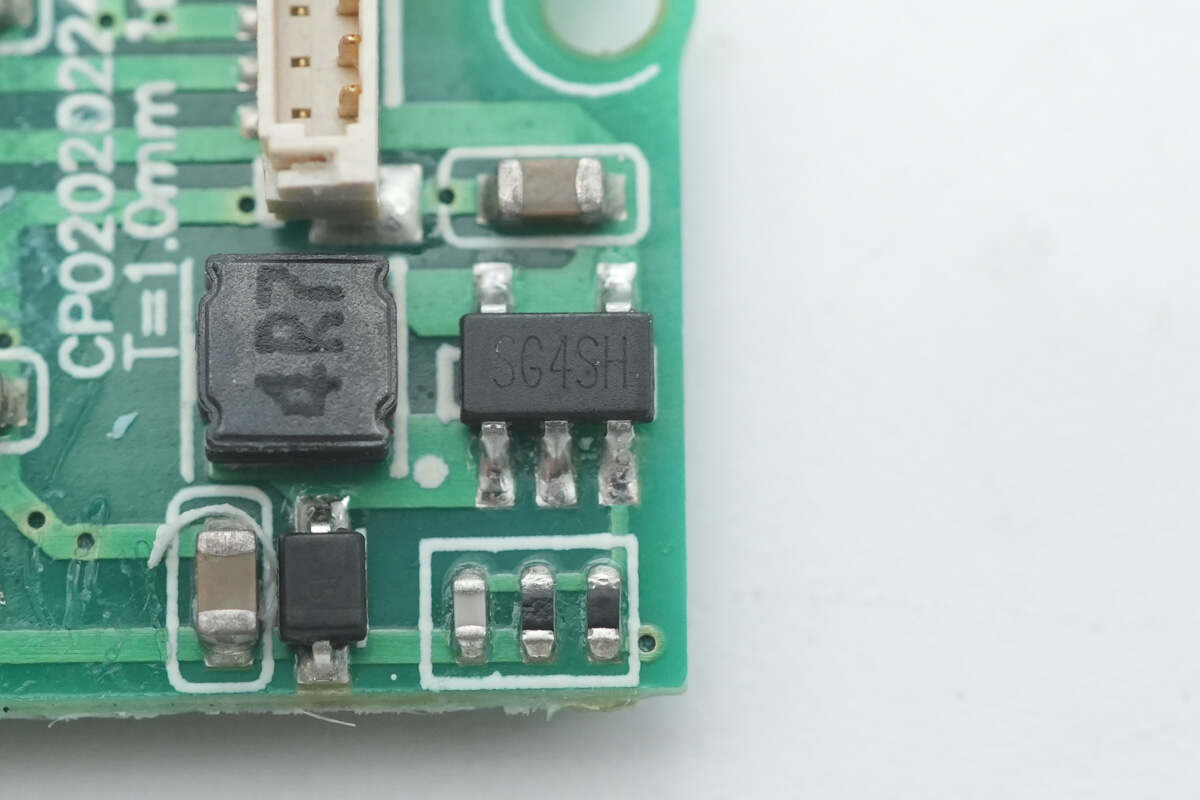
The boost chip is from SGMICRO, marked with SG4, model SGM6601YTN5G. It is a boost chip with an input voltage range of 1.8-5.5V, a maximum output voltage of 38V, and a maximum switching frequency of 1MHz. It comes in a TSOT23-5 package.
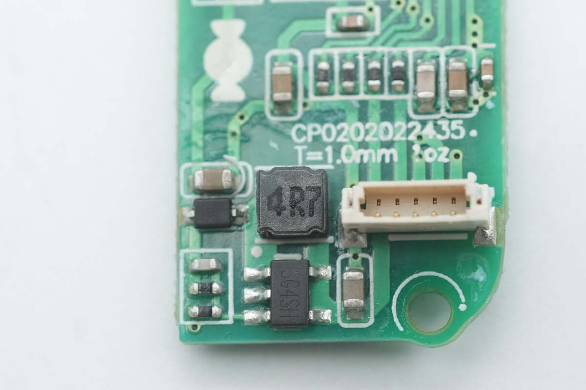
Close-up of the 4.7μH boost inductor.
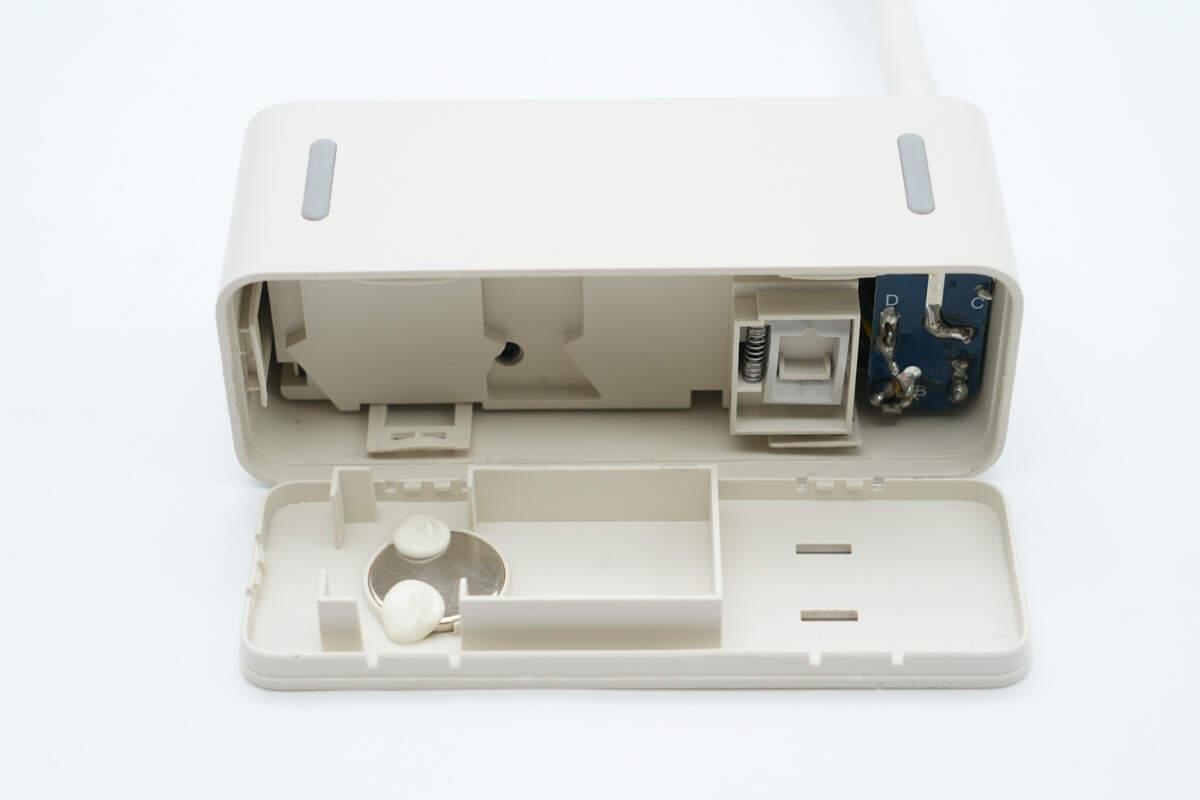
Remove the front cover, which is fixed with buckles.
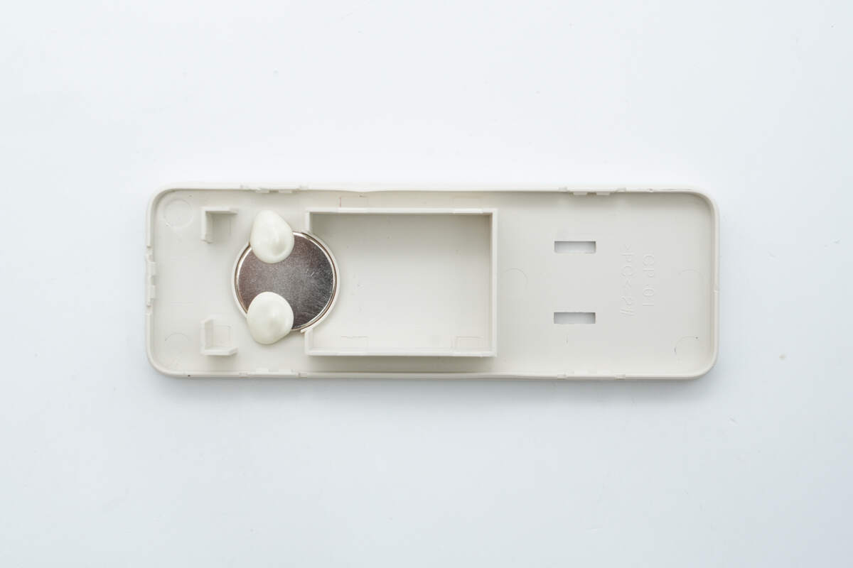
The cover is embedded with a disc-shaped magnet and reinforced with glue.
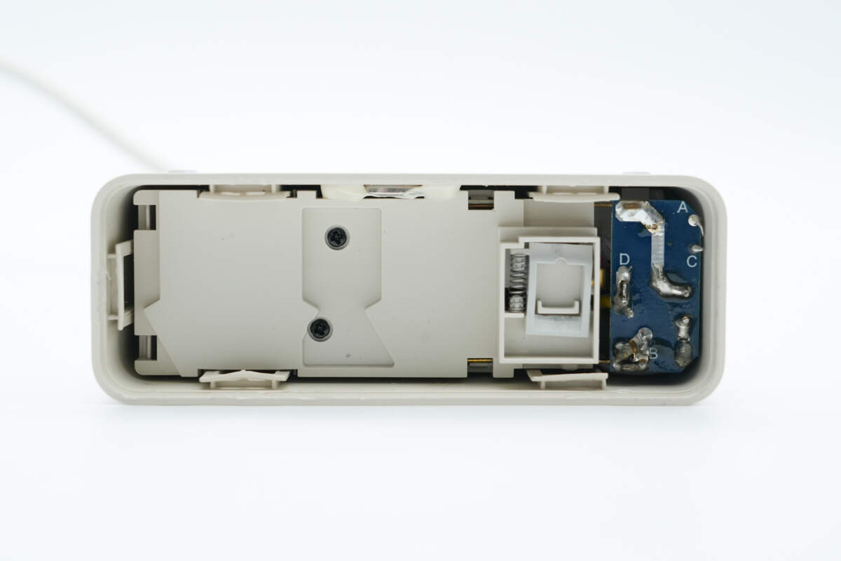
The socket module is fixed with screws, and there is a PCB on the right side.
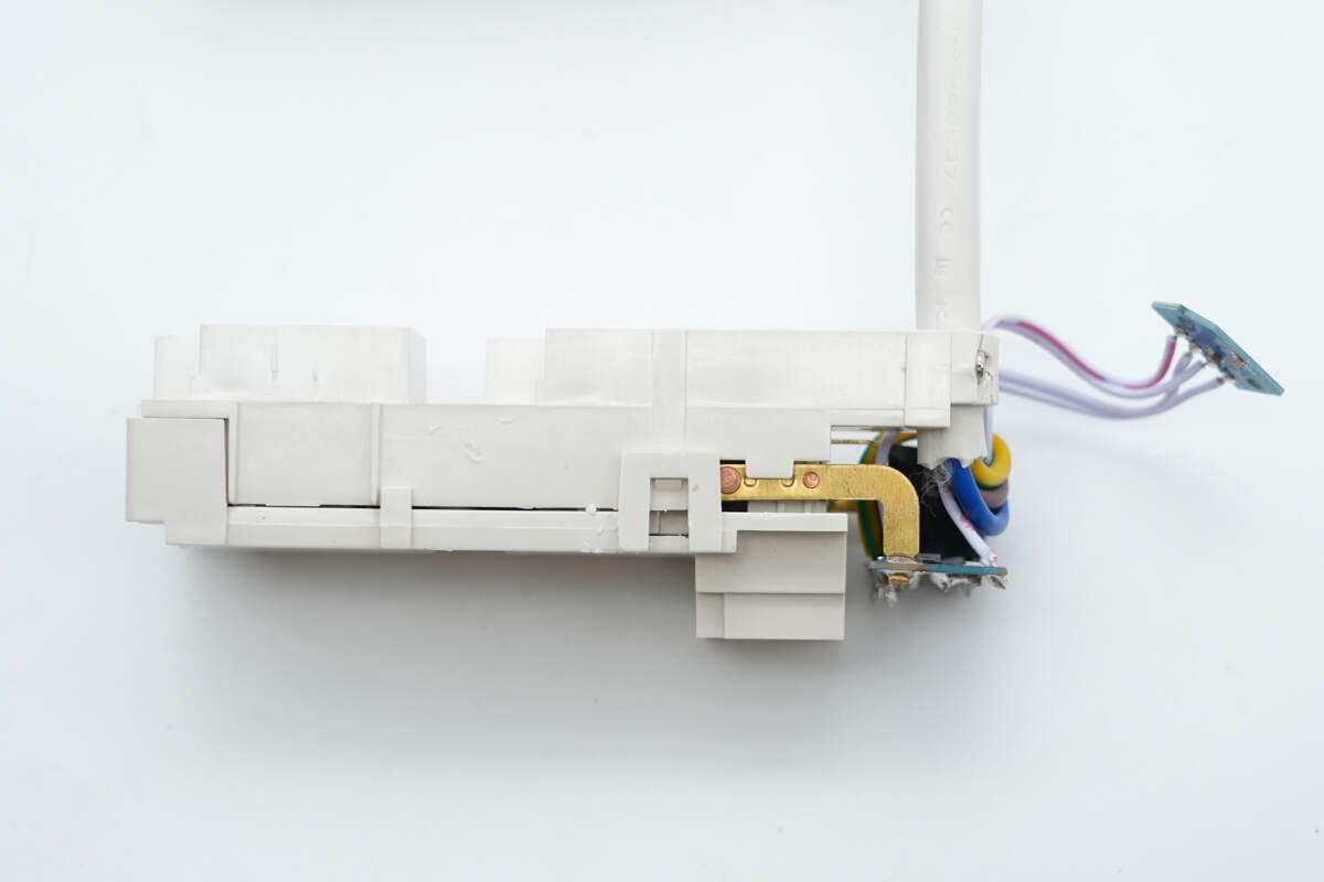
Remove the module, which is also fixed by snaps.
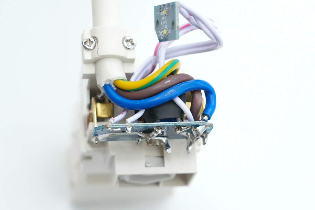
The front of the PCB has a varistor and a thermal fuse for surge protection, both covered with heat-shrink tubing for protection. The power cord is secured with screws and cable clips.
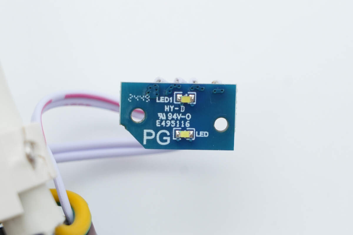
Close-up of the indicator light PCB.

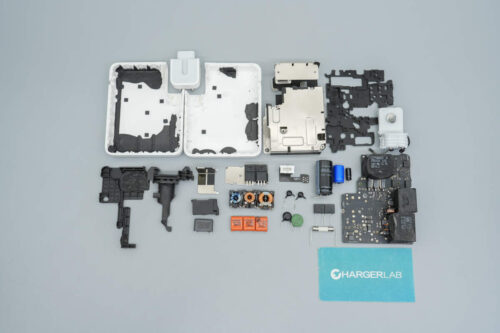
Well, those are all components of the CANDYSIGN 160W CoCan Ultra.
Summary of ChargerLAB
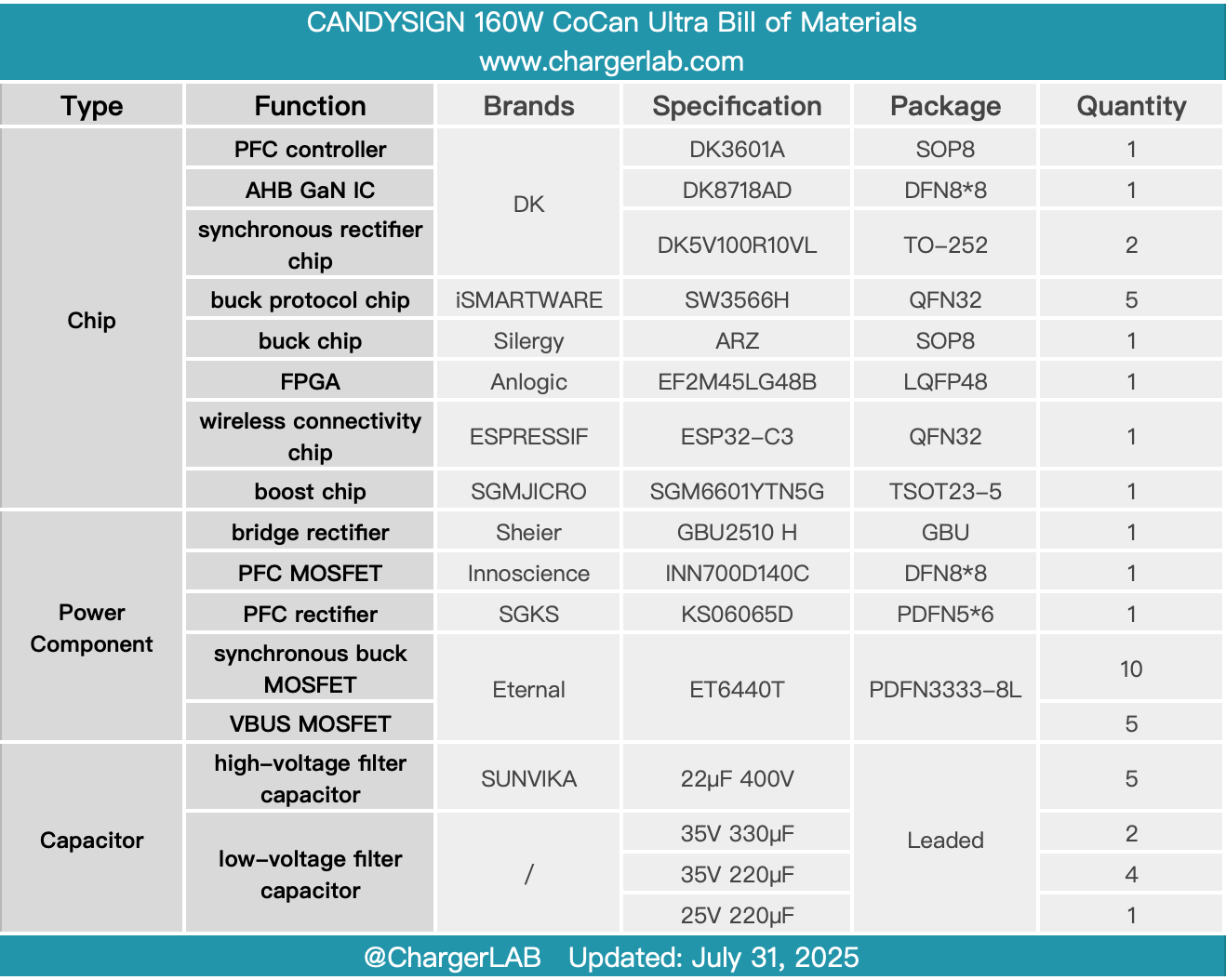
Here is the component list of the CANDYSIGN 160W CoCan Ultra for your convenience.
It features a modular design that combines a power strip and a portable charger. It comes with a 1.5-meter power cord and built-in surge protection. The charger module includes four USB-A ports and one USB-C port, with a total output power of 160W, and supports automatic power distribution.
After taking it apart, we found that it consists of two PCBA modules: the power PCB and the buck PCB. The power PCB uses the DONGKE DK3601A PFC controller paired with the Innoscience INN700D140C GaN FET and SGKS KS06065D silicon carbide diode to form a PFC boost circuit. The AHB uses the DK8718AD GaN integrated chip, and synchronous rectification is achieved with two DK5V100R10VL in parallel.
The buck PCB uses five iSmartWare Technology SW3566H buck protocol chips combined with Eternal ET6440T MOSFETs, which are used for the four USB-C ports and the USB-A port. It also contains the Anlogic EF2M45LG48B FPGA chip and the ESPRESSIF WSP32-C3 wireless chip. The PCBA modules are enhanced with copper sheets and thermal pads to improve heat dissipation, insulated with high-temperature tape, and the solid capacitors are covered with heat-shrink tubing for insulation. Inside the enclosure, graphite thermal pads are applied, and gel is used to strengthen heat dissipation, ensuring stability during long-term operation.pplied, and gel is used to strengthen heat dissipation, ensuring stability during long-term operation.
Related Articles:
1. Teardown of Baseus 65W GaN5 Pro Charger (CCGAN65C5)
2. Teardown of Delta 240W PD3.1 USB-C Power Adapter
3. Teardown of Ford 1760W Portable EV Charger