Introduction
We have received the BricBloc all-in-one charger — the world’s first fast charging and storage solution that uses a Pogo Pin + magnetic connection design. It integrates charging, storage, and expansion functions, supports 10Gbps high-speed data transfer, and offers 4K 60Hz HDMI output. When connected to a laptop or mini PC via a USB-C interface, it enables external hard drive access, display expansion, and peripheral connectivity.
This solution adopts a modular, split-type design, consisting of a 67W GaN fast charging module, a 512GB/1TB portable SSD module, and a four-port expansion docking station module. The modules connect via 24K gold-plated Pogo Pins and magnetic alignment. The three modules can be freely combined and used in single-layer, double-layer, or triple-layer configurations, allowing flexible switching based on actual usage needs. Next, let’s take a look at the internal design and system architecture.
Product Appearance
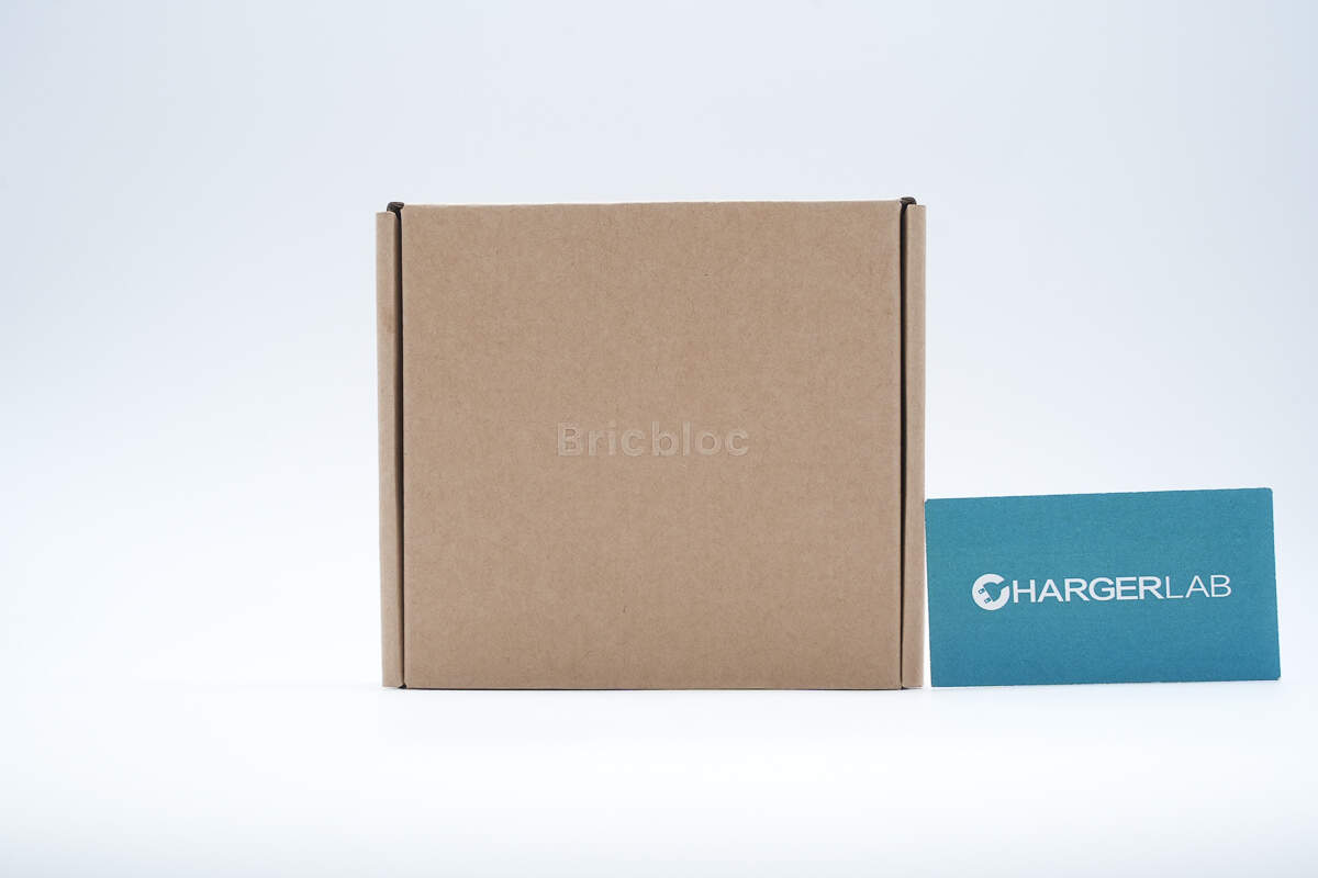
Kraft paper box packaging with the BricBloc logo printed on the front.
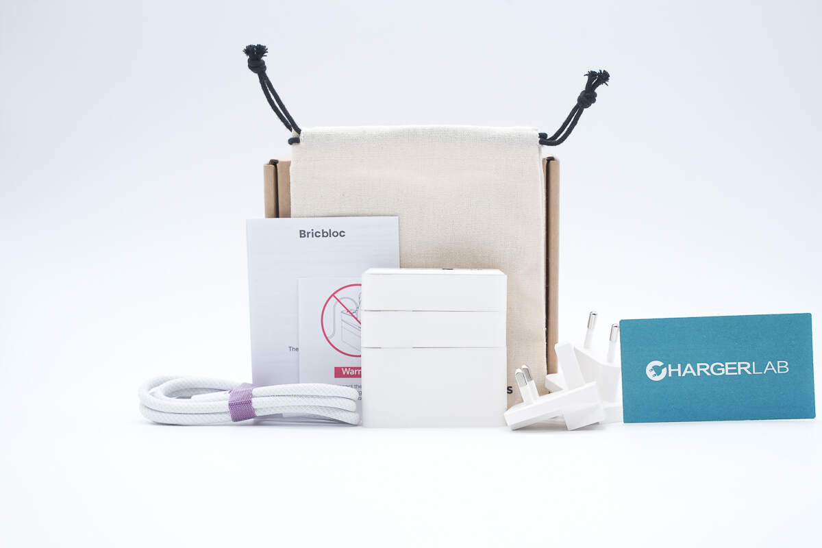
The box includes the charger, data cable, adapter plugs, storage pouch, and user manual.

The storage pouch is printed with the Harbor Innovations logo.
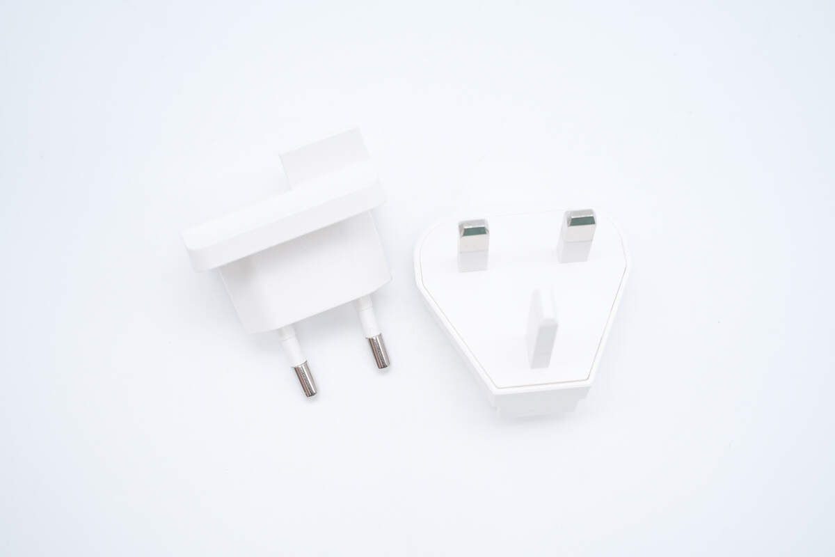
It comes with EU and UK plug adapters.
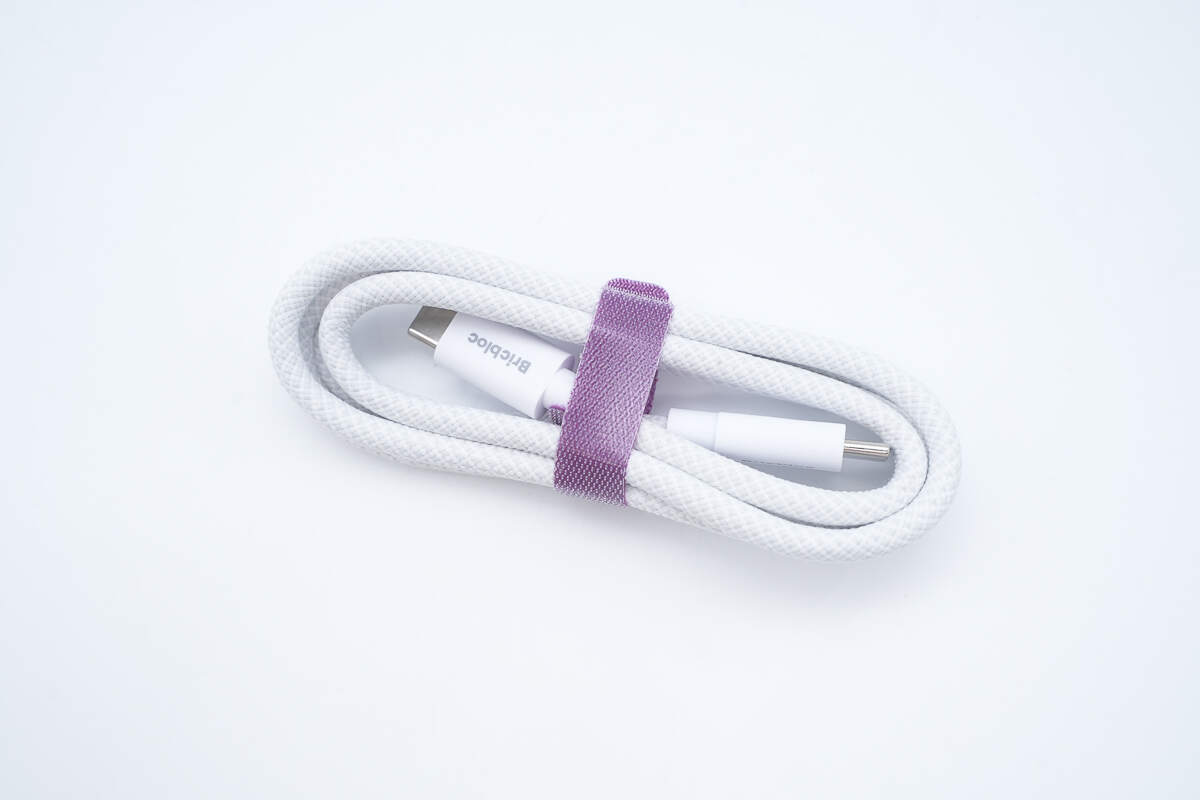
The data cable is braided.
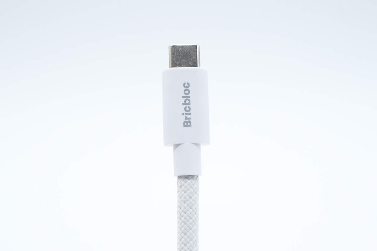
The connector is printed with the BricBloc logo.

The length of the cable is about 100 cm (39.37 inches).
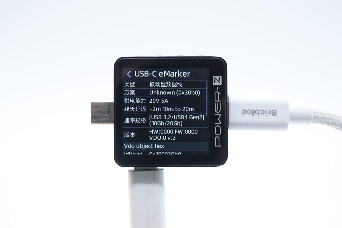
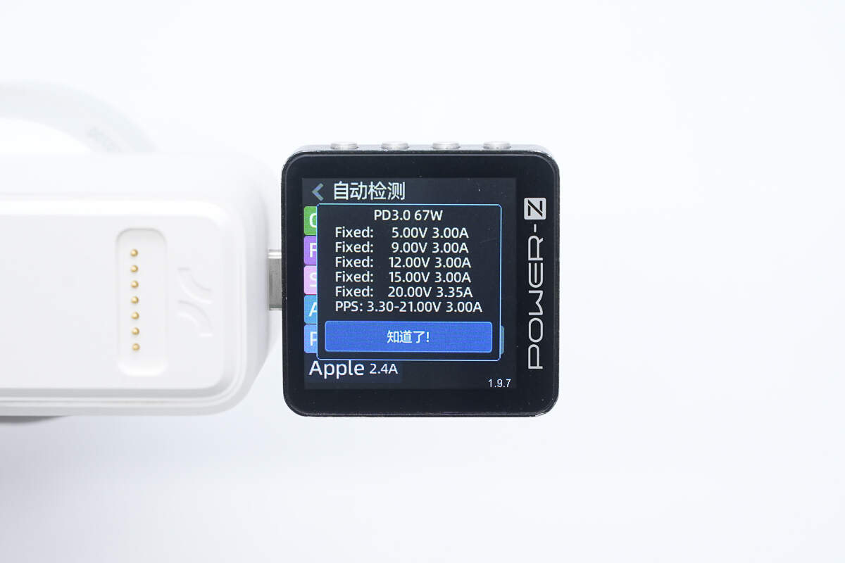
ChargerLAB POWER-Z KM003C shows that it has an E-Marker chip, supporting power delivery of 20V/5A and data transfer speeds of USB4 Gen 2 at 20Gbps.
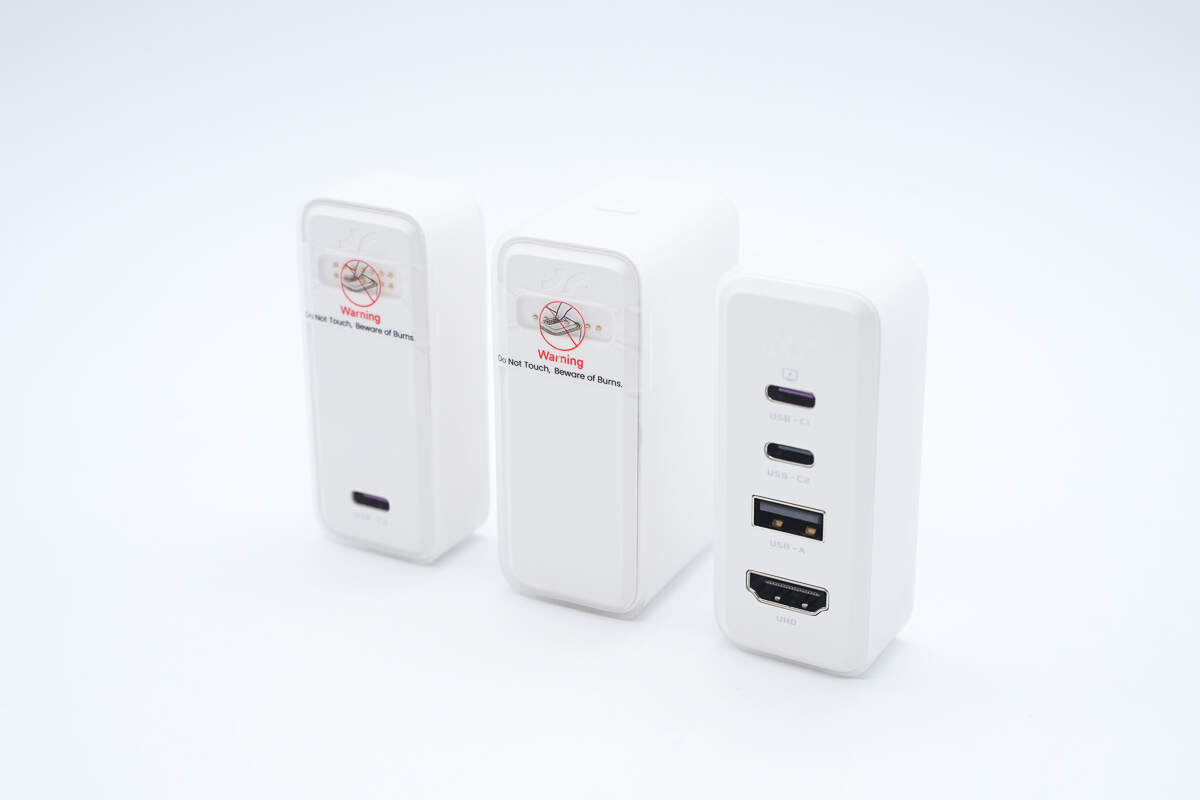
An overview of the 512GB portable SSD module, the 67W GaN fast charging module, and the four-port expansion docking station module. The modules connect through 24K gold-plated Pogo Pin contacts.
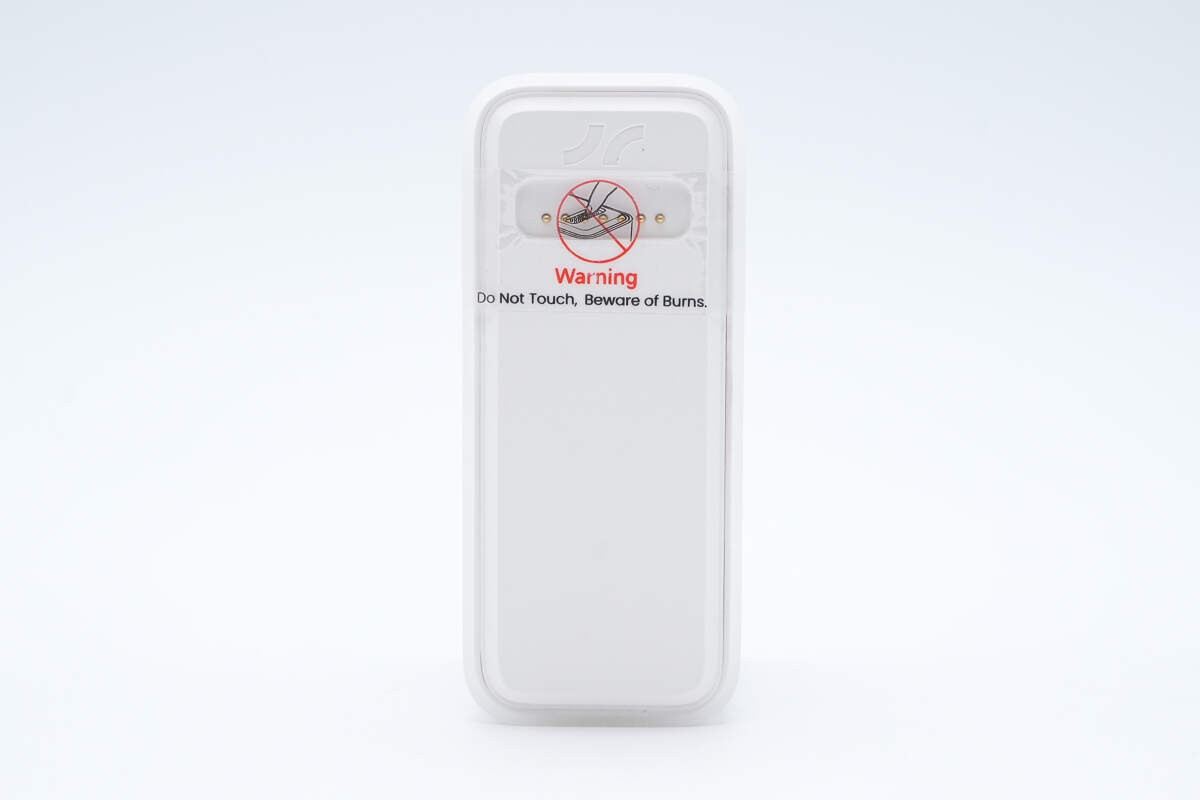
The SSD module is equipped with Pogo Pin contacts and a USB-C female port.
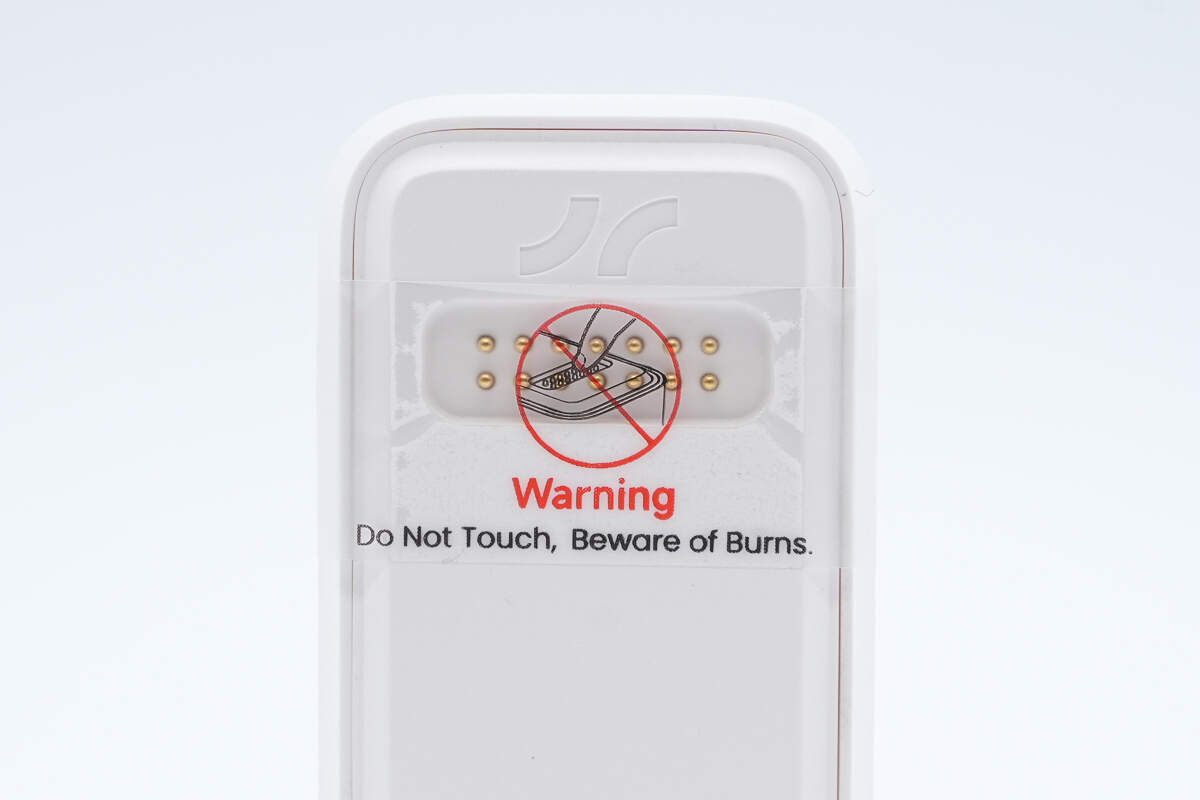
A protective sticker is applied to the contacts.
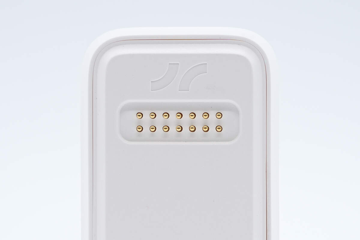
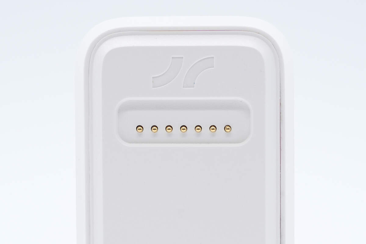
Close-up of the contacts.
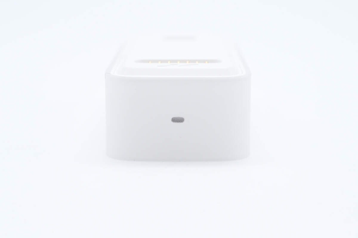
There is an LED indicator light on the bottom.
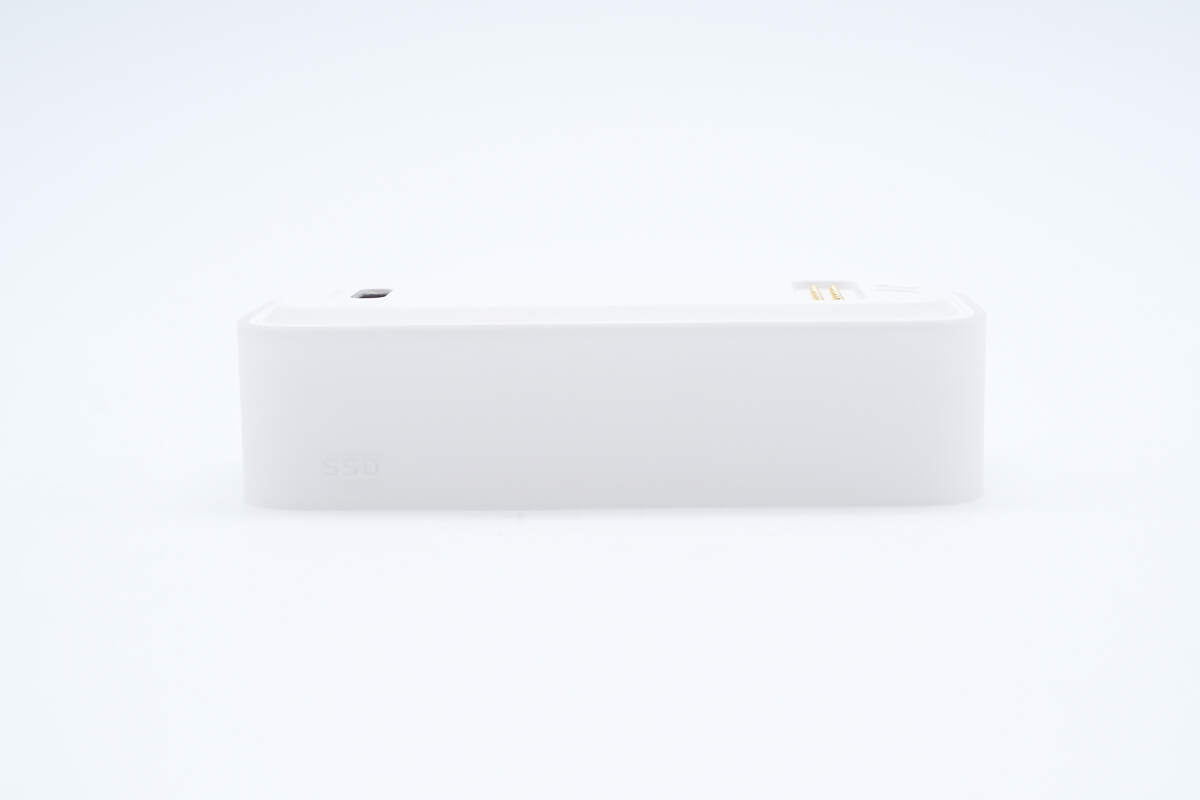
The side is labeled with "SSD."
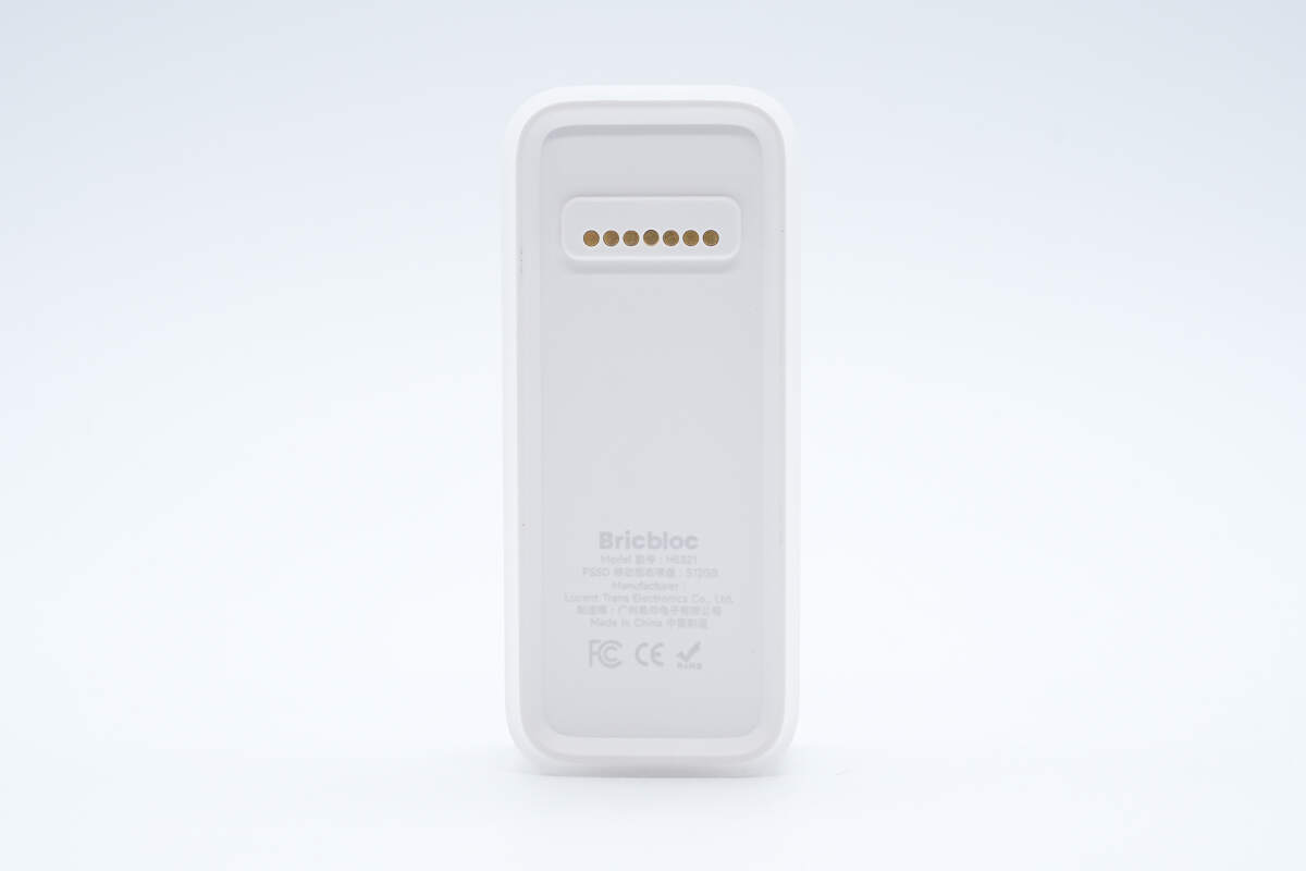
Inside, there are Pogo Pin contacts and a nameplate.
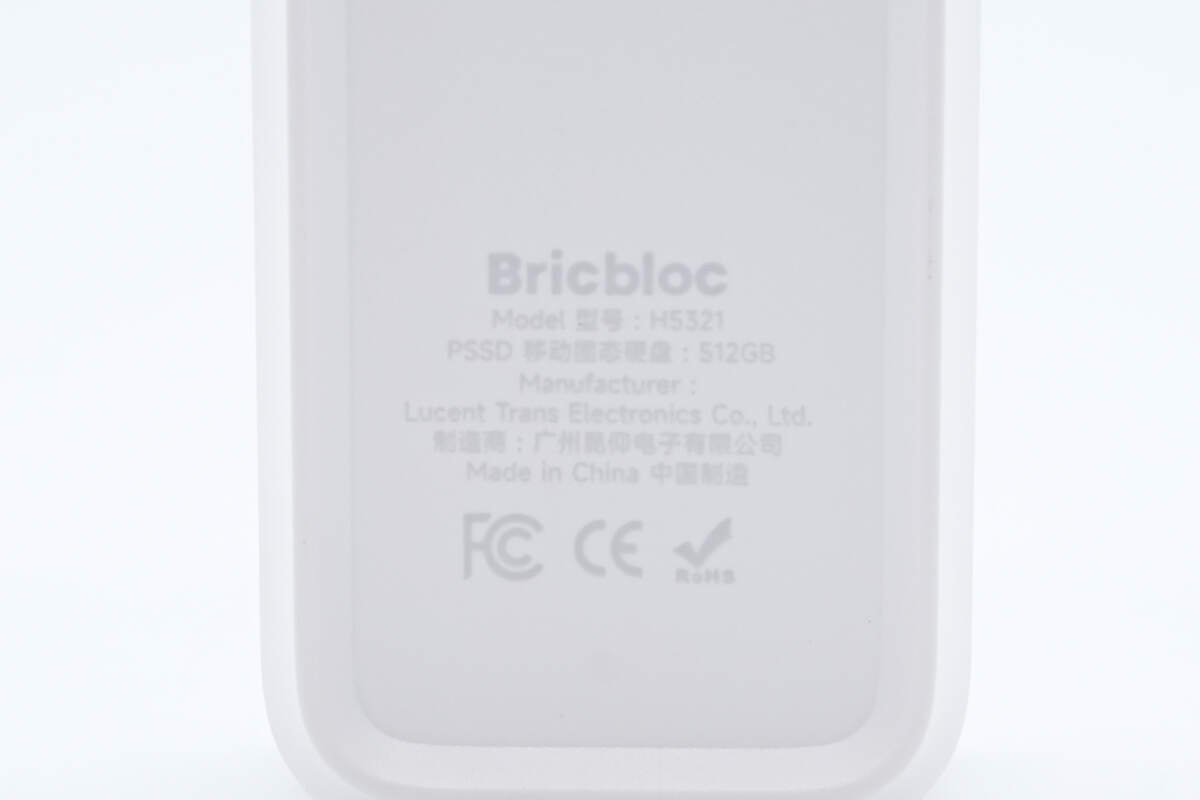
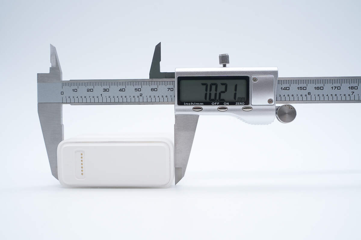
Model H5321 with a capacity of 512GB.
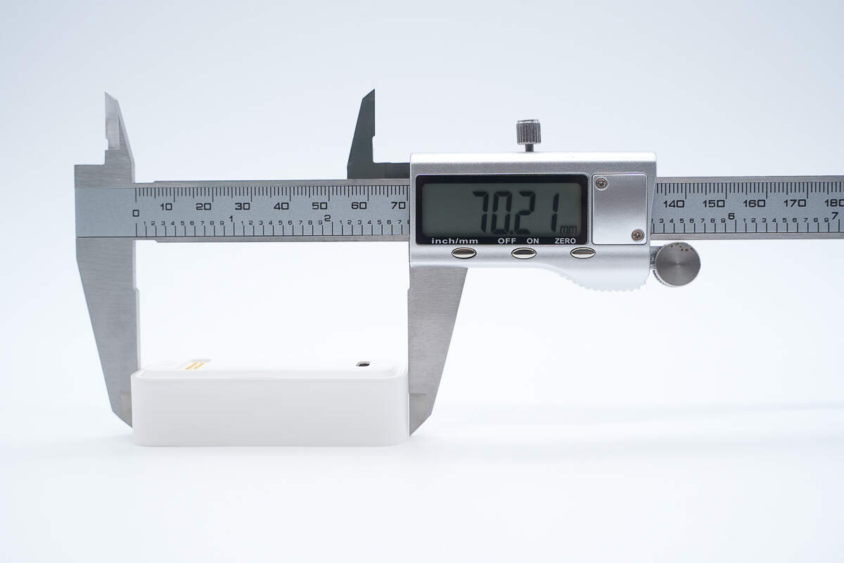
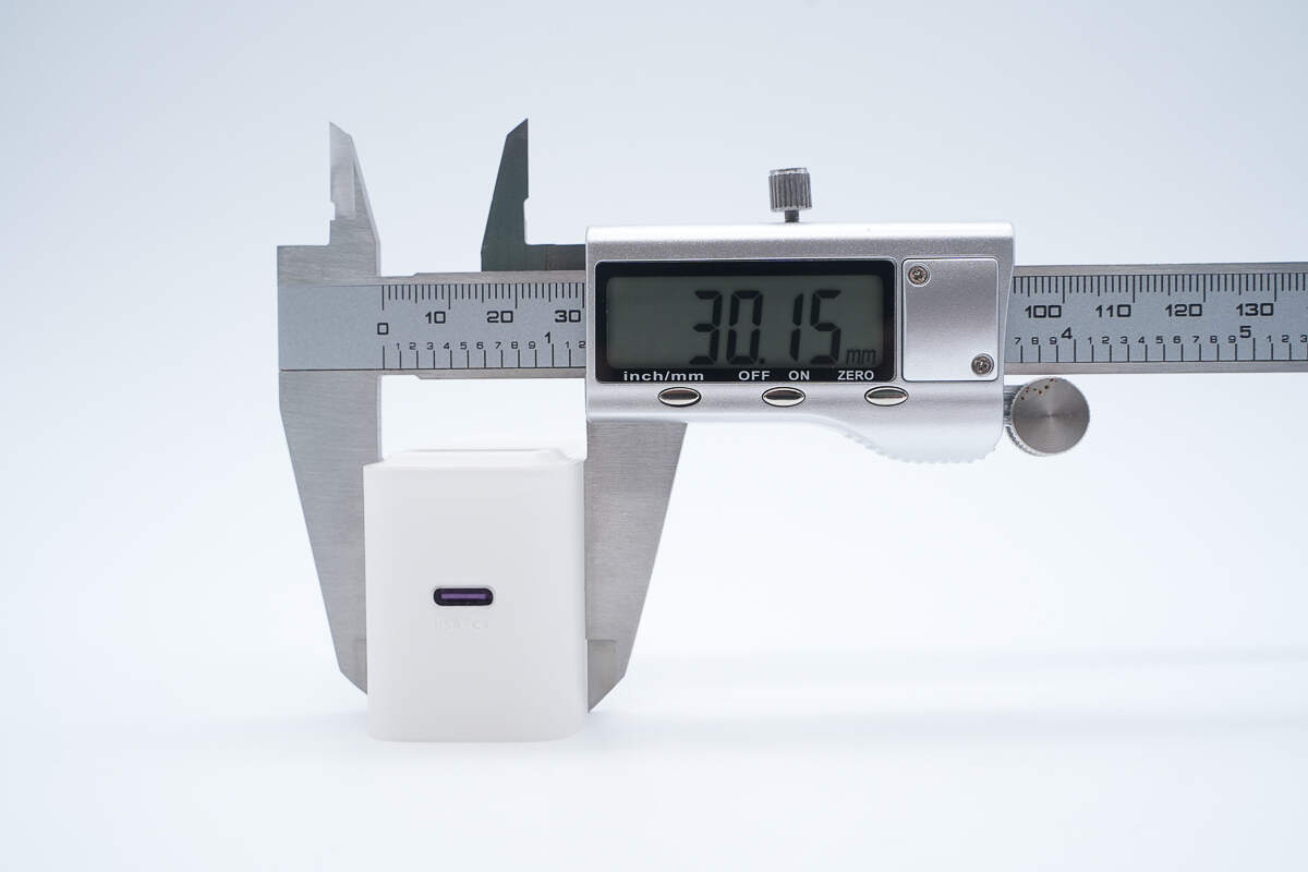
The length is about 70.2 mm (2.76 inches).
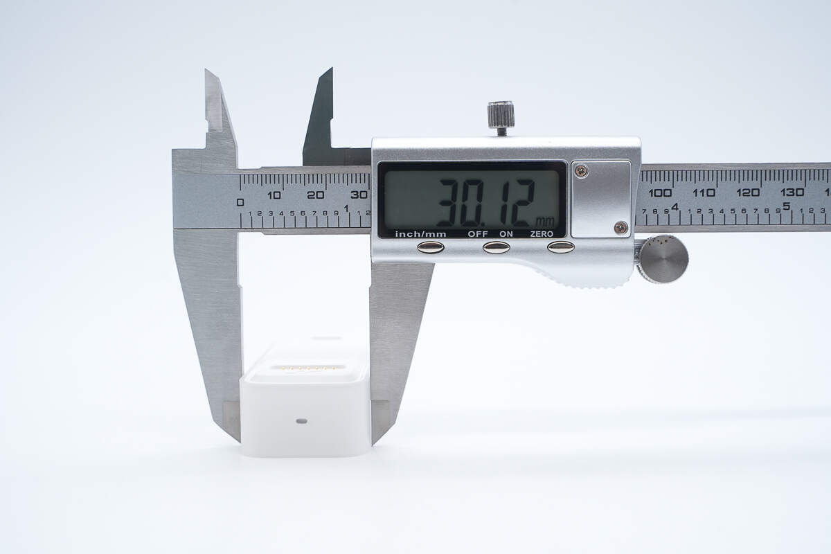
The width is about 30.1 mm (1.19 inches).

The thickness is about 18.5 mm (0.73 inches).
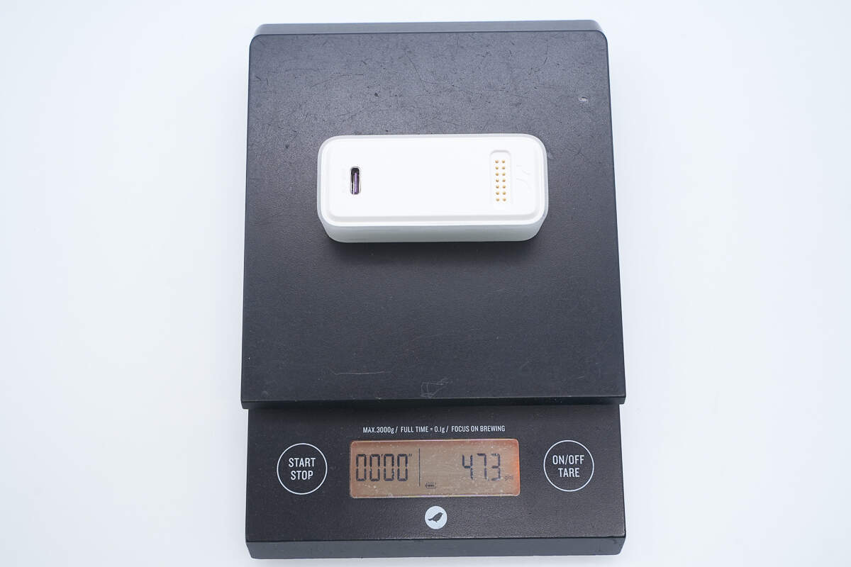
The weight is about 47.3 g (1.67 oz).
The 67W GaN fast charging module’s contacts are also covered with a protective sticker.
Close-up of the contacts.
The side is labeled with "GaN."
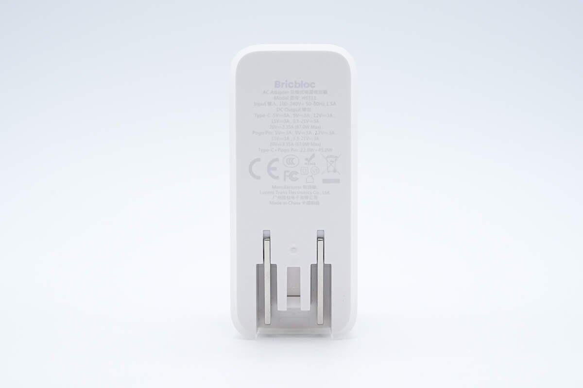
The bottom has specification information and foldable plug pins.
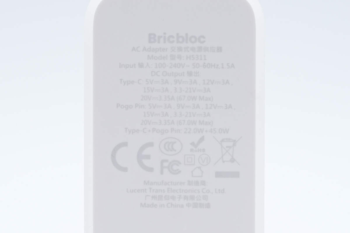
Model: H5311
Input: 100-240V~50/60Hz 1.5A Max
Output:
Type-C: 5V 3A, 9V 3A, 12V 3A, 15V 3A, 3.3-21V 3A, 20V 3.35A (67W Max)
Pogo Pin: 5V 3A, 9V 3A, 12V 3A, 15V 3A, 3.3-21V 3A, 20V 3.35A (67W Max)
Type-C + Pogo Pin: 22W + 45W
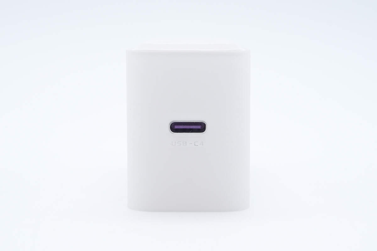
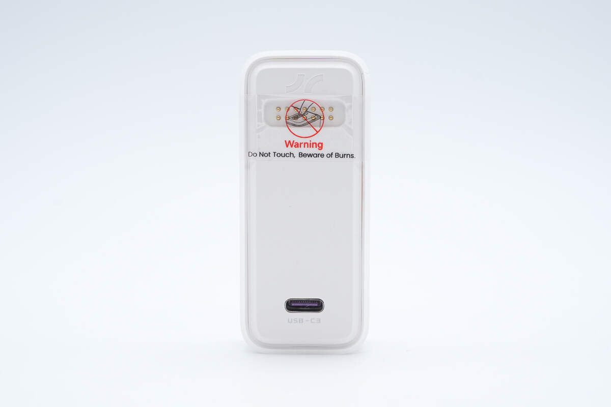
The bottom is equipped with a USB-C female port.
The length is about 70.2 mm (2.76 inches).
The width is about 30.1 mm (1.19 inches).
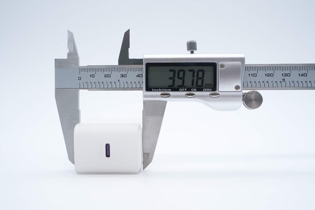
The thickness is about 39.8 mm (1.57 inches).
The weight is about 107 g (3.77 oz).
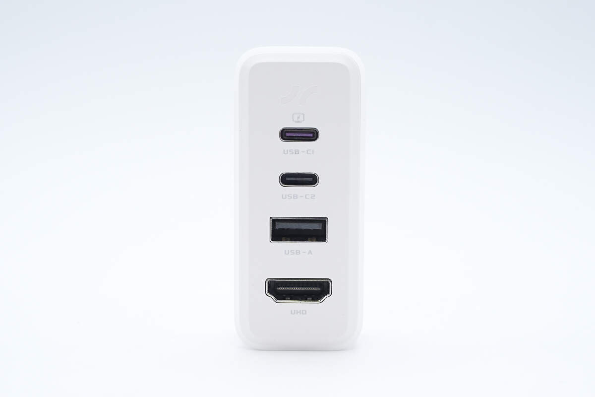
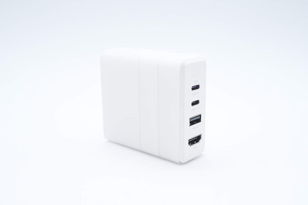
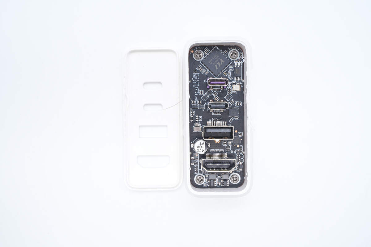
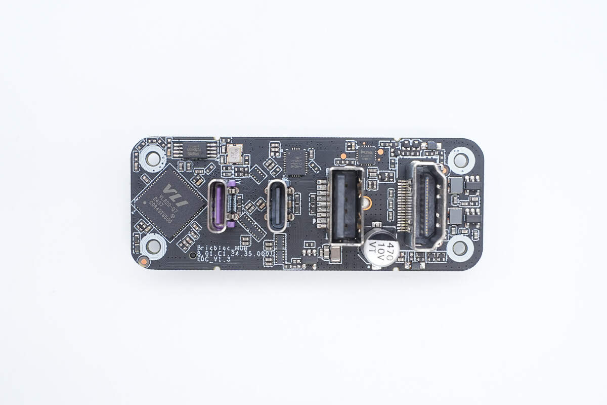
The docking station module has two USB-C ports, one USB-A port, and one HDMI port.
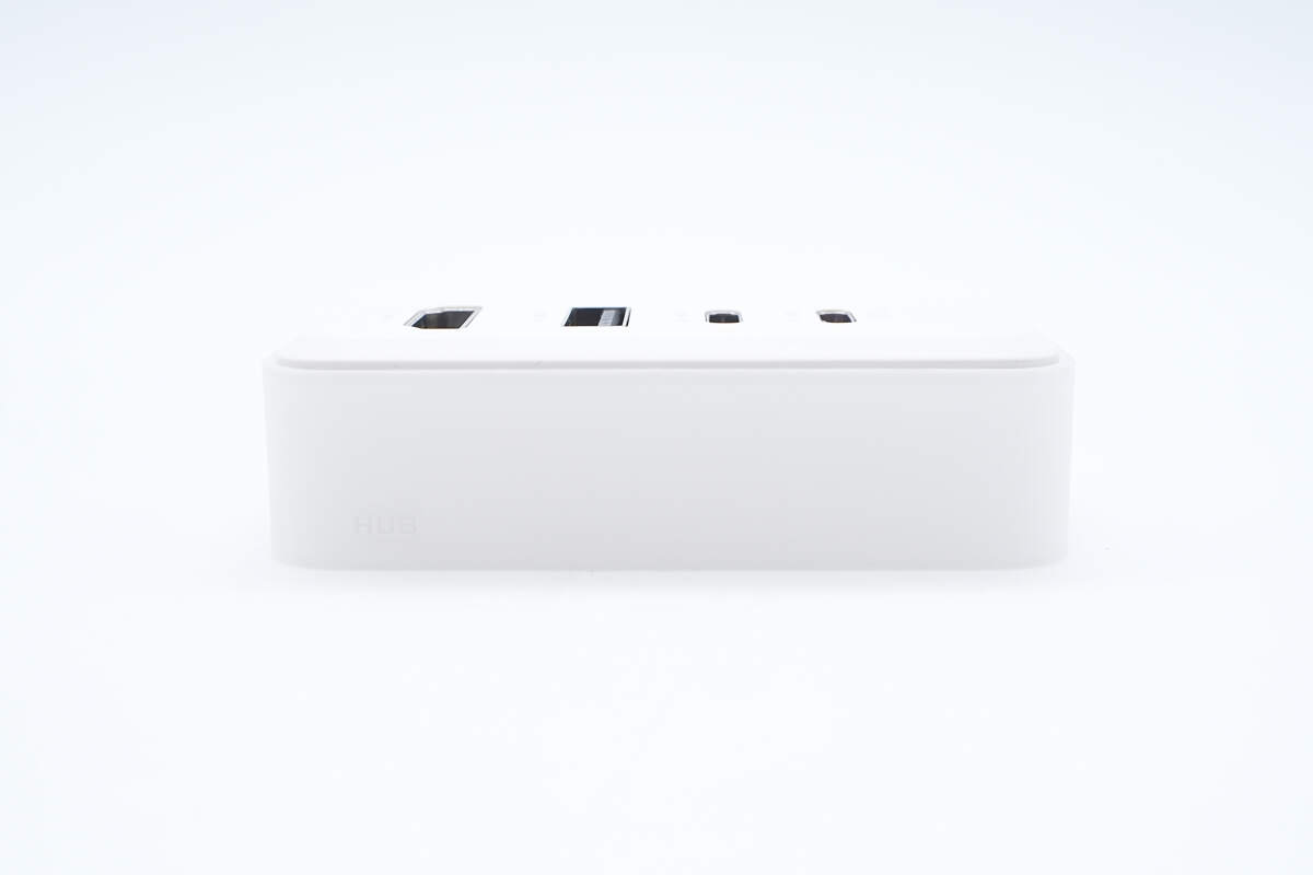
The side is printed with "HUB."
Inside, there are Pogo Pin contacts and specification information.
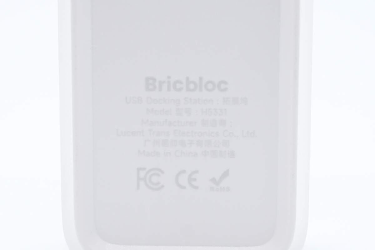
Model H5331.
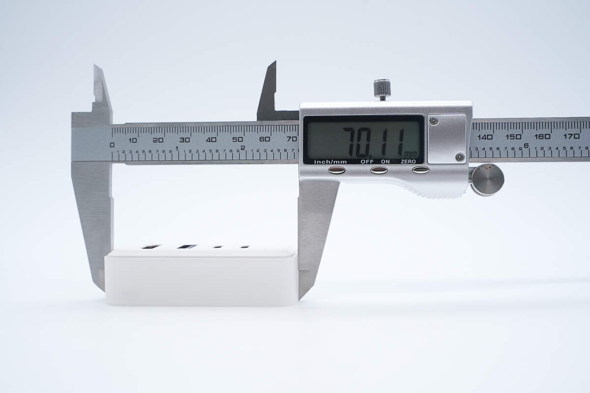
The length is about 70.1 mm (2.76 inches).
The width is about 30.1 mm (1.19 inches).
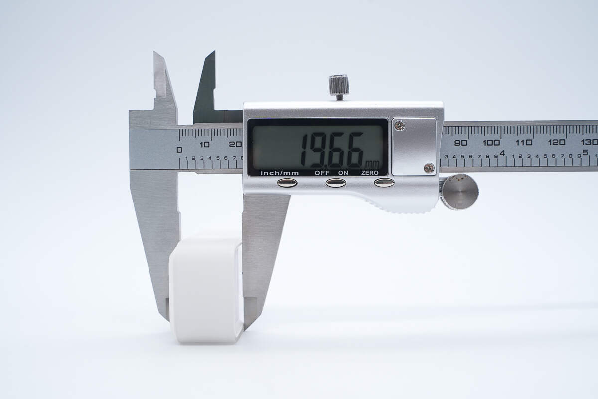
The thickness is about 19.7 mm (0.78 inches).
The weight is about 36 g (1.27 oz).
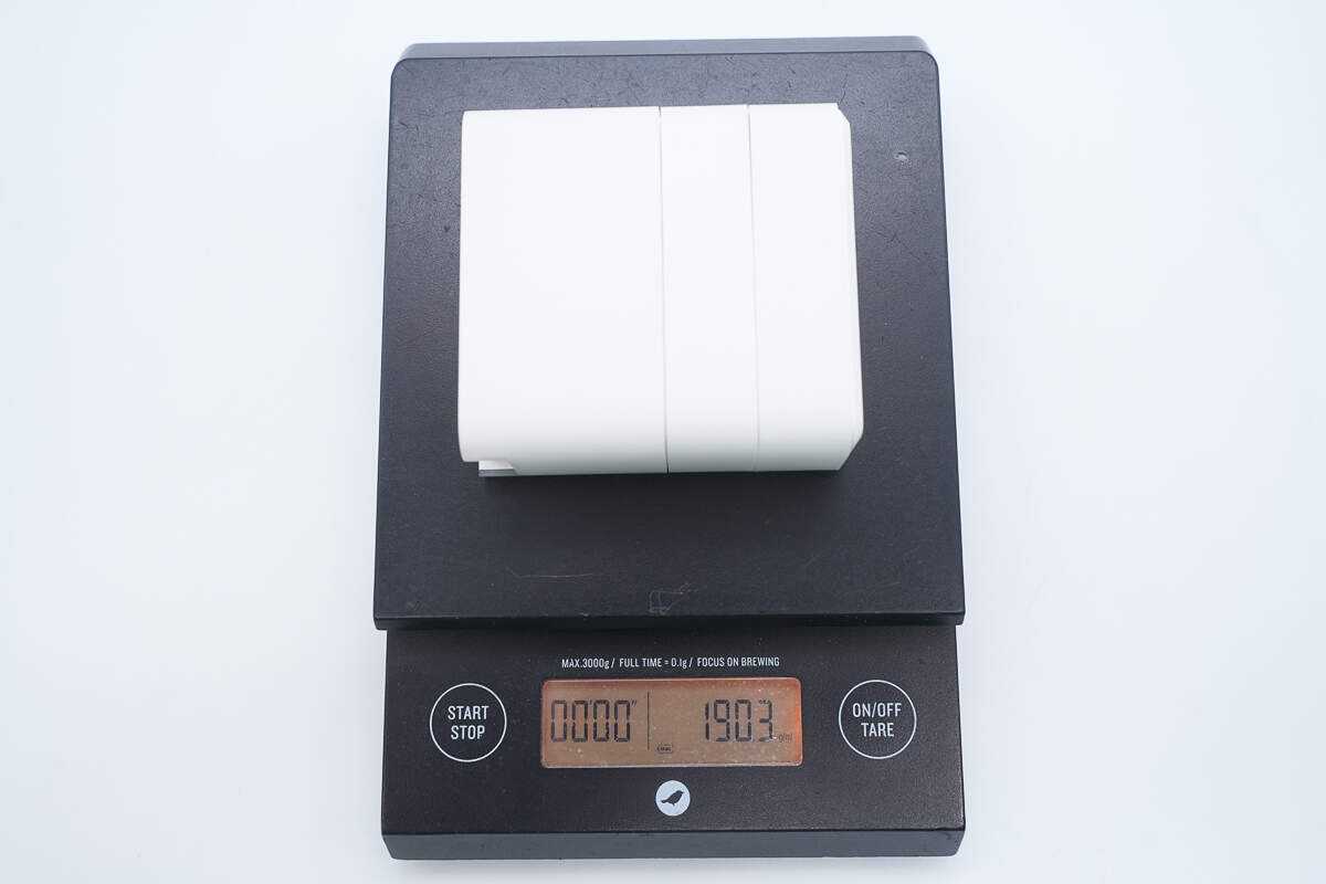
An overview of the three modules assembled together.
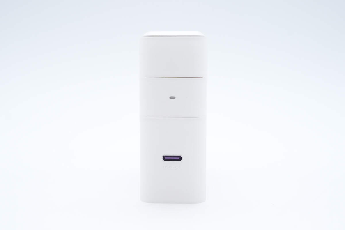
The side has a USB-C port and an LED indicator light.
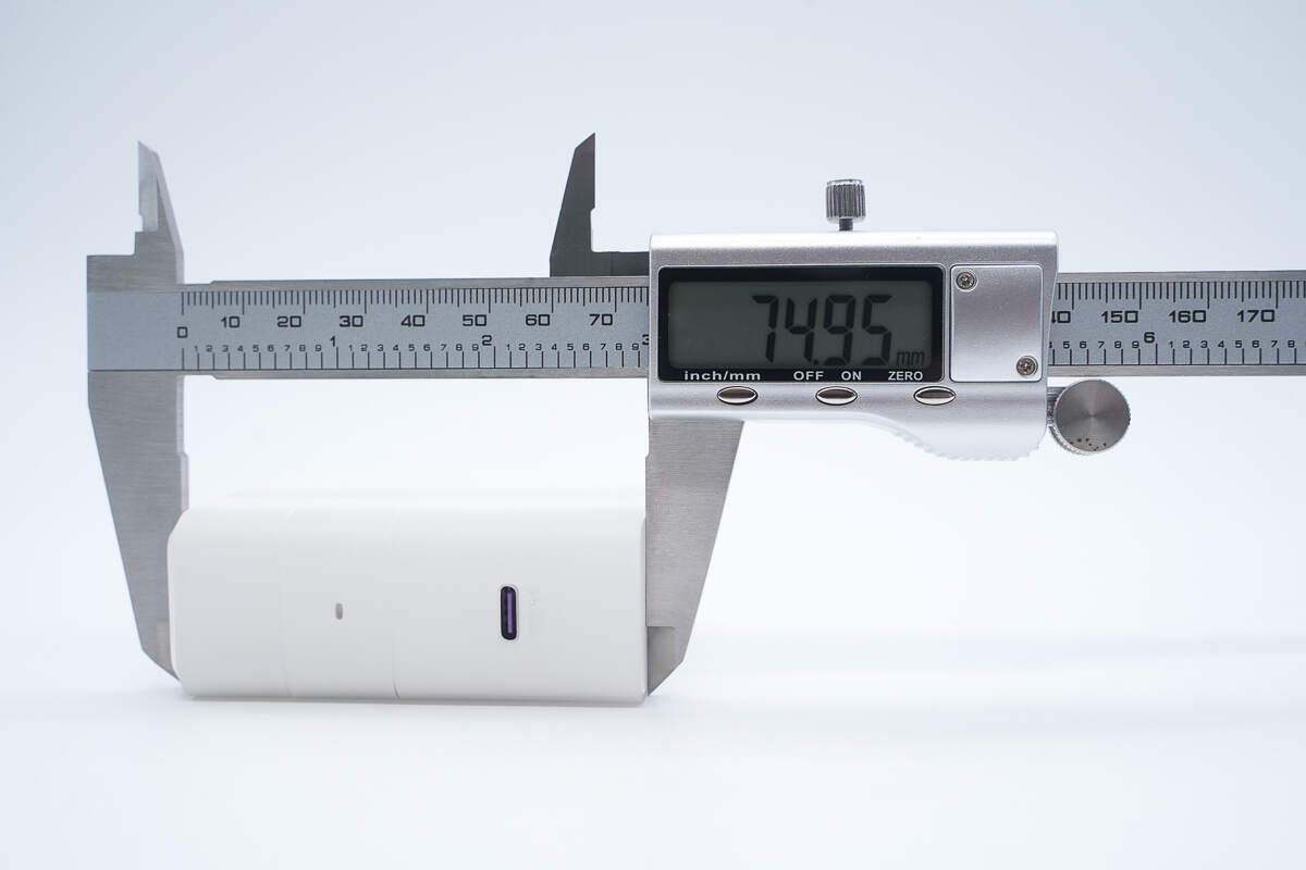
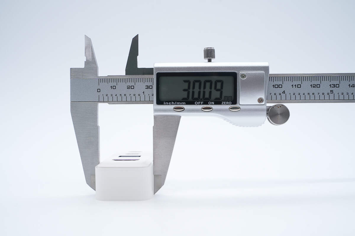
The height is about 75 mm (2.95 inches).
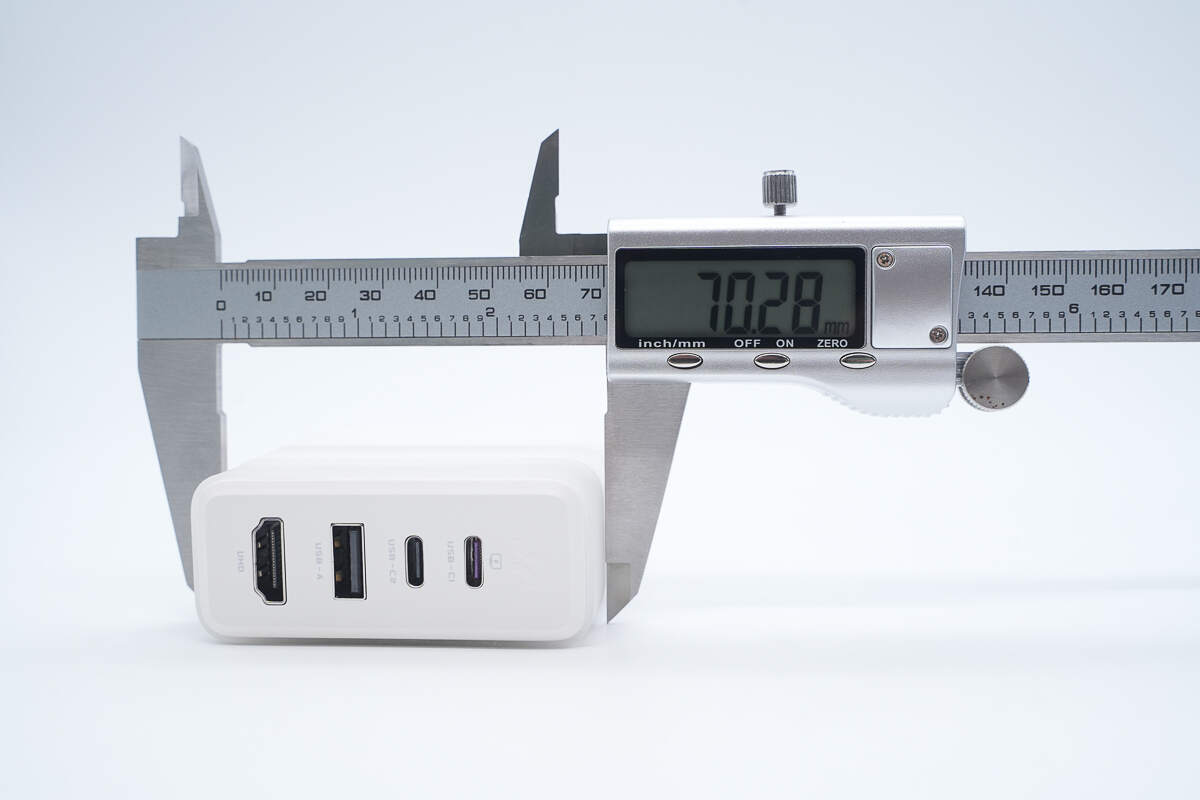
The width is about 70.3 mm (2.77 inches).
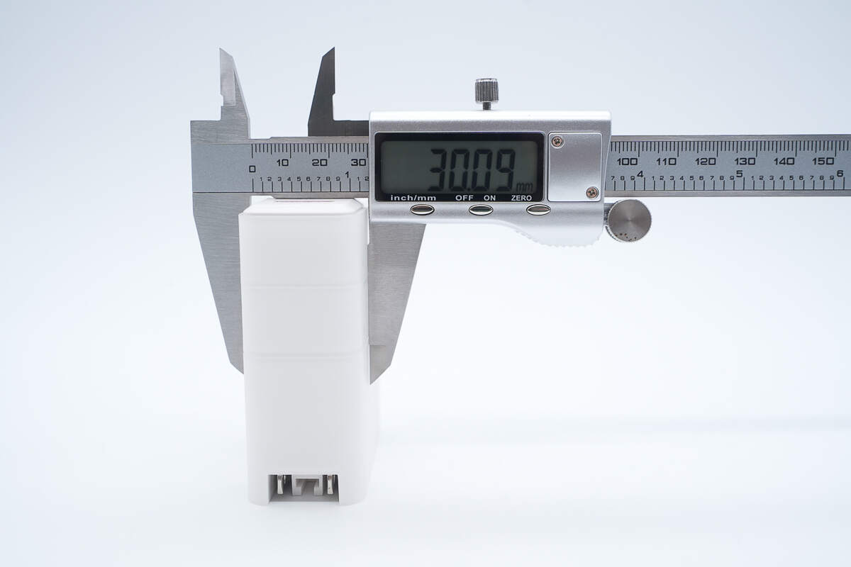
The thickness is about 30.1 mm (1.19 inches).

That's how big it is in the hand.
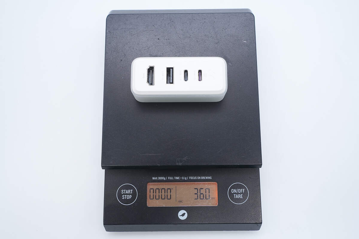
The weight is about 190.3 g (6.71 oz).
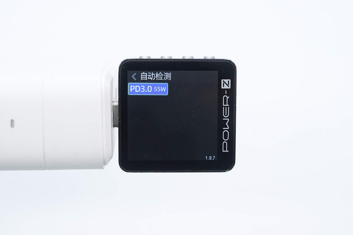
ChargerLAB POWER-Z KM003C shows that the USB-C1 supports PD3.0 charging protocol.
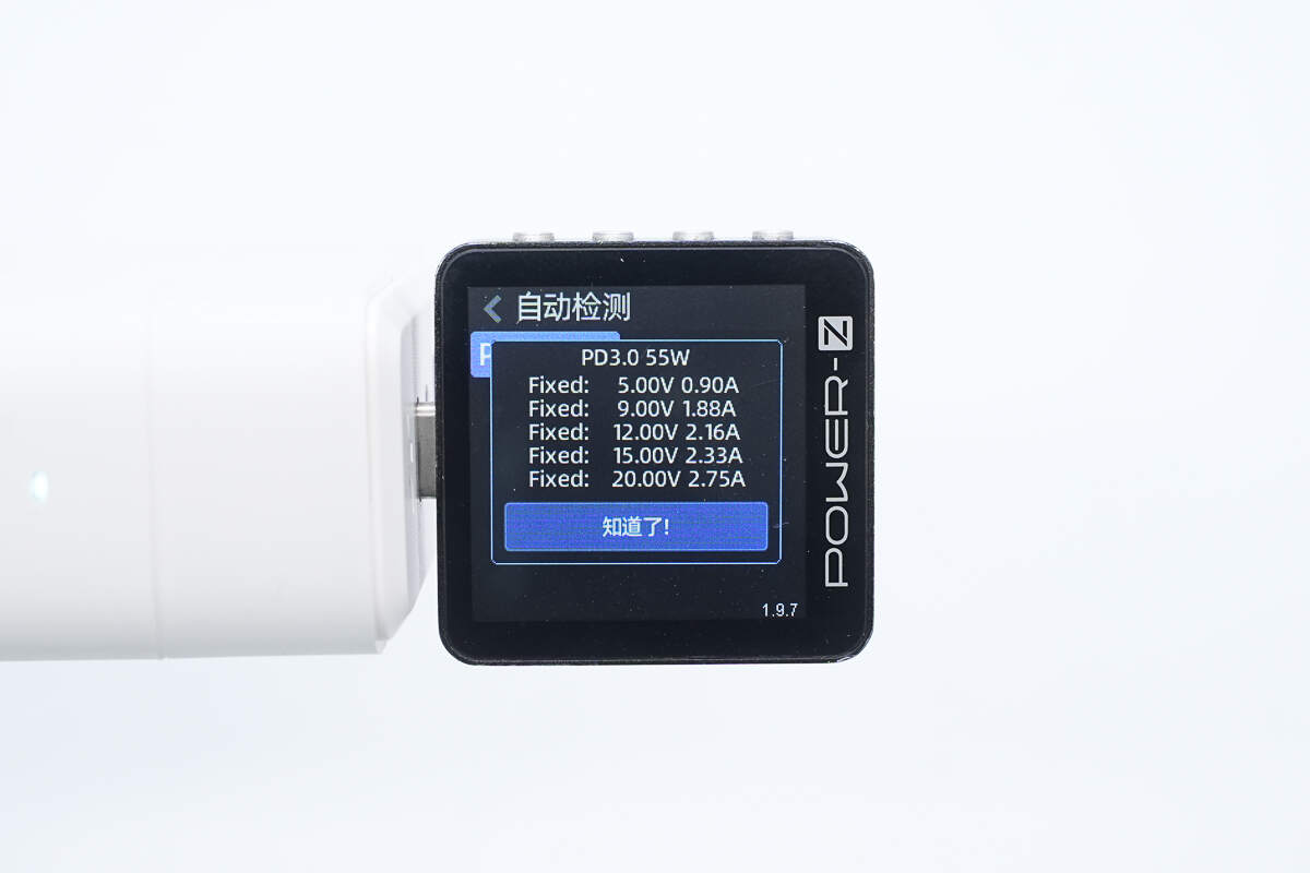
And it has five fixed PDOs of 5V0.9A, 9V1.88A, 12V2.16A, 15V2.33A, and 20V2.75A.
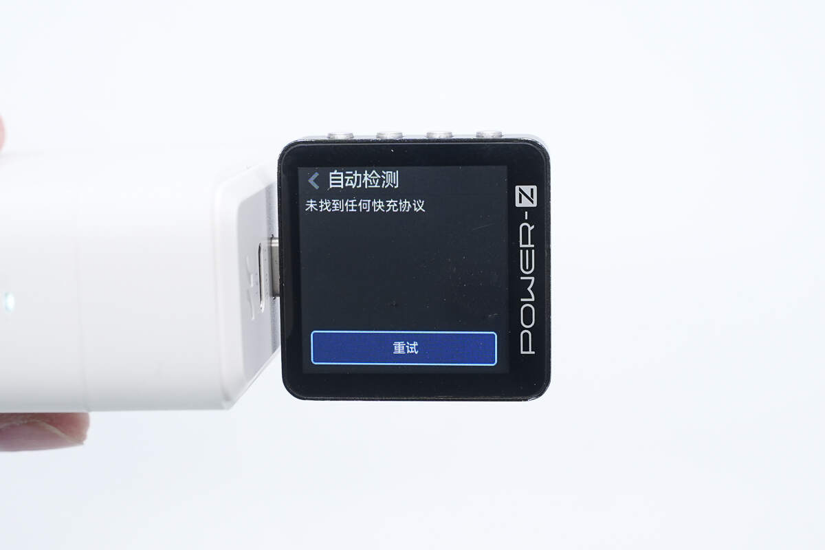
The USB-C2 port does not support fast charging.
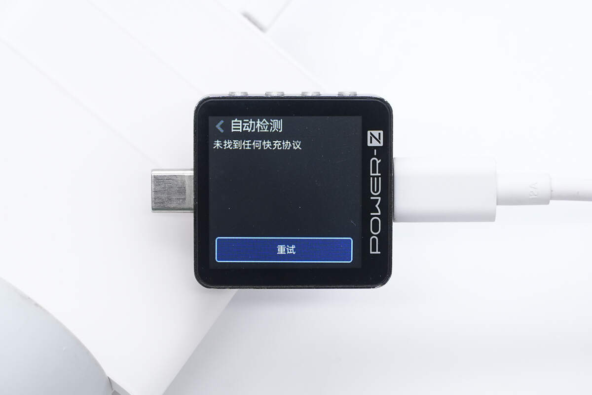
The USB-A port does not support fast charging.

The USB-C port on the side of the fast charging module supports QC3, FCP, SCP, AFC, PD3.0, DCP, SAM 2A, and Apple 2.4A charging protocols.
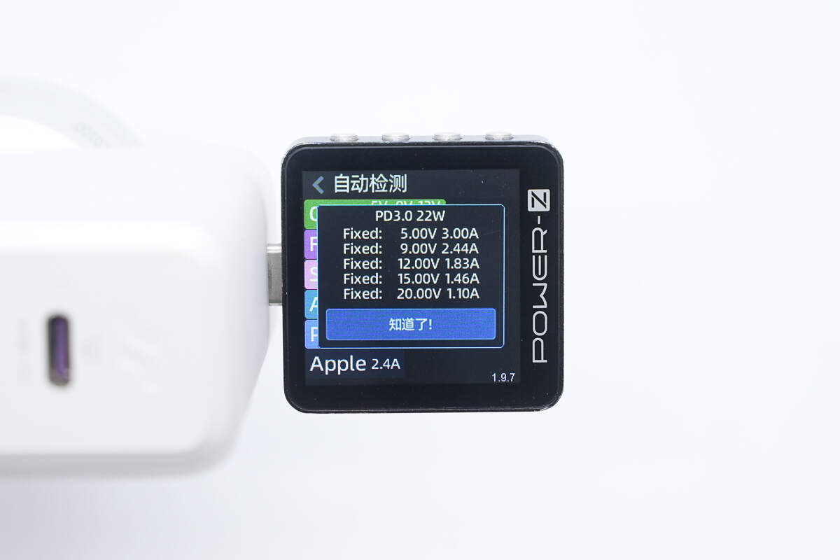
And it has five fixed PDOs of 5V3A, 9V2.44A, 12V1.83A, 15V1.46A, and 20V1.1A.
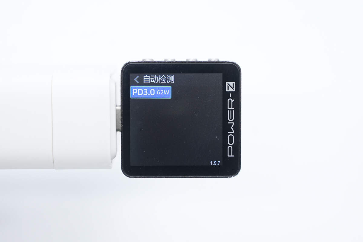
The USB-C port on the SSD module supports the PD3.0 fast charging protocol.
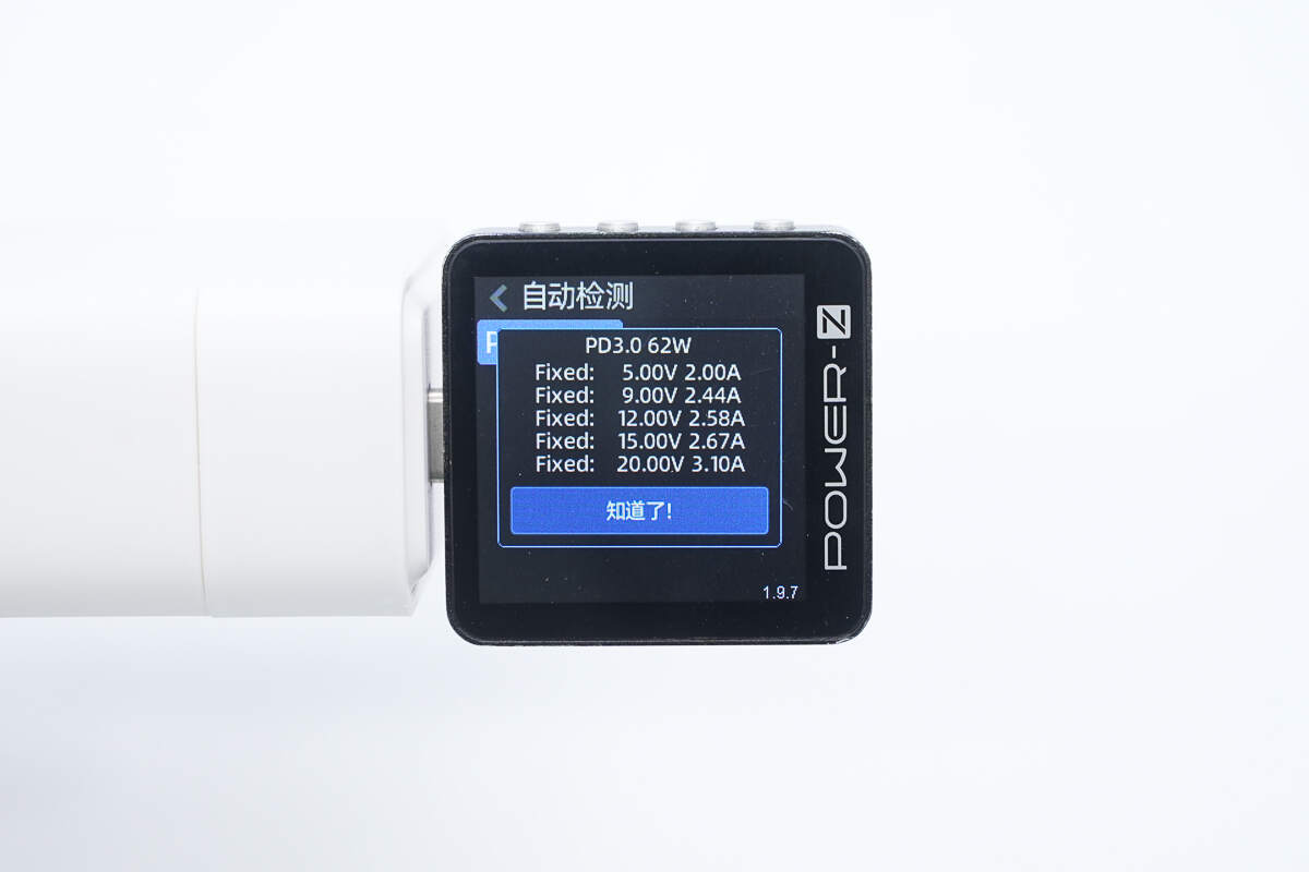
And it has five fixed PDOs of 5V2A, 9V2.44A, 12V2.58A, 15V2.67A, and 20V3.1A.
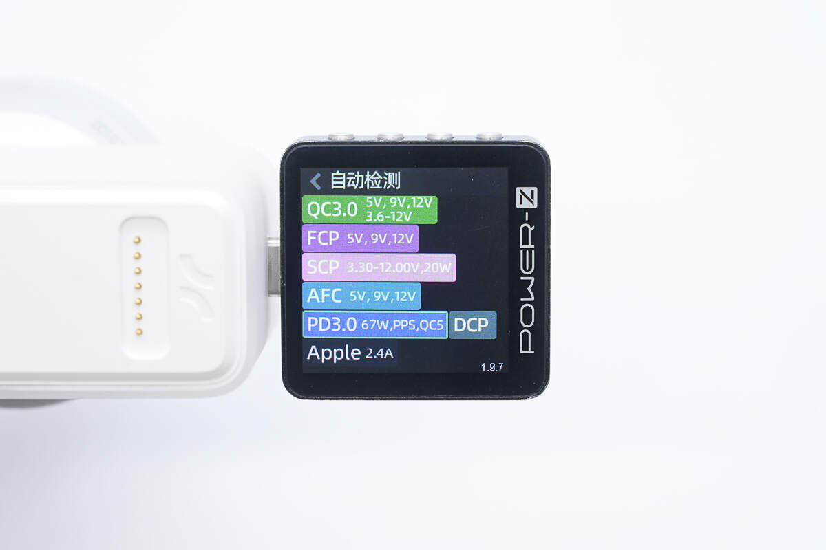
The USB-C port on the side of the fast charging module supports QC3/5, FCP, SCP, AFC, PD3.0, PPS, DCP, SAM 2A, and Apple 2.4A charging protocols.
And it has five fixed PDOs of 5V2A, 9V2.44A, 12V2.58A, 15V2.67A, and 20V3.1A.
Teardown
Next, let's take it apart to see its internal components and structure.
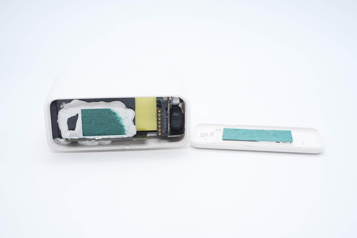
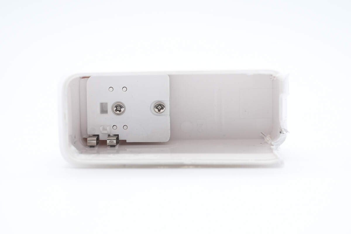
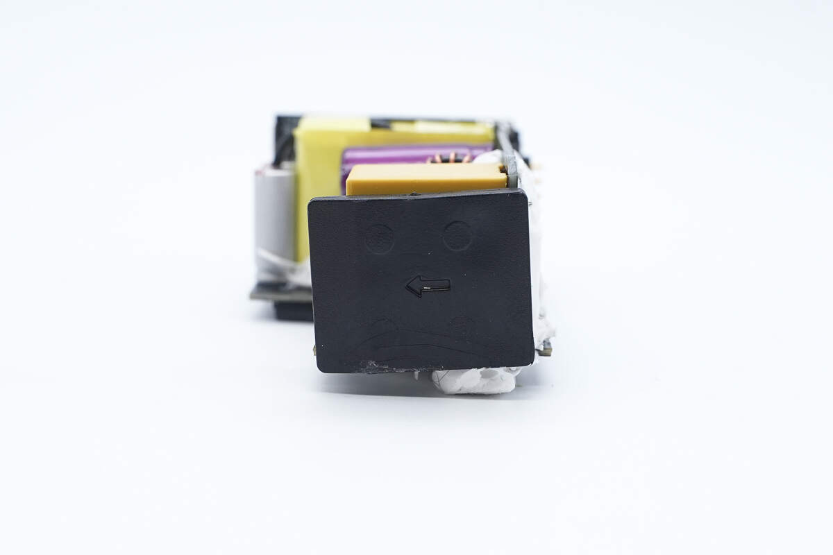
Open the fast charging module’s casing along the seam.
Inside the casing, there are magnets and an insulating kraft paper adhesive.
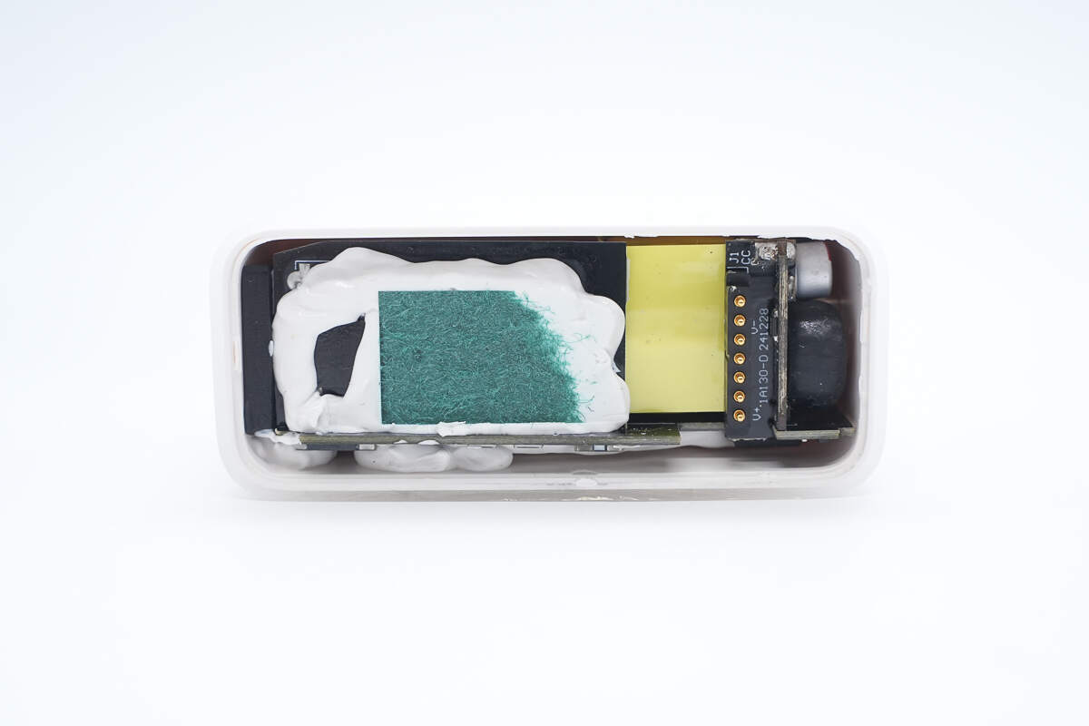
The PCBA module is glued inside the casing.
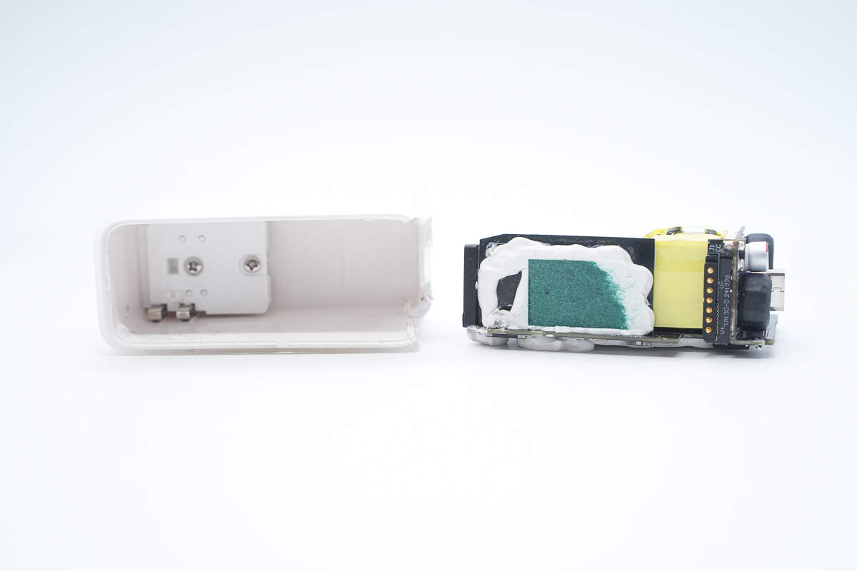
Remove the PCBA module.
The foldable plug pins are connected to the PCBA module through spring clip crimping.
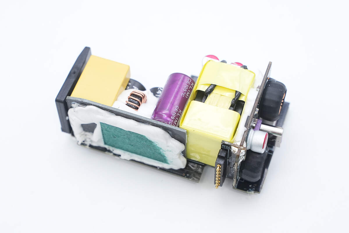
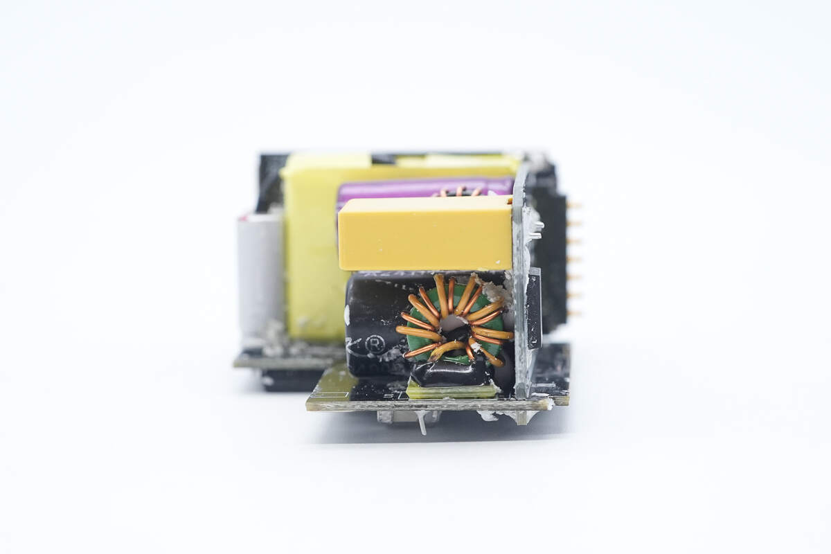
The PCBA module consists of several small PCBs.
The transformer is secured with adhesive for reinforcement.
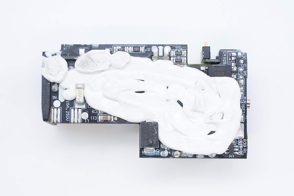
The back of the PCBA module is coated with thermal adhesive to enhance heat dissipation.
The side of the PCBA module is filled with a plastic block.
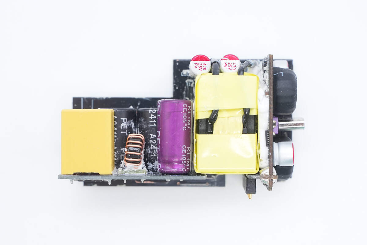
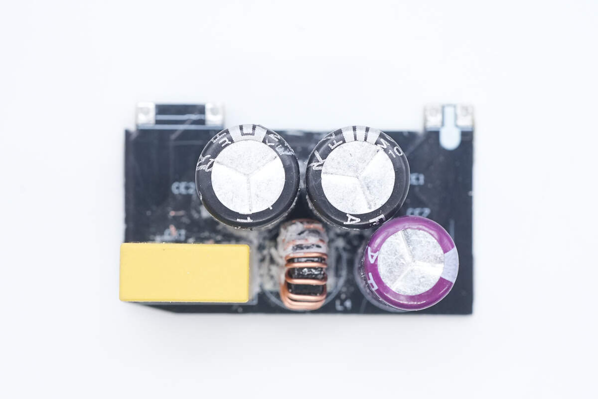
On the front side of the PCBA module, there are a safety X2 capacitor, a common-mode choke, high-voltage filter capacitors, a transformer, solid-state capacitors, and a buck output PCB.
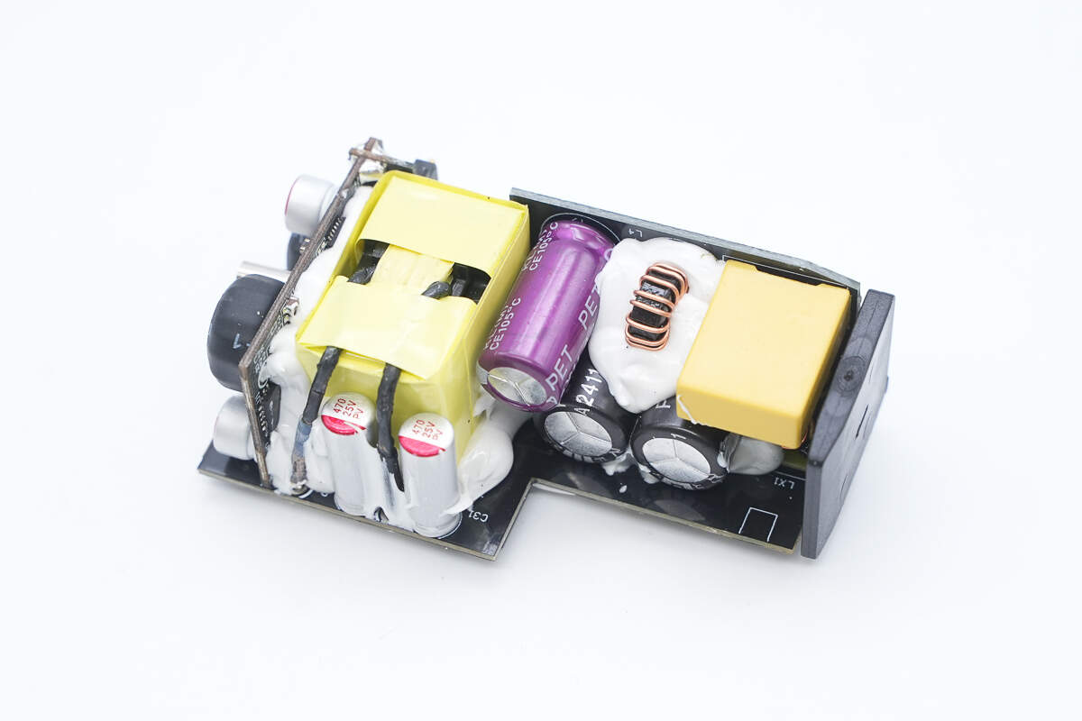
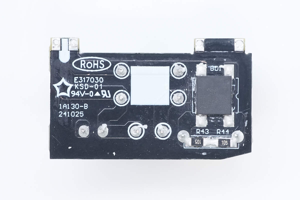
On the back side, there is an integrated GaN chip, an SMD Y capacitor, an optocoupler for feedback, a synchronous rectification controller, and a synchronous rectifier.
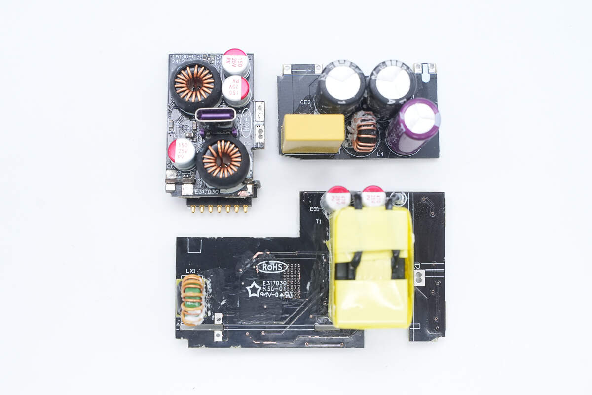
Disassemble the individual small PCBs.
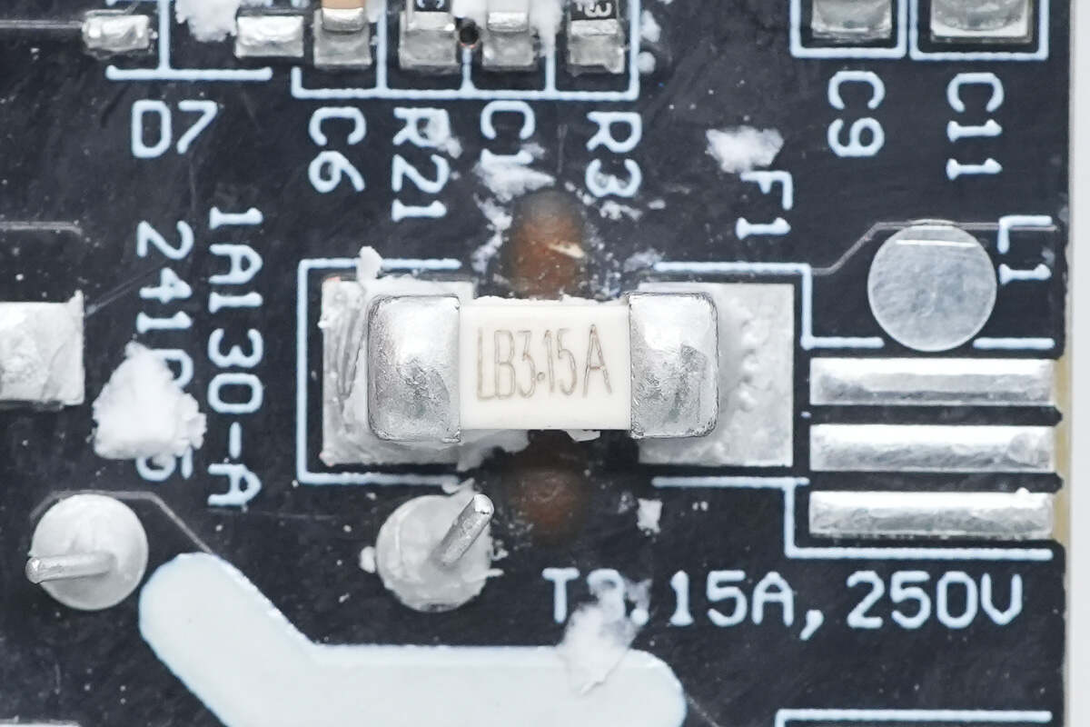
The SMD fuse at the input end is from Lanbao, rated at 3.15A 250V.
The common mode choke is wound with magnet and insulated wires, and it's also insulated with bakelite.
The rectification and filtering of a small PCB is equipped with a safety X2 capacitor, a differential mode inductor, and electrolytic capacitors.
A bridge rectifier is soldered on the back side.
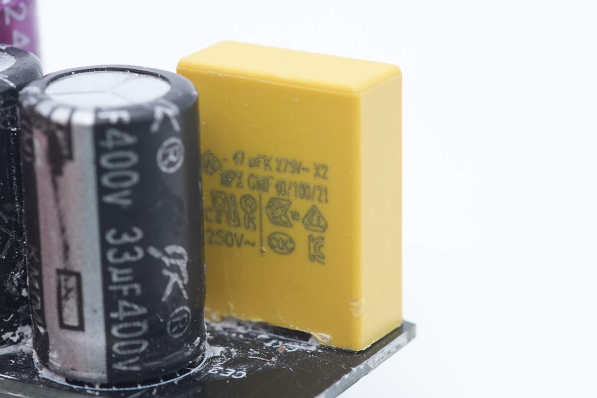
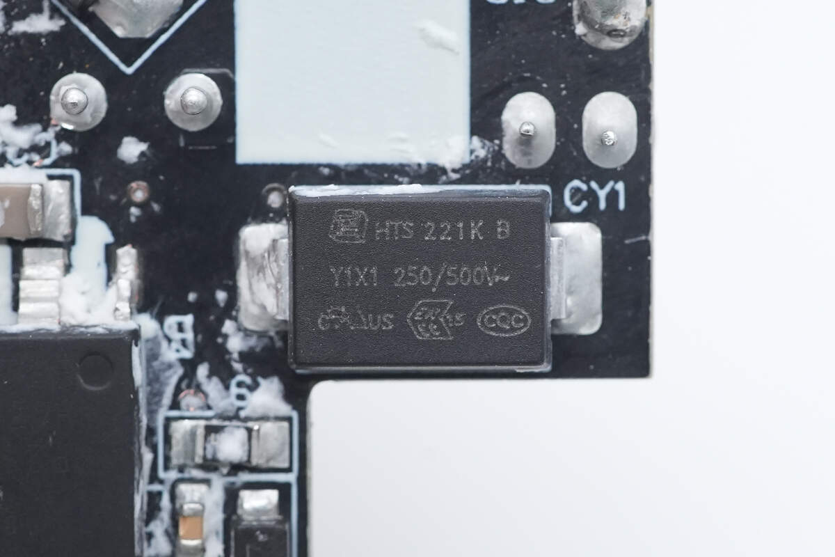
The safety X2 capacitor is rated at 0.47μF.
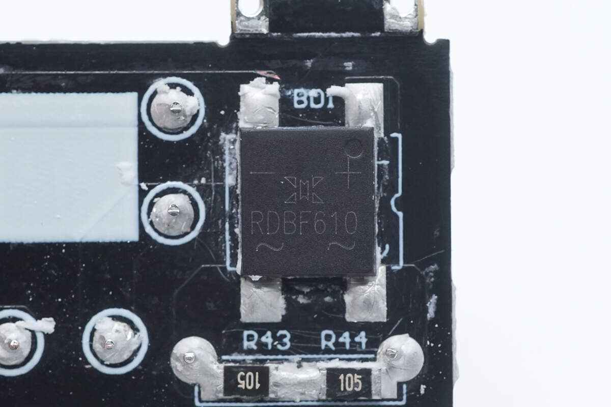
The bridge rectifier is model RDBF610, rated at 6A 1000V, and uses a DBF package.
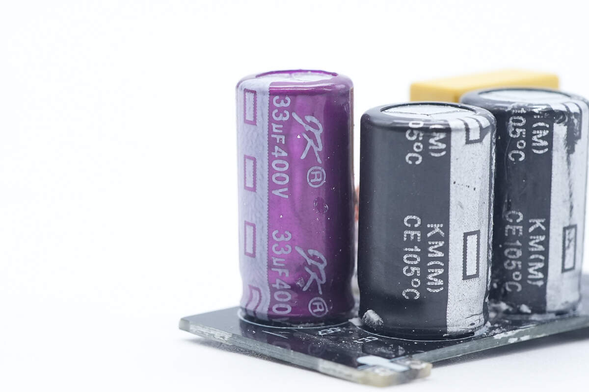
The filter capacitor is from JK, rated at 33μF 400V.
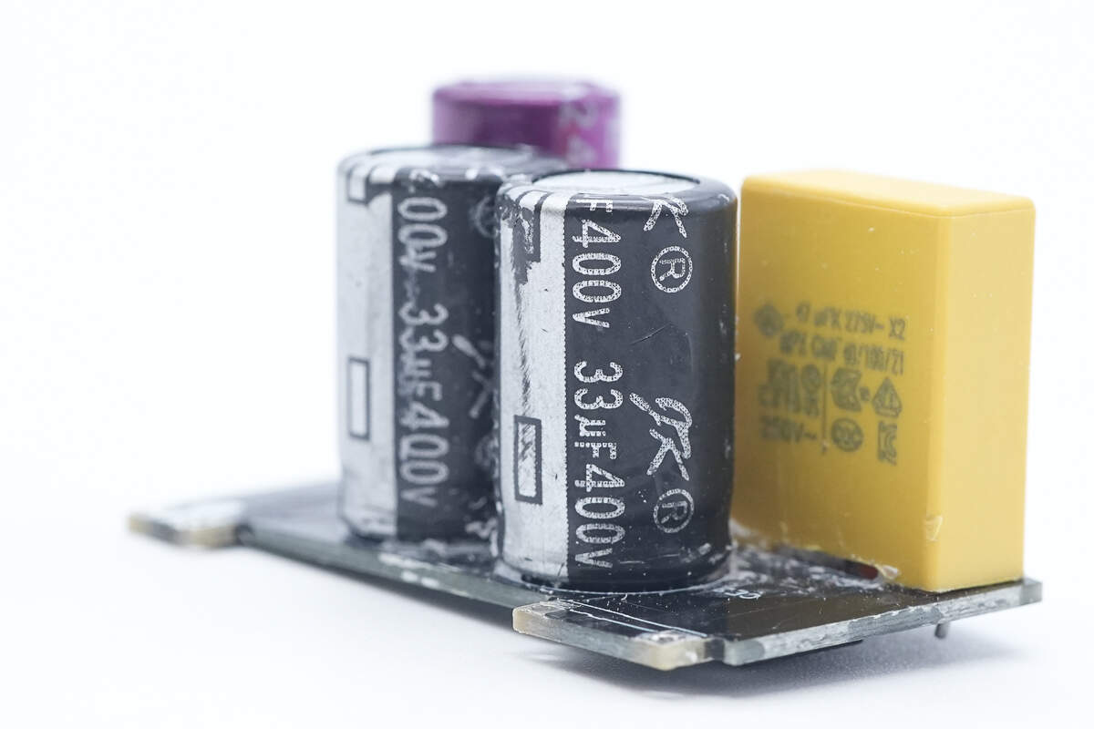
The other two capacitors have the same specifications.
The differential mode inductor is wound with magnet and insulated wires, and it's also insulated with bakelite.
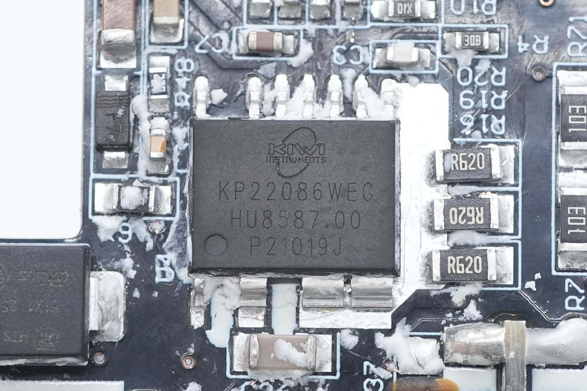
The master control chip is from Kiwi Instruments, model KP22086. It is a high-frequency, high-performance quasi-resonant mode AC-DC power switch integrated with E-GaN technology. It features an integrated high-voltage startup circuit, enabling fast startup and ultra-low operating current, achieving standby power consumption of less than 30mW.
The KP2208X operates at frequencies up to 220kHz and can work fully in quasi-resonant mode across its range. It includes peak current jitter and drive current configuration functions, significantly optimizing system EMI performance. The chip also has a built-in boost power supply circuit, making it well-suited for applications requiring wide output voltage ranges. It uses an ESOP-10W package and supports power applications from 20W to 120W.
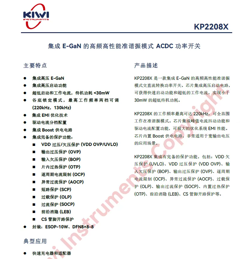
The KP2208X integrates comprehensive protection features, including: VDD under-voltage lockout (UVLO), VDD over-voltage protection (VDD OVP), input under-voltage protection (BOP), output over-voltage protection (OVP), cycle-by-cycle over-current limit (OCP), abnormal over-current protection (AOCP), overload protection (OLP), output short-circuit protection (SOCP), built-in over-temperature protection (OTP), leading-edge blanking (LEB), and open-circuit protection for the CS pin.
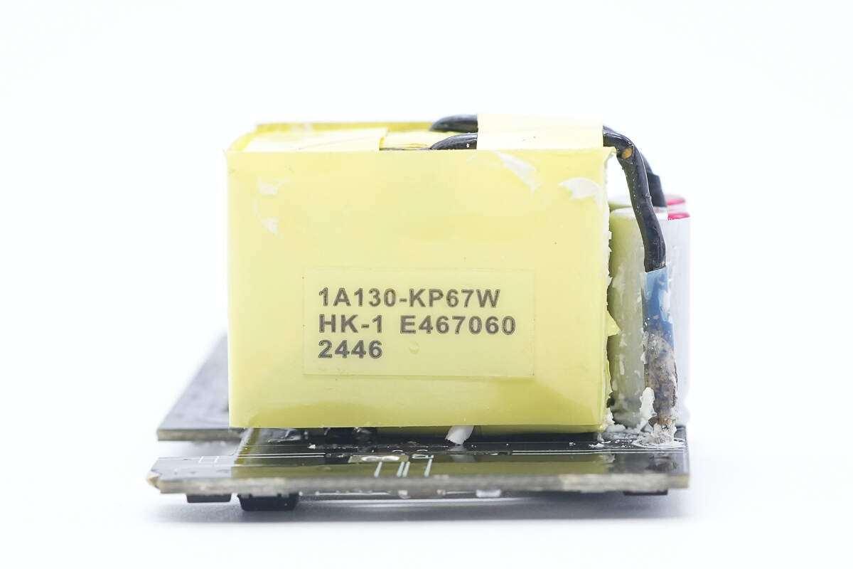
The transformer is insulated with tape wrapping.
Close-up of the SMD Y capacitor.
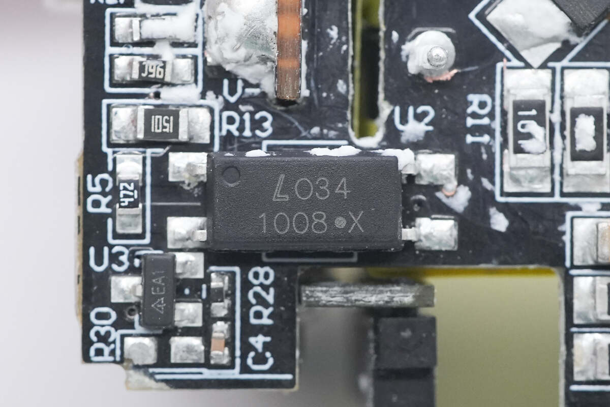
The LITEON LTV1008 optocoupler is used for output voltage feedback.
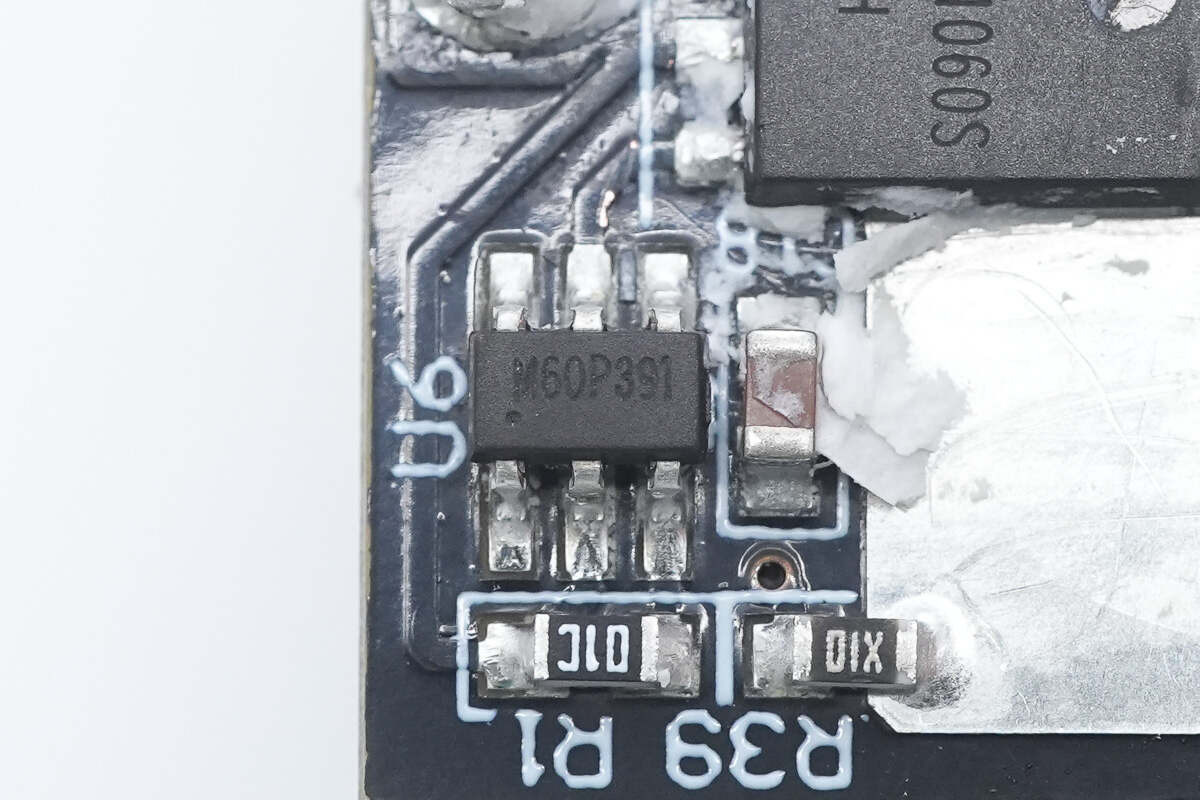
The synchronous rectifier controller marked with M60 is from Kiwi Instruments, model KP4060. It supports DCM, CCM, and QR operating modes, as well as active clamp flyback topology. It operates at a frequency of up to 600kHz and integrates high-voltage detection and high-voltage power supply circuits. The controller features intelligent dual LDOs, eliminating the need for auxiliary winding power supply, and supports synchronous rectification operation during output short circuits. It comes in a space-saving SOT23-6 package.
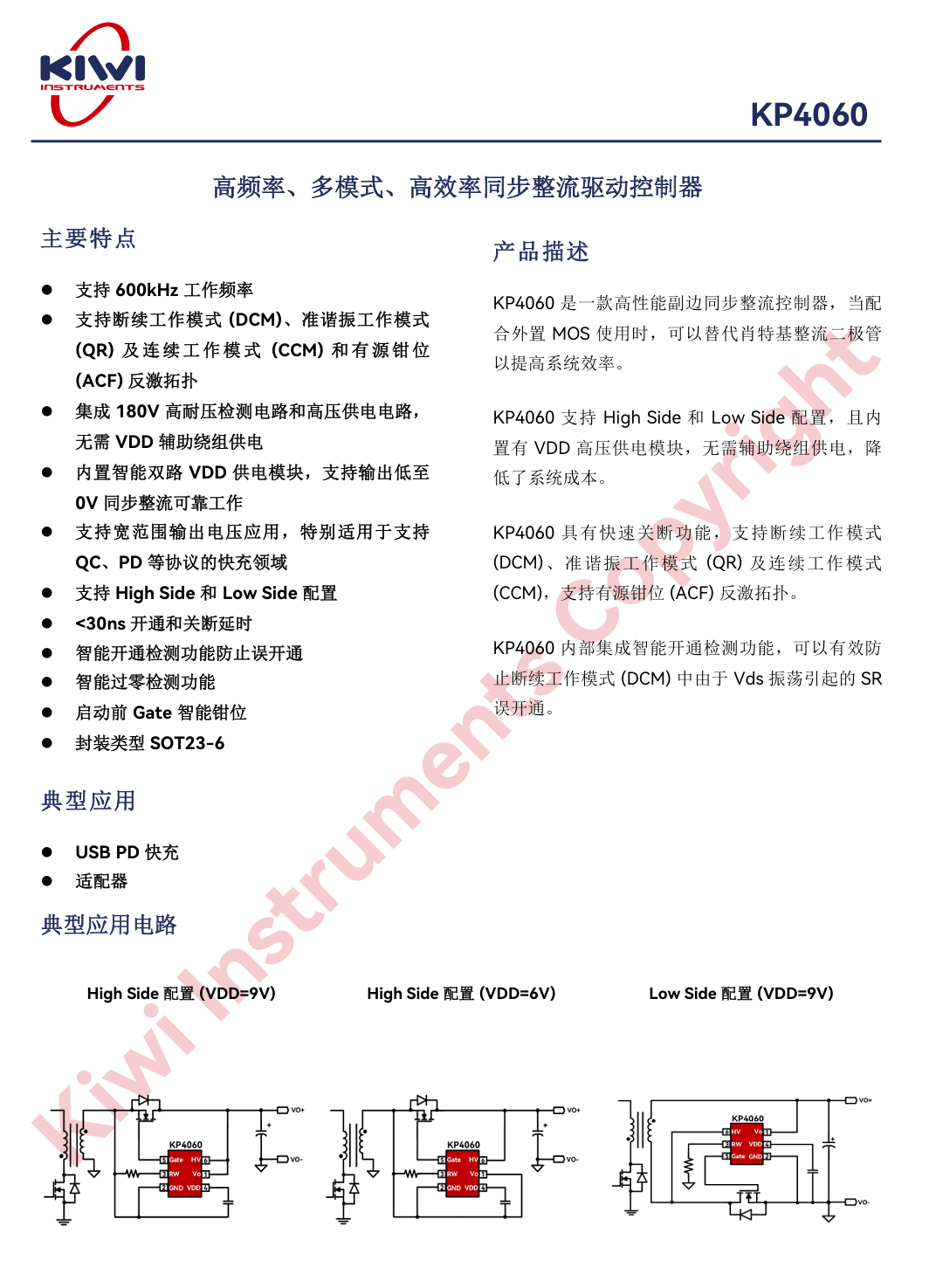
The KP4060 supports a wide range of output voltage applications and is especially suitable for fast charging fields that support protocols such as QC and PD. It supports both high-side and low-side configurations. With turn-on and turn-off delays of less than 30ns, it features gate drive clamping technology to prevent false triggering caused by parasitic coupling. The controller also incorporates patented intelligent current zero-crossing shutdown and intelligent turn-on detection technologies to prevent false activation, ensuring safe operation.
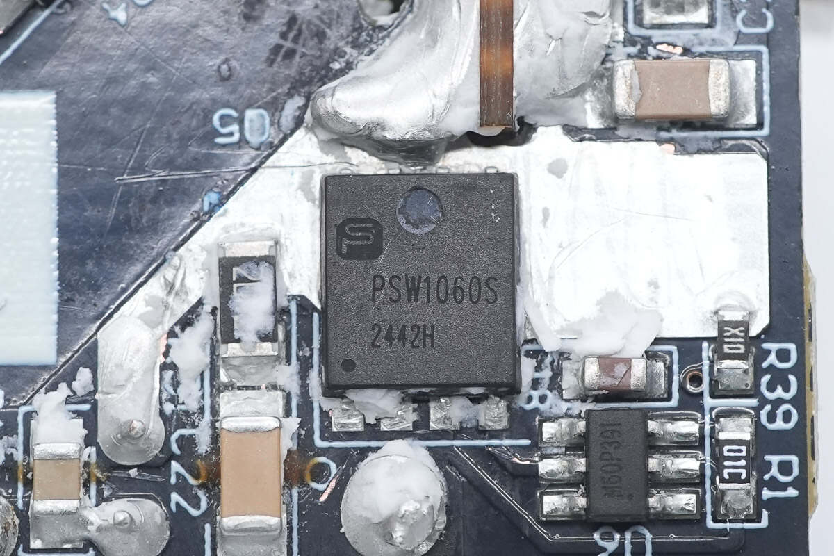
The synchronous rectifier marked with PSW1060S uses a DFN 5×6 package.
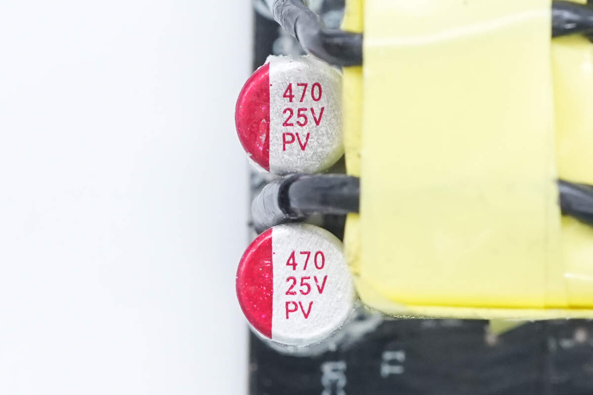
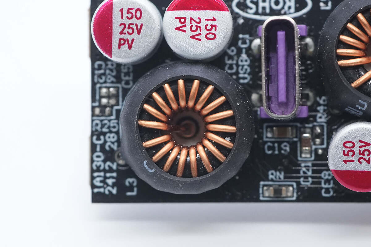
The filter capacitors are rated at 470μF 25V, connected in parallel.
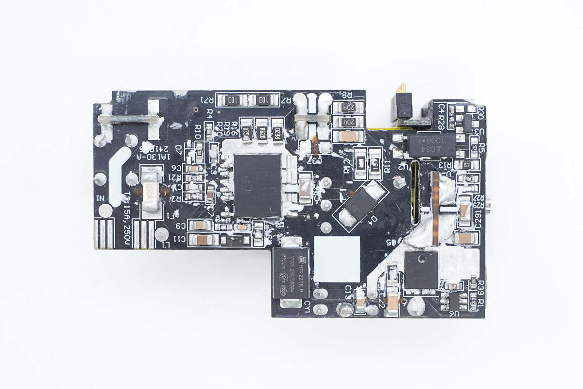
There is a buck converter PCB at the output end.
Remove the buck converter PCB. On the front side, there are two buck inductors, three filter capacitors, and a USB-C socket.
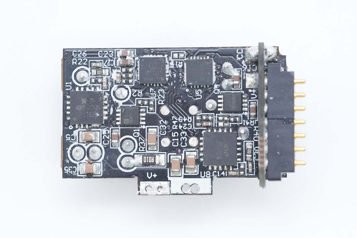
On the back side, there are protocol chips, synchronous buck converters, and VBUS MOSFETs.
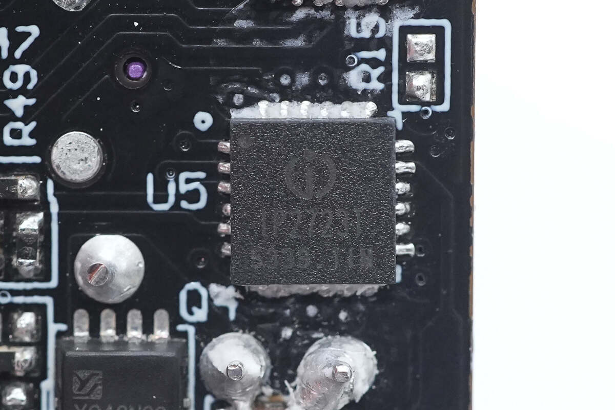
The protocol chip used is the Injoinic IP2723T. This chip has been certified by the USB-IF association for PD3.0 PPS, with TID: 3135. It is a fast charging protocol IC integrated with multiple protocols, designed for USB output ports. It supports a variety of fast charging protocols, including USB Type-C DFP, PD2.0/3.0, PPS, HVDCP, QC4, QC4+, QC3.0/2.0, FCP, SCP, AFC, MTK PE+ 2.0/1.1, Apple 2.4A, BC1.2, and Samsung 2.0A.
It provides a complete Type-C solution for unidirectional output applications such as adapters and car chargers. Additionally, the IP2723T features high integration and rich functionality, requiring very few external components during application, effectively reducing overall solution size and lowering BOM cost.
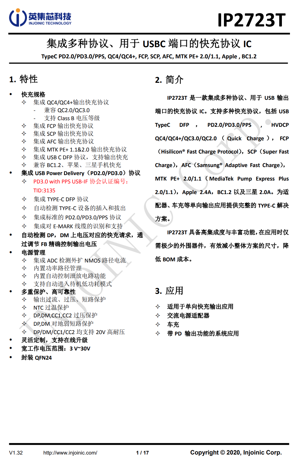
Here is the information about Injoinic IP2723T.
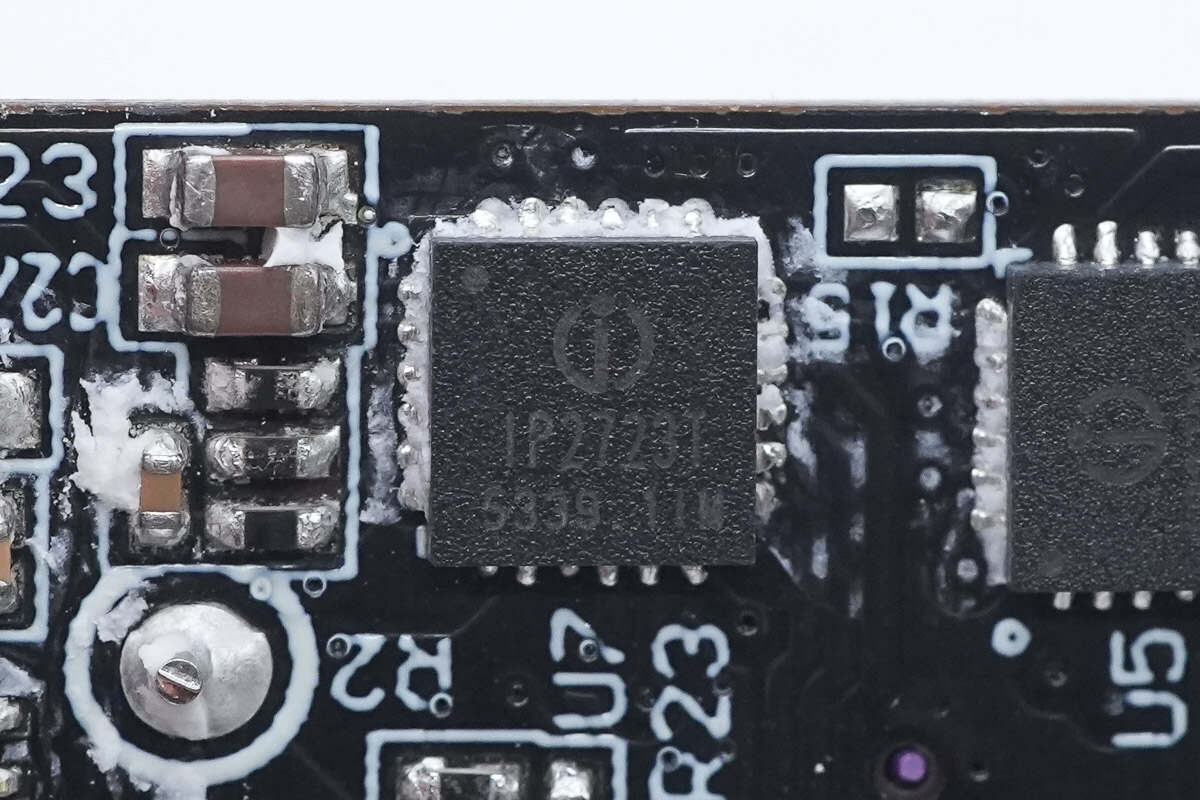
The other protocol chip has the same model.
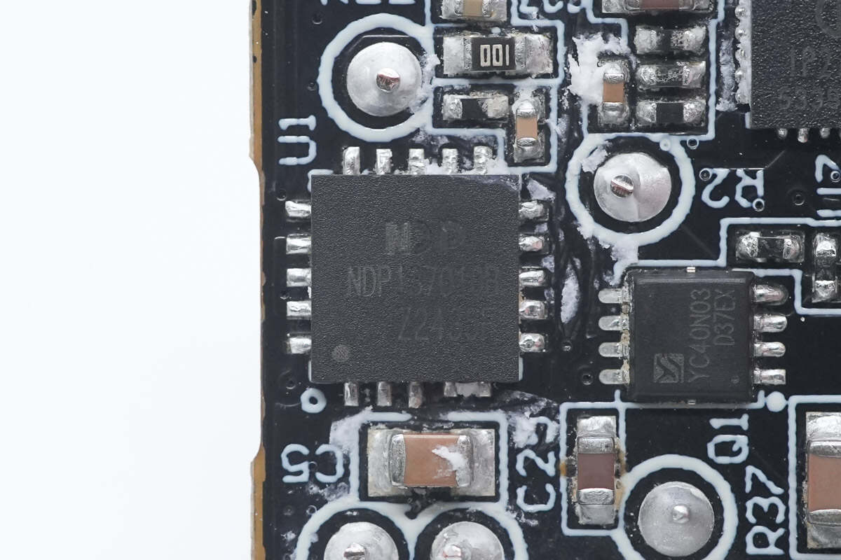
The synchronous buck chip is from NDP, model NDP13701QB. It supports an input voltage range of 7–30V and an output current of 7A. It integrates MOSFETs internally, supports dual constant voltage and constant current control, features built-in loop compensation, and comes in a QFN 5×5 package.
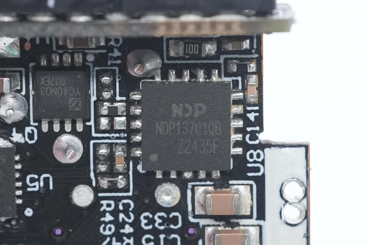
The other synchronous buck chip has the same model.
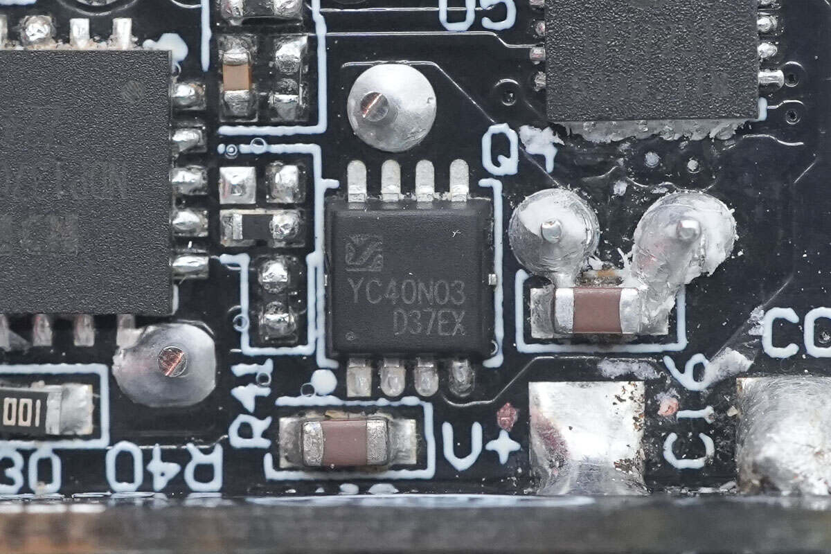
The VBUS MOSFET is from Youcrystal, model YC40N03CDE. It is an NMOS with a voltage rating of 30V and an on-resistance of 9mΩ, packaged in a DFN 3.3×3.3-8 package.
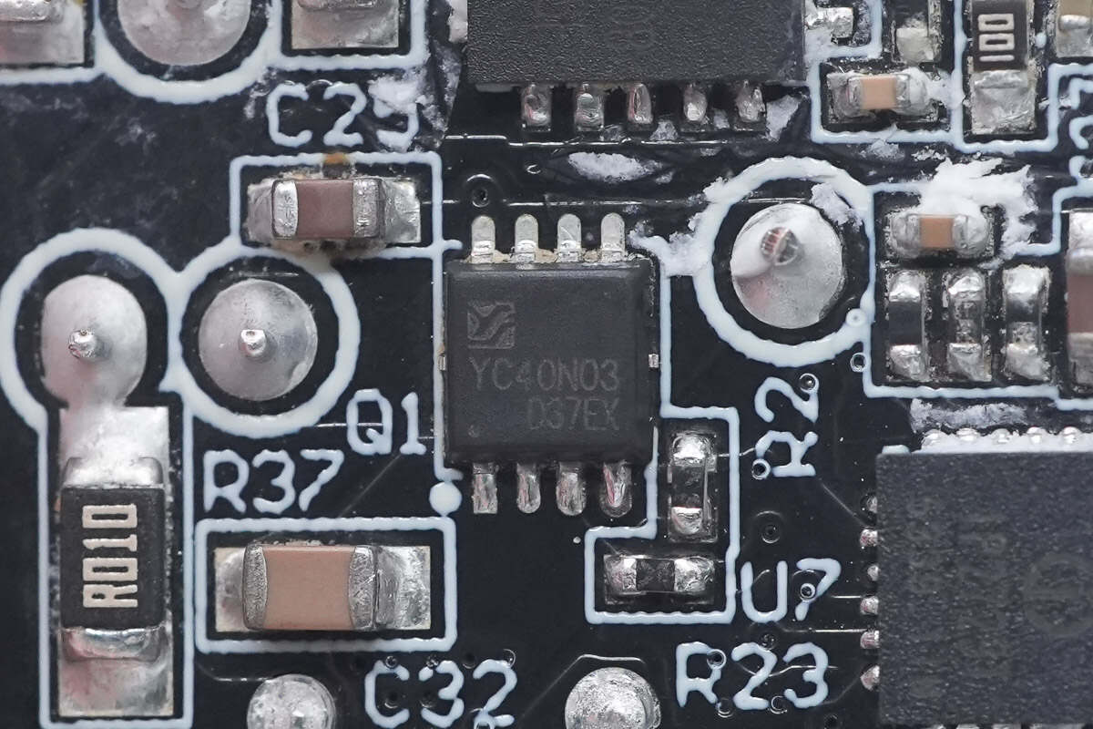
The other VBUS MOSFET is the same model.
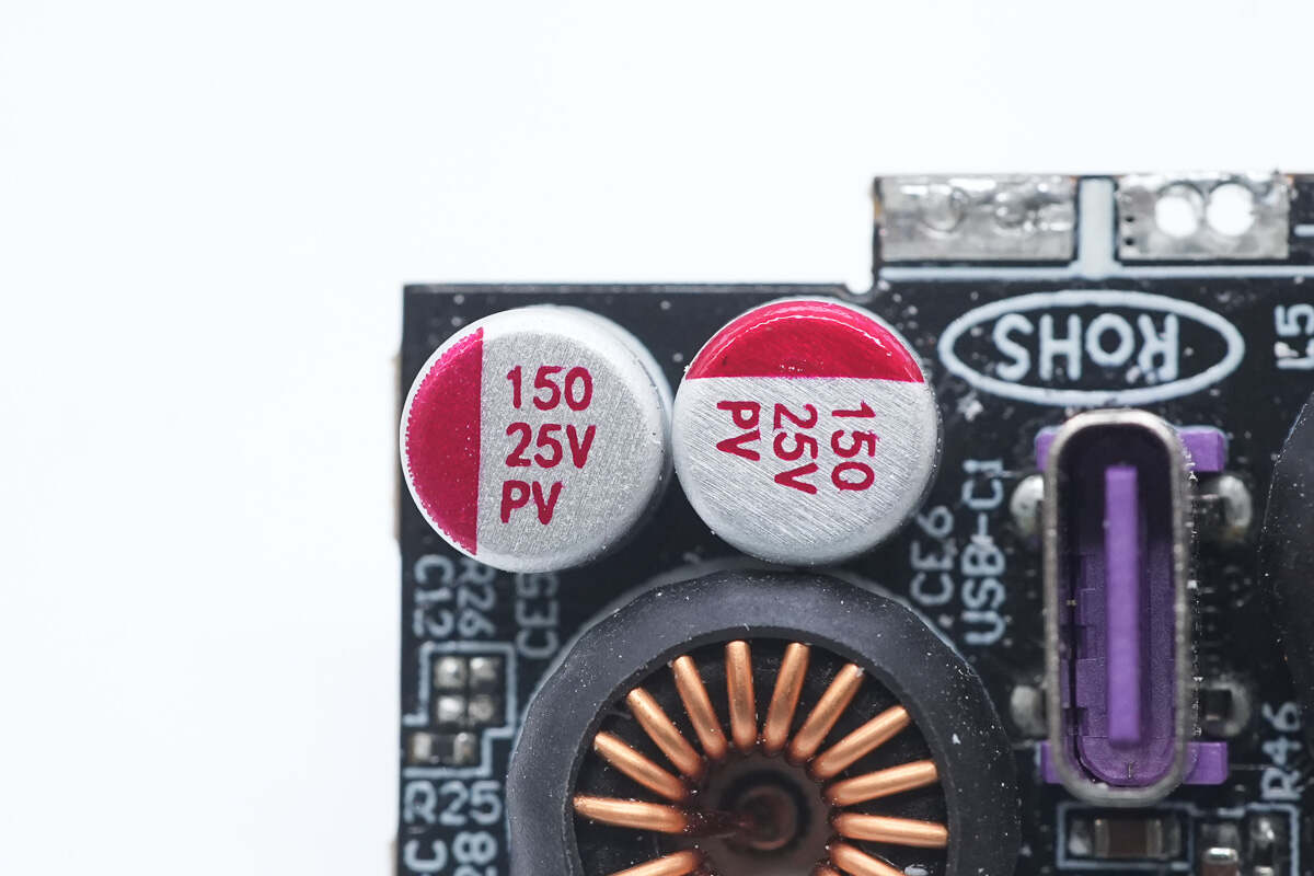
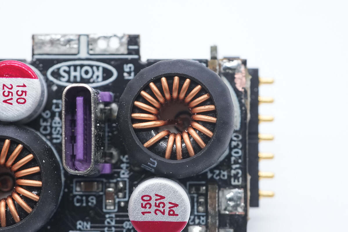
The capacitors are rated at 150μF 25V.
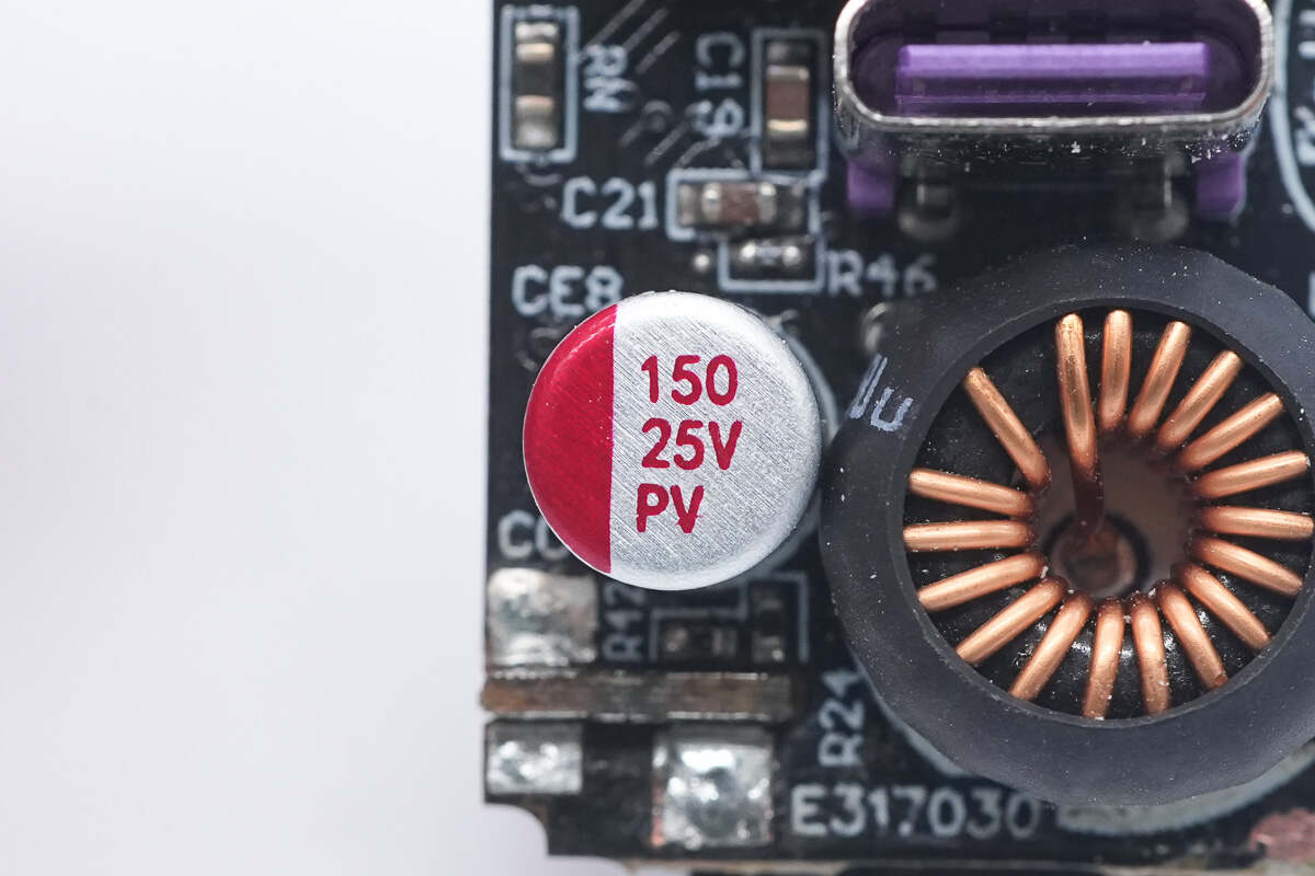
The other capacitor has the same specifications.
The buck inductor is insulated with heat shrink tubing.
The other buck inductor is also insulated with heat shrink tubing.
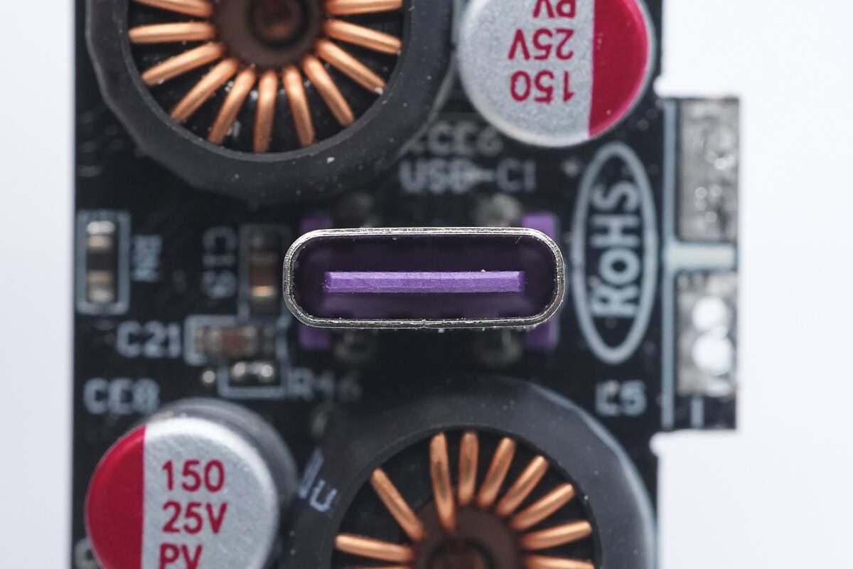
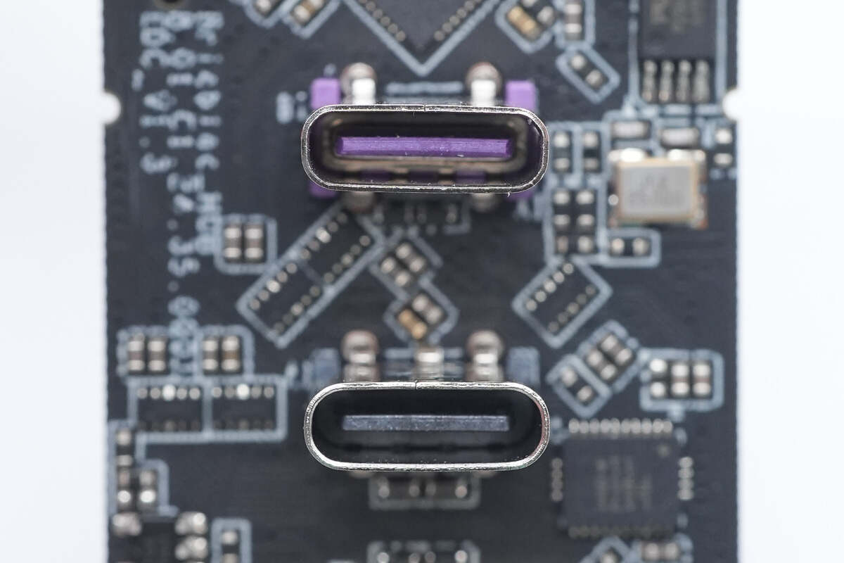
The USB-C socket has a purple plastic sheet.
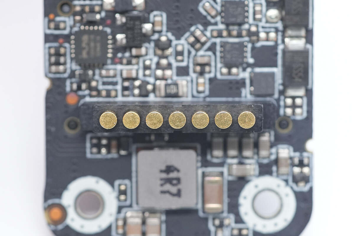
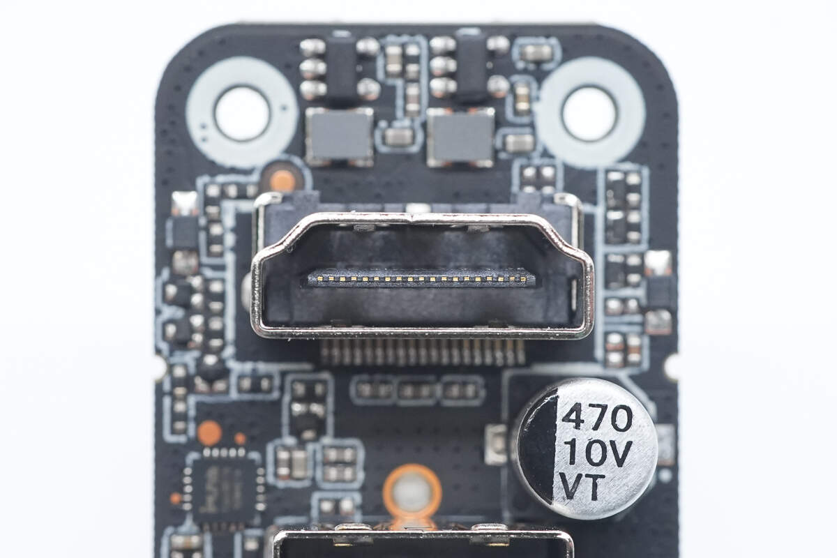
Close-up of the fast charging module’s Pogo Pin output contacts.
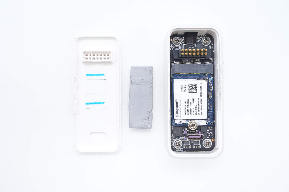
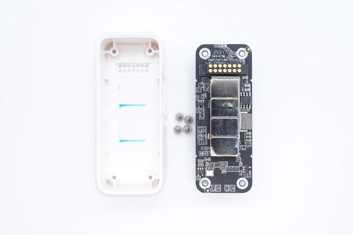
Open the SSD module casing along the seam.
Magnets are used to attach the docking station module.

On the other side, a thermal pad is attached to dissipate heat from the SSD.
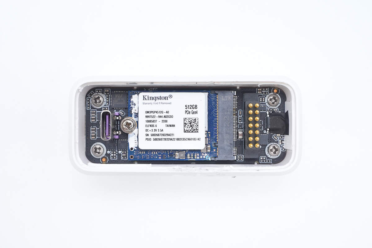
The PCBA module is secured inside the casing with screws.
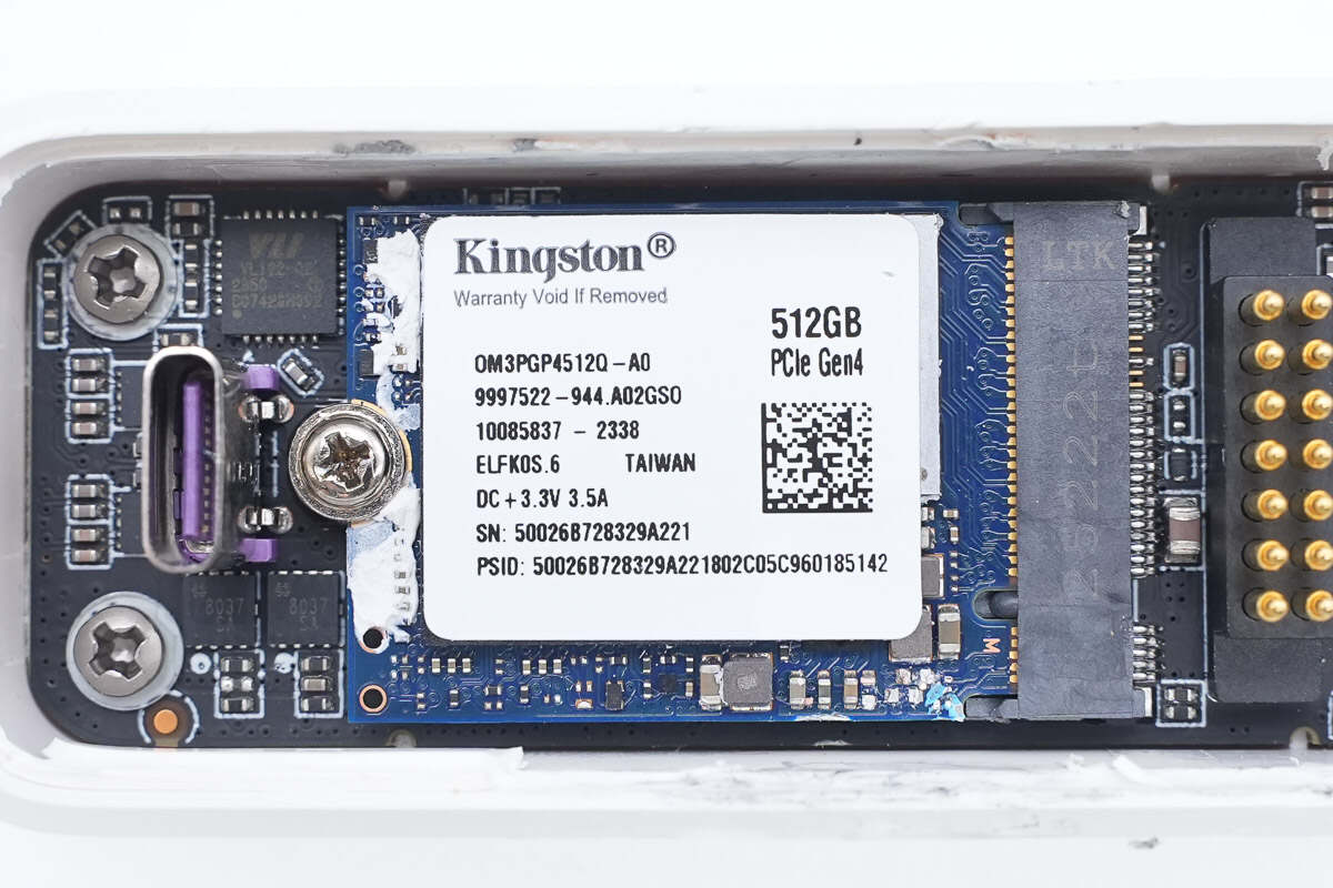
The solid-state drive is secured with screws, from Kingston, model OM3PGP4512Q-A0, with a capacity of 512GB. It features a PCIe Gen4 interface and uses the 2230 form factor.
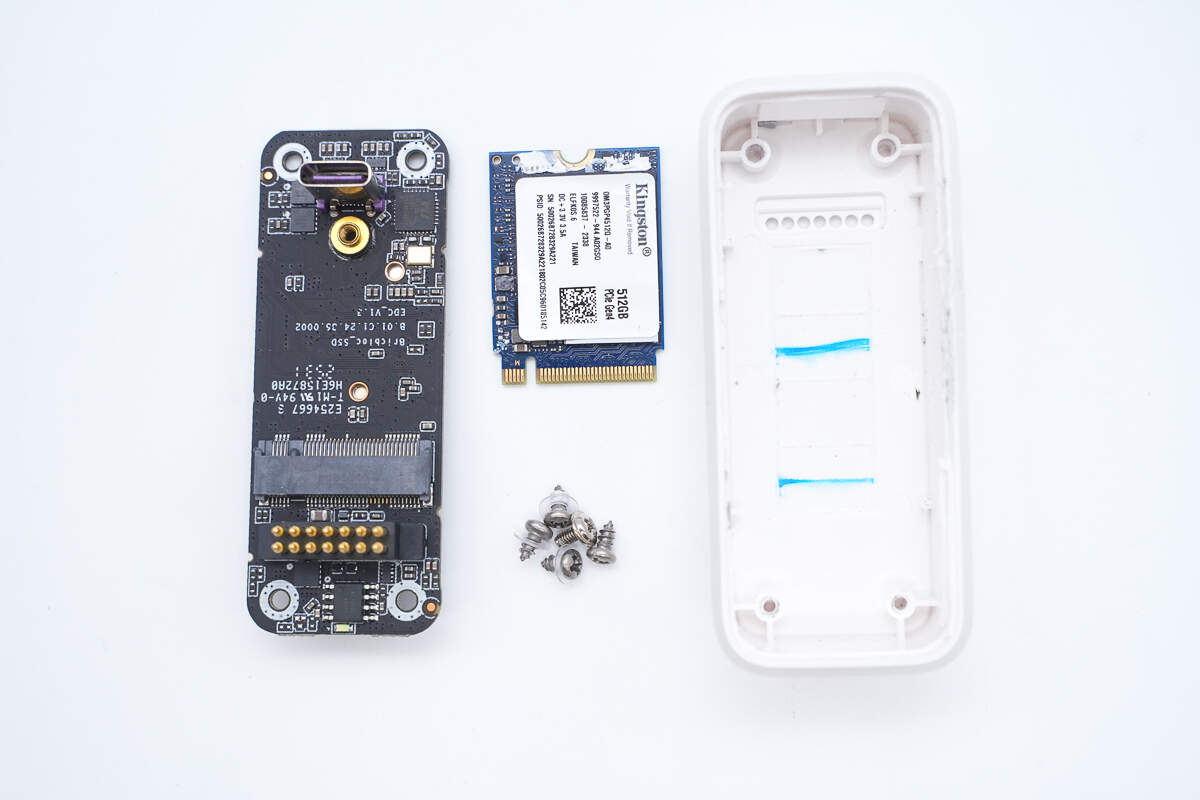
Remove the PCBA module.
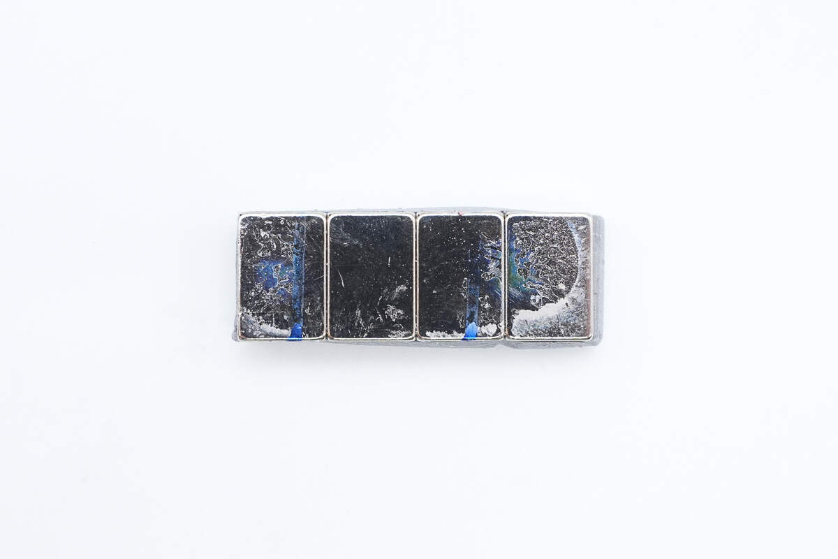
There are attachment magnets on the back side.
A thermal pad is placed between the magnets and the PCBA module.
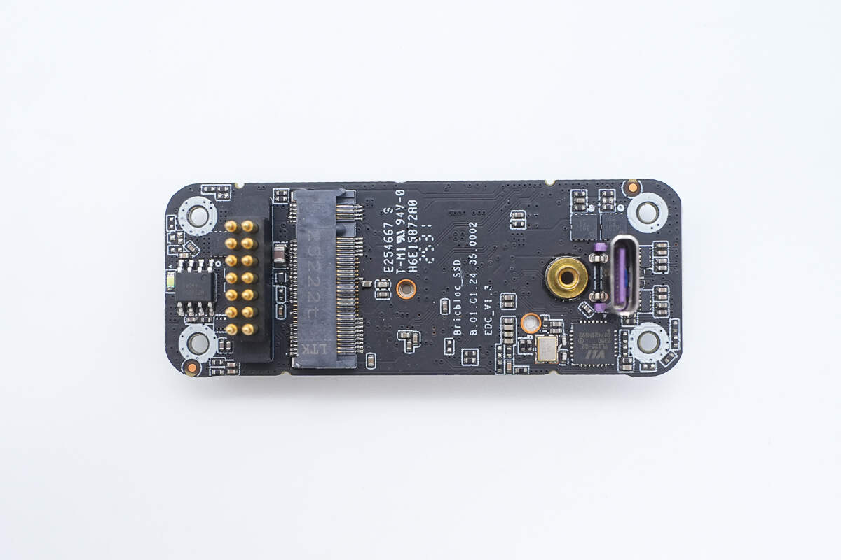
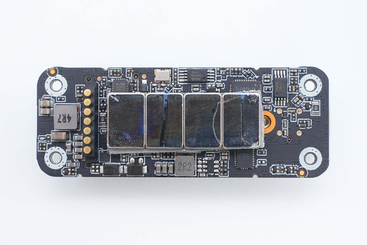
The front side of the PCB is equipped with a synchronous buck chip, Pogo Pin contacts, an M.2 SSD socket, a hub chip, VBUS switch MOSFETs, and a USB-C socket.
On the other side, there are buck inductors, a bridge chip, synchronous buck chips, a USB PD controller, memory chips, and a multiplexer.
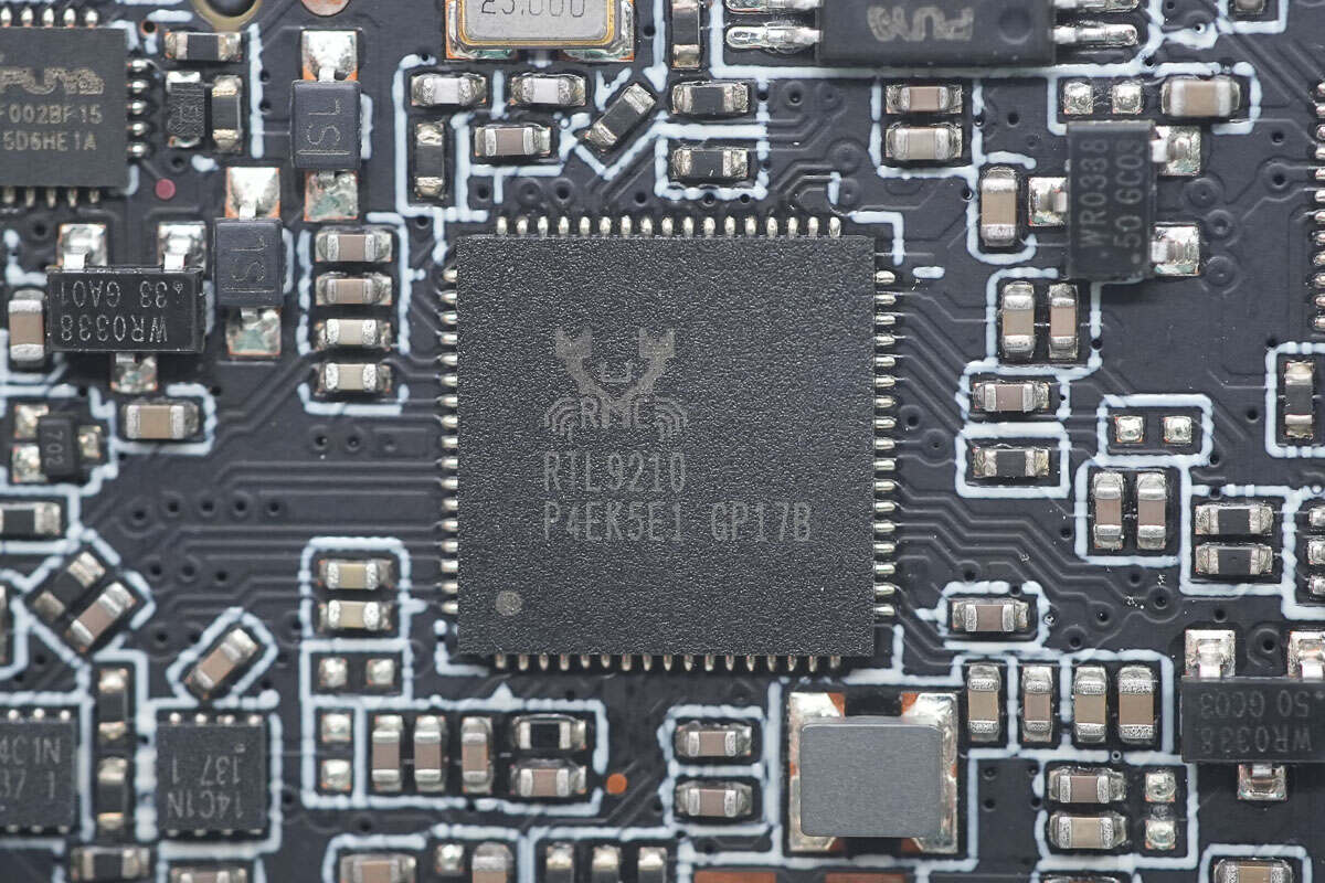
The SSD bridge chip is from REALTEK, model RTL9210. It converts USB 3.1 Gen2 to PCIe Gen 3x2, supports 10Gbps bandwidth, and comes in a QFN68 package.
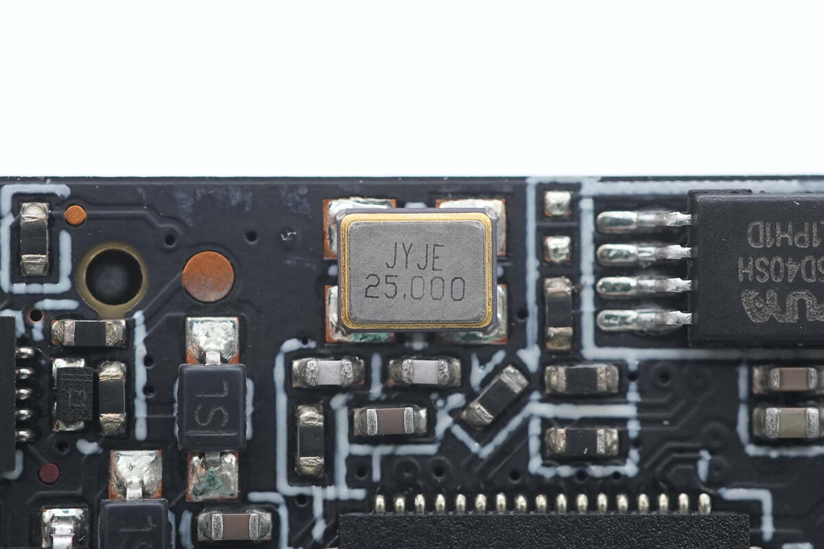
The clock crystal oscillator is from JYJE, with a frequency of 25.000 MHz.
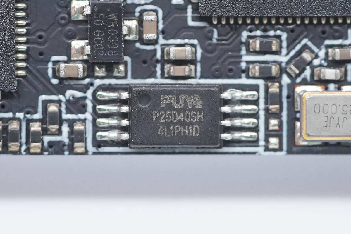
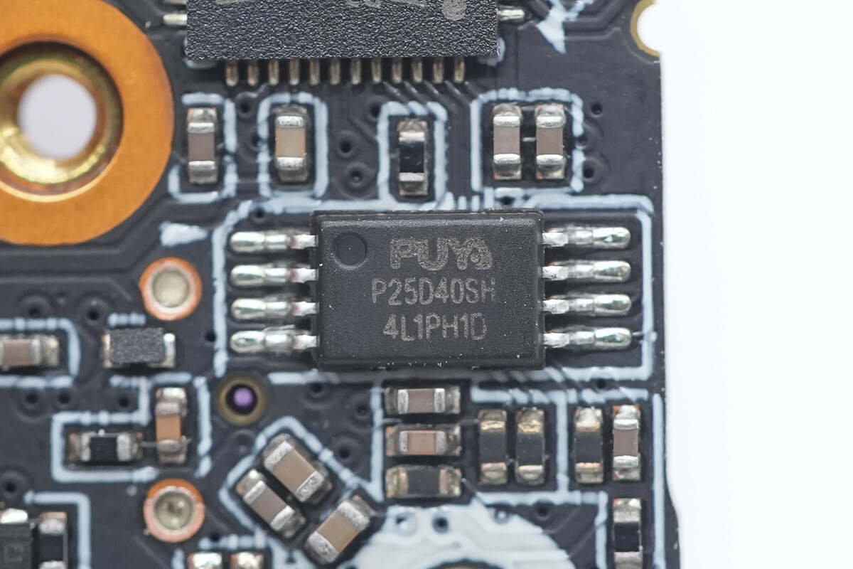
The memory chip is from Puya, model P25D40SH, with a capacity of 512KB. It supports a supply voltage of 2.3–3.6V and uses a TSSOP8 package.
Close-up of the buck inductor.
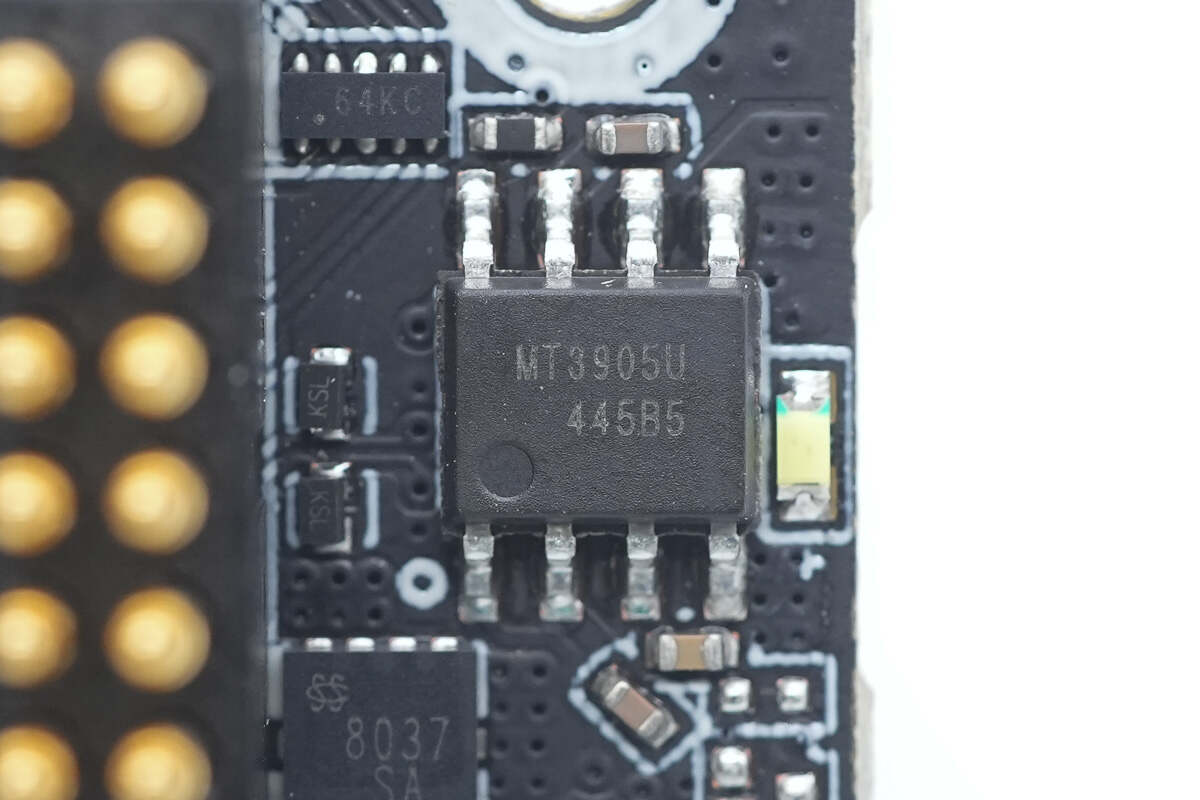
The synchronous buck chip is from M3TEK, model MT3905U. It is a synchronous buck converter with a 30V input voltage, 4A continuous output current, and 5A peak output current. It features built-in MOSFETs and comes in an SOP8-EP package.
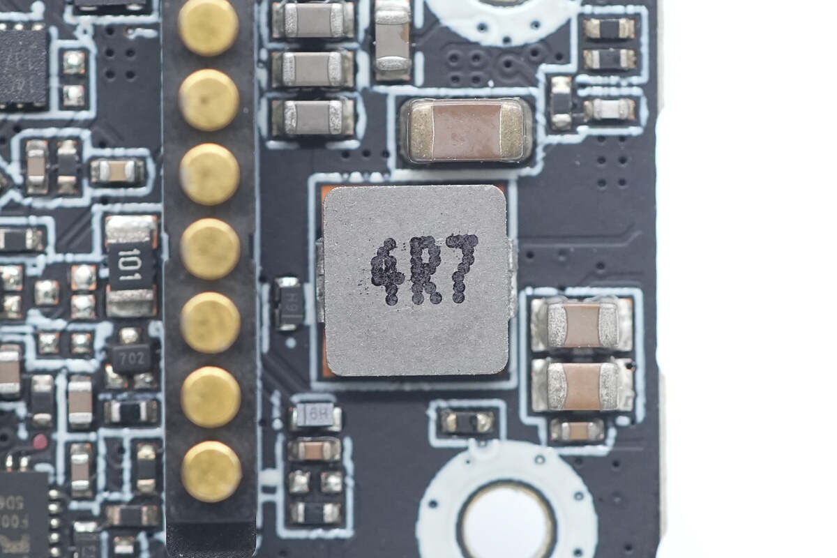
Close-up of the 4.7μH buck inductor.
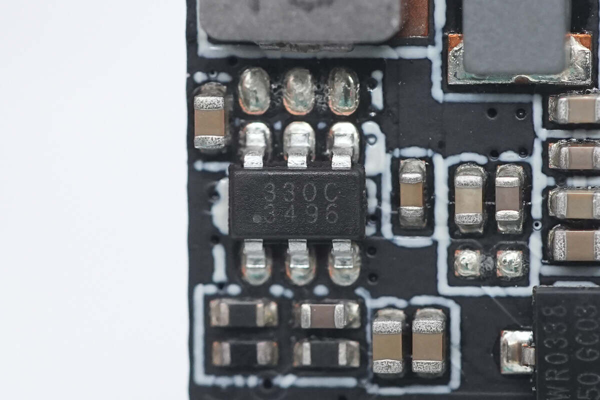
The synchronous buck chip is from SCT, marked with 330C, model SCT2330C. It is a synchronous buck converter with an input voltage range of 3.8–28V and an output current of 3A. It features integrated MOSFETs, supports output over-voltage protection and over-temperature protection, and comes in a TSOT23-6L package.
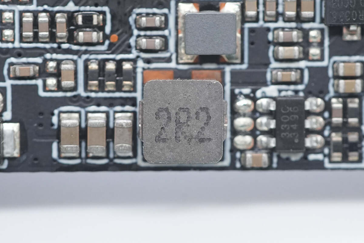
Close-up of the 2.2μH buck inductor.
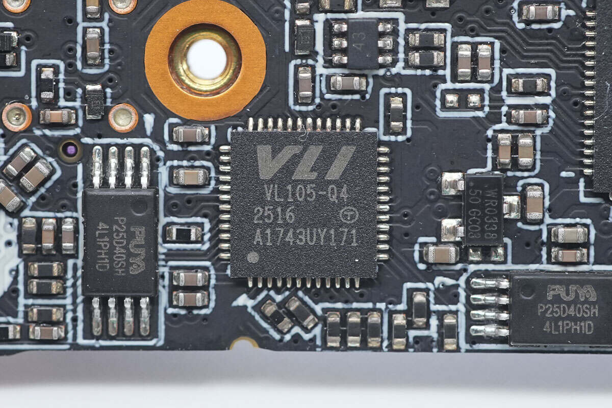
The USB-C interface controller is from VIA Labs, model VL105-Q4. It is used for USB-C interface and DisplayPort Alternate Mode control and comes in a QFN48 package.
The memory uses the Puya P25D40SH chip.
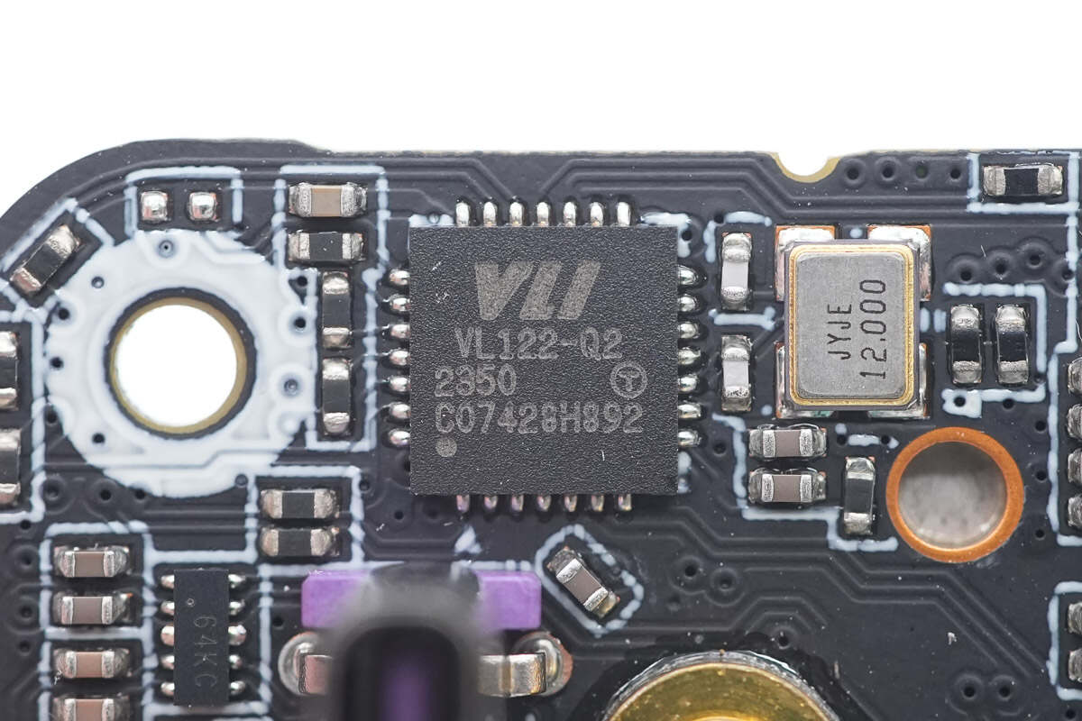
The hub chip is from VIA Labs, model VL122-Q2. It integrates 3.3V and 1.8V regulators, features four USB 2.0 ports, and supports configuration via EEPROM, SMBus, and I/O interfaces. It comes in a QFN28 package.
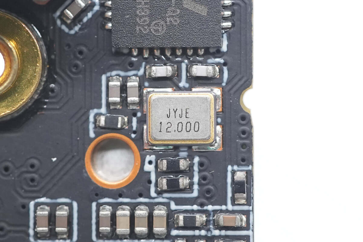
Close-up of the 12.000 MHz crystal oscillator.
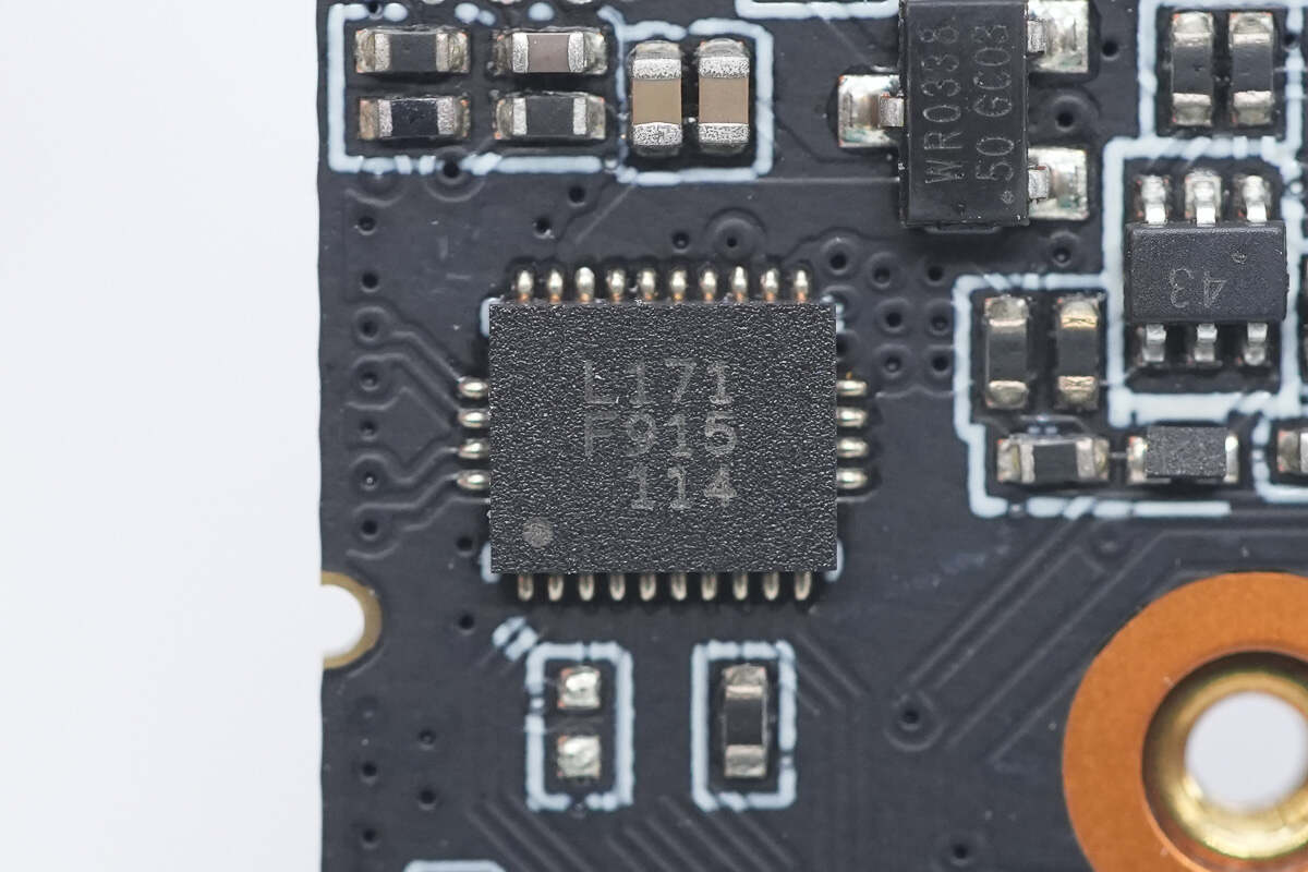
The VIA Labs VL171 is used for USB-C interface multiplexing and demultiplexing, outputting DisplayPort video signals and USB. It comes in a QFN-28 package.
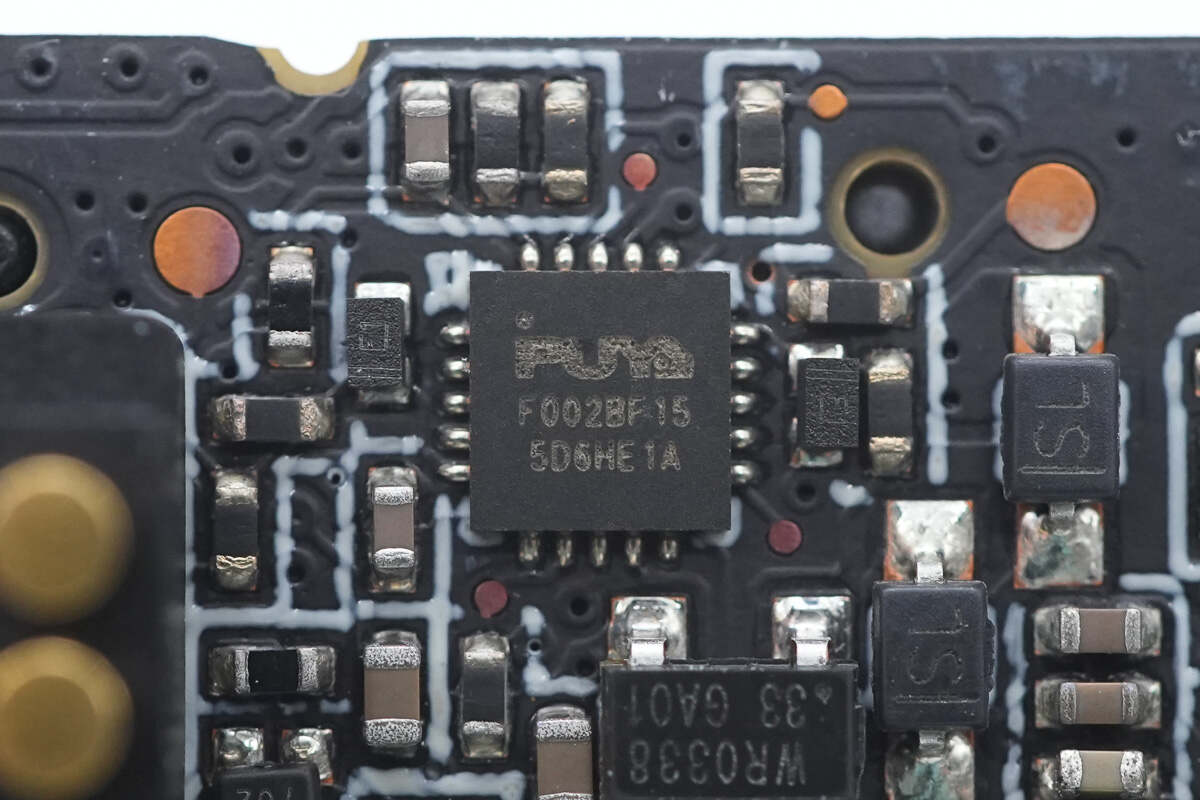
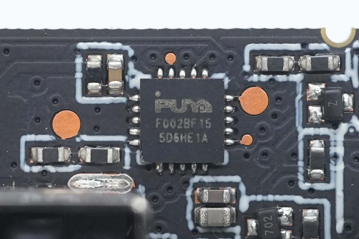
The MCU is from Puya, model PY32F002BF15. It features a built-in 32-bit ARM Cortex M0+ core with a clock speed of 24MHz, 24KB of FLASH memory, and 3KB of SRAM. It supports an operating voltage range of 1.7–5.5V and comes in a QFN20 package.
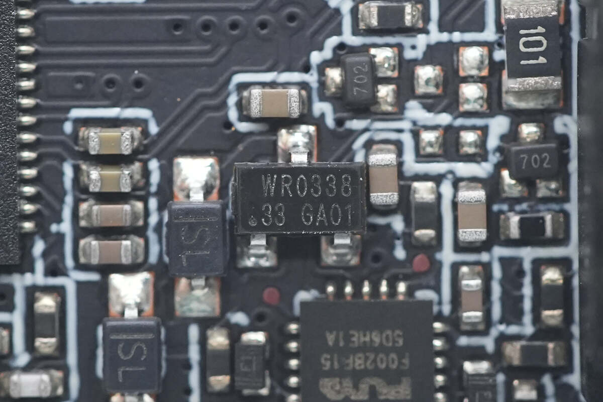
The voltage regulator chip is from WAYON, model WR0338. It is a linear regulator with an 18V input voltage, 300mA output current, and a 3.3V output voltage. It comes in an SOT23-3 package.
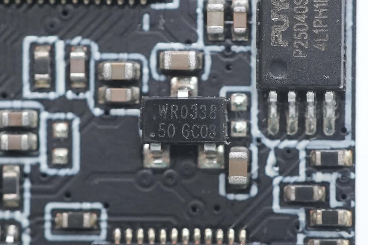
The other two voltage regulator chips have an output voltage of 5V.
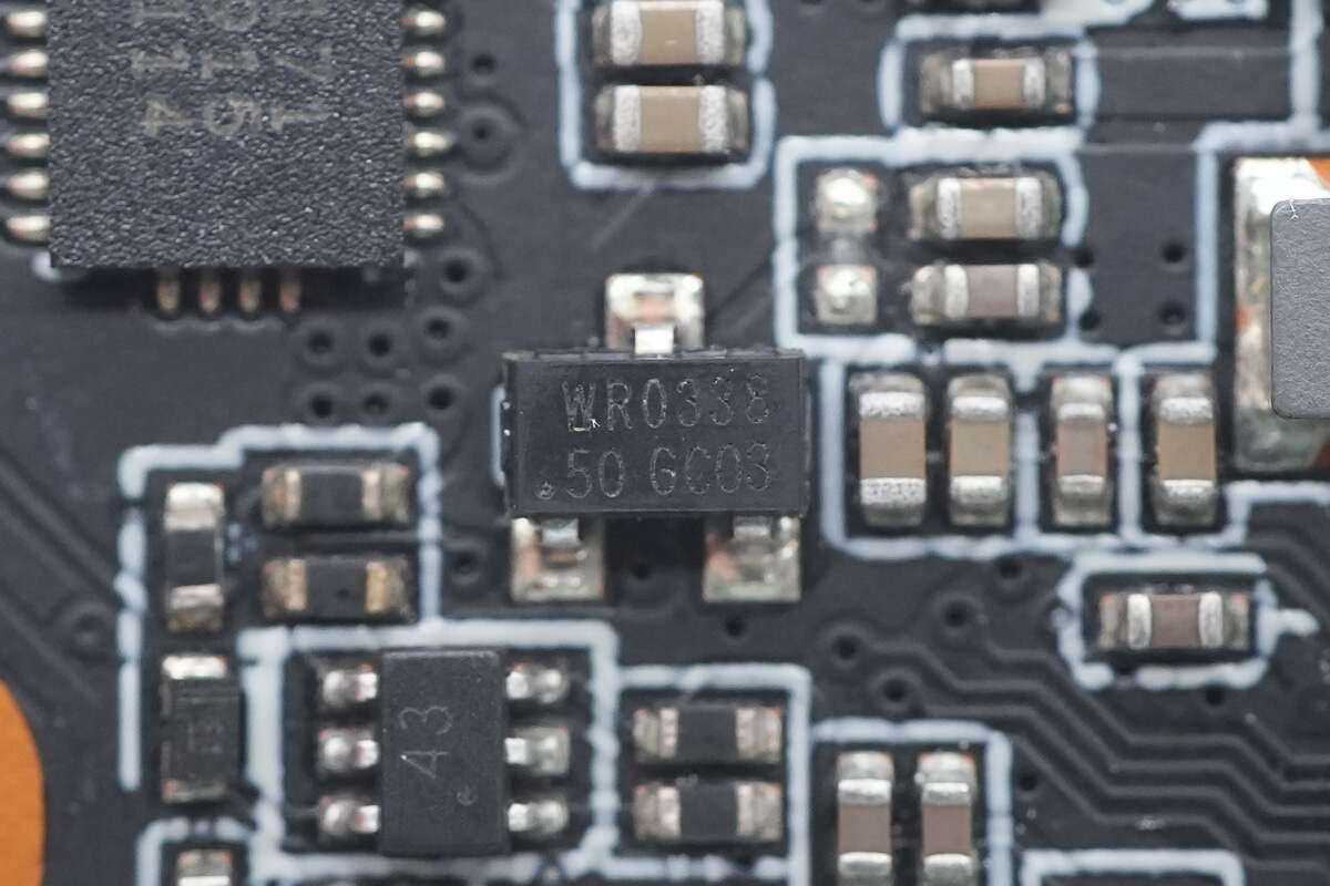
Close-up of the other 5V output voltage regulator chip.
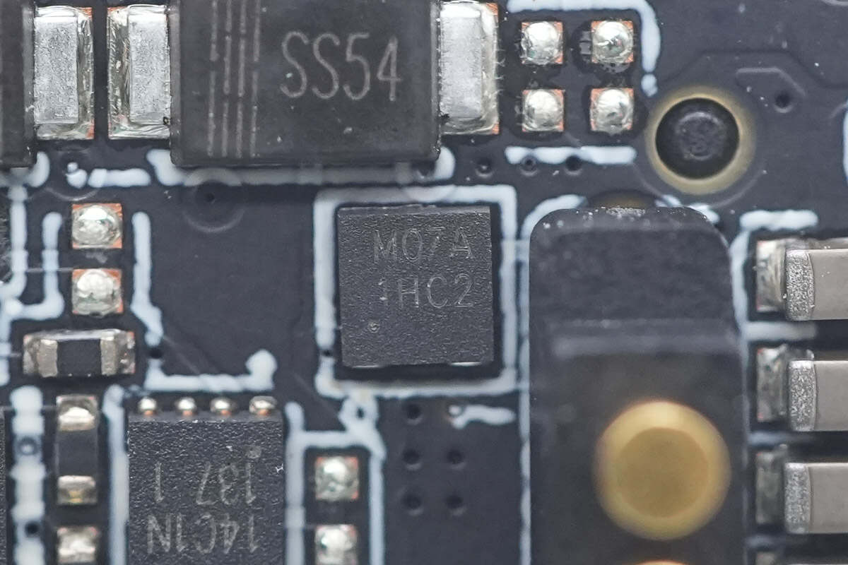
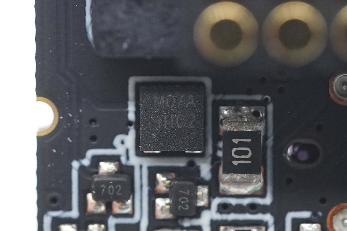
The TVS diode is marked with M07A, has a working voltage of 7V, and comes in a DFN2020 package.
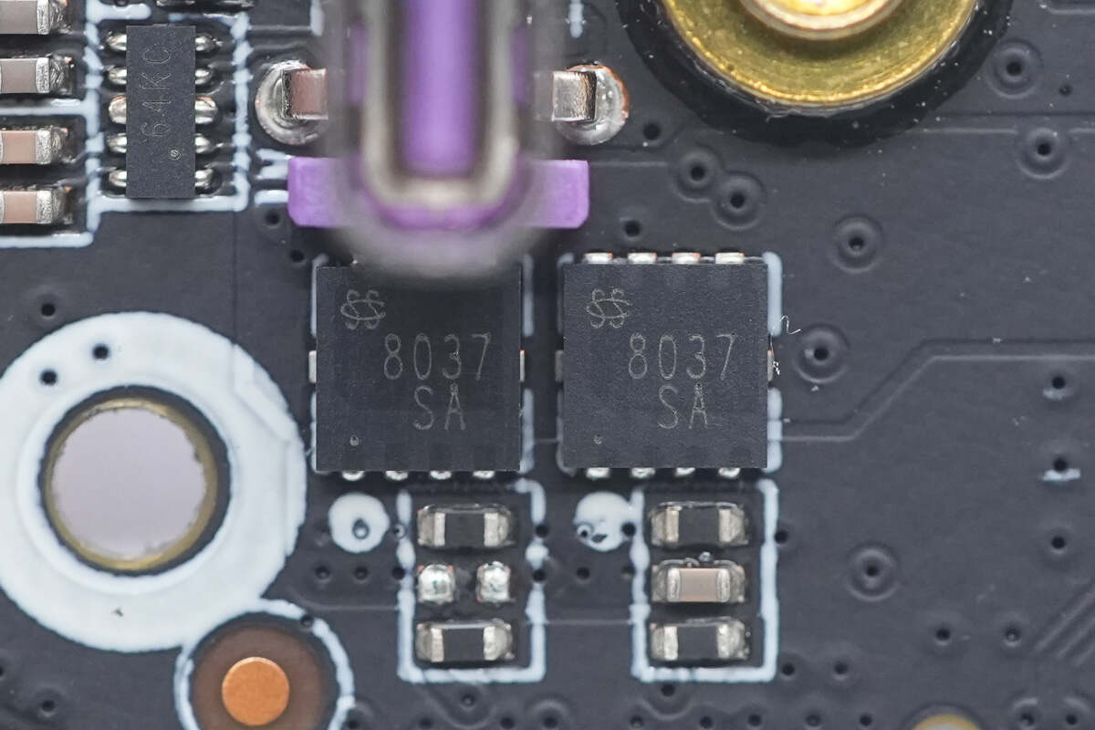
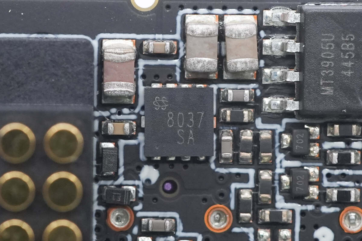
The VBUS MOSFETs are from SSC, model SSC8037GN2. They are PMOS devices with a voltage rating of -30V, an on-resistance of 14mΩ, and come in a DFN 2×2 package.
The other MOSFET has the same model.
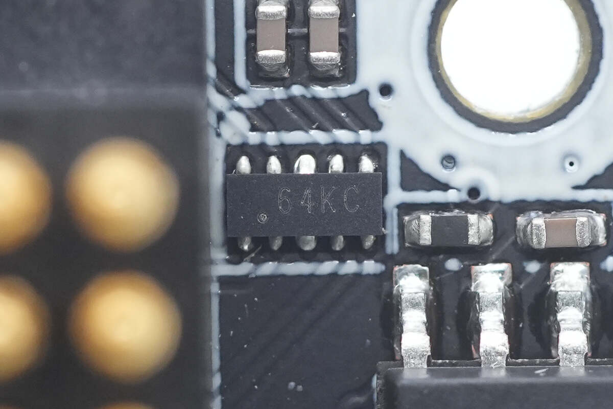
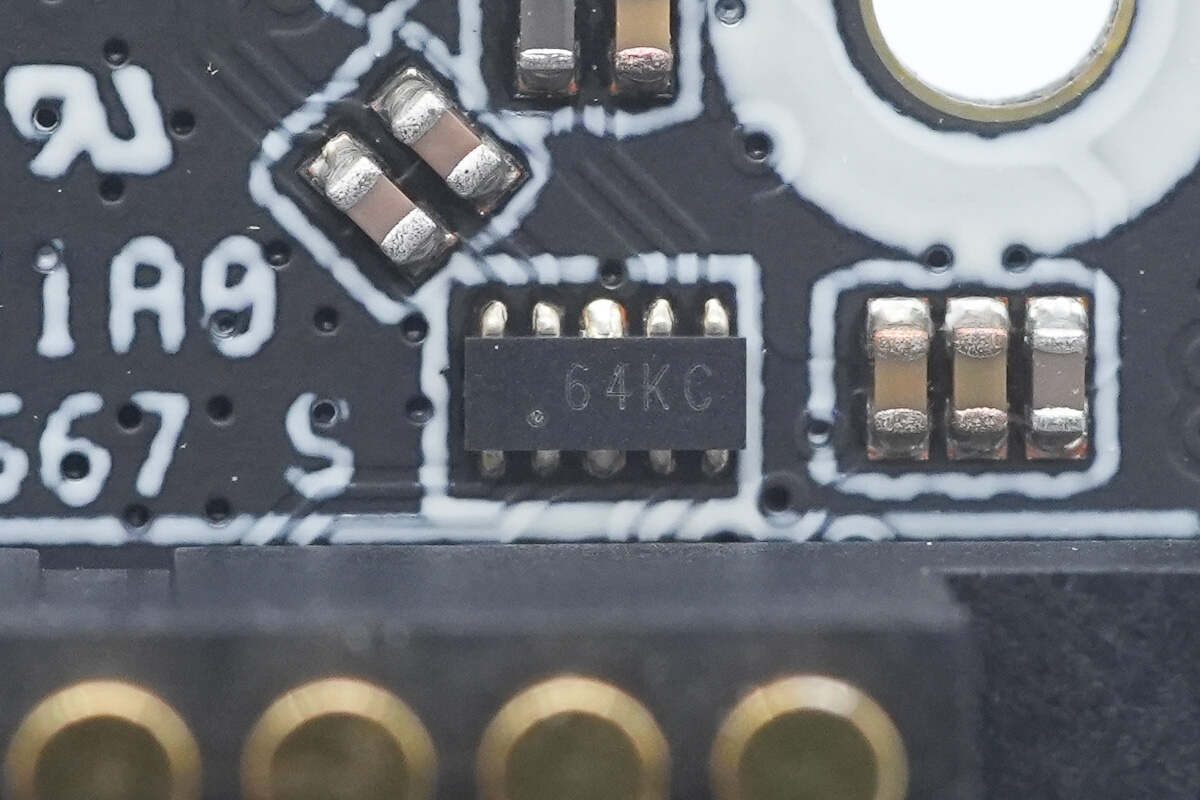
The TVS array is marked with 64KC.
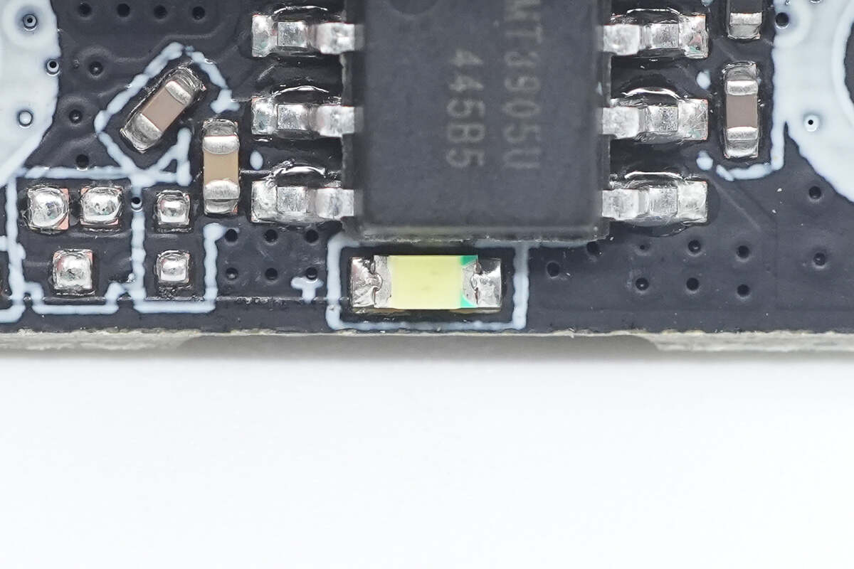
The SMD LED is used for operating status indication.
Close-up of the contacts connecting to the fast charging module.
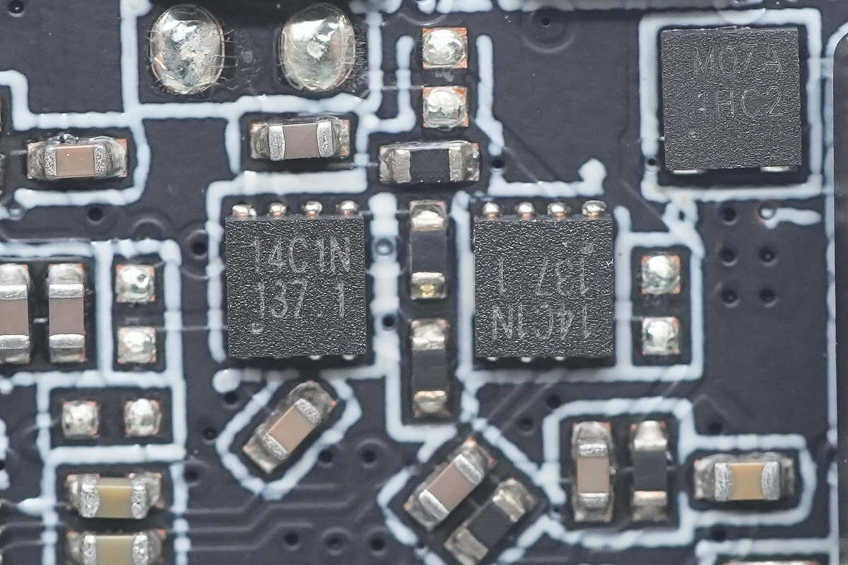
The overvoltage protection chips are from Prisemi, model P14C1N. They support a 32V input voltage tolerance, have an overvoltage protection threshold of 6V, support a 1.2A load current, and come in a DFN 2×2-8L package.
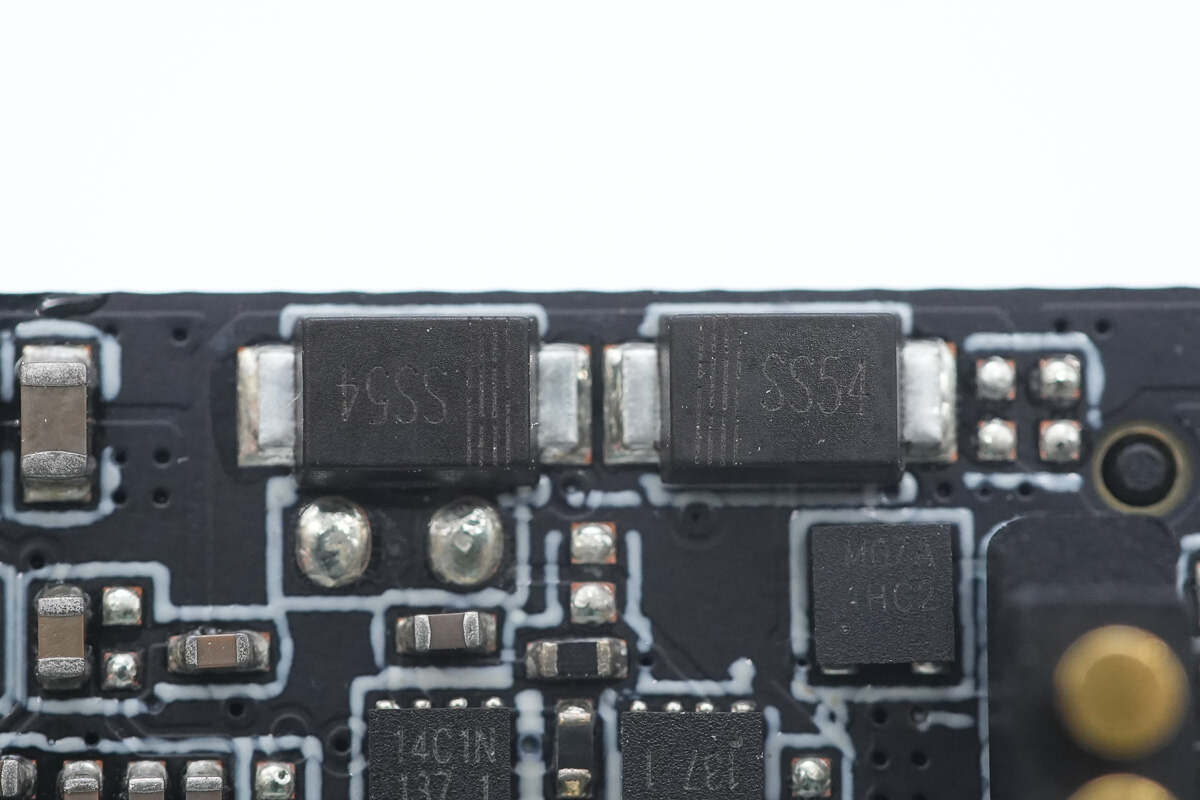
Close-up of the two SS54 Schottky diodes.
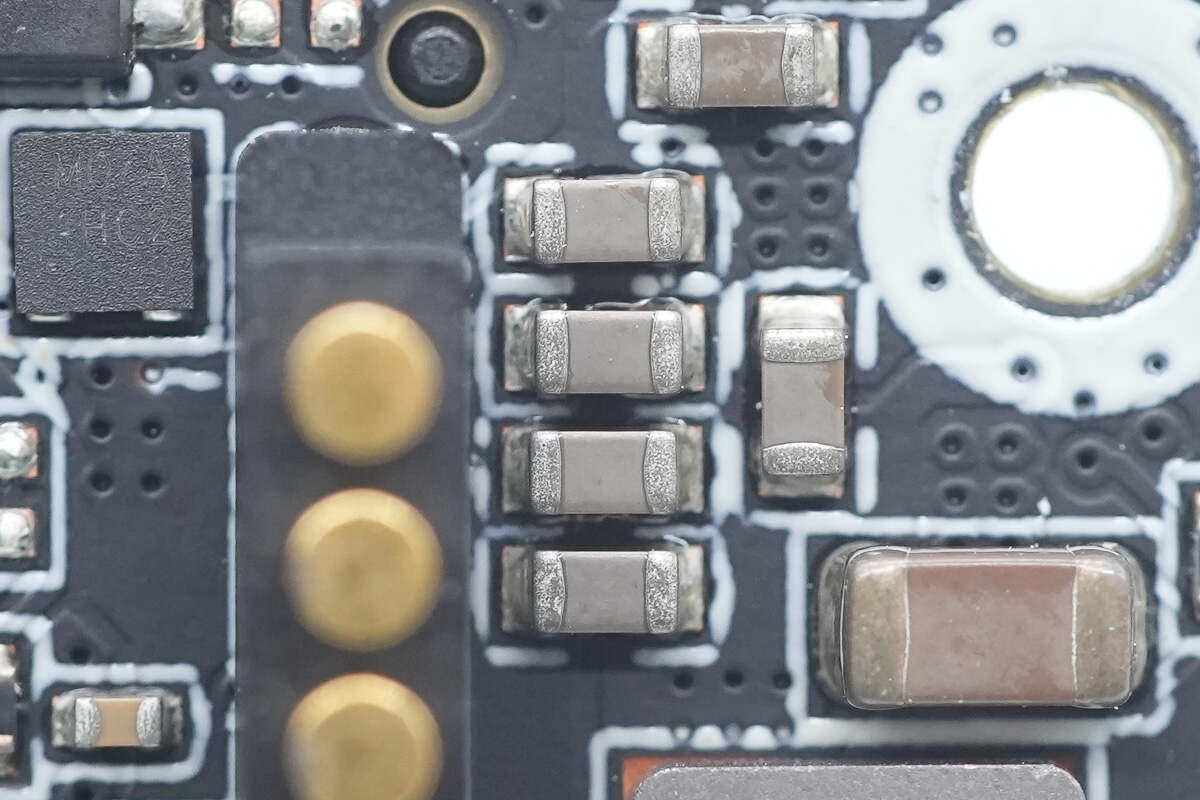
Close-up of the MLCC capacitors.
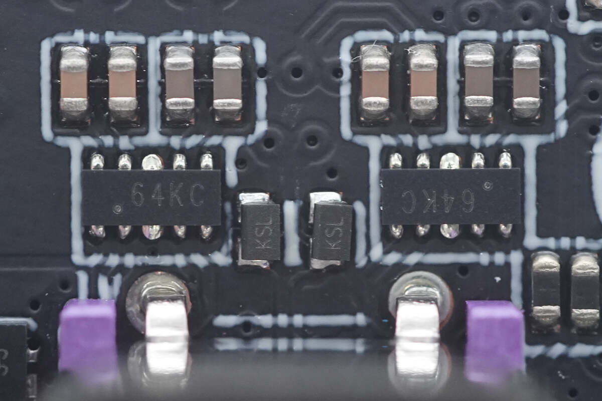
Close-up of the two TVS arrays marked with 64KC.
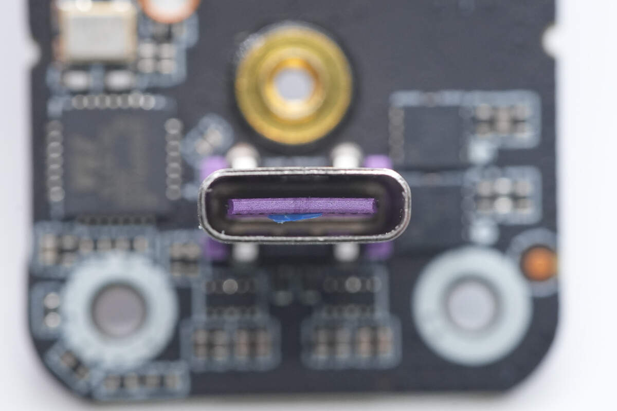
The USB-C socket has a purple plastic sheet.
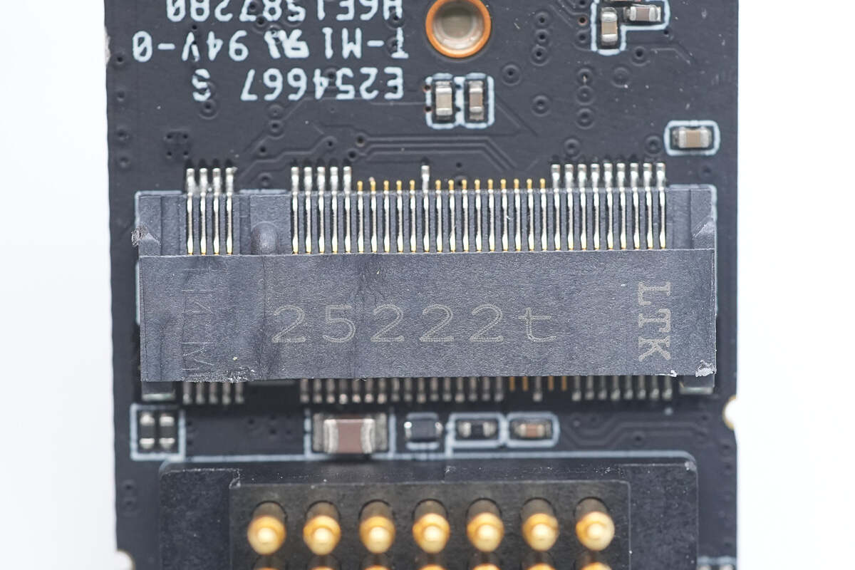
Close-up of the M.2 solid-state drive interface.
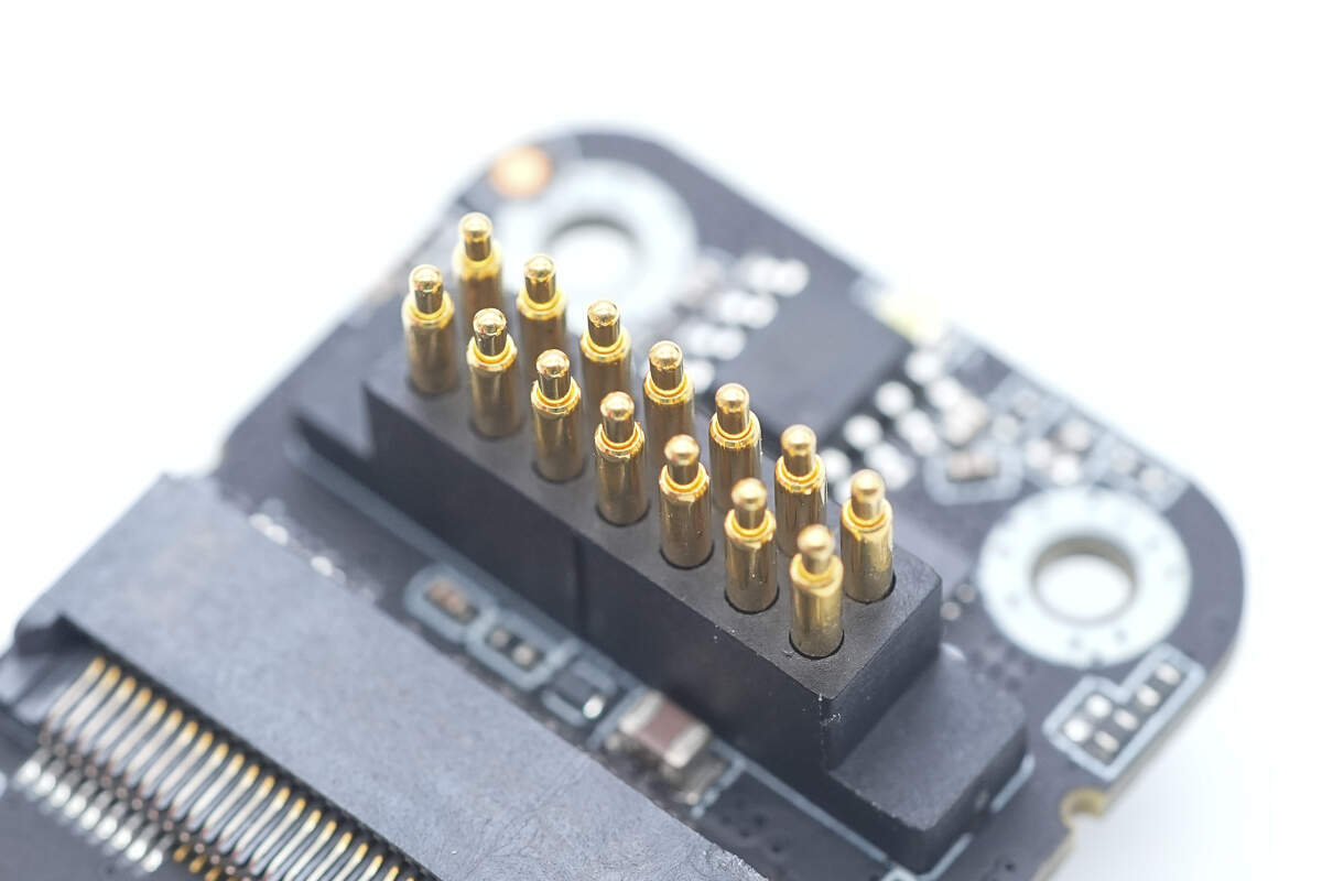
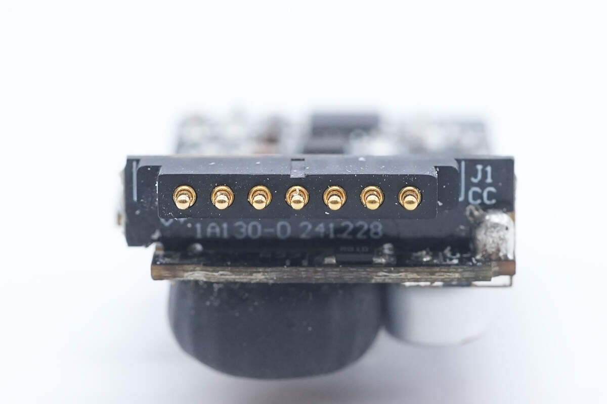
Close-up of the Pogo Pin contacts connecting to the docking station module.
Pry open the docking station module’s casing along the seam.
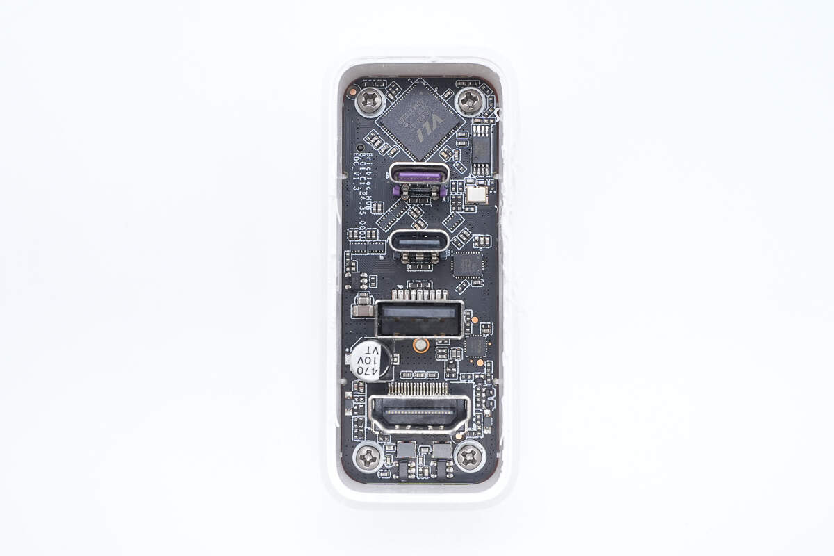
The PCBA module is secured inside the casing with screws.
Unscrew the screws. The magnets are attached to the back of the PCBA module.
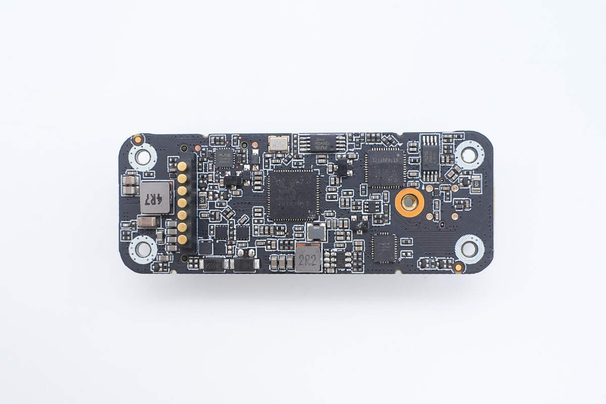
The front side of the PCBA features a hub chip, memory, multiplexer, MCU, and buck converter circuit.
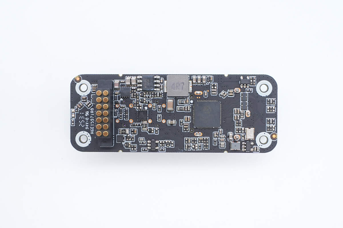
The back side is equipped with synchronous buck chips and a video conversion chip.
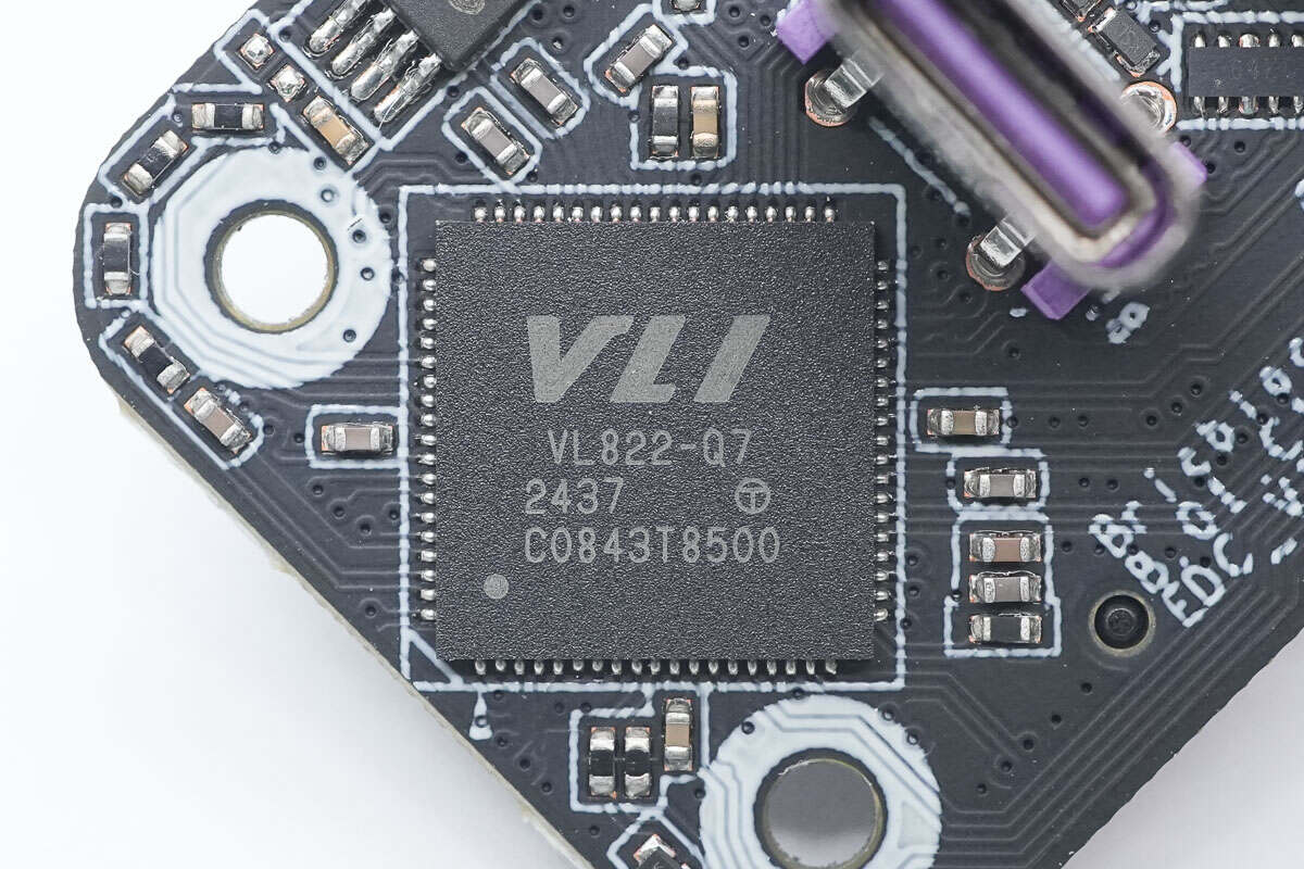
The USB hub chip is from VIA Labs, model VL822-Q7. It internally integrates an upstream port and two downstream port multiplexers, suitable for expanding four USB-A interfaces. It supports data rates up to 10Gbps and comes in a QFN-76 package.
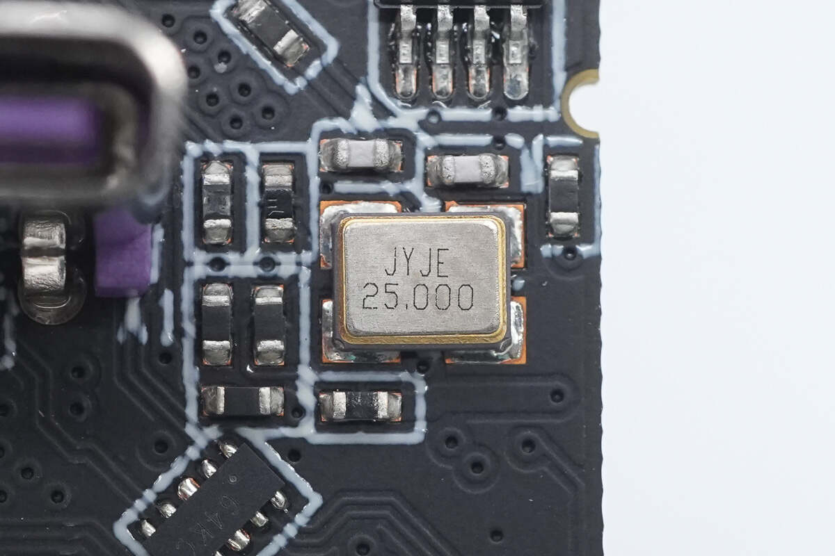
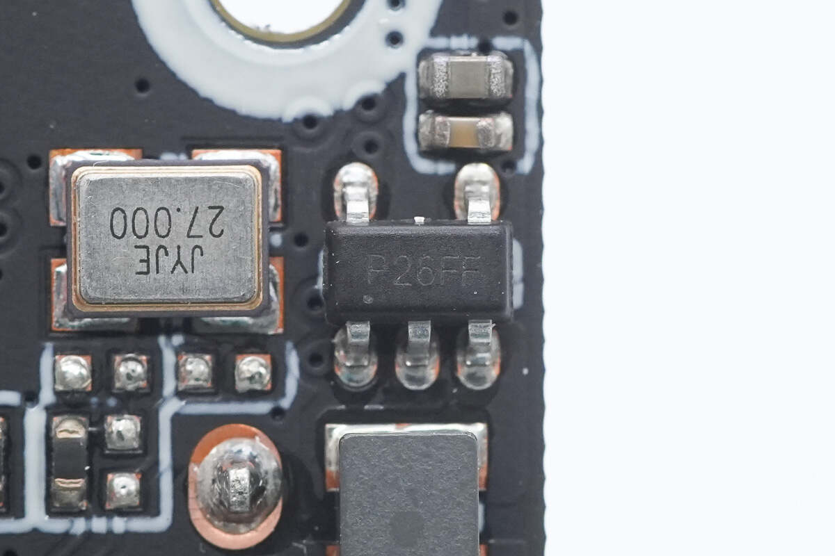
Close-up of the 25.000MHz clock crystal oscillator.
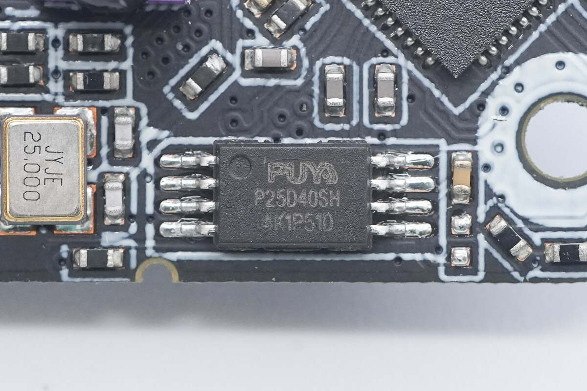
The memory uses the Puya P25D40SH.
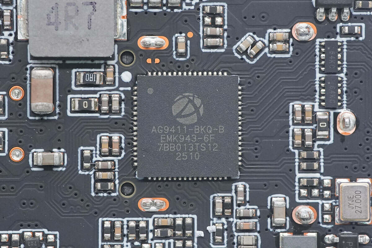
The video conversion chip is from ALGOLTEK, model AG9411. It is a DP1.4 to HDMI 2.0 converter, supporting 4K 60Hz video output, and comes in a QFN-64L package.
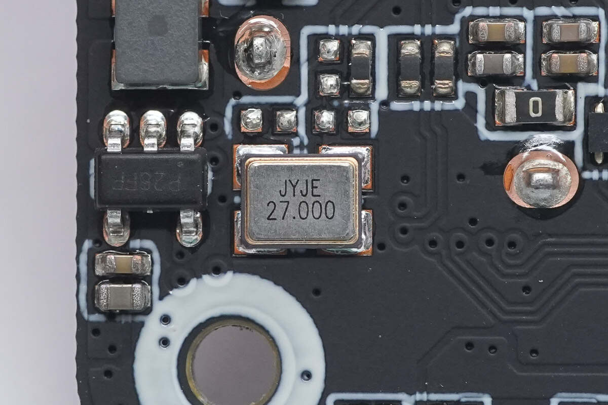
Close-up of the 27.000MHz clock crystal oscillator.
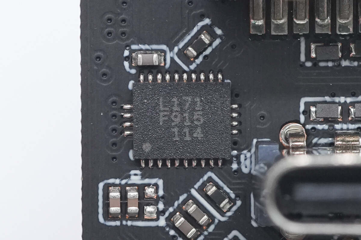
The VIA Labs VL171 is used for USB-C interface orientation switching.
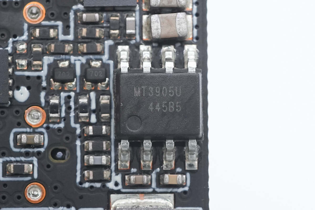
The synchronous buck chip uses the M3TEK MT3905U.
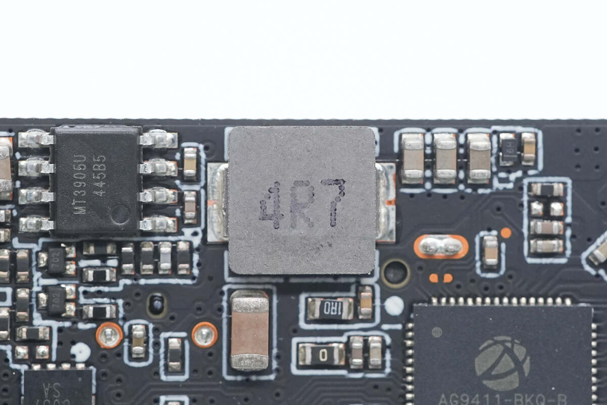
Close-up of the 4.7μH buck inductor.
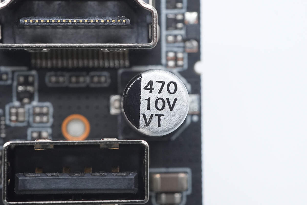
The filter capacitor has a specification of 470μF 10V.
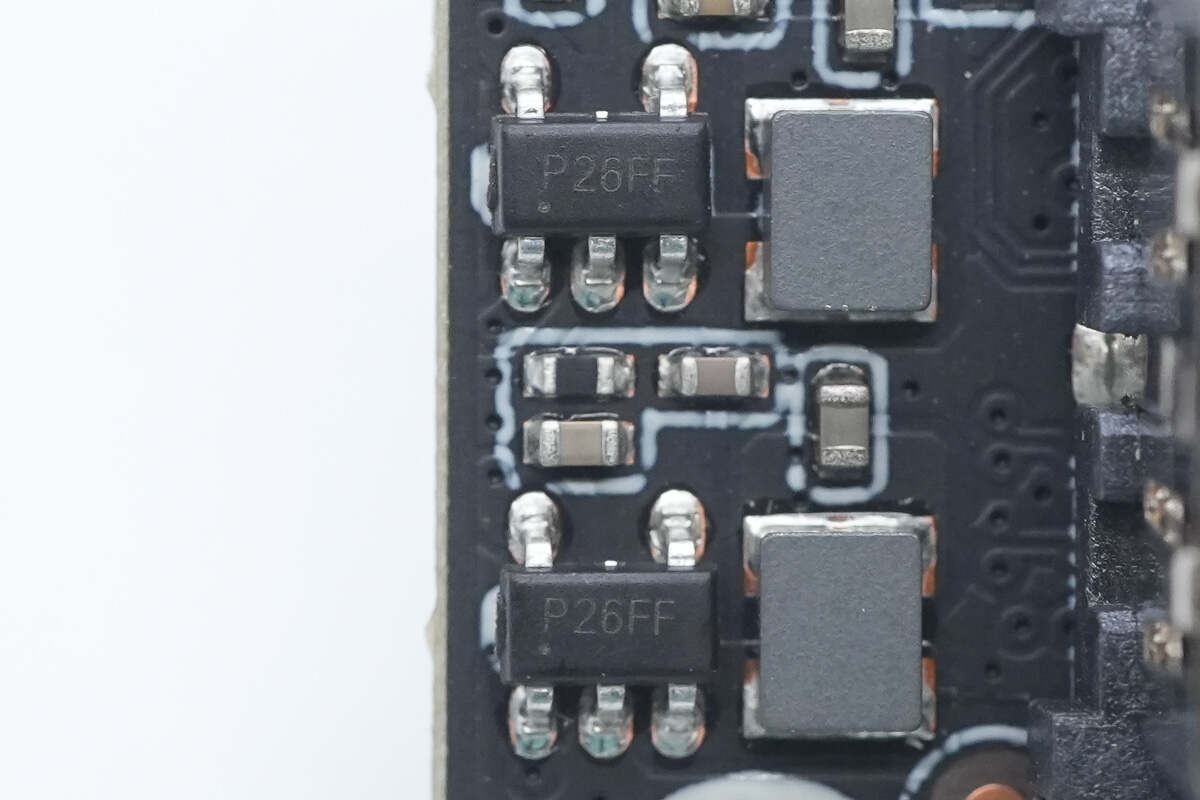
The synchronous buck chips are marked with P26FF.
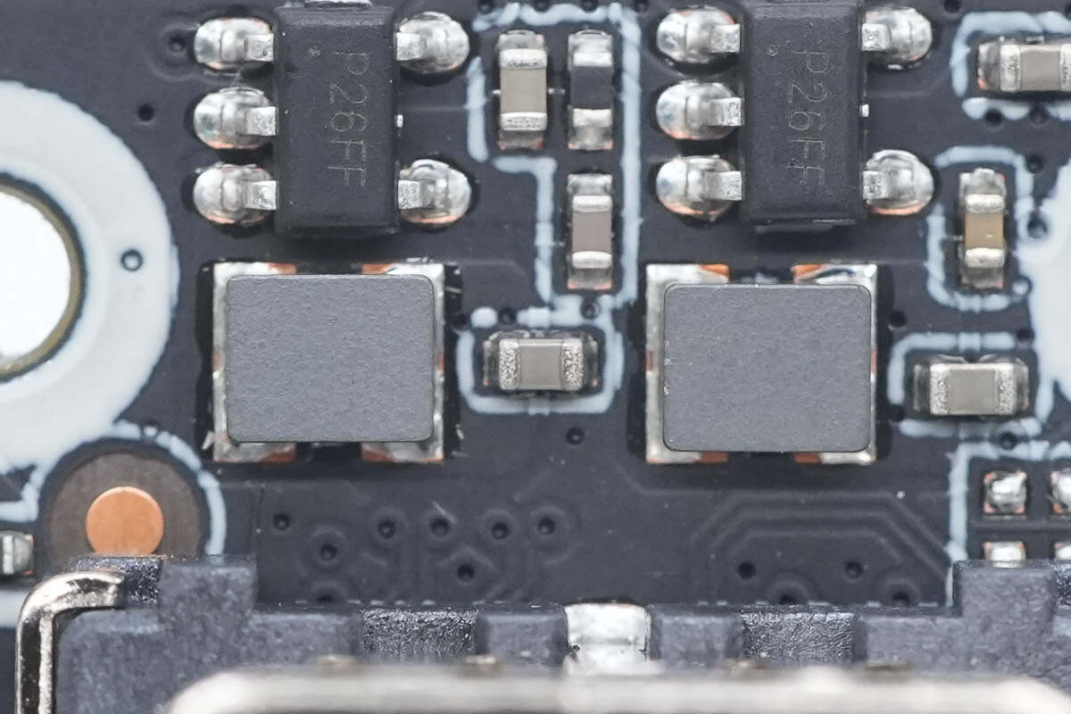
Close-up of the buck inductors.
The other synchronous buck chip is marked the same.
The MCU uses the Puya PY32F002BF15.
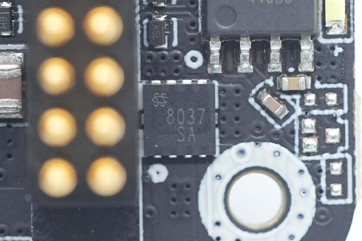
The VBUS MOSFET uses the SSC SSC8037GN2.
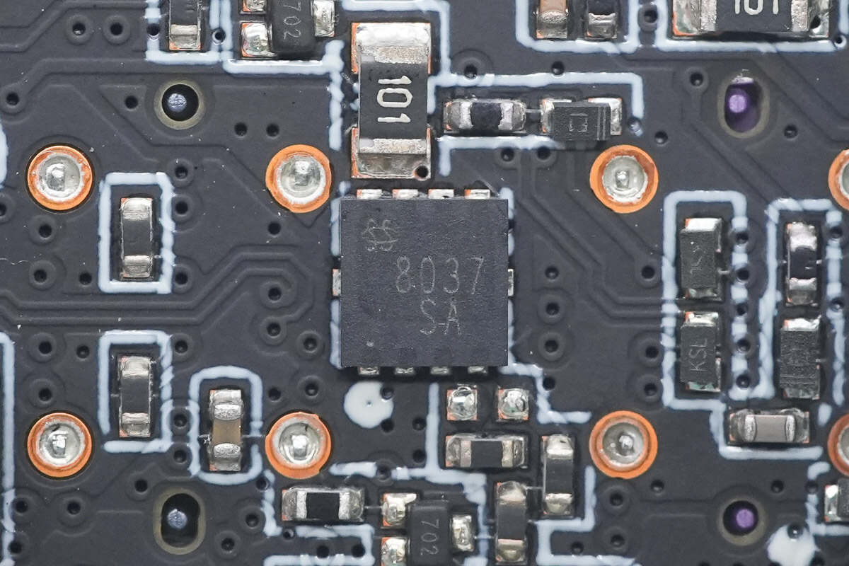
The other VBUS MOSFET has the same model.
The TVS diode is marked with M07A.
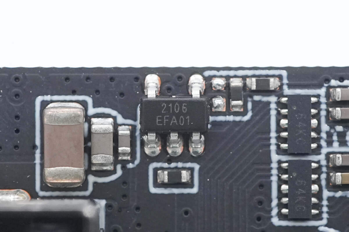
Close-up of the chip marked with EFA01.
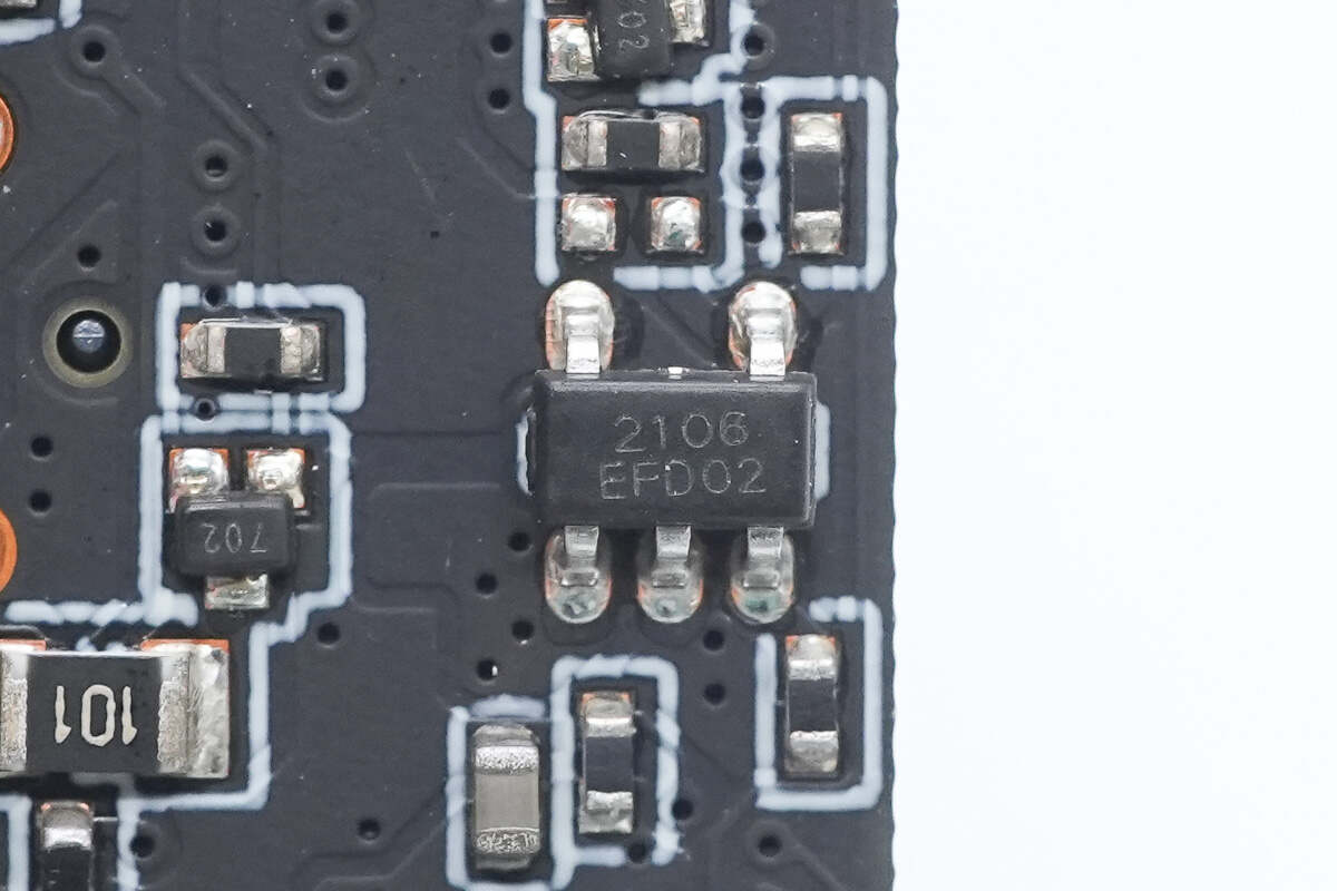
Close-up of the chip marked with EFD02.
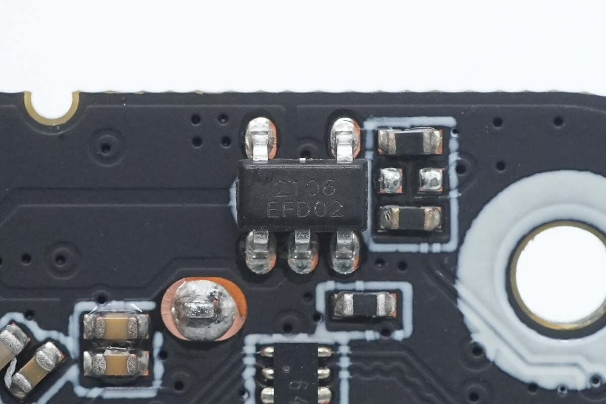
The other chip is marked the same.
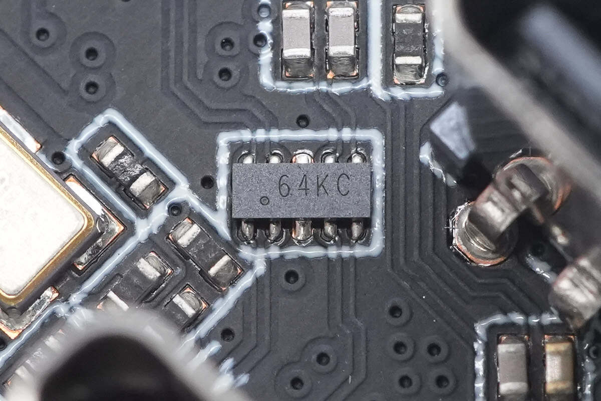
Close-up of the TVS array marked with 64KC.
The other TVS array has the same model.
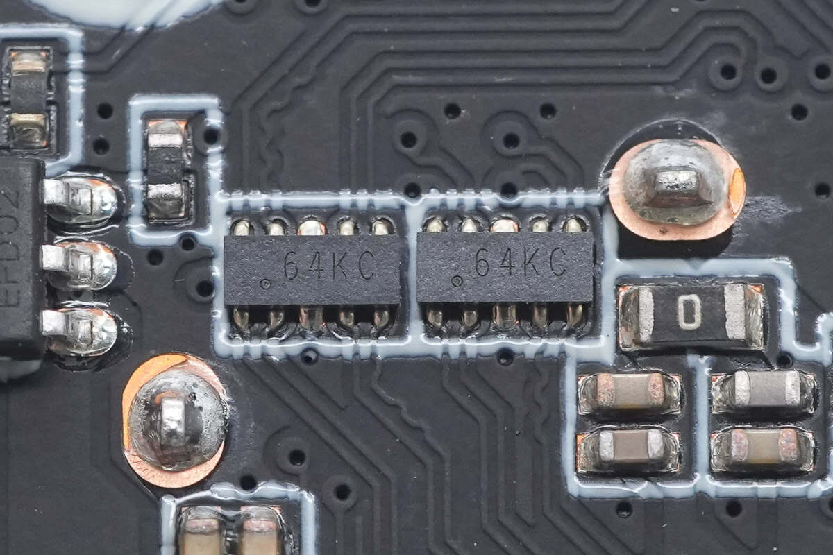
Close-up of the two TVS arrays marked with 64KC.
The USB-C sockets use through-hole soldering.
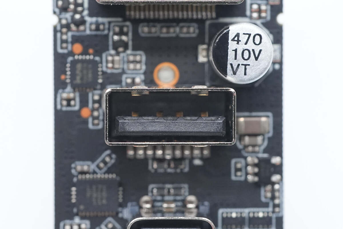
The USB-A port uses a black plastic sheet.
The HDMI interface uses through-hole soldering.
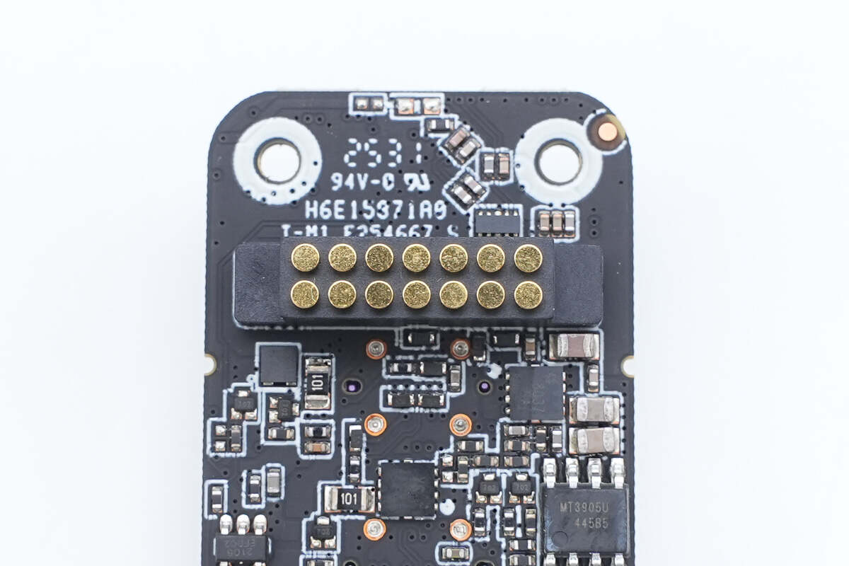
Close-up of the Pogo Pin contacts connecting to the SSD module.

Well, those are all components of the BricBloc 67W All-in-One Charger.
Summary of ChargerLAB
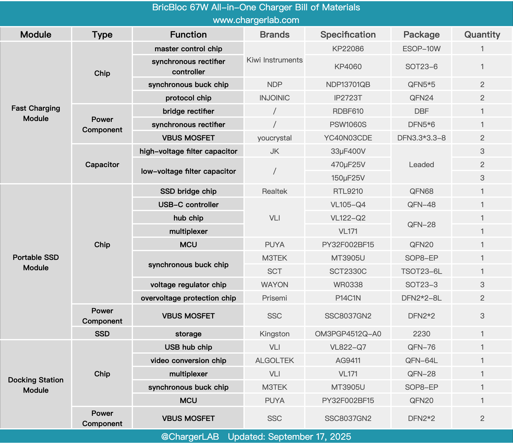
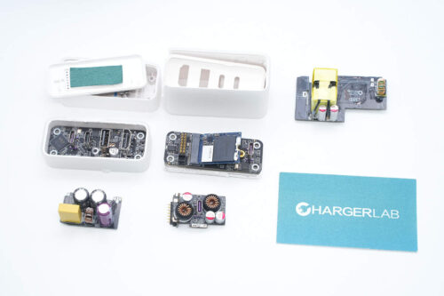
Here is the component list of the BricBloc 67W All-in-One Charger for your convenience.
The complete solution consists of a 67W GaN fast charging module, a 512GB portable solid-state module, and a four-port docking module. The modules connect via Pogo Pin contacts and are secured with magnetic attraction. It integrates charging, storage, and expansion functions, features 10Gbps high-speed transmission capability, and supports 4K 60Hz HDMI output.
After taking it apart, we found that it uses a Kiwi Instruments power supply solution, featuring a built-in KP22086 GaN monolithic chip and KP4060 synchronous rectifier controller. It employs two Injoinic IP2723T protocol chips paired with two NDP NDP13701QB synchronous buck converters to achieve dual-port fast charging output.
The SSD module contains a Kingston 512GB solid-state drive. It uses a REALTEK RTL9210 for drive bridging, VIA Labs VL105-Q4 for USB-C interface control, VL122-Q2 for USB port expansion, and a Puya MCU for overall control.
The docking module is equipped with a VIA Labs VL822-Q7 hub chip for USB interface expansion and uses an ALGOLTEK AG9411 for DP to HDMI conversion. The modules are magnetically attached. The PCBA modules have thermal pads to ensure effective heat dissipation. The internal workmanship is solid, and the components used are reliable.
Related Articles:
1. Teardown of EcoFlow RAPID 170W 25,000mAh Power Bank with Built-in Cable (EF-HB-001)
2. Teardown of Apple iPhone Air MagSafe Battery (A3466)
3. Teardown of Apple 40W Dynamic Power Adapter with 60W Max (A3365)