Introduction
We have acquired Apple’s newly released Hong Kong version of the MagSafe charger, model A3502. The cable is 1 meter in length, with a 2-meter version also available. As with previous designs, the cable features a braided exterior for added durability.
The new MagSafe charger is Qi2.2 certified, supporting both Qi2 25W wireless charging and standard Qi wireless charging. When used with a 30W power adapter, it can deliver up to 25W of wireless power to supported new-generation devices, reaching 50% charge in just 30 minutes. Next, we’ll examine the internal components and the build quality of it.
Product Appearance
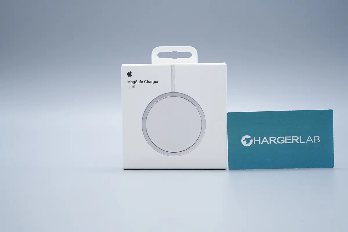
The white packaging box features the Apple logo, the words "MagSafe Charger," and an image of the product itself.
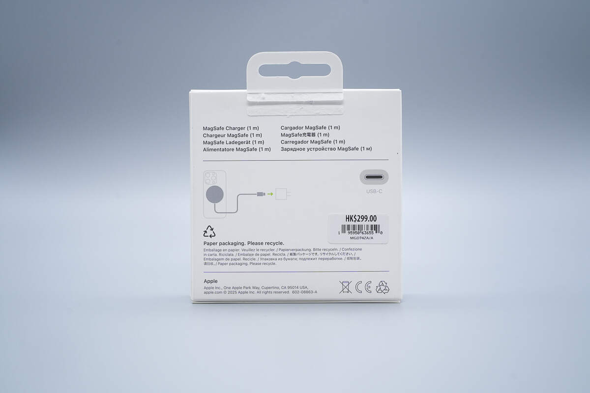
The back of the box displays the product name in multiple languages, a usage illustration, and certification marks, including CE approval.
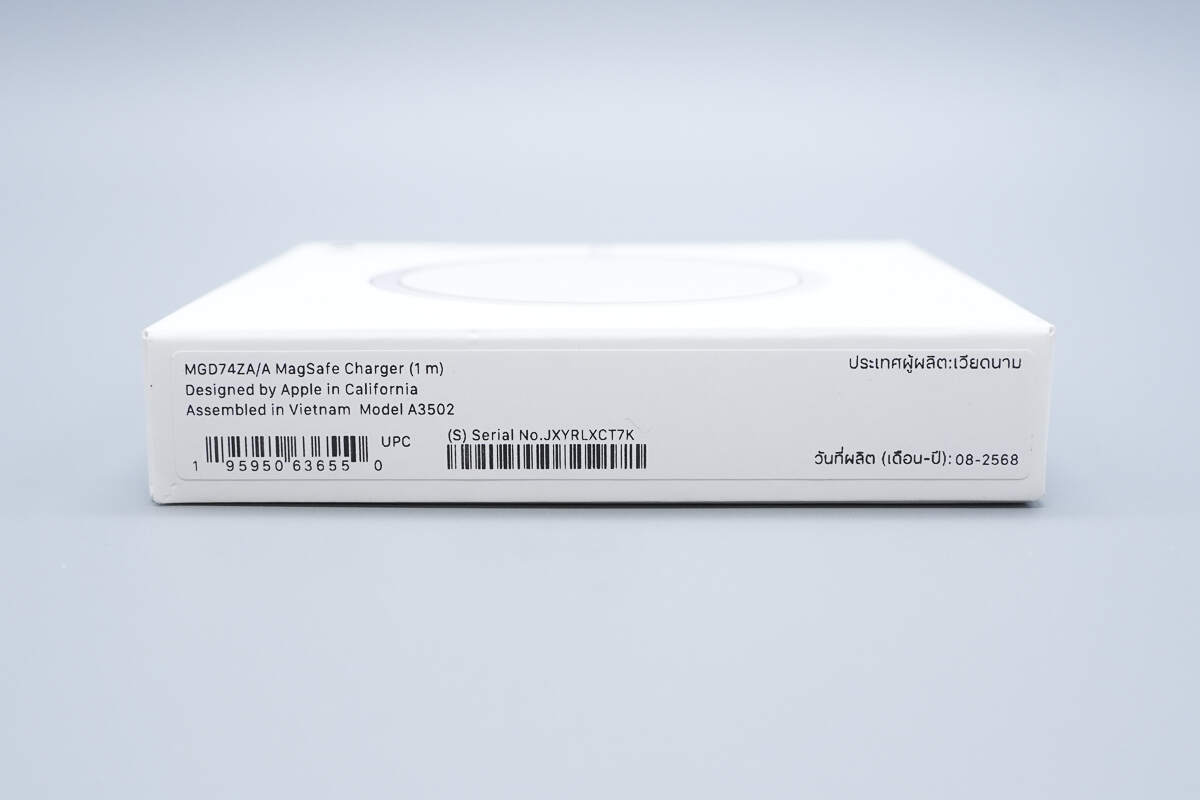
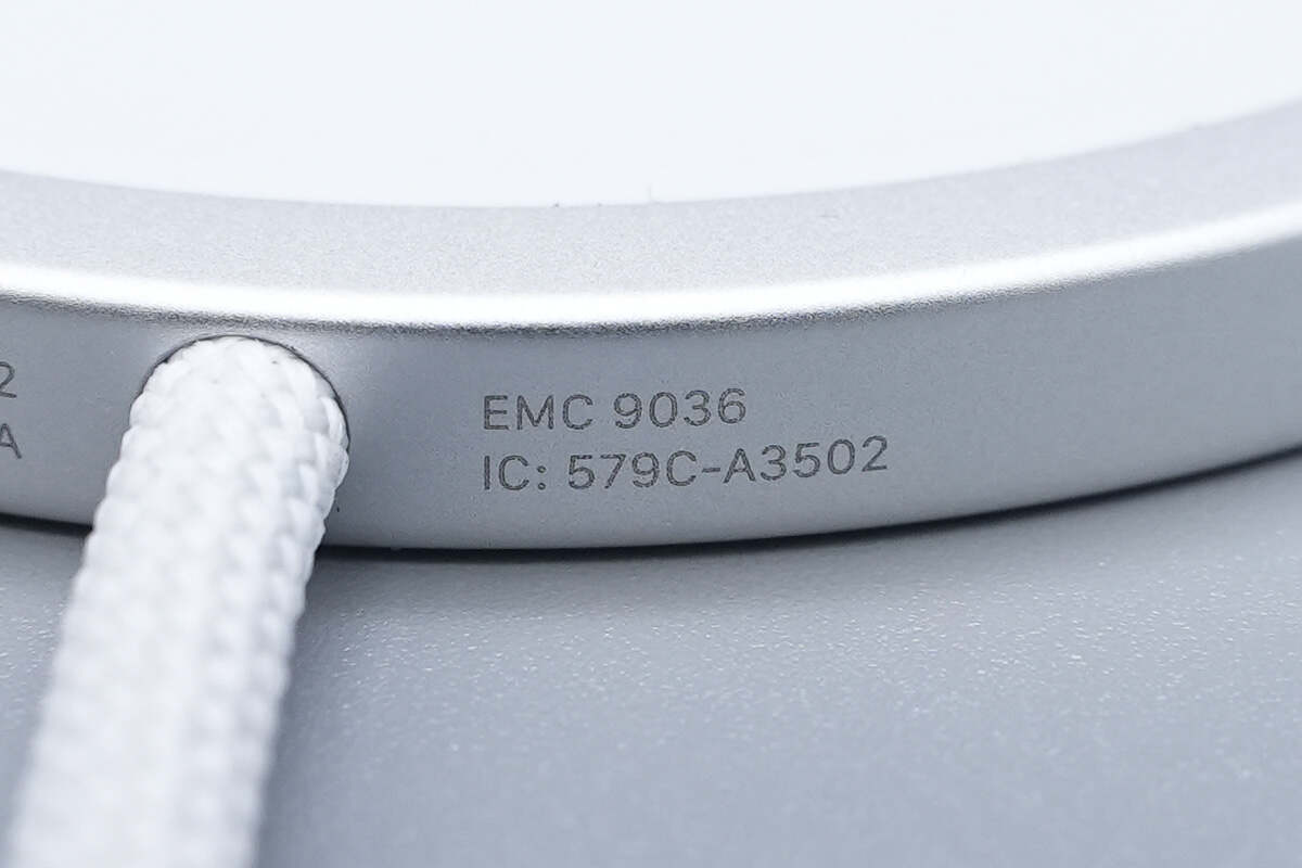
The side has a sticker showing the model number and serial number, and indicates that the product is made in Vietnam.
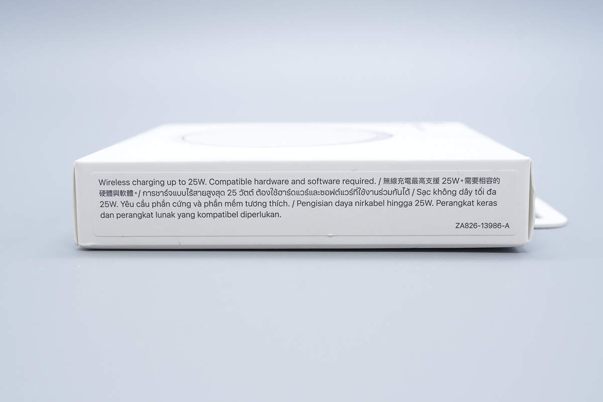
The other side features a sticker with safety and usage warnings.

Open the box.
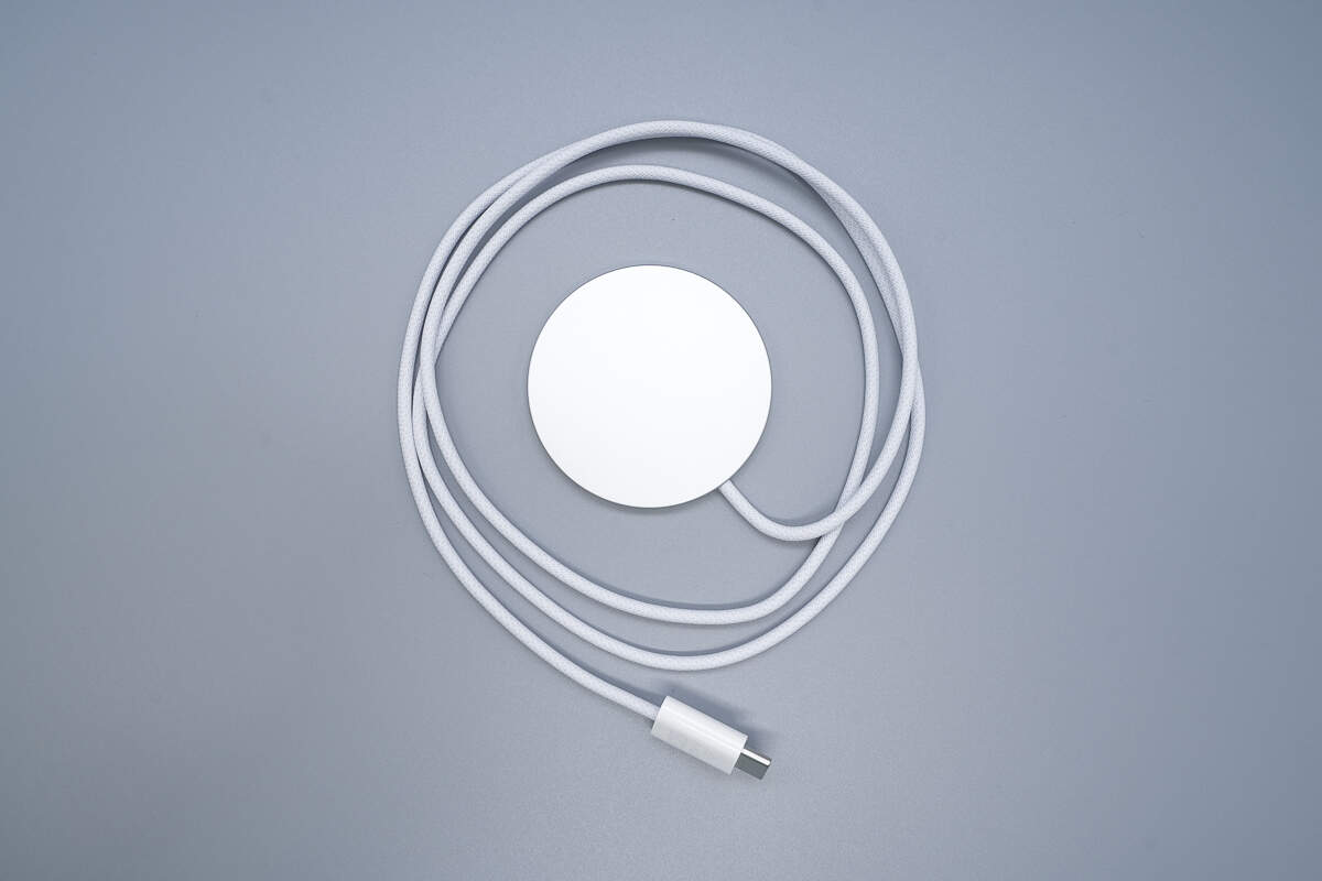
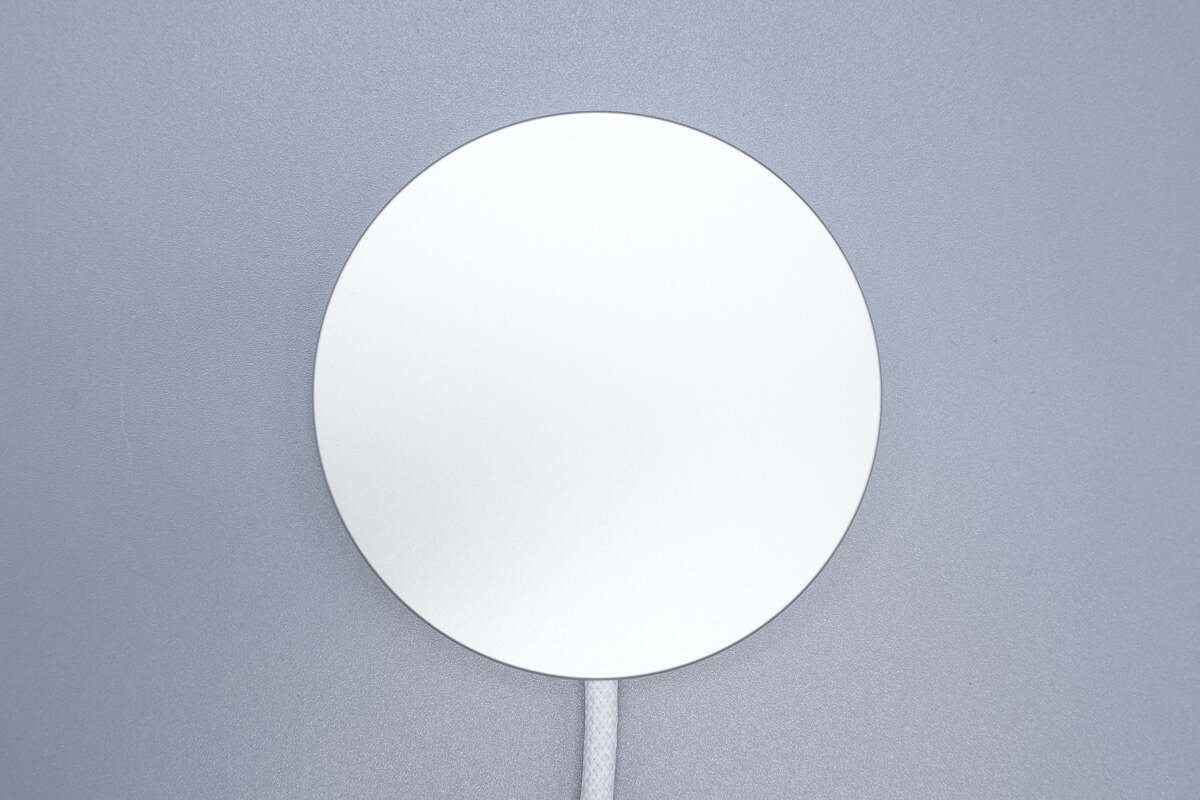
Take out the MagSafe wireless charger from the box.
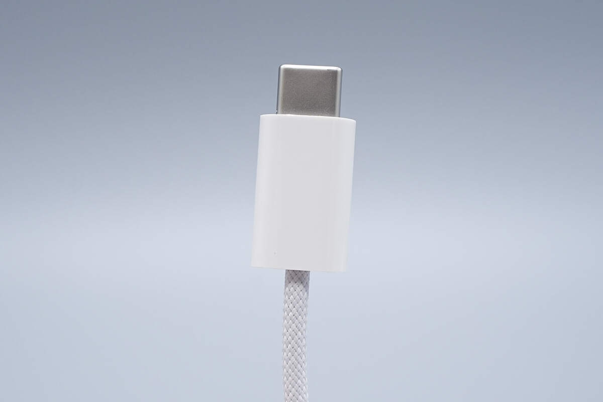
The USB-C connector features a white plastic casing.
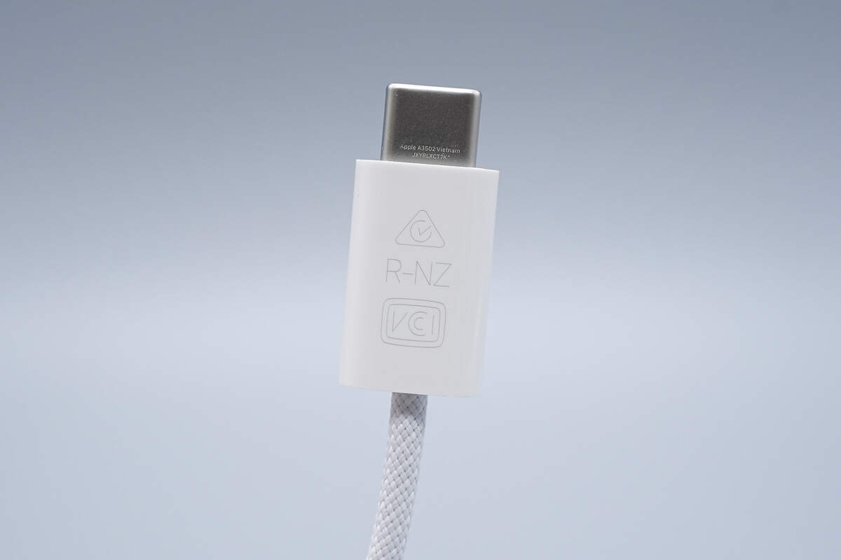
The other side of the plug is printed with the model number and serial number. The casing bears the RCM, R-NZ, and VCCI certification marks.
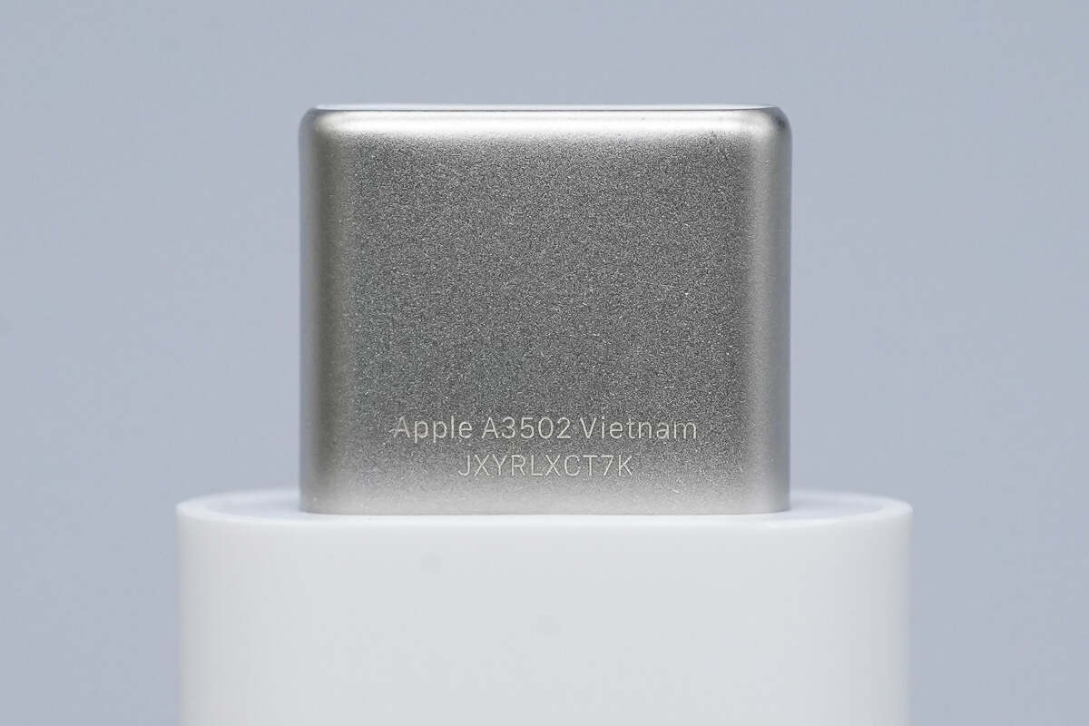
Close-up of the model number, country of manufacture, and serial number information.
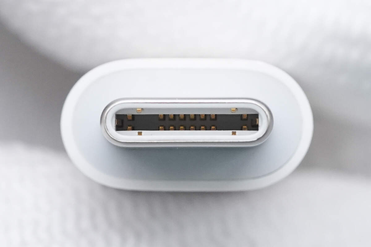
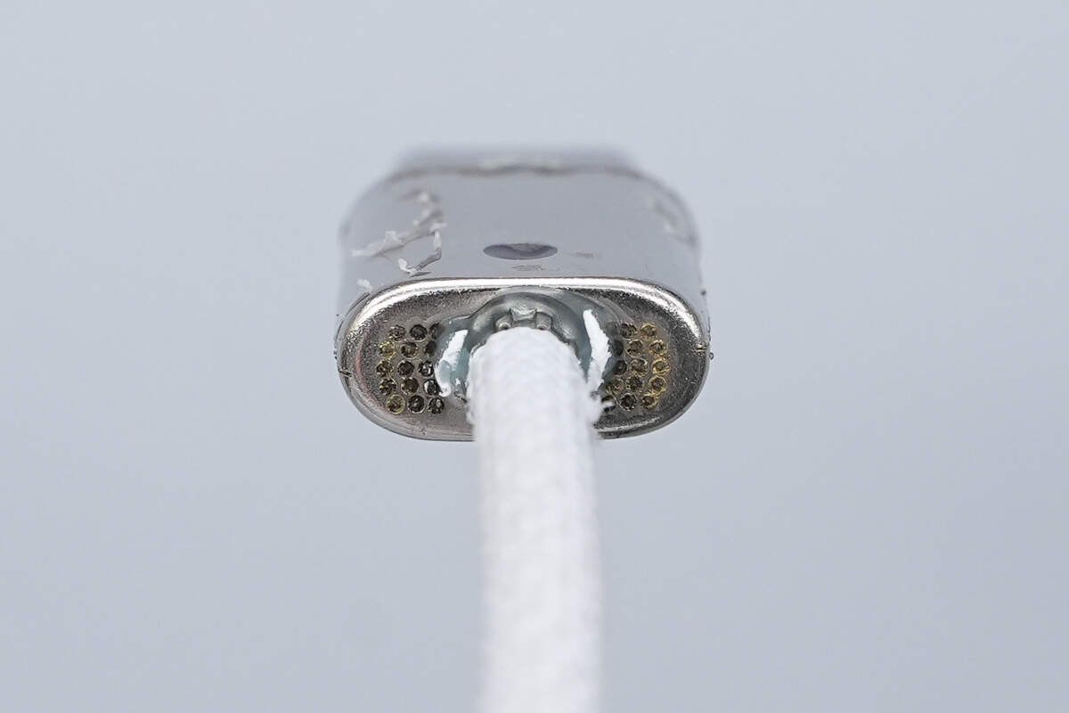
The USB-C connector’s internal pins are gold-plated and feature a non-full pin design.
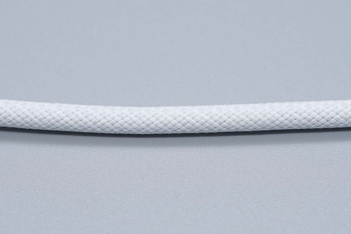
The charger uses a braided cable.
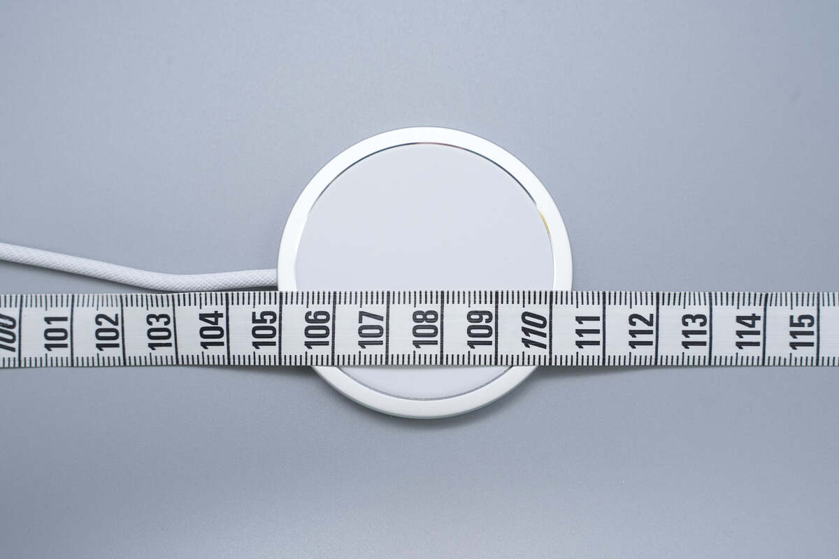
The total length of it is about 110.5 cm (43.5 inches).
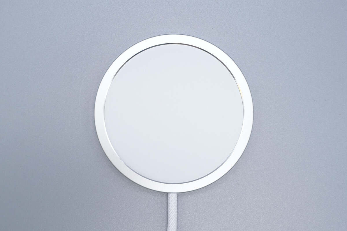
The outer ring is made of aluminum alloy. The center is made of plastic with a smooth, skin-like texture.
The back is made of aluminum alloy.

It supports three input power levels: 5V/3A, 9V/3A, and 15V/3A.
Close-up of the printing on the other side.
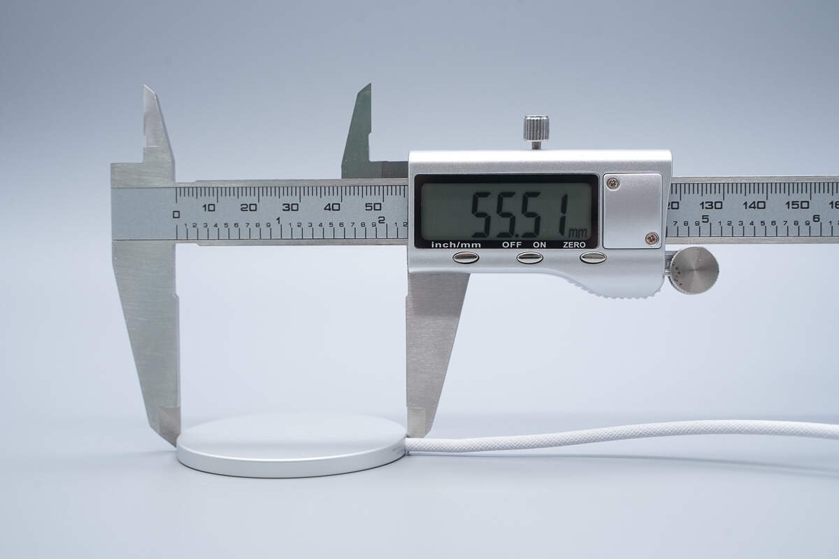
The diameter of the wireless charge panel is about 55.5 mm (2.19 inches).
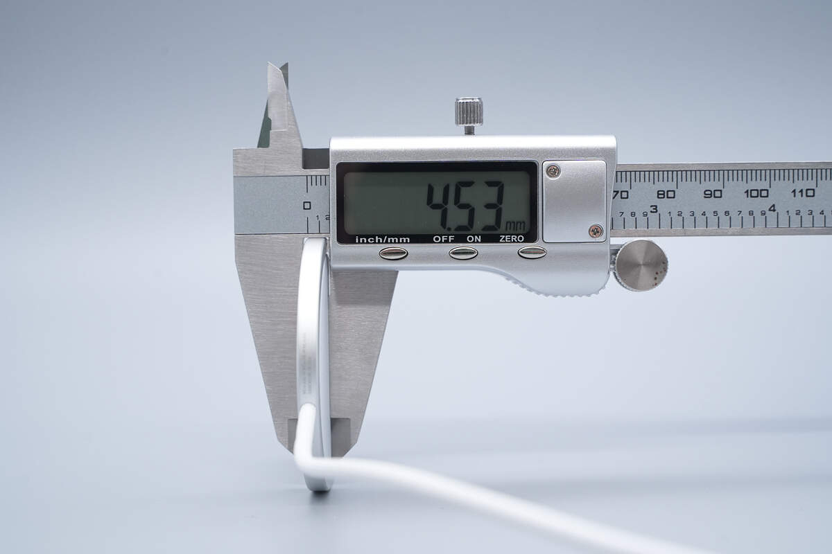
The thickness is about 4.5 mm (0.18 inches).
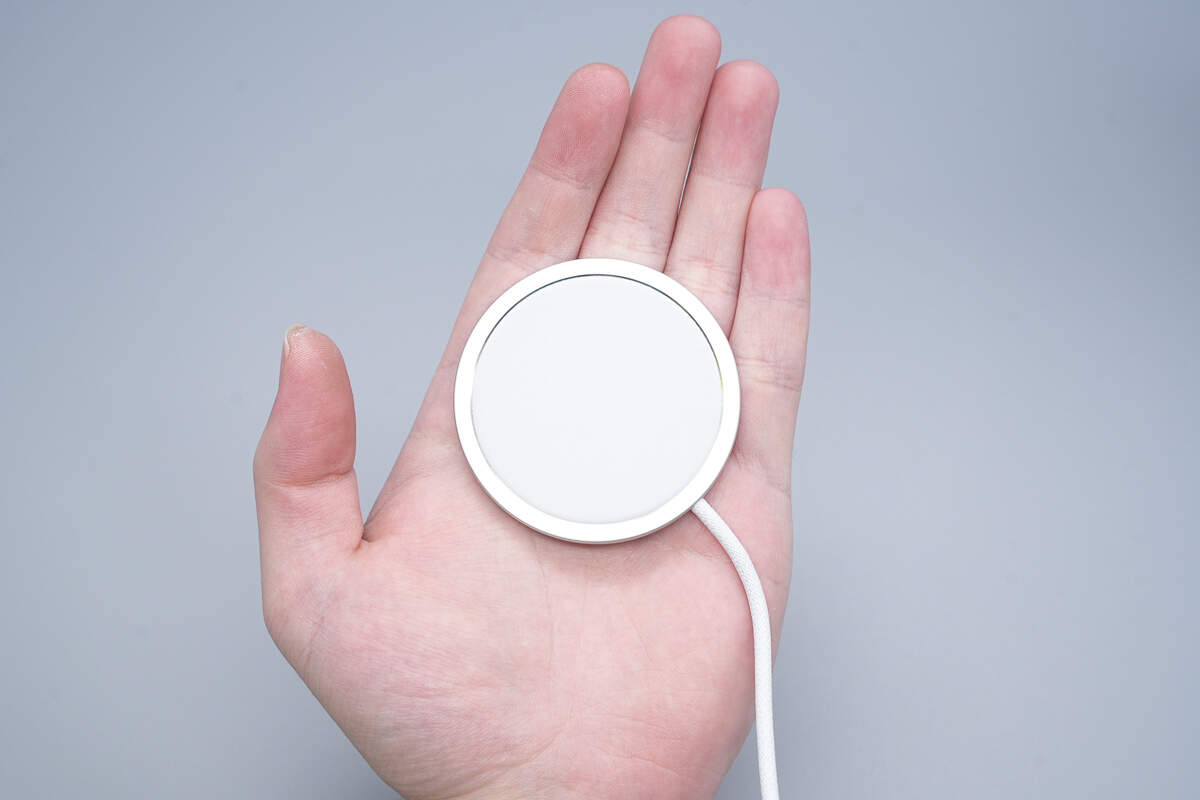
That's how big it is in the hand.
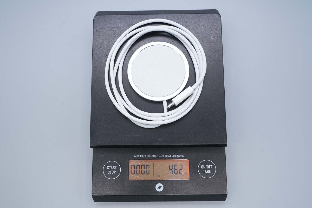
The weight is about 46.2 g (1.63 oz).
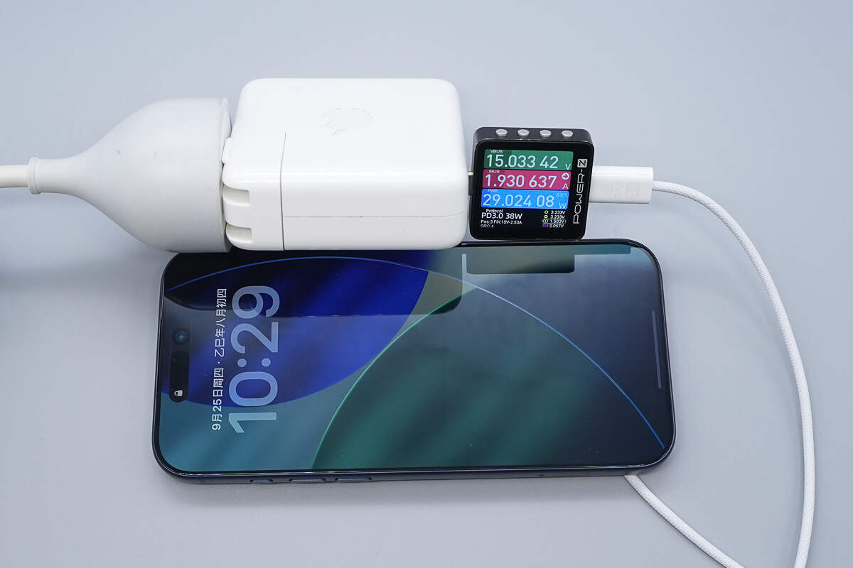
Using an Apple 67W charger paired with it to charge the iPhone 17 Pro Max, the input voltage is 15V, the input current is 1.93A, and the input power is about 29W.
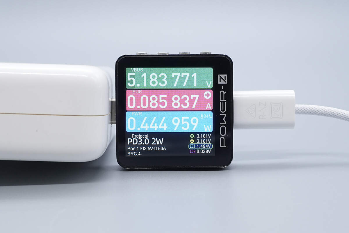
The standby power is about 0.445W.
Teardown
Next, let's start to take it apart and take a look at the internal components.
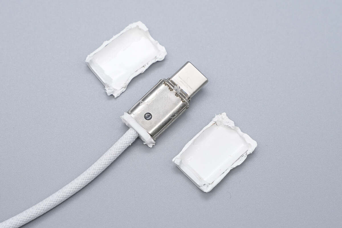
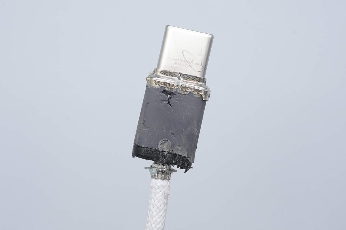
First, use a cutting machine to open the plastic case of the USB-C connector.

The interior is a stainless steel shell fixed by spot welding.
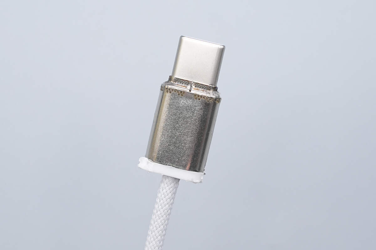
There is no opening on the other side of the shell.
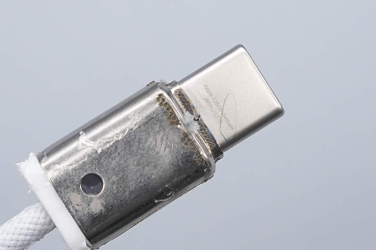
The stainless steel shell and the USB-C plug are fixed by spot-welding.
There are also solder joints at the tail.

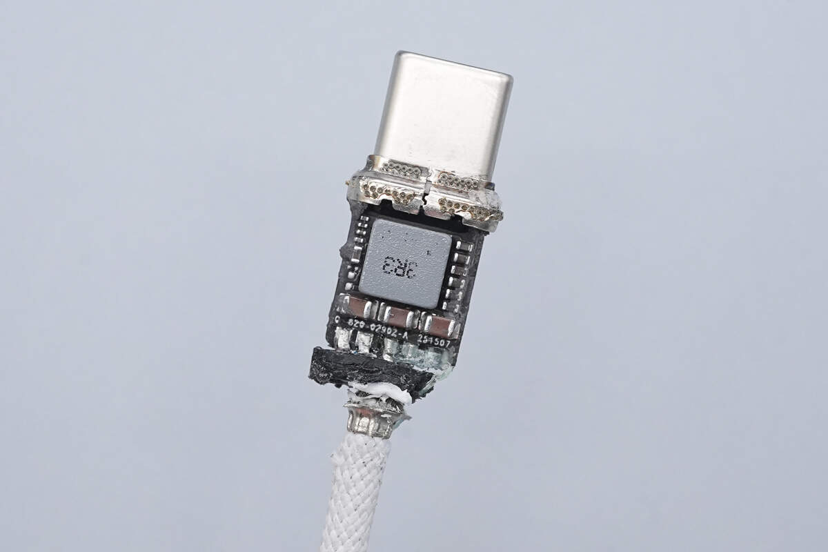
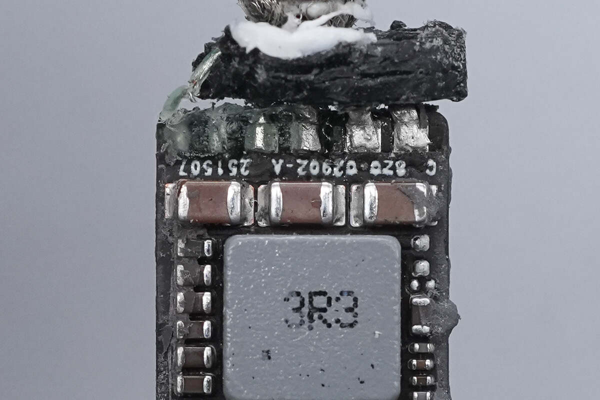
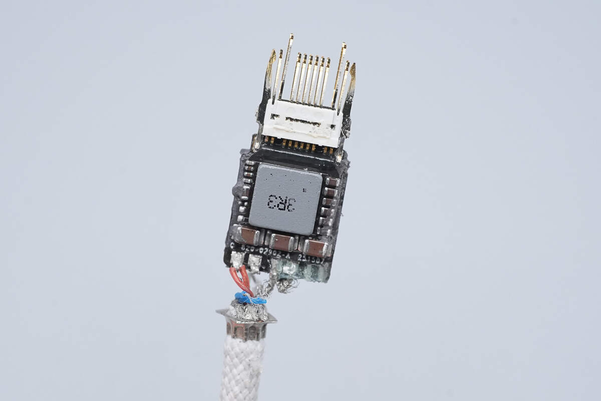
Open the stainless steel shell, and there is a PCBA module inside, and it is filled with glue potting compound. There is a QR code printed on the surface of the inductor.
The other side is filled with potting compound.
After removing the potting compound, one side of the PCBA module reveals an alloy inductor and filtering capacitors.
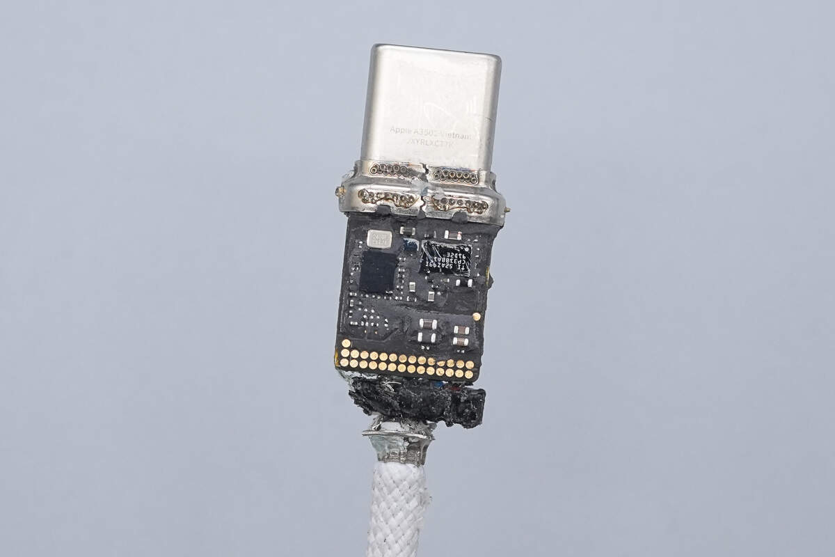
The other side has two chips.
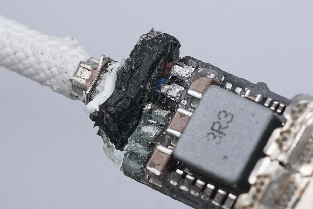
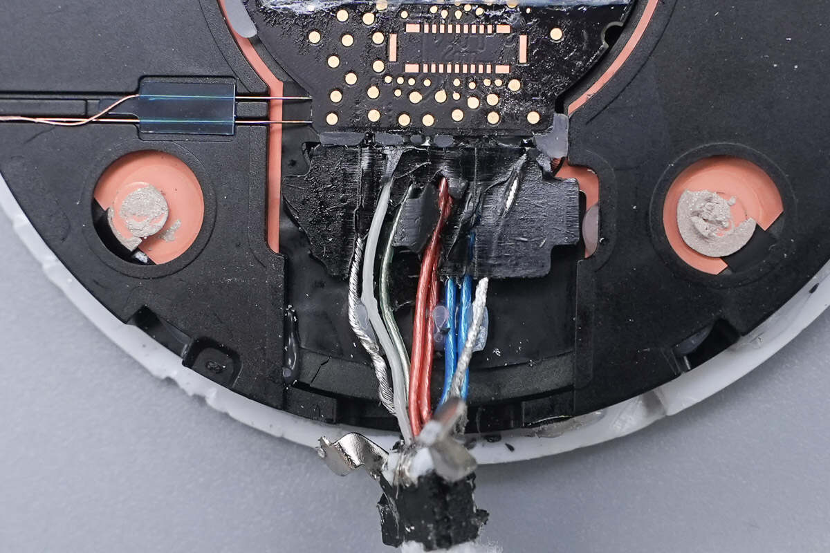
The wires are soldered directly to the PCBA module.

The USB-C interface controller is marked with the code 3GK07.
This is the crystal oscillator used with it.
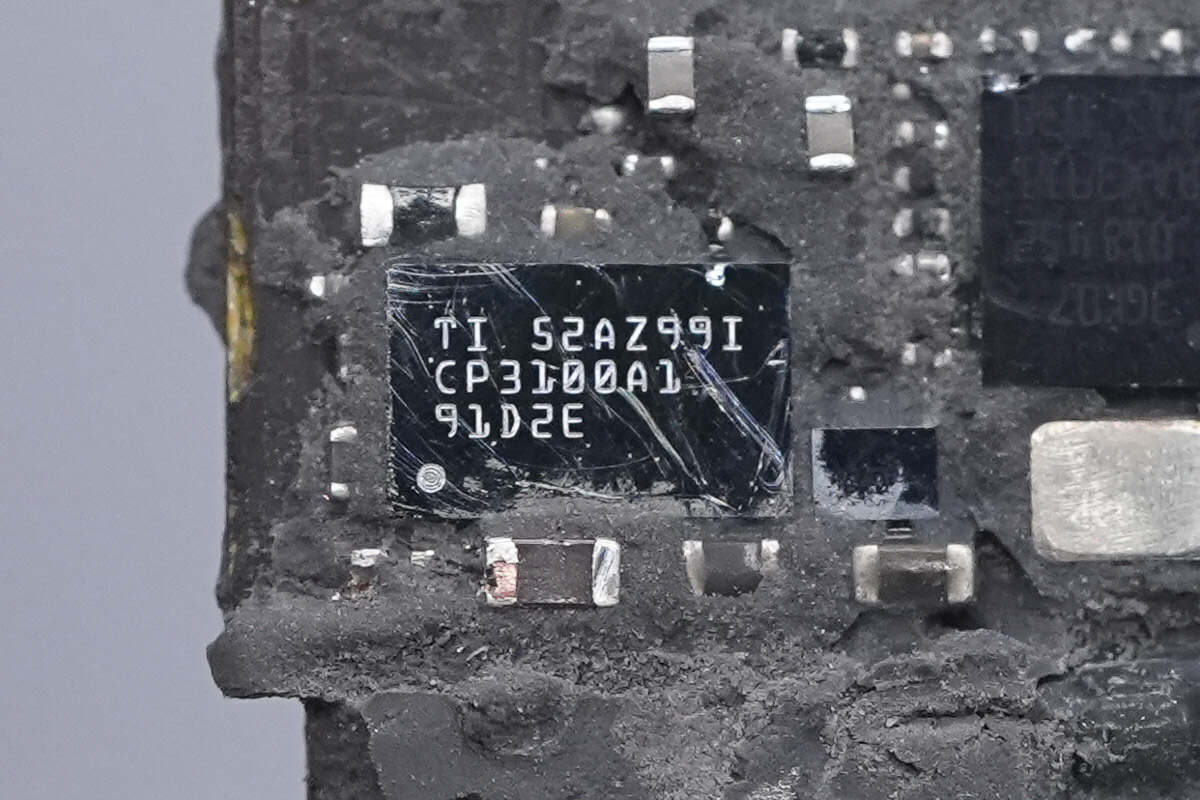
The power conversion chip is marked CP3100A1 and is manufactured by Texas Instruments.
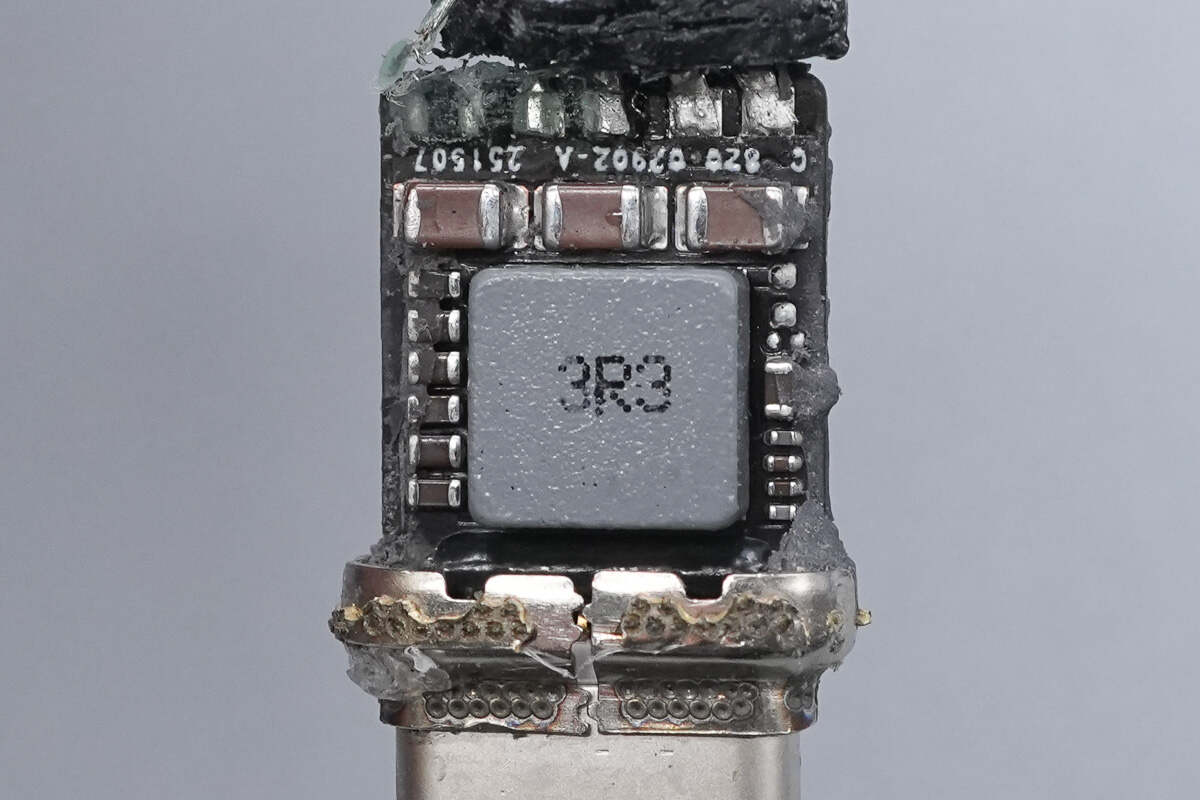
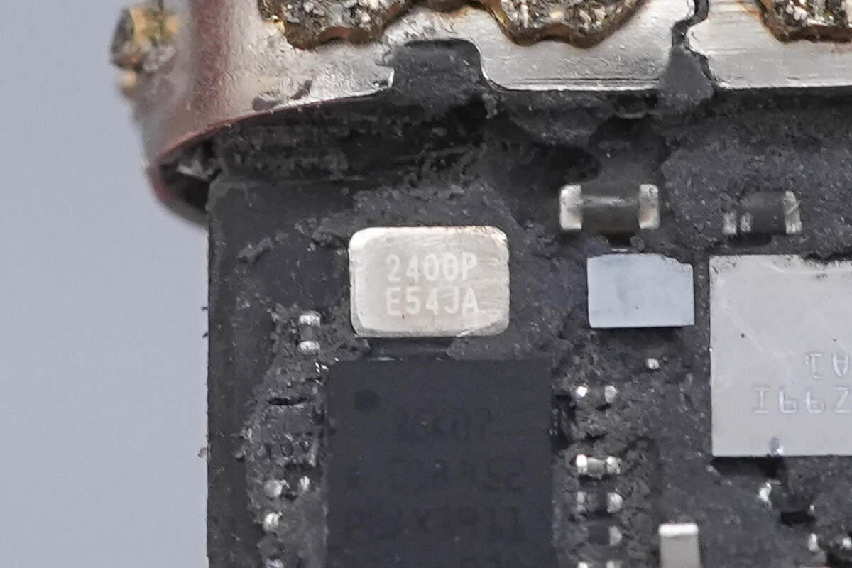
Close-up of the 3.3μH alloy inductor.
Filtering capacitors are located at the rear end of the PCBA module.
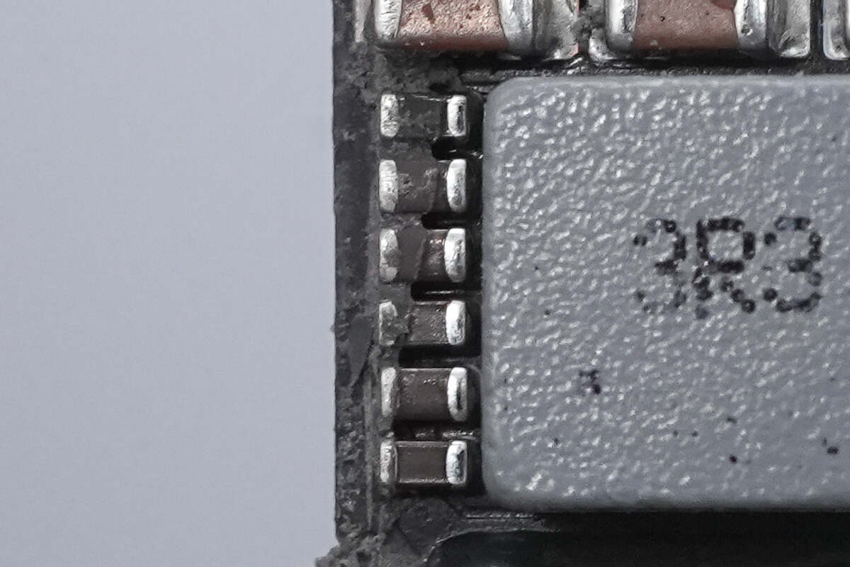
Filtering capacitors are also placed on the side of the PCBA module.

Close-up of an unidentifiable small chip.
Remove the metal shell and plastic frame of the USB-C plug, and you can see the gold-plated pins inside.
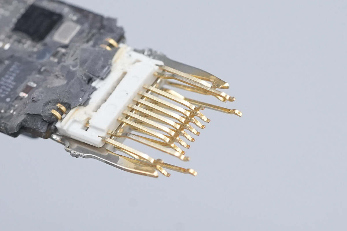
The pins are gold-plated to ensure long-term reliability.
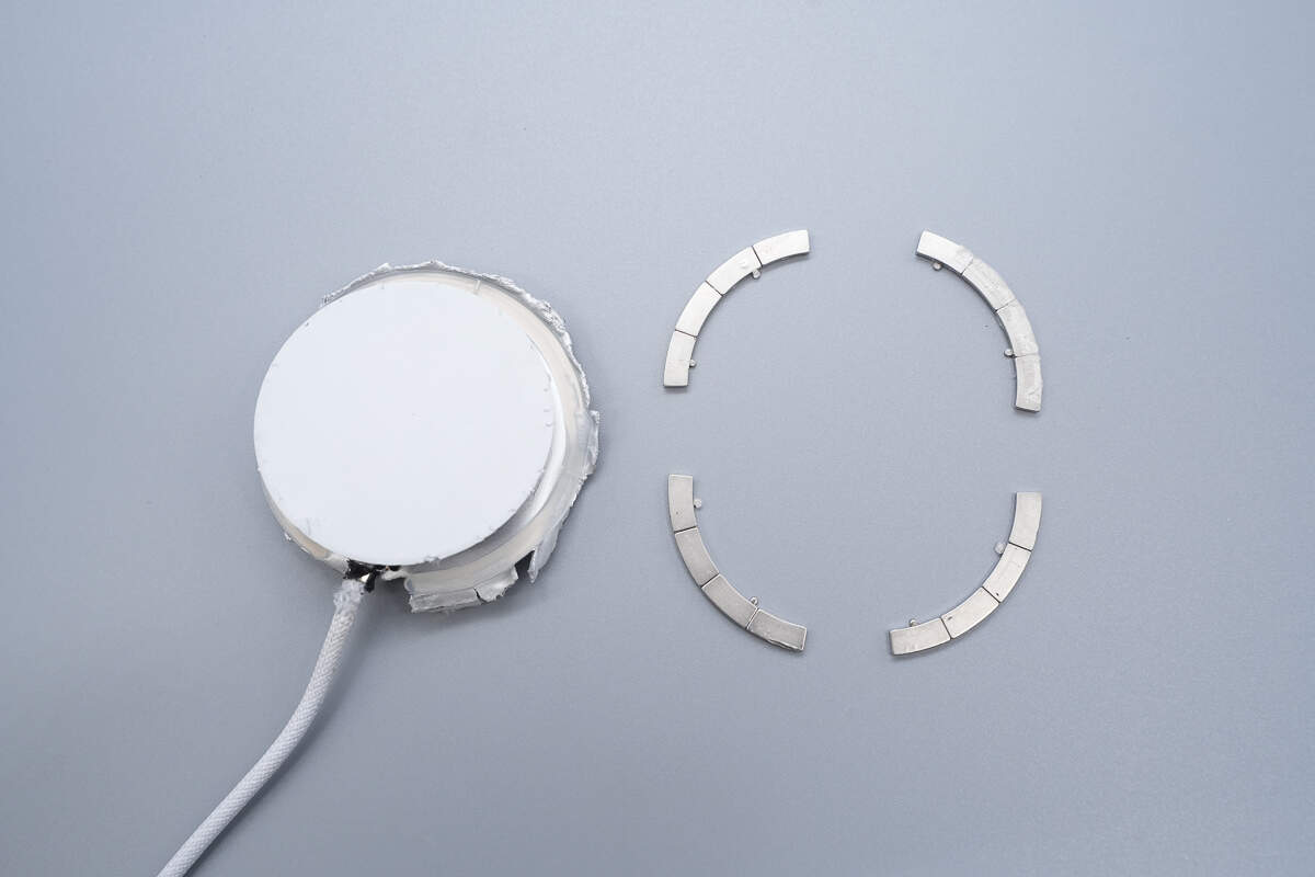
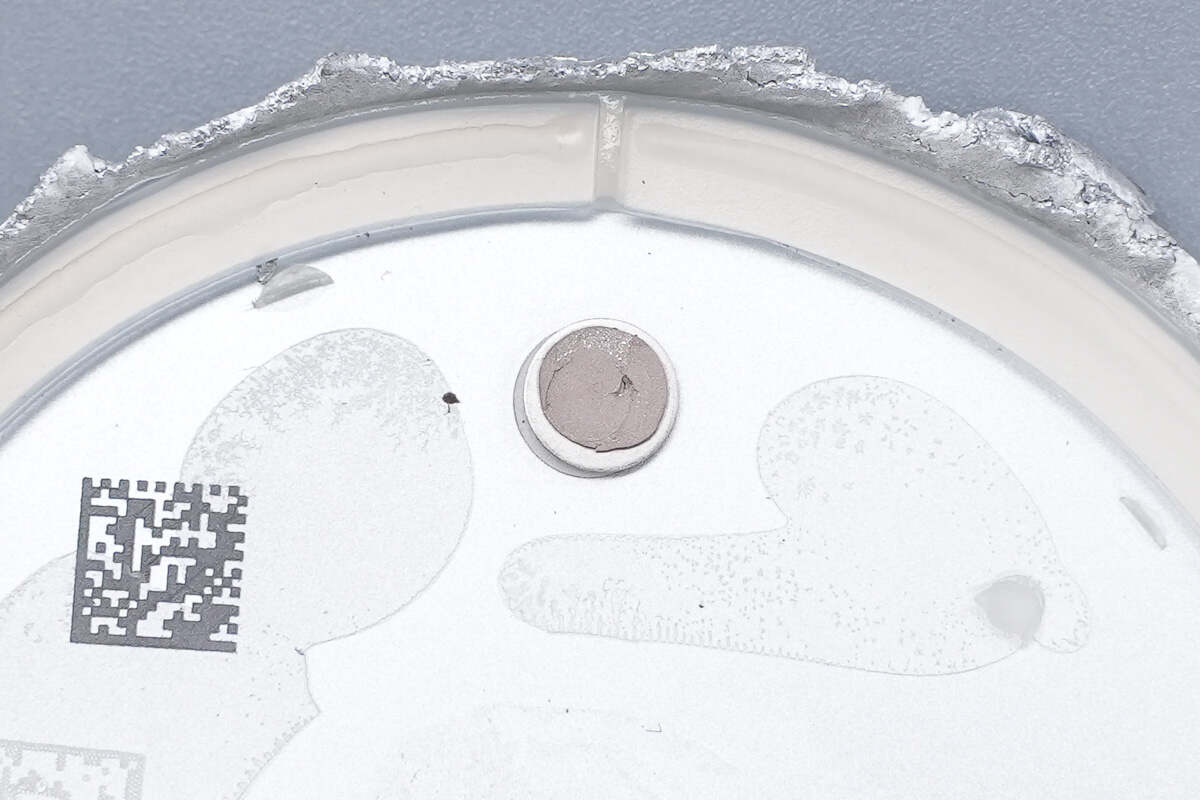
Cut open the aluminum alloy casing of the wireless charging panel. There are four magnets per group, with a total of four groups.
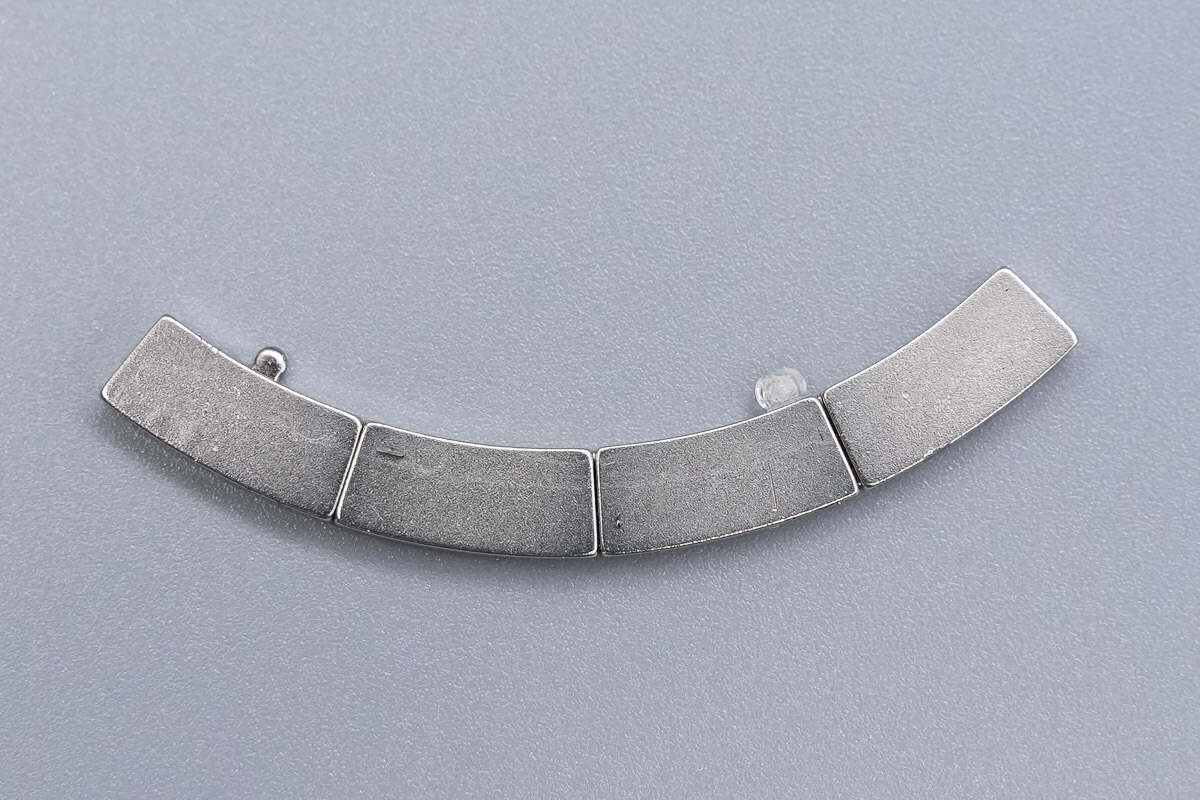
Close-up of the front side of the magnets.
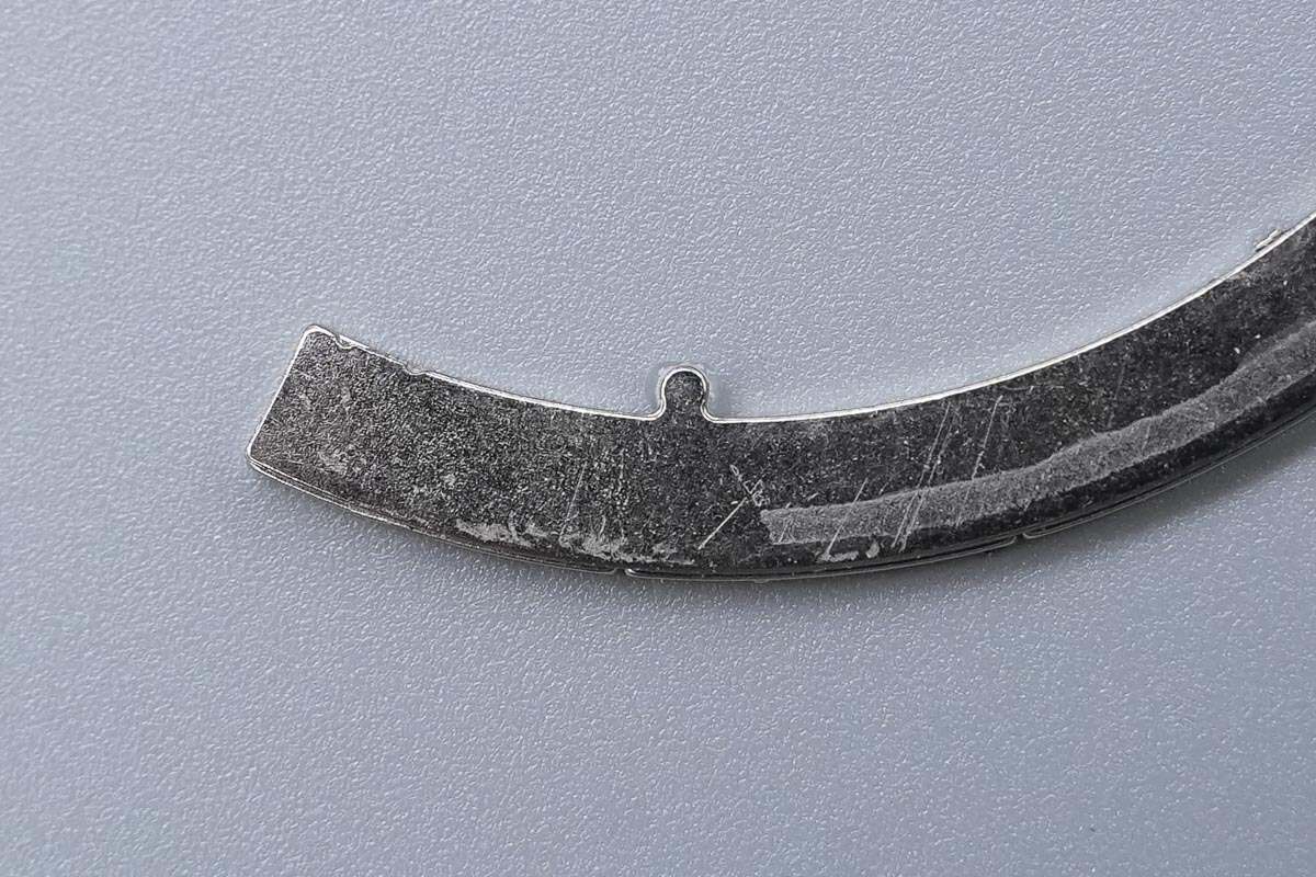
The back side has a mounting plate with positioning pins.
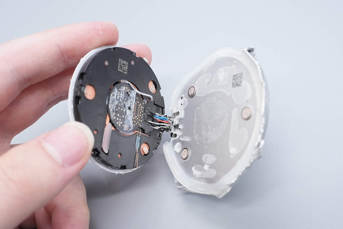
Remove the cover and casing.
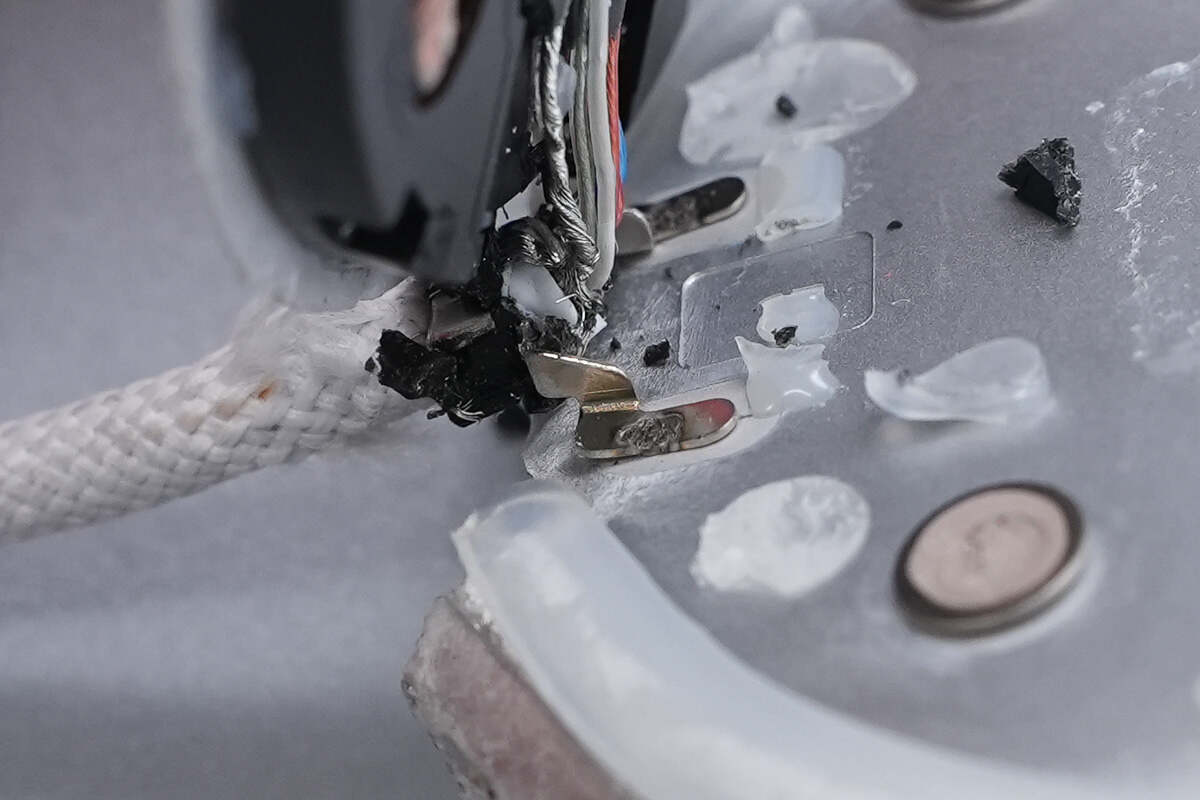
The cable is secured to the casing using clips.
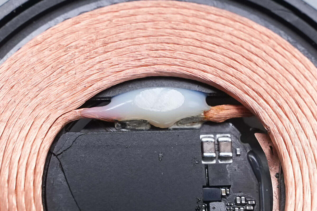
The wires are soldered to the PCBA module.
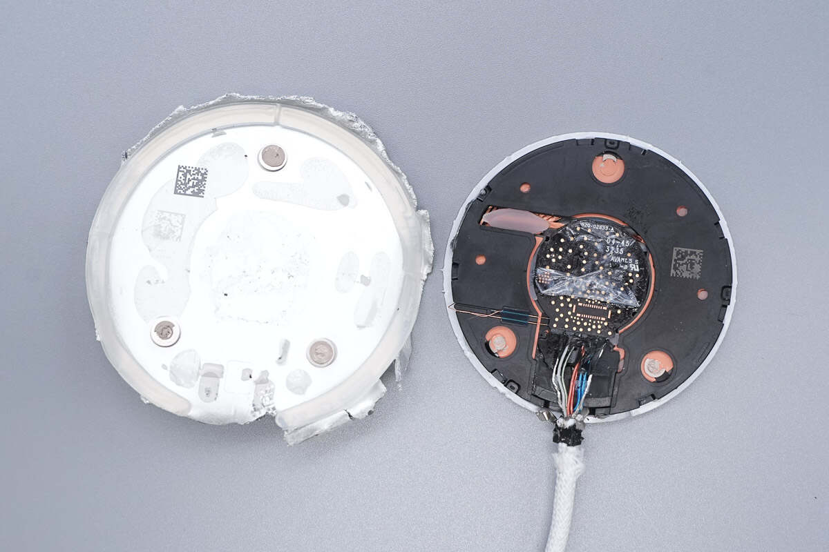
Overview of the casing and the wireless charger panel.
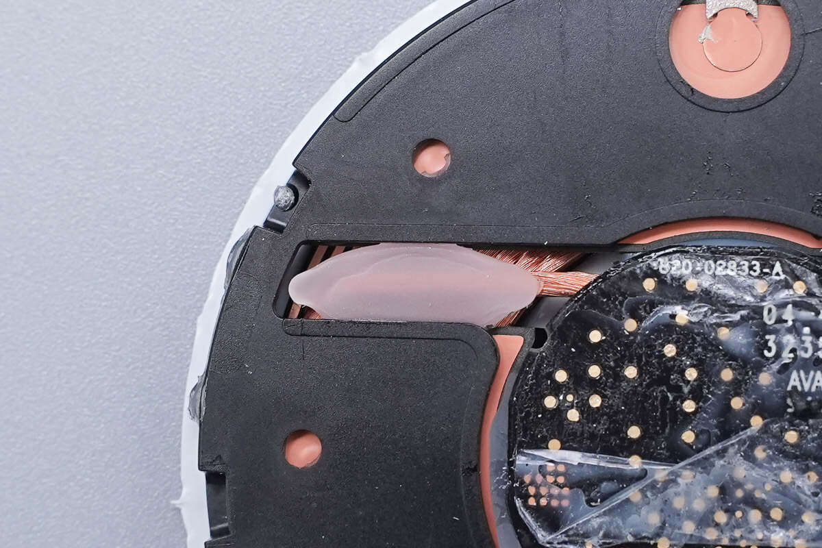
The interior of the casing features raised areas that correspond to the grounding points of the wireless charging panel.
The raised areas are coated with conductive adhesive, and plastic strips are installed along the edge of the casing.
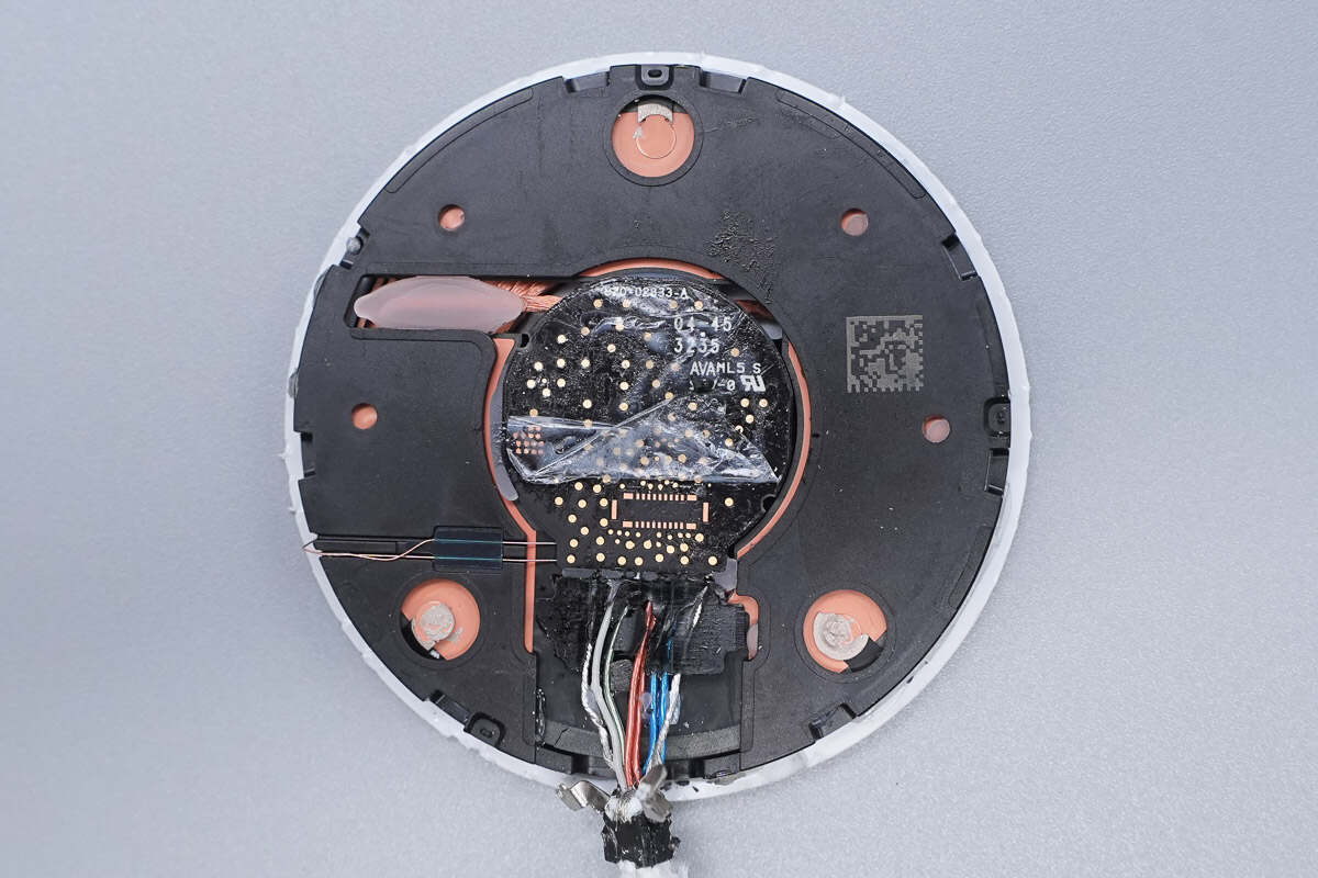
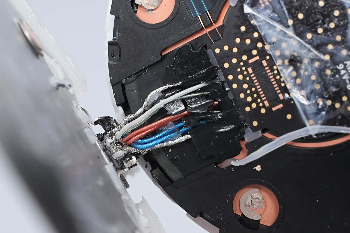
The PCBA module in the center is attached to the casing using double-sided adhesive tape. Black plastic panels along the edges provide insulation and support.
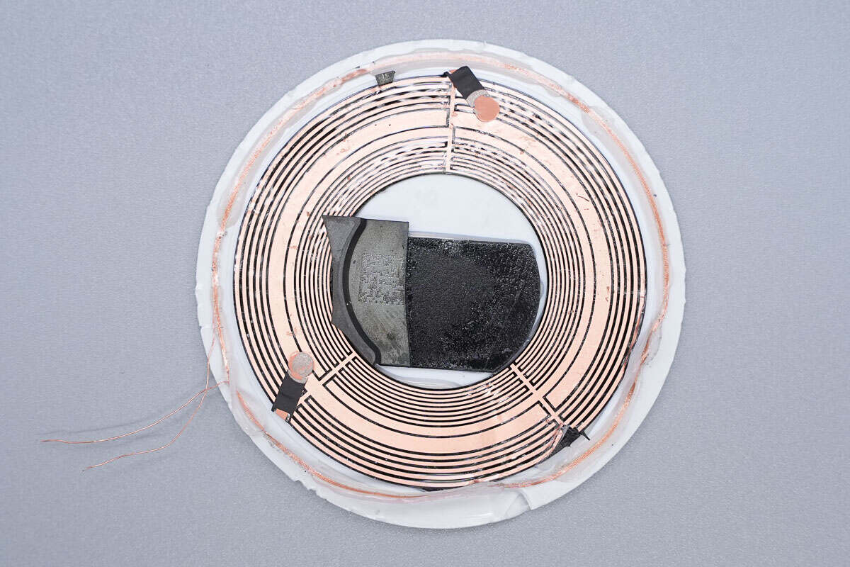
The wireless charging coil is secured with adhesive.

Two thin enameled wires serve as communication coils.
The solder joints of the wires are reinforced with adhesive.
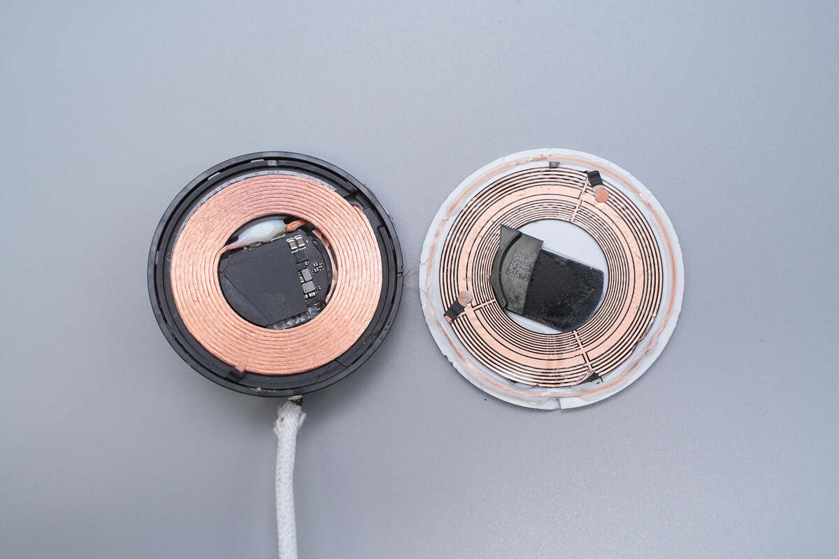
Separate the cover and the wireless charging coil.

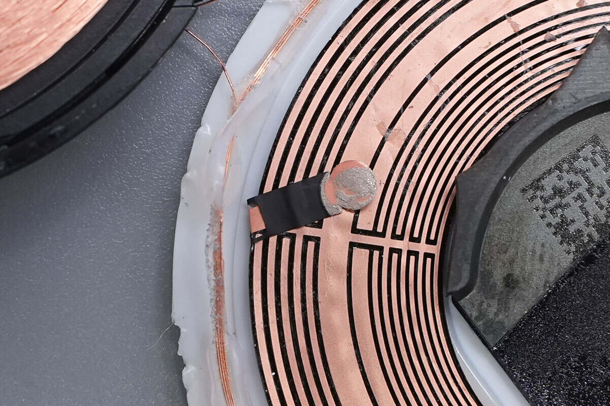
The communication coil is connected using enameled wire.
The shielding layer inside the cover plate is connected to the aluminum alloy casing.
The solder joints of the wireless charging coil are insulated and reinforced with adhesive.
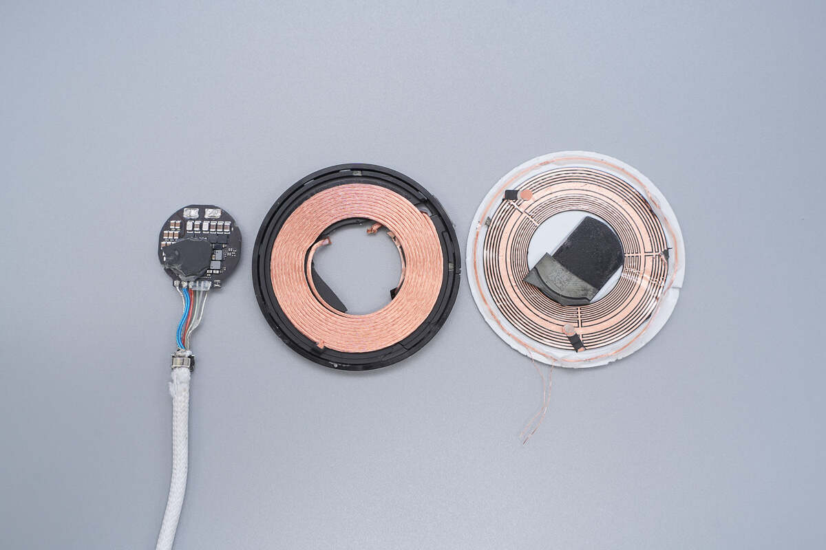
Cut the coil wiring to separate the PCBA module from the wireless charging coil.

There is a magnetic shielding sheet at the bottom of the wireless charging coil.
Close-up of the shielding layer inside the cover plate.
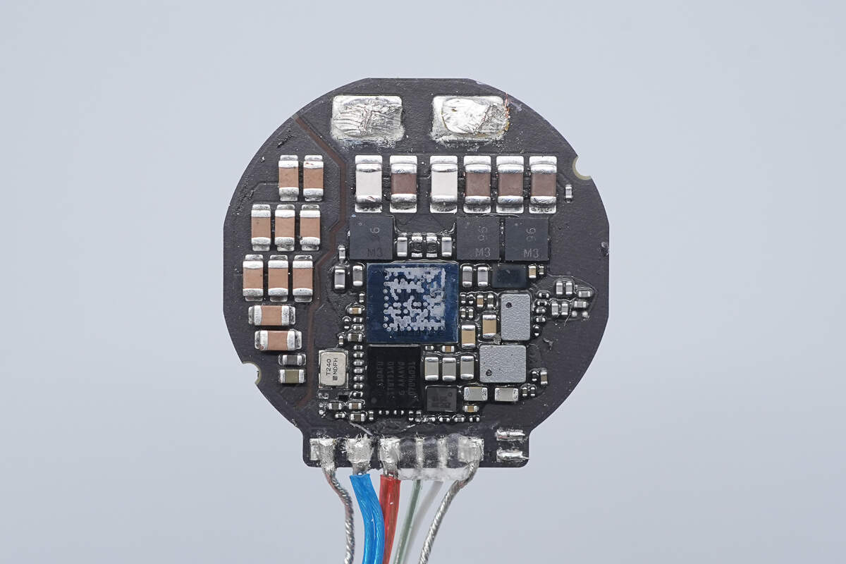
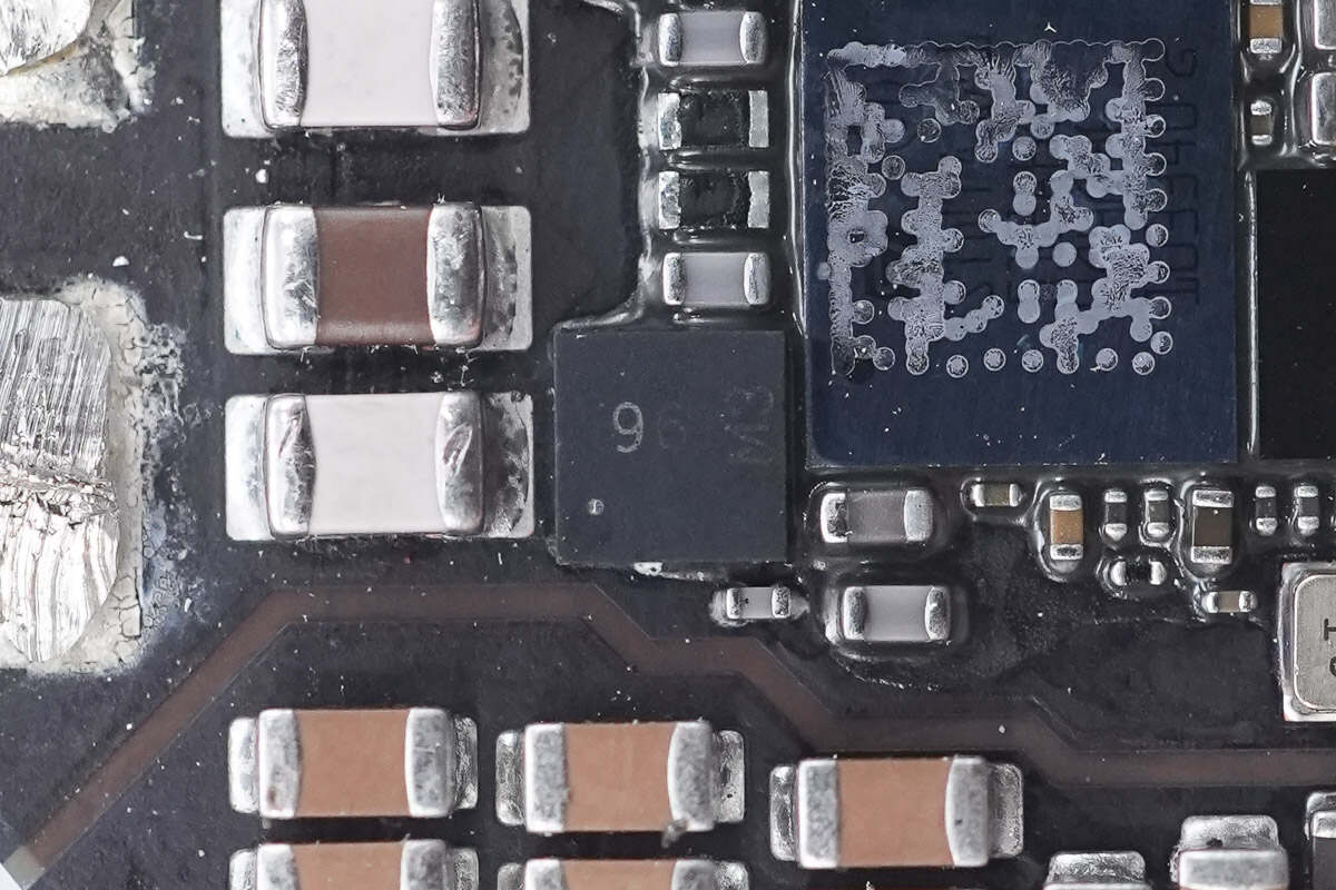
The front side of the PCBA module features filtering capacitors, resonant capacitors, MOSFETs, the wireless charging power stage chip, the wireless charging controller, and memory.
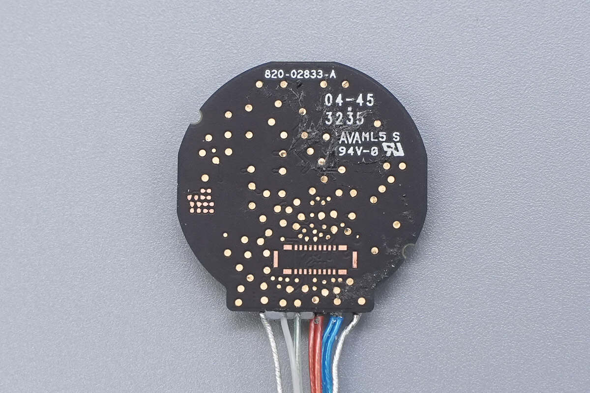
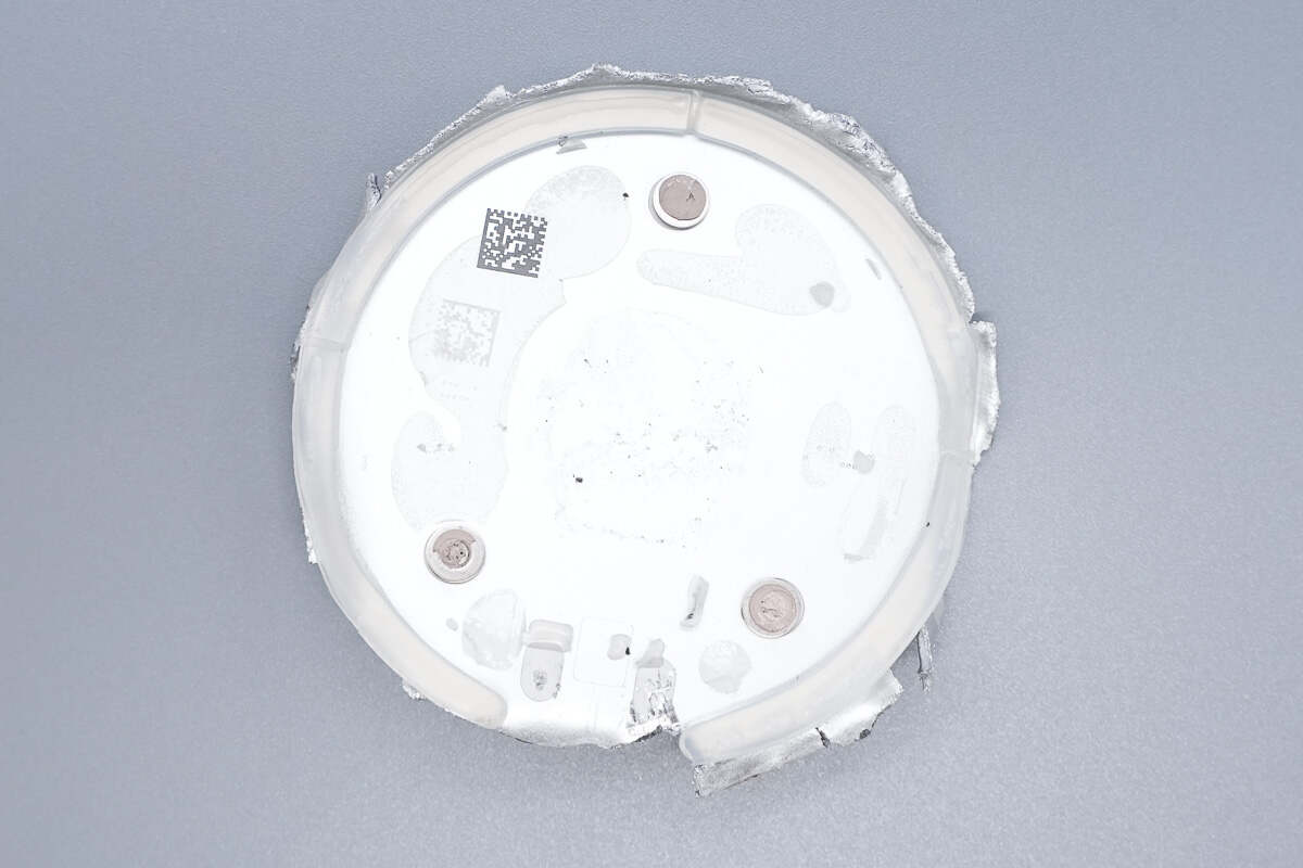
There are no components on the back side.
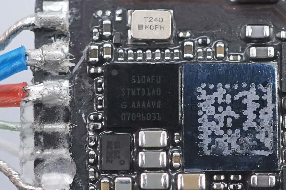
The wireless charging master control chip is from STMicroelectronics, marked with STWTD1A0.

Close-up of the external clock crystal oscillator.
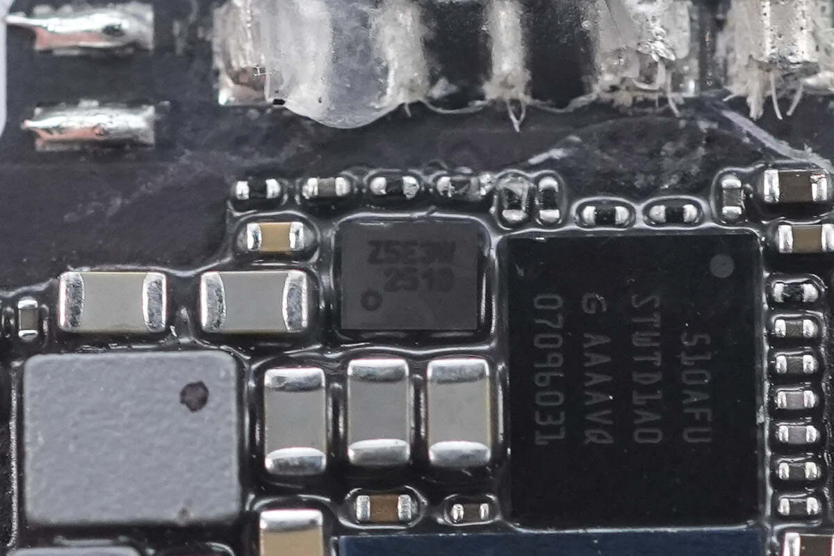
The memory chip is marked with Z5E3W.

The surface of the wireless charging chip is printed with a QR code.
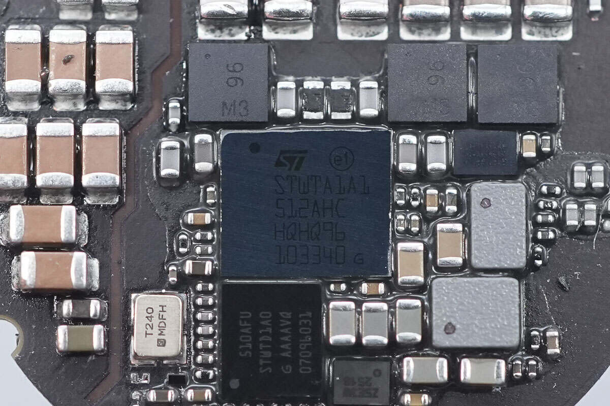
After removing the surface coating, the chip is marked with STWTA1A1.
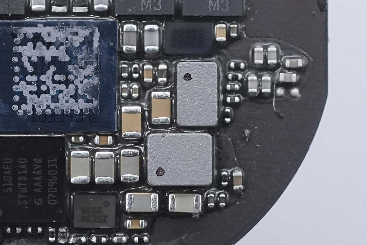
Close-up of the two external alloy inductors.
Close-up of the external MLCC filtering capacitors.

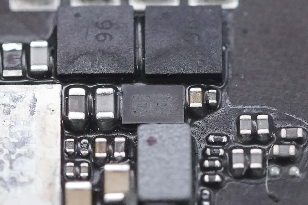
The MOSFET used for switching the resonant capacitors is from DIODES, marked with "96," model DMT12H065LFDF. It is an NMOS with a voltage rating of 115V and an on-resistance of 65mΩ, packaged in a U-DFN2020-6 form factor.
The other MOSFET has the same model.

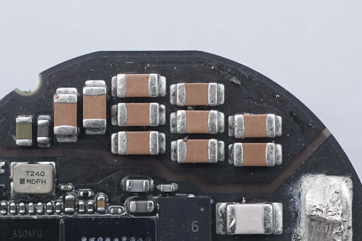
Close-up of the SMD resonant capacitors.
Close-up of an unidentifiable chip.

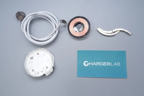
Well, those are all components of the new MagSafe Charger.
Summary of ChargerLAB
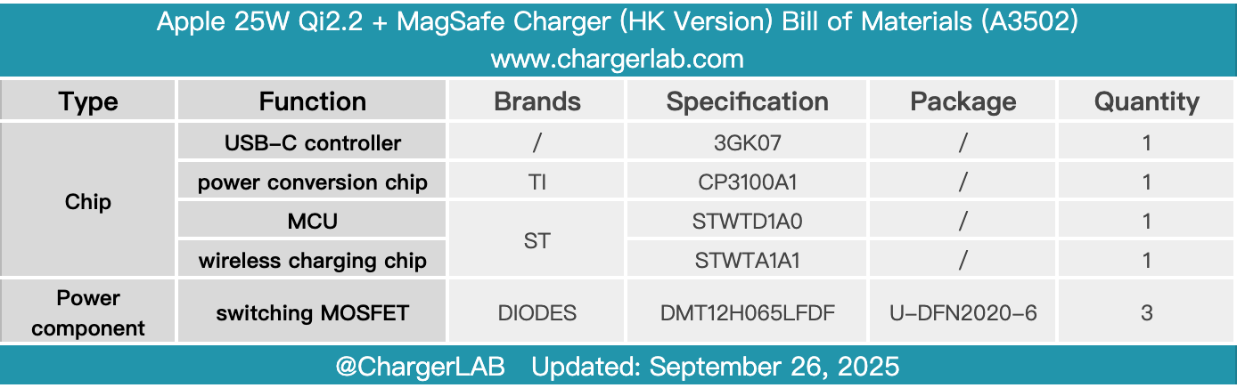
Here is the component list of the Apple 25W Qi2.2 + MagSafe Charger A3502 (HK Version) for your convenience.
It continues the design of separating the power conversion circuit from the wireless charging circuit, which helps disperse heat and extend the duration of high-power output. The use of a braided cable enhances durability.
After taking it apart, we found that the USB-C plug houses a USB-C controller and a Texas Instruments CP3100A1 power chip. Inside the wireless charger panel, there is an STMicro STWTD1A0 MCU and an STWTA1A1 wireless charging chip, along with three DIODES DMT12H065LFD MOSFETs used for resonant capacitors switching.
The USB-C plug is spot-welded and secured with a stainless steel sleeve. Inside, it houses a PCBA module filled with thermal adhesive. The wireless charging panel features an aluminum alloy casing, with the PCBA module attached to the casing using double-sided adhesive tape. Multiple measures are implemented to enhance heat dissipation and reduce temperature rise during high-power wireless charging.
Related Articles:
1. Teardown of EcoFlow RAPID 170W 25000mAh Power Bank (EF-HB-002)
2. Teardown of MEAN WELL 1500W Switching Power Supply (SE-1500-24)
3. Teardown of BricBloc 67W All-in-One Charger