Introduction
Not long ago, ChargerLAB got a charging station A91B2 from the well-known brand ANKER. In addition to two AC slots, it is also equipped with six USB ports, and four of the USB-C ports support 140W PD3.1 fast charging, with a total output power of up to 240W.
Not only that, it also innovatively integrates AC and DC power supplies into the included power adapter. This makes its design different from similar products on the market. Next, take its 253W power adapter apart to see its internal components and structure.
Product Appearance
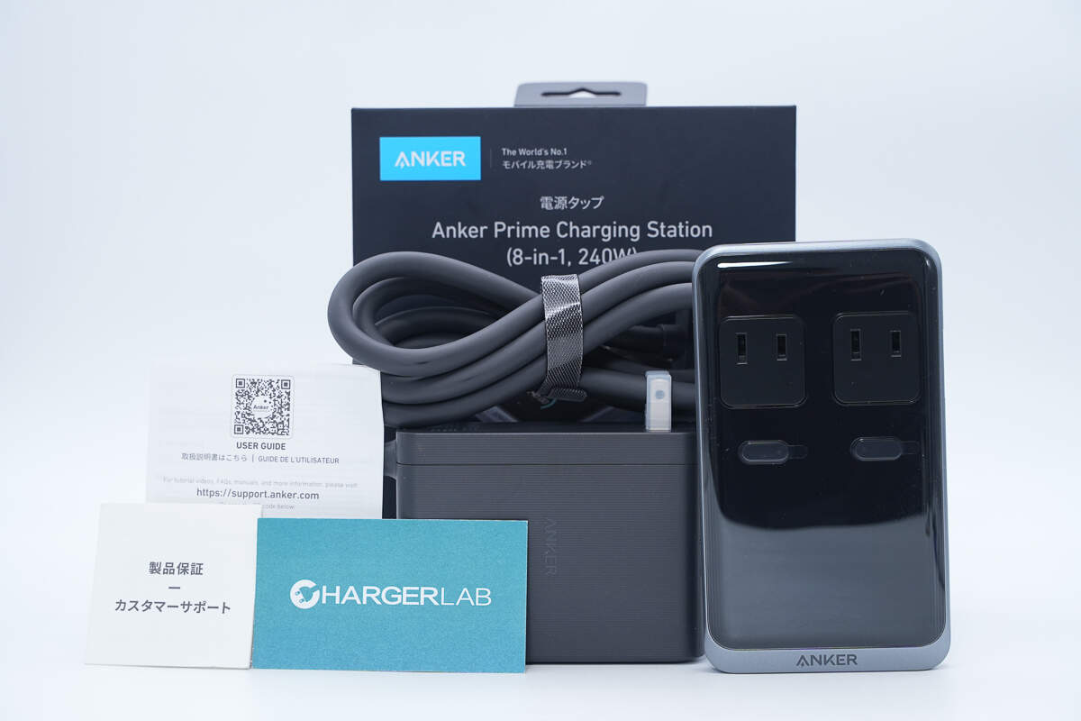
The packaging of the ANKER 240W 8-in-1 charging station contains the charging station, the 253W power adapter, and some documents.
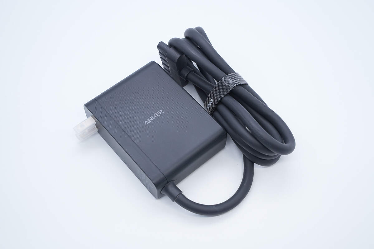
The design style of this power adapter is simple. The DC output end comes with a cable, but the connector is a special plug.
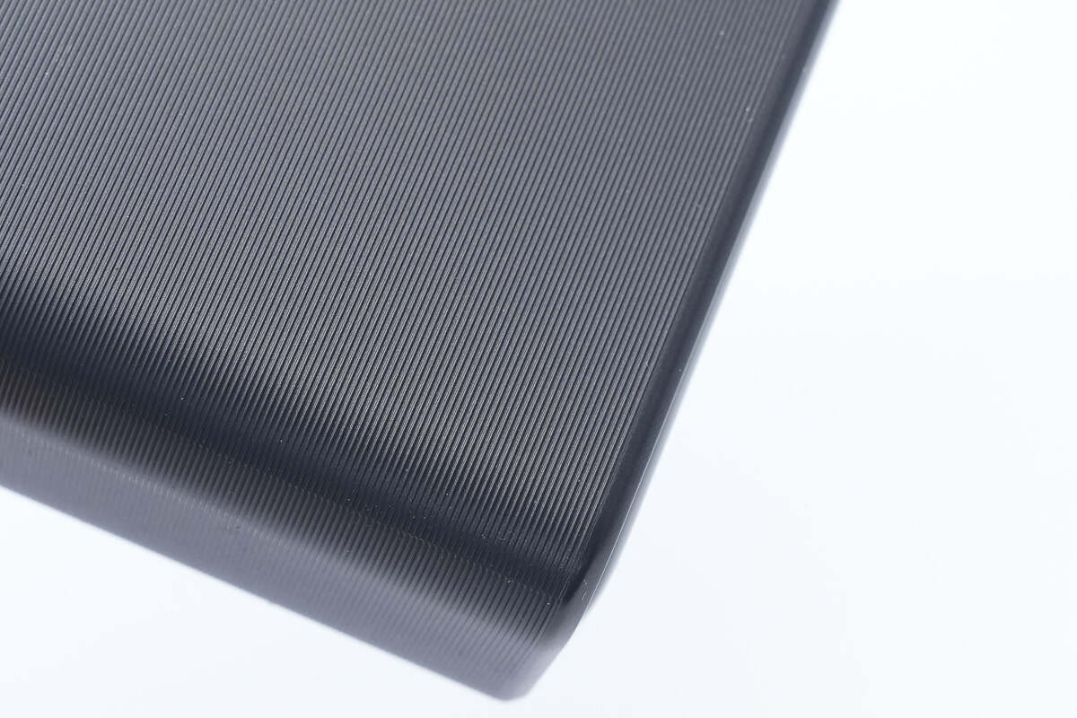
The power adapter has a bumpy texture on its surface.
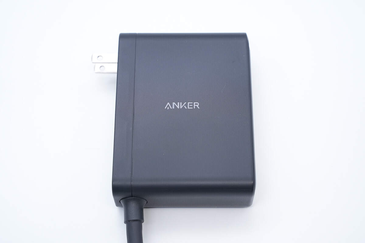
ANKER is engraved in the center of the front.
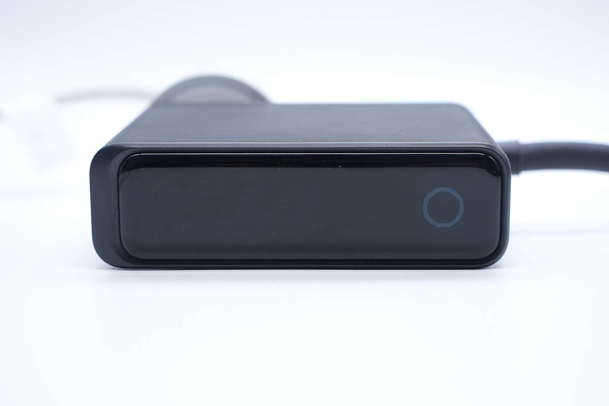
The top is decorated with a bright panel, and there is a light ring on the side close to the output end to indicate whether it is powered on.
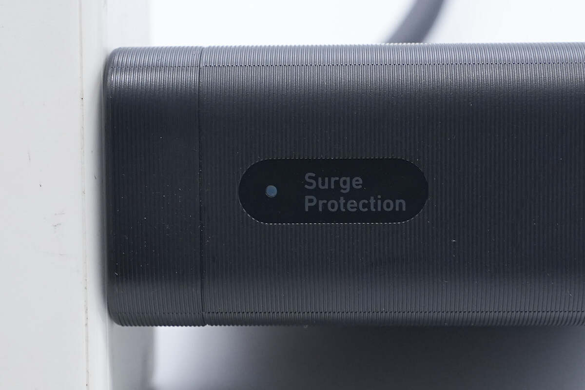
It also has a surge protection indicator light on the front.
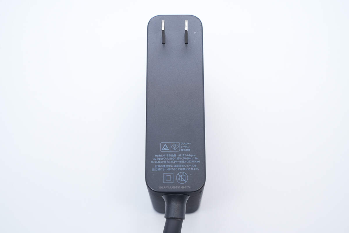
The spec info is printed on the bottom.
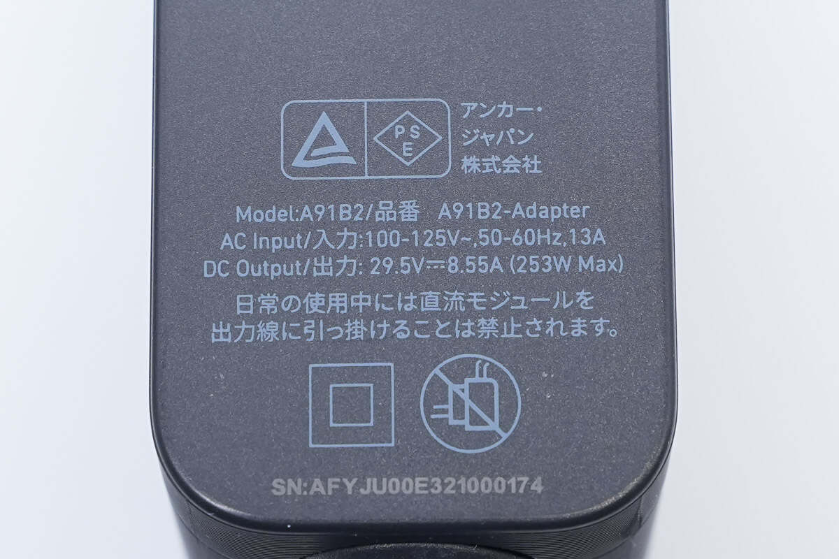
Model: A91B2-Adapter
AC Input: 100-125V~50/60Hz 13A
DC Output: 29.5V8.55A (253W Max)
It has passed PSE certification.
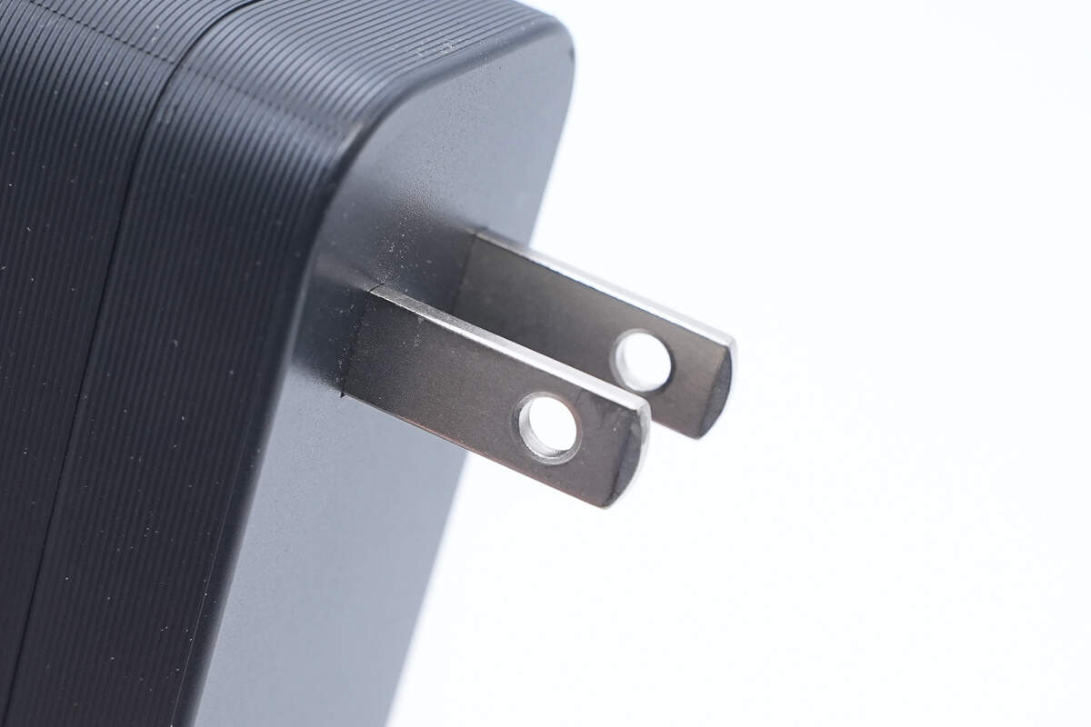
It adopts fixed input pins.
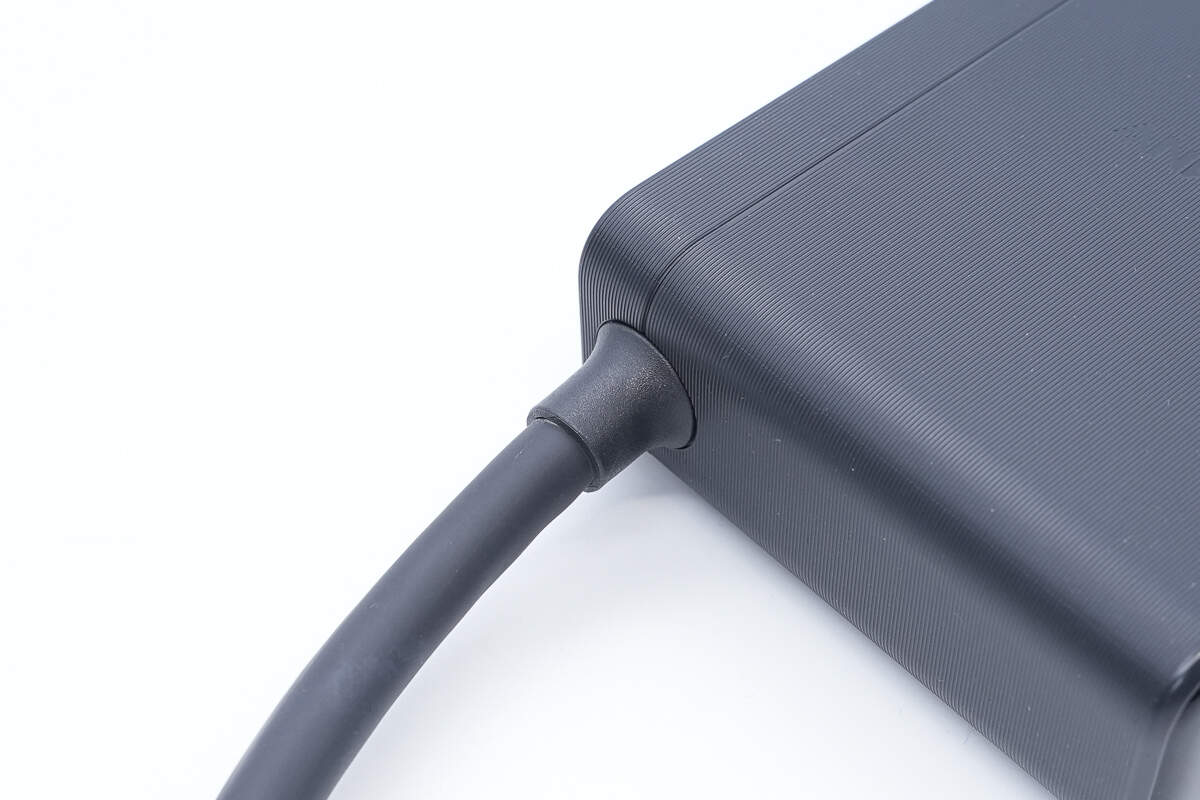
The connection between the body and the cable is protected by a rubber sleeve.
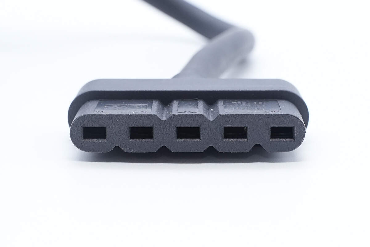
The output connector adopts a special design, which can provide 29.5V8.55A DC output and AC output.
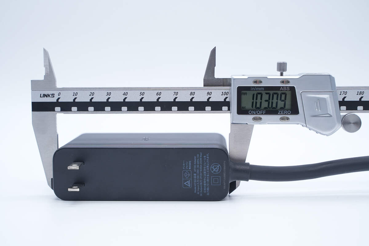
The length of the power adapter is about 103.09 mm (4.059 inches).
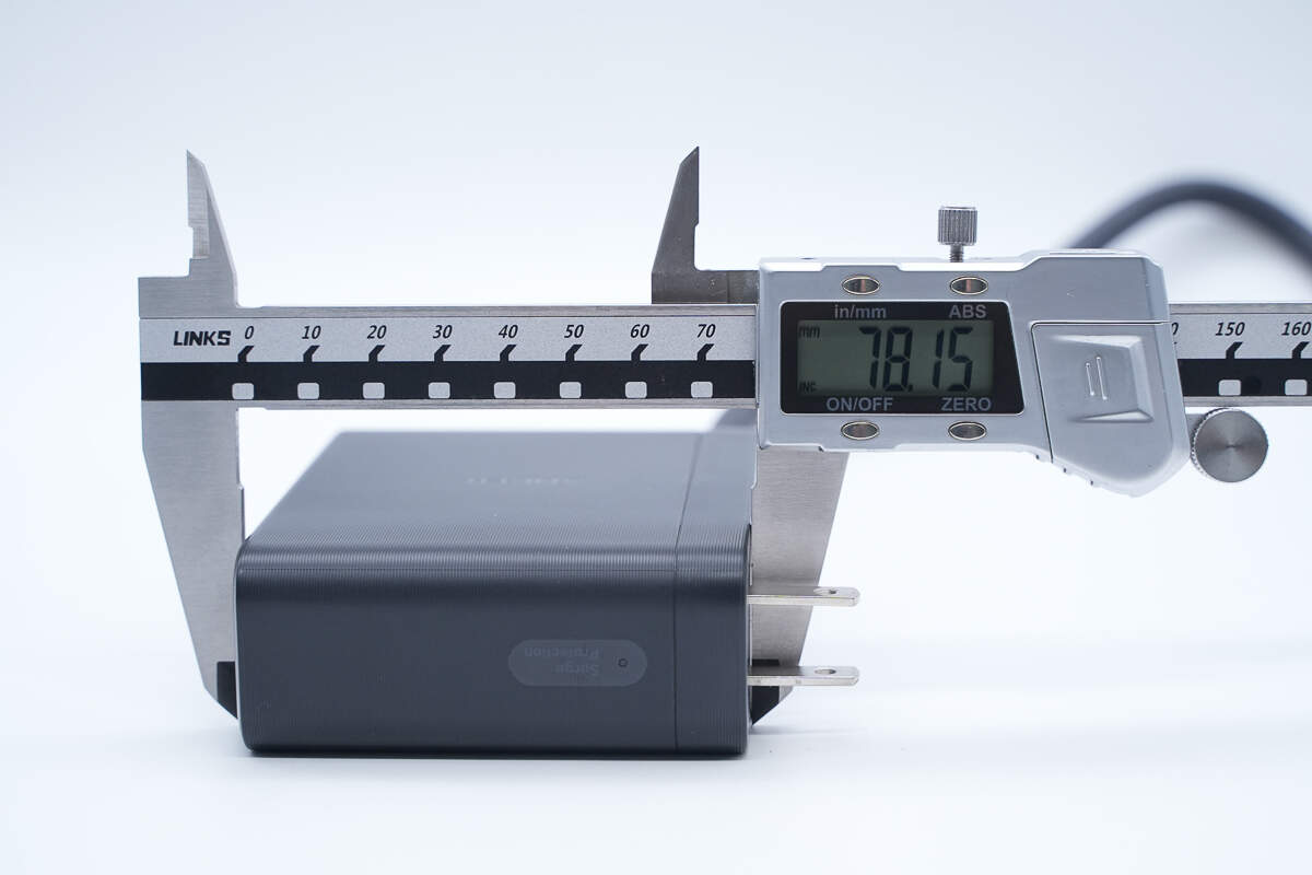
The height is about 78.15 mm (3.077 inches).
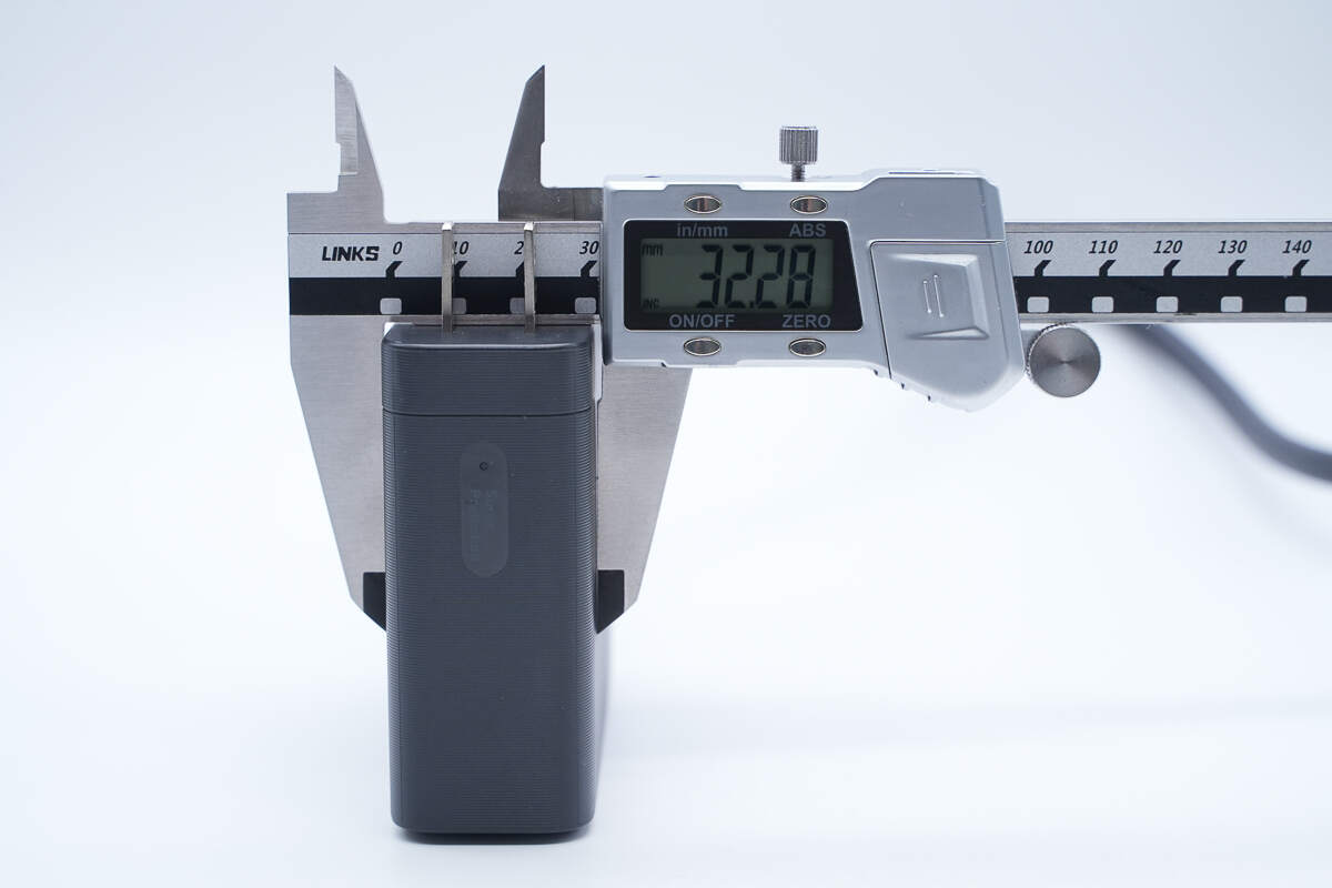
The width is about 32.28 mm (1.27 inches).
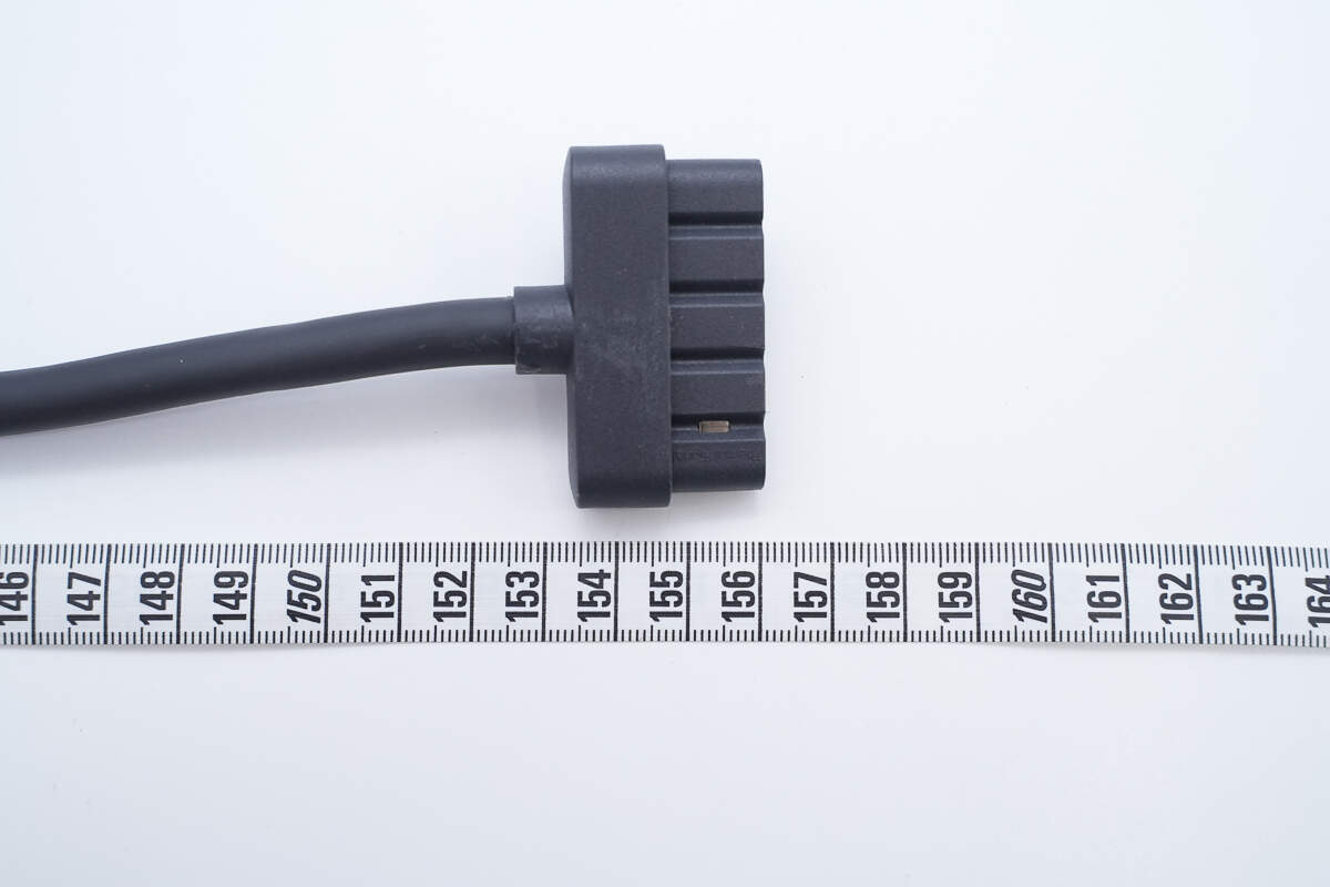
The length of the output cable is about 156 cm (5 feet 1.417 inches).
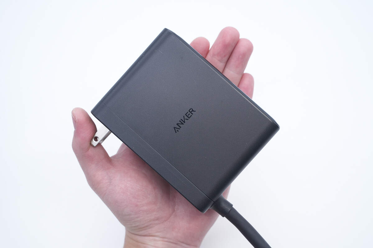
That's how big it is in the hand.
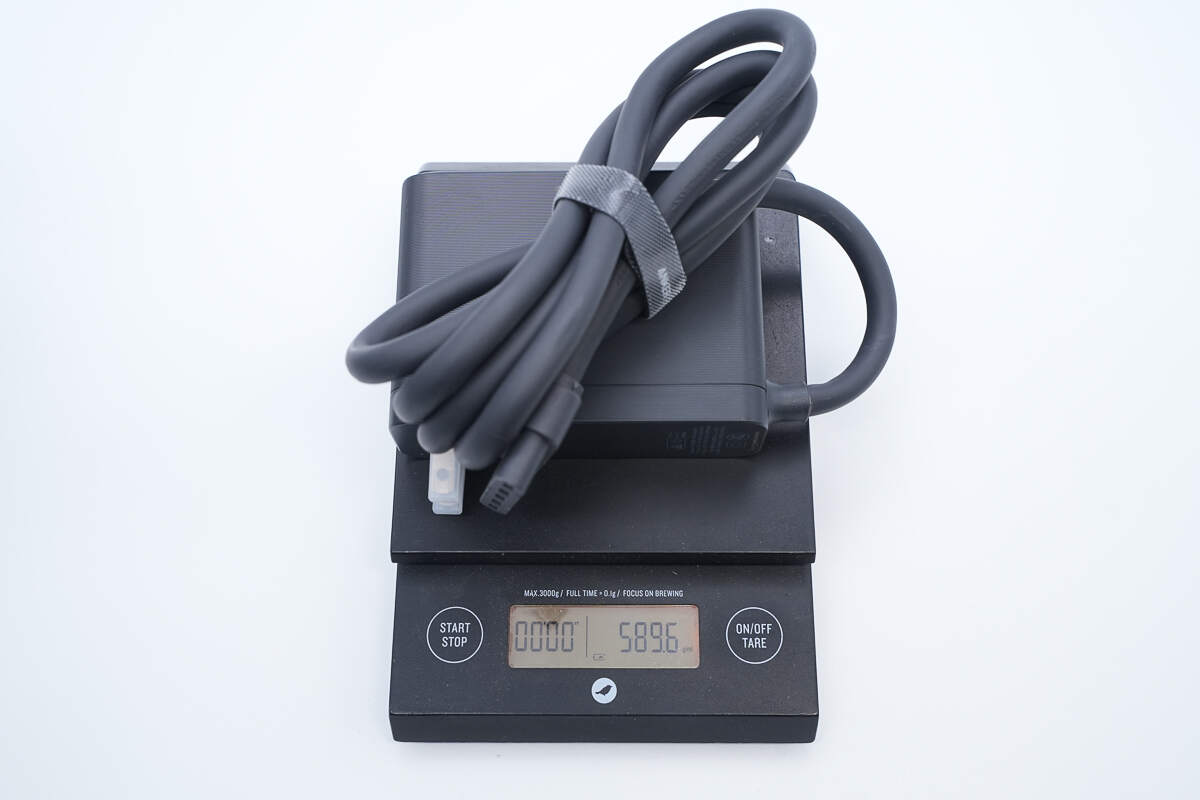
The weight is about 589.6 g (20.8 oz).
Teardown
Next, let's take it apart to see its internal components and structure.
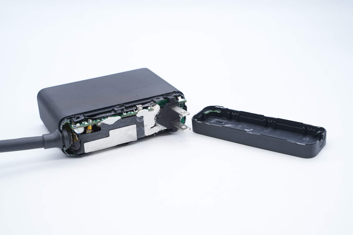
First, pry along the gap to open the input end cover.
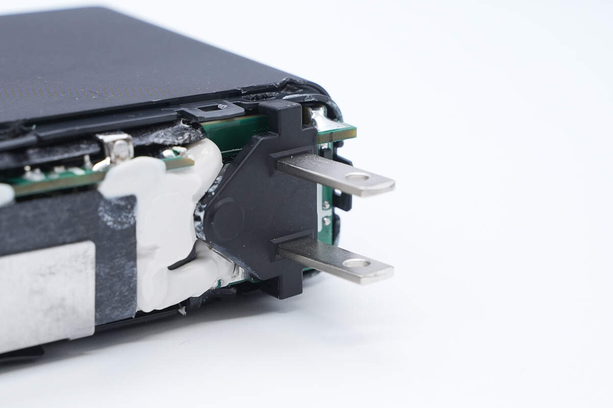
The input pins are reinforced and protected by a plastic frame.

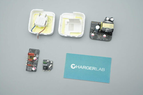
Take out the PCBA module, and there is a light guide on the inside of the case.
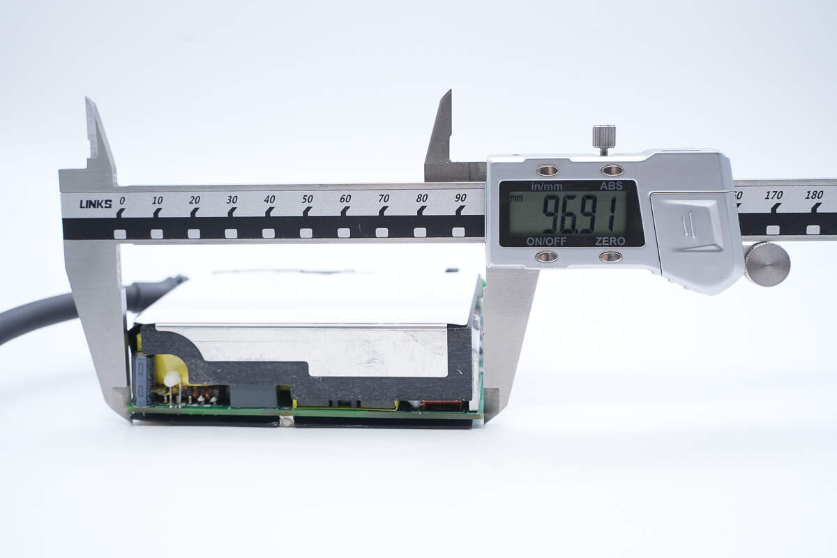
The length of the PCBA module is about 96.91 mm (3.82 inches).

The width is about 71.95 mm (2.83 inches).
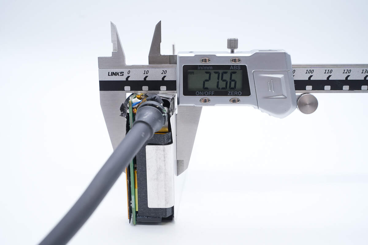
The thickness is about 27.56 mm (1.085 inches).
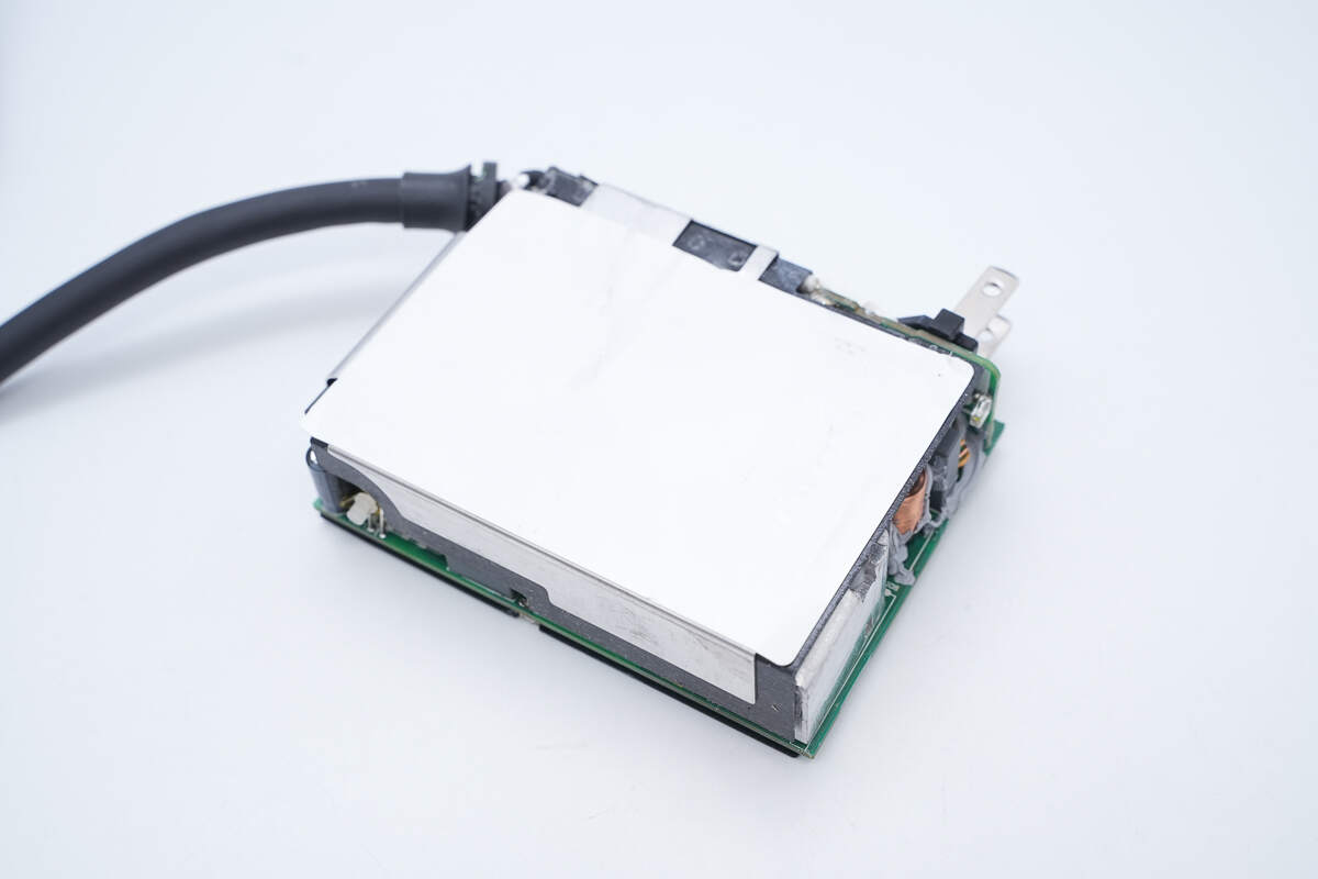
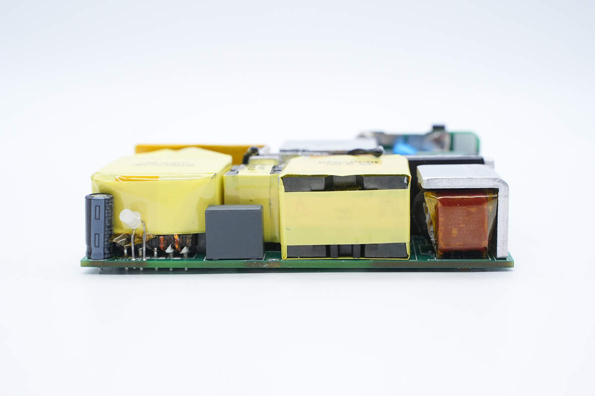
The PCBA module is covered with a heat sink, and the heat sink and the PCBA module are insulated with Mylar sheets.
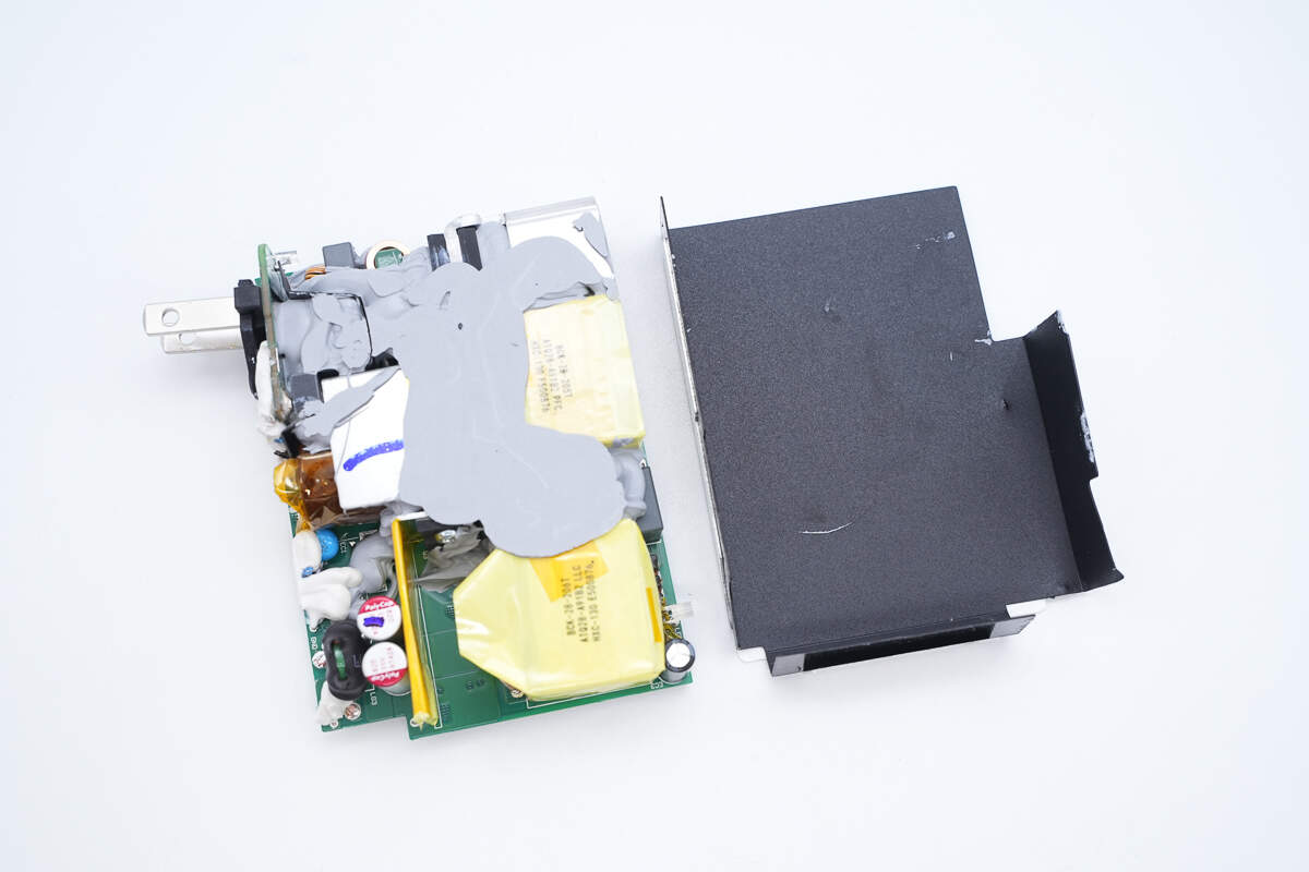
Remove the heat sink. The components on the front of the PCBA module are filled with potting compounds to help dissipate heat.
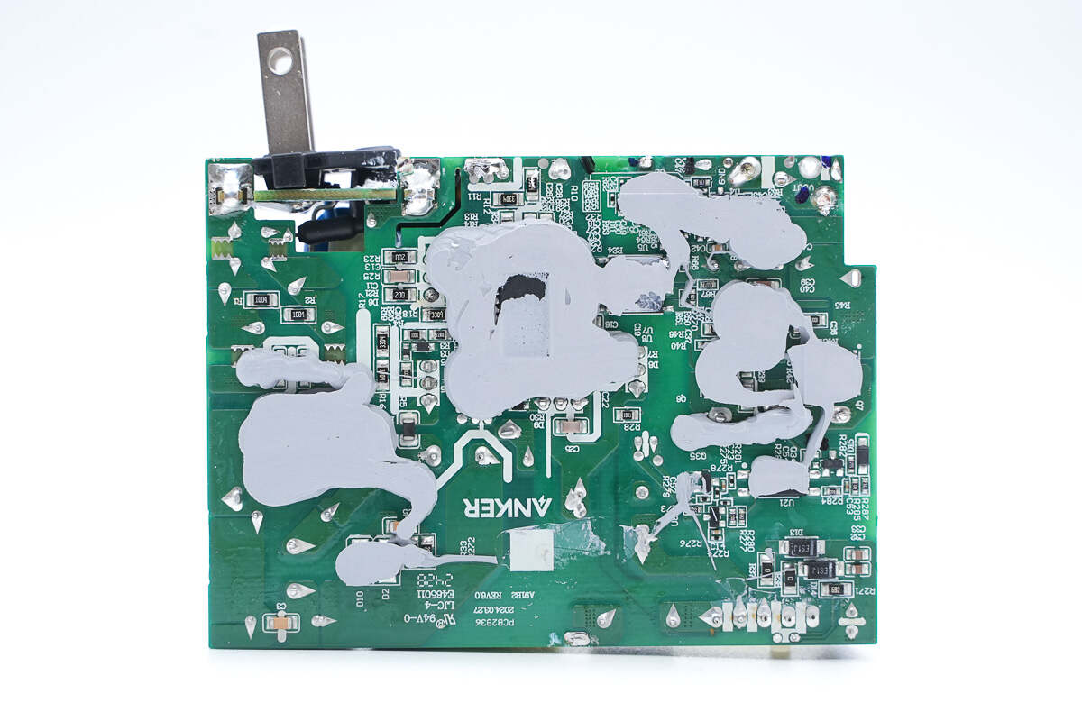
The components on the back are also filled with potting compounds to help dissipate heat.
Clean off the potting compound. The front of the PCBA module includes components such as a bridge rectifier, PFC MOSFET, primary MOSFET, and synchronous rectifier. All of them are equipped with heat sinks to help dissipate heat and thermistors for temperature detection.
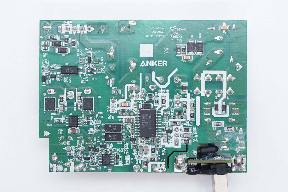
On the back are components such as a master control chip, synchronous rectifier controller, synchronous rectifier, optocoupler, etc.
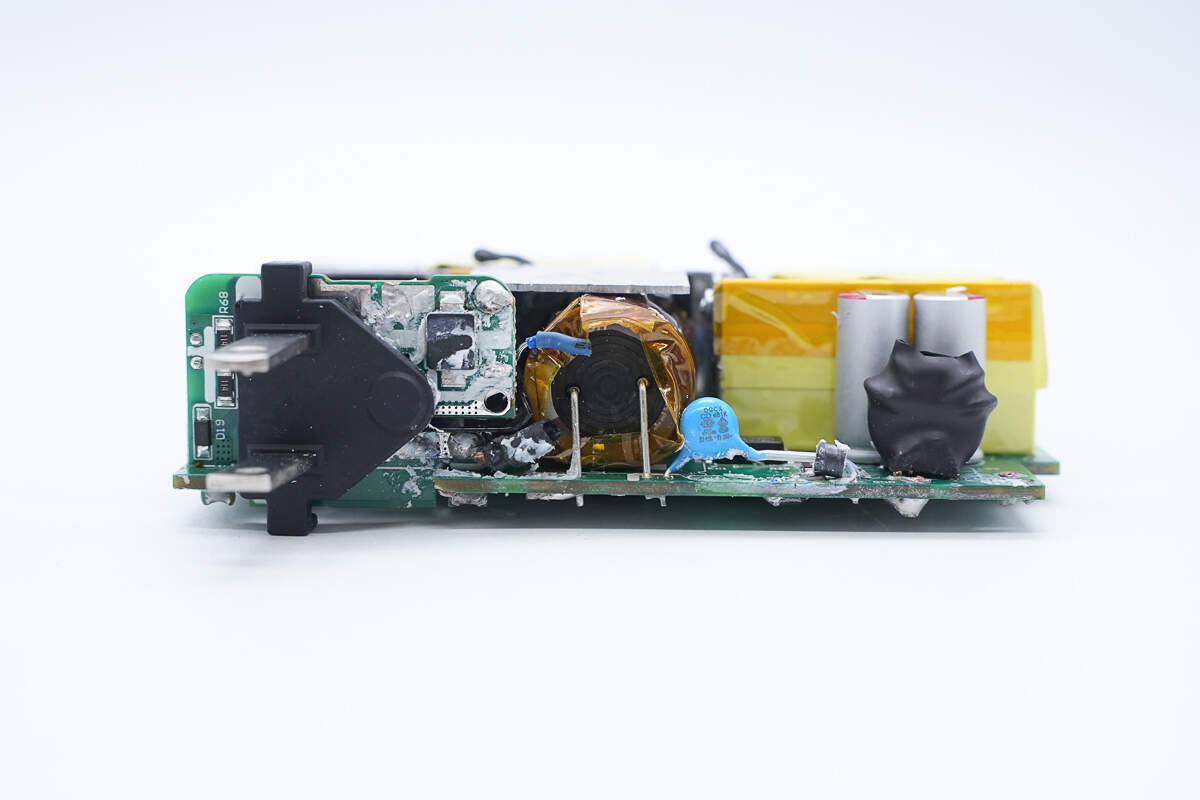
The input pins are soldered on a separate PCB. There is an SMD Y capacitor in the middle of this side. On the right is the electrolytic capacitor for input filtering, wrapped with heat-resistant tape for protection.
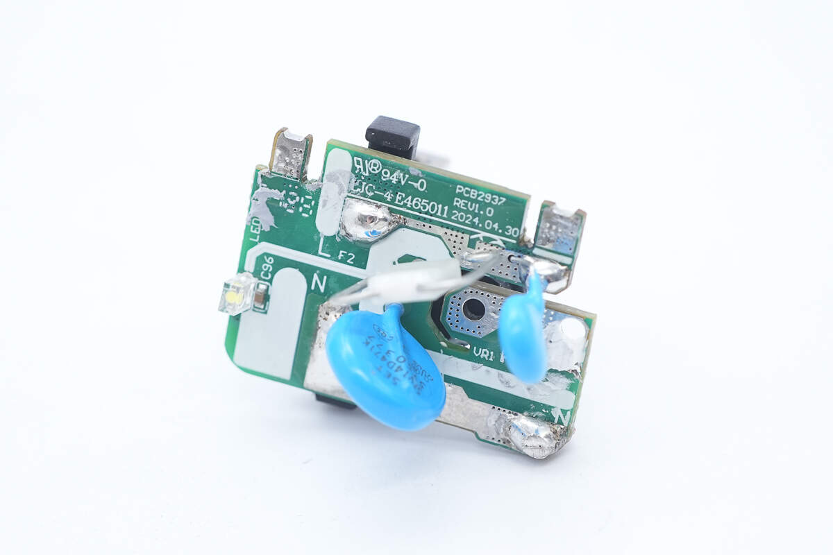
Take off the PCB of the pins, there is a varistor, thermal fuse, Y capacitor, and indicator light on the back.
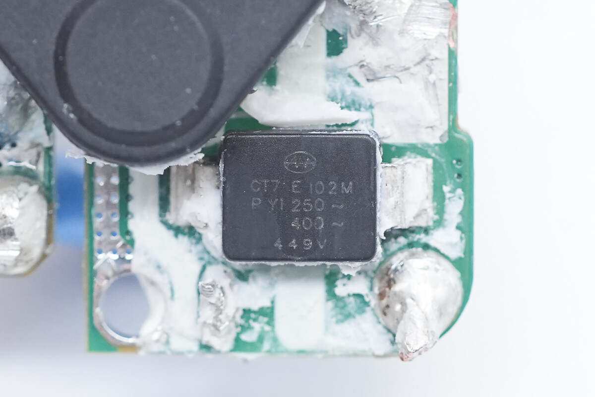
The SMD Y capacitor is from KeiFat.

The blue Y capacitor is from DGCX.
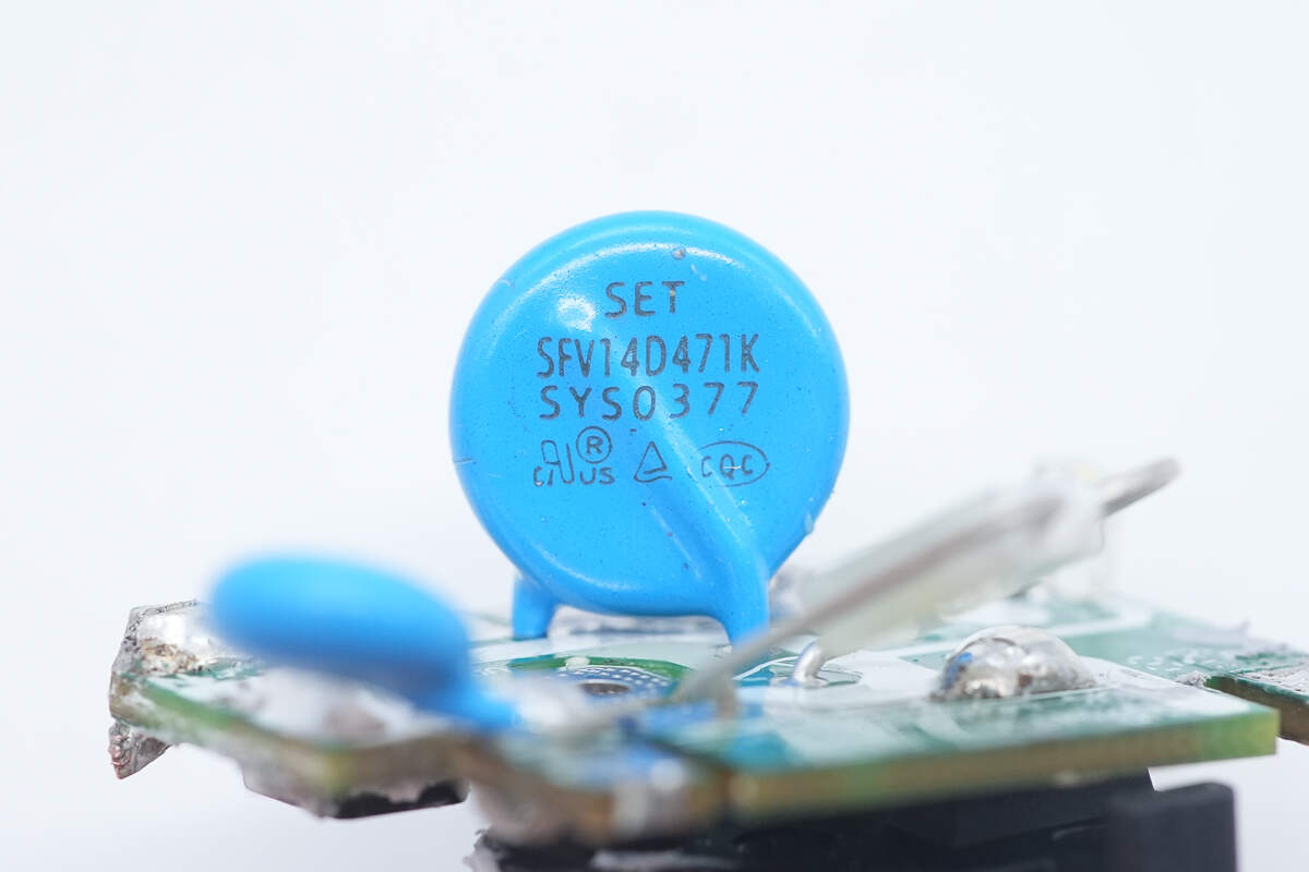
The varistor is from SET. It is an SFV14D series and is used for surge overvoltage protection. 470V. Model is SFV14D471K.
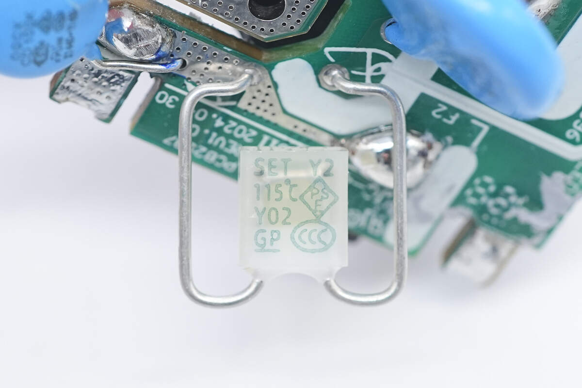
The thermal fuse is also from SET. It is a Y2 series 115℃ thermal fuse, used to detect the temperature rise of the varistor and provide overheat protection.

Here is the indicator light.
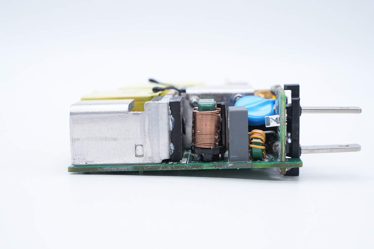
This side of the PCBA module has common mode inductors, safety X2 capacitor, and bridge rectifier.
Remove the bridge rectifiers and heat sink. The two bridge rectifiers are fixed on both sides of the heat sink by screws.
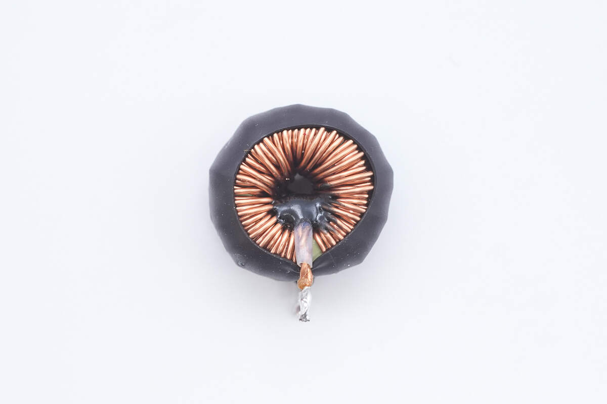
The common mode inductor is used to filter out EMI interference. This one is wound with two wires.
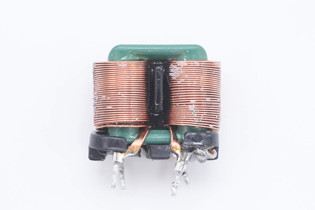
The other is wound with flat copper tape.
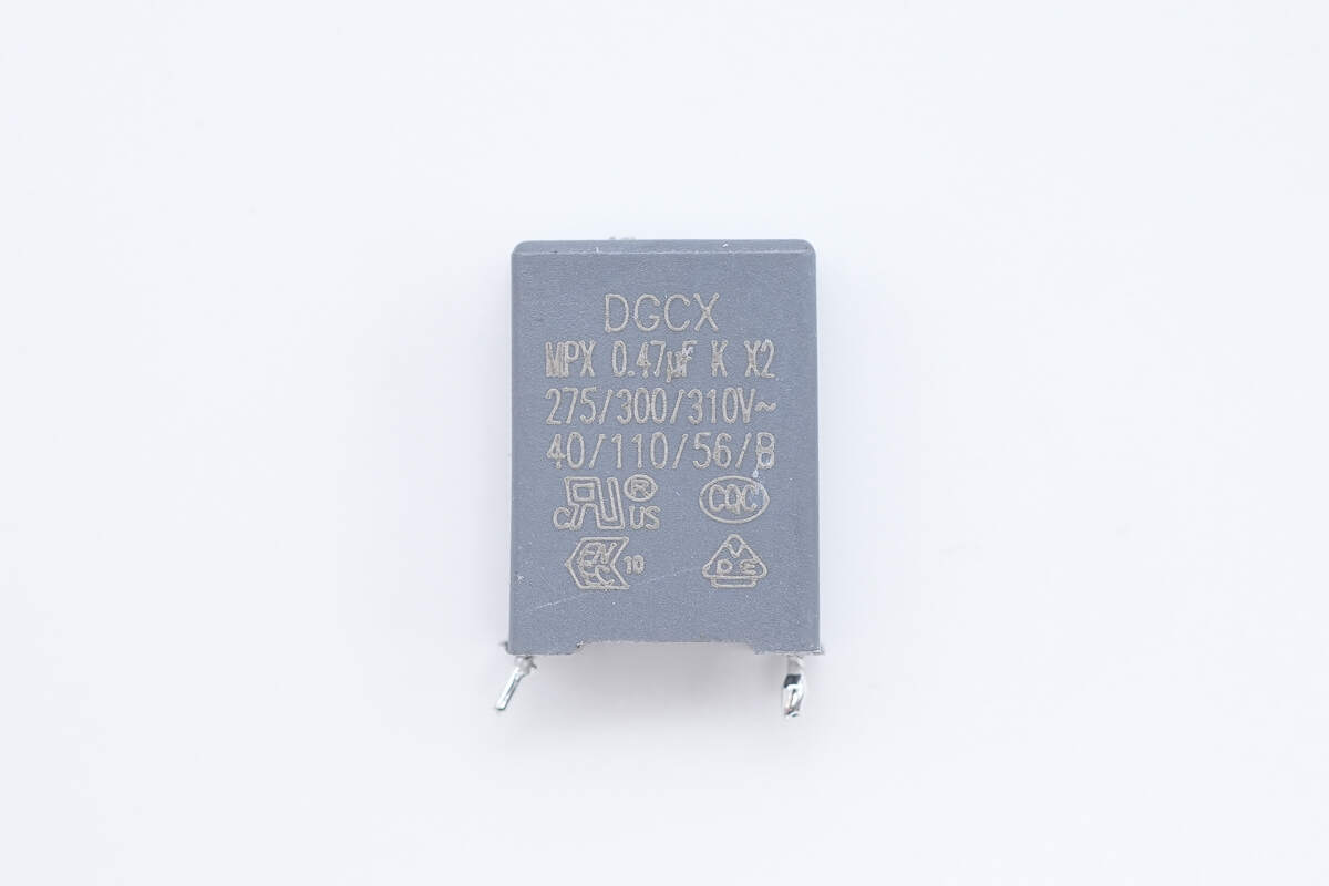
The safety X2 capacitor is from DGCX. 0.47μF.
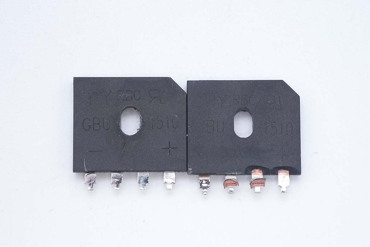
The two bridge rectifiers are from Pingwei and adopt GBU package. 15A 1000V. Model is GBU1510.
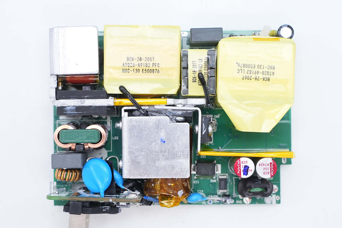
This end of the module is equipped with film capacitor, PFC boost inductor, resonant inductor, and resonant capacitor.
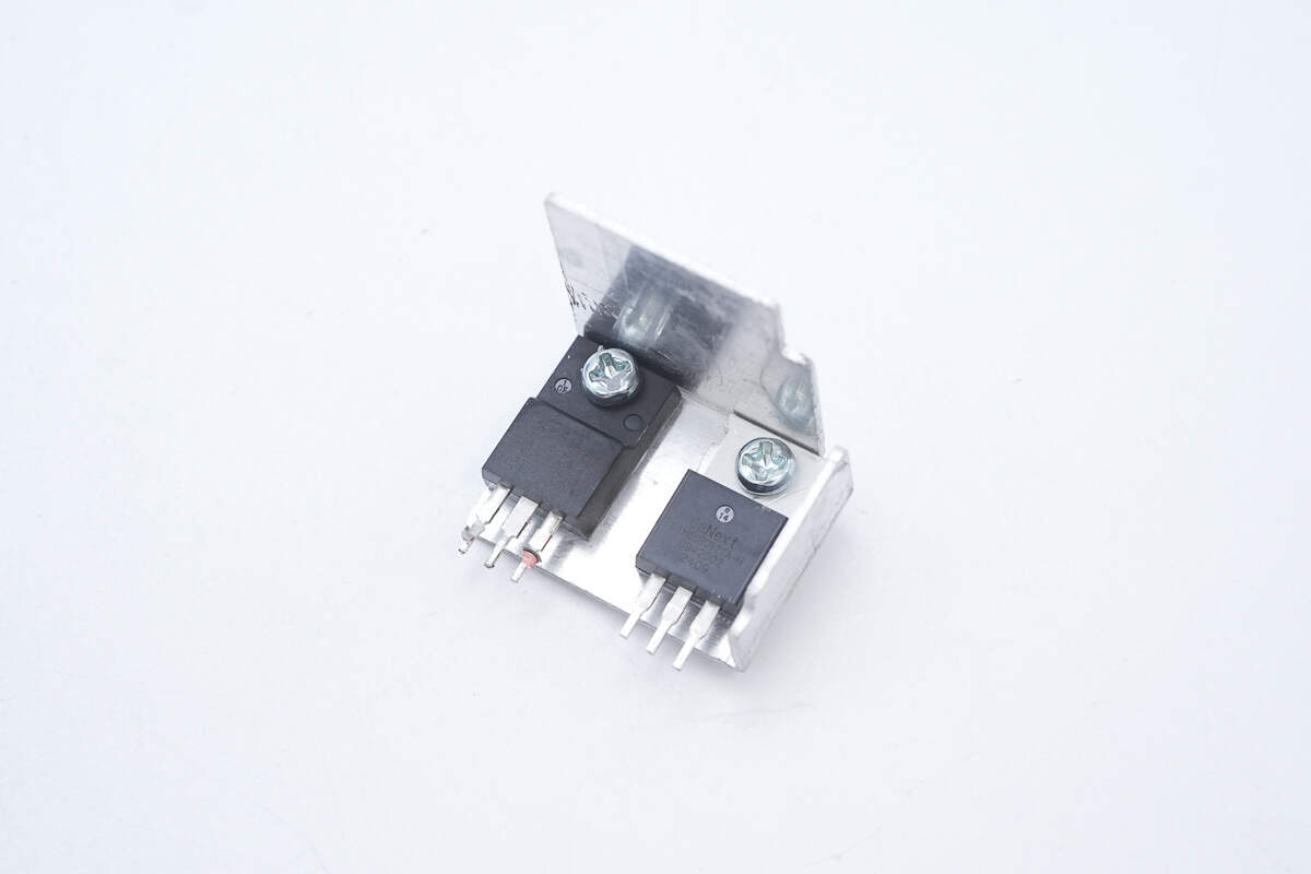
Remove another heat sink, with the PFC MOSFET and PFC rectifier fixed on it.
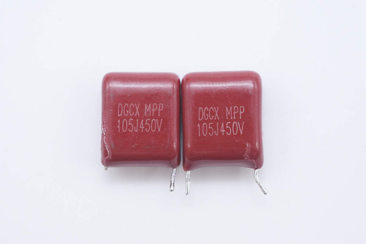
These two MPP film capacitors are also from DGCX. 1μF 450V.
The filter inductor is insulated by heat-shrinkable tubing.
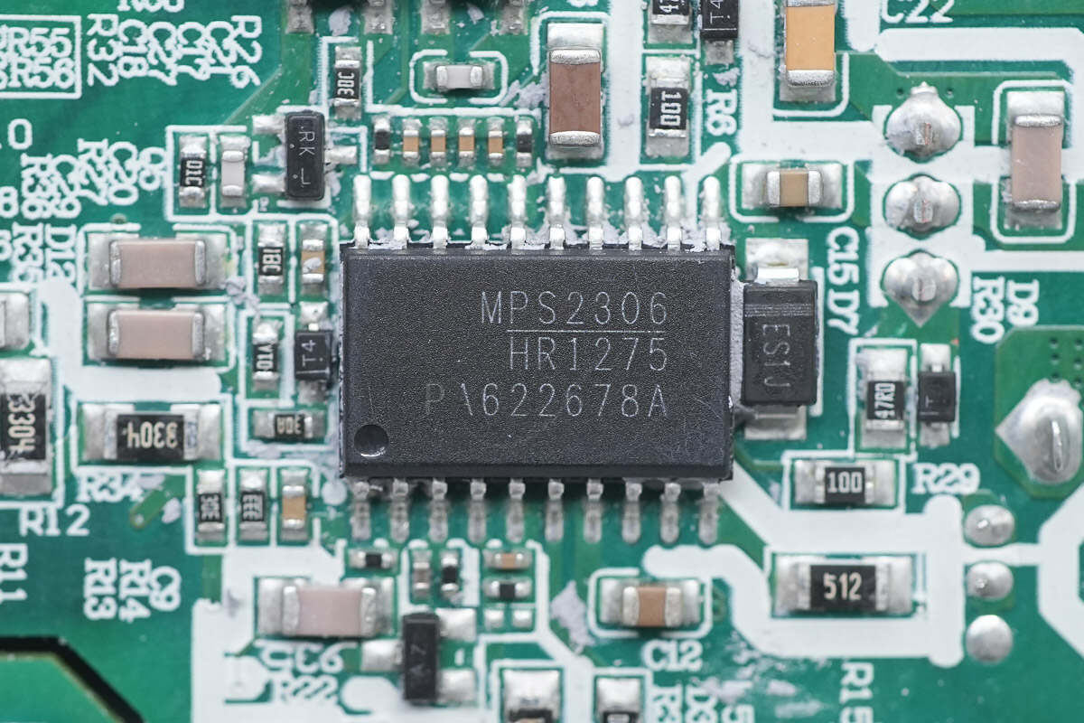
The master control chip is from MPS. It adopts critical and discontinuous mixed-mode PFC control with the current mode, which can be configured through the UART interface. It has built-in power-saving technology to help achieve efficiency optimization in the whole working range. It has built-in high voltage startup and X capacitor discharge and supports PG signal output. Model is HR1275.
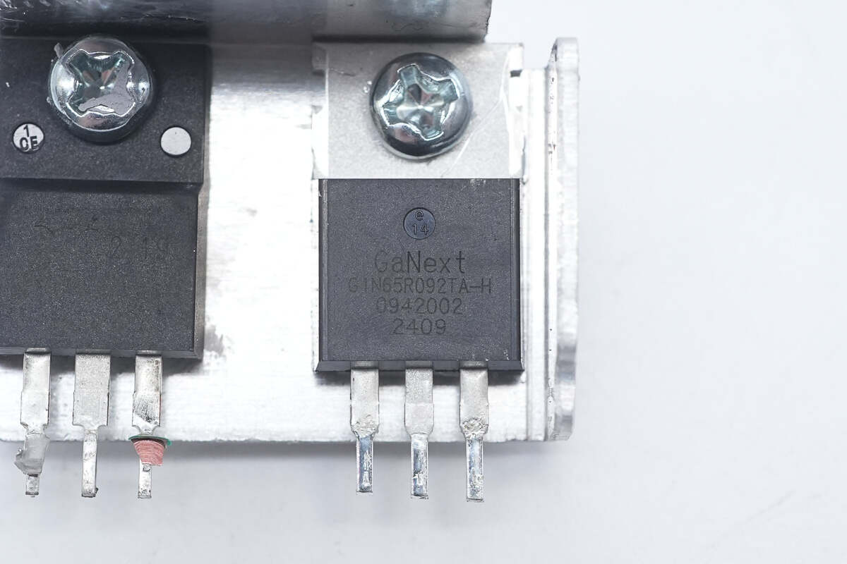
The PFC boost MOSFET is from GaNext and adopts TO-220 package. It has a withstand voltage of 650V and a resistance of 92mΩ. Model is G1N65R092TA-H.
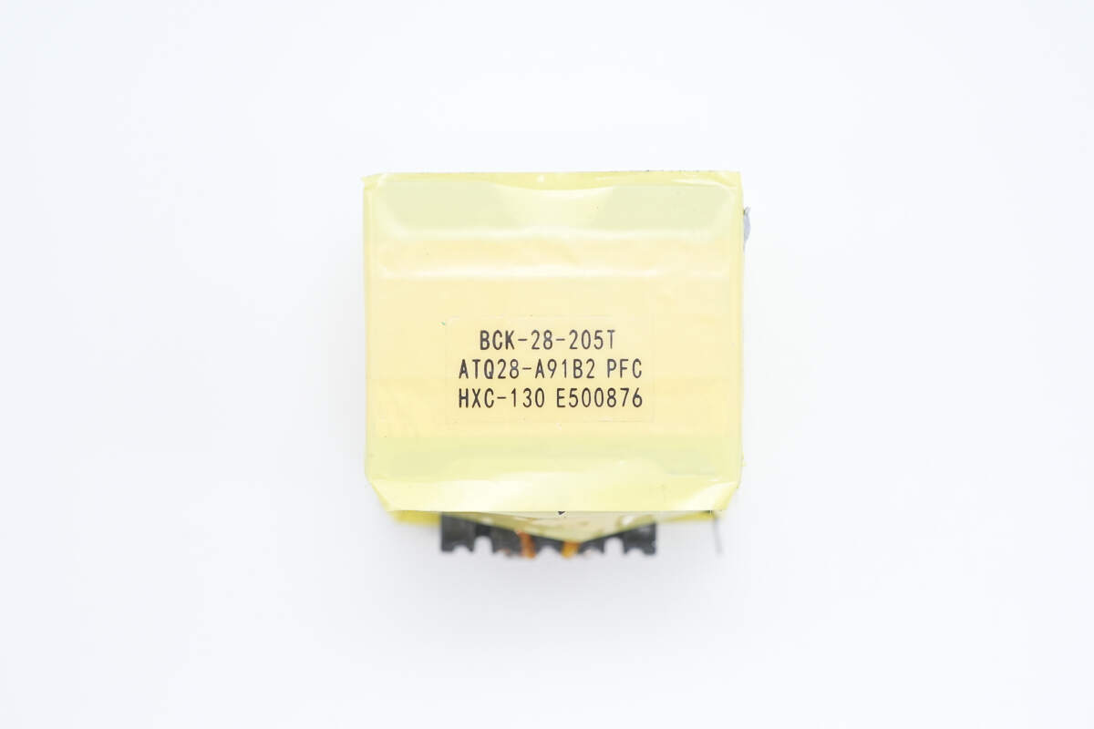
The PFC boost inductor adopts the ATQ28 core.
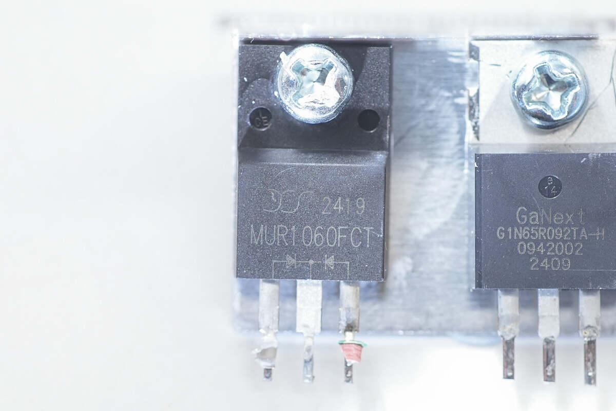
The PFC rectifier is from YJ and adopts ITO-220AB package. 600V 10A. Model is MUR1060FCT.
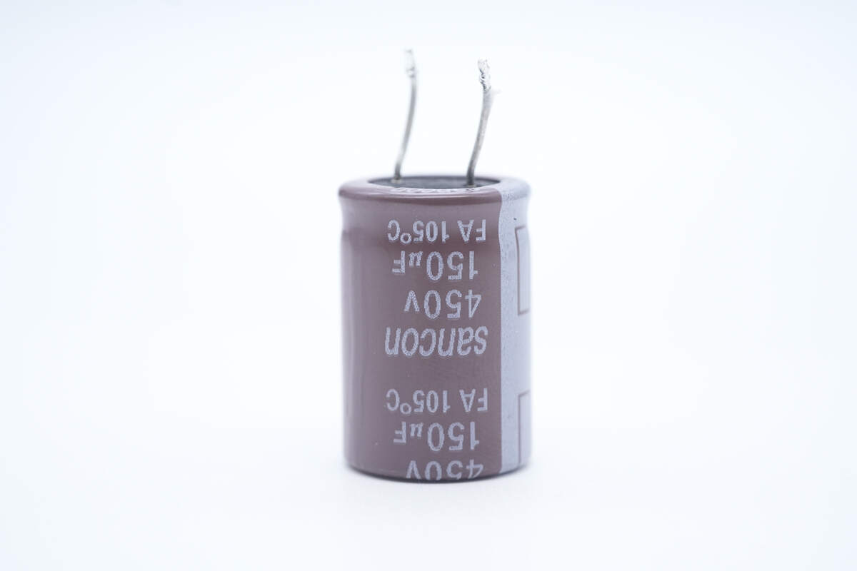
The electrolytic capacitor for input filtering is from Sancon. 450V 150μF.
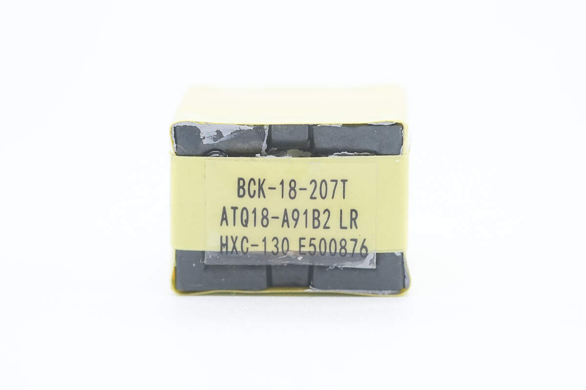
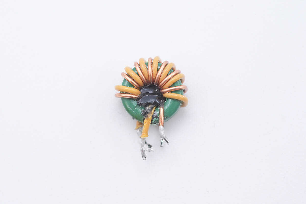
Here is the resonant inductor.
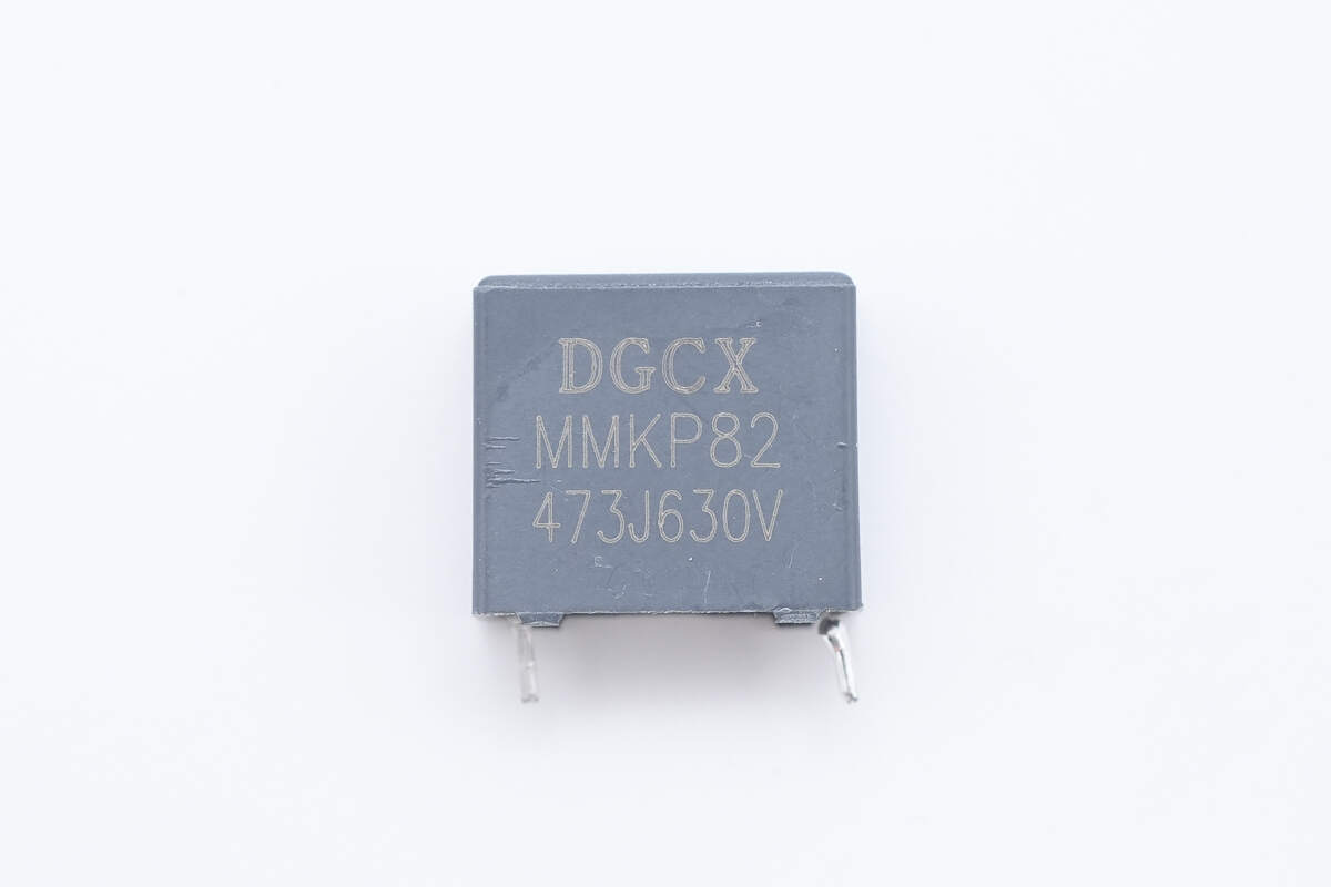
The resonant capacitor is from DGCX. 0.047μF 630V.
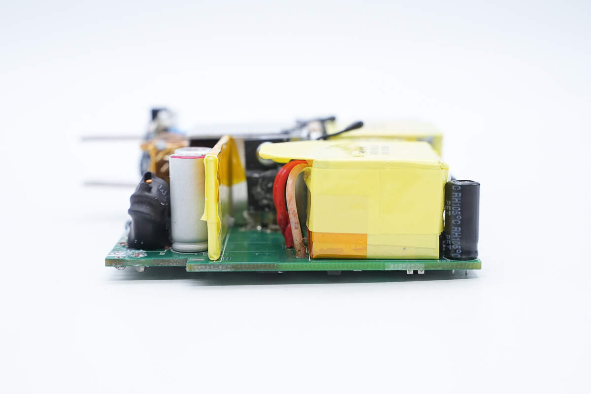
This side of the module is equipped with planar transformer, power supply capacitor for the master control chip, solid capacitor for output filtering, filter inductor, and other components.
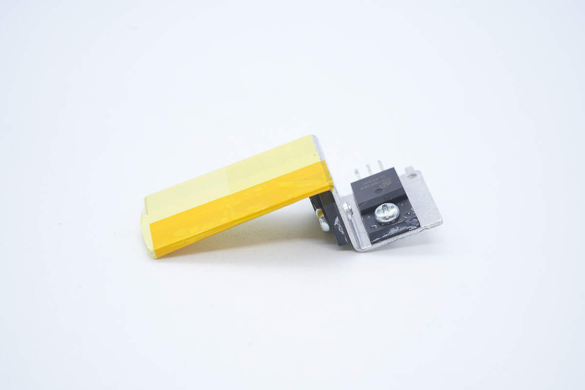
Remove the third heat sink, with two LLC half-bridge MOSFETs fixed on it.
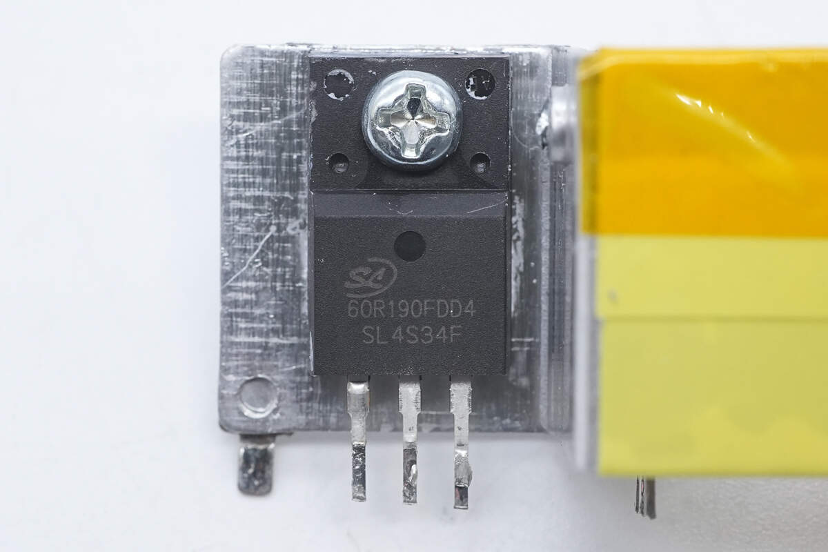
The LLC half-bridge MOSFET is from Silan and adopts TO-220FJD-3L package. It has a withstand voltage of 600V and a resistance of 0.165Ω. Model is SVS60R190FJDD4.
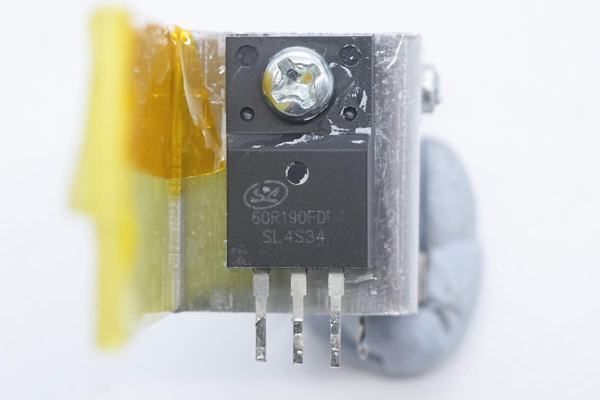
The second LLC half-bridge MOSFET is identical to the first one.
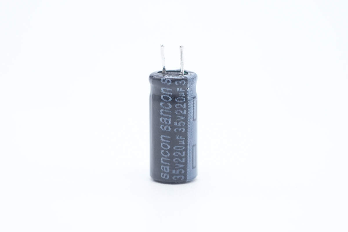
The power supply capacitor for the master control chip is also from Sancon. 35V 220μF.
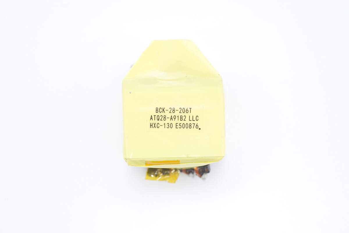
Here is the planar transformer.

The blue Y capacitor is from DGCX.
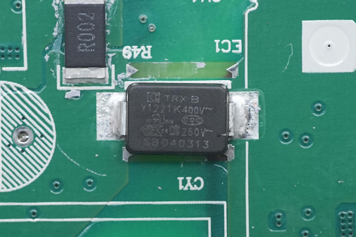
The SMD Y capacitor is from TRX. Its small size and light weight are suitable for high-density power products such as GaN fast chargers.
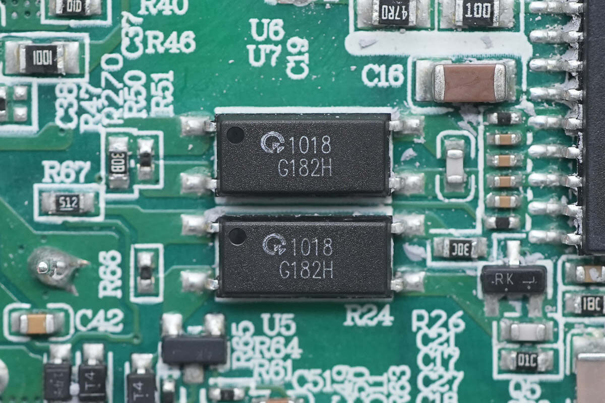
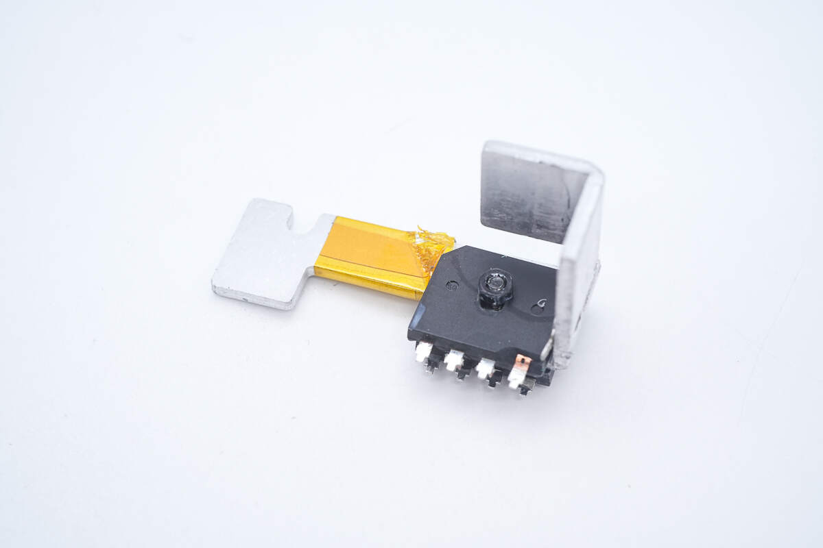
These two optocouplers marked with 1018 are used for output voltage feedback and protection functions.
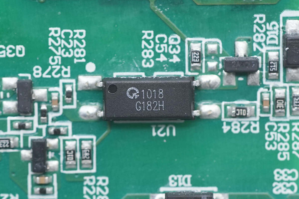
This is the third optocoupler.
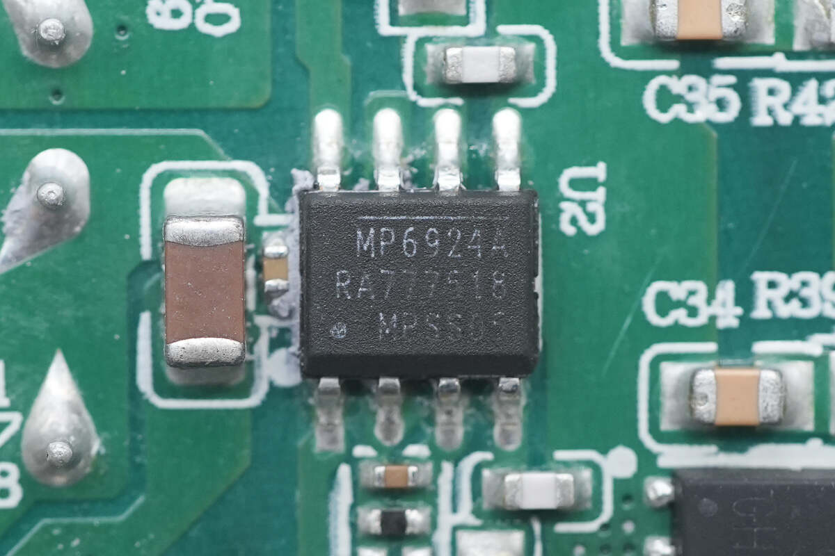
The synchronous rectifier controller is from MPS. It has stronger anti-interference and fast shutdown function and is compatible with CCM/DCM mode. It integrates two synchronous rectifier controllers, which are used for the rectification application of the two secondary coil outputs of LLC, and is suitable for LLC converter synchronous rectification application. Model is MP6924A.
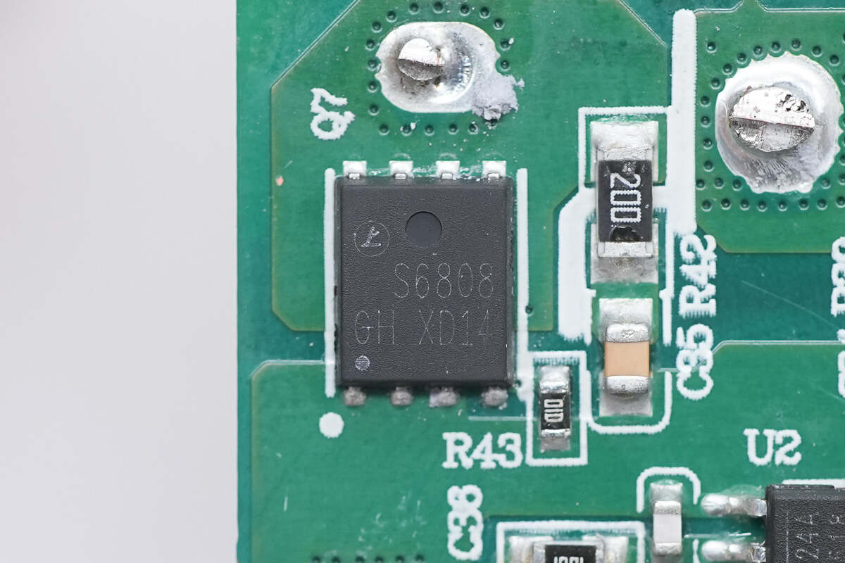
The synchronous rectifier is marked with S6808.
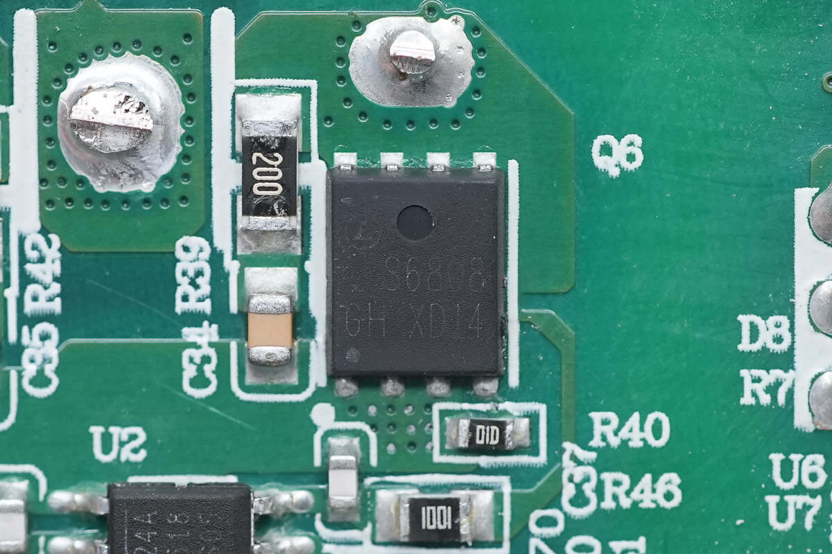
The other synchronous rectifier is also marked with S6808.

These two solid capacitors for output filtering are from Polycap. 35V 820μF.
The filter inductor is insulated by heat-shrinkable tubing.
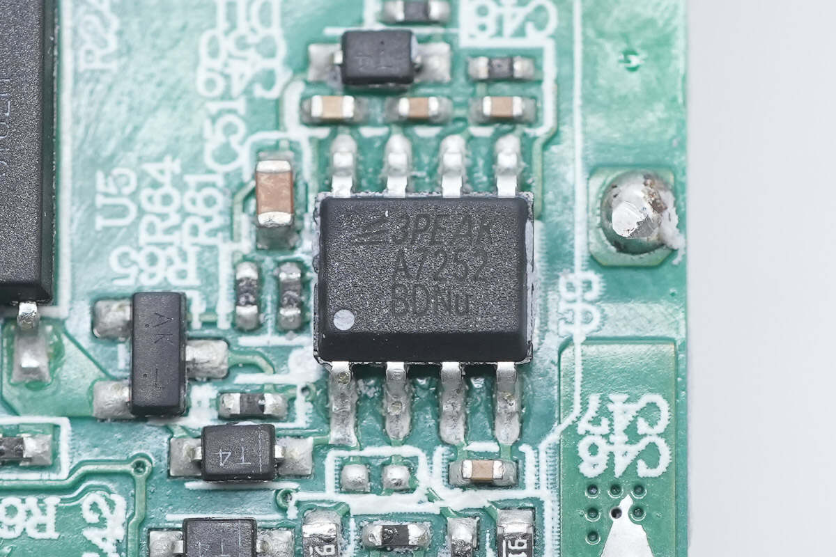
The Op-Amp is from 3PEAK. Model is TPA7252.
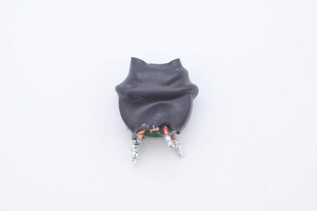
Here is the thermistor.

Here is the indicator light.
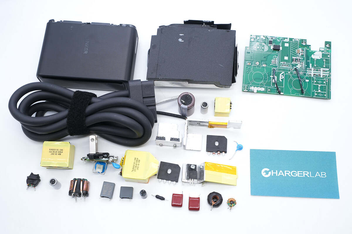
Well, those are all components of the ANKER 253W GaN Power Adapter.
Summary of ChargerLAB
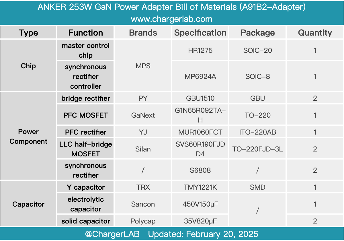
Here is the component list of the ANKER 253W GaN Power Adapter for your convenience.
The design of the Anker 253W GaN power adapter continues its style and is equipped with an indicator light for surge protection and a light ring to indicate whether it is powered on, enhancing the user experience. Because of its unique output connector, it can provide AC or DC power supply.
After taking it apart, we found it adopts a PFC+LLC+SR power supply architecture design. There are many heat sinks inside, the PCBA module is filled with potting compound and covered with a large heat sink to help dissipate heat. The workmanship and materials are solid and reliable.
Related Articles:
1. Teardown of ANKER 150W 4 Ports GaN Charger (A2655)
2. Teardown of ANKER Prime 250W GaN Charger (A2345)
3. Teardown of Anker Prime 200W 6 Ports GaN Charger