Introduction
Texas Instruments (TI) recently announced that its factory in Aizu, Japan, has fully commenced production of power semiconductors based on gallium nitride (GaN) technology. By continuously expanding its in-house manufacturing capabilities, TI has achieved a fourfold increase in GaN production capacity, providing the global market with more high-performance power solutions.
Industry-Leading GaN Manufacturing Capabilities
Currently, TI’s two global wafer fabs—located in Dallas, USA, and Aizu, Japan—are fully operational in GaN chip mass production, with end-to-end control of critical processes and core technologies. This vertically integrated model allows TI to efficiently scale production capacity while ensuring significant optimization in product quality and manufacturing costs.
Mohammad Yunus, Senior Vice President of TI’s Technology and Manufacturing Group, stated: "Building on decades of expertise in GaN chip design and manufacturing, TI has successfully validated its 8-inch GaN technology and is now moving into mass production. This scalable and cost-effective GaN manufacturing approach marks a significant milestone. By 2030, we expect more than 95% of our manufacturing capacity to be in-house, with multiple fab sources to ensure a stable supply of TI’s entire lineup of high-power, high-efficiency GaN semiconductor products."
Furthermore, TI has successfully validated its GaN manufacturing process based on 12-inch (300mm) wafers and launched a pilot project. Compared to 8-inch wafers, 12-inch wafers can produce 2.3 times more chips per wafer, significantly advancing both technology and efficiency. This marks an important step in TI's innovation and manufacturing efficiency, paving the way for a full transition to 12-inch wafer technology in the future.
Unique Advantages of GaN Technology
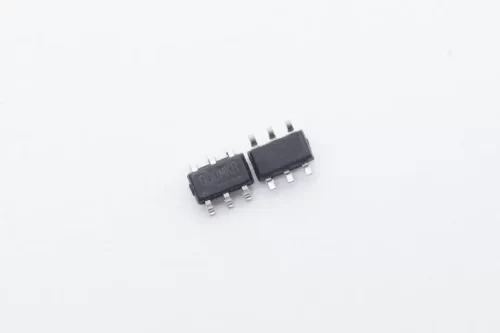
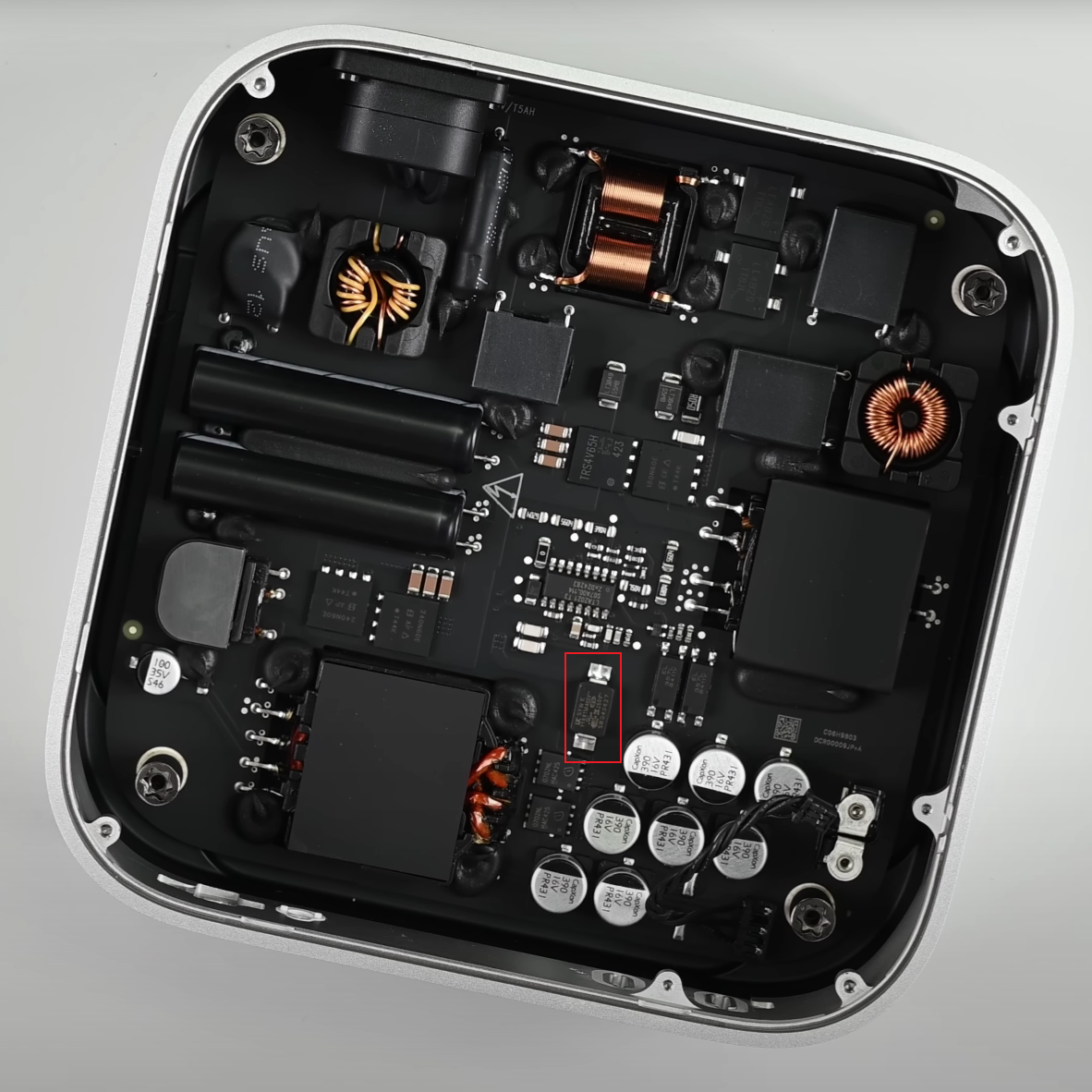
As an ideal alternative to silicon-based materials, GaN technology offers significant performance advantages across multiple dimensions. With superior energy efficiency and ultra-high switching speeds, GaN materials enable more compact and lightweight system designs while maintaining exceptional stability and reliability under high-temperature and high-voltage conditions. TI’s GaN solutions feature highly integrated designs, simplifying customer development processes, improving end-product reliability and performance, and reducing overall system costs.
TI plans to expand GaN technology applications to higher voltage ranges, starting at 900V and gradually moving to even higher voltages to support diverse high-efficiency application scenarios. These applications include robotics, renewable energy systems, and next-generation server power supplies. Moreover, TI’s GaN technology is based on its proprietary GaN-on-Silicon process, which has undergone over 80 million hours of reliability testing and integrates multiple protection mechanisms to provide enhanced safety for high-voltage systems.
Kannan Soundarapandian, Vice President of TI’s High Voltage Power Division, remarked:
"GaN technology allows us to deliver higher power in more compact systems, meeting our customers' core demands for power optimization and efficiency improvements."
Sustainable Manufacturing and Environmental Benefits
TI has adopted cutting-edge GaN chip manufacturing equipment to enhance product performance, process efficiency, and cost advantages. Additionally, TI's advanced and efficient machines for increased GaN capacity enable the production of smaller yet more powerful chips. This design innovation uses fewer water resources, energy, and raw materials in manufacturing, while end-products adopting GaN chips also inherit similar environmental benefits.
Summary of ChargerLAB
With continued investments and innovations in technology, TI is driving the widespread adoption of GaN technology globally, achieving significant breakthroughs in manufacturing capacity, product performance, and cost efficiency. Through advanced manufacturing processes and eco-friendly design principles, TI has not only achieved technological milestones but also set a benchmark in sustainable development, demonstrating its steadfast commitment to social responsibility.
At the same time, TI has made substantial progress in developing 12-inch GaN power wafers. This strategic move will further propel the rapid development of high-efficiency, high-power-density electronic products, injecting more vitality and innovation into the industry. Looking ahead, we anticipate TI continuing to lead the transformation of GaN technology, pioneering even more groundbreaking industry advancements.