Introduction
Previously, ChargerLAB conducted a teardown of a tp-link USB-C 3-in-1 docking station, a compact solution featuring 100W PD pass-through charging, 4K@60Hz video output, and a high-speed USB 3.0 port. Building on this, We’ve just received tp-link’s latest 9-in-1 docking station, and we’re ready to dive into what makes this expanded hub the next big thing in desktop connectivity.
It is a connectivity powerhouse, which includes 4K@60Hz HDMI, 100W PD charging, USB-A ports, Gigabit Ethernet, and dual SD/TF card slots—making it the perfect hub for your peripherals, camera gear, and external monitors.
It’s housed in a rugged, space-gray aluminum body that features a clever self-storing cable design: the USB-C plug clicks directly into the rear of the unit to serve as a carry loop. It’s a smart fix for that old headache of snagging or scratching your other gadgets while on the move.
Now, ChargerLAB takes you under the hood for a deep-dive teardown of the tp-link 9-in-1 dock.
Product Appearance

The box comes in tp-link’s iconic lake-blue, with a clear product shot front and center. You’ll also find all the critical specs highlighted right on the front, including the 9-in-1 capability, 4K@60Hz output, 100W PD power delivery, and the built-in Gigabit Ethernet port.
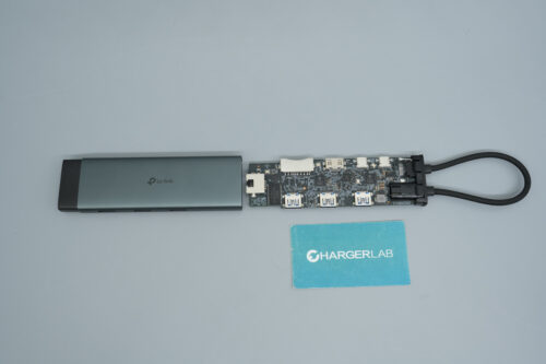
The side panel of the box shows that it supports macOS, Windows, Linux, iPadOS, iOS, Android, and ChromeOS.

The back of the box features a visual guide for connection scenarios and a complete list of technical specs for all available ports.
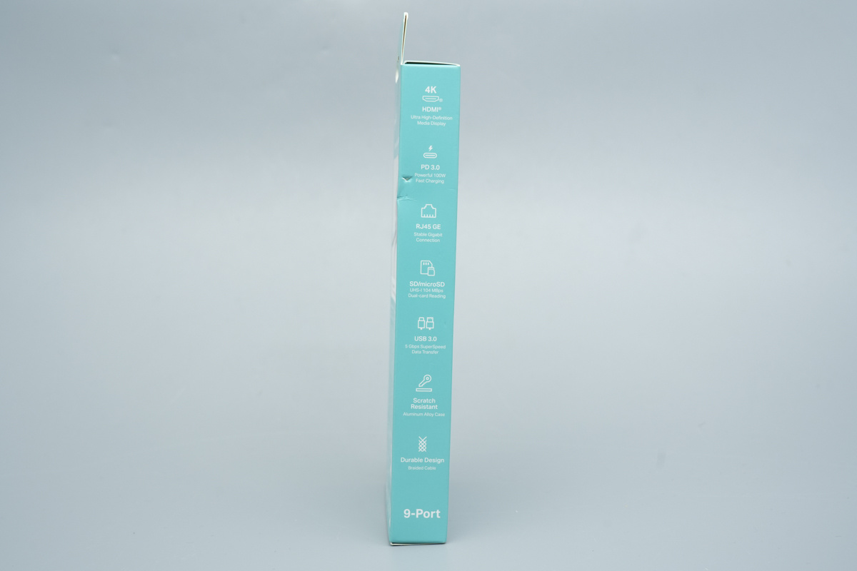
The product’s key selling points printed right on the side.
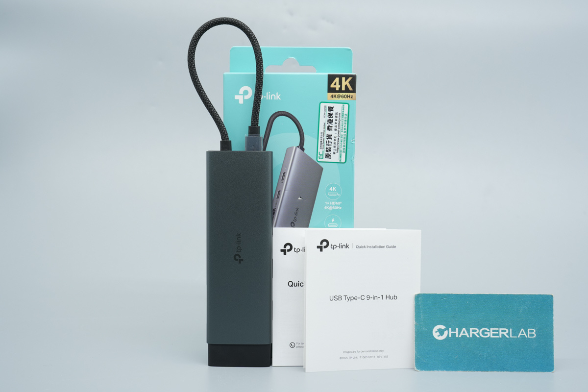
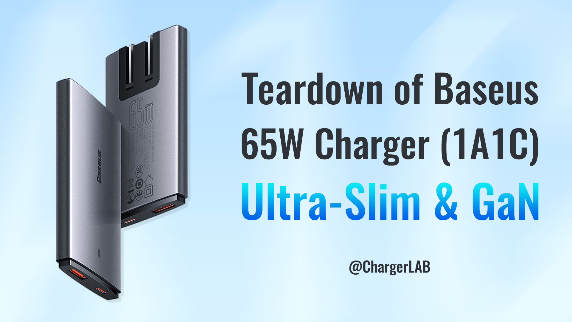
Opening the box reveals the docking station itself, and a quick-start guide.
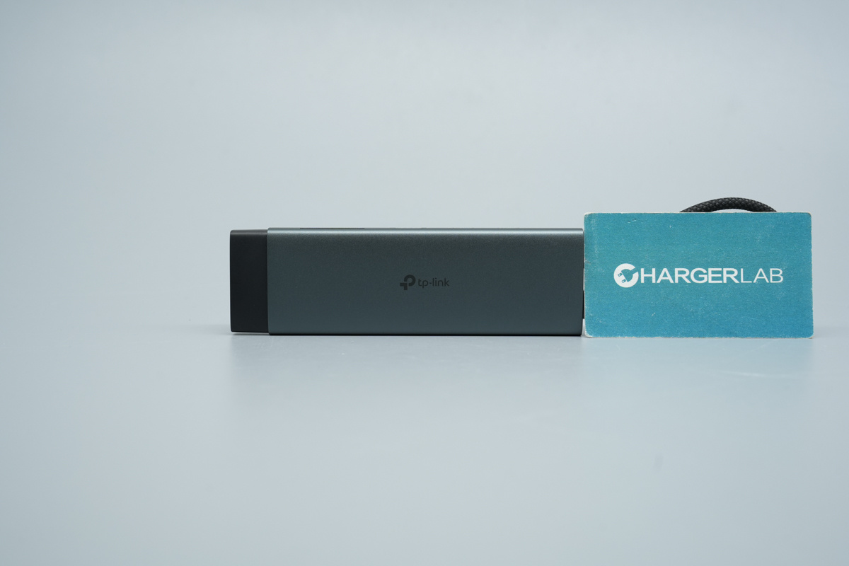
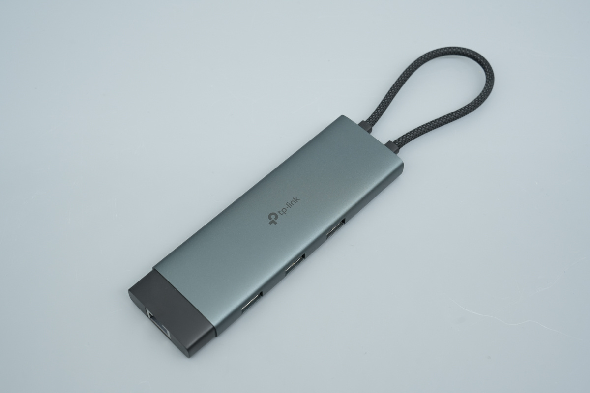
The dock features a durable space-gray anodized aluminum housing with a self-storing braided cable that docks into the rear to create a convenient carry handle.
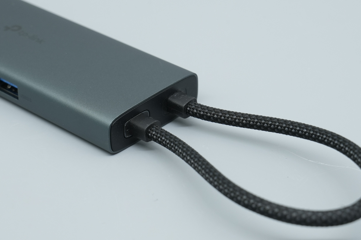
The rear of the dock is cleverly designed with a dedicated slot for the USB-C connector, letting it snap neatly into the body for easy, secure transport.
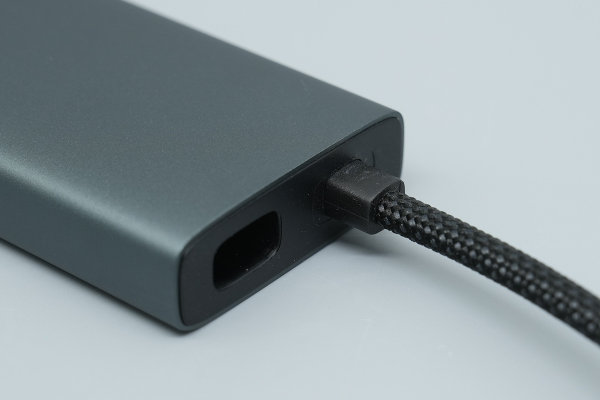
With the USB-C connector removed, the internal stowage channel is clearly revealed, demonstrating a dedicated design for secure integration.
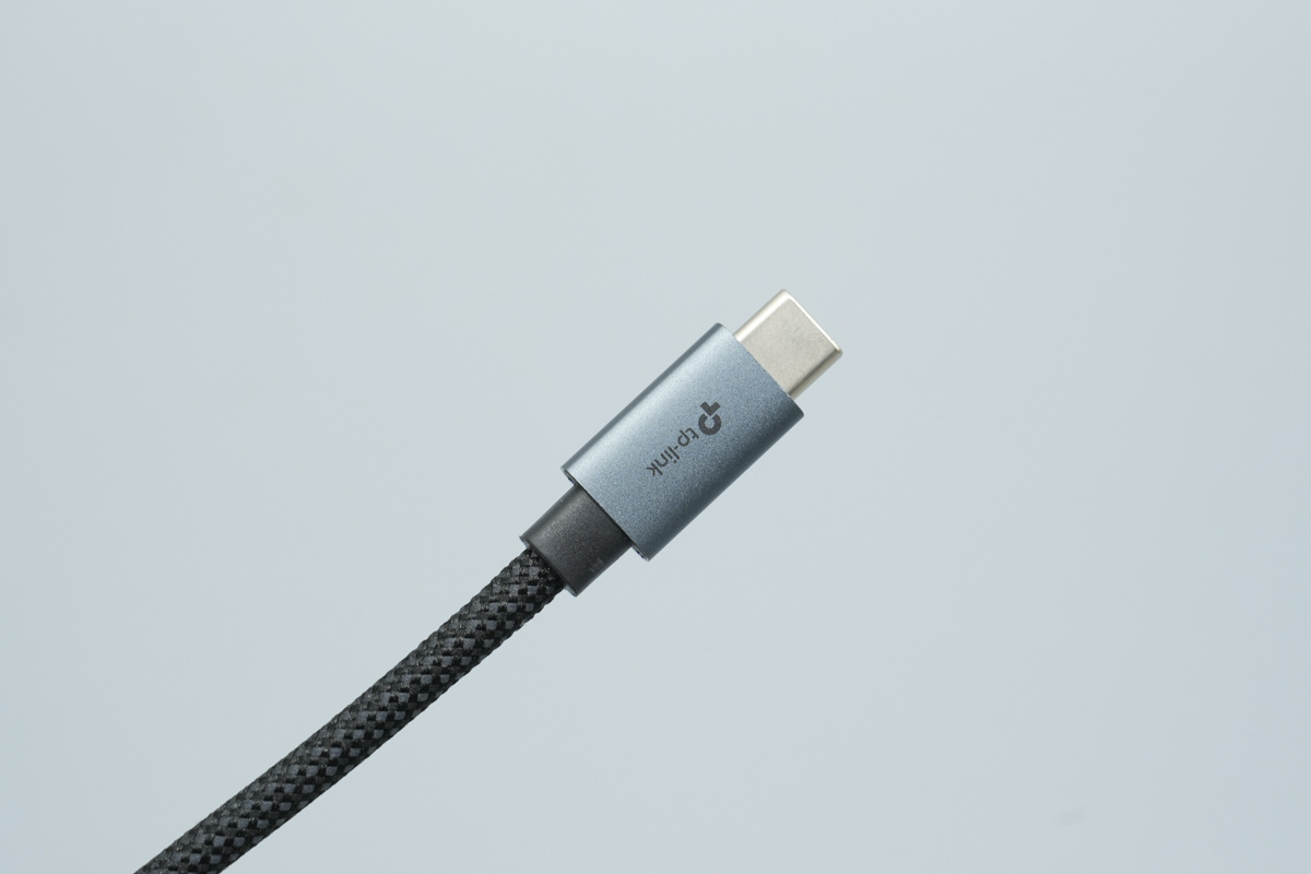
The USB-C connector sports the tp-link logo on its metallic exterior, paired with a robust nylon braided cable that provides excellent durability and resistance to pulling and fraying.
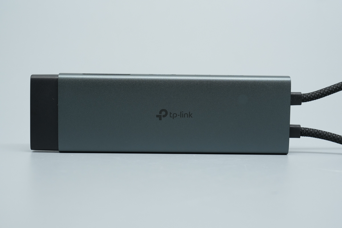
It features a minimalist, business-oriented design that prioritizes clean lines and simplicity.
The dock sports a stylish two-tone look, contrasting light gray and space gray for a modern, high-end feel.
The front-facing tp-link logo is laser-etched for superior durability and wear resistance.
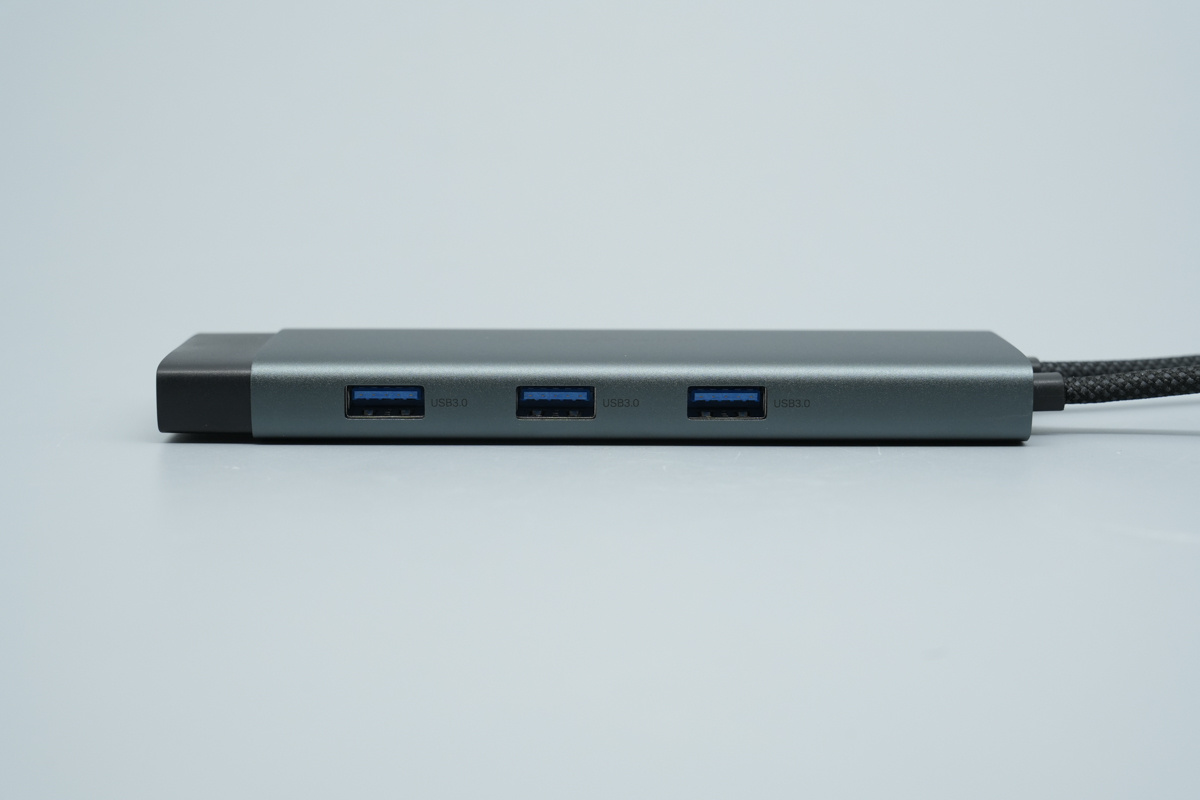
The side of the chassis houses three USB-A 3.0 data ports, distinguished by their blue internal plastic sheet.
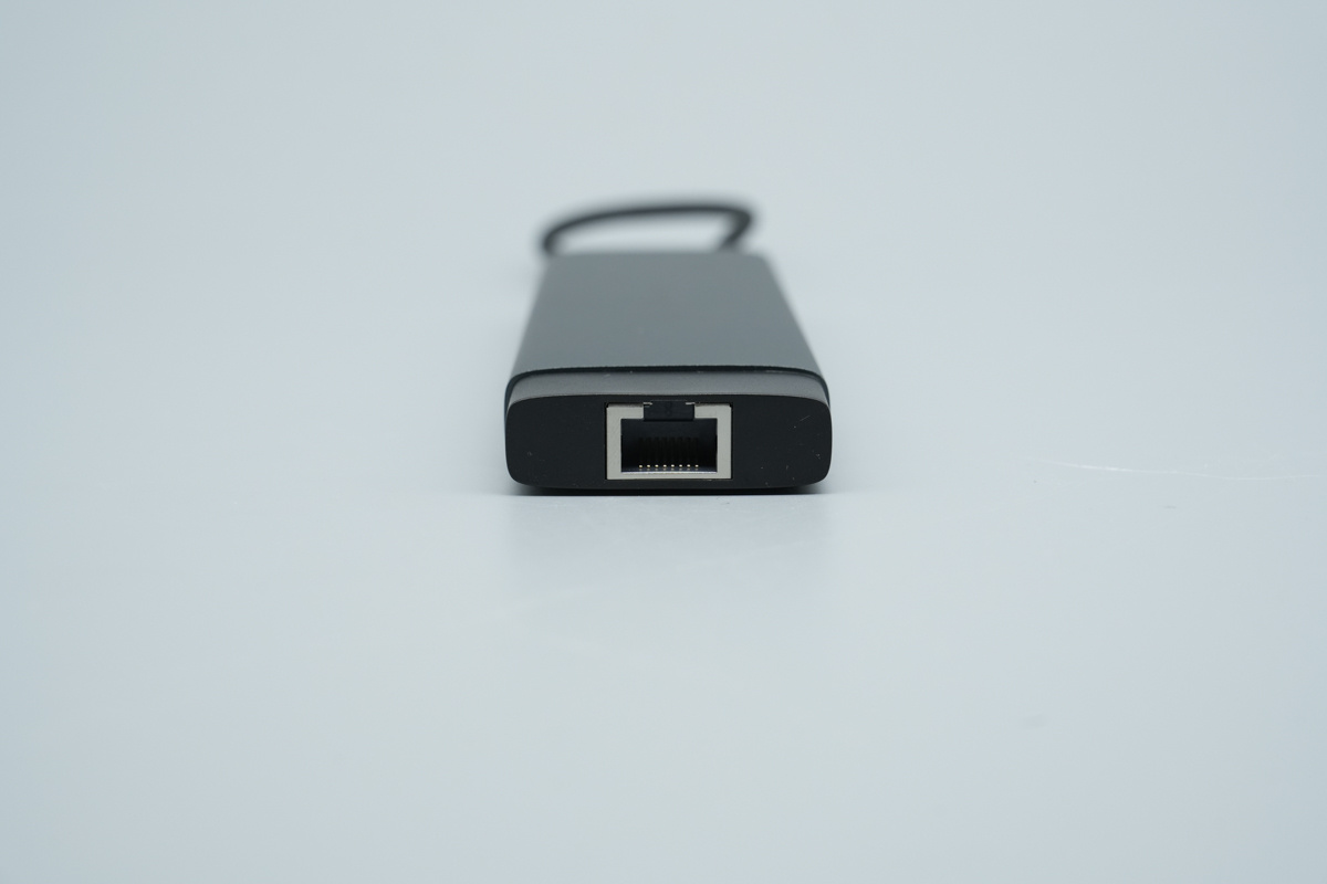
The top surface features an RJ45 Gigabit Ethernet port, ensuring reliable high-speed wired internet access.
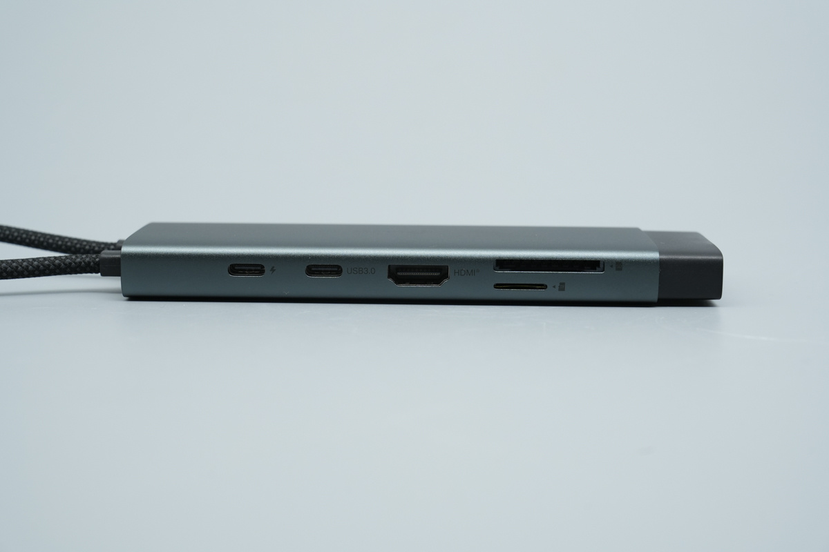
The other side includes a full suite of essential ports: a USB-C PD input, a USB-C data port, an HDMI video port, and dual SD/TF card slots.
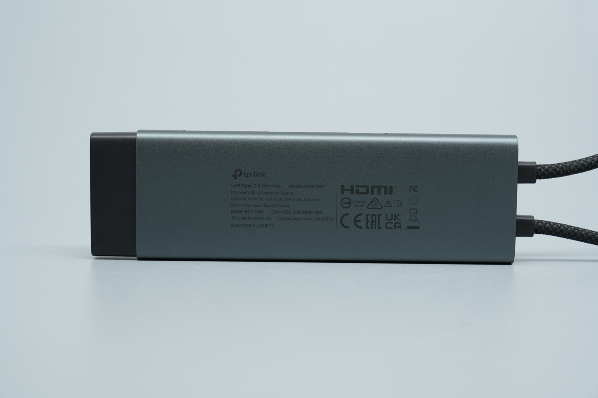
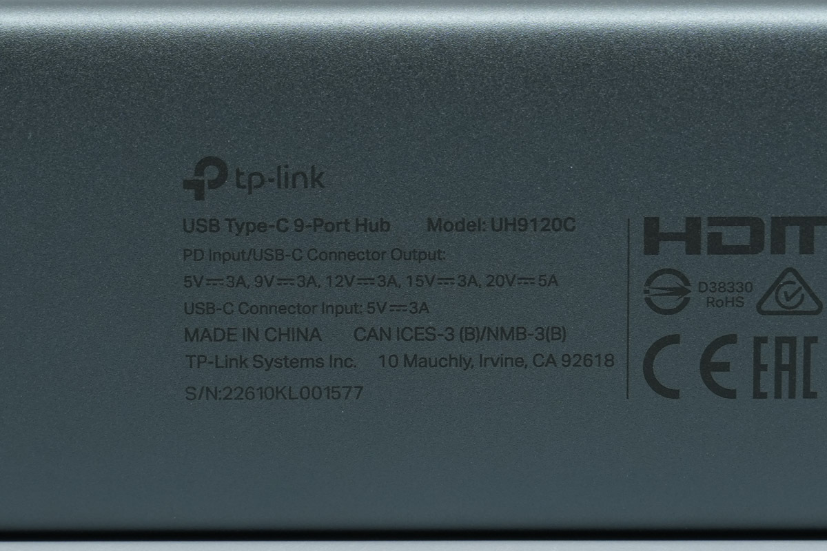
The rear of it is laser-etched with comprehensive technical specs and mandatory safety certifications.
Product Data:
Model: UH9120C
Power Delivery: Input/Output supports 5V/3A, 9V/3A, 12V/3A, 15V/3A, 20V/5A
Origin: Made in China
Certifications: CE, EAC
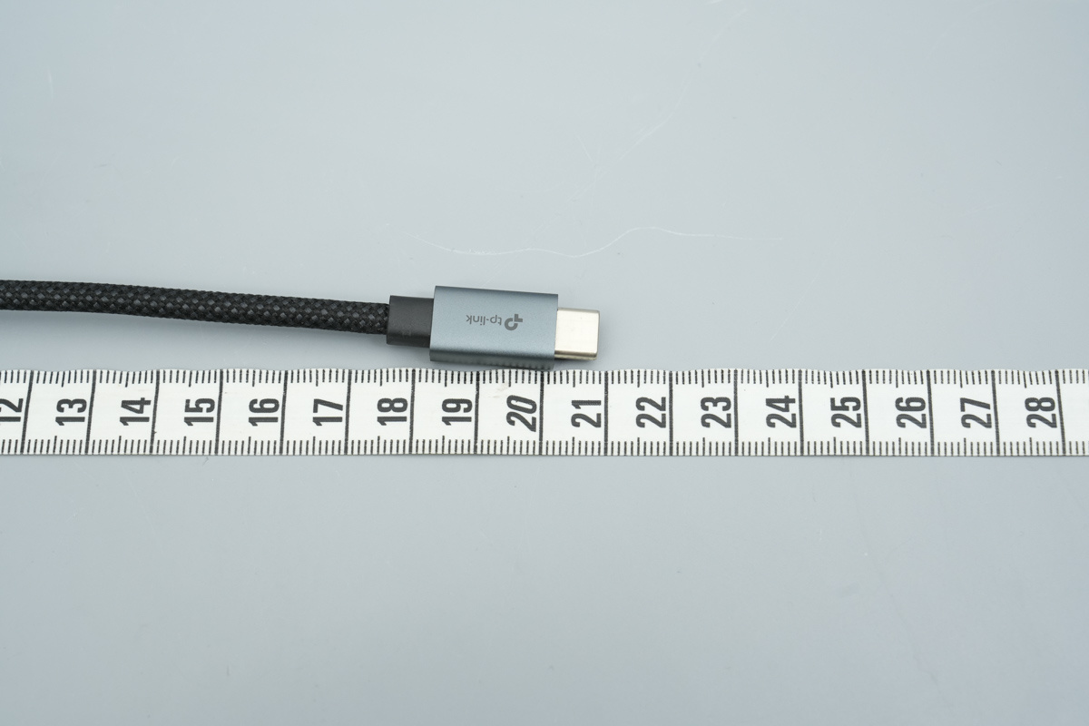
The length of the integrated cable is approximately 18–20cm.
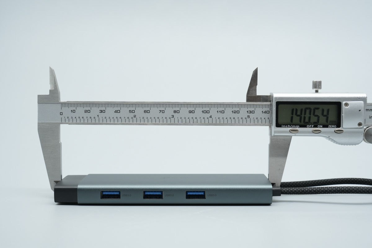
The length of the dock is about 140.54mm (5.533 inches).
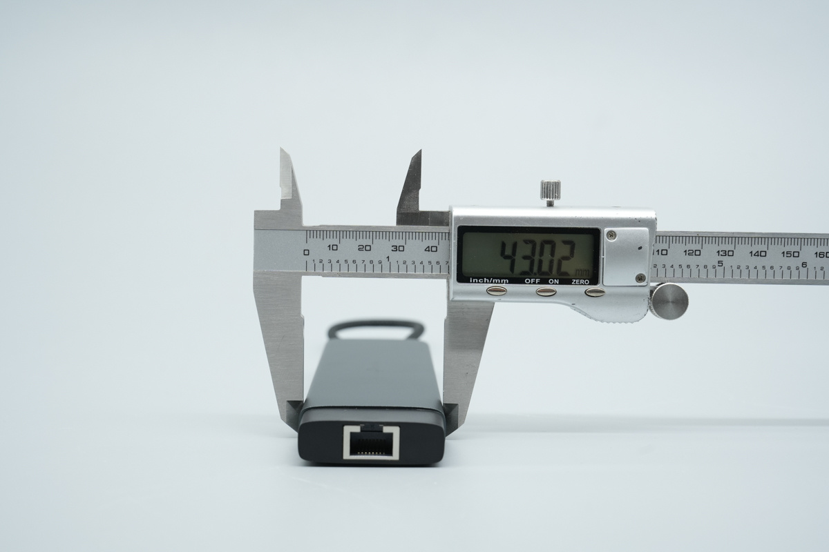
The width of the dock is about 43.02mm (1.694 inches).
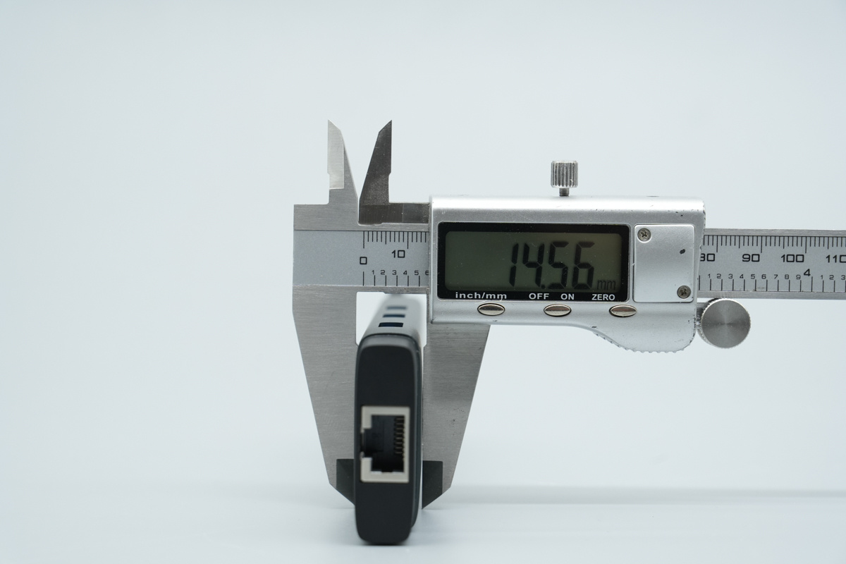
The thickness of the dock is about 14.56mm (0.573 inches).
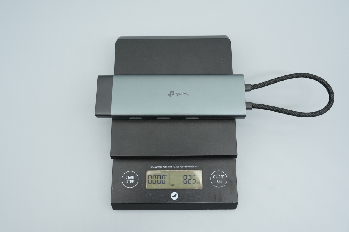
The weight is about 82.5g (2.91 oz).
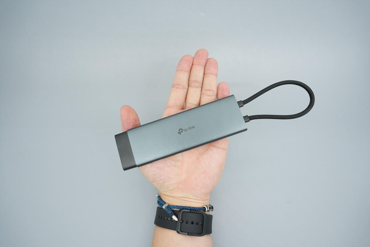
That's how big it is in the hand.
Now that we’ve wrapped up our quick look at the design, let's diving straight into the full internal teardown.
Teardown
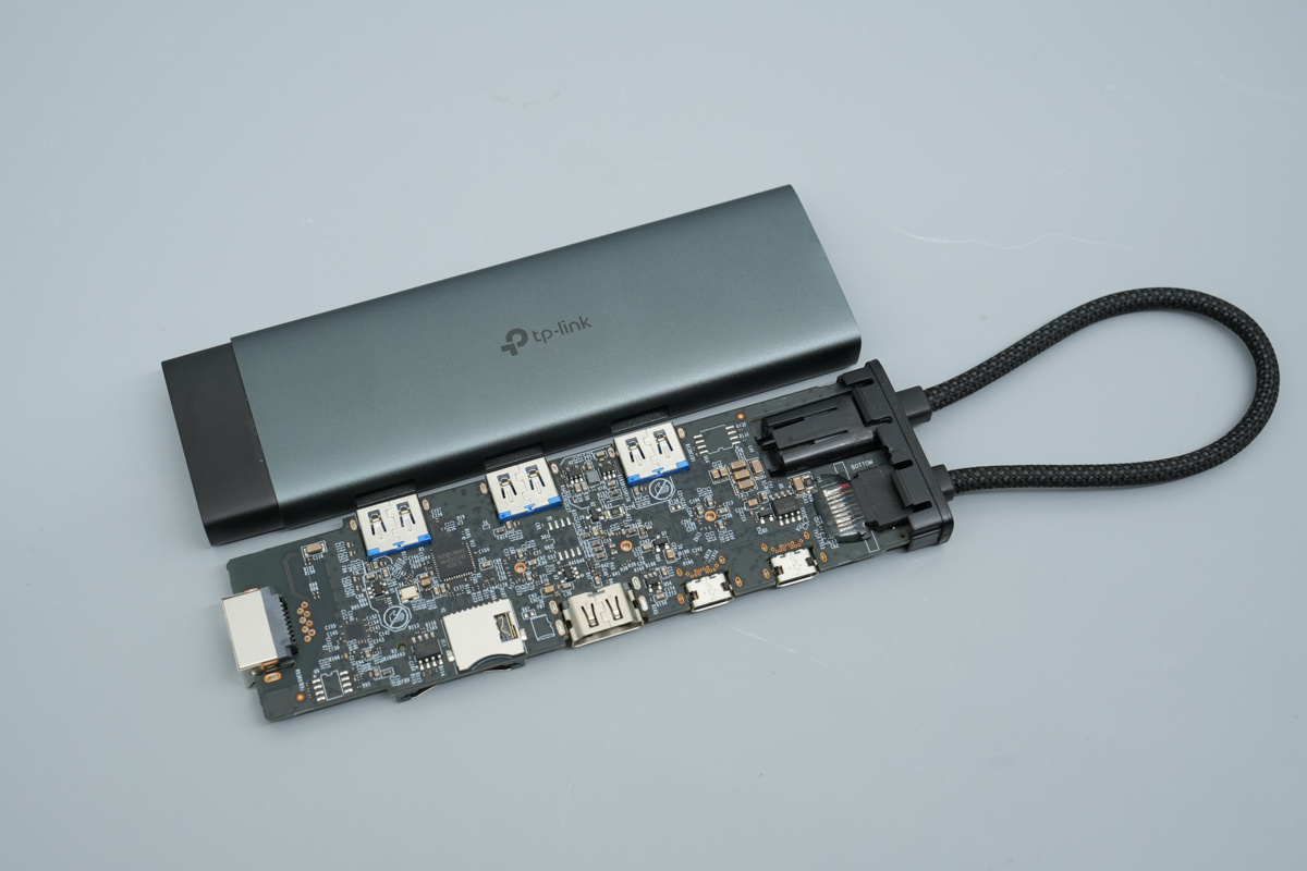
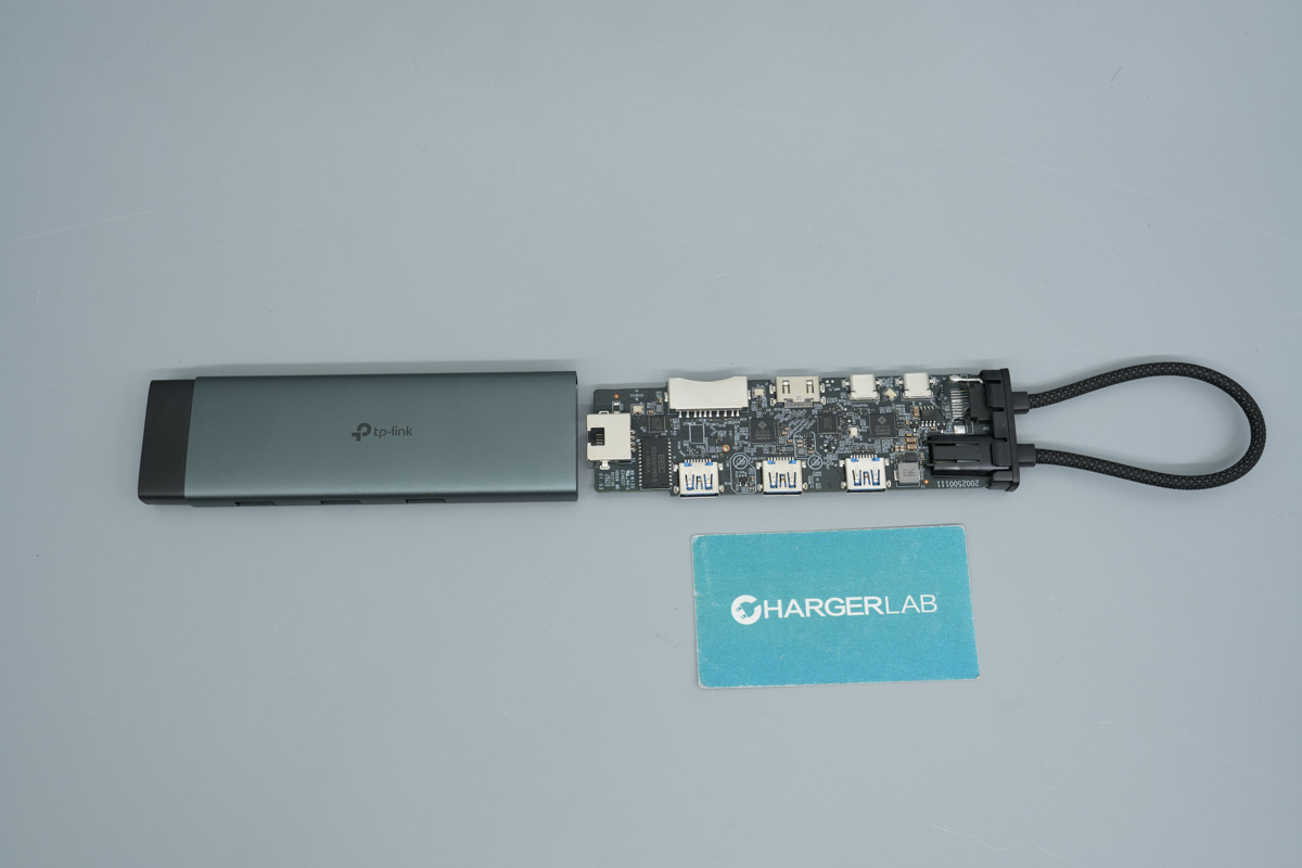
Removing the PCBA reveals that the chassis interior utilizes snap-fit clips on both sides to keep everything locked perfectly in place.
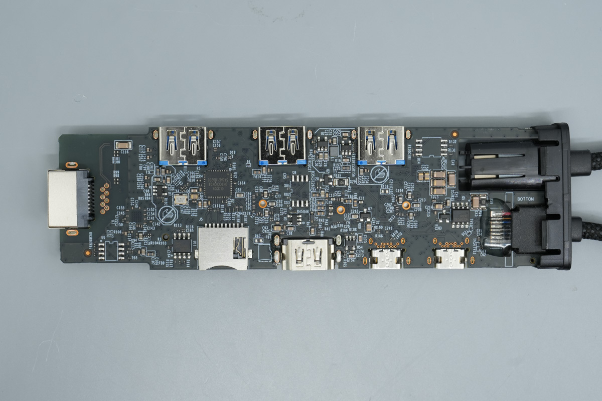
The top of the PCBA houses the card reader chip, the memory chip, and the VBUS MOSFETs, showcasing a highly integrated design.
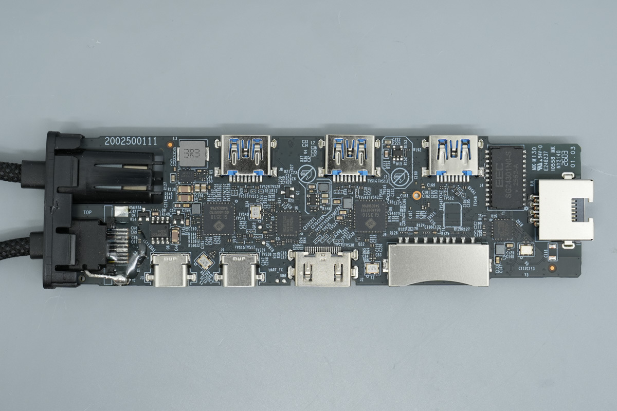
The back of the PCBA houses the USB HUB controller, the video conversion chip, and the network isolation transformer.
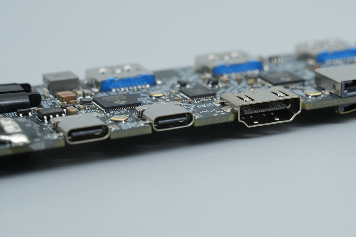
The side houses two USB-C ports with black plastic sheets, one for PD power delivery input and one for USB 3.1 data transmission.
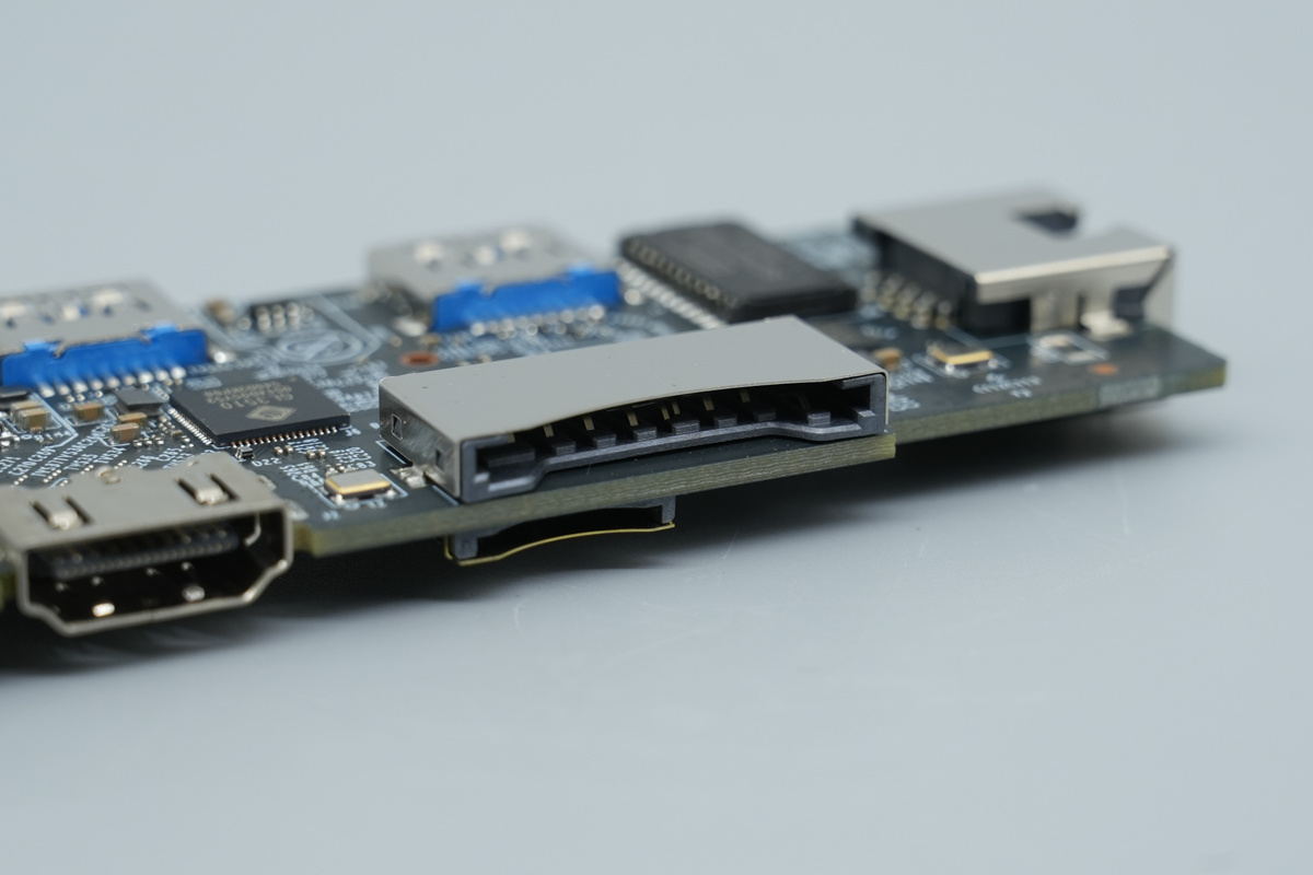
There is an HDMI video port, and integrated slots for SD and TF memory cards.
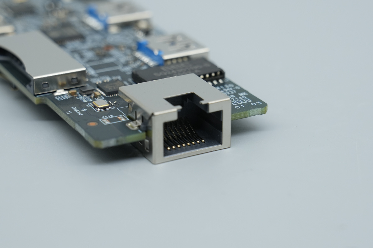
The PCBA features a RJ45 Gigabit Ethernet port integrated on its side.
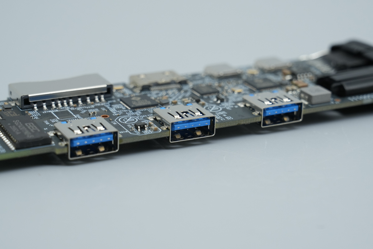
The other side features three USB-A 3.0 ports, all distinguished by their blue plastic sheets.

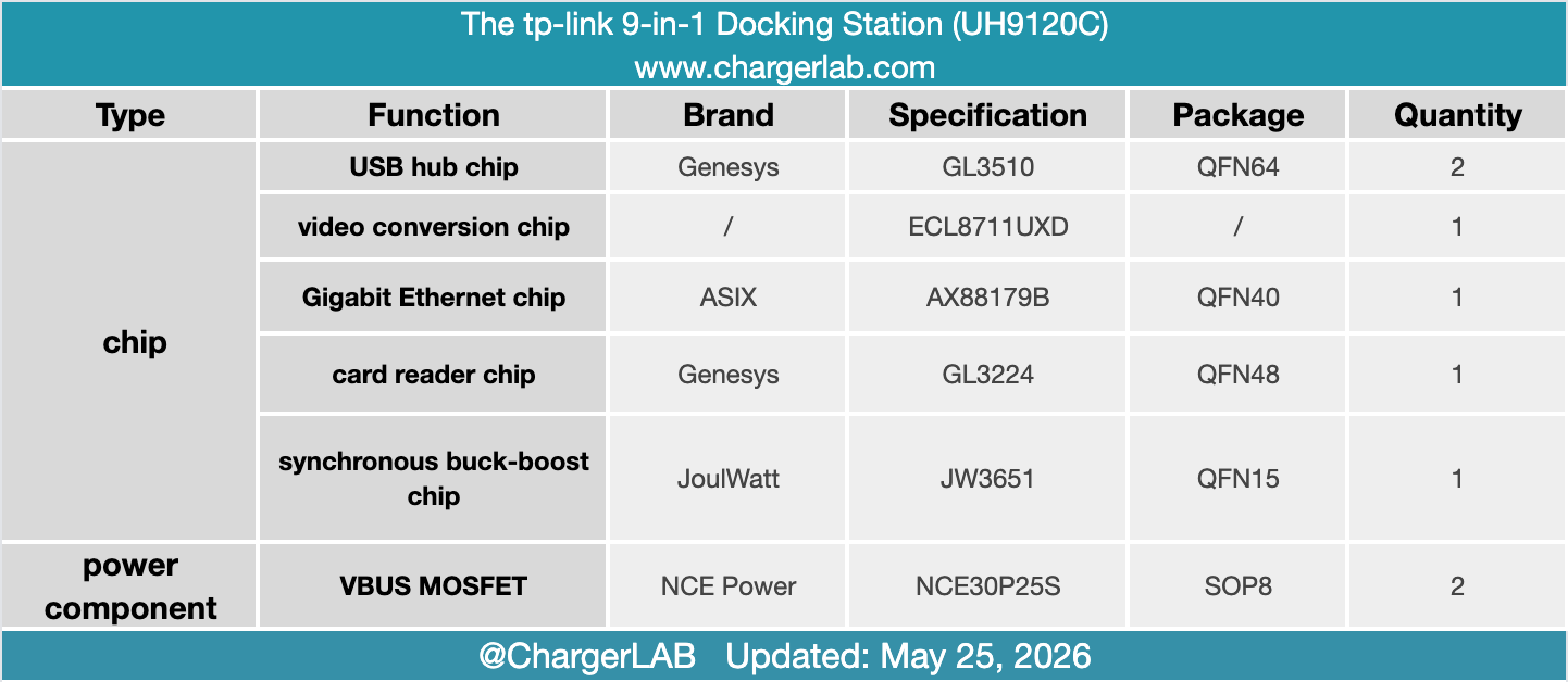
The synchronous buck-boost chip is from JoulWatt, model JW3651. It features a single-choke architecture, supporting output voltages up to 20V. It offers robust versatility by maintaining stable output regulation across input voltages that are equal to, lower than, or higher than the target output voltage.
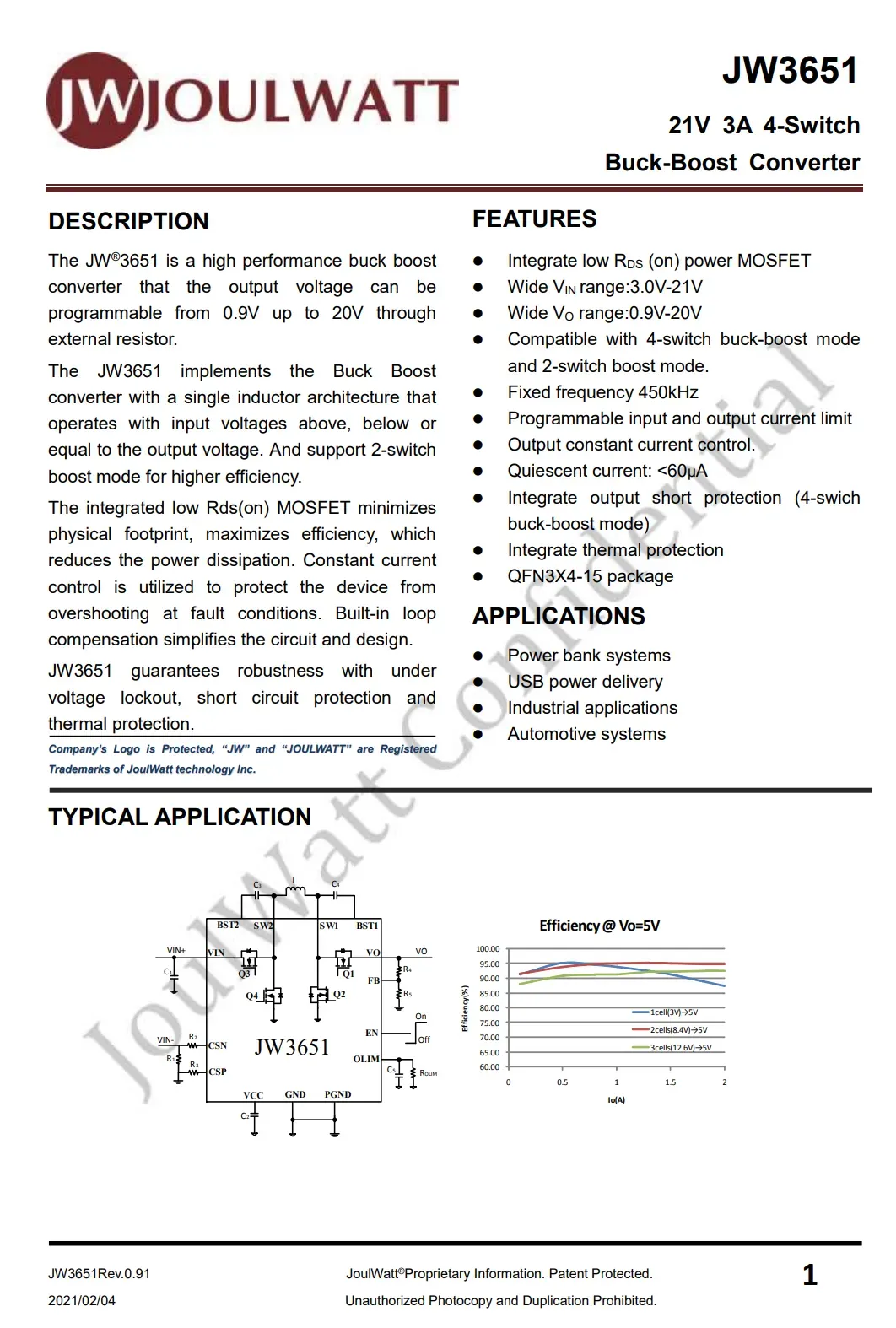
It integrates four MOSFETs within a compact architecture to minimize PCB footprint and optimize energy efficiency. Key features include:a 450kHz switching frequency, programmable output voltage and current limiting, constant current control, output short-circuit protection, and thermal shutdown functionality, all housed in a space-saving QFN3x4-15 package.
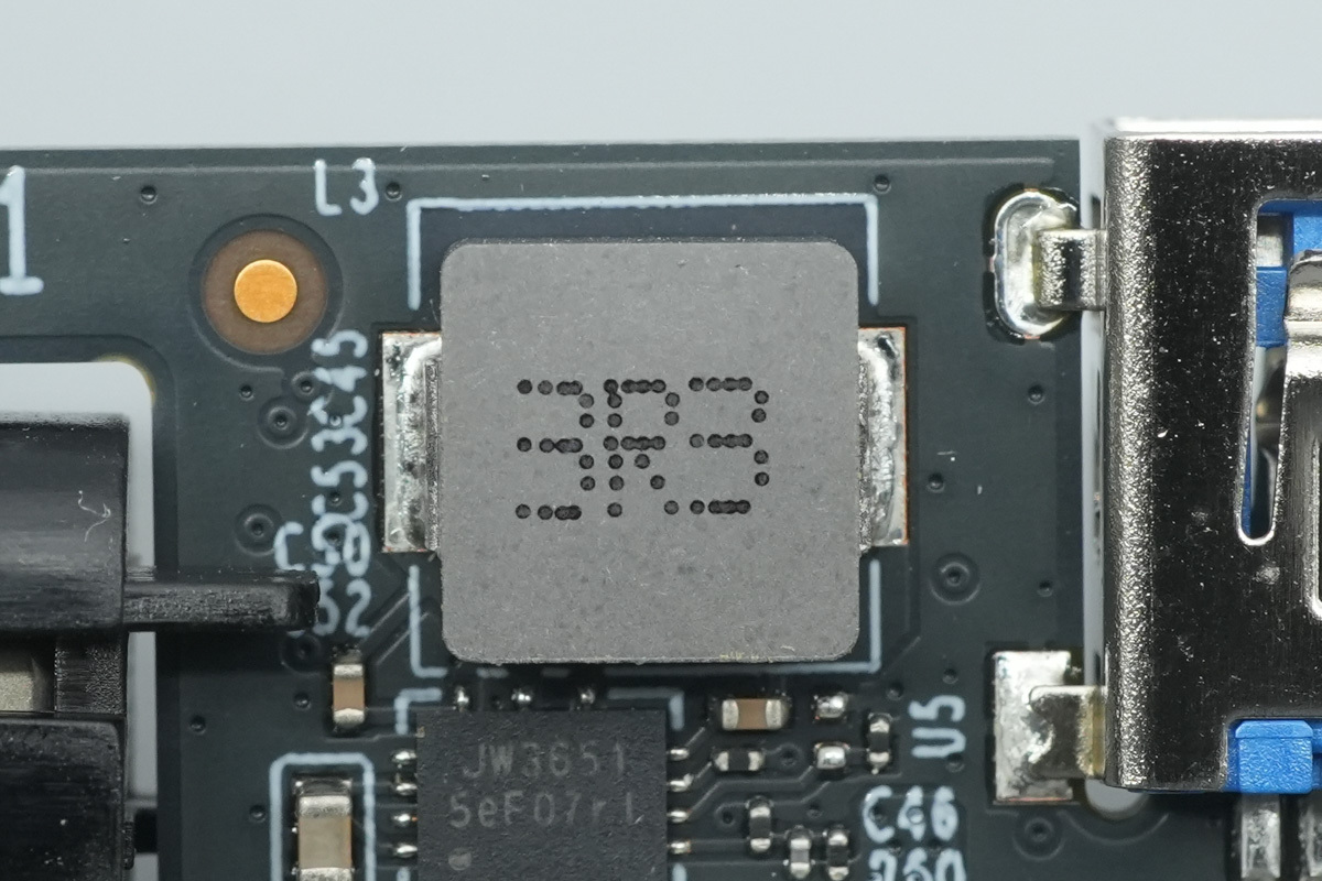
This is a metal alloy choke from JoulWatt, model JW3651.
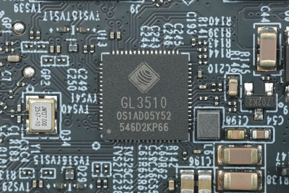
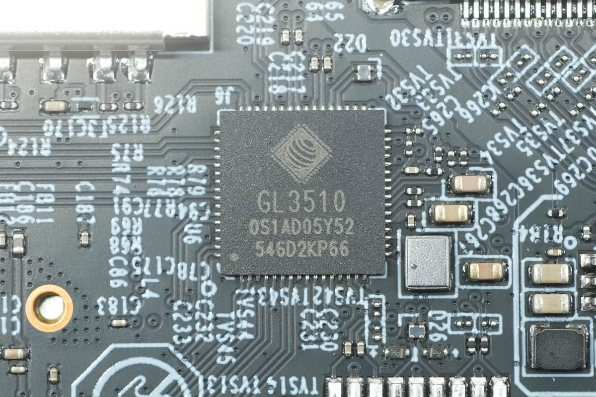
The USB hub chip is from Genesys, model GL3510, in a QFN64 package. This four-port, low-power chip supports USB 3.0 while maintaining full backward compatibility with USB 2.0, and features an integrated switching voltage regulator. It facilitates USB 3.0 expansion, driving the three USB-A ports and the downstream GL3510.
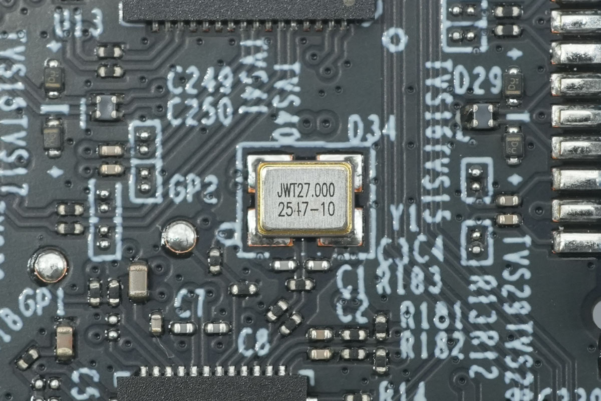
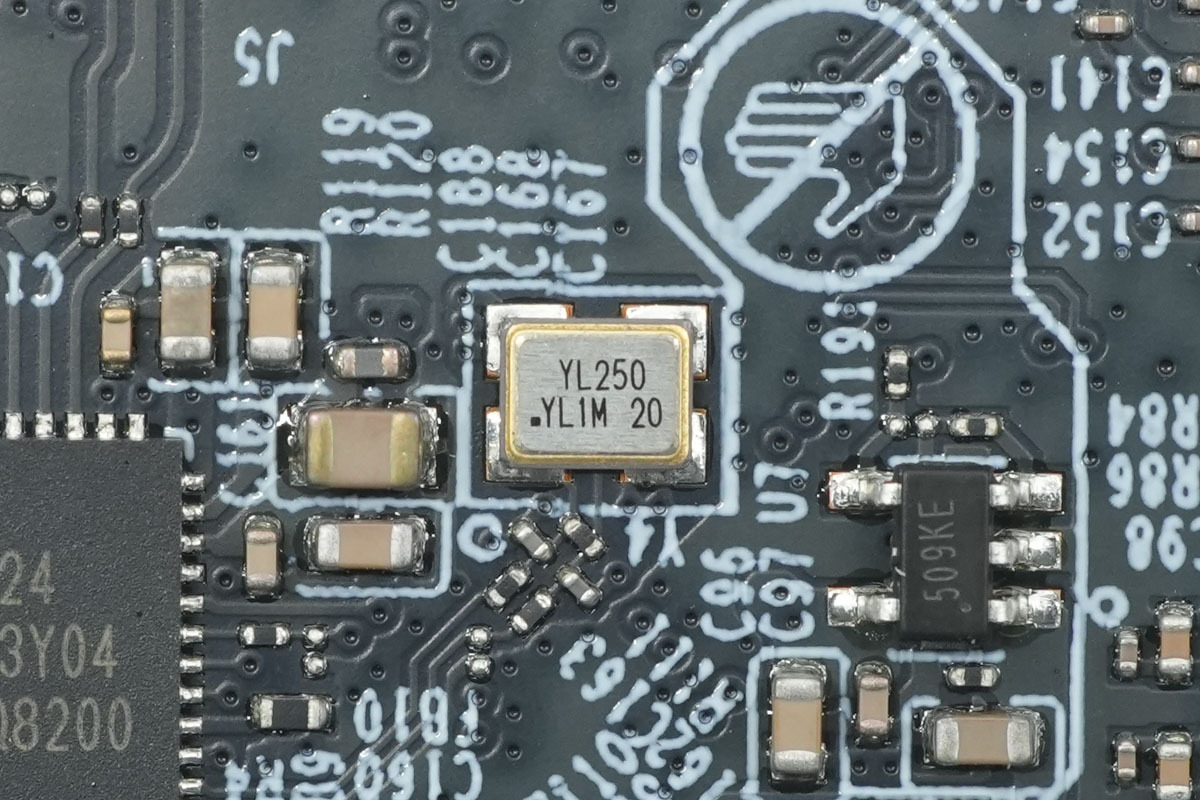
A crystal oscillator is located alongside the USB hub chip.
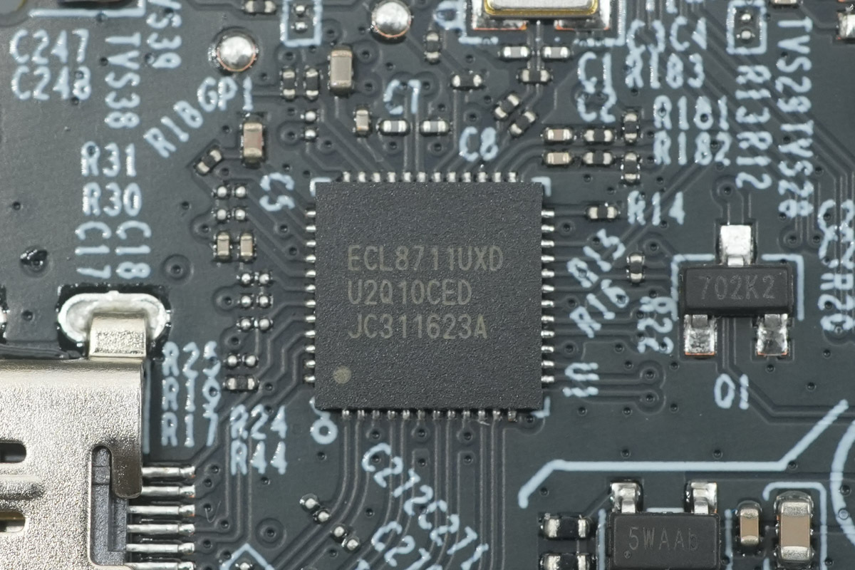
A control chip, marked ECL8711UXD, is for HDMI output conversion.

A chip, marked 5WAAb.
The dock features a second USB hub chip, also from Genesys, model GL3510.
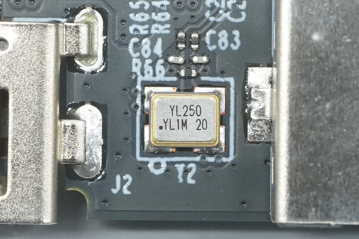
Another crystal oscillator is located nearby.
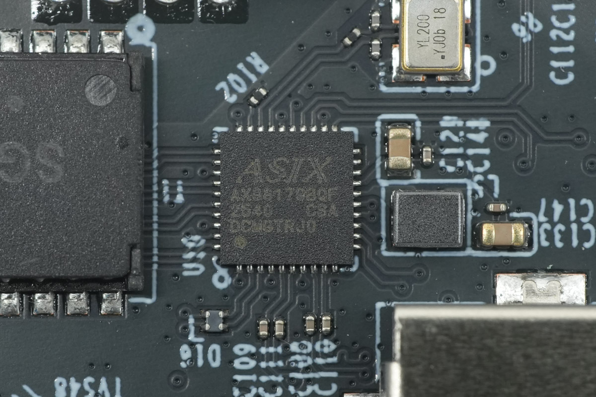
A Gigabit Ethernet chip is from ASIX, model AX88179B.
芯片旁还设有一颗晶振。
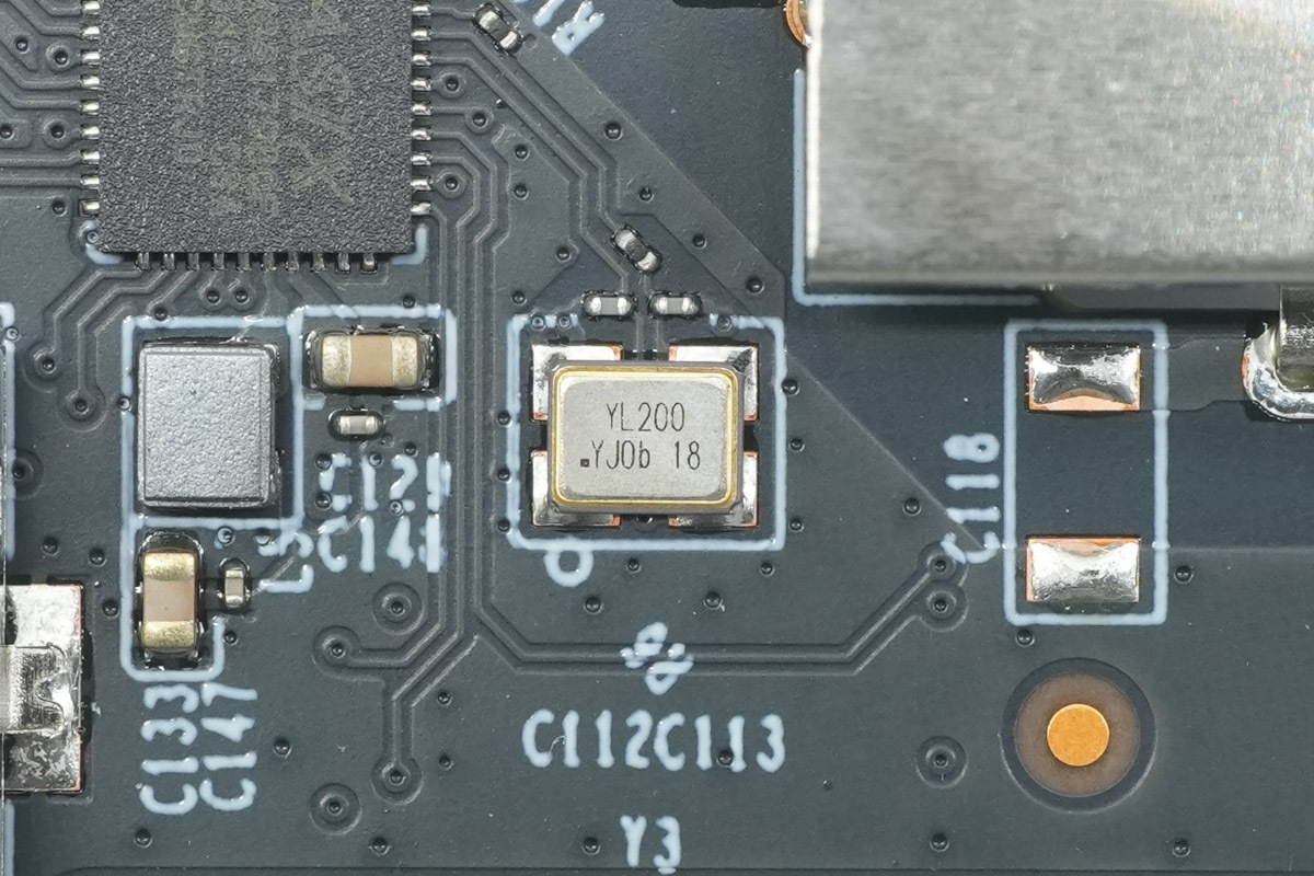
A crystal oscillator is located next to the chip.
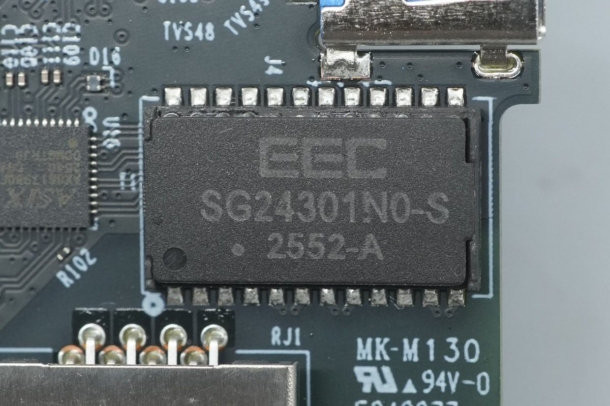
Behind the RJ45 port, features an network isolation transformer, model SG24301N0-S.
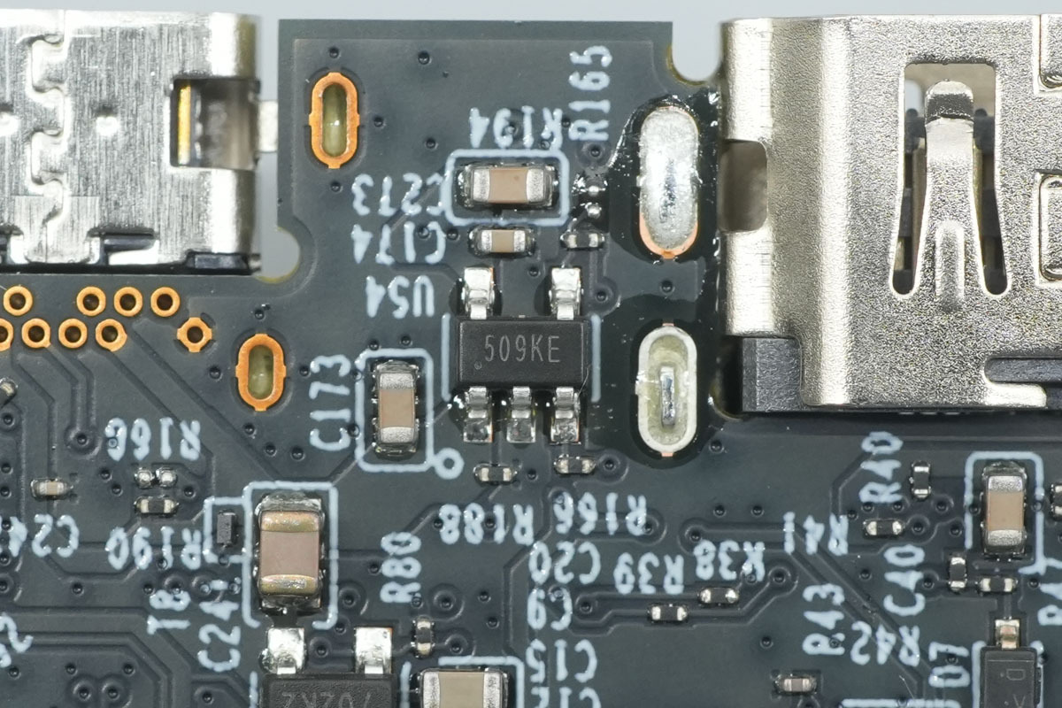
A chip, marked 509KE.
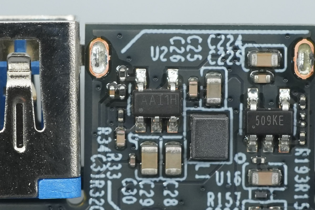
A chip, marked AA1H.
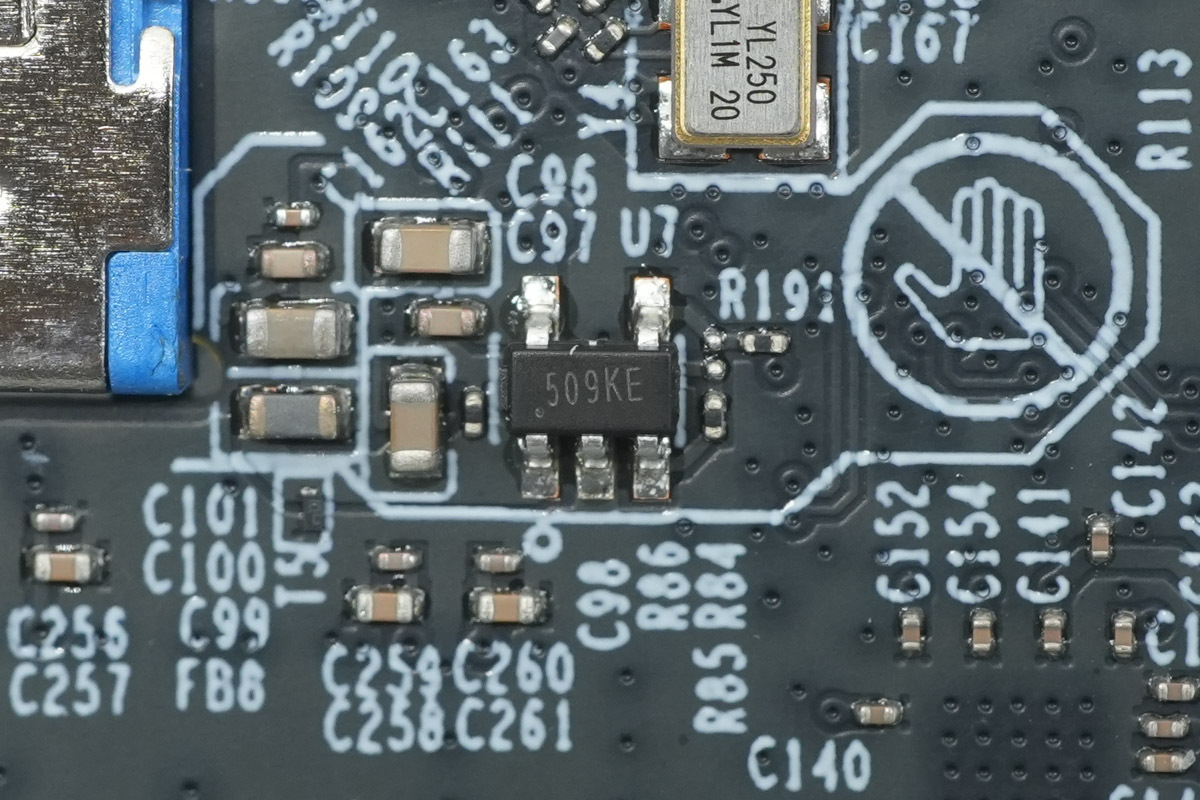
Another chip, marked 509KE.
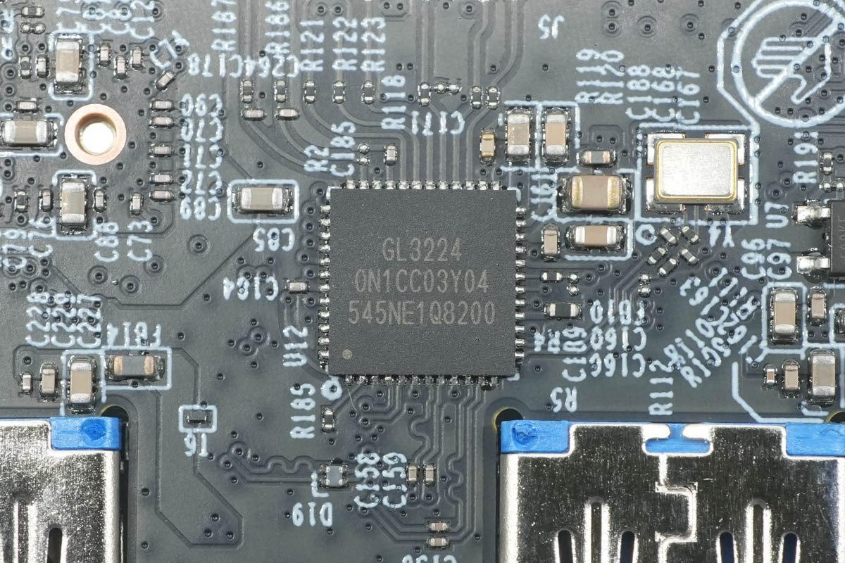
The card reader chip is from Genesys, model GL3224, and in a QFN48 pakage, which provides high-speed read/write support for both SD and MicroSD memory cards.
A crystal oscillator is paired with the Genesys Logic GL3224 chip.
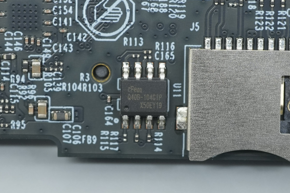
The memory chip is from cFeon, model Q40B-104GIP NOR Flash.
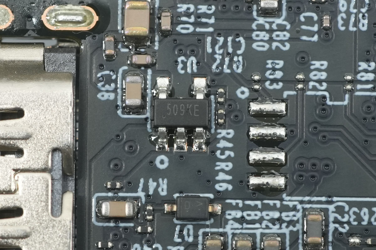
A chip, marked 509KE.
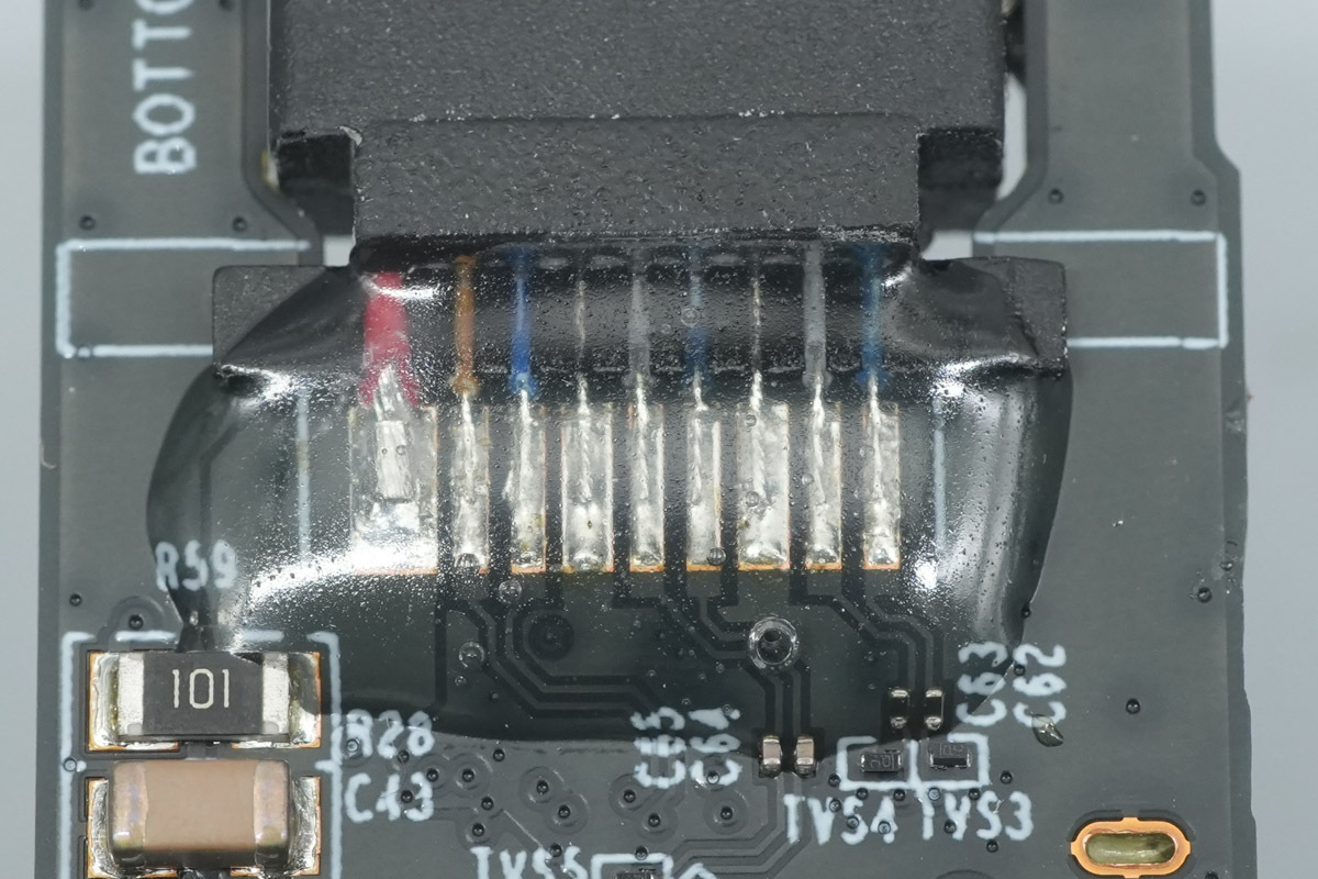
The integrated USB-C cable is neatly soldered to the PCBA, with the connection point encapsulated in hard potting compound for mechanical reinforcement and insulation.
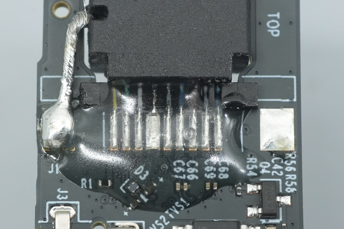
On the back of the main PCB, the cable solder joints are similarly encapsulated with a substantial, high-density hard potting compound, ensuring structural stability and increased product longevity in daily operation.
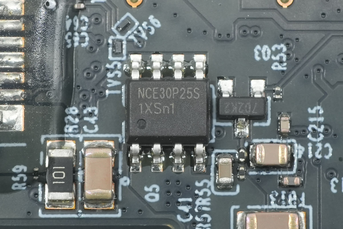
The VBUS MOSFET is from NCE, model NCE30P25S, PMOS, -30V and 9mΩ, and in a SOP8 package.
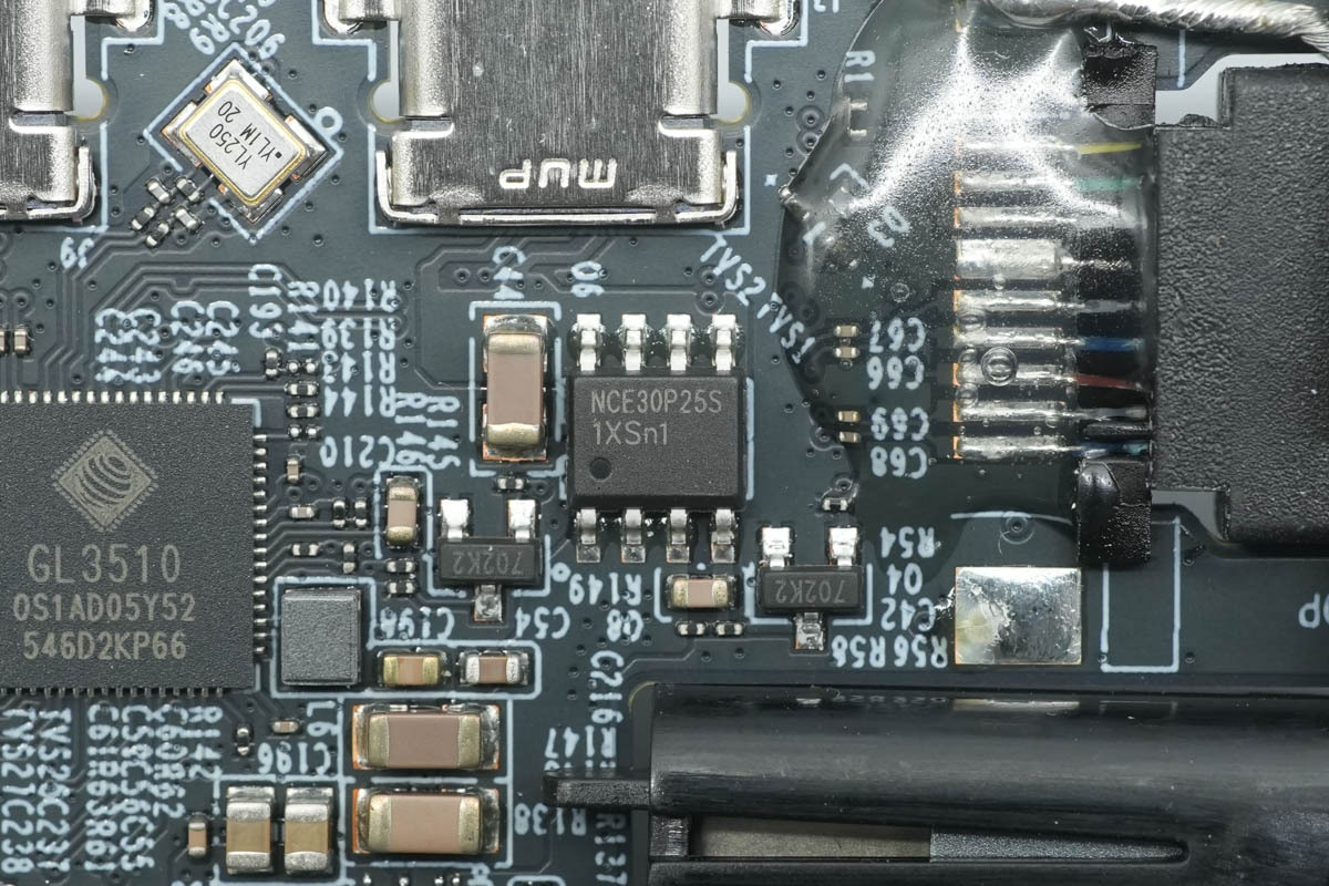
Another one is also from NCE, model NCE30P25S.
Well, those are all components of the tp-link 9-in-1 docking station.
Summary of ChargerLAB
Wrapped in a sleek space-gray aluminum shell, the tp-link 9-in-1 docking station blends excellent heat dissipation with a professional look.
The real highlight is the cable self-storage design. By docking the USB-C plug into the rear of the device, you create a convenient carry loop—an elegant solution that protects your gear from accidental scratches.
Internally, the dock is engineered for reliability. It relies on the Genesys GL3510 and GL3224 chips for data and card management, paired with the battle-tested ASIX AX88179BQF chip for high-speed Ethernet, complete with an the network isolation transformer.
The build quality is exceptional, featuring extensive hard potting compound on the cable connections to ensure maximum longevity, cementing its status as a top-tier flagship peripheral.
Related Articles:
1. Teardown of Anker Prime 14-in-1 Docking Station (A83B3) – Black Myth: Wukong Edition
2.HP Unveils Thunderbolt 4 Ultra G6 Dock at CES 2025
3. Razer Unveils Powerful USB 4 Docking Station for Ultimate Connectivity and Productivity