Introduction
Beyond its profound expertise in the gaming smartphone sector, Nubia has executed a systematic strategic layout for its peripheral accessory ecosystem lately.
Evolving from early bundled fast-chargers to the now fan-favorite DAO Series, It has carved out a unique brand identity in the crowded fast-charging market with its bold design DNA.
Previously, ChargerLAB has conducted in-depth reviews and teardowns of dozens of power products under both the Nubia and REDMAGIC brands.
ChargerLAB has just got its hands on Nubia’s latest 45W single USB-C charger. The design stays true to the brand's sleek, compact aesthetic, complete with that iconic signature red plastic sheet. Beyond its looks, It offers extensive utility by supporting PD, PPS, and multiple mainstream fast-charging protocols.
Stay tuned as we perform a deep-dive teardown to see what's powering this versatile charger from the inside.
Product Appearance
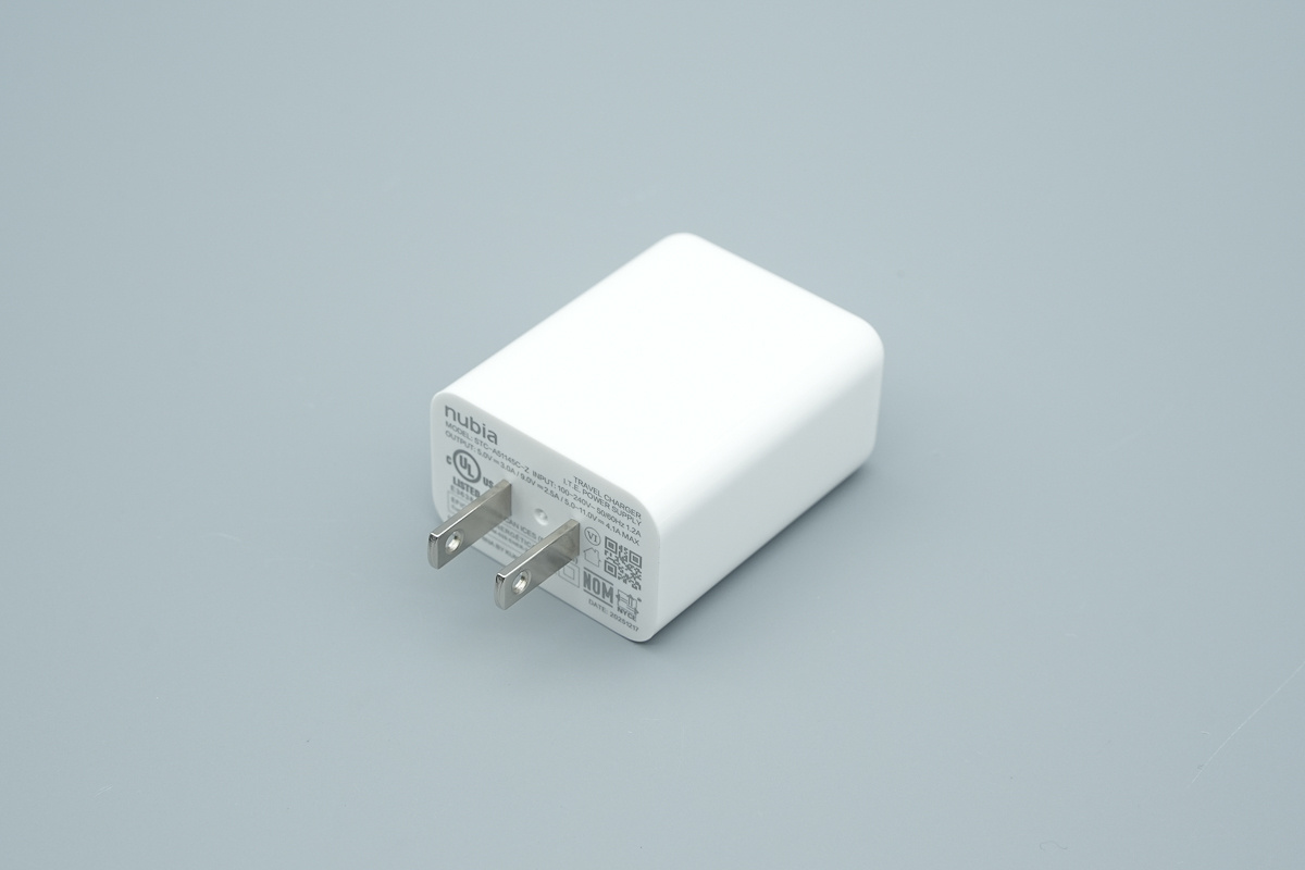
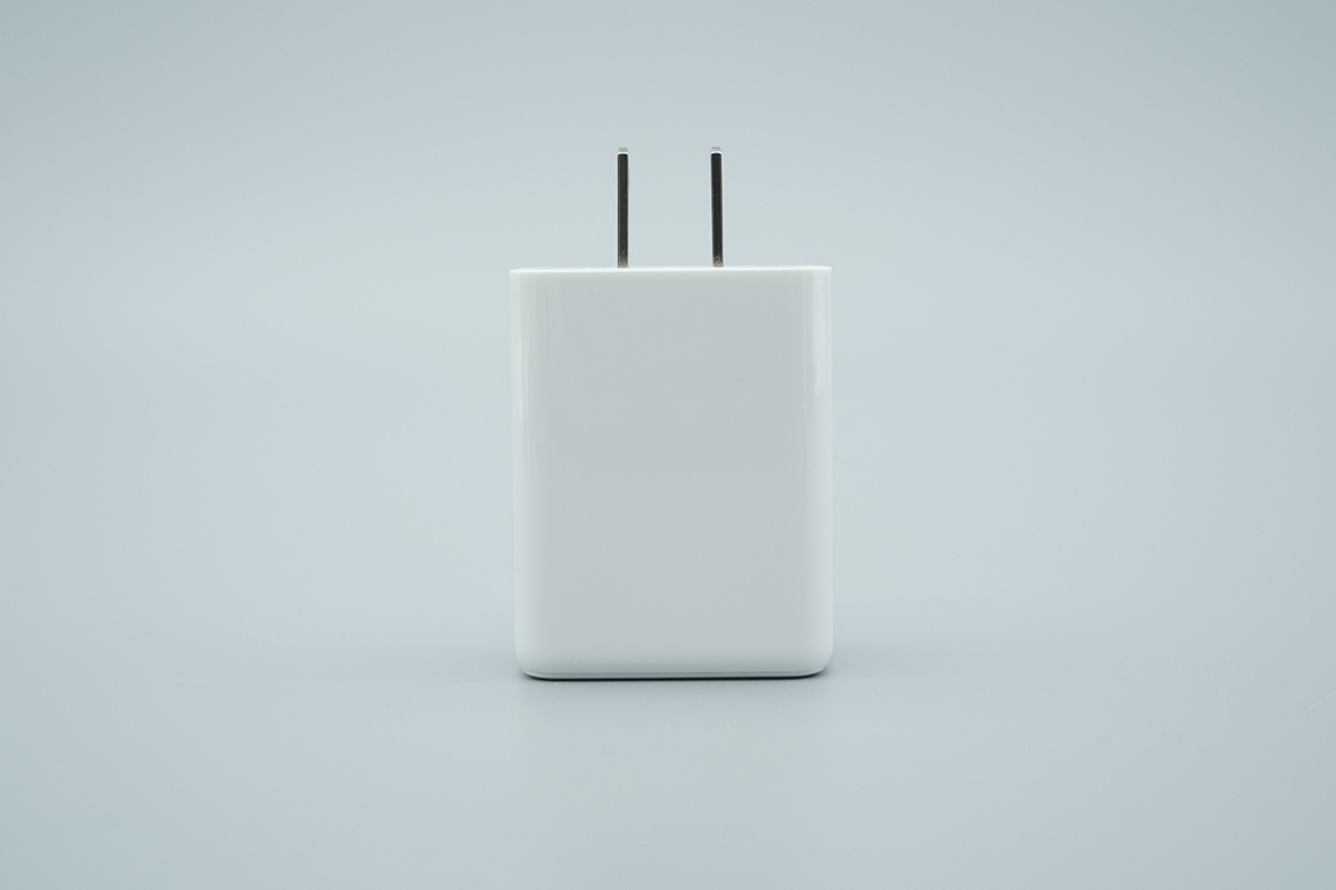
Designed with a sleek, pure white rectangular body, the charger boasts a clean and simple exterior.
The side panels of the housing feature smooth contoured transitions, with an exterior finished in a polished glossy material.
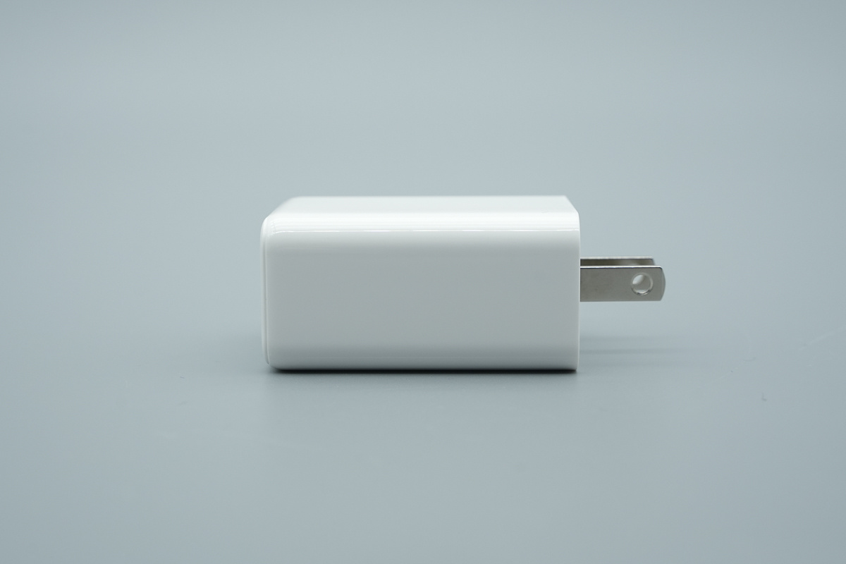
It features fixed US-standard prongs.
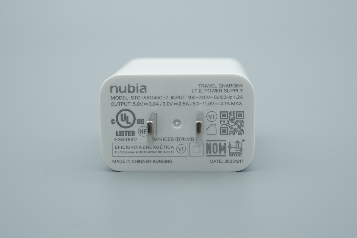
All detailed specs are neatly marked onto the base of it, right next to the prongs.
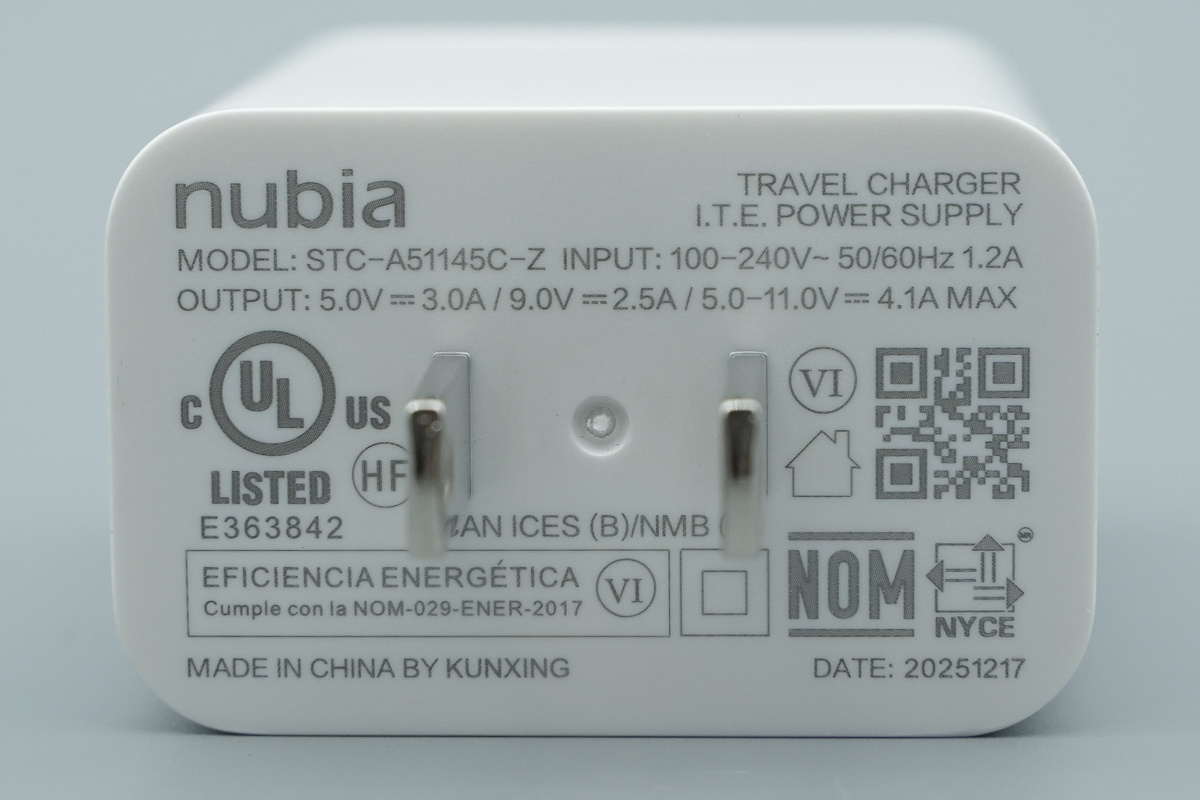
Nubia 45W Charger Nameplate Specifications:
Model: STC-A51145C-Z
Input: 100-240V~ 50/60Hz 1.2A
Output: 5.0V 3.0A / 9.0V 2.5A / 5.0-11.0V 4.1A MAX
Certifications: it has passed CULUS, NOM and NYCE certifications
Efficiency Standard: Features the Level VI energy efficiency certification mark
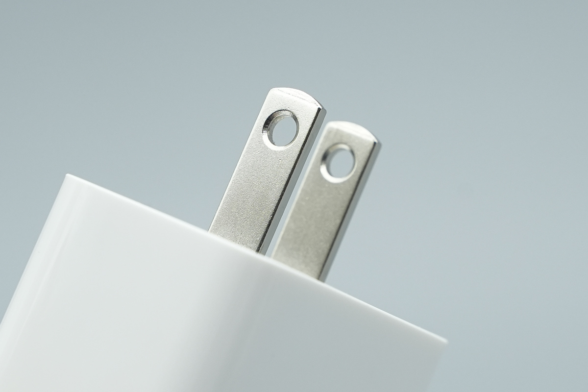
The AC metal prongs feature a nickel-plated surface finish and include the standard circular aperture design in compliance with US regulations.
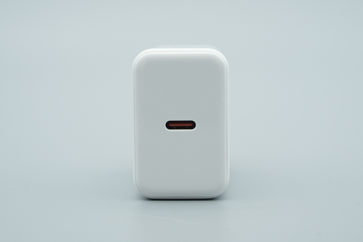
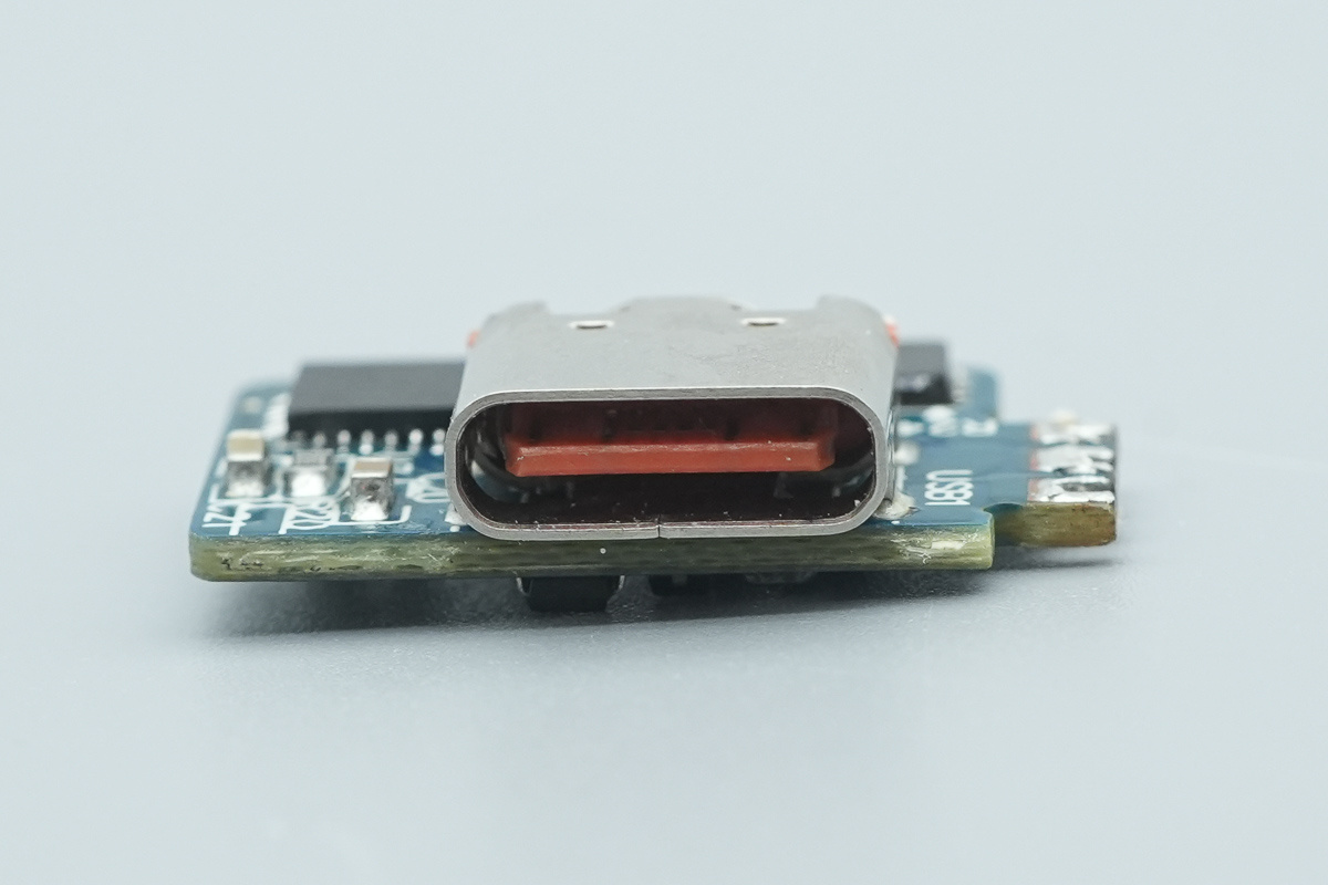
It features a single centered USB-C port on its output end. Inside, the signature red plastic sheet stands out, providing a high level of brand recognition.
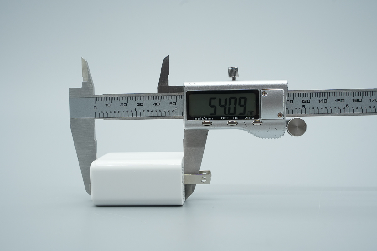
The length of the charger is about 54.09mm (2.130 inches).
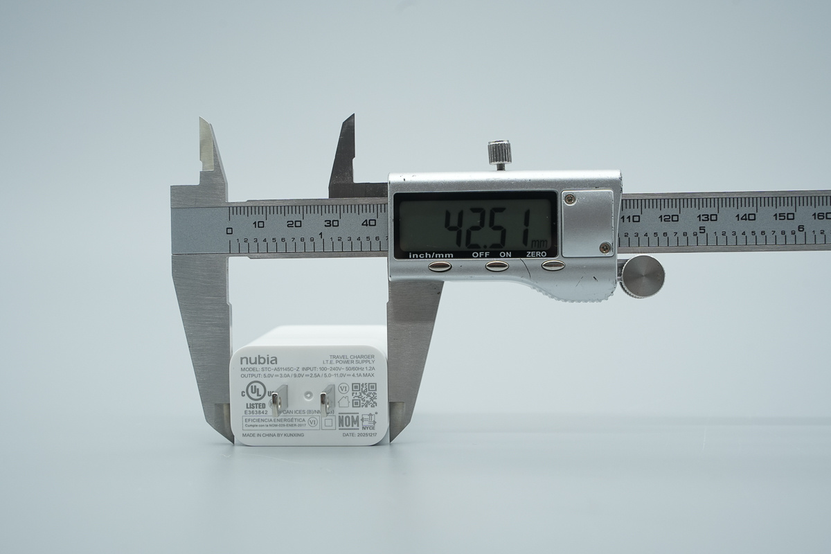
The width of the charger is about 42.51mm (1.674 inches).
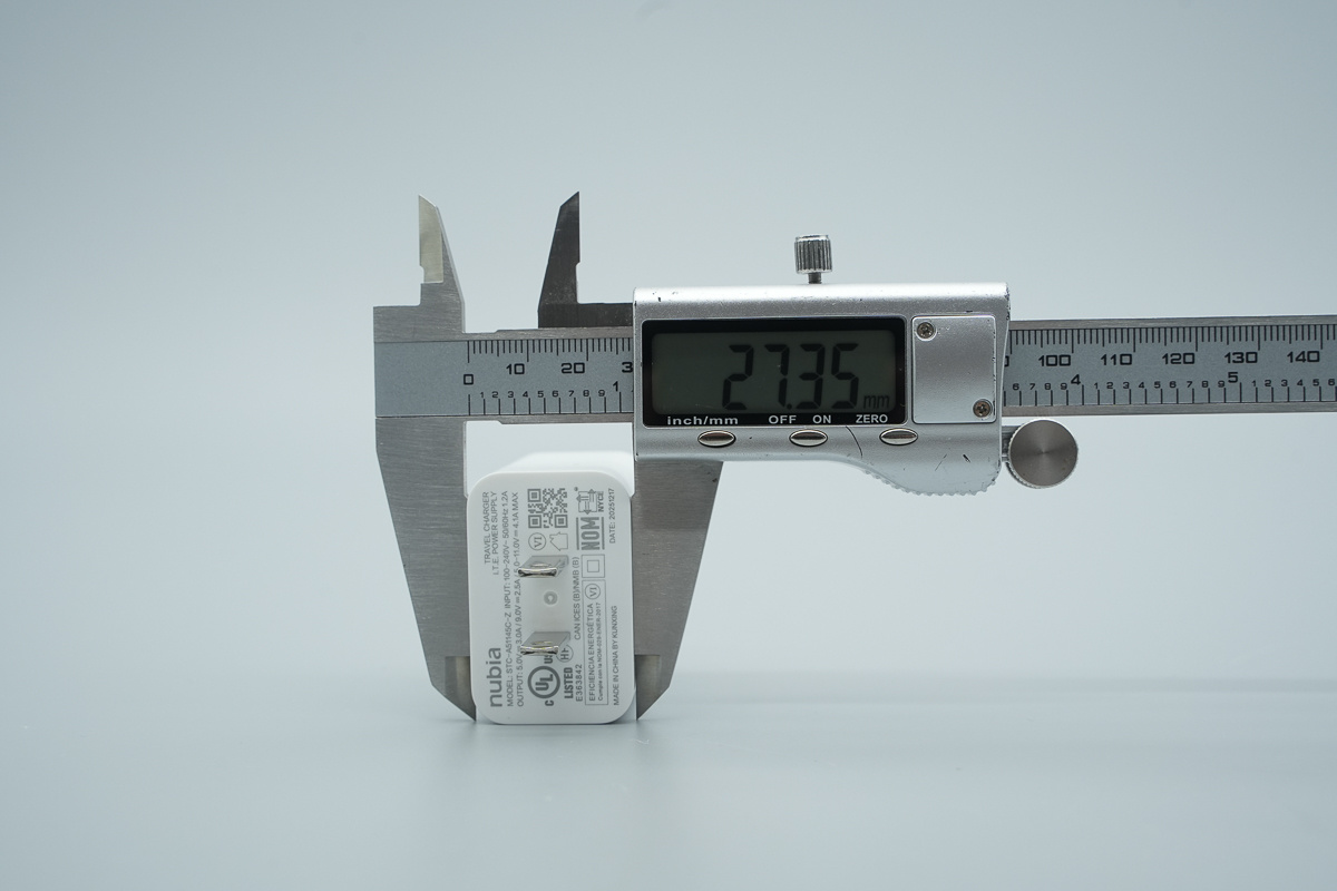
The thickness of the charger is about 27.35mm (1.077 inches).

The weight is about 71.7g (2.53 oz).
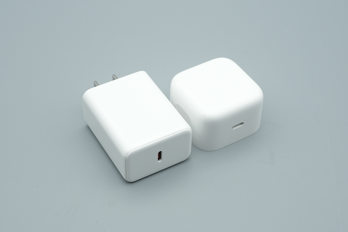
Put it with Apple’s 40W dynamic charger, it is remarkably similar.
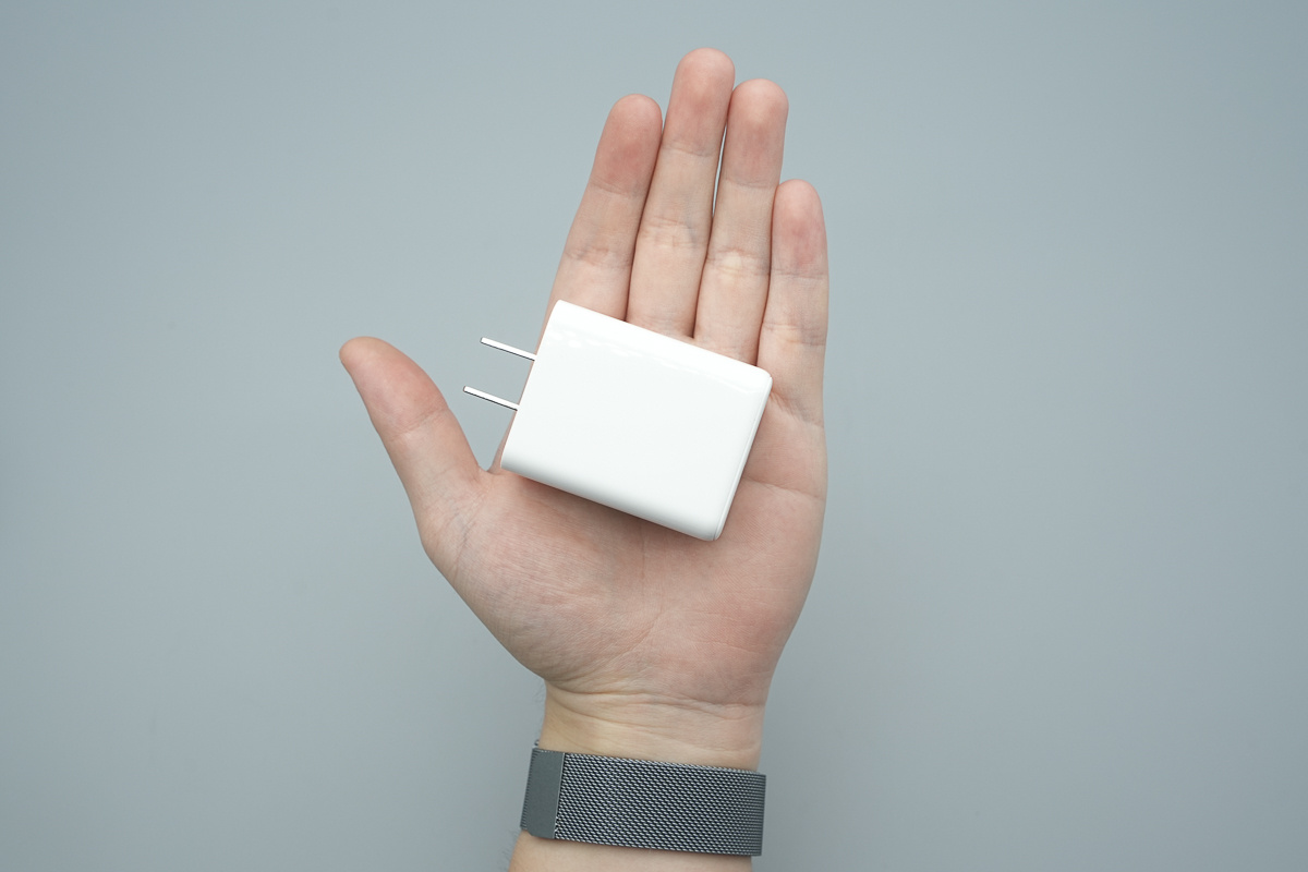
That's how big it is in the hand.
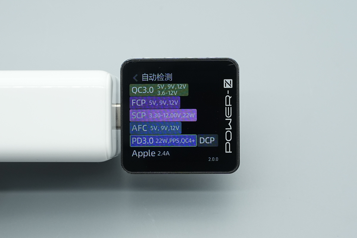
ChargerLAB POWER-Z KM003C shows that the USB-C port supports QC3.0, FCP, SCP, AFC, PD3.0/PPS, QC4+, Apple 2.4A and DCP.
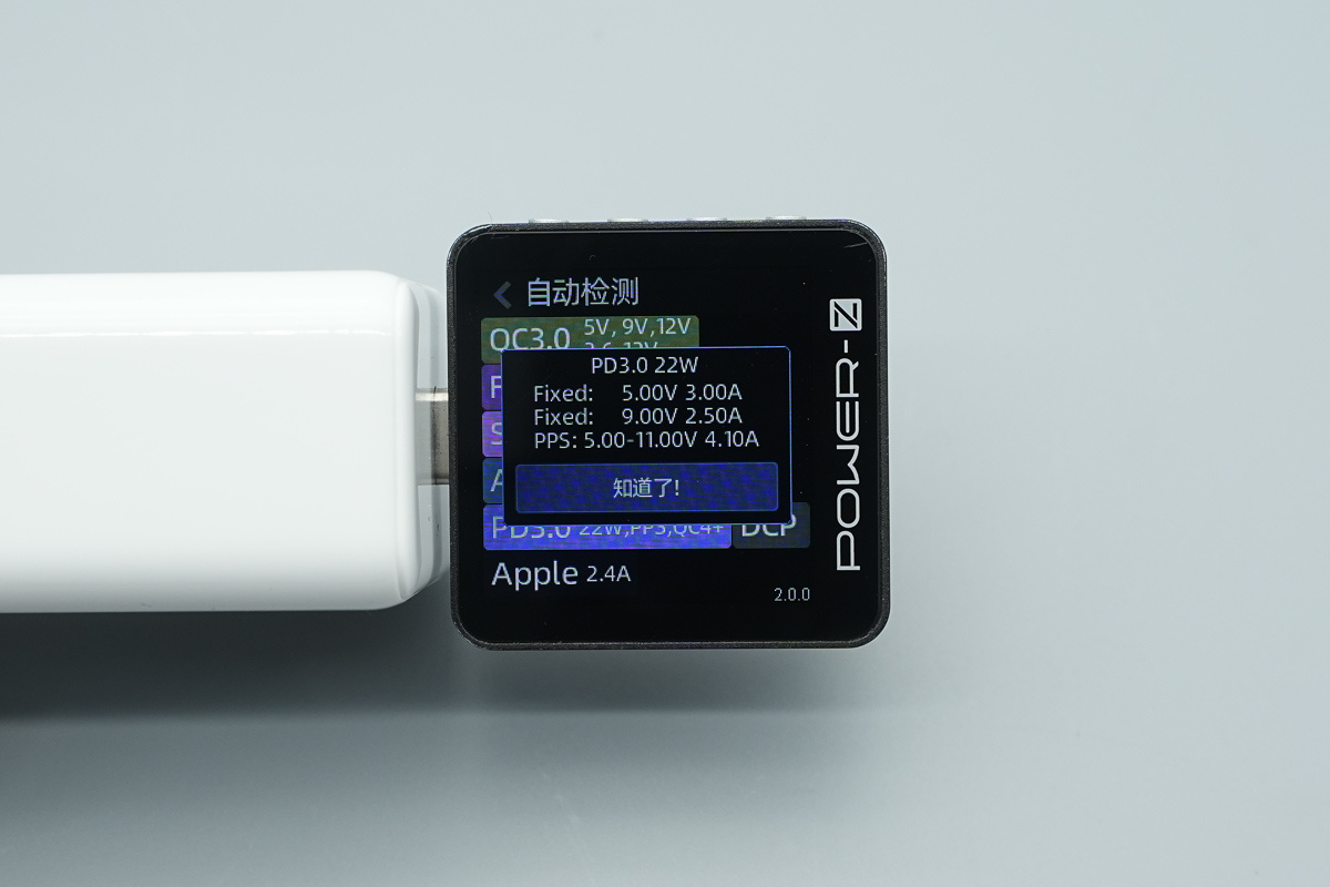
And it also supports four fixed PDOs of 5V3A, 9V2.5A, and features PPS subset: 5.00-11.00V 4.10A, maxing output of 45W.
Teardown
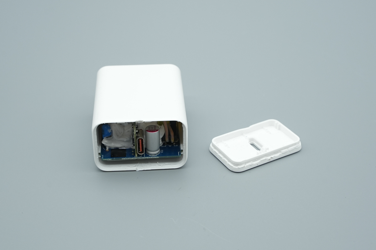
Proceeding to the teardown, the charger housing was disassembled along the casing seams, exposing the internal PCBA module.
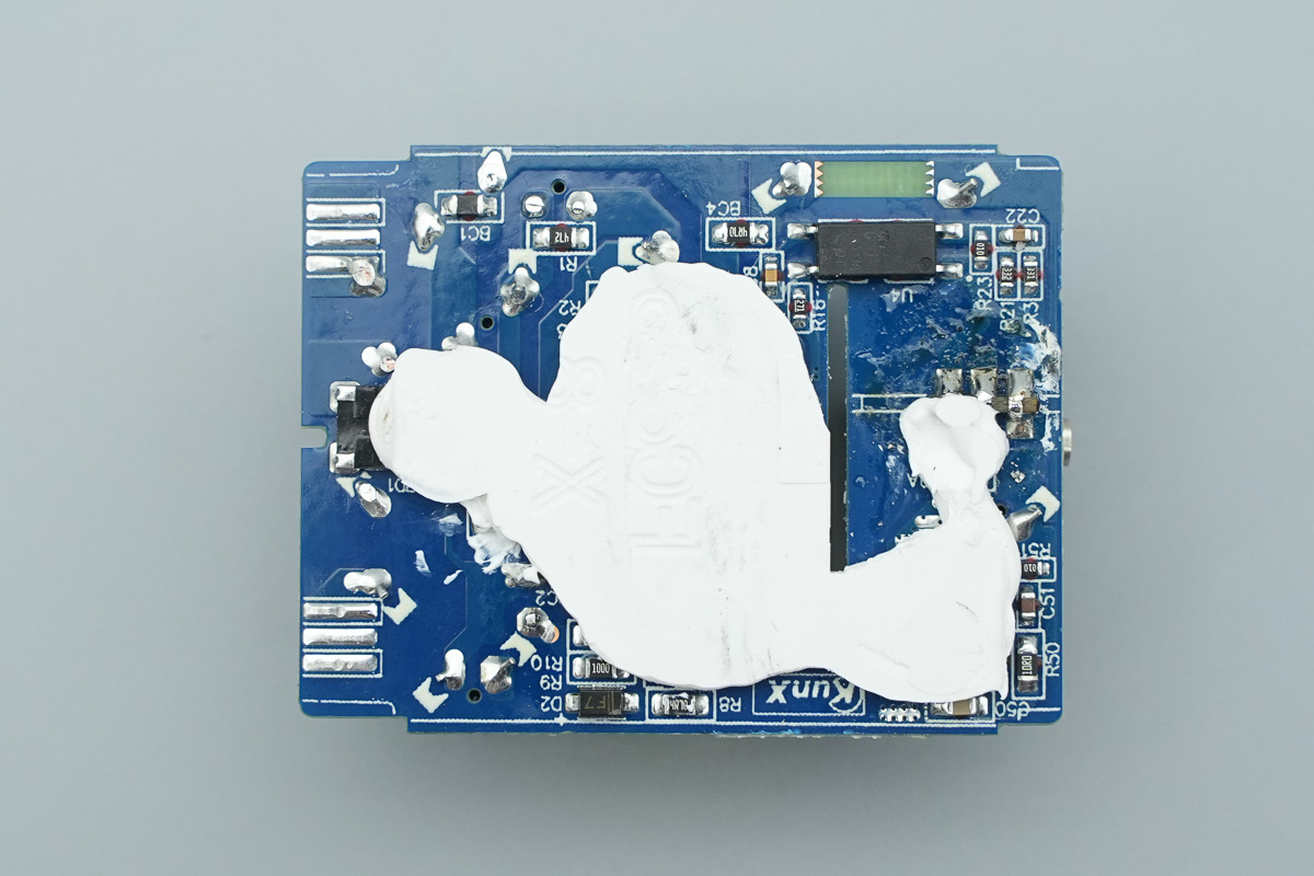
Looking through the side opening, it’s clear that the PCBA module features white thermal potting compound injected between components to achieve both structural fixation and effective heat dissipation.
Removing the PCBA module from the plastic casing.
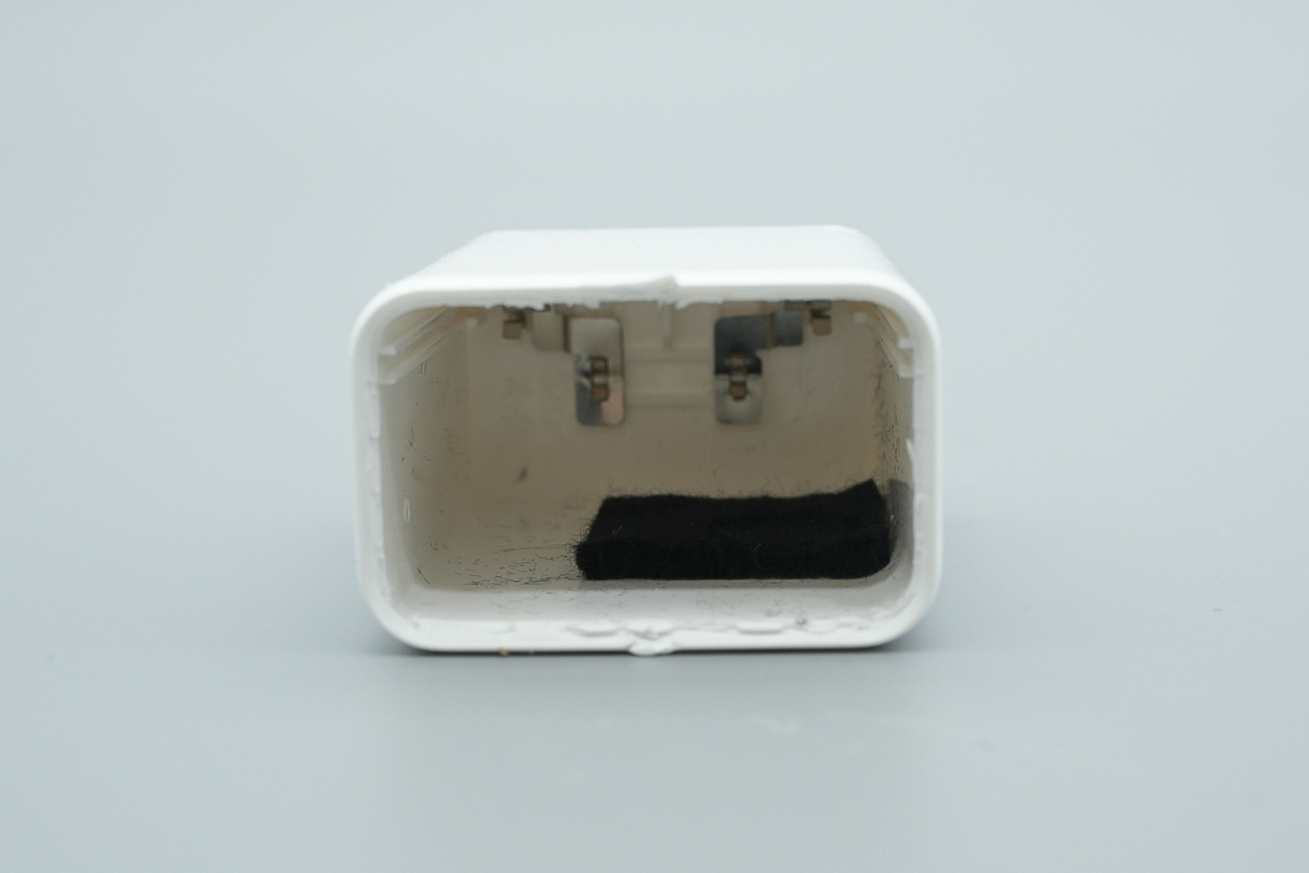
At the base of the housing, metal conductive contact plates connected to the prongs are visible, along with a piece of black cushioning isolation foam.
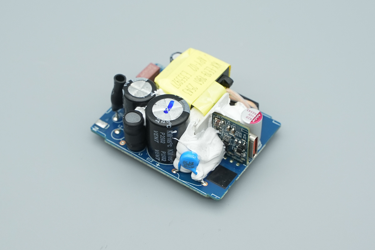
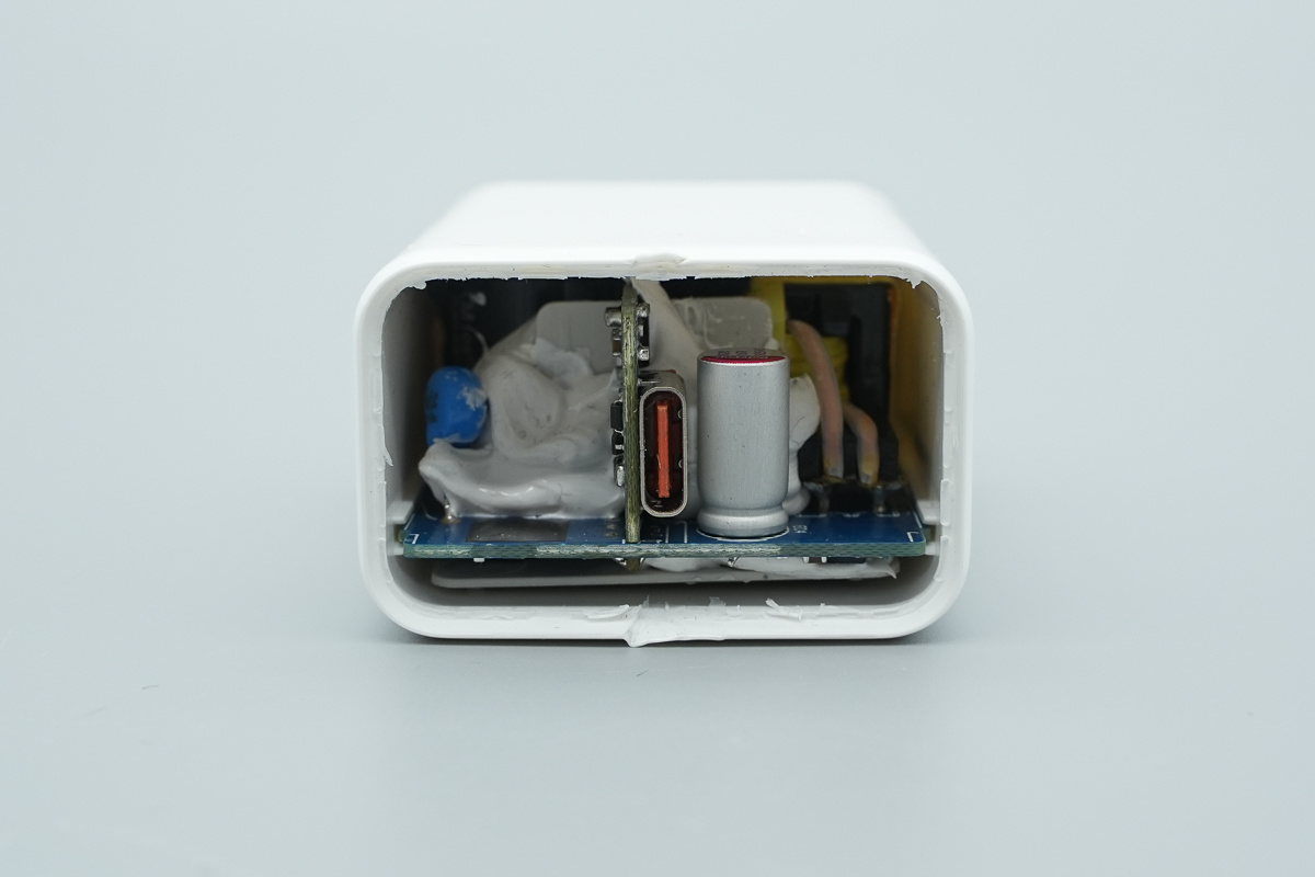
Core components such as the transformer and caps are almost entirely encapsulated in white thermal potting compound. The assembly consists of a main PCB and a output PCB.
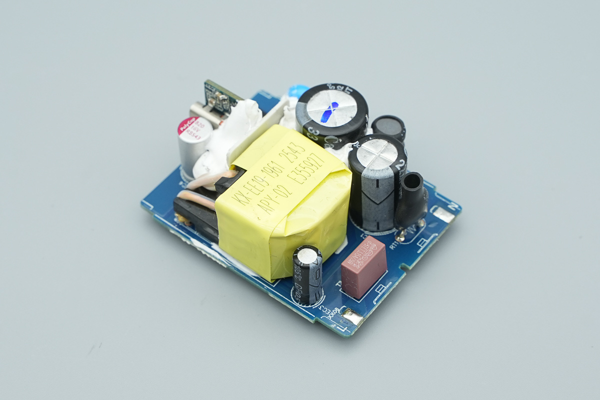
Here is a view from the opposite side.
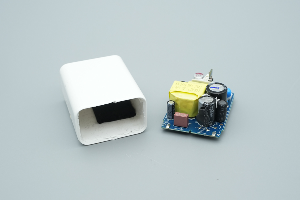
The back of the PCBA is covered by a massive brass heat sink, which is encapsulated by a white plastic insulating bracket along the edges.
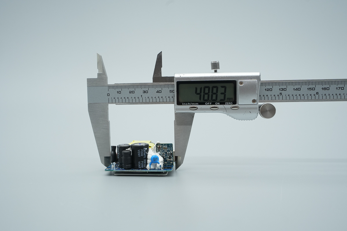
The length of PCBA is about 48.83mm (1.922 inches).
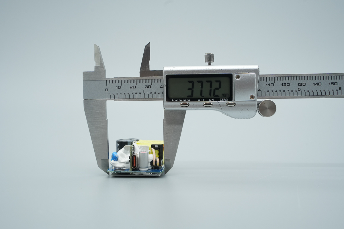
The width of PCBA is about 37.72mm (1.485 inches).
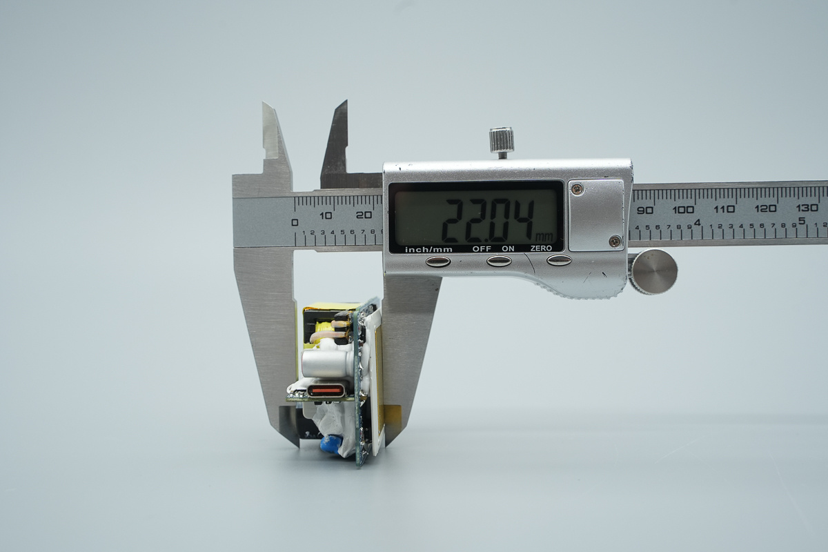
The thickness of PCBA is about 22.04mm (0.868 inches).
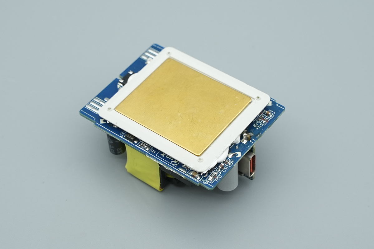
Removing the brass heat sink, we find the back of the PCB is also completely coated with white thermal potting compound.
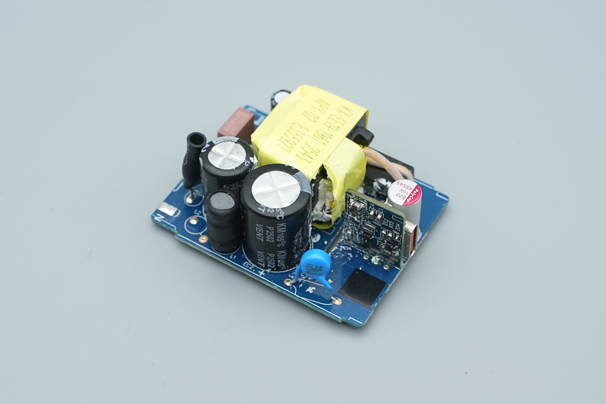
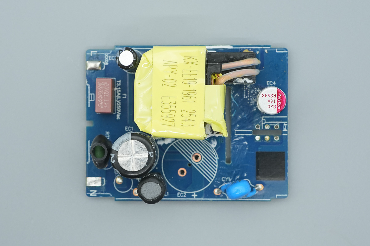
After clearing away white thermal potting compound from the front, the components on the PCBA module are clearly visible.
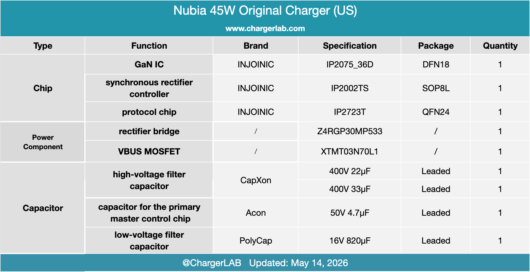
Top view of the PCBA module front: the layout reveals the input end features a time-delay fuse, an NTC thermistor, the high-voltage filter caps, the main transformer, a Y-cap, a solid cap at the output end, and the output PCB.
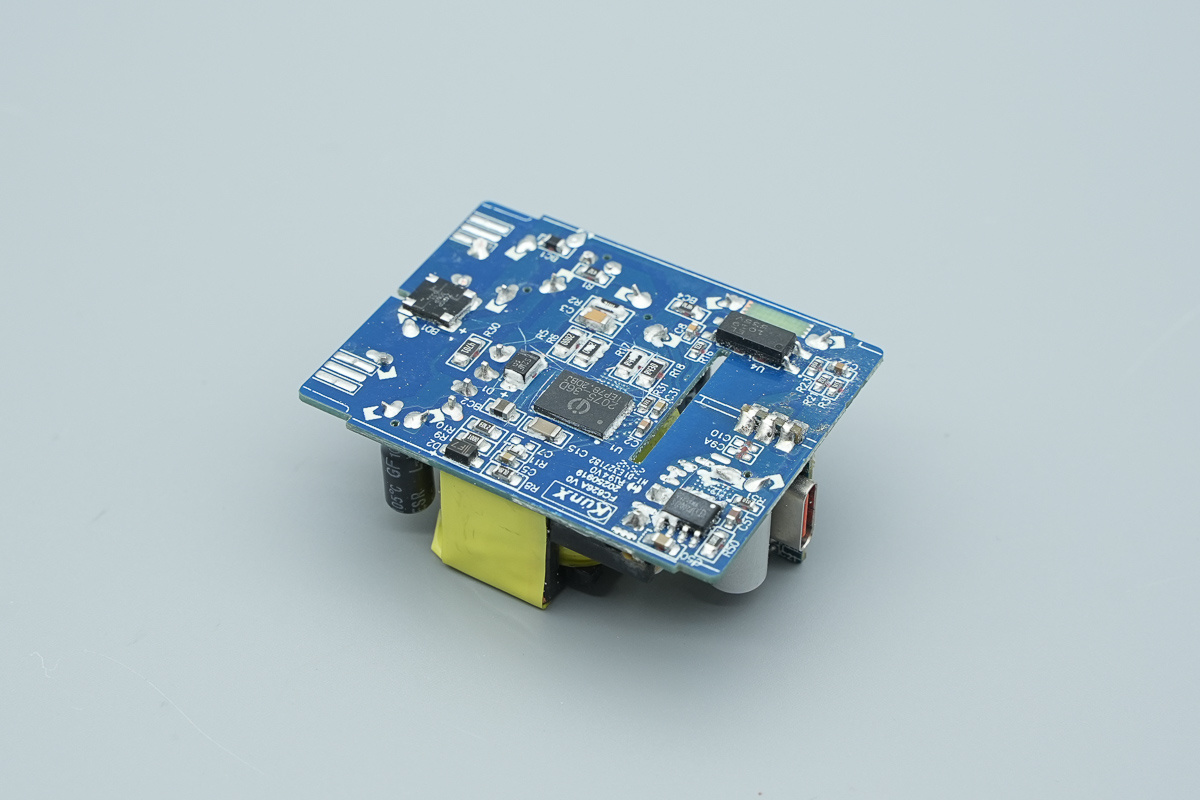
After cleaning off the white thermal potting compound, the back of the PCBA shows a distinct separation between the primary and secondary circuits.
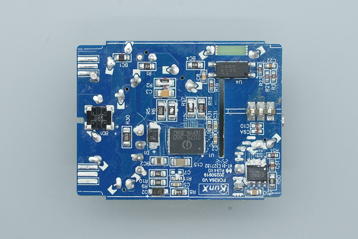
On the back of the PCBA, the core components include the SMD rectifier bridge, the primary master control chip, an optocoupler, and synchronous rectifier controller.
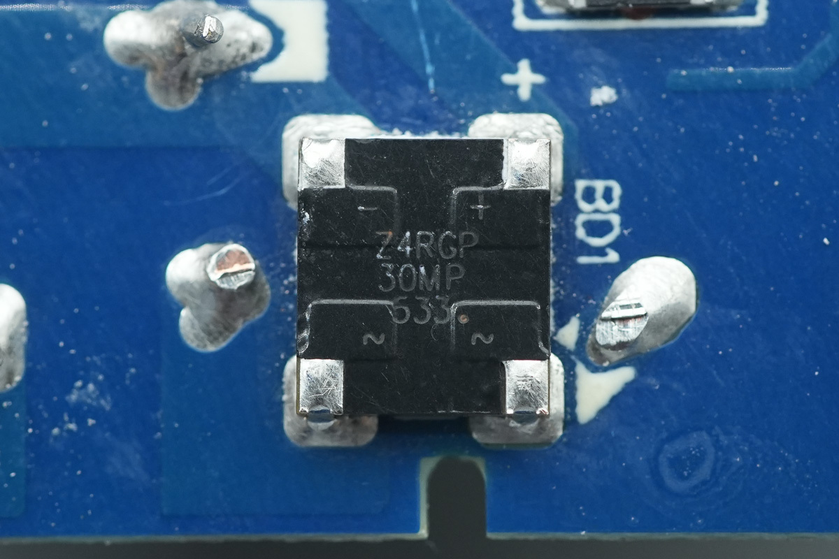
The SMD rectifier bridge at the input end, marked Z4RGP30MP533.
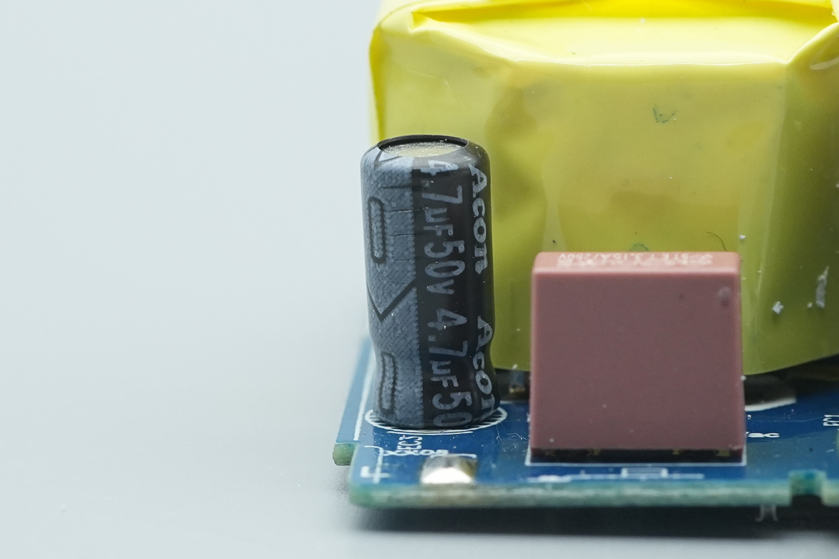
The power supply cap for the primary master control chip is from Acon, spec 50V 4.7μF.
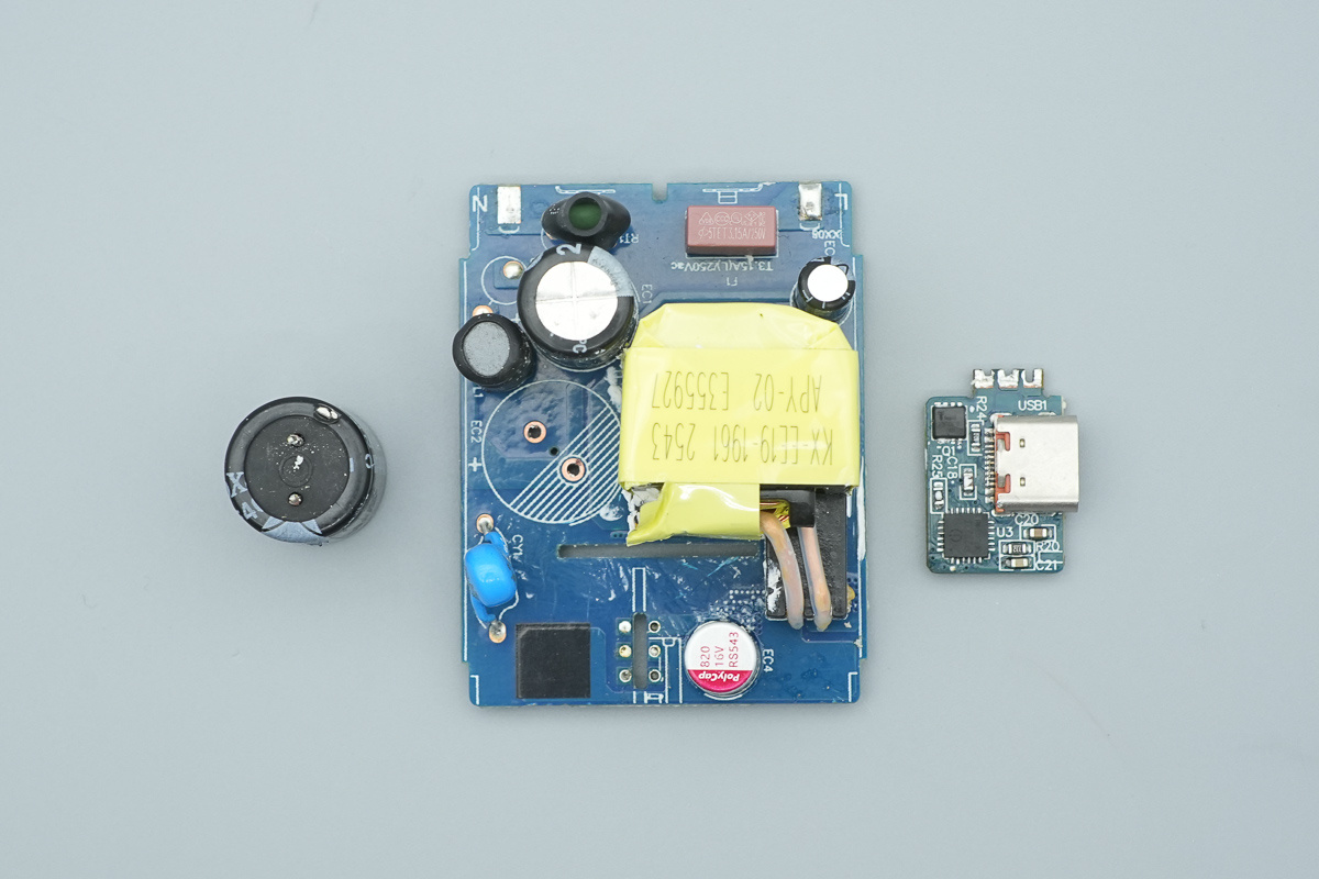
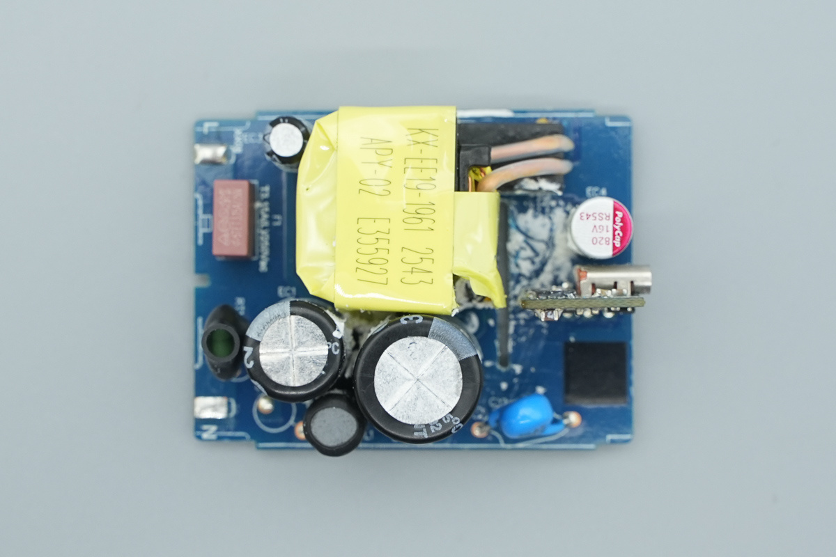
Removing the high-voltage filter caps and the USB-C output PCB.
Overview of the PCBA front after component removed.
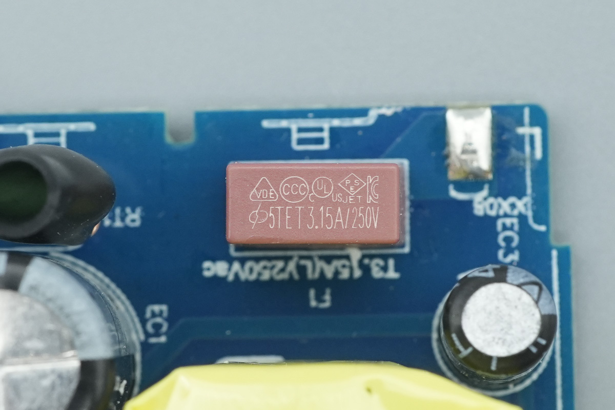
输入端的延时保险丝特写,规格为3.15A 250V。
The time-delay fuse at the input end, 3.15A 250V.
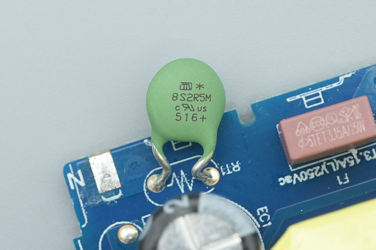
A green NTC thermistor (marked 8S2R5M) is included to curb the start-up surge as the charger connects to power.
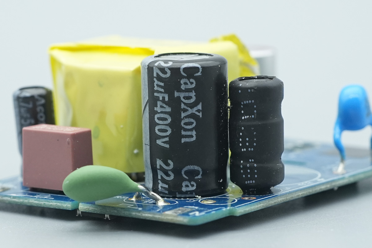
A high-voltage filter cap is from CapXon, 22μF 400V.
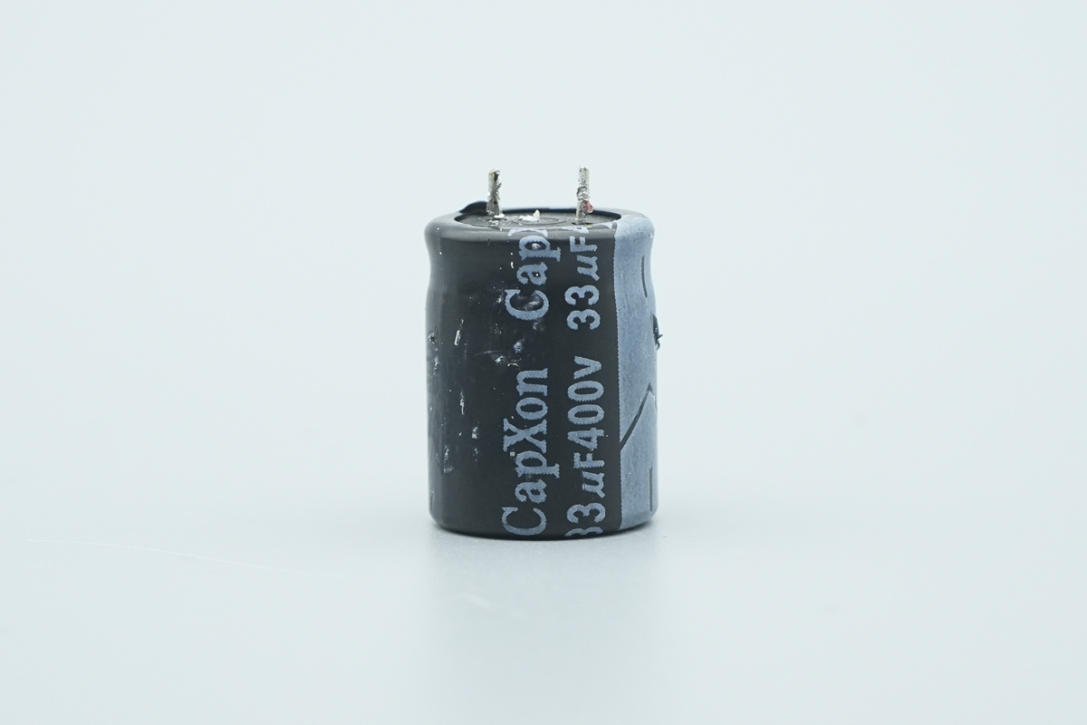
Another one is also from CapXon, spec 33μF 400V.
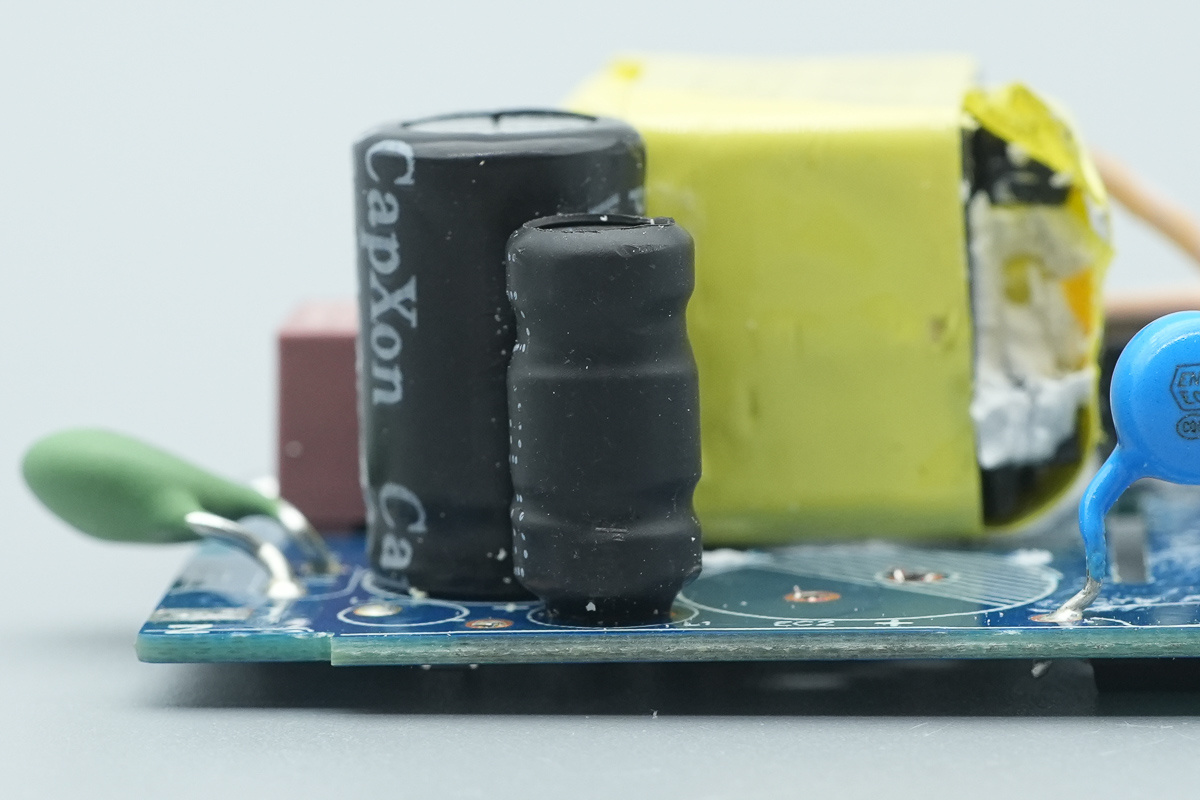
Here is an I-shaped chock wrapped in a heat-shrink tube to ensure proper insulation.
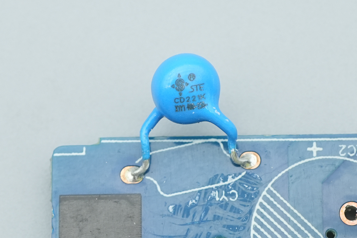
A blue Y-cap is from STE, model CD221K.
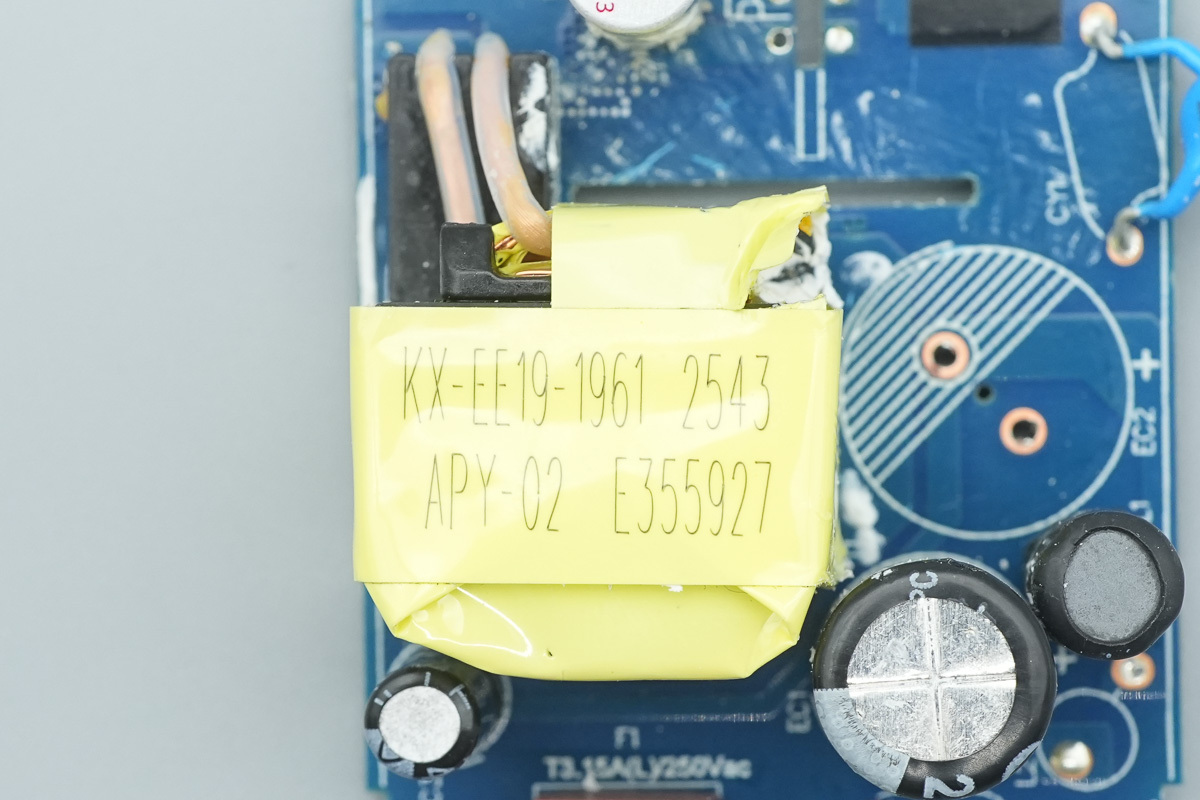
The transformer wrapped in yellow tape for insulation. The code KX-EE19-1961 2543 APY-02 E355927 is printed on the top.
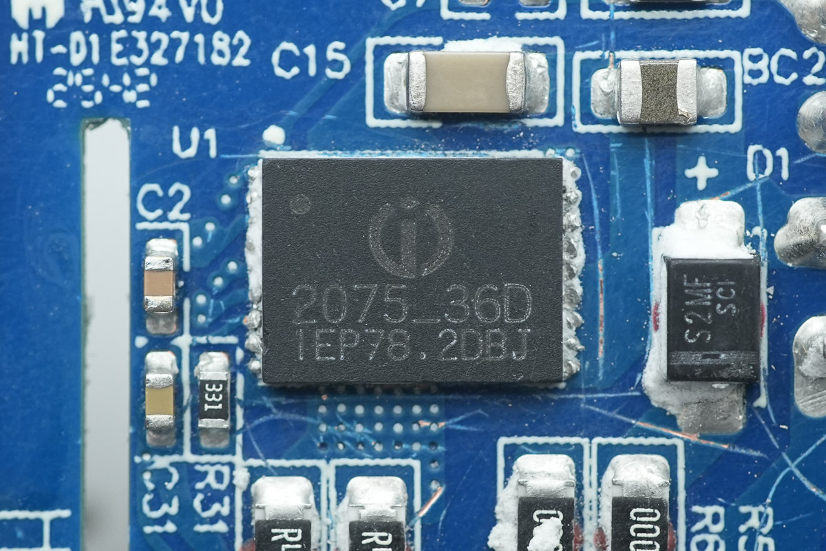
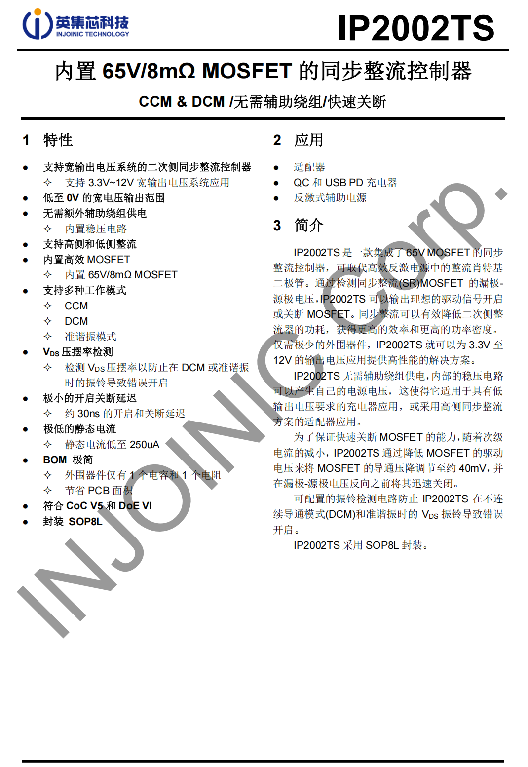
The Injoinic IP2075_36D is a high-performance, multi-mode AC/DC flyback controller featuring an integrated 700V GaN FET in a DFN18L package. It leverages adaptive control to seamlessly toggle between QR, PFM, and CCM modes via secondary-side regulation.
This high-integration GaN solution slashes the component count on the primary side, making it an ideal engine for ultra-compact, high-density PD fast chargers
It simplifies designs with a built-in high-voltage startup circuit and X-cap discharge through its HV pin, slashing standby power by ditching legacy startup resistors.
Under no-load conditions, the chip enters Burst Mode to achieve zero standby power and minimal quiescent current, easily meeting stringent Level VI energy efficiency standards such as CoC V5 and DoE VI. Furthermore, it combines frequency foldback with valley-switching technology to reduce switching losses, complemented by a built-in frequency jittering circuit to optimize EMI radiation and common-mode noise performance.
Regarding protection and packaging, the Injoinic IP2075_36D integrates a comprehensive suite of system-level protection mechanisms with extensive customizable parameters. These built-in protections include output OVP/UVP, VDD OVP, input OVP, configurable OTP, and OPP with compensation.
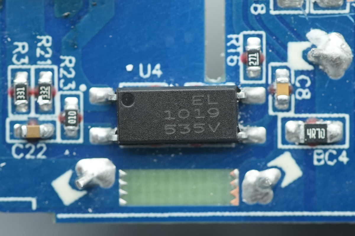
An optocoupler, marked EL1019.
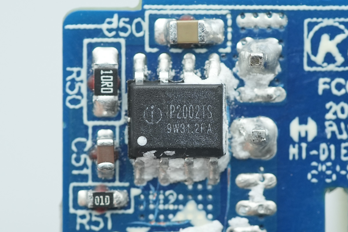
The synchronous rectifier controller is from Injoinic, model IP2002TS, with an integrated 65V MOSFET, designed to replace Schottky rectifier diodes in high-efficiency flyback power supplies.
By sensing the drain-to-source voltage of the SR MOSFET, it generates an ideal drive signal to toggle the MOSFET. This implementation effectively slashes power loss in secondary-side rectifiers, enabling superior efficiency and higher power density.
It provides a high-performance solution for output voltage applications ranging from 3.3V to 12V with minimal peripheral components. It eliminates the need for an auxiliary winding power supply, as the internal regulator circuit generates its own supply voltage. This makes it ideal for chargers with low output voltage requirements or adapters utilizing high-side SR schemes.
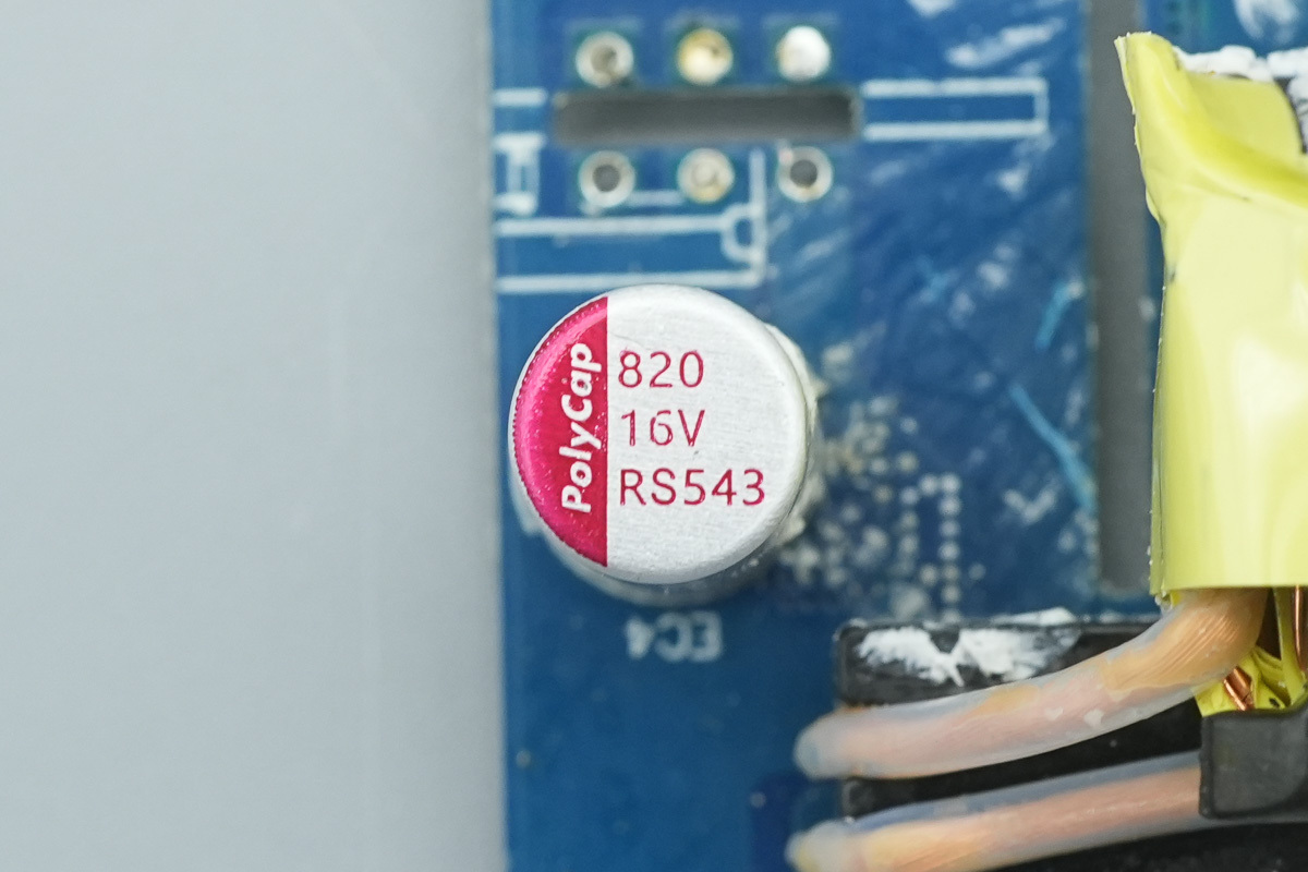
The output-side filter solid cap is from PolyCap, 820μF 16V.
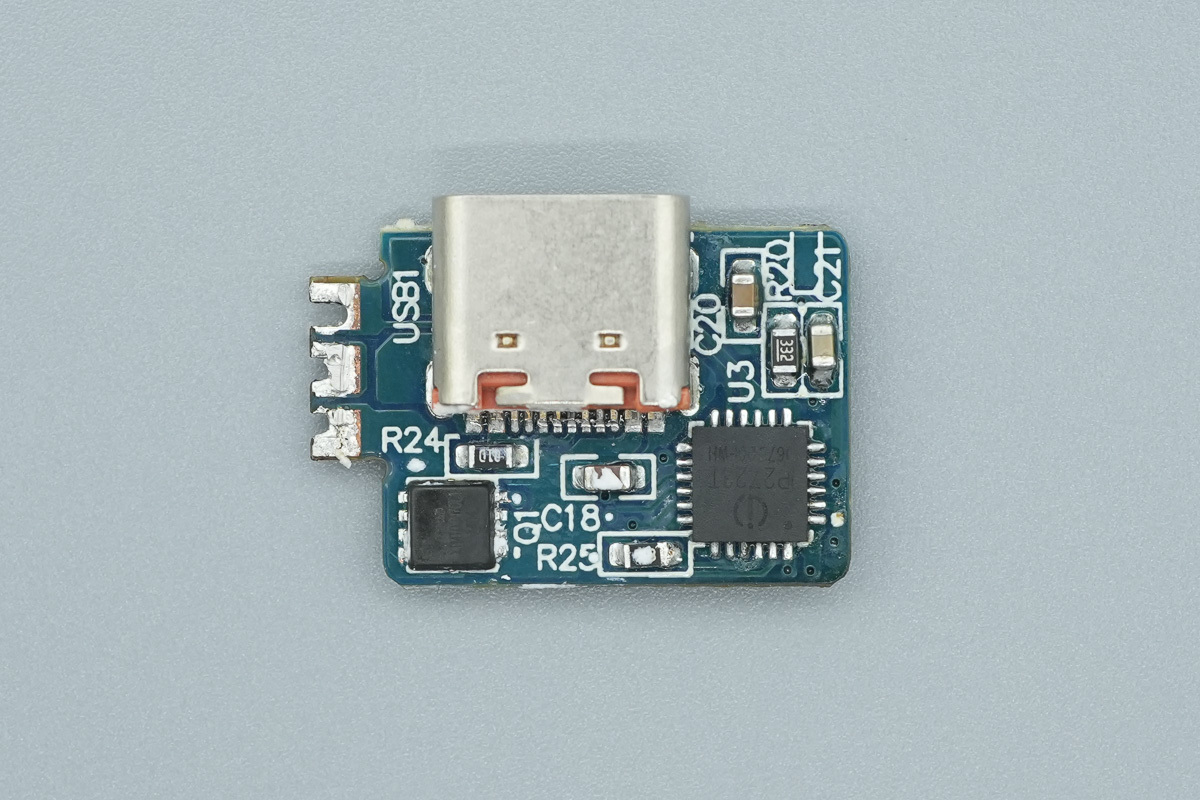
Overview of the USB-C output protocol PCB front, featuring the USB-C sockets, the protocol chip, and the VBUS MOSFET.
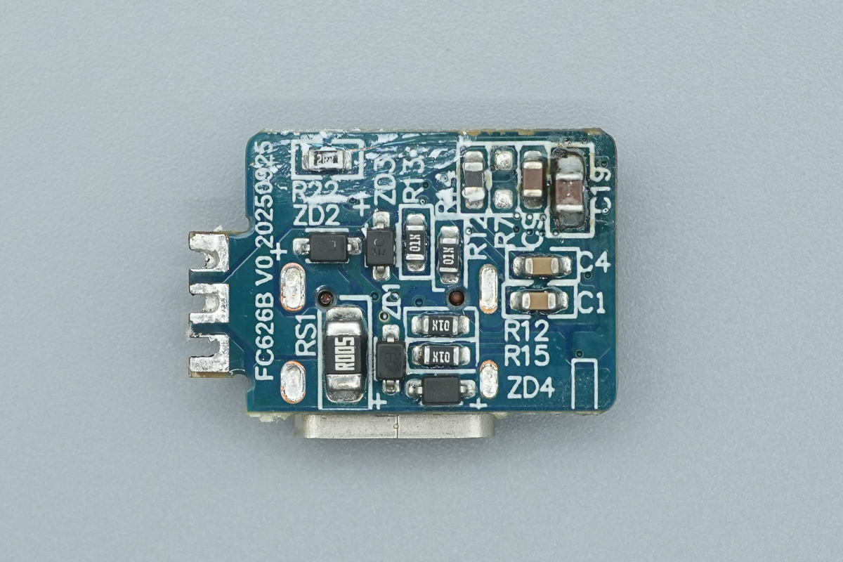
A view of the back of the USB-C output protocol PCB.
The plastic sheet inside the USB-C sockets is red.
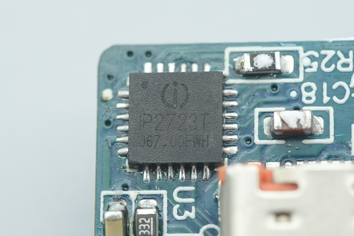
The protocol chip is also from Injoinic, model IP2723T. This MTP-based fast charging protocol IC integrates multiple standards for USB output ports, allowing for customizable power allocation and expanded functionalities based on client requirements. It delivers a comprehensive Type-C solution for unidirectional output applications such as power adapters and car chargers.
Highly integrated and feature-rich, it requires minimal peripheral components, effectively shrinking the overall solution size and reducing BOM.
It supports USB PD2.0/PD3.0/PPS, HVDCP QC4/QC4+/QC3.0/QC2.0, Huawei FCP/SCP, Samsung AFC, MTK PE+ 2.0/1.1, Apple 2.4A and BC1.2, in QFN24 package.
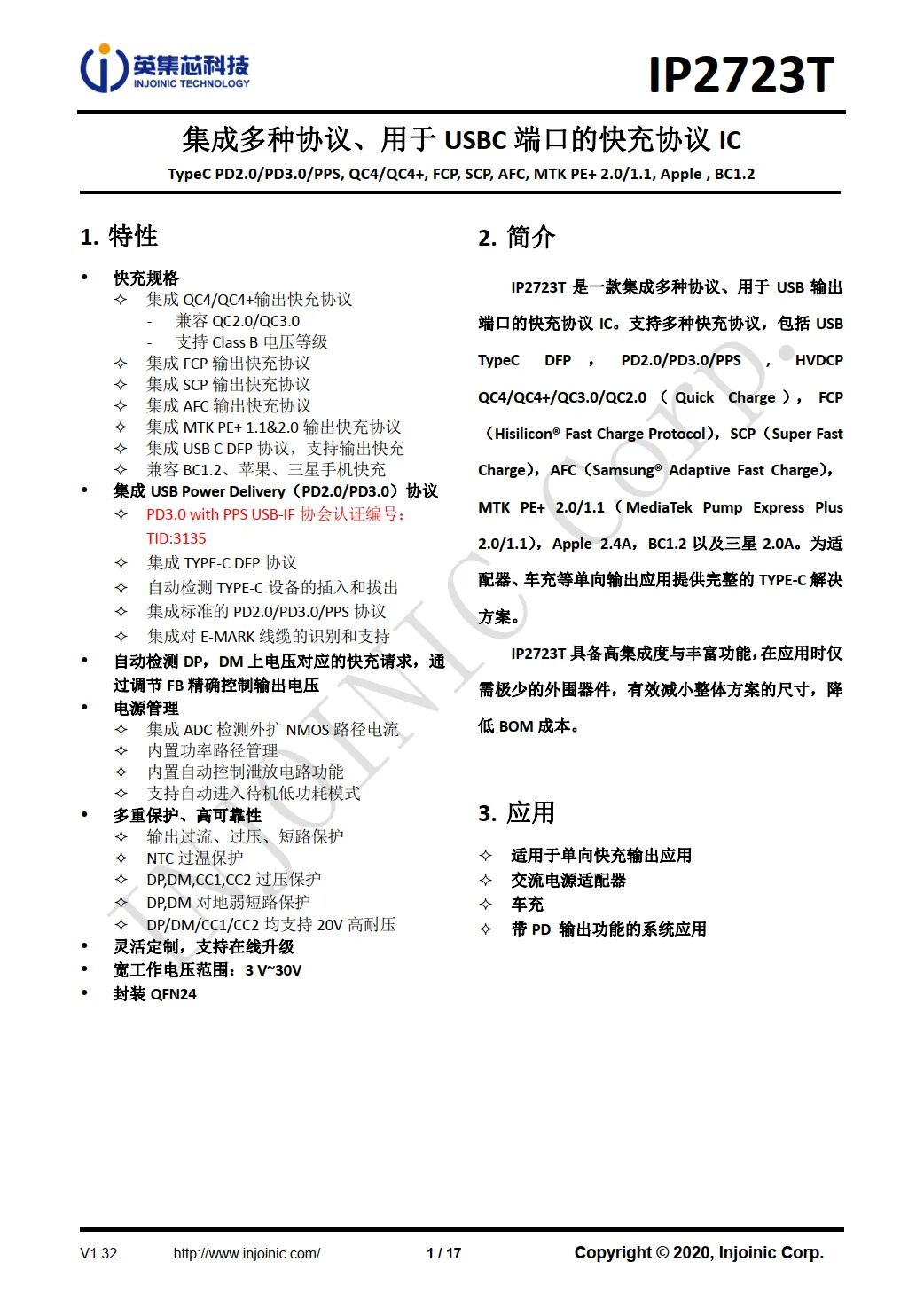
This VBUS MOSFET is marked with XTMT03N70L1.
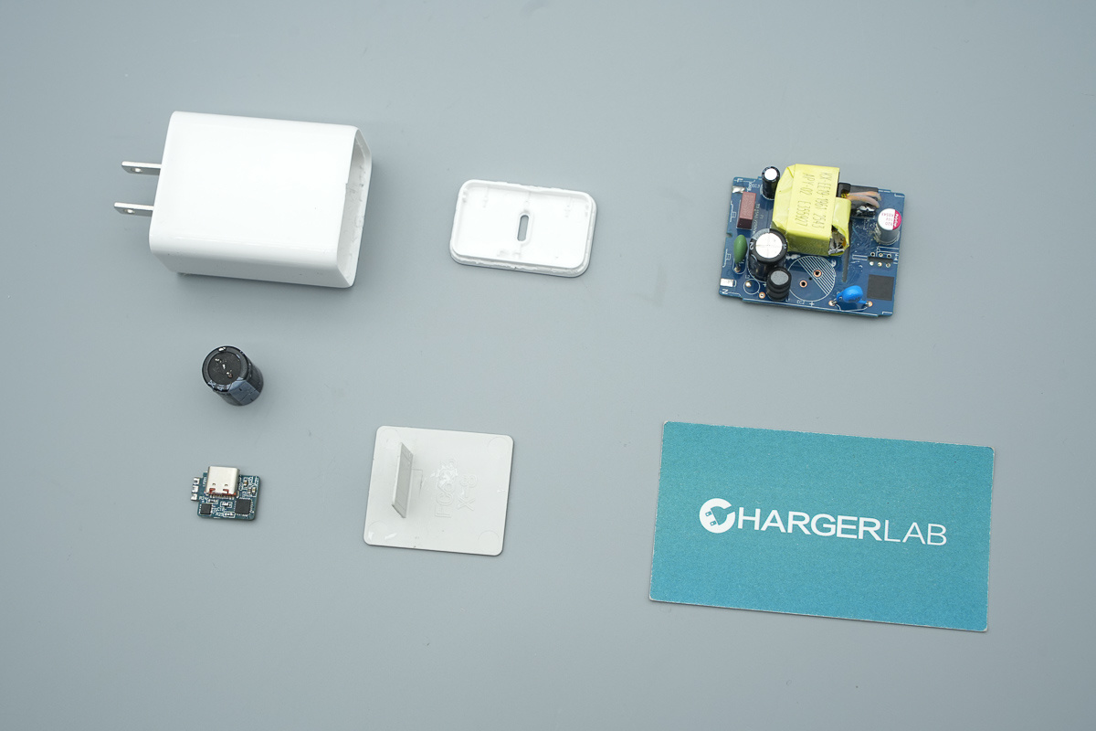
Well, those are all components of The Nubia 45W original charger.
Summary of ChargerLAB
The Nubia 45W single USB-C charger features a sleek, high-gloss white shell paired with a fixed US-standard plug, achieving a highly compact and portable form factor. The port is designed with the brand's signature red plastic sheet. Testing confirms support for a wide range of protocols, including QC, FCP, SCP, PD3.0, and PPS, meeting the fast-charging needs of most modern smartphones and tablets.
Built with using ultrasonic welding. Inside, the PCBA module is heavily potted with white thermal potting compound and equipped with a large brass heatsink and plastic insulation bracket on the rear. This design significantly enhances the heat dissipation of core components under full-load conditions while ensuring structural stability and insulation.
For the core components, it utilizes a full suite of Injoinic fast-charging solutions, including the IP2075_36D primary master control chip, IP2002TS secondary synchronous rectifier controller, and IP2723T protocol chip. This allows for an exceptionally high level of integration and streamlined peripheral circuitry.
Furthermore, CapXon caps are selected for high-voltage filtering, while PolyCap solid caps are used for output-side filtering. Overall, this charger exhibits solid craftsmanship and reliable material selection, making it an excellent original-grade product.
Related Articles:
1. Unboxing of Nubia Candy Power Bank S1
2. Unboxing of Nubia RedMagic DAO 45W Mini GaN Charger
3. Unboxing of Nubia RedMagic DAO 35W Mini GaN Charger