Introduction
Xiaomi has released a new 67W GaN charger featuring three ports, including two USB-C and one USB-A. All three ports support 65W PD and 67W Surge Turbo Charging. The charger also offers a 45W + 20W dual-port fast-charging configuration. It comes with a 6A cable to ensure a reliable user experience without the need for an additional purchase. The following provides a closer look at this product.
Product Appearance
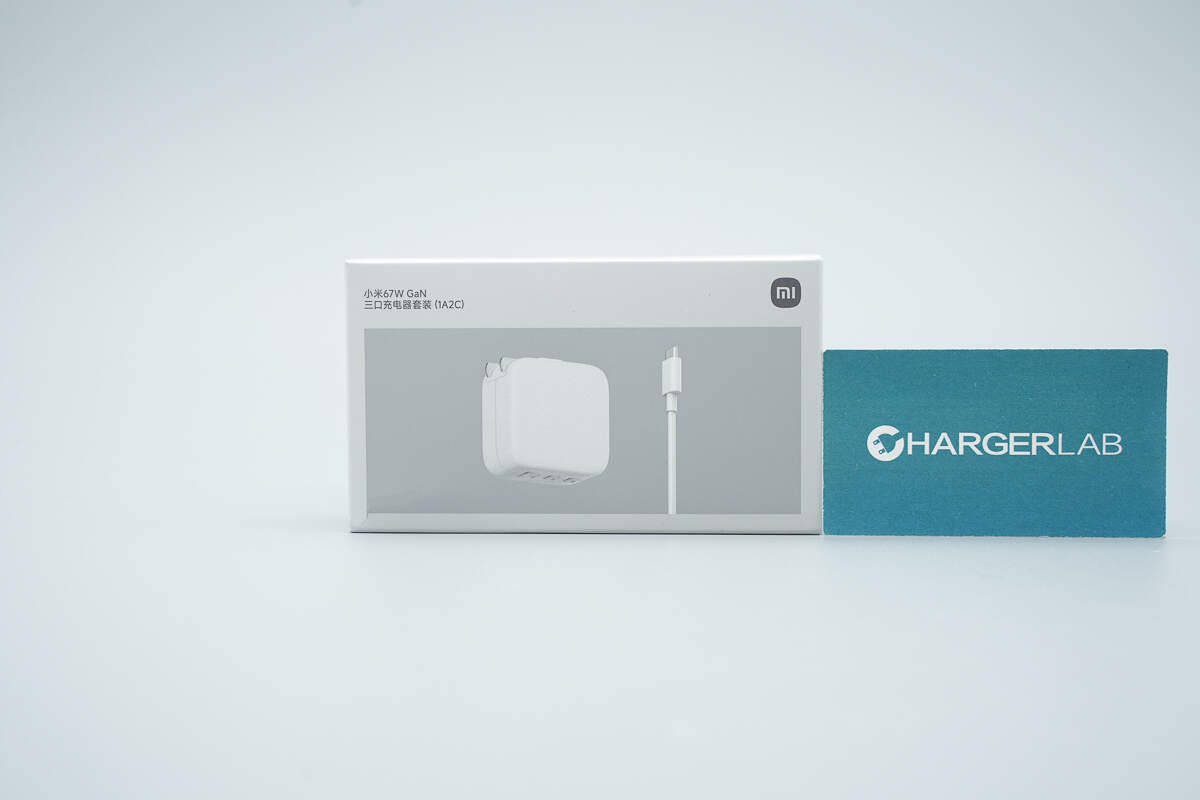
The front of the packaging features the Xiaomi logo along with an image of the product.
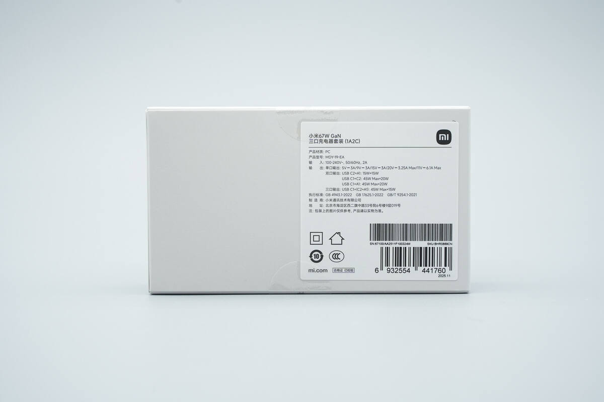
A specification label is affixed to the back of the packaging.
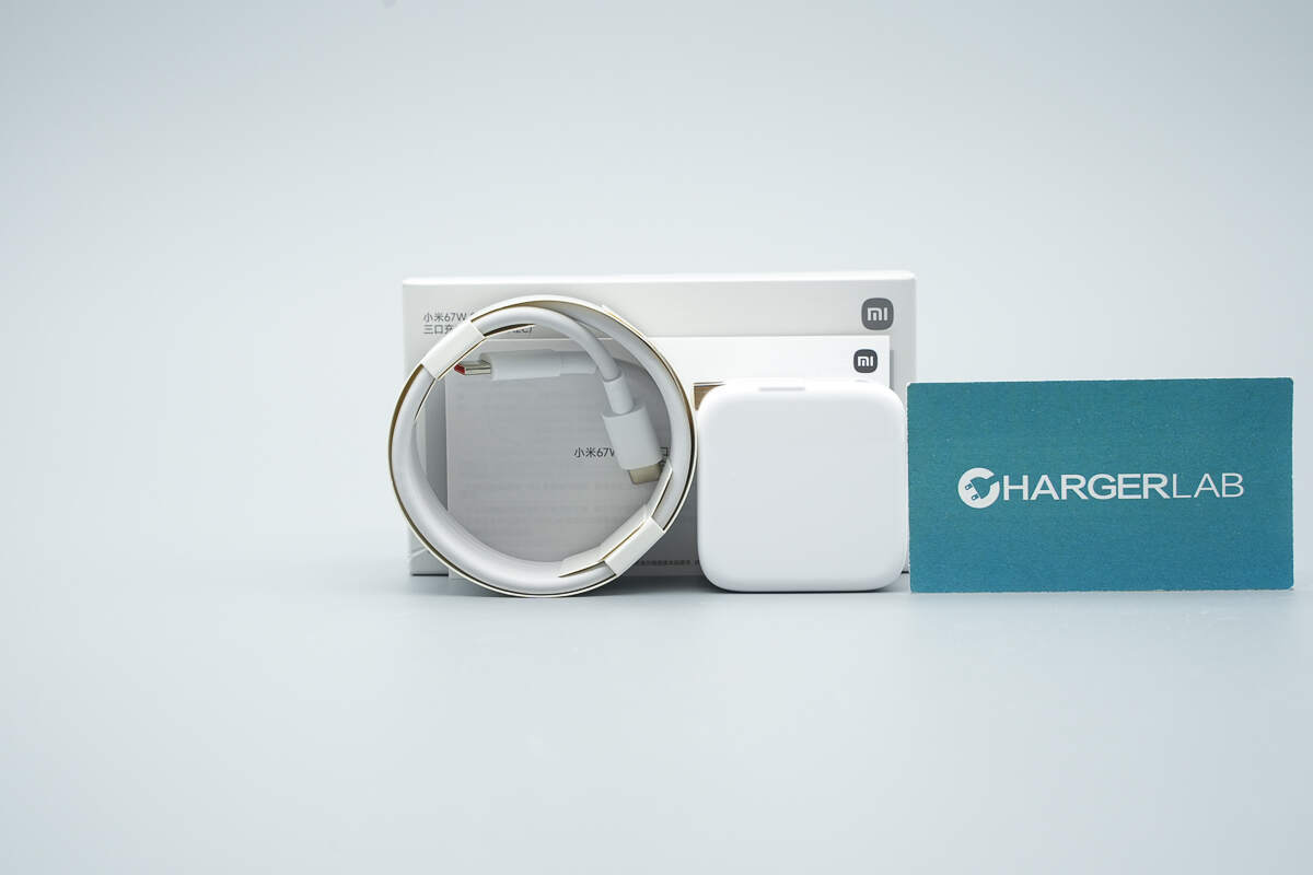
The package includes the charger, a data cable, and a user manual.
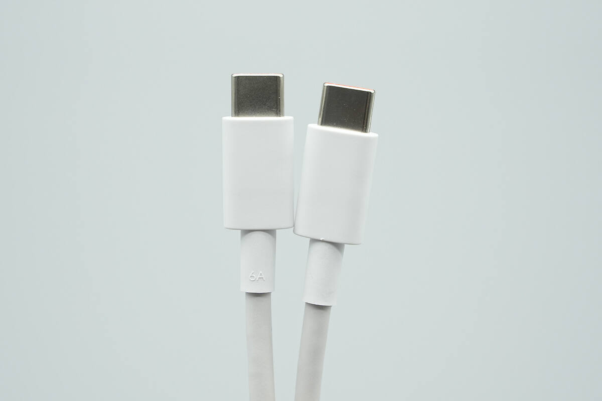
The included cable is rated for 6A.
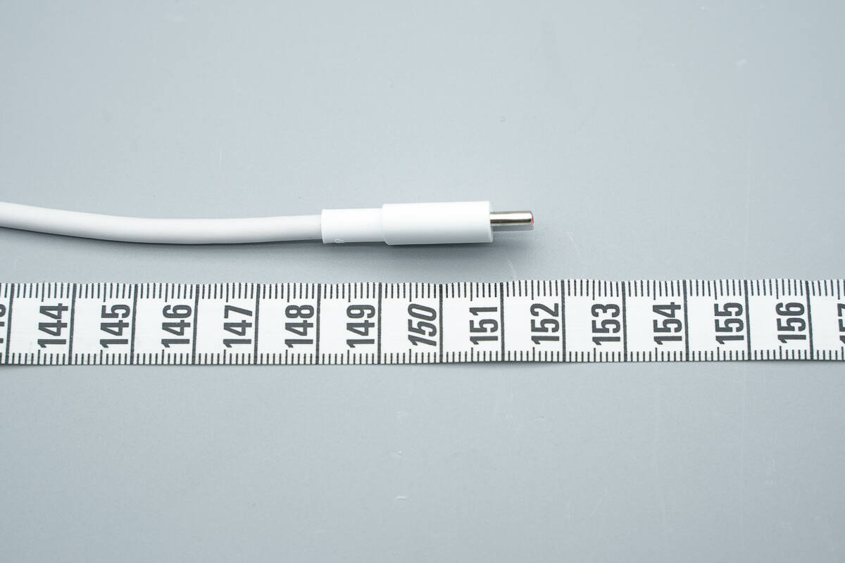
The length of the cable is about 151.5 cm (59.65 inches).
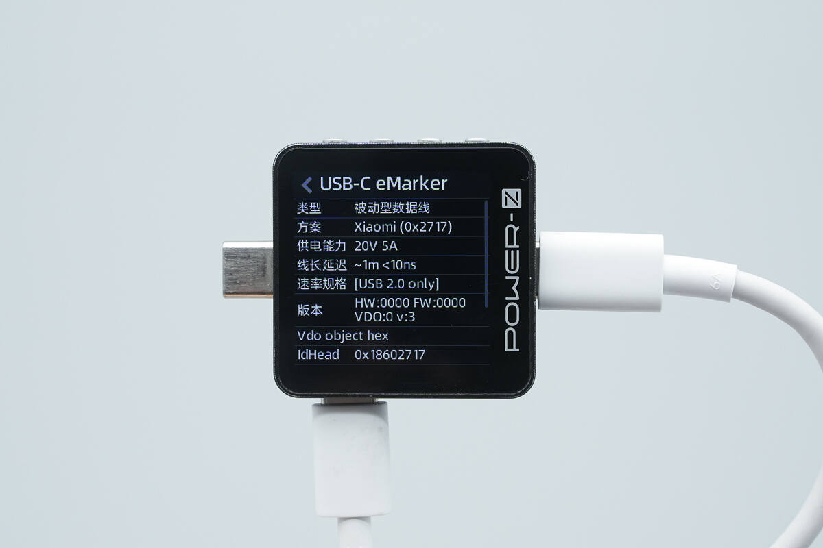
ChargerLAB POWER-Z KM003C shows it has an E-Marker chip. Its power transmission capability is 20V5A, and its data transmission capability is USB 2.0.
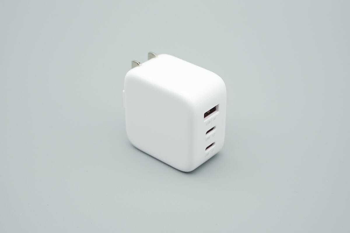
The exterior features a high-gloss finish with smoothly rounded edges.

The input side is equipped with foldable prongs and printed specifications.
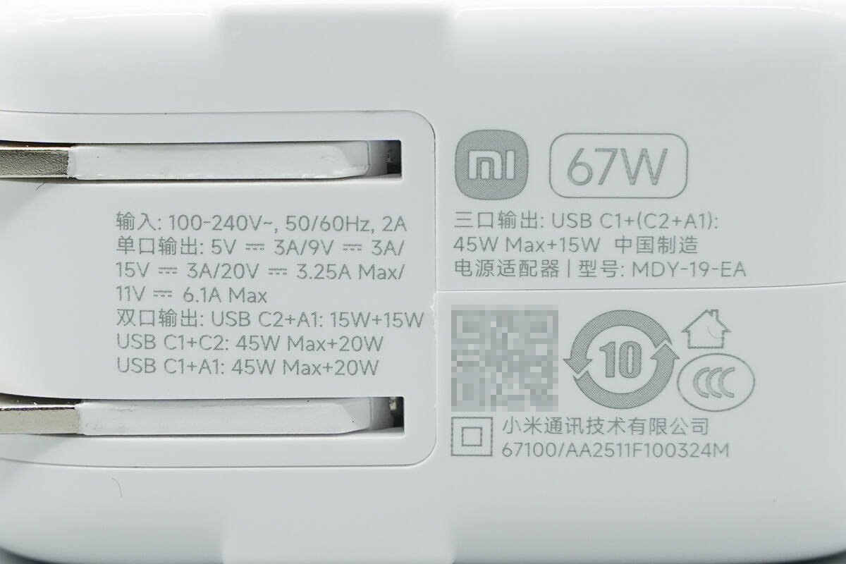
Model: MDY-19-EA
Input: 100–240V~ 50/60Hz 2A
Single-port output: 5V 3A, 9V 3A, 15V 3A, 20V 3.25A Max, 11V 6.1A Max
Dual-port output:
USB-C2 + A1: 15W + 15W
USB-C1 + C2: 45W Max + 20W
USB-C1 + A1: 45W Max + 20W
Triple-port output: USB-C1 + (C2 + A1): 45W Max + 15W
The product is CCC certified.
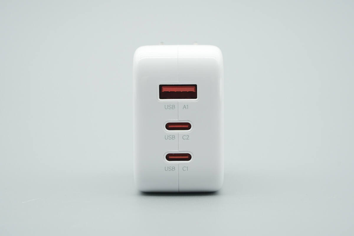
The output side is equipped with two USB-C ports and one USB-A port, each labeled with the corresponding markings.
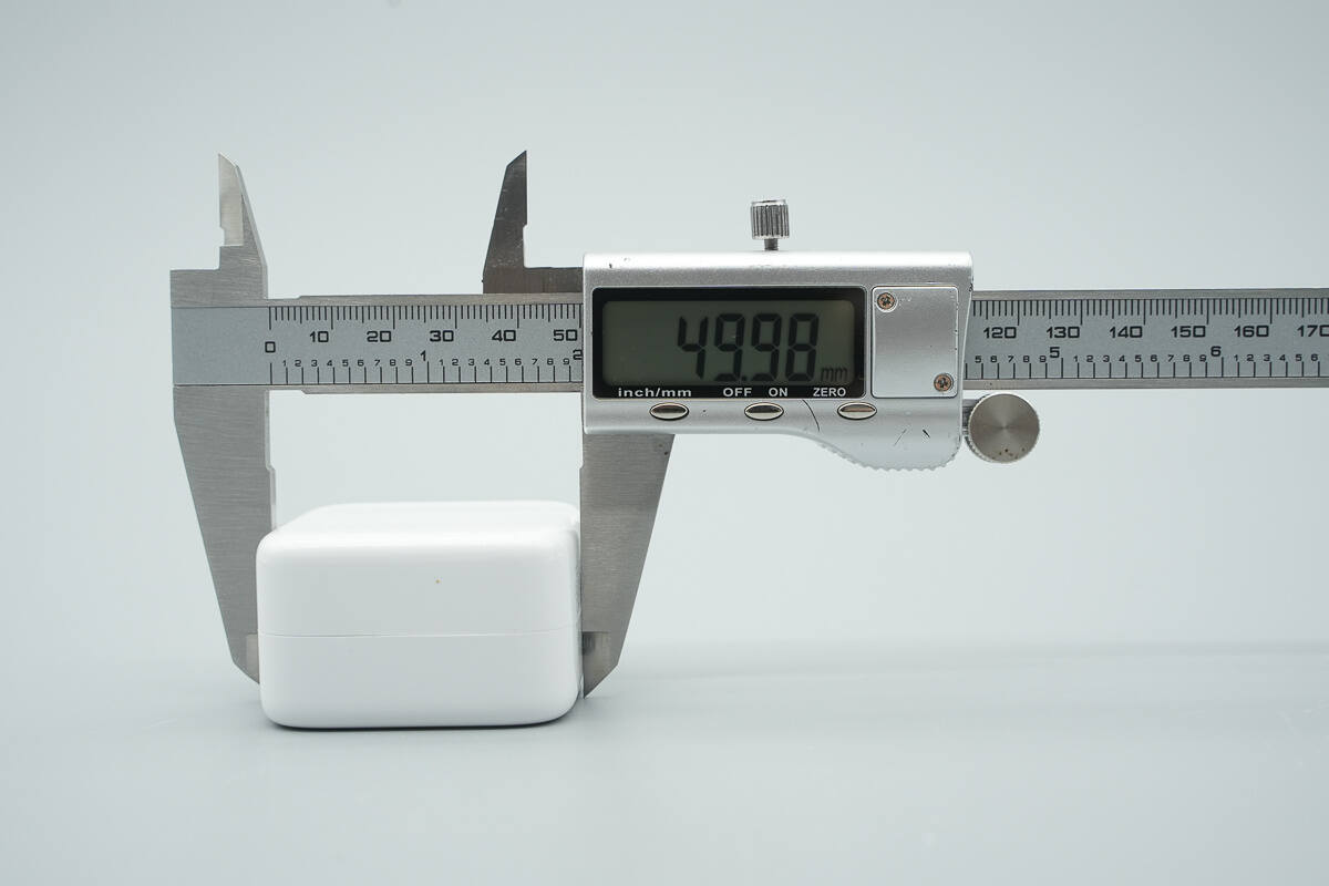
The length of the charger is about 49.98 mm (1.97 inches).
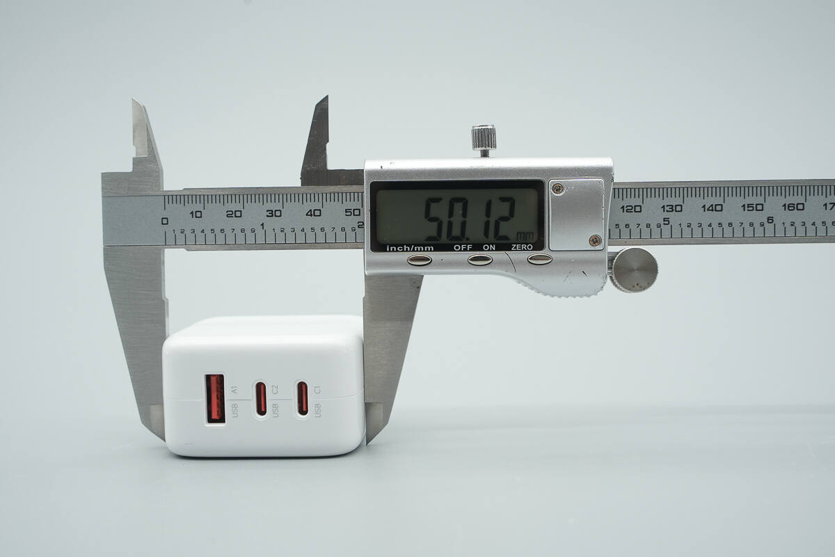
The width is about 50.12 mm (1.97 inches).
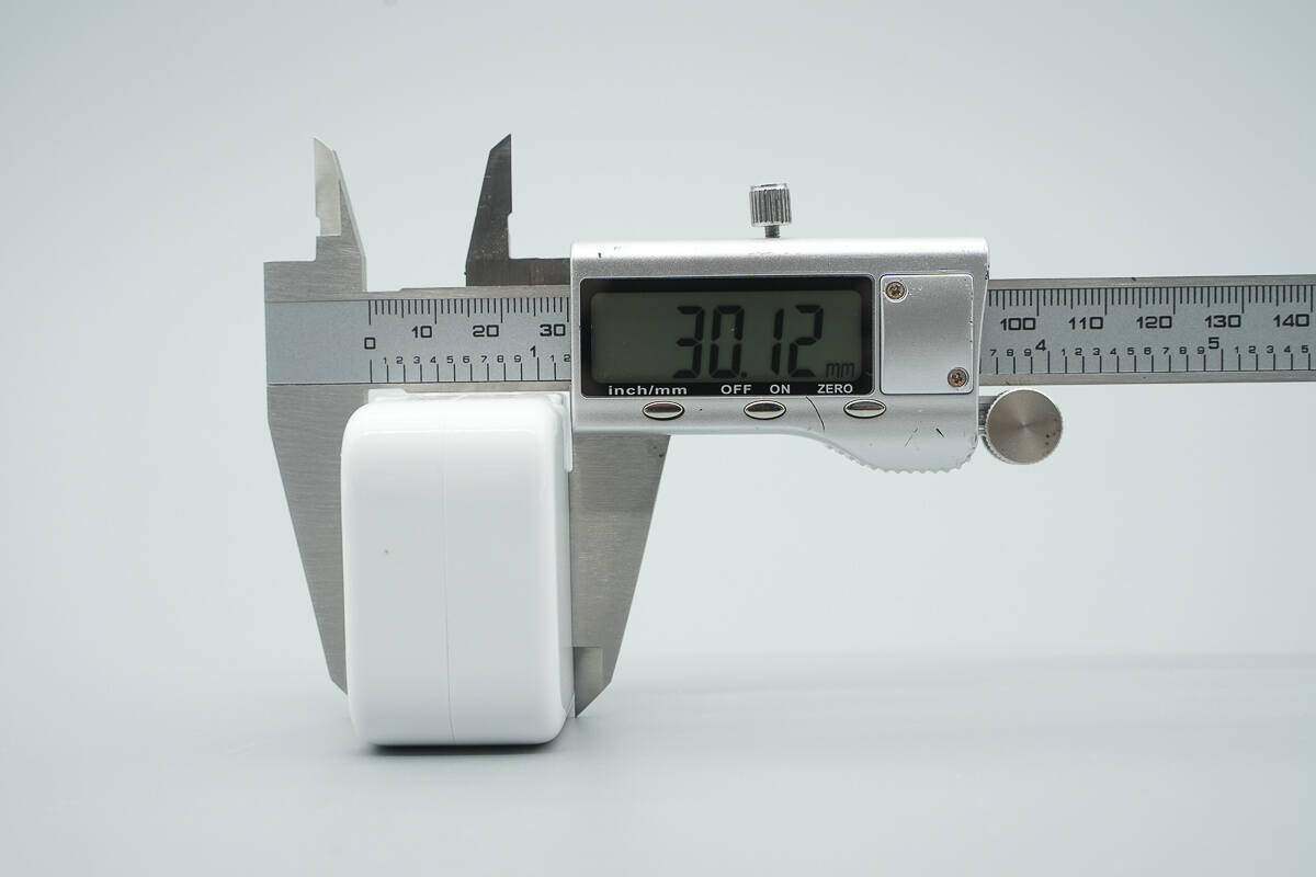
The thickness is about 30.12 mm (1.19 inches).
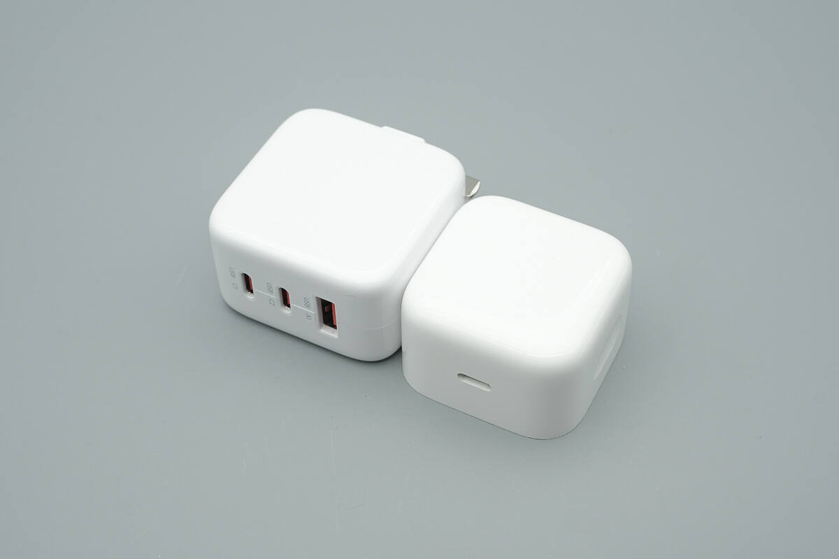
Compared side by side with the Apple 40W Dynamic Charger, the Xiaomi unit is only slightly larger.
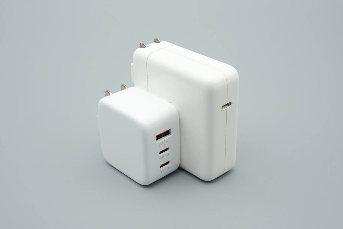
Compared with the Apple 67W charger, its size advantage is obvious.

That's how big it is on the hand.
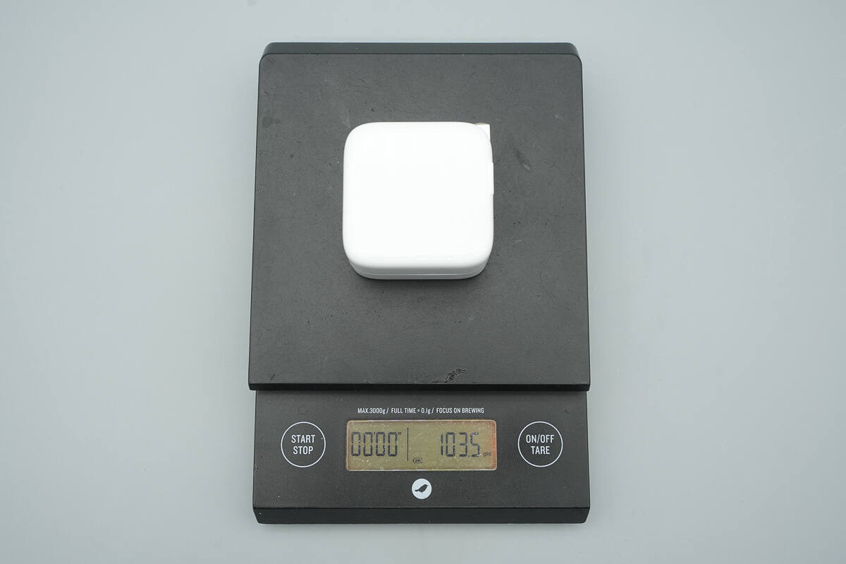
The weight is about 104 g (3.67 oz).
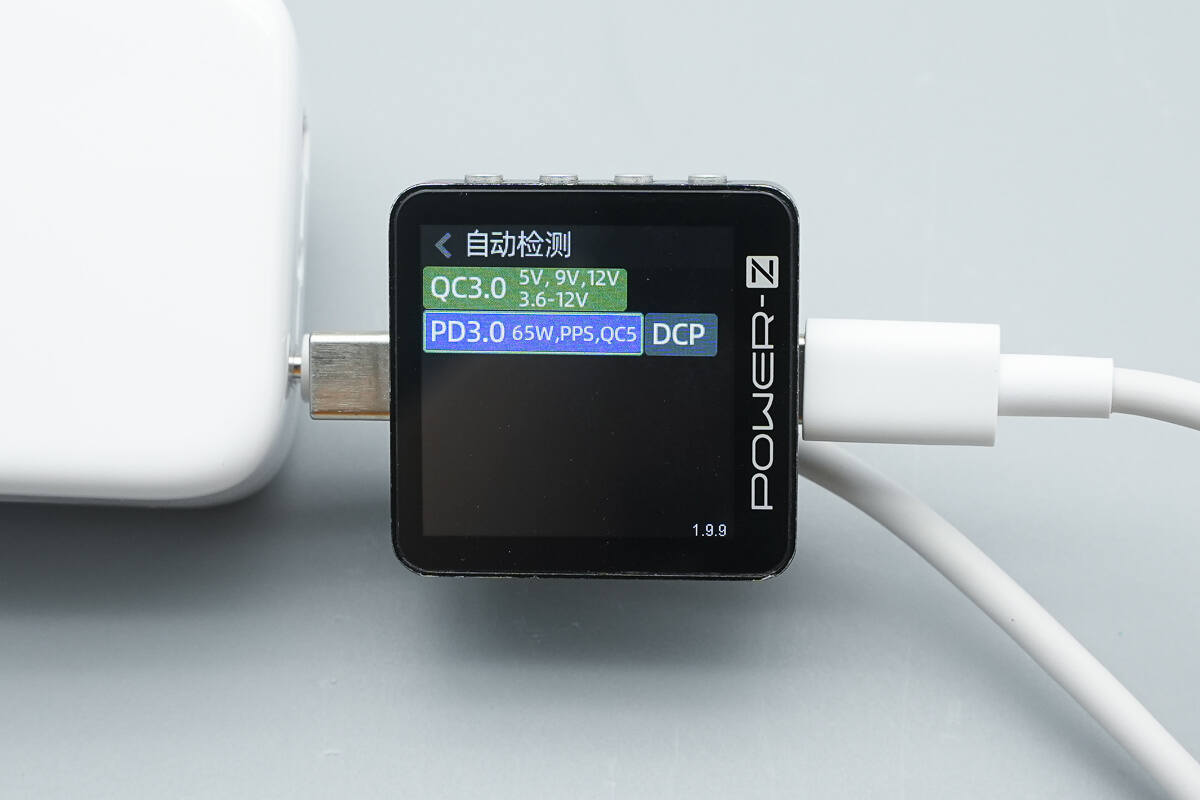
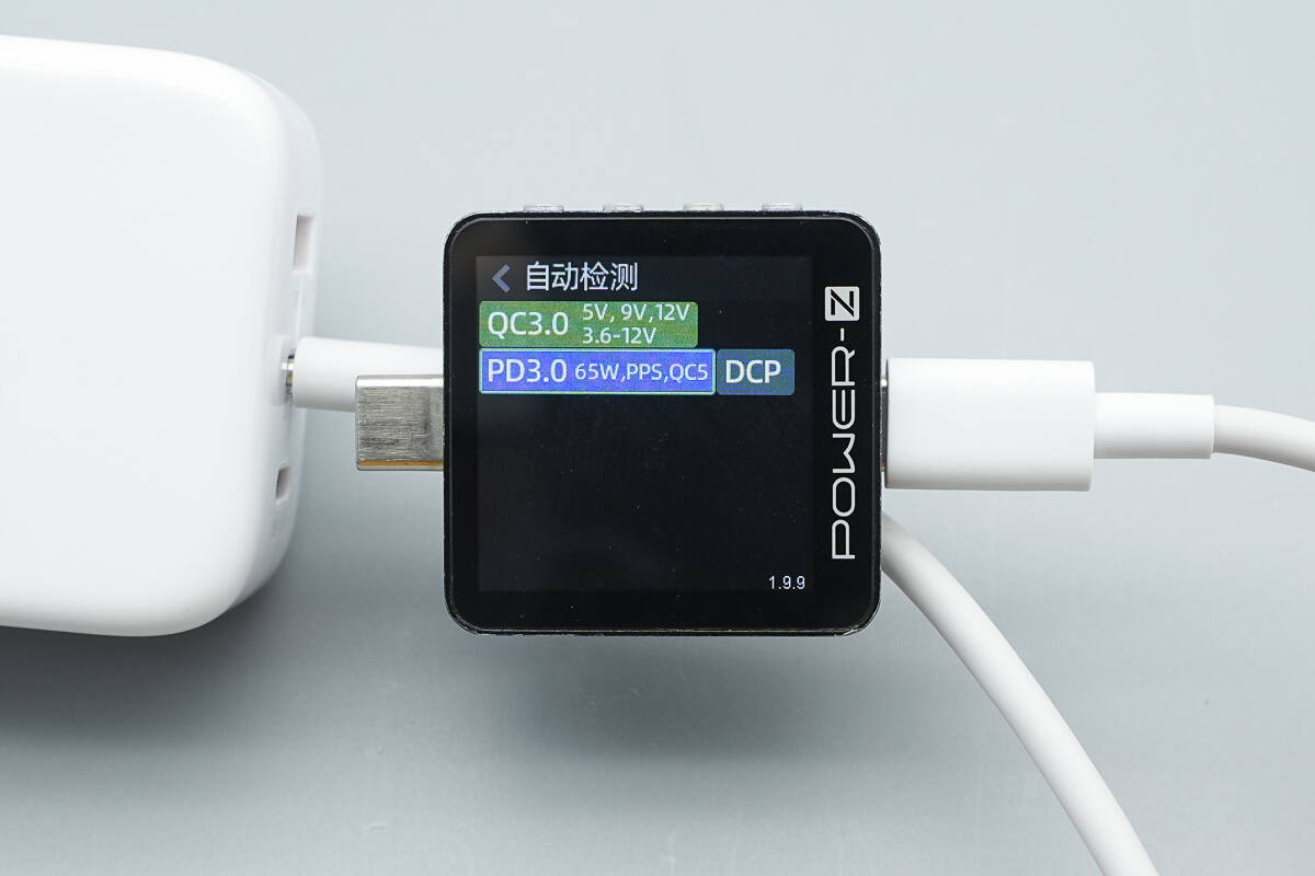
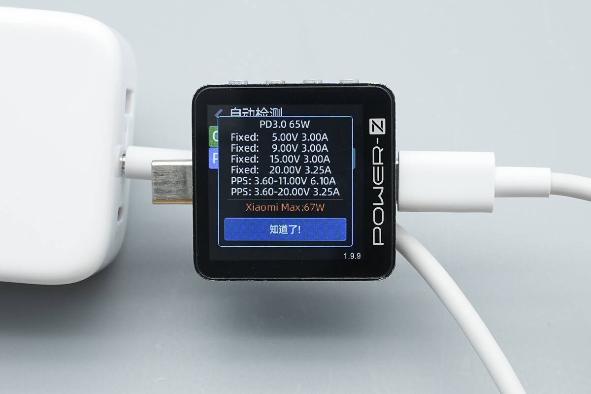
ChargerLAB POWER-Z KM003C shows that the USB-C1 supports QC3.0/5, PD3.0, PPS, and DCP protocol.
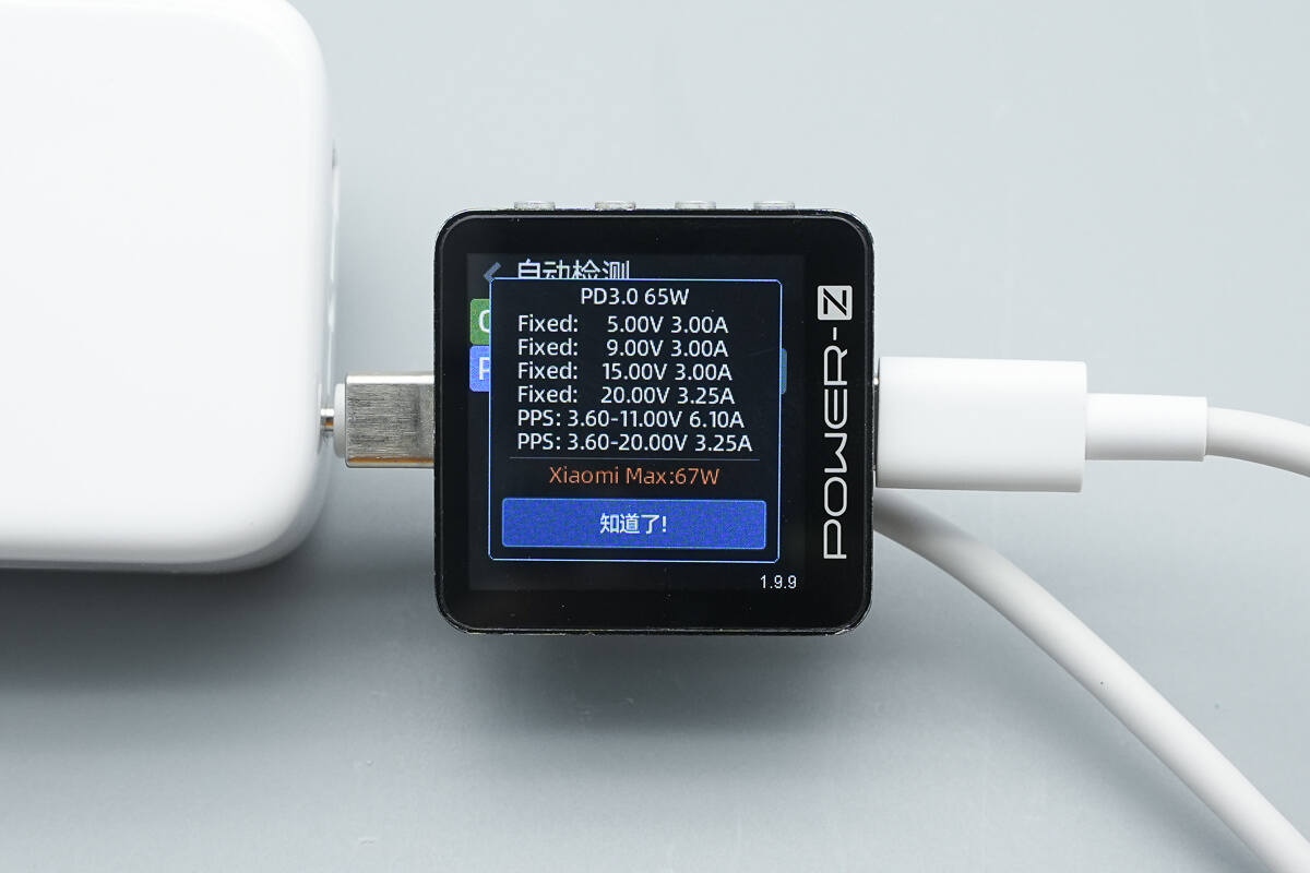
It has four fixed PDOs of 5V3A, 9V3A, 15V3A, 20V3.25A, as well as two sets of PPS, which are 3.6-11V6.1A and 3.6-20V3.25A. It also supports Xiaomi’s 67W Surge fast charging.
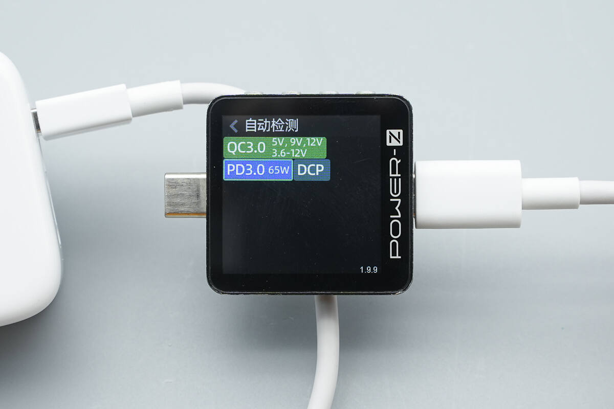
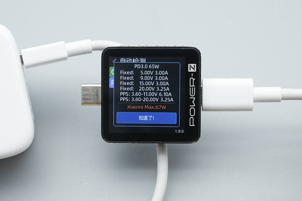
The USB-C2 port supports the same protocols as the USB-C1 port.
The PDO message is the same as well.
The USB-A port is a Xiaomi-customized type, supporting QC 3.0, PD 3.0, and DCP charging protocols.
The PDO message results are the same as those of the previous two USB-C ports.
Teardown
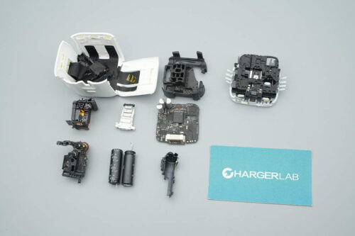
Next, let's take it apart to see its internal components and structure.
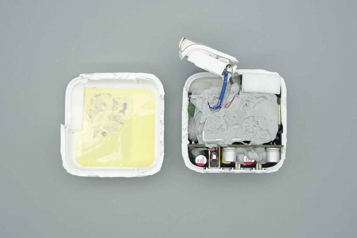
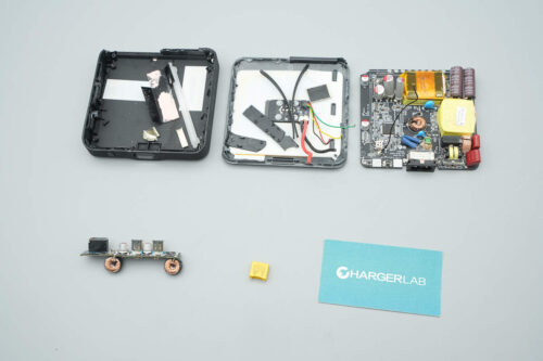
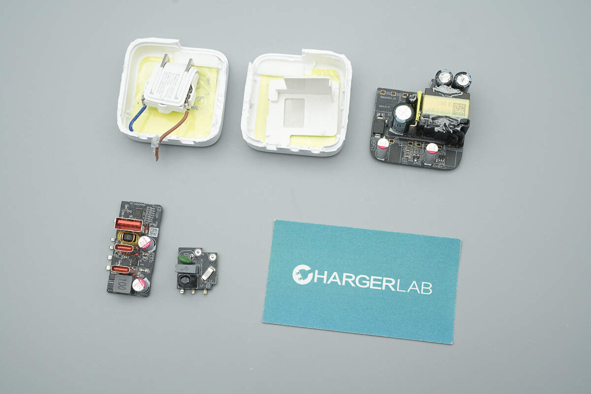
Cut open the housing welded by ultrasonic welding.
The inner side of the cover is lined with a graphite thermal pad and insulating tape.
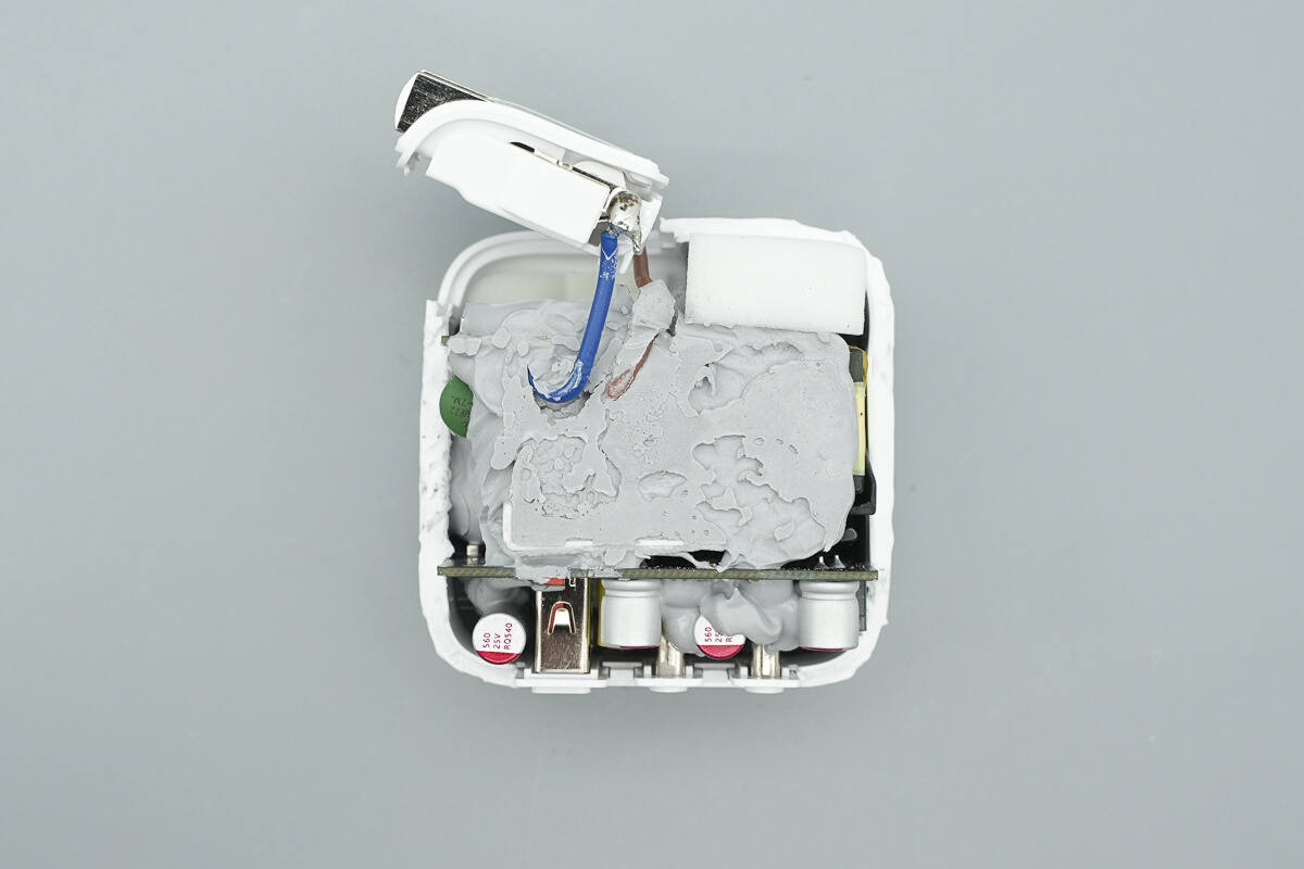
The interior is extensively filled with thermal adhesive.
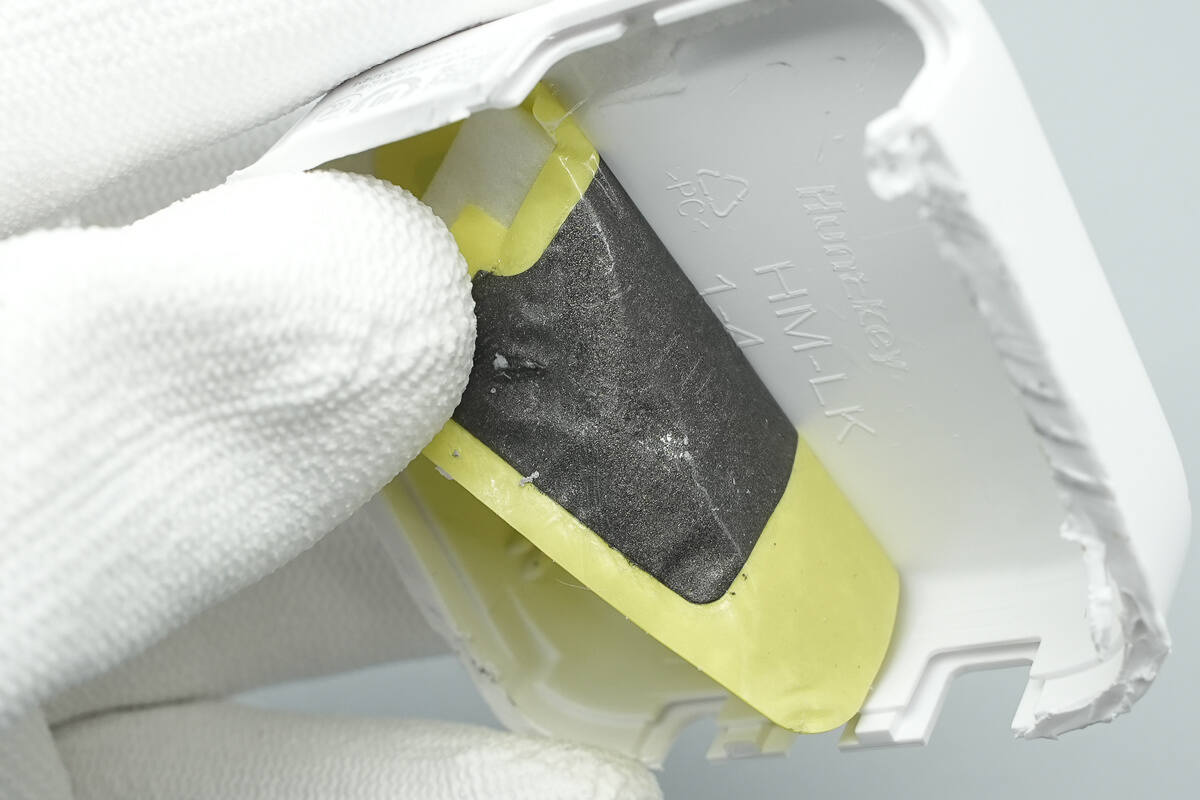
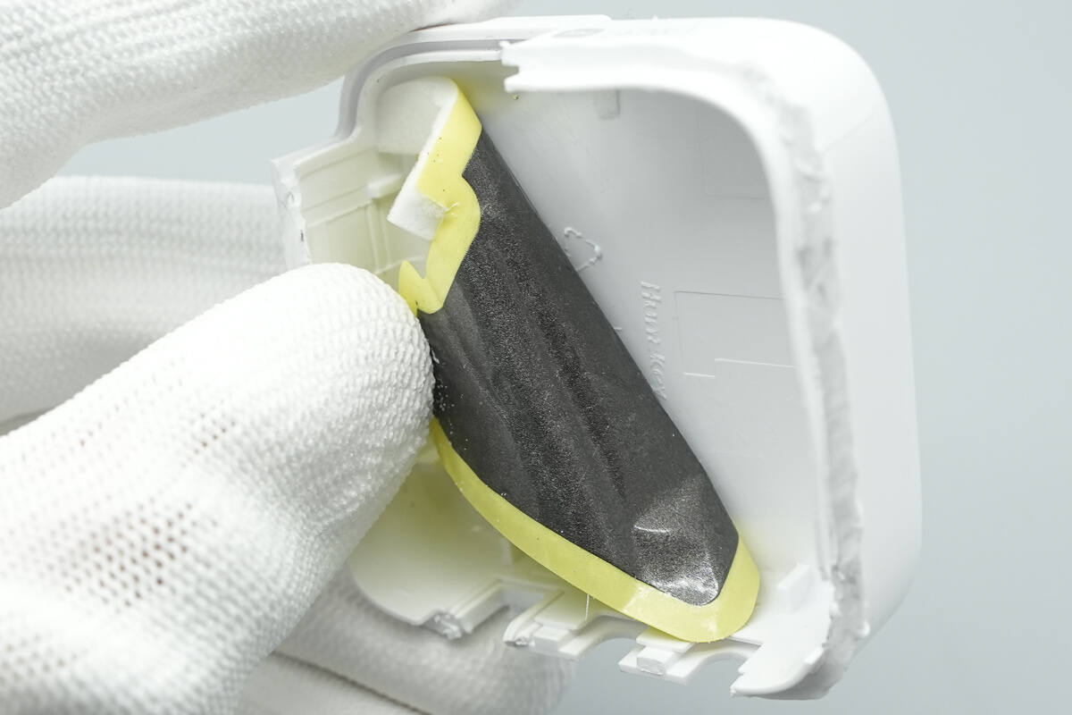
The PCBA module is removed. The other half of the housing is also lined with a graphite thermal pad and insulating tape. The enclosure is made of flame-retardant PC material. Additionally, the "HuntKey" marking on the housing indicates that the charger is manufactured by Shenzhen Huntkey Electric Co., Ltd.
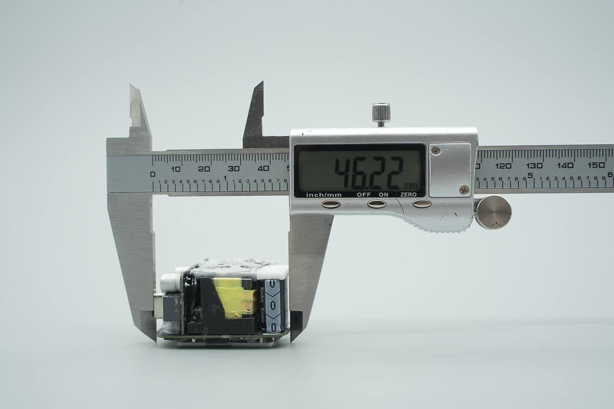
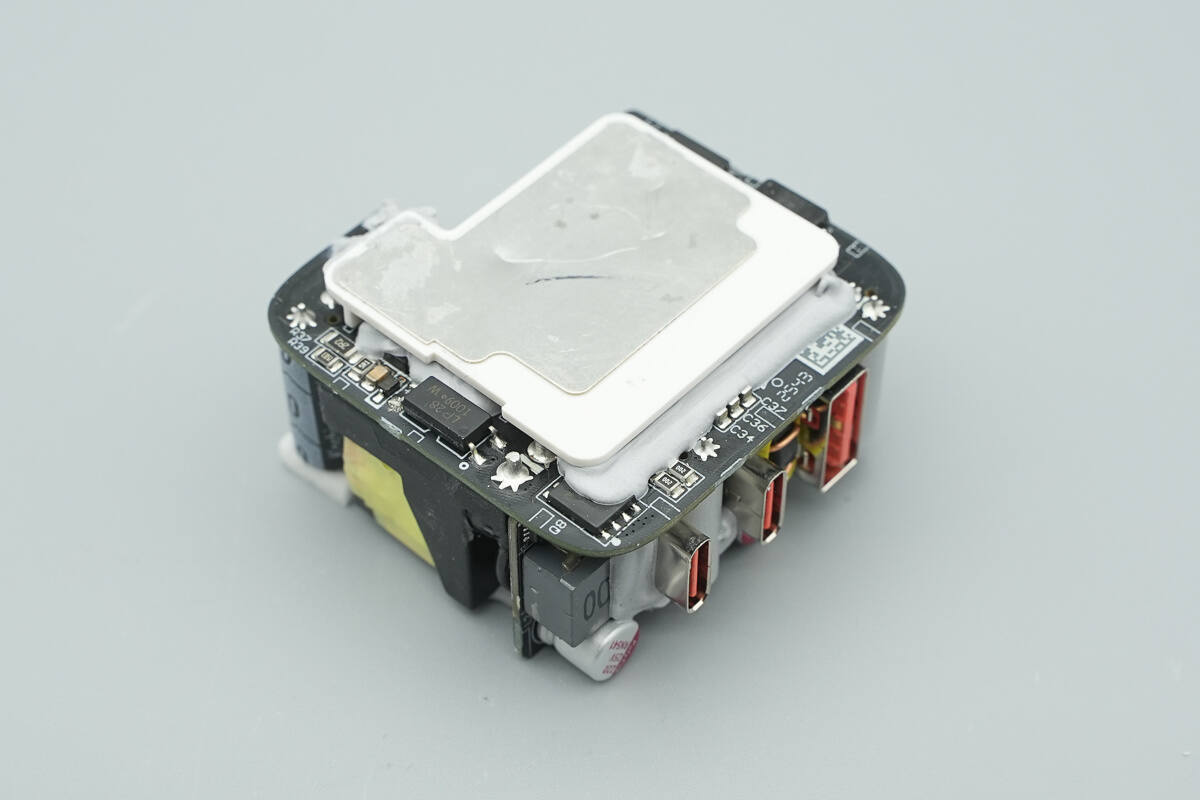
The length of the PCBA module is about 46.22 mm (1.82 inches).
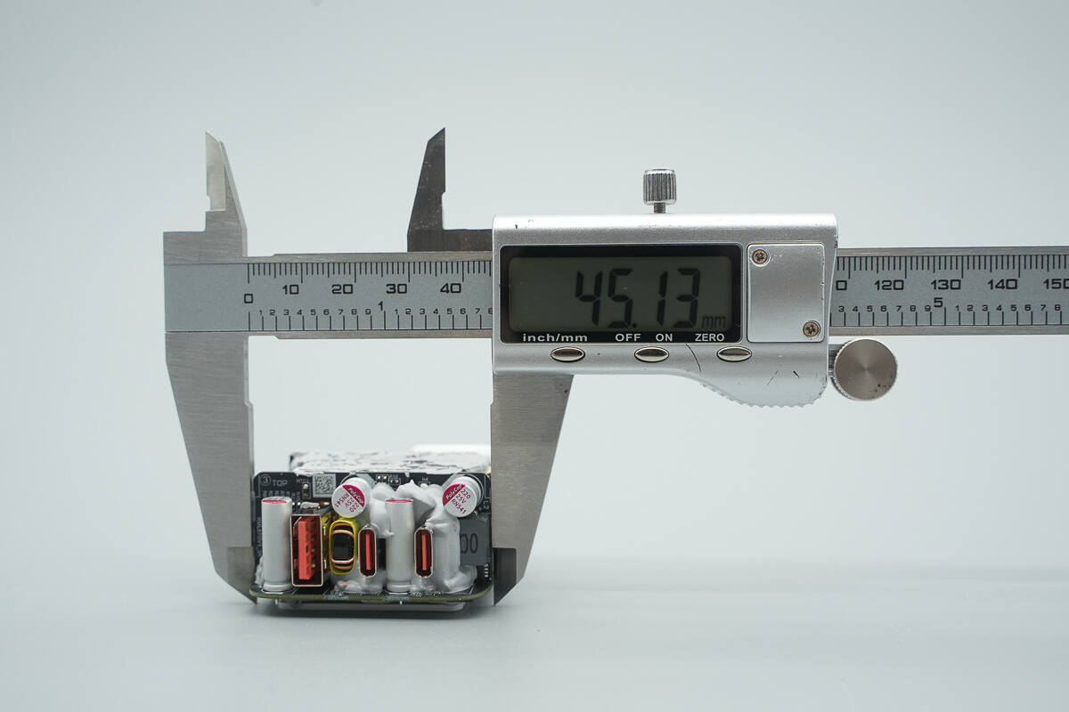
The width is about 45.13 mm (1.78 inches).
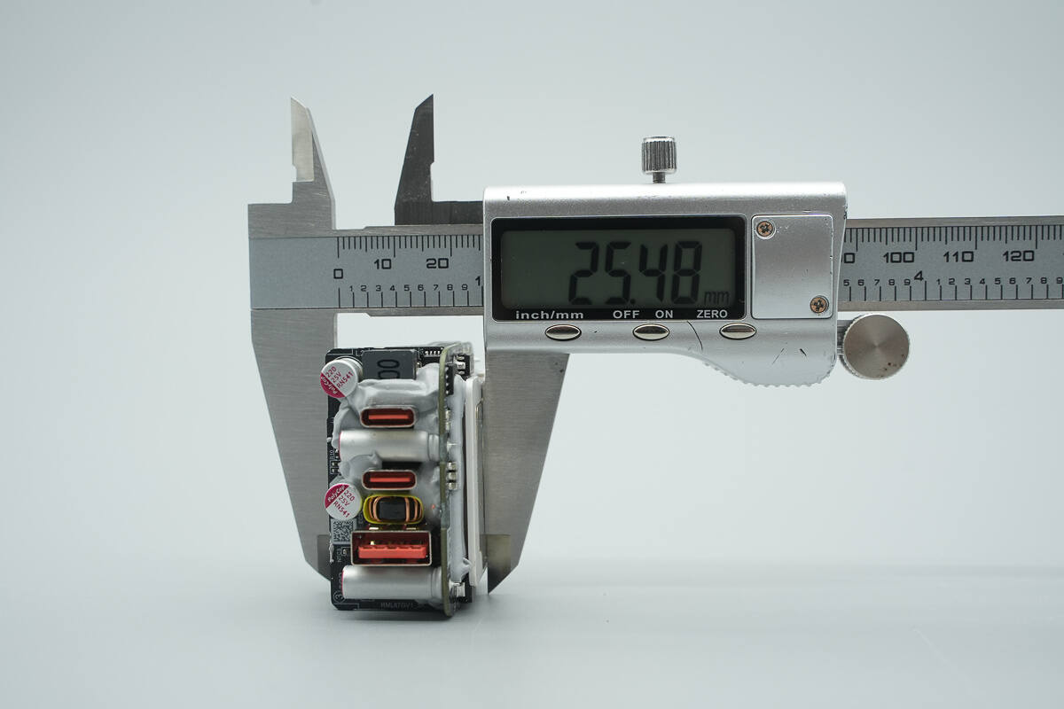
The thickness is about 25.48 mm (1.0031 inches).
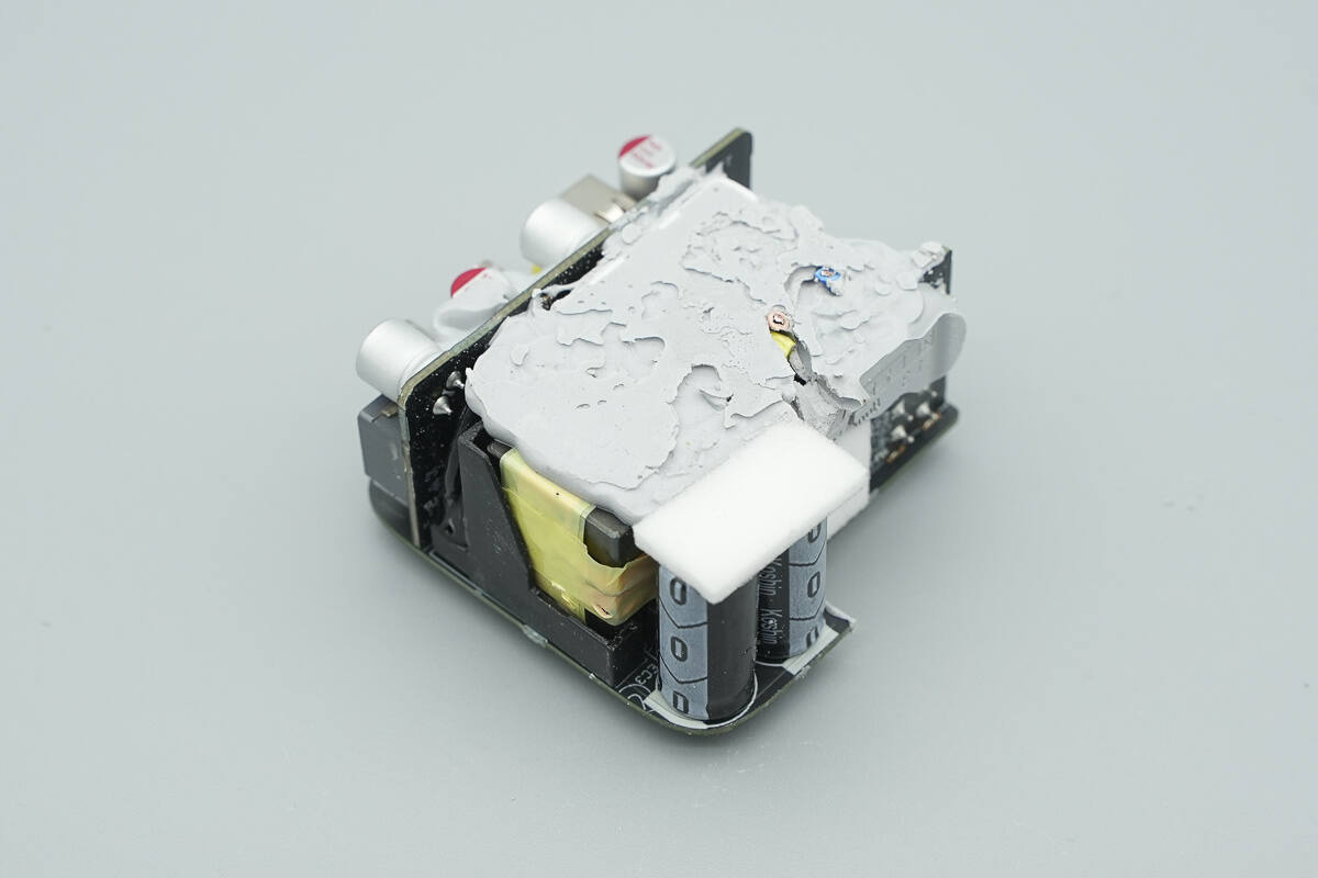
The front side of the PCBA module is extensively filled with thermal adhesive.
The bottom is covered with a plastic plate and a heatsink.
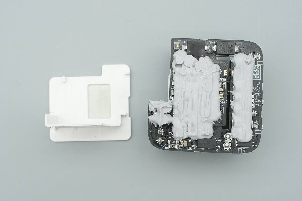
The plastic plate also serves to isolate the primary and secondary circuits.
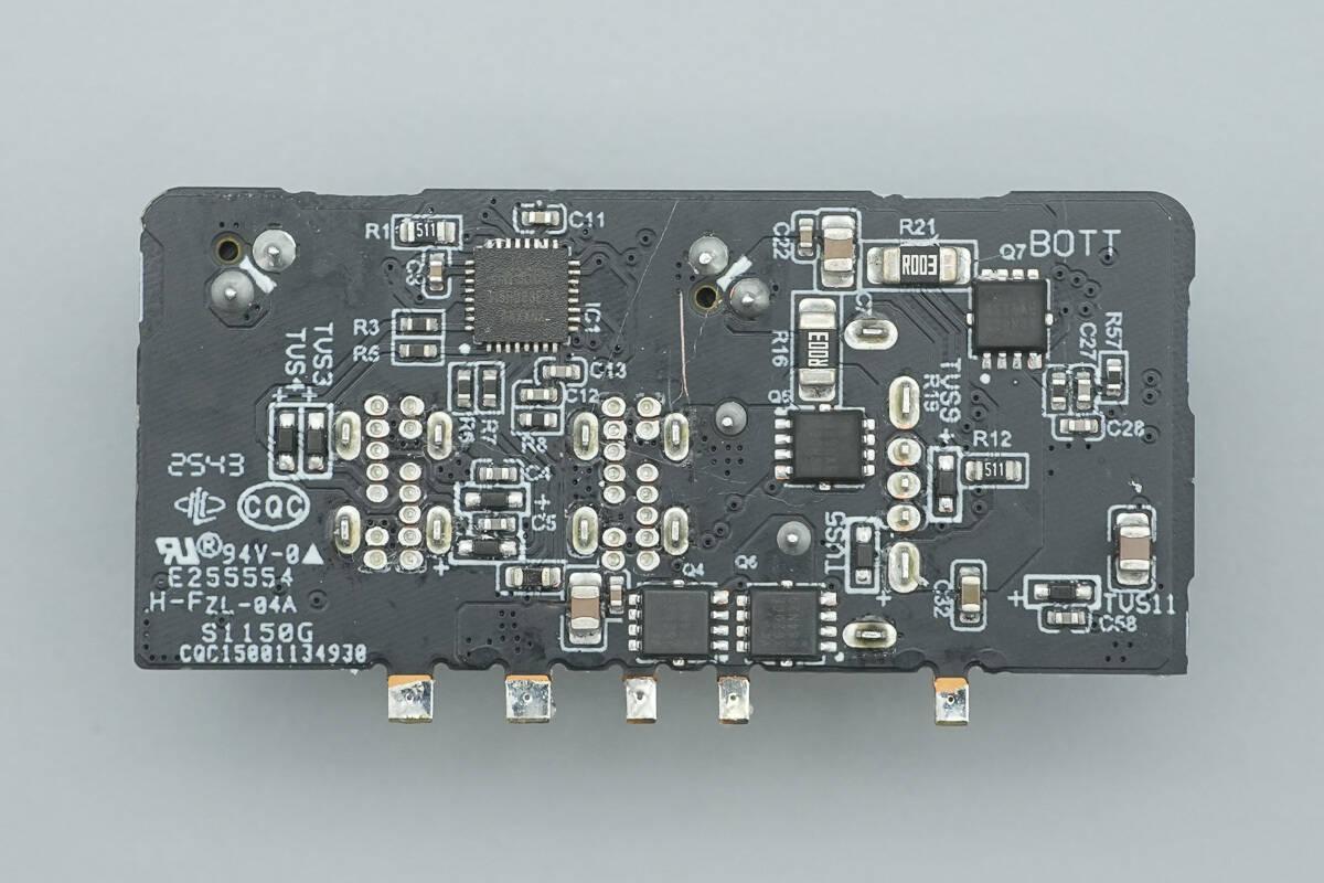
Remove the thermal adhesive. The front side of the module has a compact component layout, with small PCBs installed at both the front and rear ends.
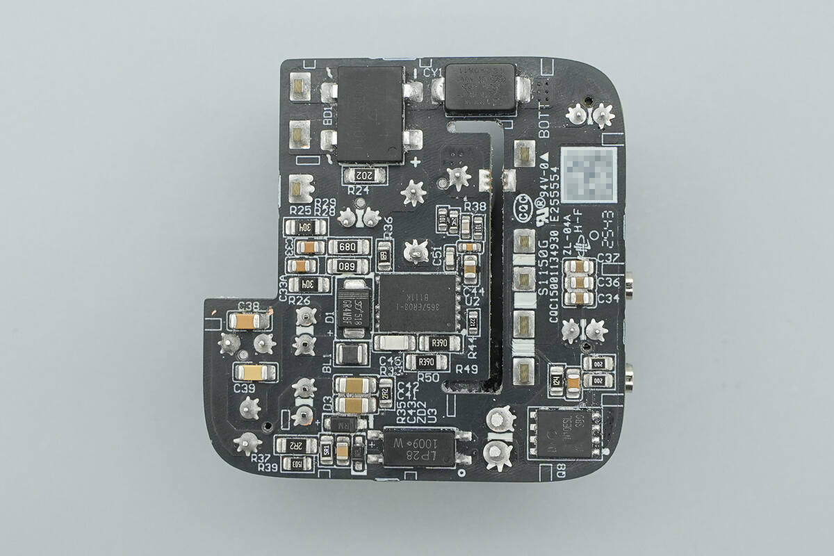
The back side contains a bridge rectifier, a master control chip, an optocoupler, an SMD Y capacitor, and a synchronous rectifier.
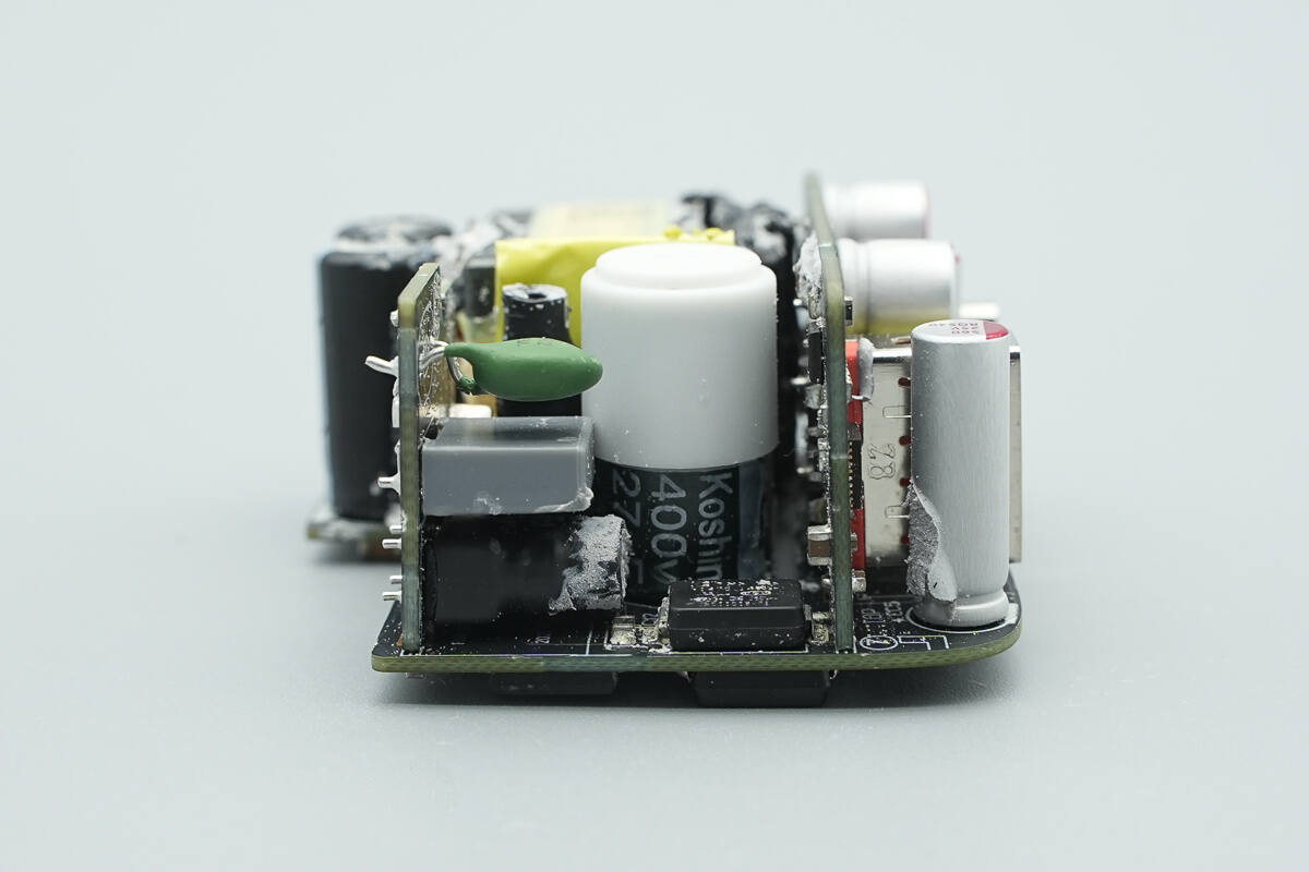
A small input PCB is soldered on this side.
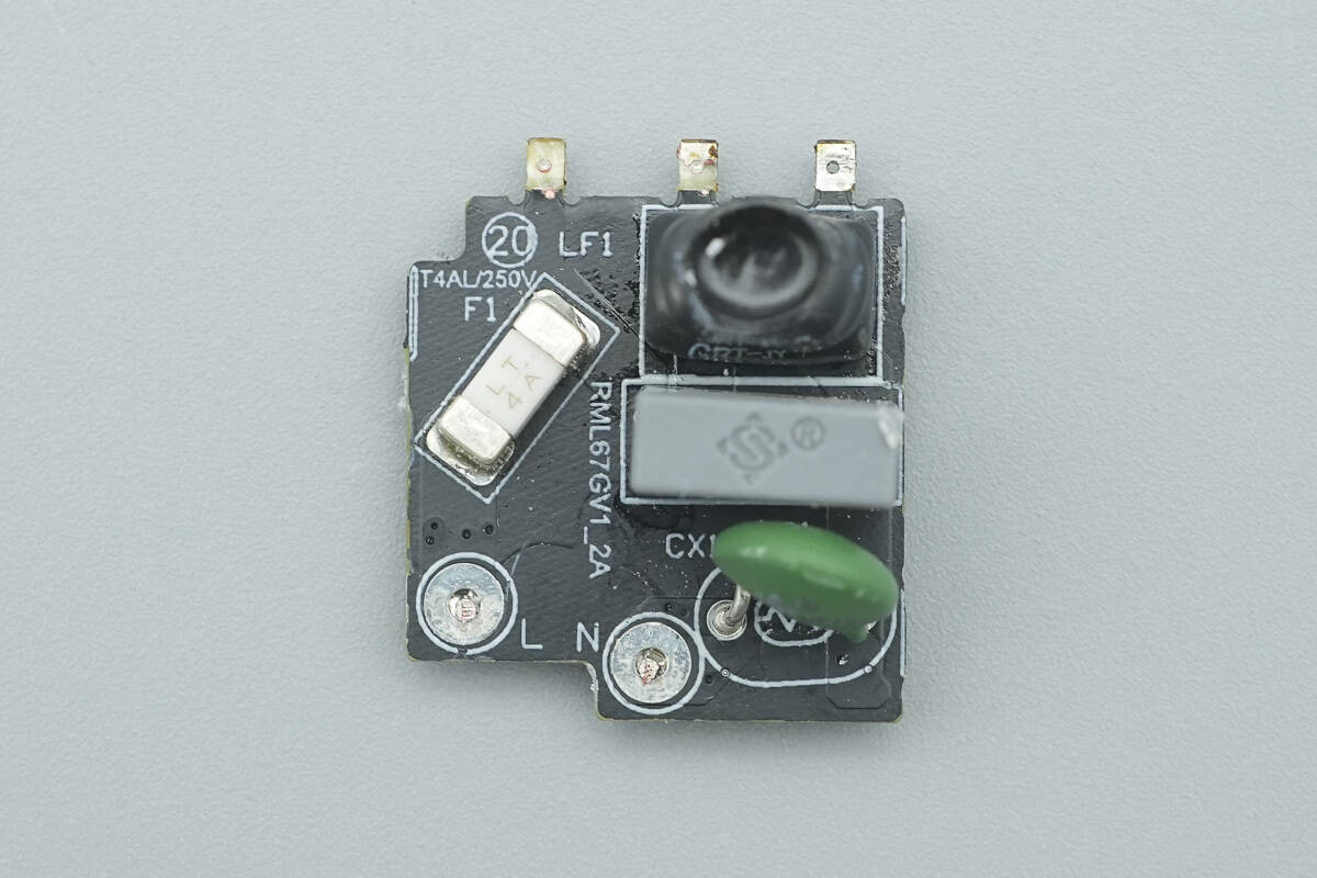
The input PCB is removed, revealing an SMD fuse, NTC thermistor, safety X2 capacitor, and common mode choke on the front side.
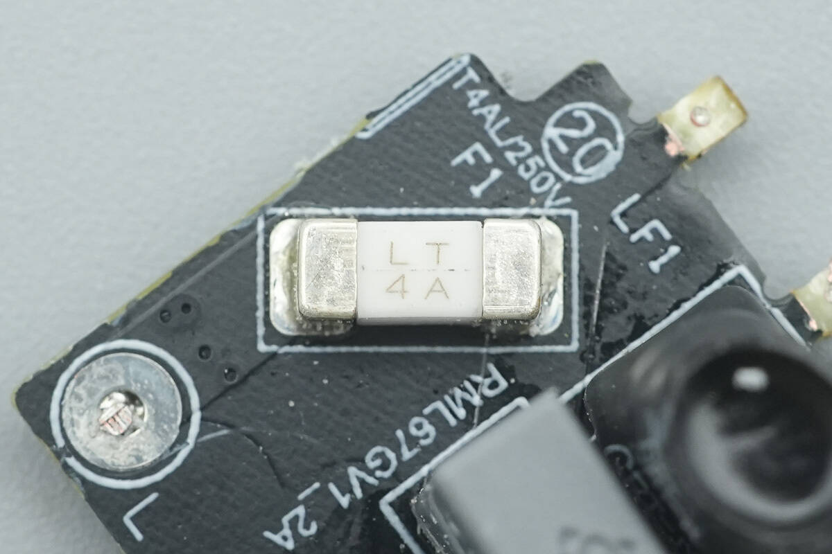
The SMD fuse is rated at 4 A.
The NTC thermistor is used to suppress inrush current at power-up.
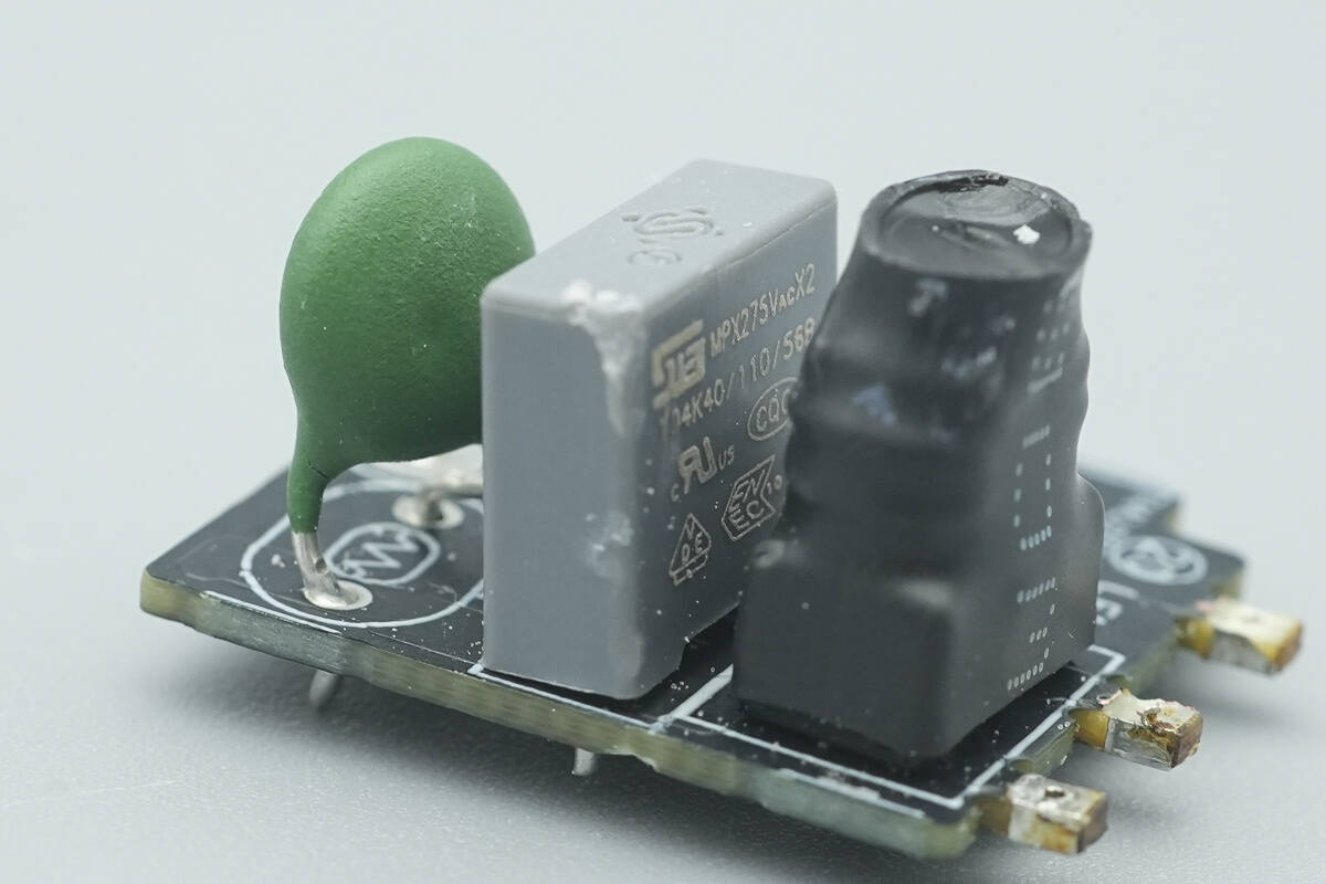
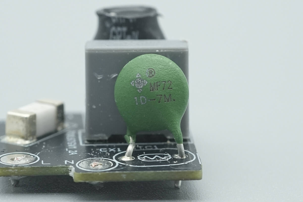
The safety X2 capacitor is from STE, with a capacitance of 0.1 μF.
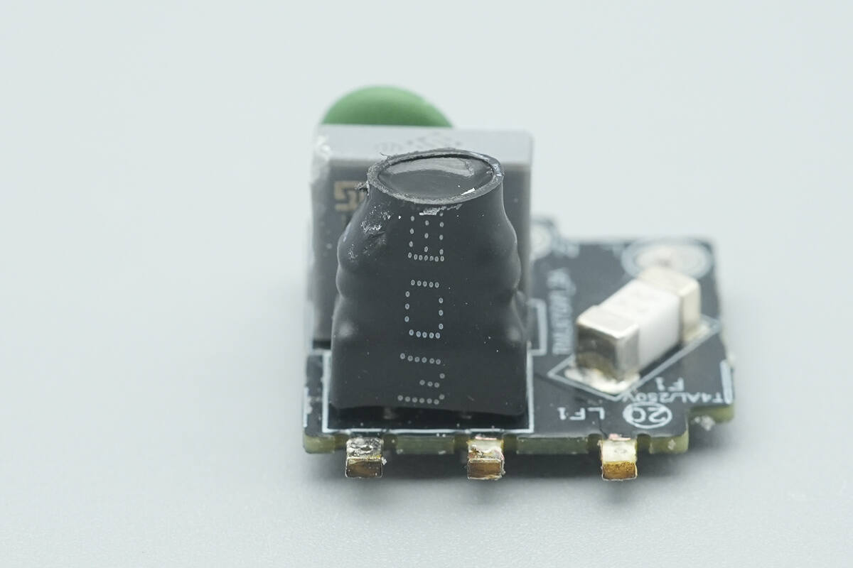
The common mode choke is used to filter EMI interference and is insulated with a heat-shrink sleeve for protection.
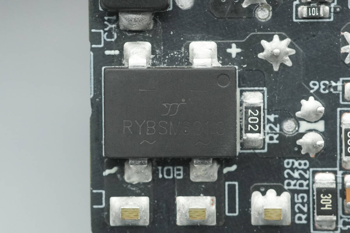
The bridge rectifier is from YJ, model RYBSM6010. It is a fast-recovery bridge rectifier rated at 1000 V/6 A and uses a YBS3 package.
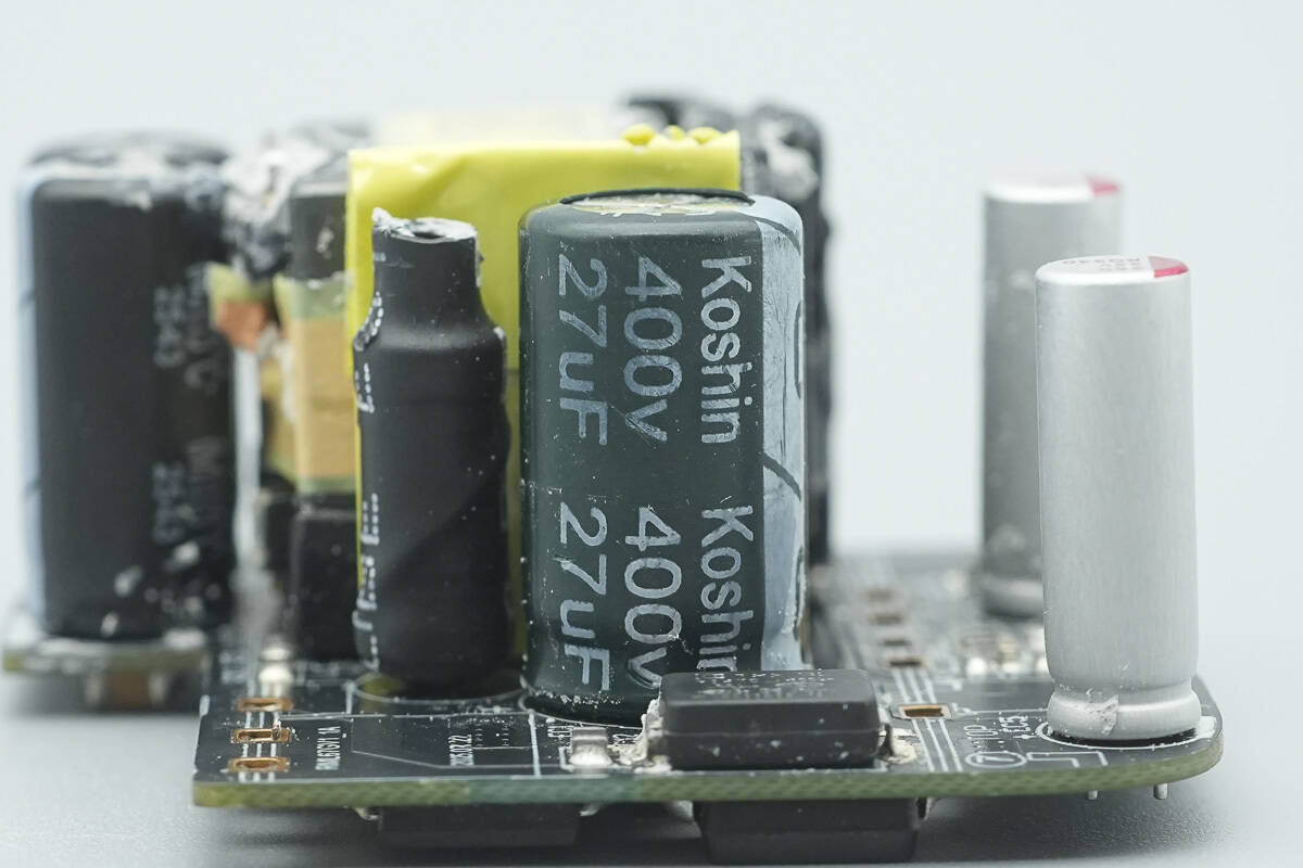
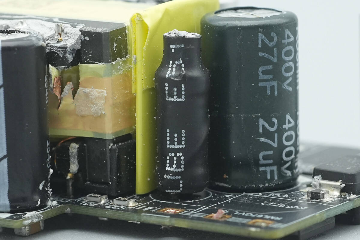
The high-voltage electrolytic capacitor is from Koshin, rated at 400 V, 27 μF.
The I-shaped inductor is insulated with a heat-shrink sleeve.
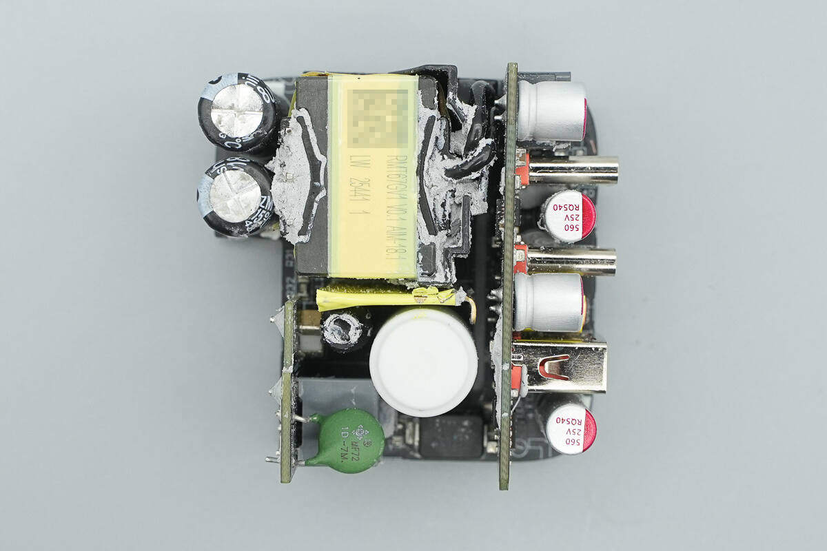
At the front end of the module, there are two high-voltage filtering electrolytic capacitors. A heatsink is soldered to the right side of the transformer and is wrapped with insulating tape.
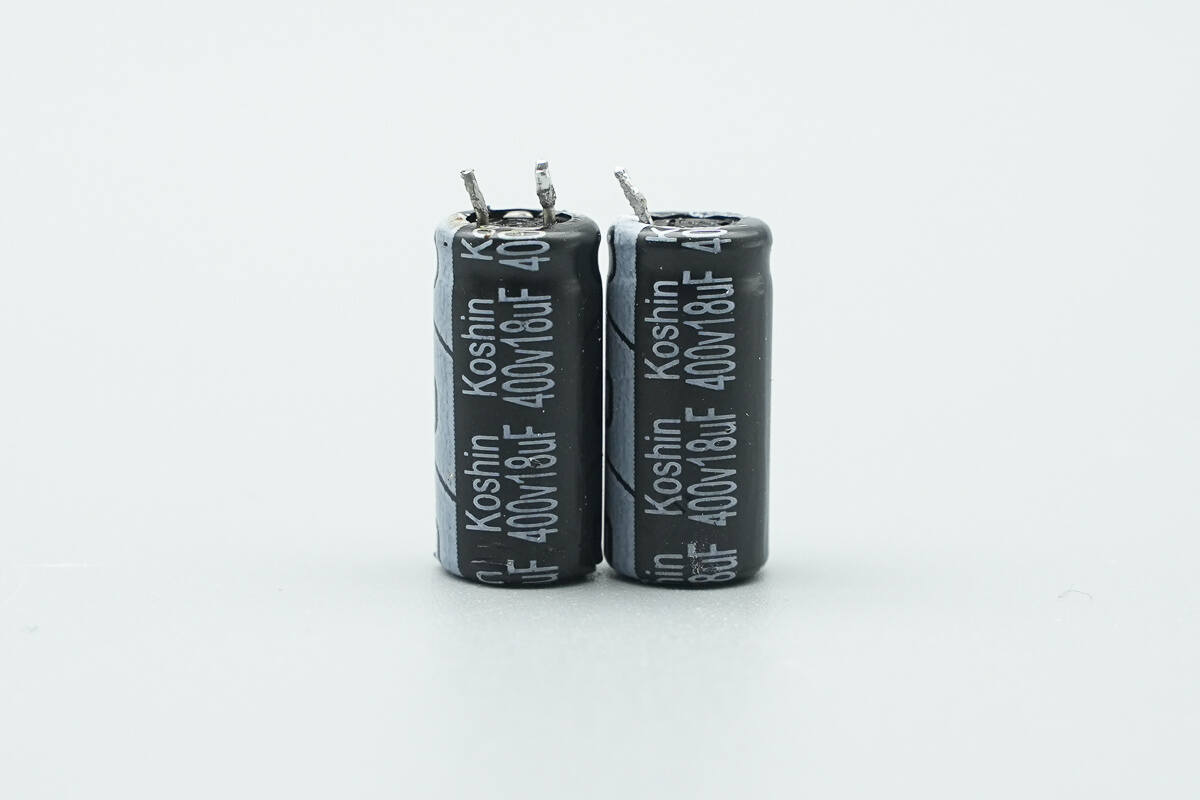
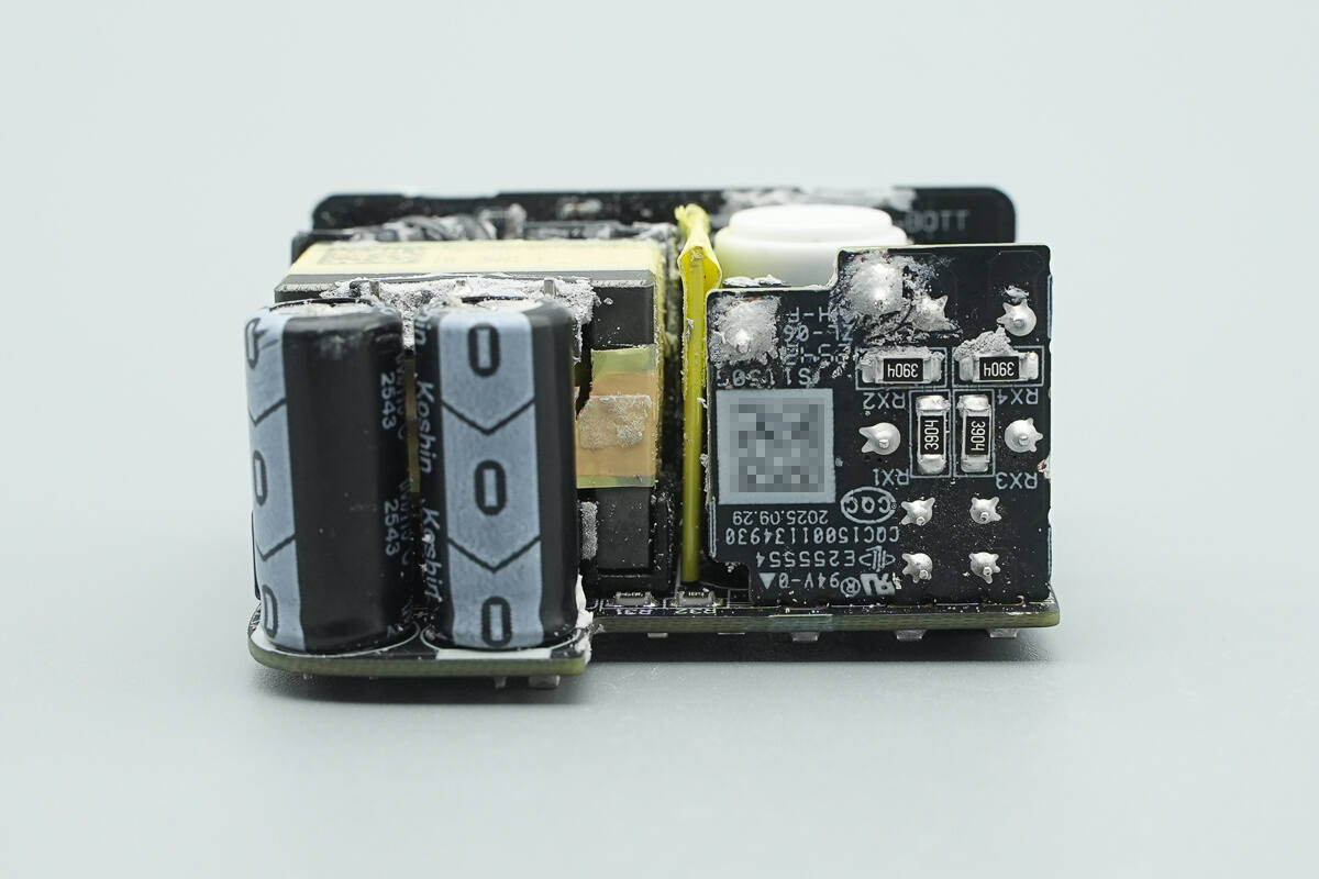
The two high-voltage filtering electrolytic capacitors are from Koshin, each rated at 400 V, 18 μF.
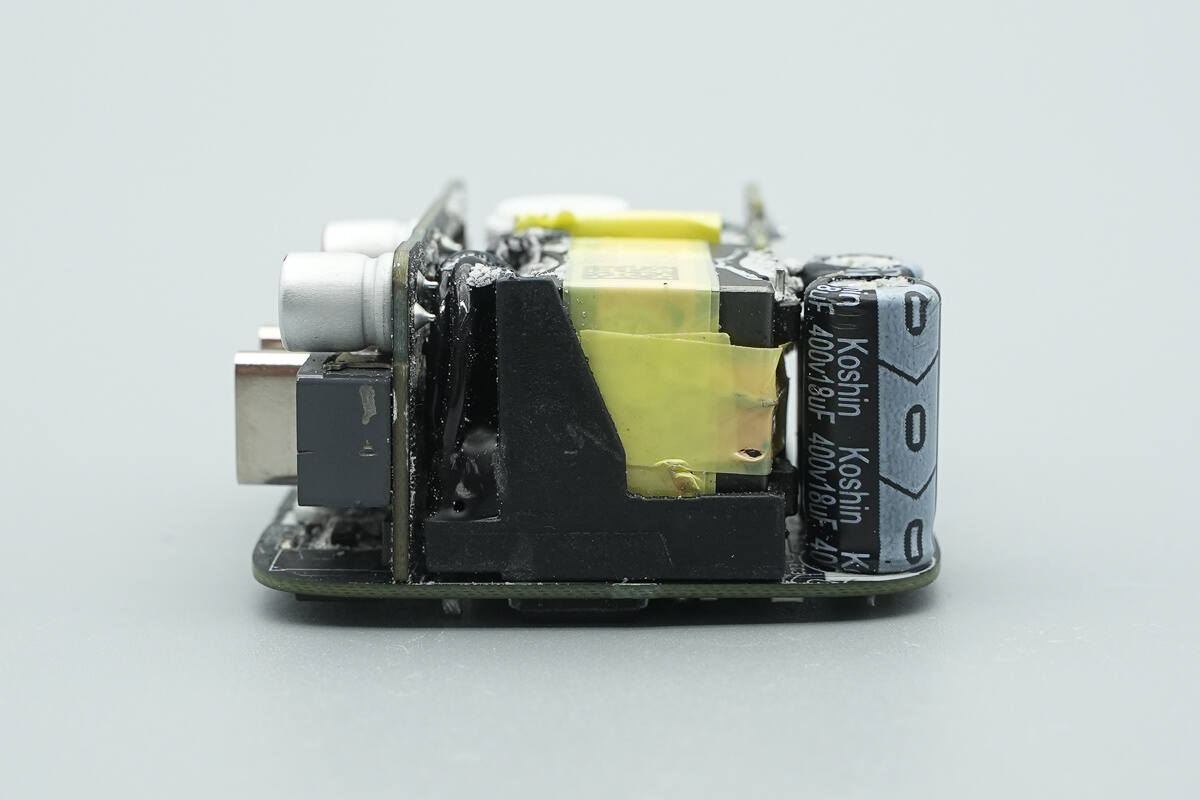
On the other side of the module, there is a transformer, reinforced with a plastic bracket around it.
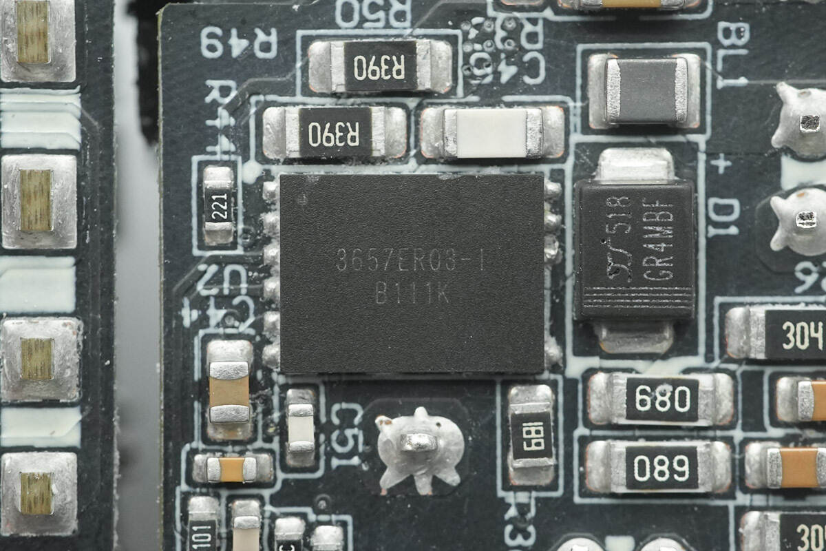
The master control chip is from HYASiC, model HYC3657. It is an intelligent digital multi-mode flyback converter integrating a 700 V enhancement-mode GaN power device. The chip features a built-in 700 V high-voltage startup circuit and employs intelligent digital multi-mode control technology, enabling efficient operation in burst mode, PFM, DCM, and quasi-resonant (QR) modes based on peak current mode control.
HYC3657 optimizes EMI through switching frequency dithering and combines adaptive GaN gate drive to achieve an optimal balance between switching loss and EMI performance. It offers comprehensive protection functions, including output overvoltage protection, transformer saturation protection, VCC overvoltage protection, overload protection, input undervoltage/overvoltage protection, overtemperature protection, and line-voltage feedforward compensation, ensuring high system reliability. The chip’s standby power consumption is below 20 mW, and it is available in a DFN6×8 package.
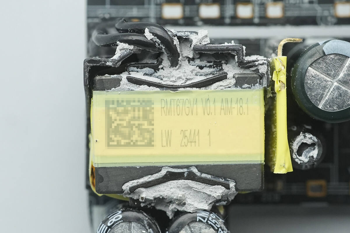
Close-up of the transformer.
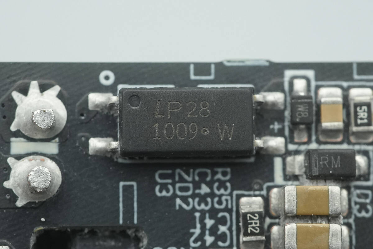
The 1009 optocoupler is used for output voltage feedback.
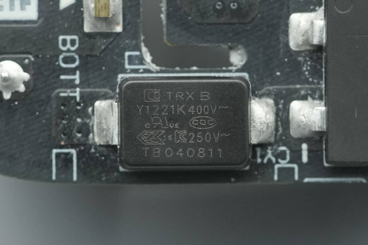
The SMD Y capacitor is from TRX, part number TMY1221K. Its compact size and light weight make it well-suited for high-density power products such as GaN fast chargers.
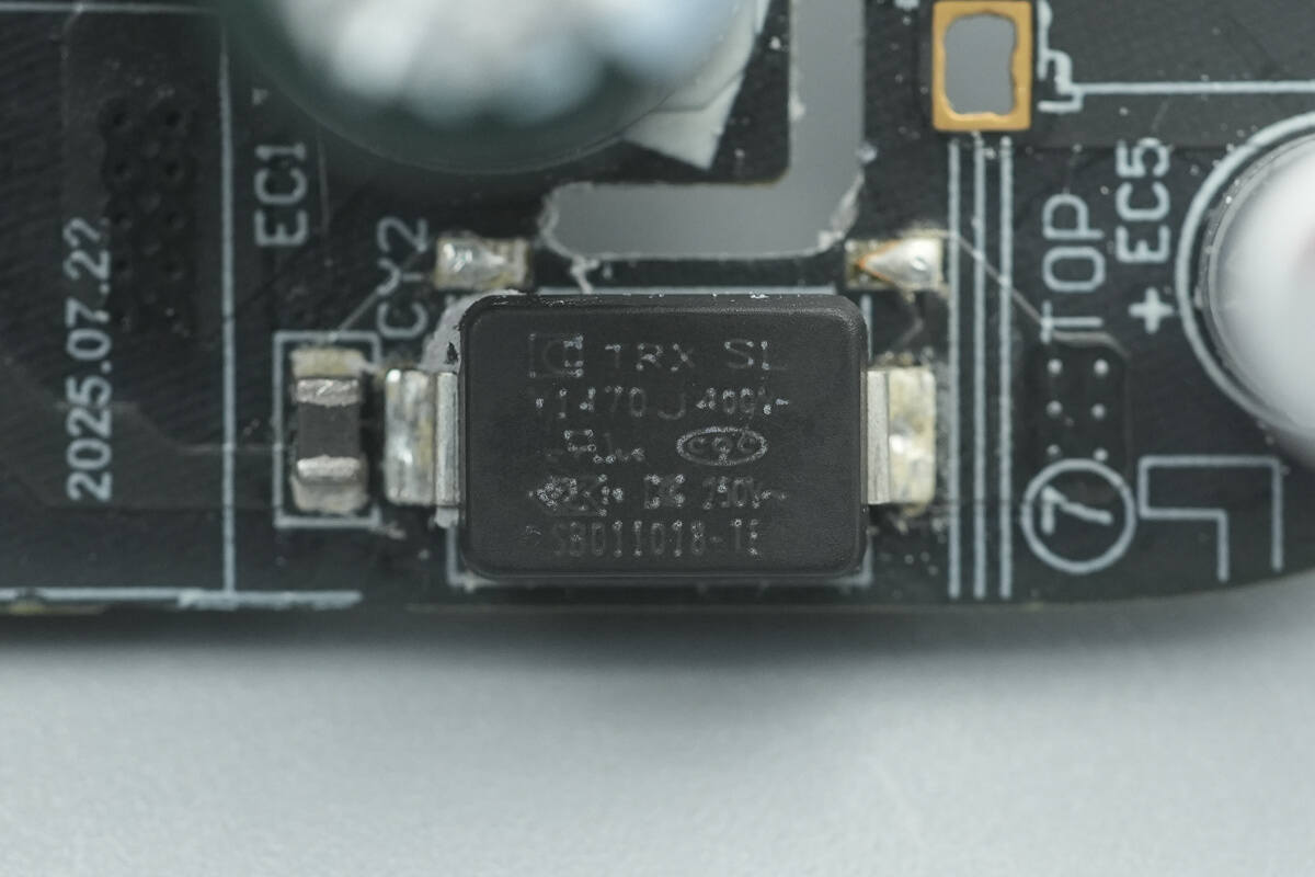
The other SMD Y capacitor is also from TRX, with part number TMY1470J.
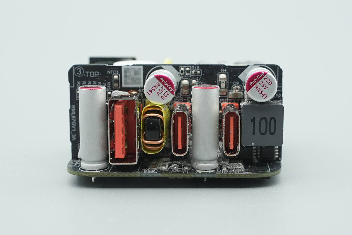
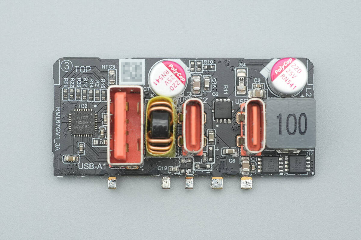
A small PCB is soldered on the output side.
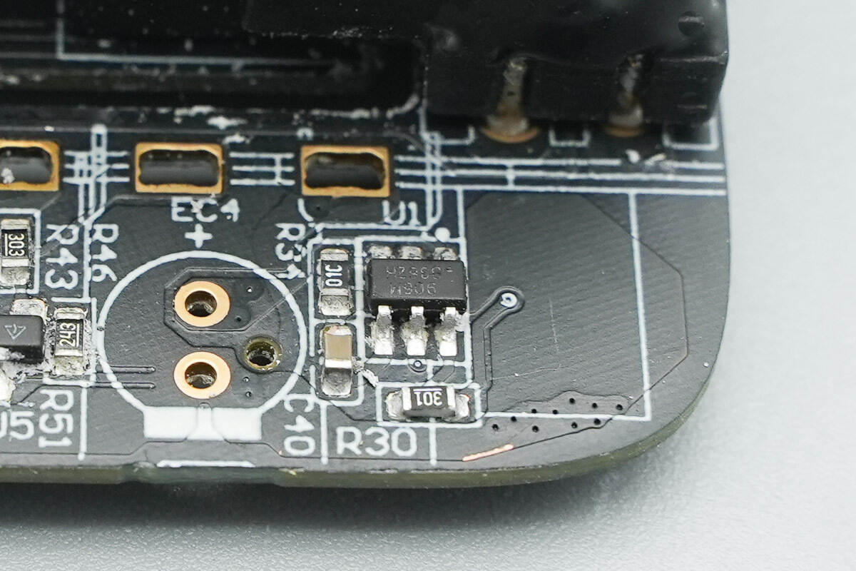
The small PCB is removed, revealing that the secondary side on the main board has a synchronous rectifier controller.
A synchronous buck MOSFET, a buck inductor, a solid capacitor, a buck control IC, and VBUS MOSFETs on the front side.
On the back side are a buck protocol chip, synchronous buck MOSFETs, and a VBUS MOSFET.
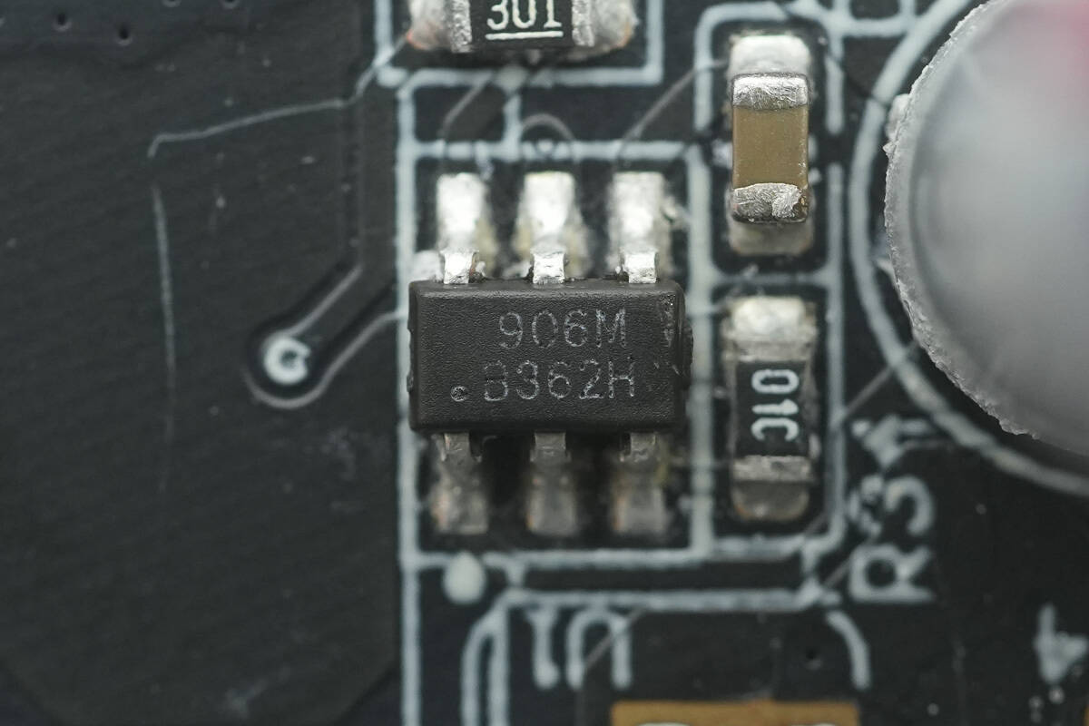
The synchronous rectifier controller is from HYASiC, model HYC906M.
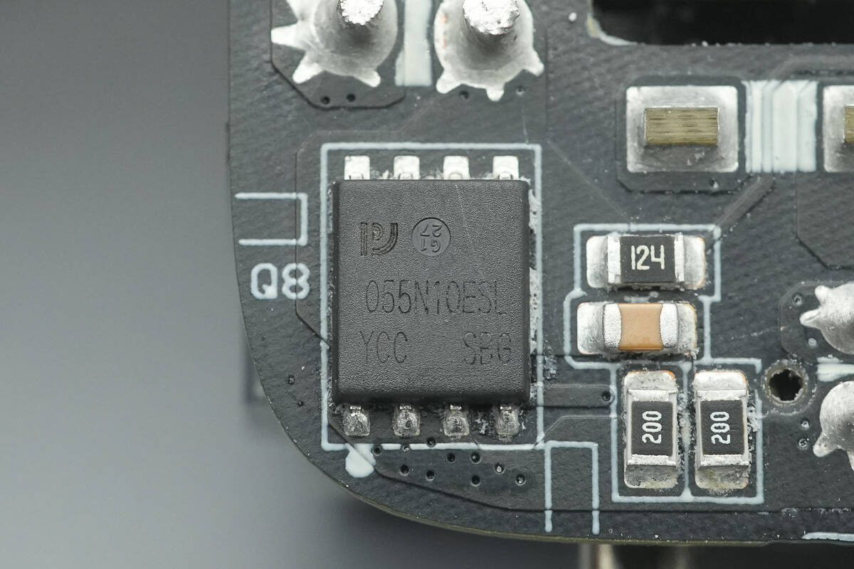
The synchronous rectifier is from PY, model PW055N10ESL, an N-MOSFET rated for 100 V with a 4.4 mΩ Rds(on), housed in a DFN 5×6 package.
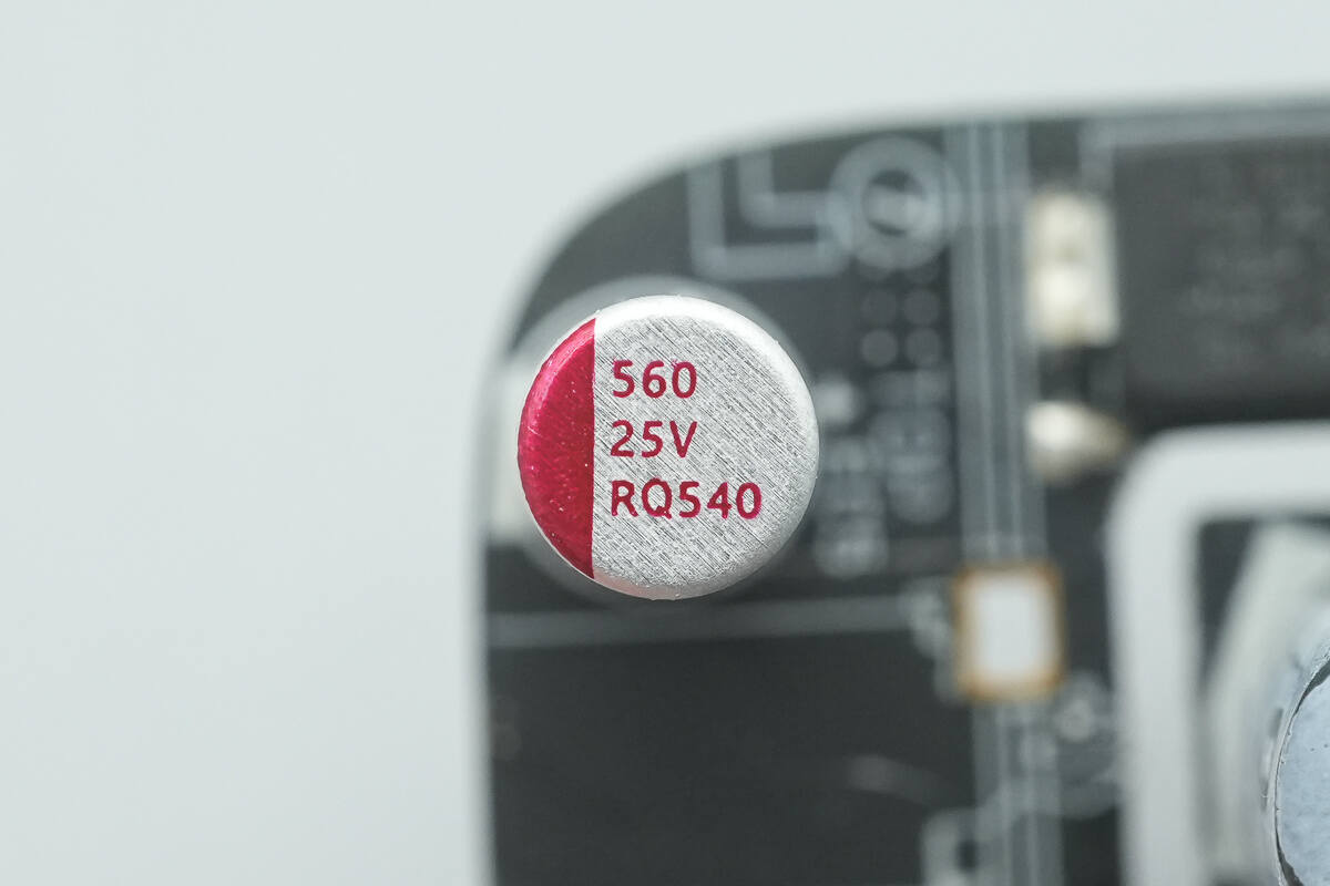
The output filter solid capacitor is rated at 25 V, 560 µF.
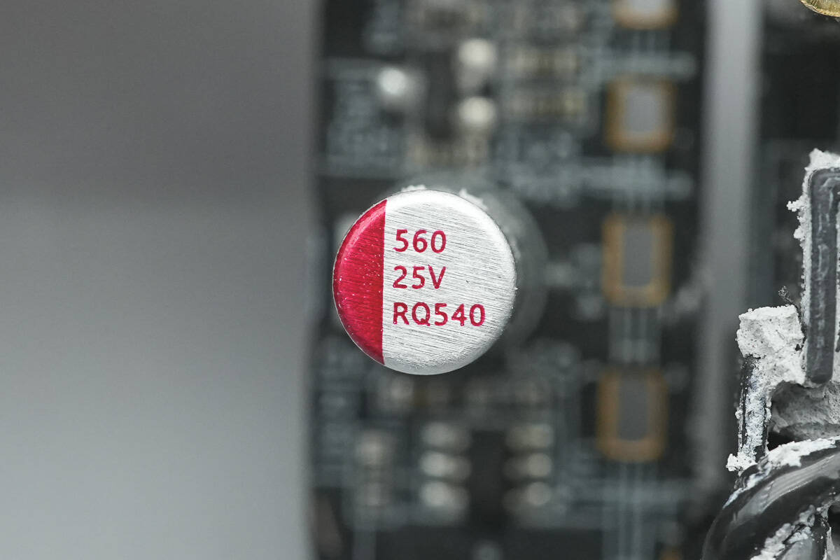
The other filter solid capacitor has the same specification.
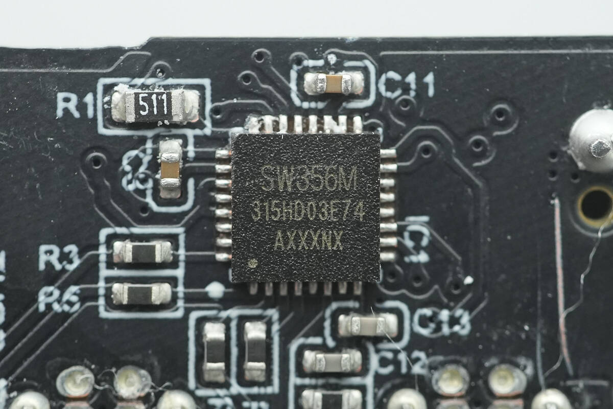
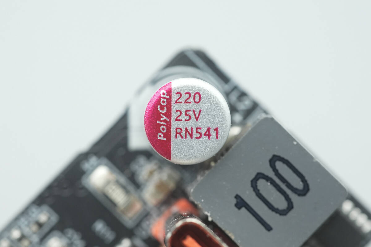
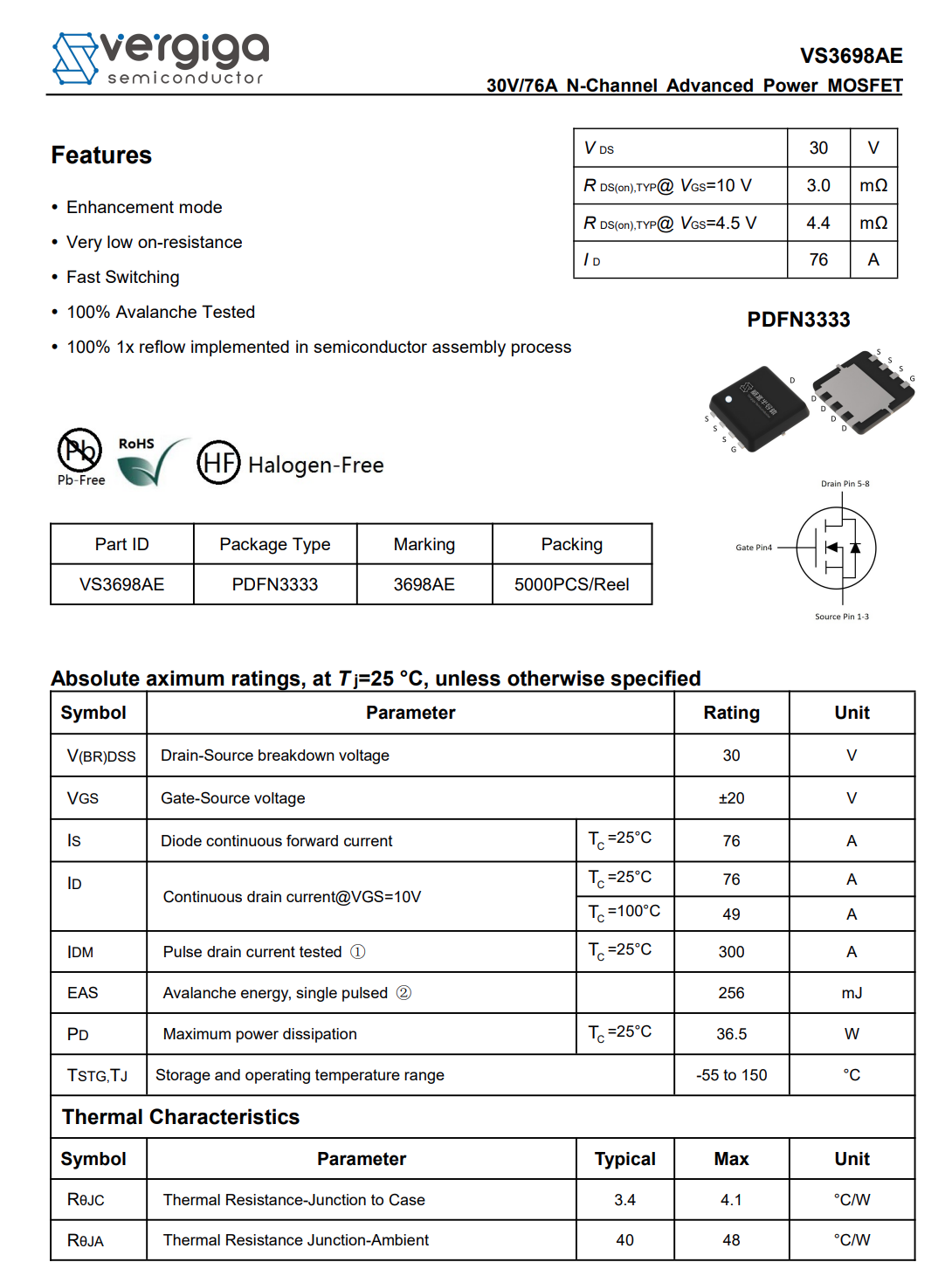
The USB-C1 port’s buck protocol chip is the SW356M from iSmartWare. It is an integrated 7A buck controller supporting 140 W (28 V @ 5 A) output power and multiple fast-charging protocols, including PD3.1, designed for C+C dual-port SoC applications.
The SW356M incorporates an ARM Cortex-M0 core and integrates Type-C interface logic, a PD3.1 PHY, UFC-S PHY, SCP/AFCP PHY, TFC-P PHY, and fast-charging protocol detection circuitry such as QC, PE, and SFCP. Only a small number of external components are required to build a complete high-performance dual-USB-C fast-charging solution.
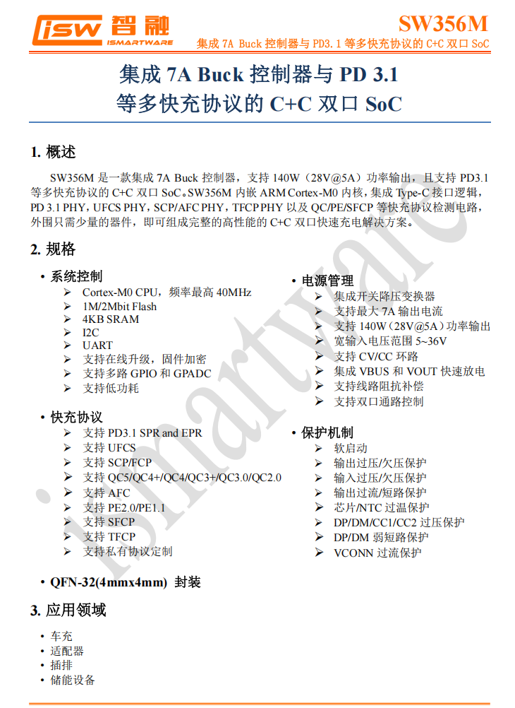
Here is the information about iSmartWare SW356M.
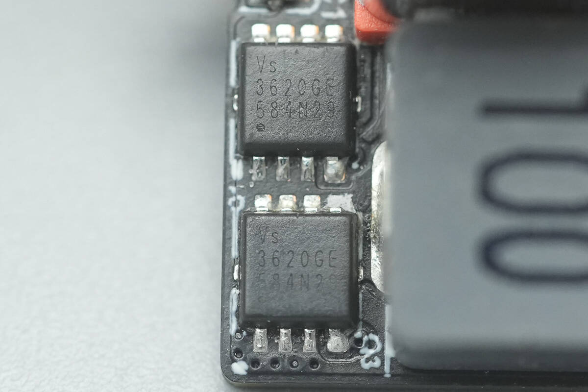
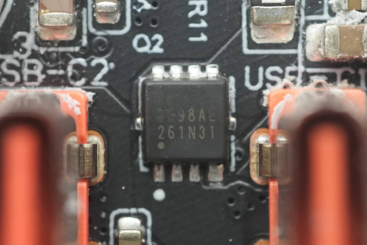
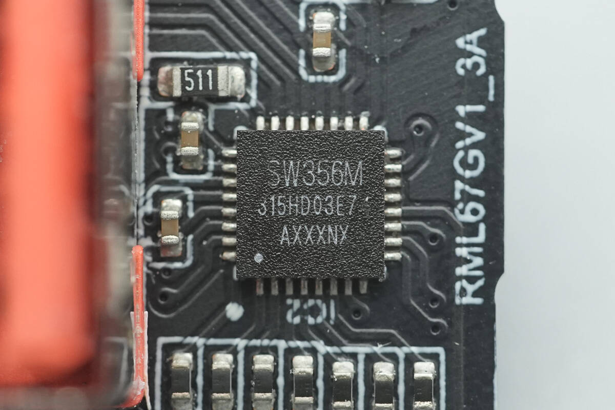
The paired synchronous buck MOSFETs are from Vergiga, model VS3620GEMC. They are 30 V N-MOSFETs with an Rds(on) of 4.9 mΩ and come in a PDFN3333 package.
Here is the information about Vergiga VS3620GEMC.
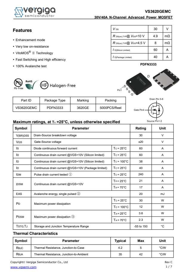
Close-up of the paired 10 µH buck inductor.
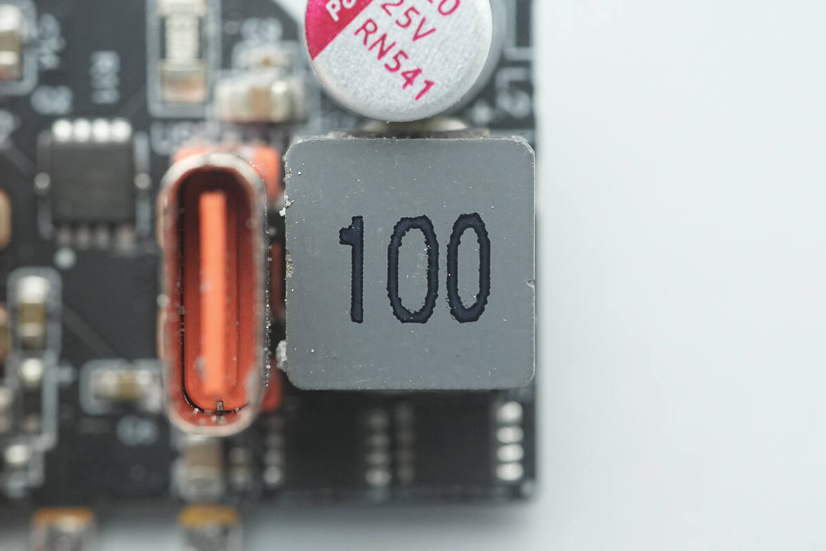
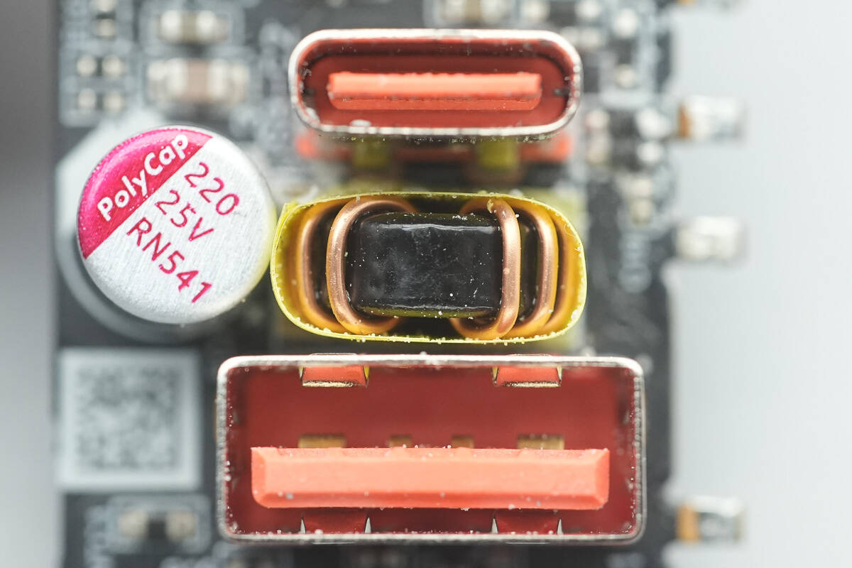
The buck output filter solid capacitor is from PolyCap, rated at 25 V, 220 µF.
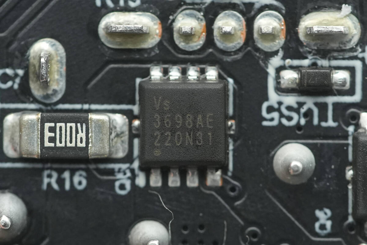
The VBUS MOSFET for the USB-C1 port is from Vergiga, model VS3698AE. It is a 30 V N-MOSFET with an Rds(on) of 3 mΩ, housed in a PDFN3333 package.
Here is the information about Vergiga VS3698AE.
The buck protocol chips for the USB-C2 and USB-A ports also use the iSmartWare SW356M.
The two synchronous buck MOSFETs also use the Vergiga VS3620GEMC.
The buck inductor is wrapped with insulating tape.
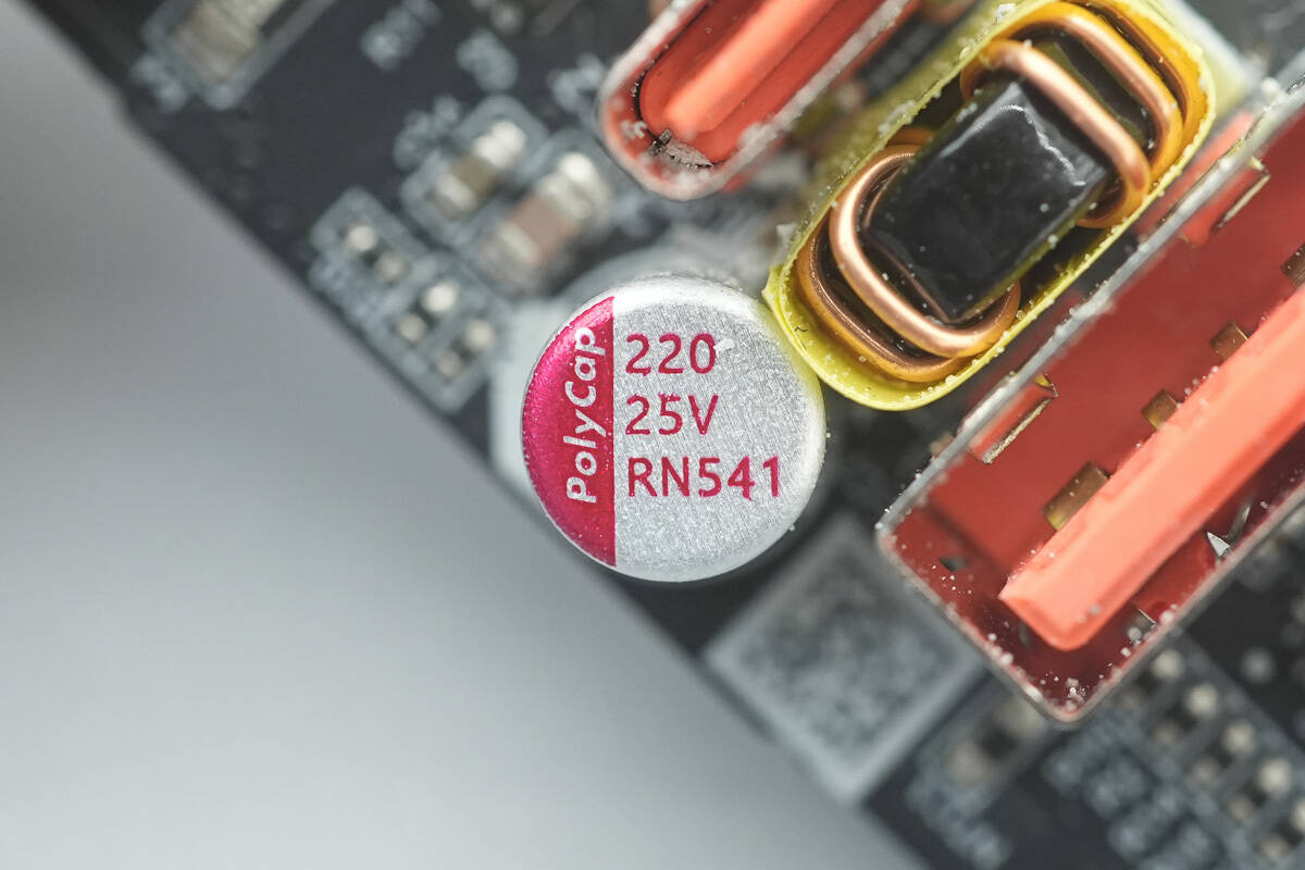
The buck output filter solid capacitor also comes from PolyCap, rated at 25 V, 220 µF.
The VBUS MOSFET for the USB-C2 port also uses the Vergiga VS3698AE.
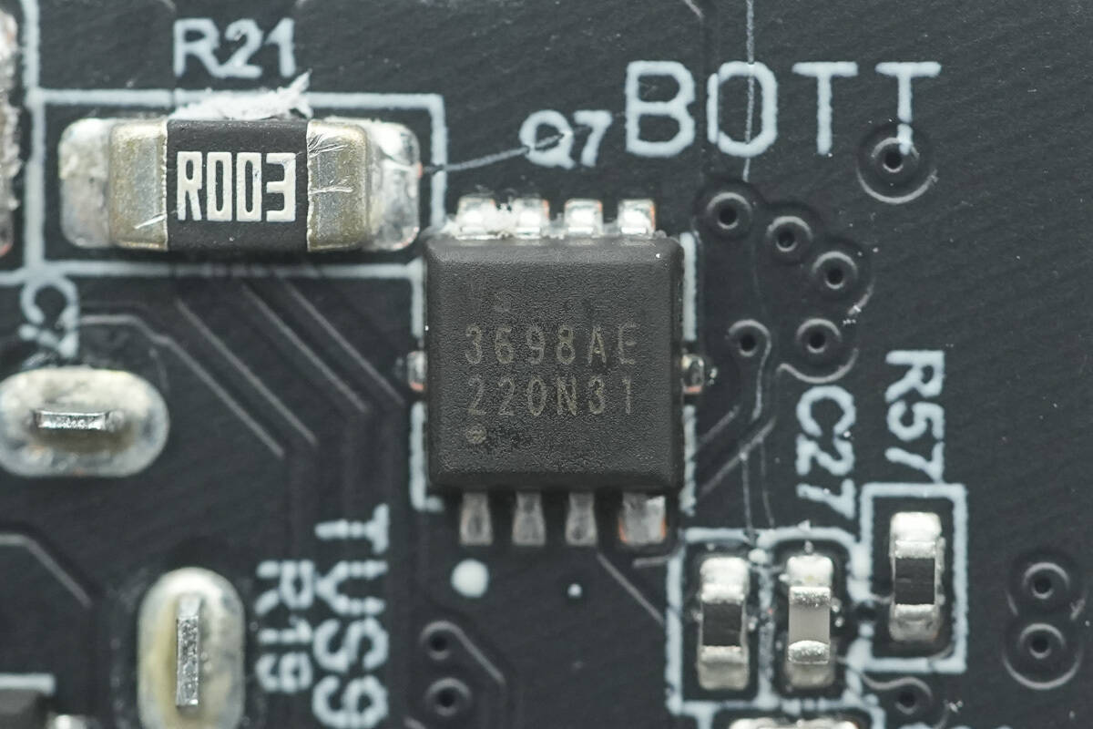
The VBUS MOSFET for the USB-A port also uses the Vergiga VS3698AE.
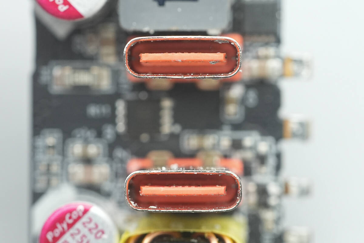
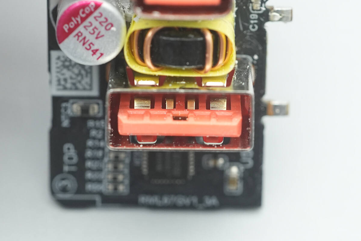
Close-up of the USB-C sockets.
Close-up of the USB-A socket.
Well, those are all components of the Xiaomi 67W GaN Charger.
Summary of ChargerLAB
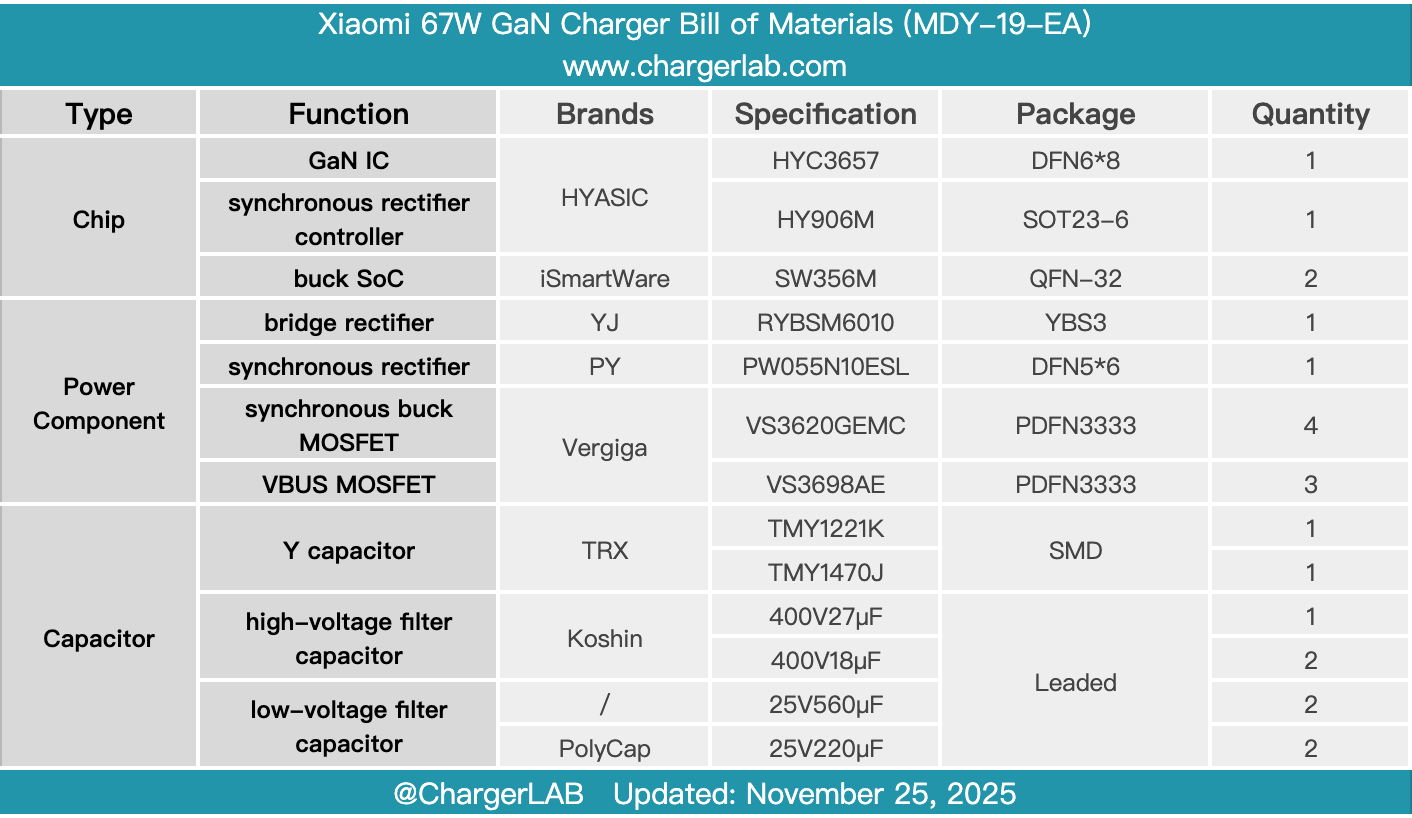
Here is the component list of the Xiaomi 67W GaN Charger for your convenience.
It is equipped with two USB-C ports and one USB-A port. All three ports support 65 W PD and Xiaomi 67 W Surge charging, and are also compatible with QC and PPS. It supports a 45 W + 20 W dual-port fast-charging scheme, meeting the simultaneous fast-charging needs of laptops and smartphones.
After taking it apart, we found that it uses a HYASiC HYC3657 + HYC906M integrated GaN power solution. The outputs are controlled by two iSmartWare SW356M buck protocol chips for the three ports. Capacitors are sourced from Koshin and PolyCap. The module features extensive thermal grease filling and additional heat sinks, with graphite thermal pads applied on the inner side of the housing to assist heat dissipation. Overall, the build quality and materials are reliable.
Related Articles:
1. Teardown of Gospower 3000W Switching Power Supply (G1236-3000WNA)
2. Teardown of CUKTECH 25 Power Bank SE (LPB252N)
3. Teardown of ASUS Adol 140W GaN Quick Charger (AC140-020A)