Introduction
We obtained the original 100W GaN charger for the Xiaomi 17 series. This charger features a customized USB-A port and supports 65W PD fast charging as well as Xiaomi’s proprietary 100W fast-charging protocol. It accepts a wide AC input range of 100–240 V.
The charger offers zero standby power consumption, reducing energy waste and supporting environmental protection. It also uses semi-encapsulated prongs with insulating sleeves to improve safety. Next, let’s take a closer look at its internal components and design.
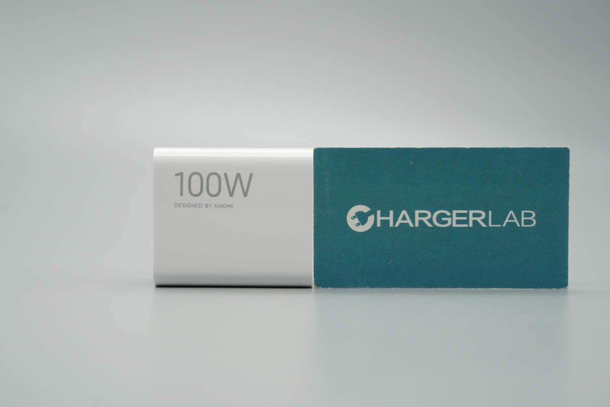
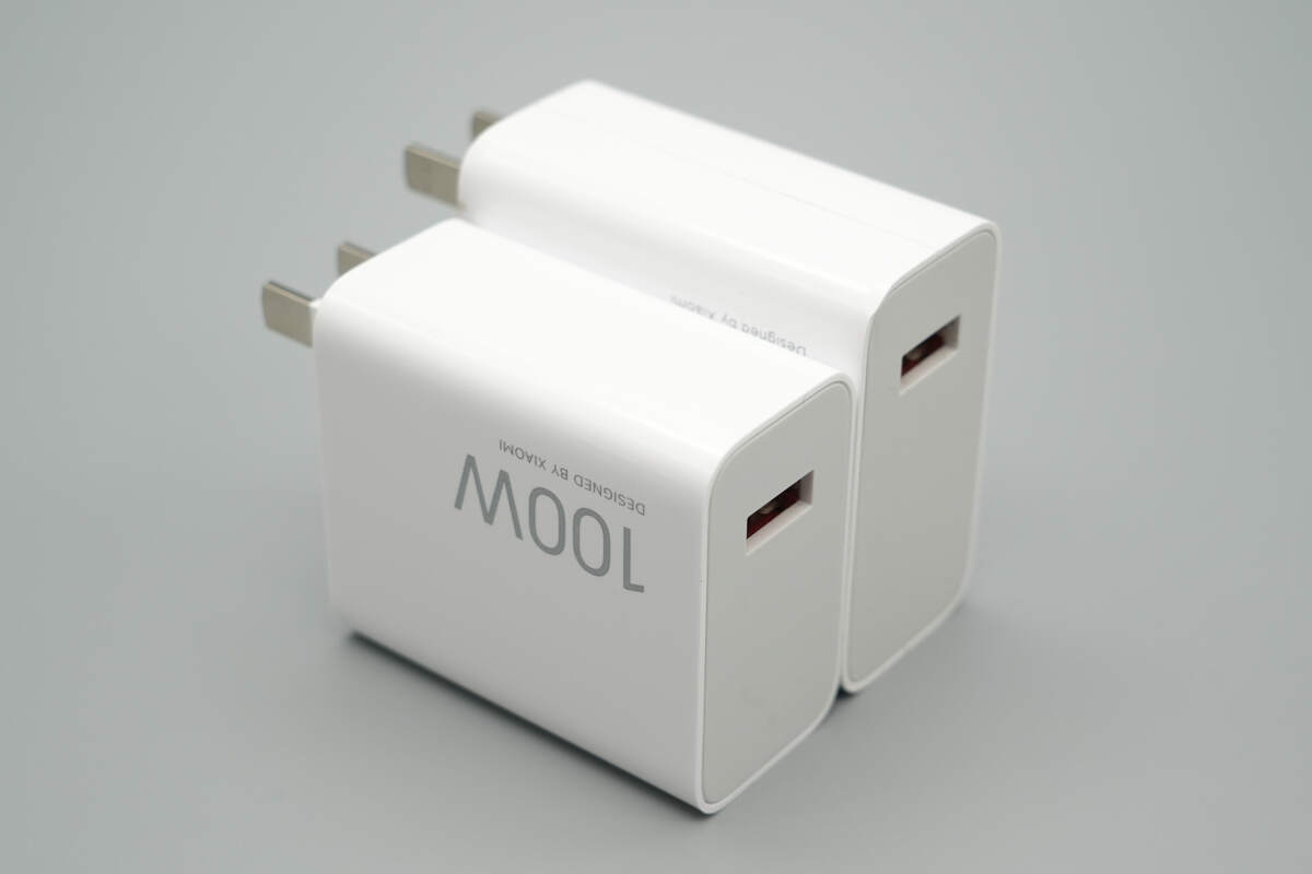
Product Appearance
The outer casing is made of flame-retardant PC material with a glossy finish.
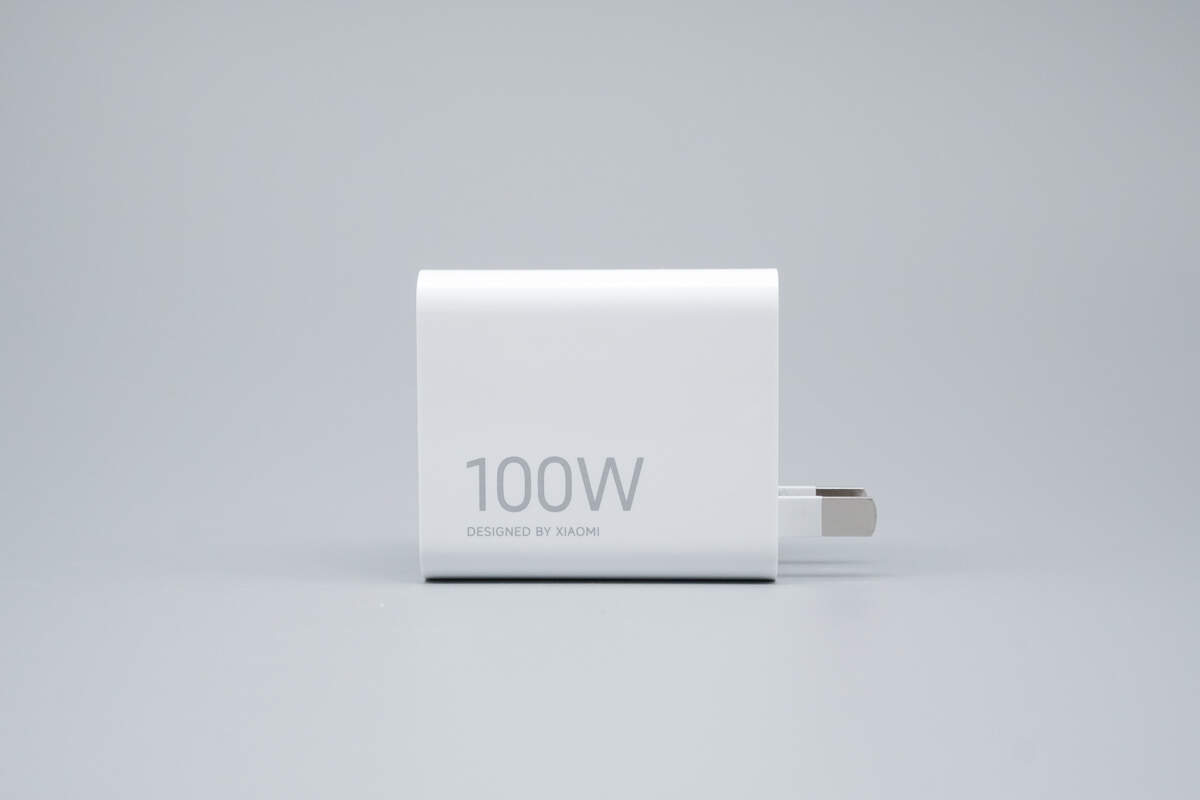
Both sides of the charger body are printed with “100W” and “DESIGNED BY XIAOMI.”
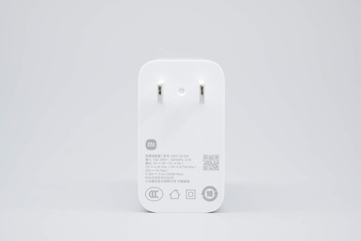
The input-side housing is printed with the charger’s specifications.
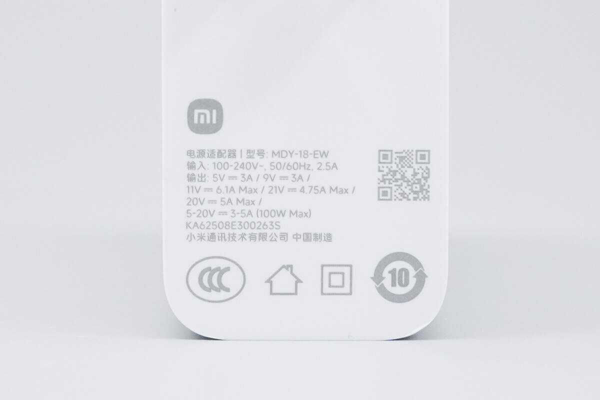
Model: MDY-18-EW
Input: 100–240V~, 50/60 Hz, 2.5A
Output: 5V⎓3A; 9V⎓3A; 11V⎓6.1A Max; 21V⎓4.75A Max; 20V⎓5A Max; 5–20V⎓3–5A (100W Max)
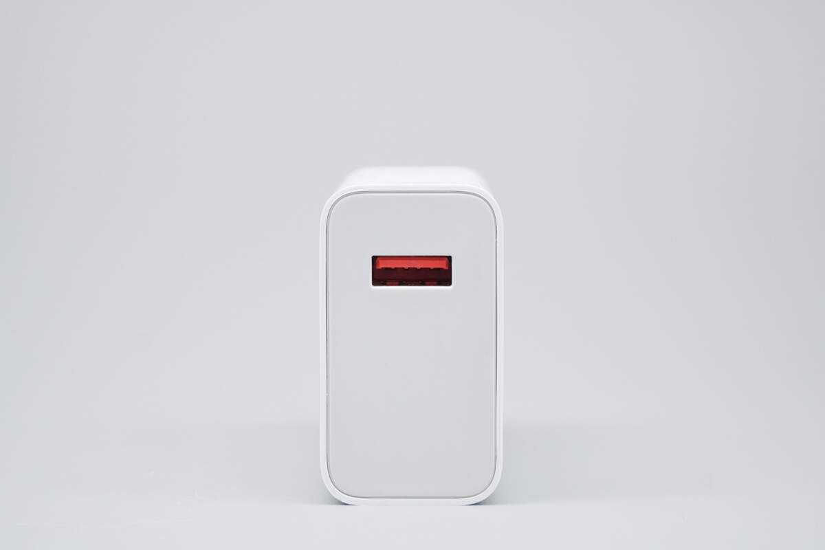
There is a single USB-A output port.
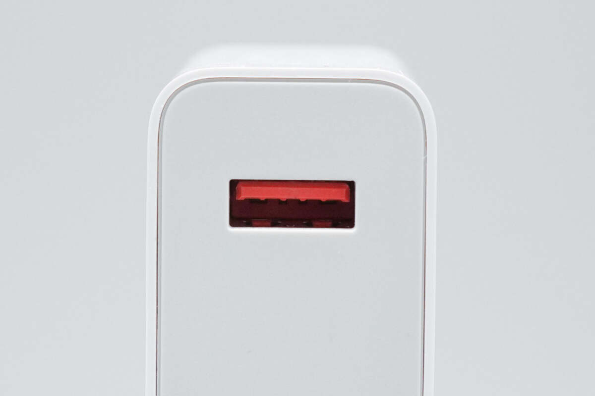
The front end of the plastic sheet contains special pins, which enable support for Xiaomi’s proprietary fast-charging protocol as well as PD fast charging when used with Xiaomi’s dedicated USB-A cable.
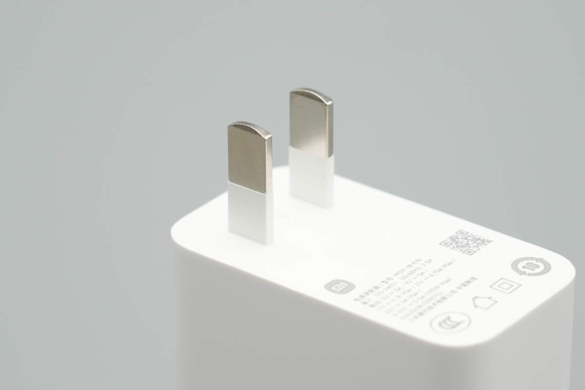
The charger uses semi-encapsulated prongs with insulating sleeves, enhancing safety.

The length of the charger is about 55.8 mm (2.2 inches).
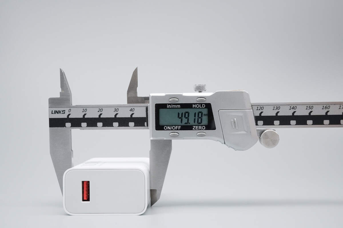
The height is about 49.2 mm (1.94 inches).
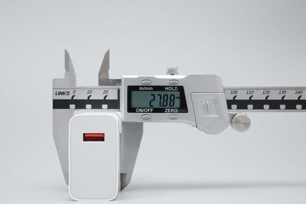
The width is about 27.9 mm (1.098 inches).
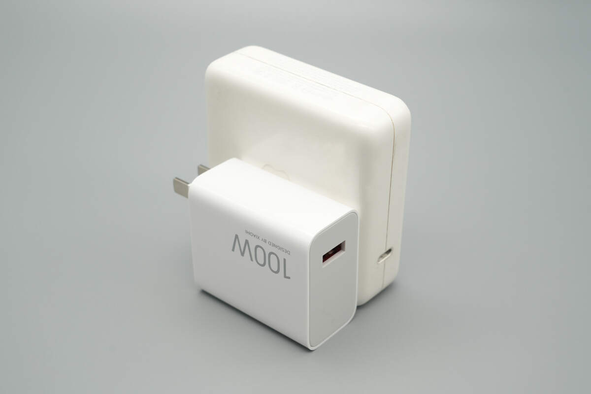
Its size is approximately half that of the Apple 96W charger.
It is slightly smaller than the Xiaomi 120W charger.
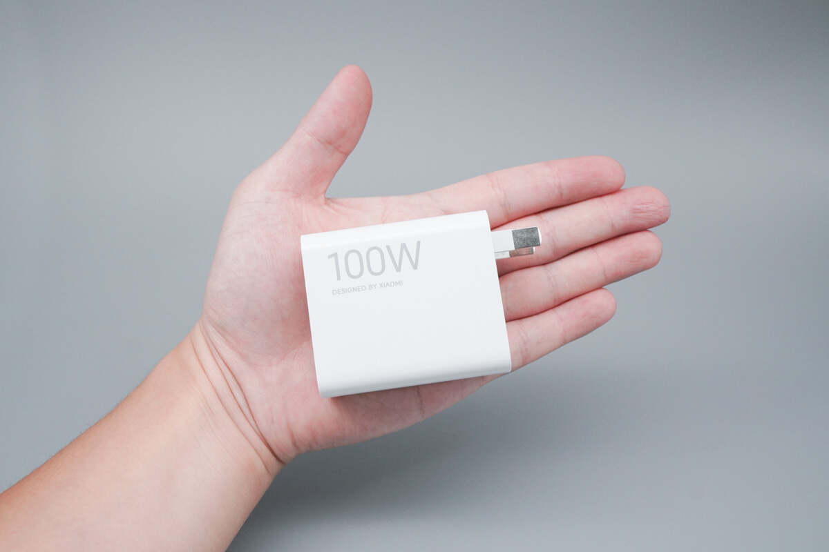
That's how big it is in the hand.
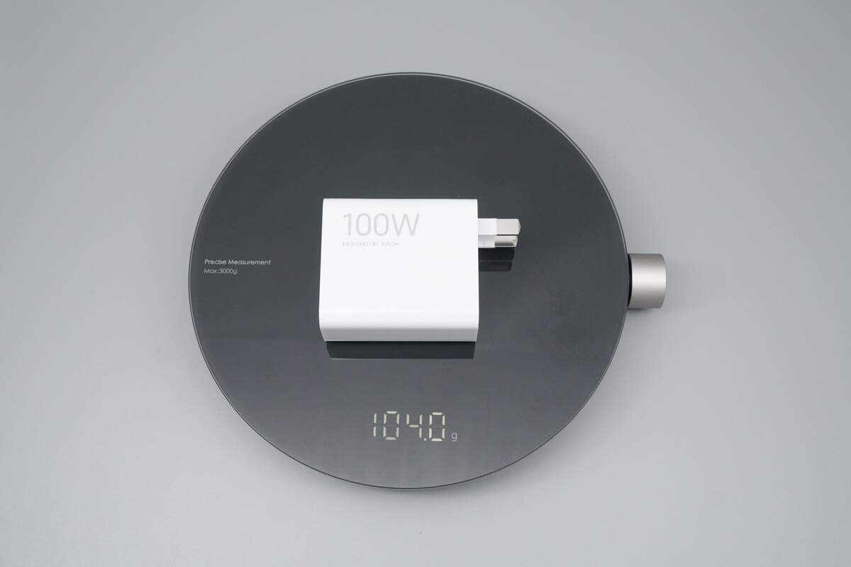
The weight is about 104 g (3.67 oz).
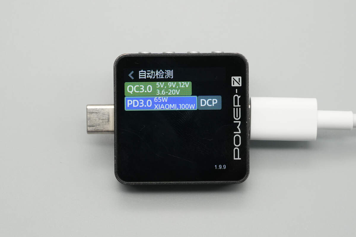
ChargerLAB POWER-Z KM003C shows that it supports QC3.0, PD3.0, DCP charging protocols, as well as Xiaomi’s 100W proprietary fast-charging protocol.
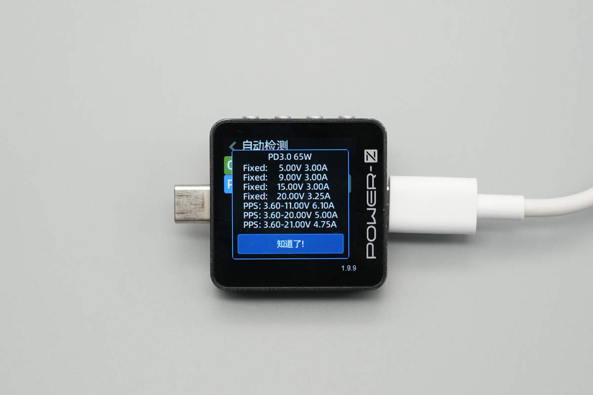
It features four fixed PDOs: 5V 3A, 9V 3A, 15V 3A, and 20V 3.25A, as well as three PPS voltage ranges for Xiaomi: 3.6–11V 6.1A, 3.6–20V 5A, and 3.6–21V 4.75A.
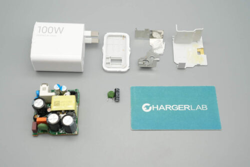
Teardown
Next, let's take it apart to see its internal components and structure.
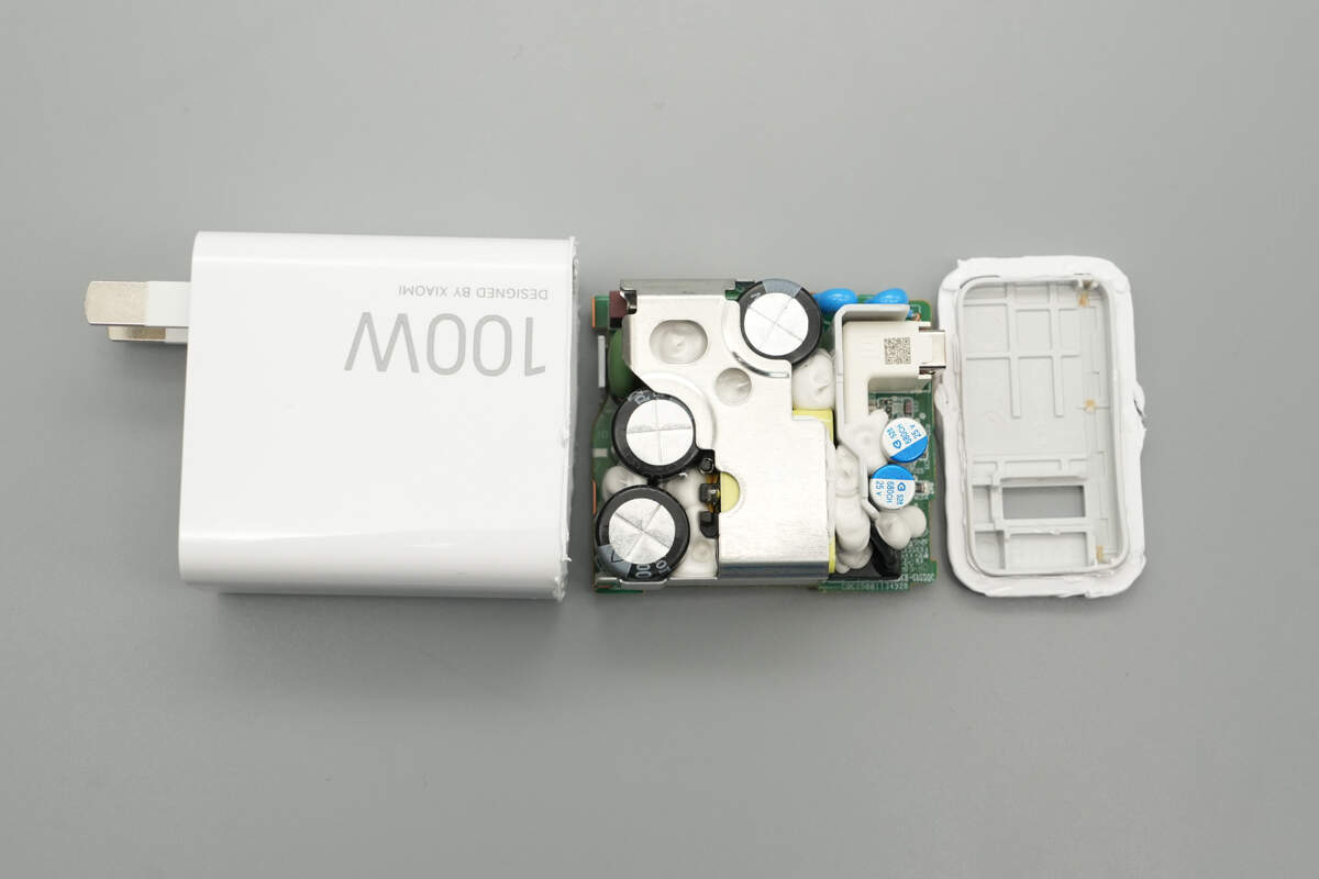
Cut open the casing to remove the PCBA module.
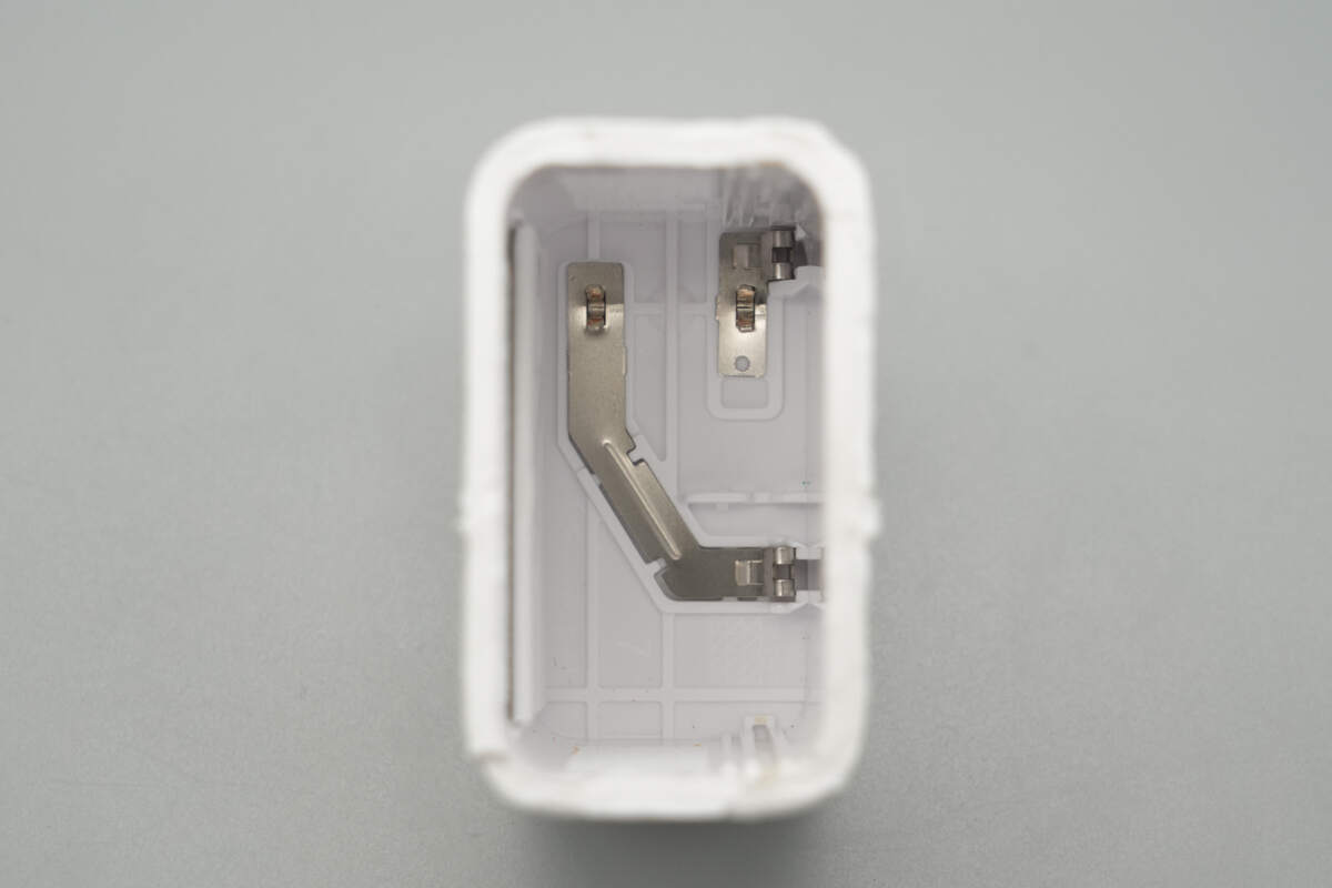
The input side uses metal spring contacts for electrical connection.
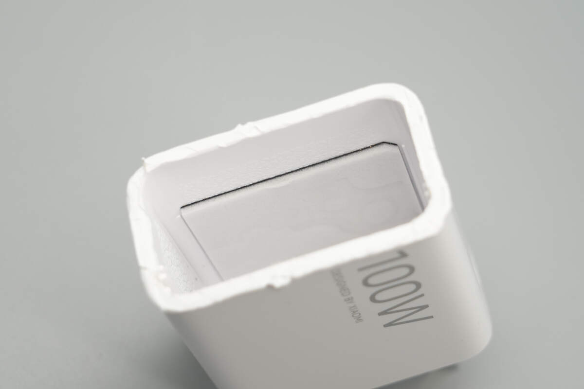
Inside the casing, cushioning foam and a thermal pad are applied.
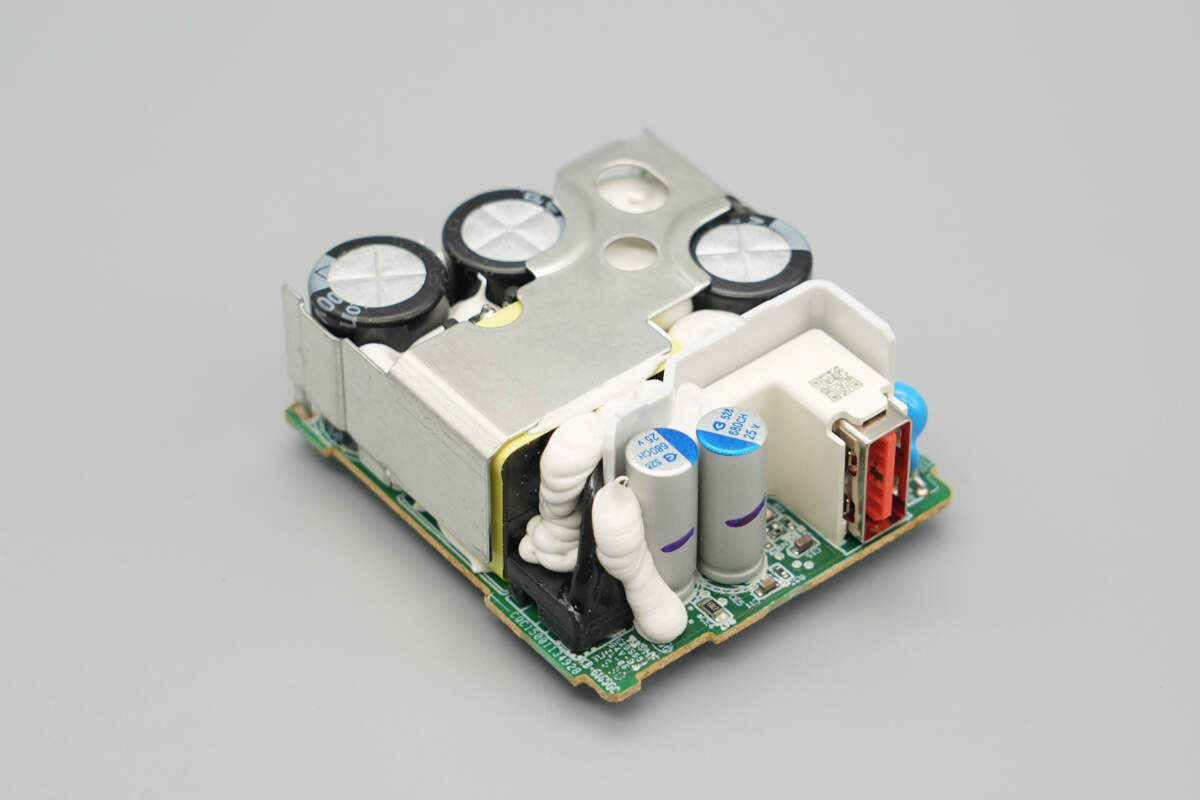
The front side of the PCBA module features a heatsink, and an isolation plate is placed between the transformer and the low-voltage components.
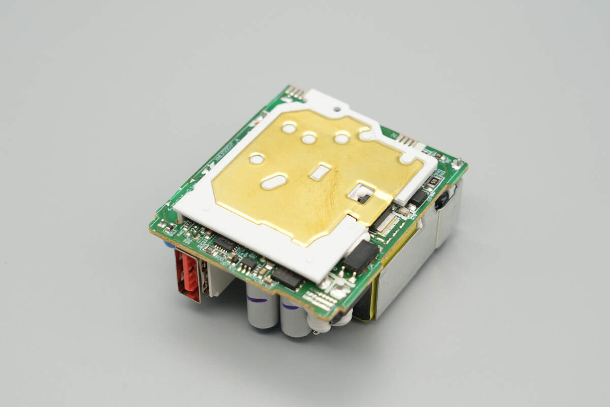
On the back side, there is an isolation plate along with a brass heatsink.
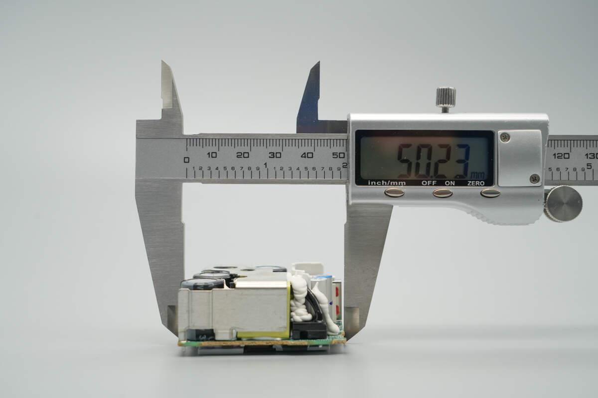
The length of the PCBA module is about 50.2 mm (1.98 inches).
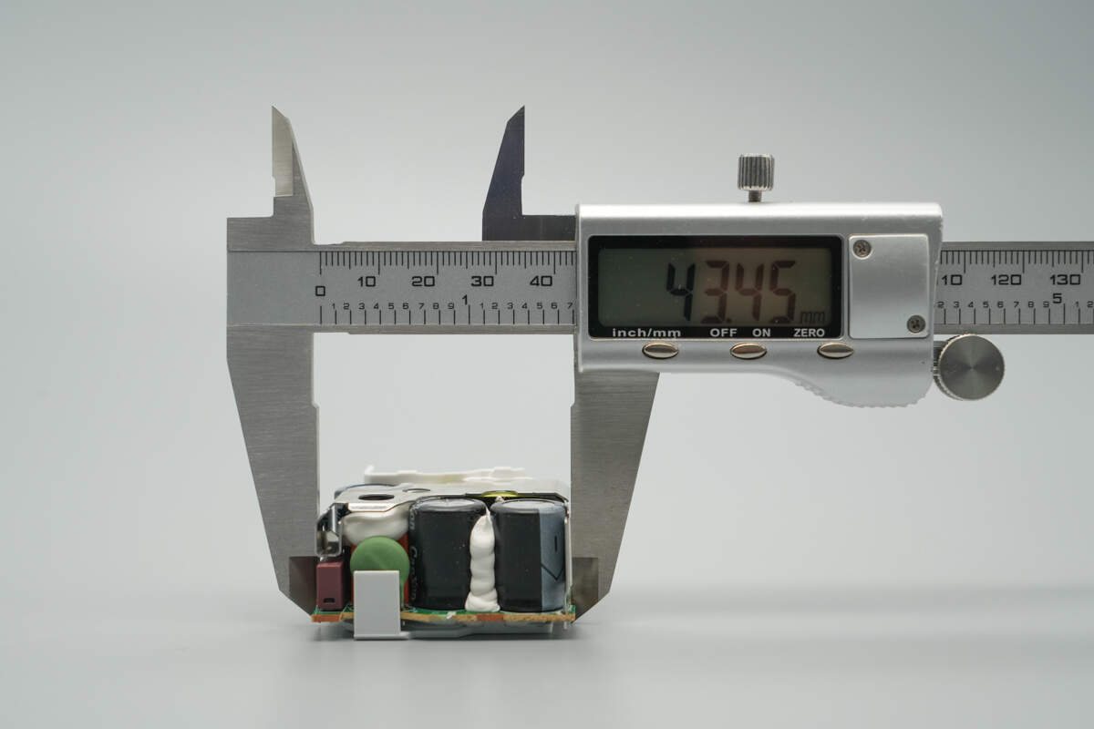
The width is about 43.5 mm (1.71 inches).
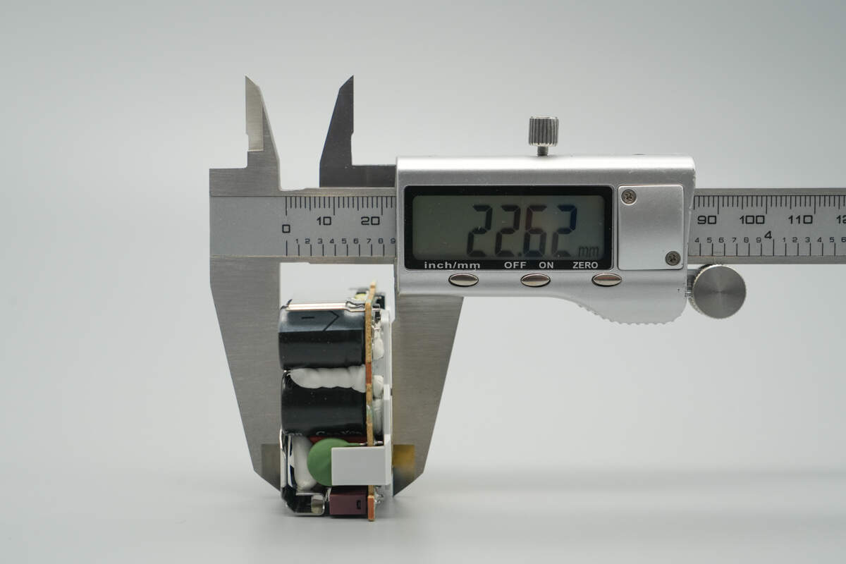
The thickness is about 22.6 mm (0.89 inches).
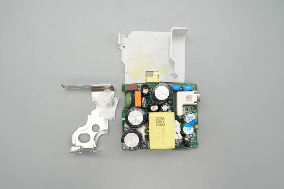
Remove the heatsinks on both the front and back of the module.
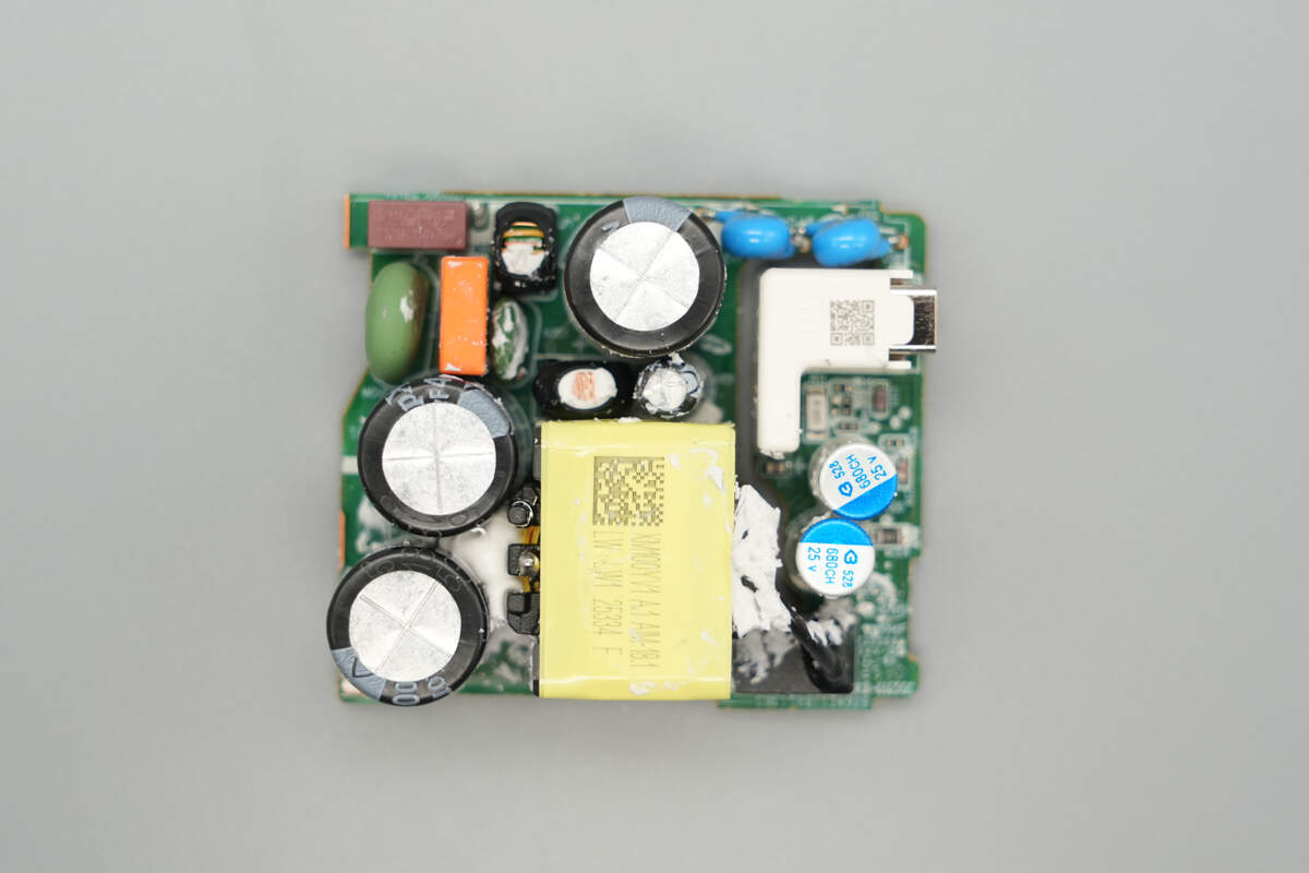
The front side of the PCBA module contains a fuse, varistor, safety X2 capacitor, common mode choke, thermistor, capacitors, filter inductor, transformer, and blue Y capacitors.
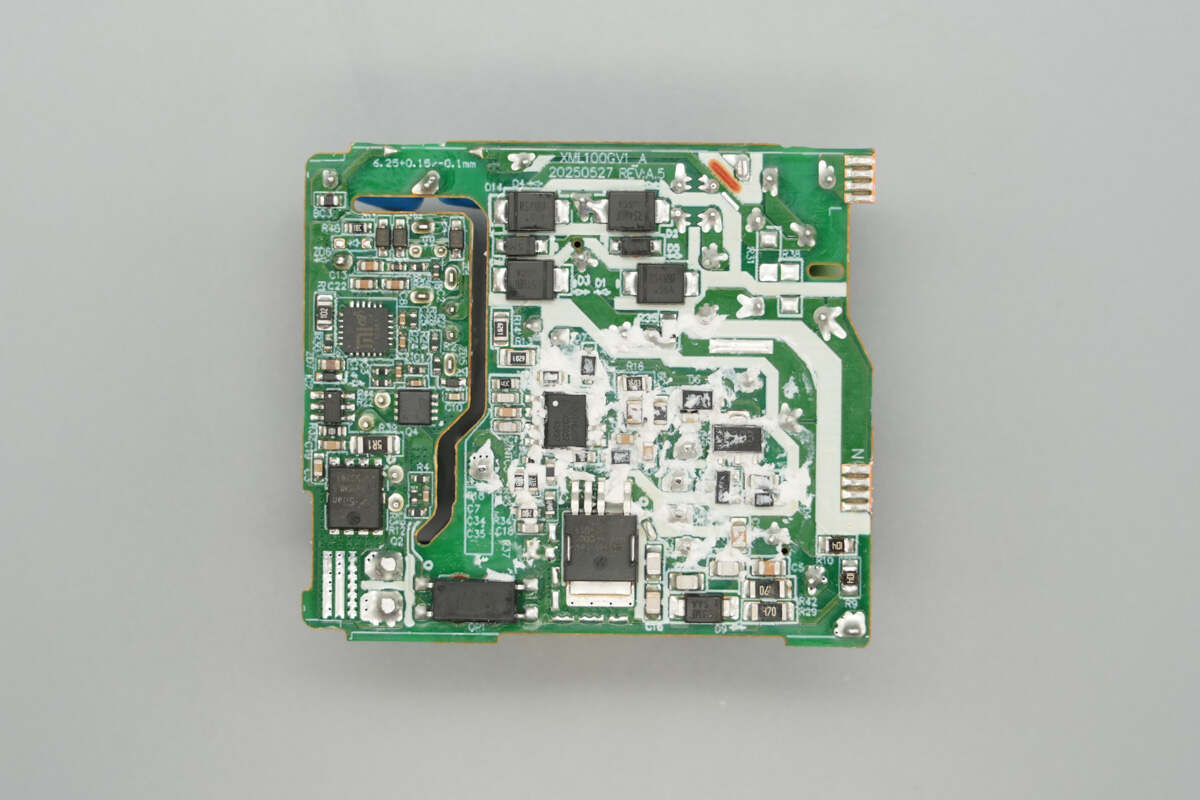
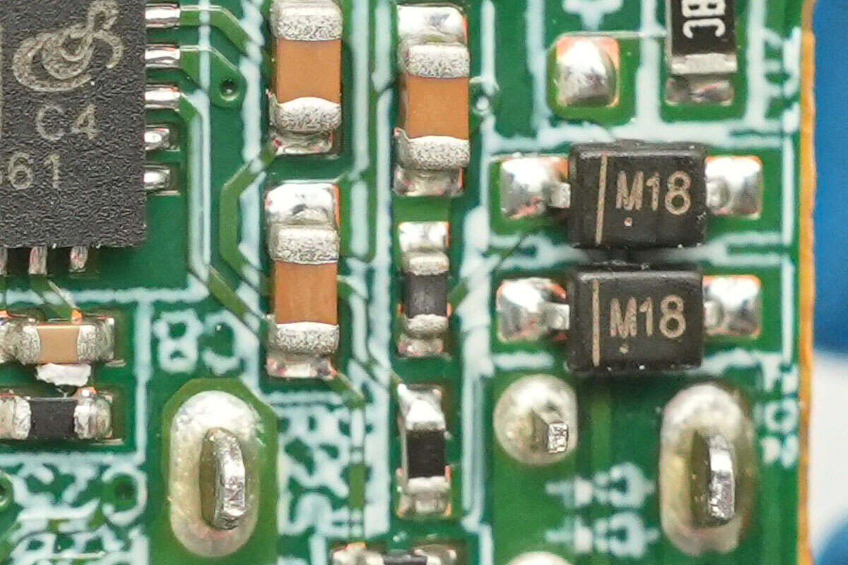
On the back side, there are four rectifiers, the primary control IC, a synchronous rectifier controller, a synchronous rectifier, a protocol chip, and a VBUS MOSFET.
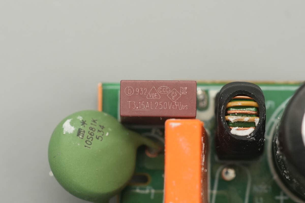
The input fuse is from Betterfuse, part number 932, rated at 3.15 A, 250 V.
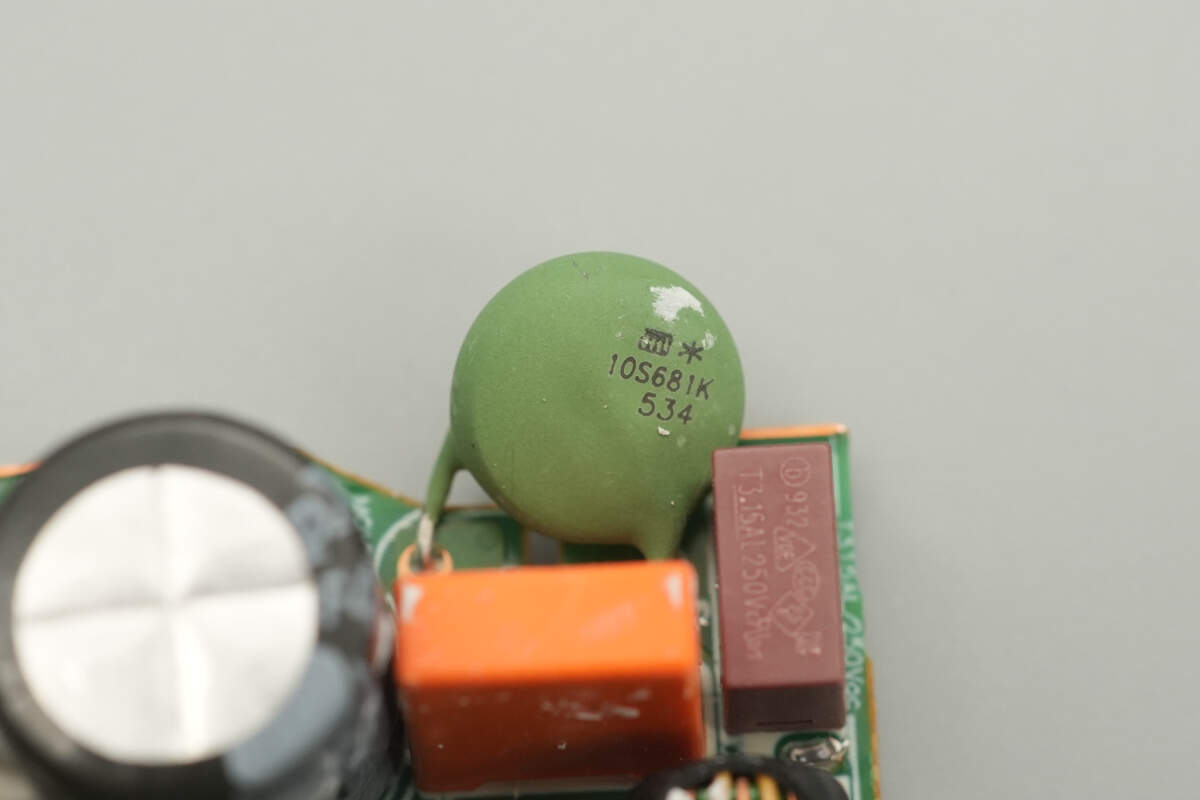
The varistor is from JOYIN, model 10S681K, used to absorb overvoltage surges.
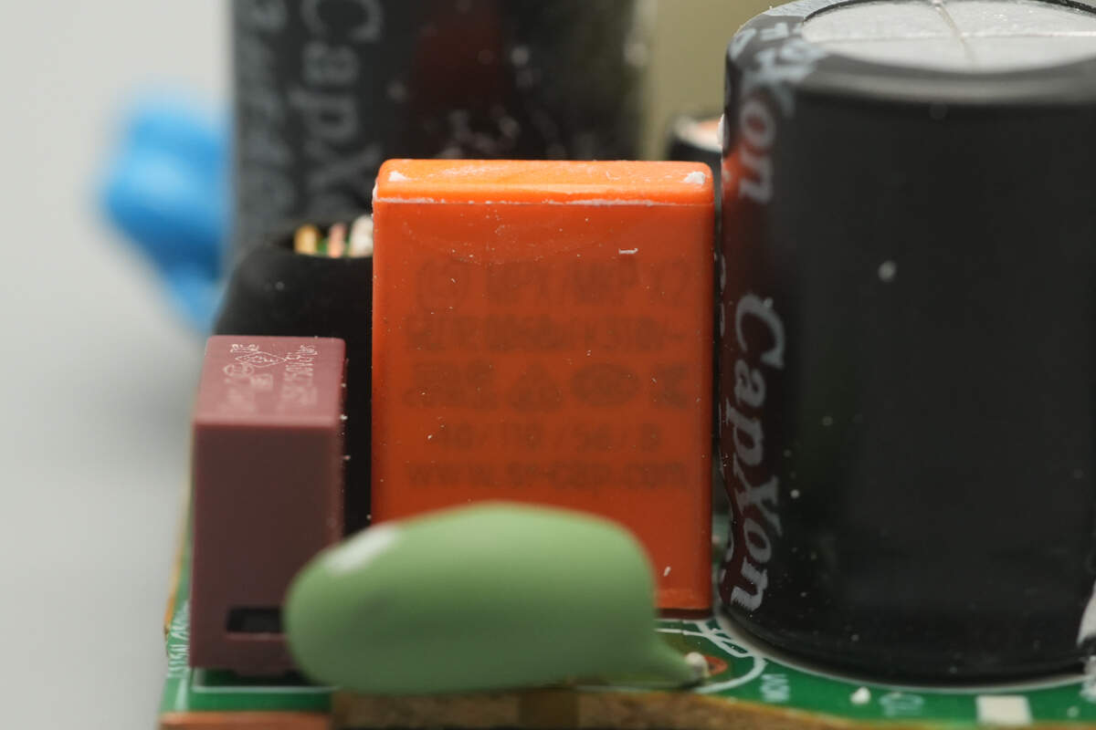
The safety X2 capacitor is from Surong, with a rating of 0.068 μF.
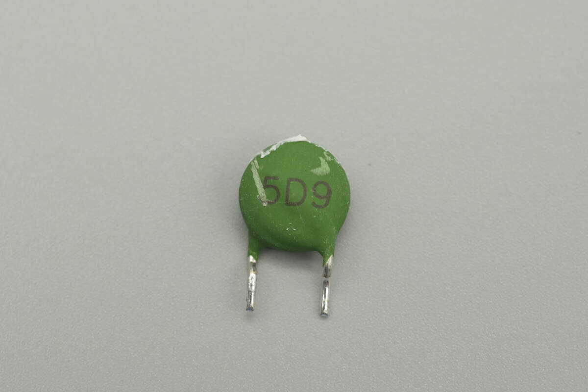
The NTC thermistor marked “5D9” is used to suppress inrush current at power-on.
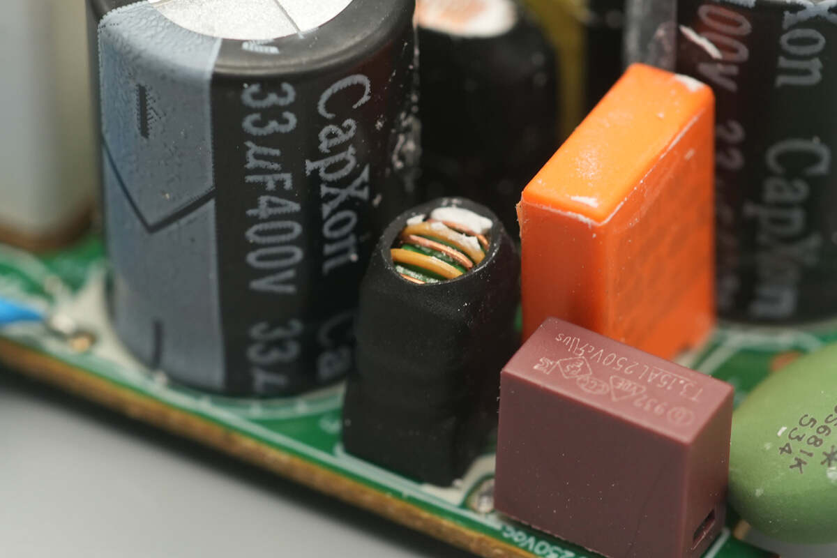
The common mode choke is wound with enameled and insulated wires, features an insulating support at the base, and is sleeved with heat-shrink tubing for insulation.
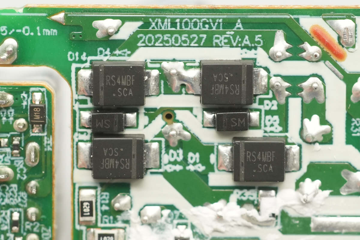
The bridge rectifier is composed of four RS4MBF SMD diodes.
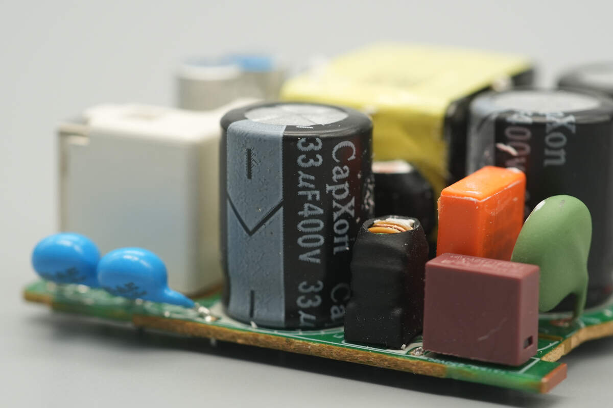
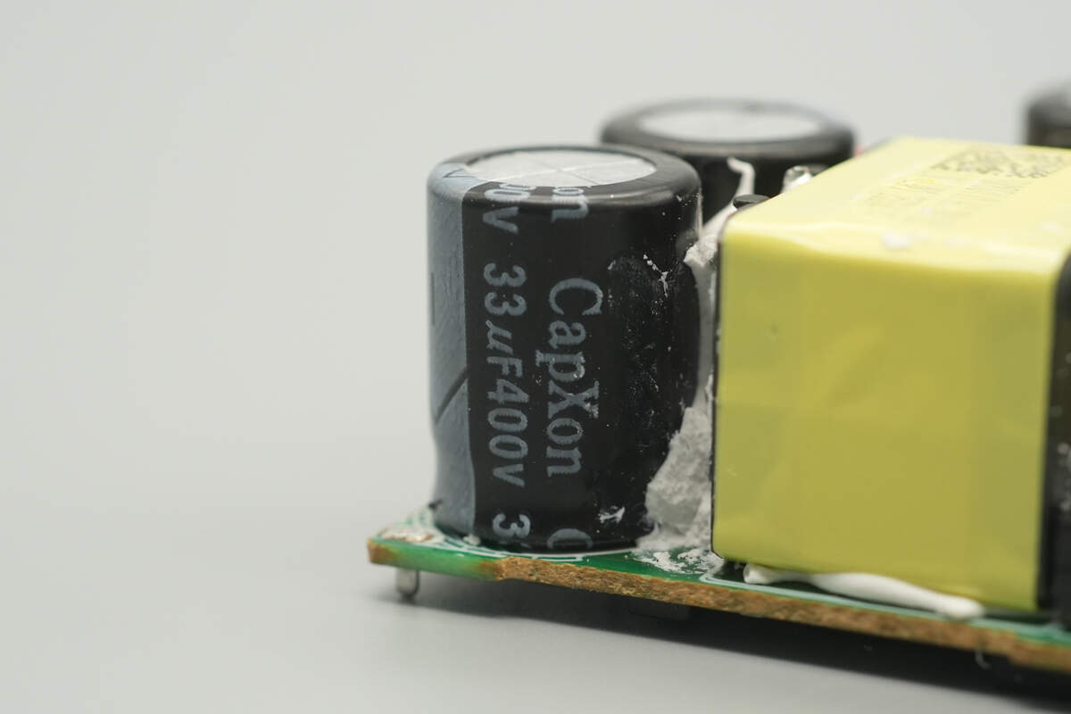
The high-voltage filter capacitor is from CapXon, rated at 33 μF, 400 V.
The differential mode choke is wound with enameled wire and insulated with heat-shrink tubing.
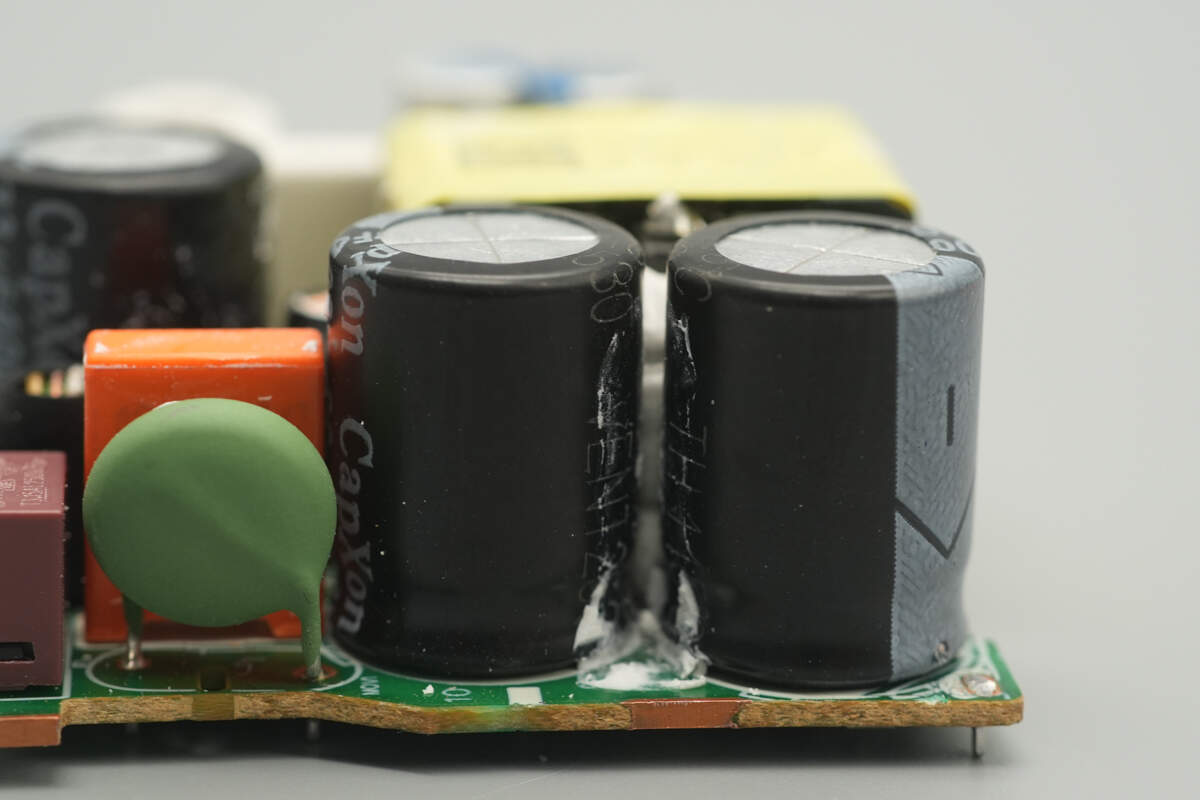
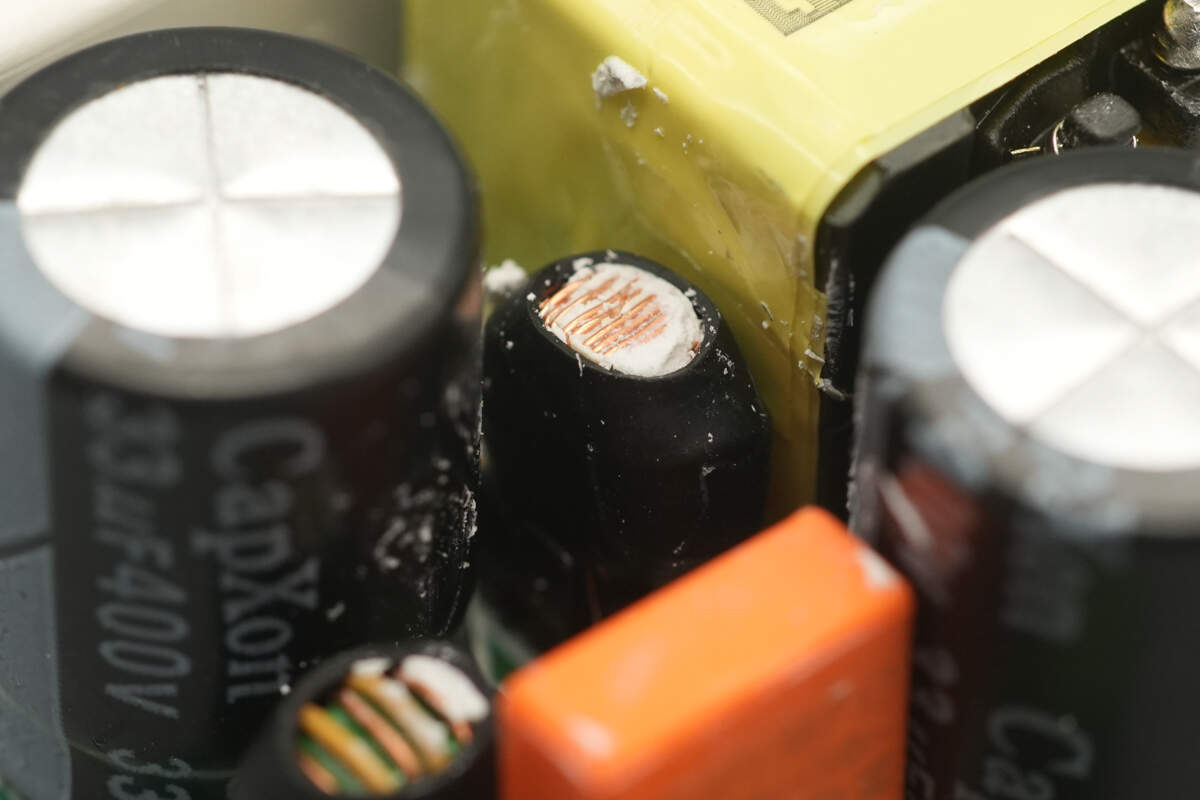
On the other side, there are also two high-voltage filter capacitors.
The filter capacitors have the same rating of 33μF, 400V.
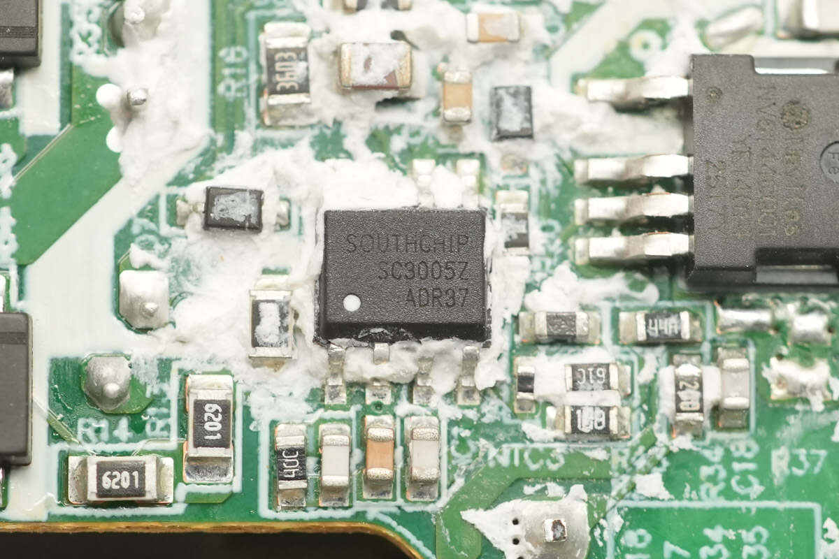
The primary control IC is the SouthChip SC3005Z, a high-performance multi-mode flyback PWM controller supporting CCM, QR, and DCM operating modes. It features built-in X-capacitor discharge and high-voltage startup, enabling ultra-low standby power consumption and extremely fast startup times.
The SC3005Z incorporates adaptive switching frequency foldback, achieving higher efficiency across the entire load range. Under heavy and full loads, it operates at maximum switching frequency, while under light loads, the frequency is automatically reduced, and in discontinuous mode, valley-switching is used for high efficiency. When no device is connected, the protocol chip can put the SC3005Z into a sleep state, allowing the charger to achieve near-zero standby power.
It integrates adaptive overcurrent protection to control the maximum output current on the primary side, making it suitable for USB-PD fast charging and reducing current stress on synchronous rectifiers under extreme conditions. The IC provides comprehensive protection functions, frequency dithering, and intelligent drive to improve EMI performance, and comes in an SOP-7 package.
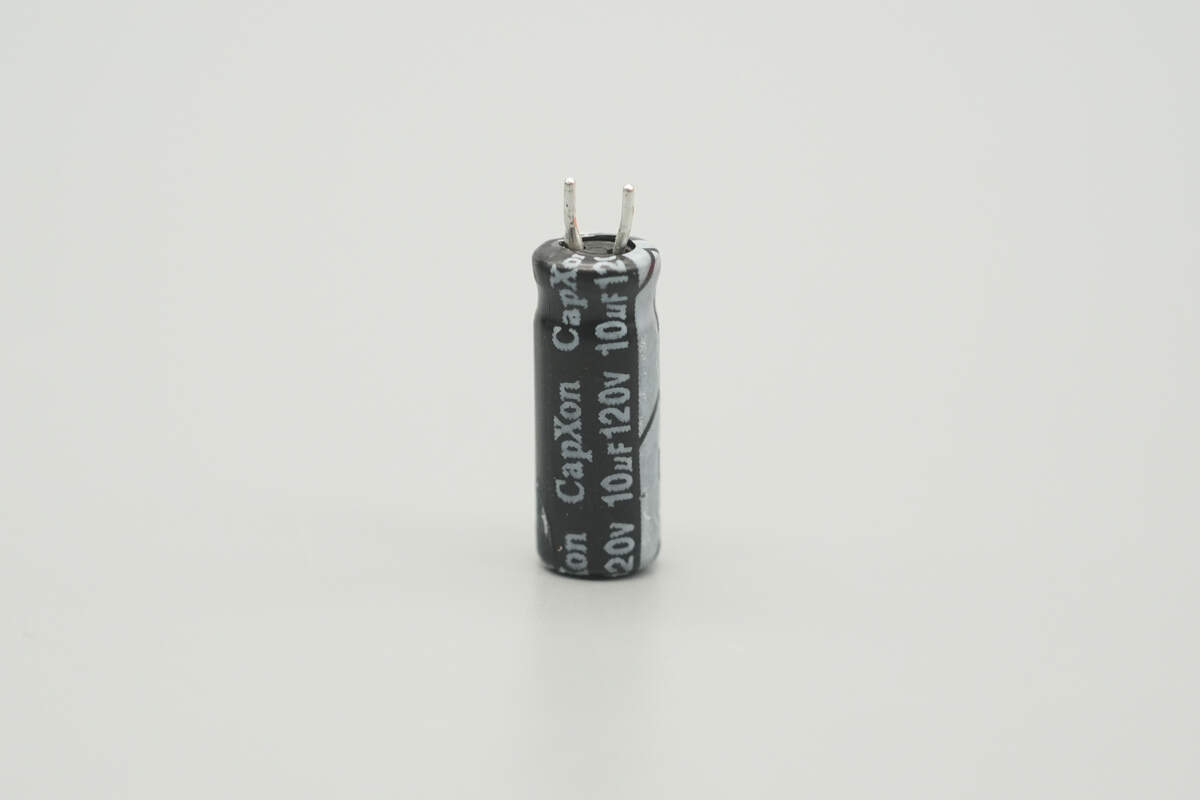
The filter capacitor is from CapXon, rated at 10μF, 120V.
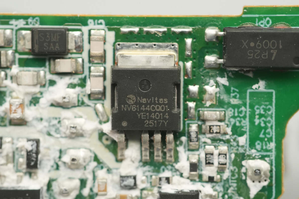
The GaN power chip is from Navitas, model NV6144C. It integrates a high-performance enhanced GaN FET with a voltage rating of 700 V and an on-resistance of 260 mΩ. It supports 3.3 V, 5 V, and 15 V PWM logic input, features programmable high-precision current sensing, and includes overtemperature protection. The chip operates over a wide supply voltage range of 10–24 V, offers ultra-low standby and sleep power consumption, and comes in a DPAK-4L package.
The transformer core is insulated with winding tape.
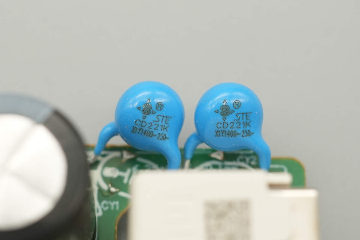
The blue Y capacitors are from STE, with two units connected in series to enhance safety.
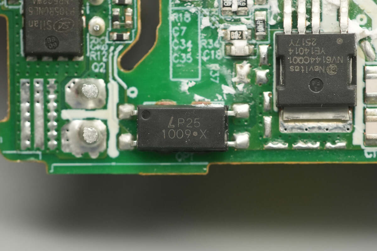
The optocoupler is from LITEON, model LTV-1009, used for output voltage feedback regulation.
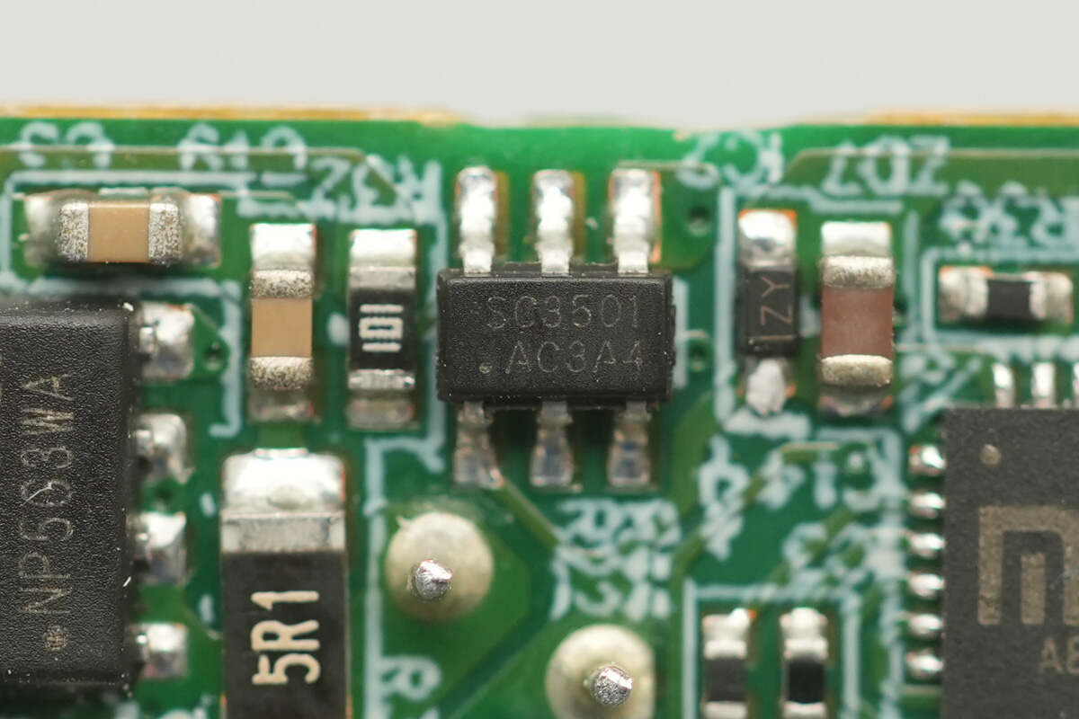
The synchronous rectifier controller is from SouthChip, model SC3501. It supports adaptive turn-on detection and fast turn-off without requiring an auxiliary winding for power. The output voltage can reach up to 22 V and drop as low as 0 V, making it suitable for PD fast-charging applications. Its patented adaptive turn-on detection circuit prevents false triggering of the synchronous rectifier and is compatible with various MOSFETs. It features ultra-low quiescent current, supports multiple operating modes, and allows both high-side and low-side synchronous rectification. The controller uses very few external components and comes in an SOT23-6 package.
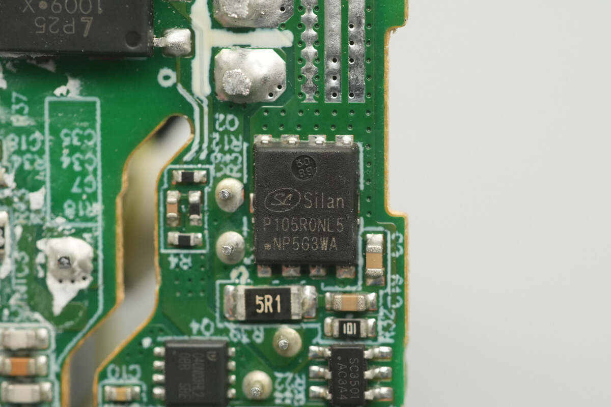
The synchronous rectifier is from Silan, marked P105R0NL5, model SVGP105R0NAL5. It is an NMOS with a voltage rating of 100 V, an on-resistance of 3.8 mΩ, and comes in a PDFN 5×6 package.
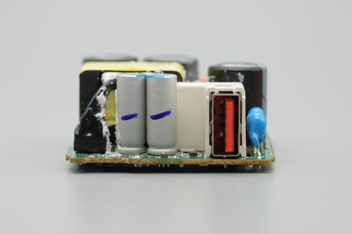
The output side is equipped with solid capacitors and a USB-A socket.
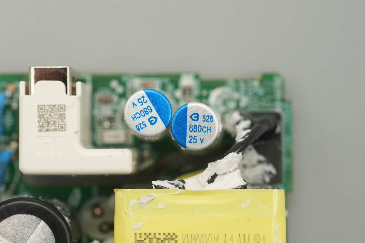
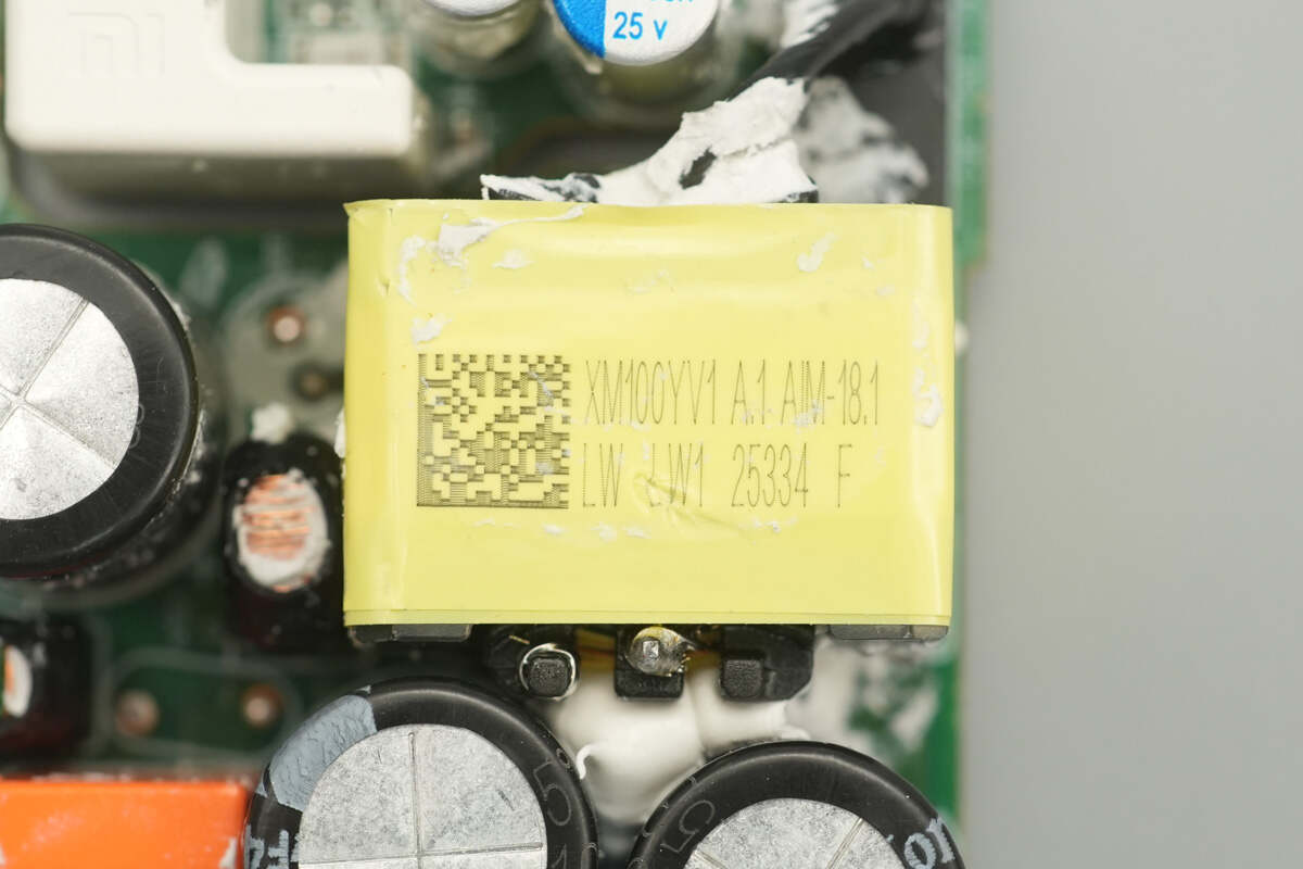
The solid capacitors are from BERYL, rated at 680μF, 25V, with two units connected in parallel.
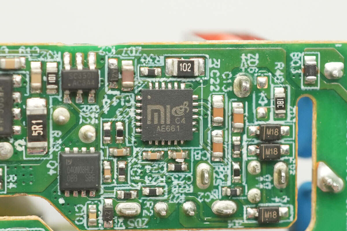
The protocol chip is a Xiaomi-customized model from SouthChip, marked with both the Xiaomi and SouthChip logos, and labeled “C4.” It integrates a 32-bit high-performance MCU that supports zero-standby power functionality.
The chip includes an internal LDO, a VBUS MOSFET driver, and VBUS discharge circuitry. It features a built-in 10-bit ADC for voltage, current, and other parameter measurements, and supports line-loss compensation. Internal temperature monitoring is included, with the option to connect an external NTC for ambient temperature detection. It also supports I²C communication and optocoupler feedback, as well as AC voltage and load detection. The package type is QFN-24.
An NTC thermistor is located on the right side of the protocol chip to monitor the internal temperature of the charger and provide overtemperature protection.
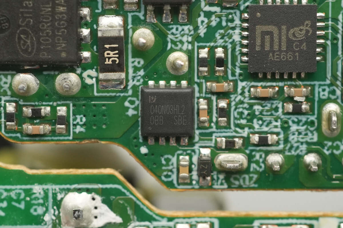
The output VBUS MOSFET is from Pingwei, marked 040N03HL2, and comes in a DFN 3×3 package.
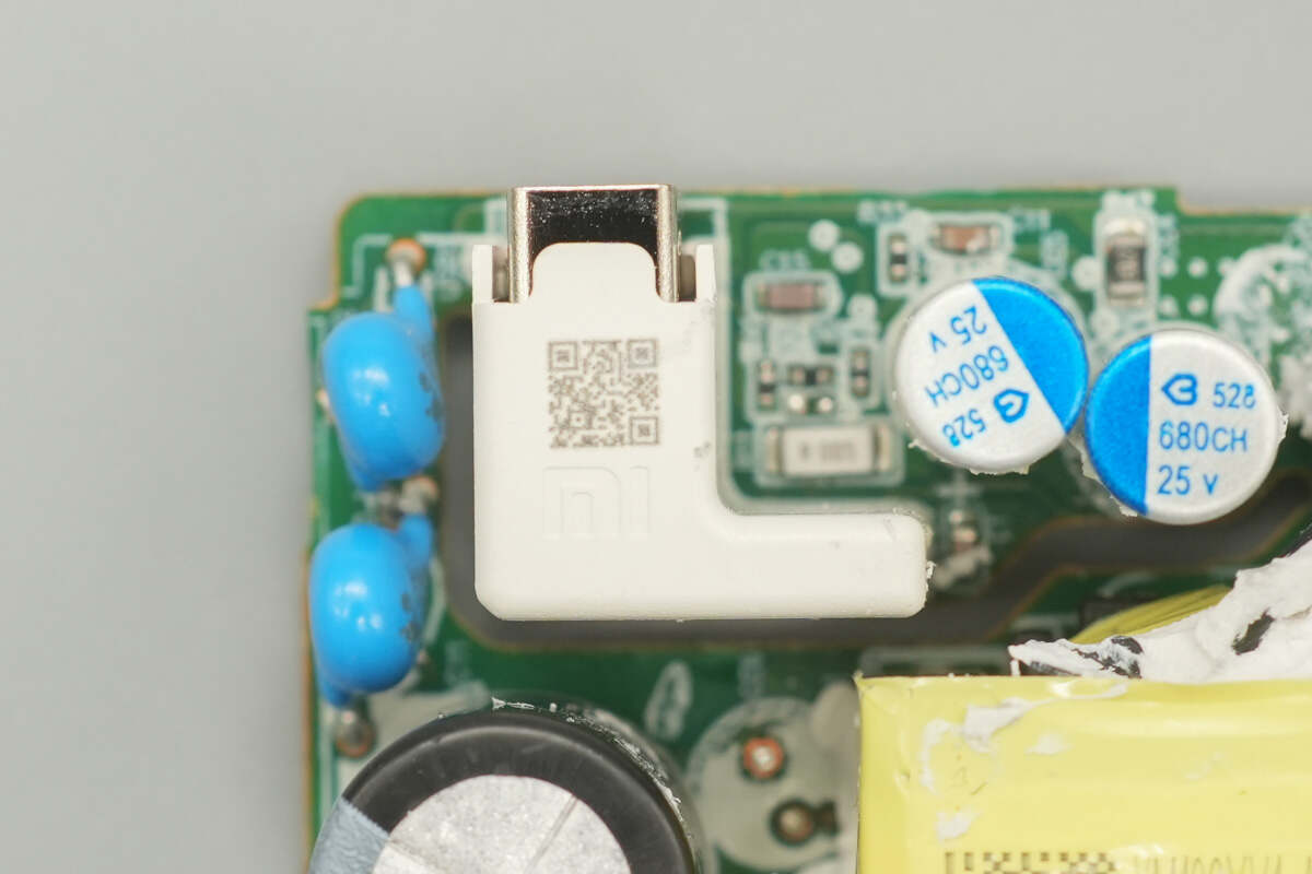
The USB-A socket is insulated with a plastic housing.
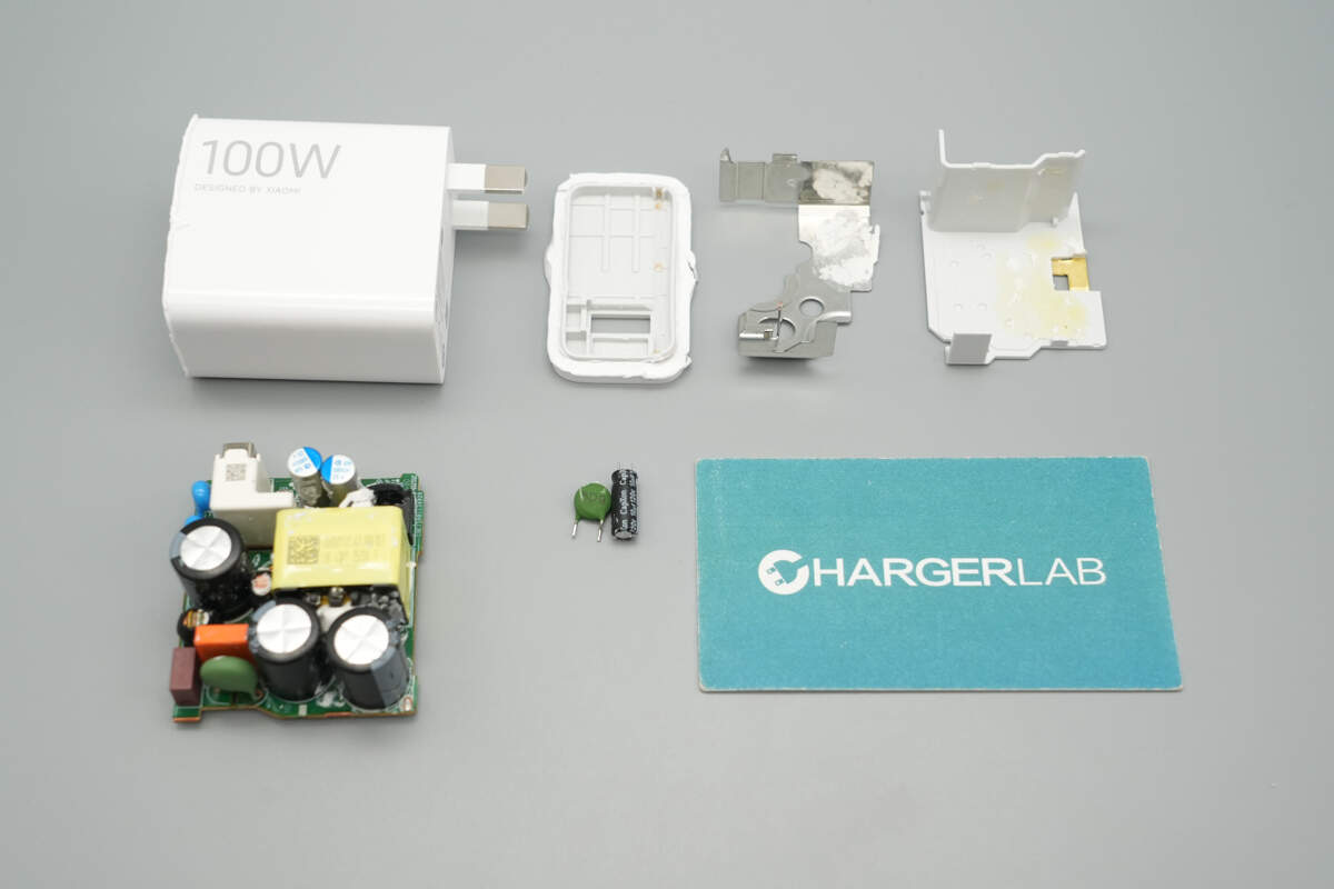
Well, those are all components of the Xiaomi 100W GaN Charger for Xiaomi 17 Series.
Summary of ChargerLAB
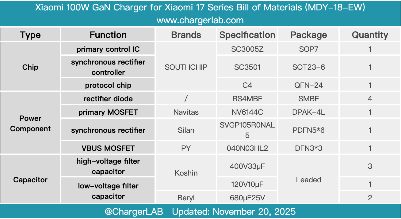
Here is the component list of the Xiaomi 100W GaN Charger for Xiaomi 17 Series for your convenience.
It supports a wide input voltage range of 100–240 V and provides Xiaomi’s 100W proprietary fast charging as well as 65W PD, meeting the charging needs of smartphones, tablets, and laptops. It also features zero standby power, improving energy efficiency when idle and effectively protecting the environment.
After taking it apart, we found that it uses a SouthChip solution, featuring the SC3005Z primary control IC paired with an SC3501 synchronous rectifier controller, and a protocol chip marked “C4.” The primary MOSFET is a Navitas NV6144C, paired with a Silan synchronous rectifier.
The high-voltage filter capacitors are from CapXon, and the solid capacitors are from BERYL. Thanks to SouthChip’s complete fast-charging solution, the primary and secondary chips work together efficiently, allowing the charger to achieve ultra-low power consumption in standby mode, meeting the design requirement for zero standby power.
Related Articles:
1. Teardown of Belkin BoostCharge Pro 140W 4-Port GaN Wall Charger (WCH014)
2. Teardown of SMSL GaN Power Amplifier (PA200)
3. Teardown of RedMagic 80W Air-Cooled Wireless Charging Dock (PA0404)