Introduction
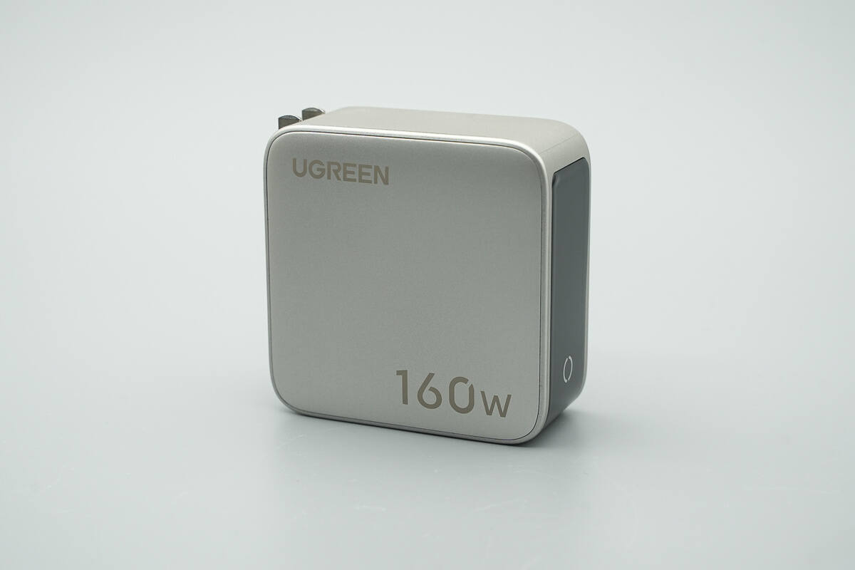
This teardown features UGREEN’s newly released 160W multi-port GaN charger. The charger is equipped with four USB-C ports and one USB-A port, offering a total output power of 160W. Among them, USB-C1 and USB-C2 support PD 3.1 with up to 140W output, USB-C3 and USB-C4 support up to 30W, and the USB-A port supports up to 22.5W. The device also supports intelligent power distribution across the ports.
An LCD screen on one side of the body displays the total output power and individual power allocation, as well as charging protocols. A touch button allows users to rotate the display orientation and switch between different data views, including temperature monitoring. Next, let’s take a closer look at its internal components and design.
Product Appearance
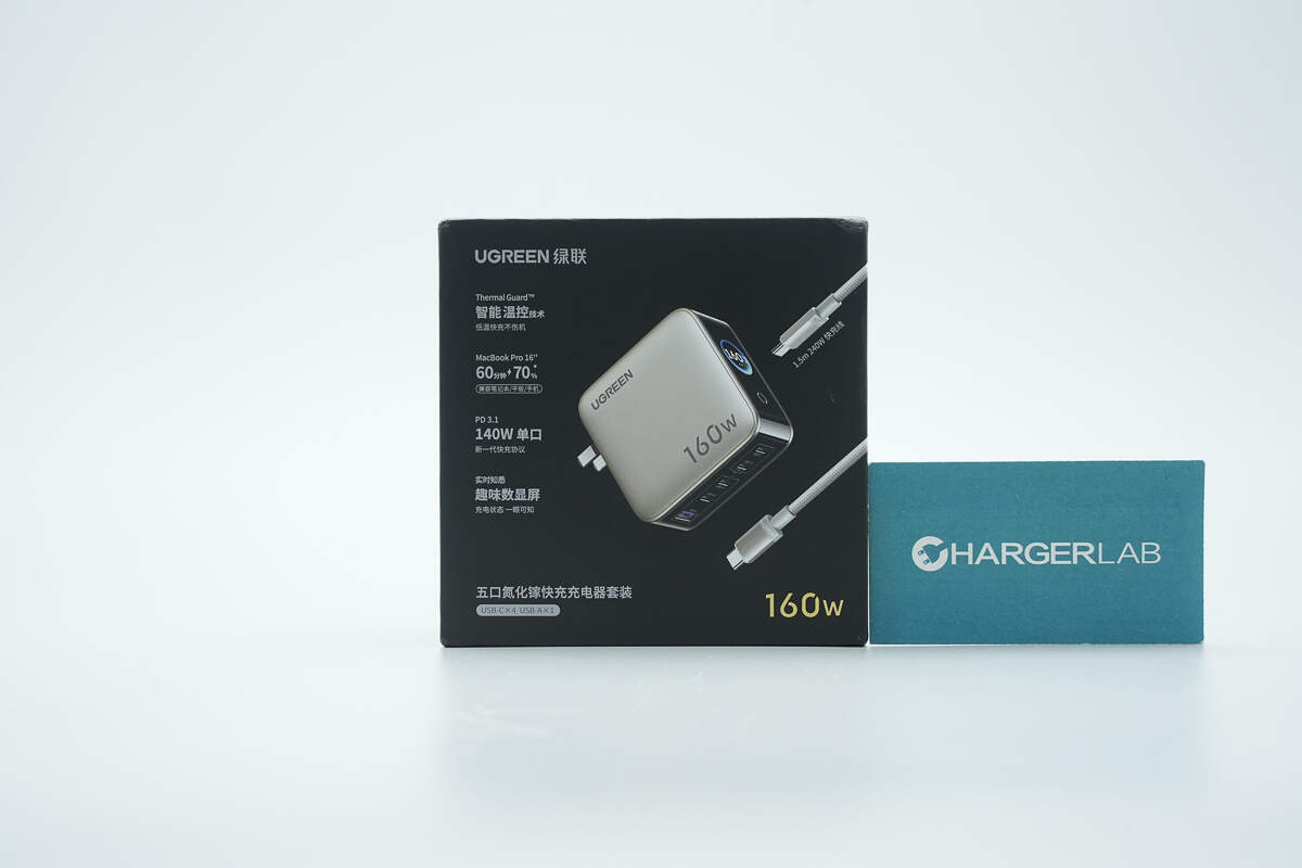
The front of the packaging box features the UGREEN logo, an image of the product, and its key selling points.
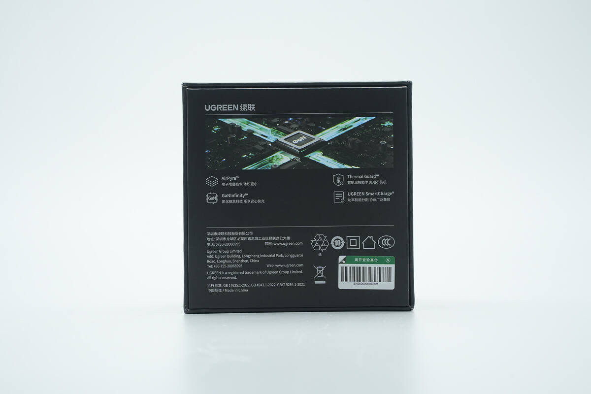
The back of the packaging box lists the product specifications, safety information, and other relevant notes.
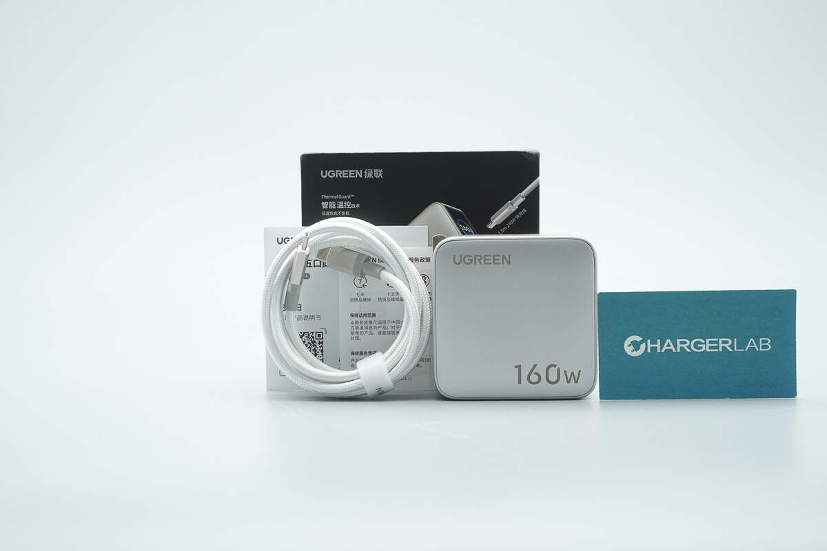
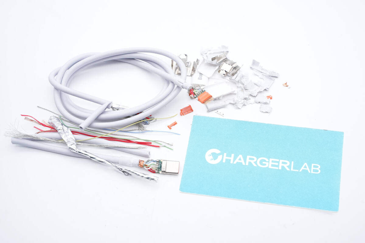
Inside the packaging are the charger itself, a braided charging cable, and a user manual.
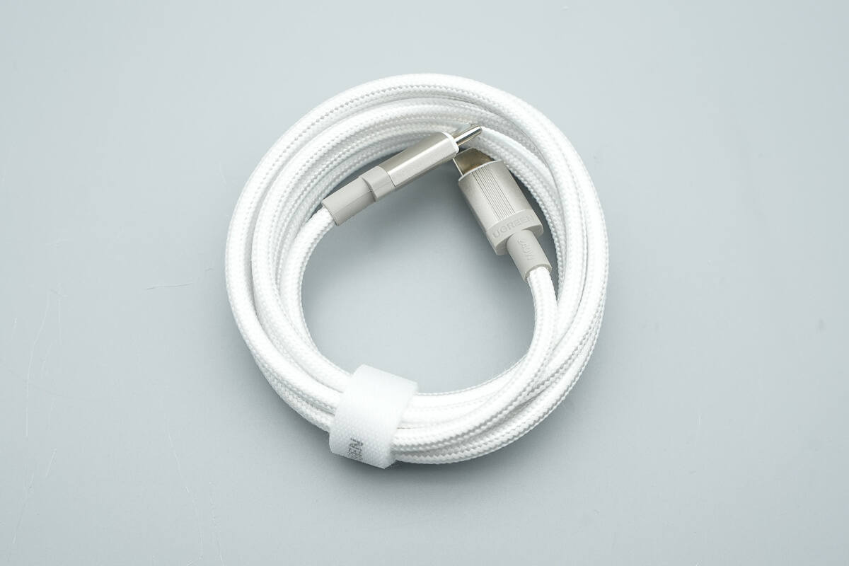
The included charging cable is a dual USB-C type and features a white braided exterior.
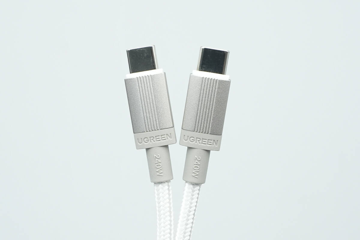
The plug features an aluminum alloy casing with the UGREEN logo and “240W” printed on it.
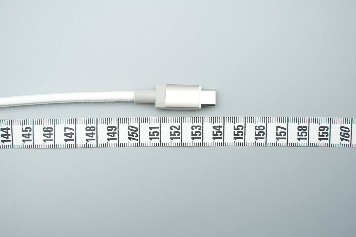
The length of the cable is about 154 cm (60.63 inches).
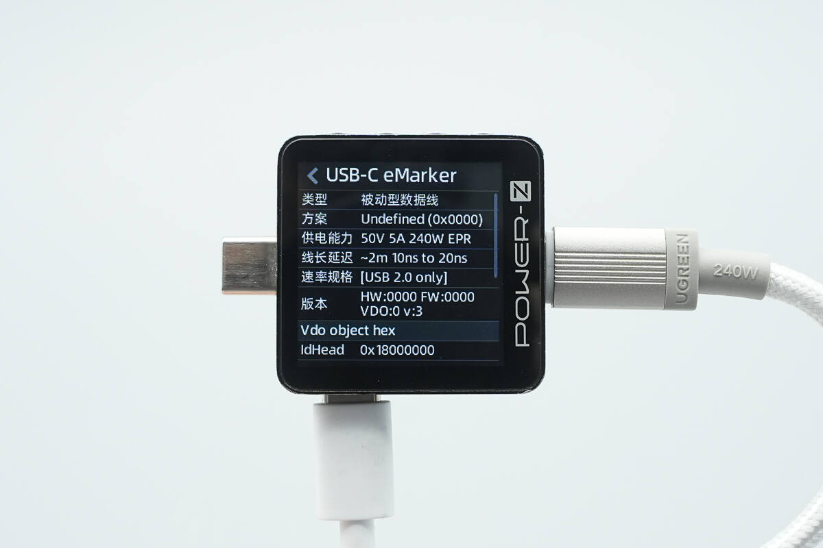
ChargerLAB POWER-Z KM003C shows it has an E-Marker chip, supports power delivery up to 50V/5A, and offers data transfer capability compliant with the USB 2.0 standard.
This side is printed with the UGREEN logo and “160W.”

The opposite side features the same printing.
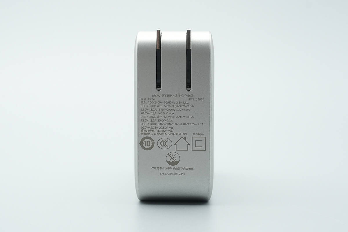
Below the foldable plug pins, the specifications are printed.

Model: X774
Input: 100-240V~ 50/60Hz 2.3A Max
USB-C1/C2 Output: 5V⎓3A / 9V⎓3A / 12V⎓3A / 15V⎓3A / 20V⎓5A / 28V⎓5A, 140.0W Max
USB-C3/C4 Output: 5V⎓3A / 9V⎓3A / 12V⎓2.5A, 30W Max
USB-A Output: 5V⎓3A / 9V⎓2A / 12V⎓1.5A / 10V⎓2.25A, 22.5W Max
Total Output Power: 160W Max
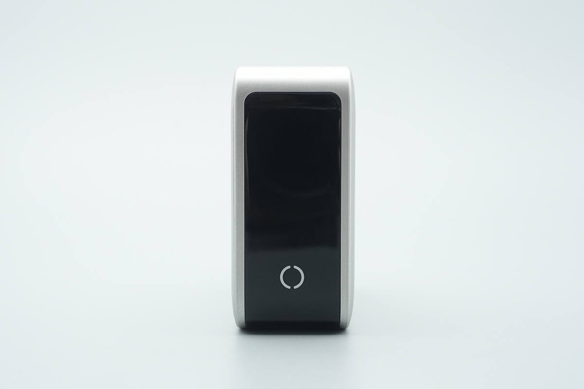
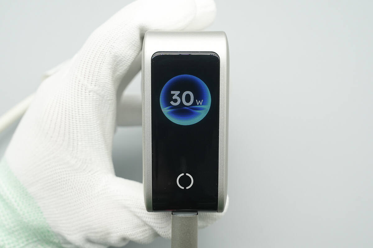
Close-up of the LCD screen and touch button.
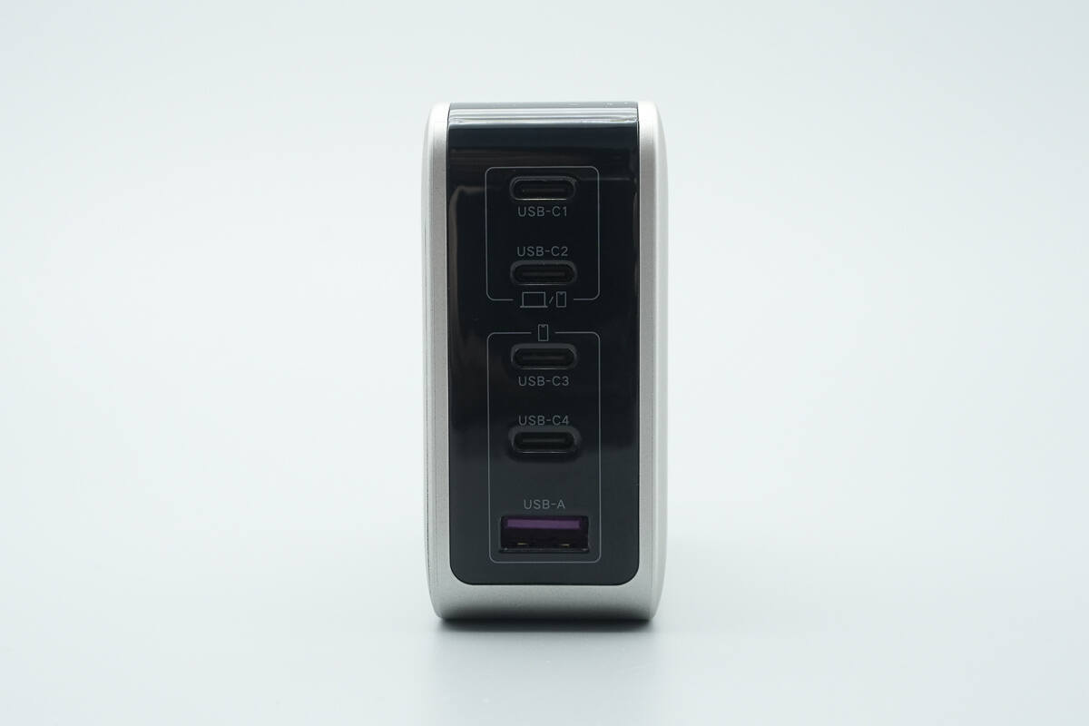
The output side features four USB-C ports and one USB-A port.
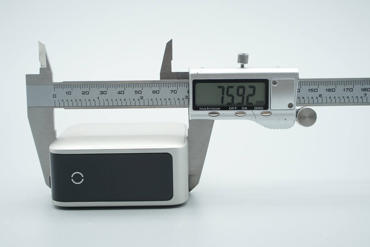
The length of the charger is about 75.9 mm (2.99 inches).
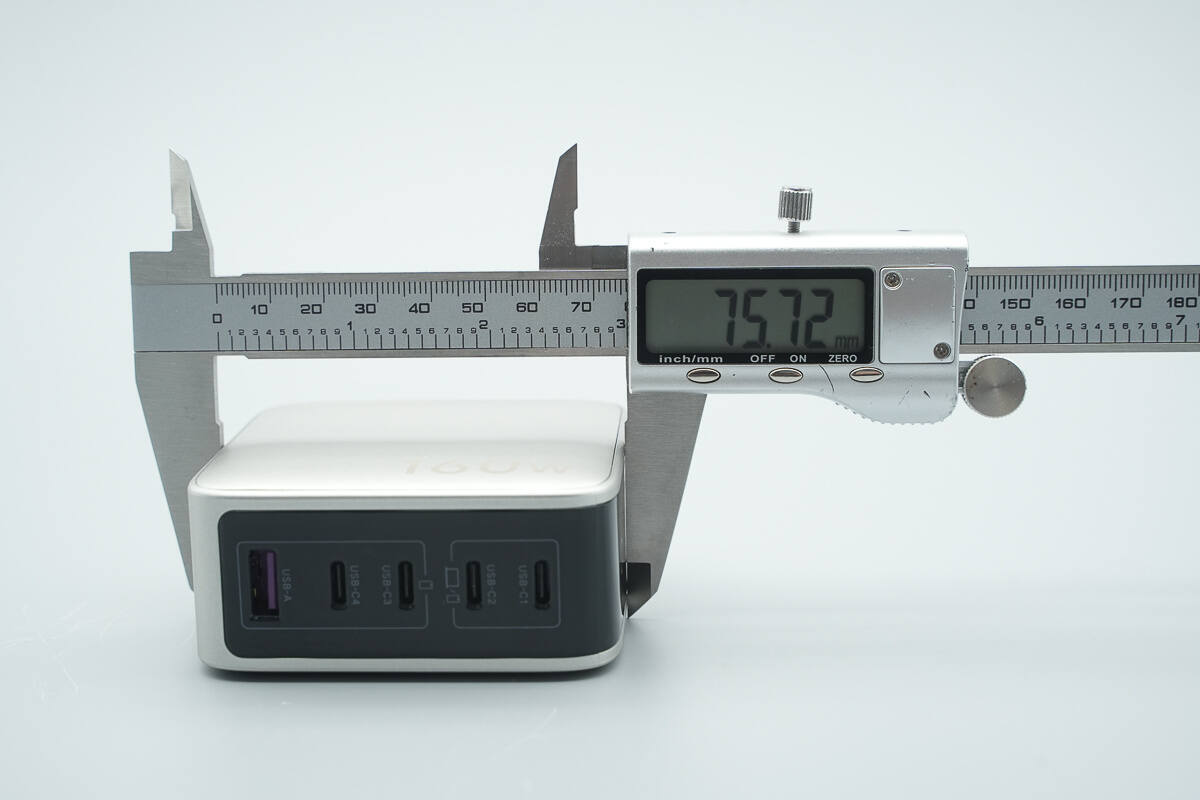
The width is about 75.7 mm (2.98 inches).
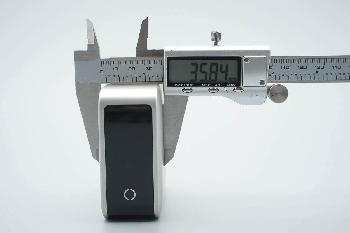
The thickness is about 35.8 mm (1.41 inches).
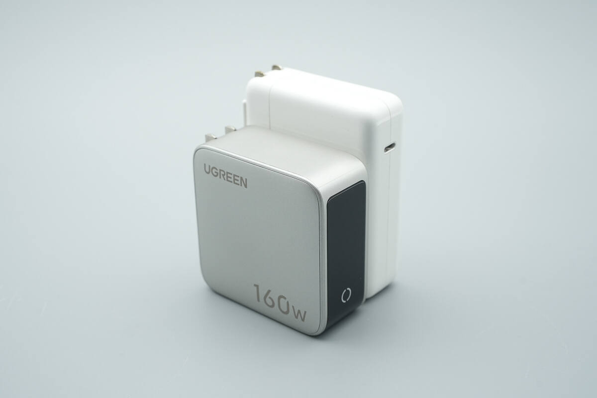
It is much smaller in size compared to Apple’s 140W charger.
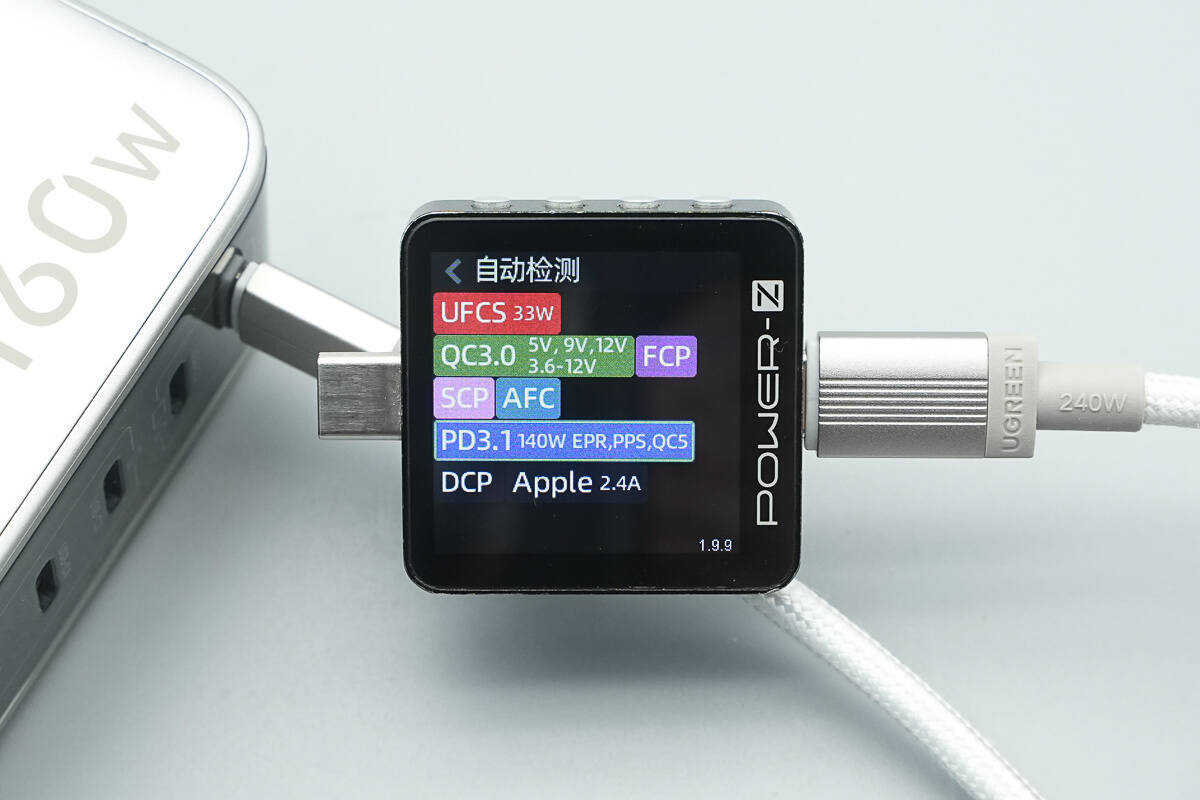
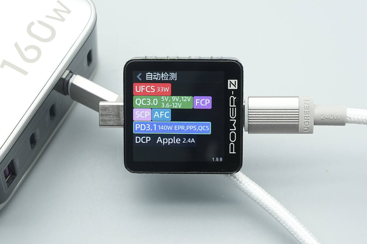
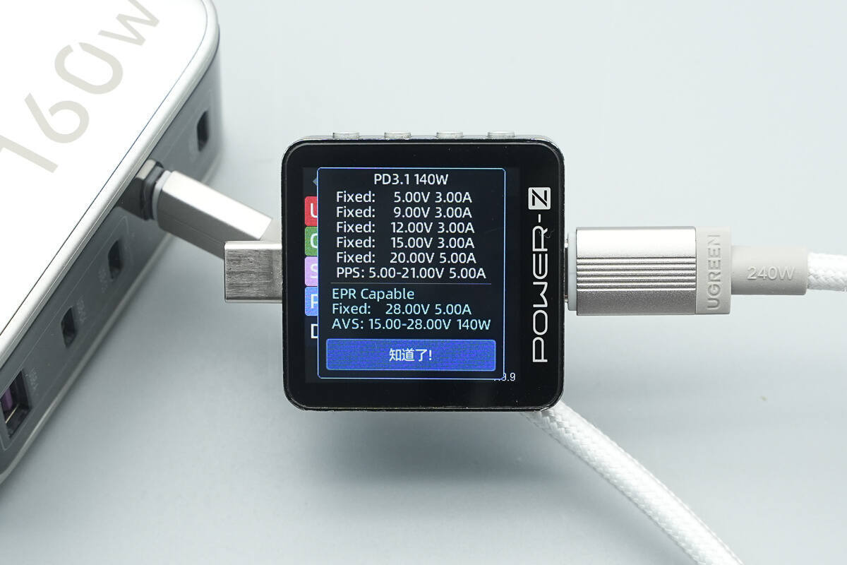
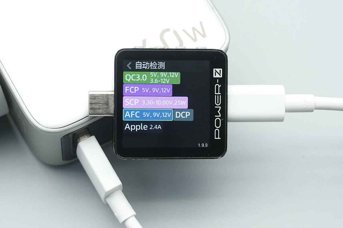
ChargerLAB POWER-Z KM003C shows that the USB-C1 supports UFCS, QC3.0/5, FCP, SCP, AFC, PD3.1, PPS, DCP, and Apple 2.4A charging protocols.

It features six fixed PDOs: 5V3A, 9V3A, 12V3A, 15V3A, 20V5A, and 28V5A, as well as a 5–21V5A PPS voltage range and a 15–285A AVS voltage range.
The USB-C2 port supports the same protocols as the USB-C1 port.
The PDO messages are also identical.
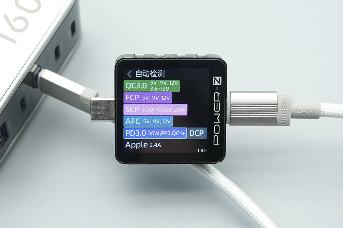
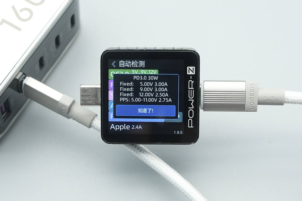
The USB-C3 port supports QC3.0/4+, FCP, SCP, AFC, PD3.0, PPS, DCP, and Apple 2.4A protocols.
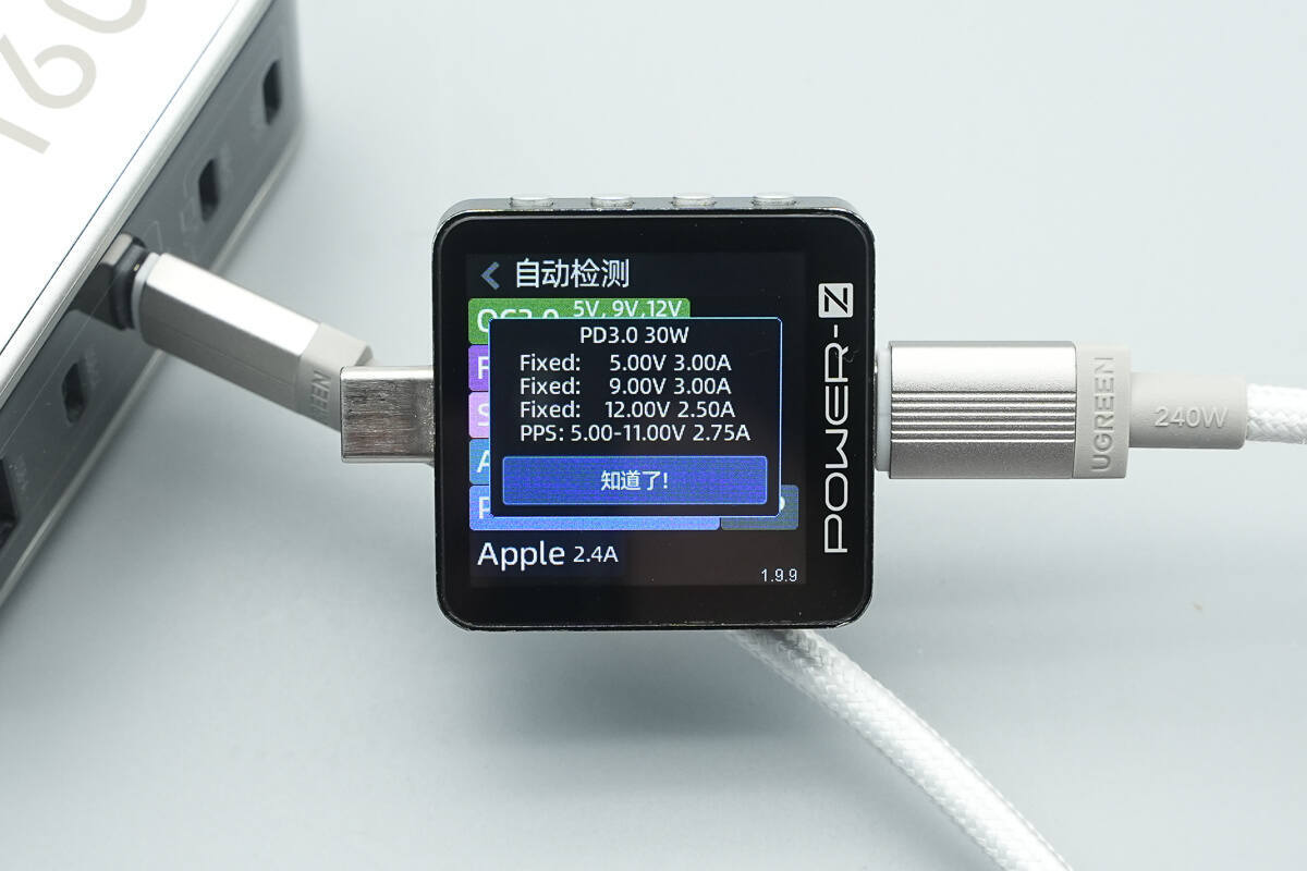
It has three fixed PDOs of 5V3A, 9V3A, and 12V2.5A, along with one set of PPS voltage level: 5-11V2.75A.

The USB-C4 port supports the same protocols as the USB-C3 port.
The PDO messages are also identical.
The USB-A port supports QC3.0, FCP, SCP, AFC, DCP, and Apple 2.4A protocols.
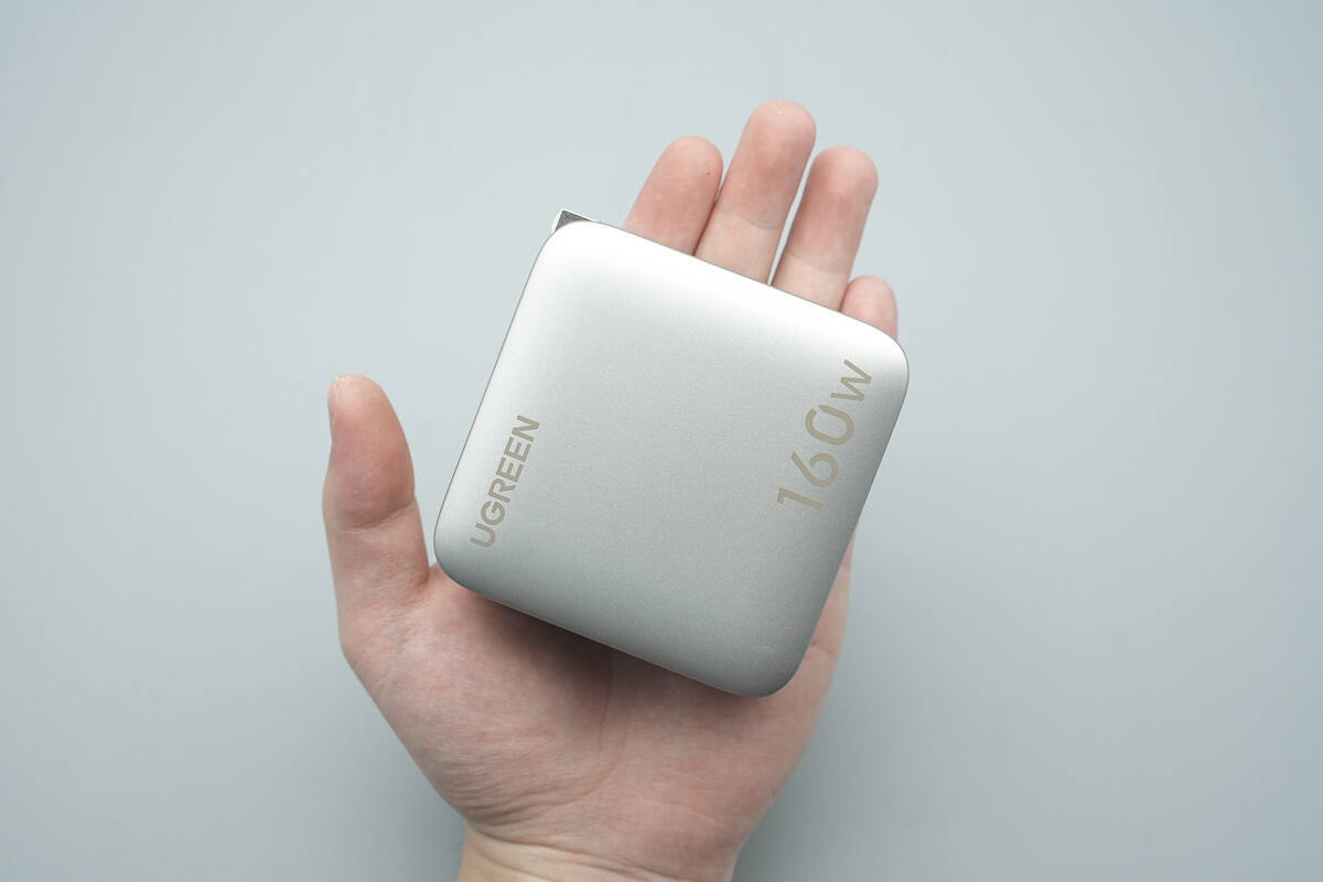
That's how big it is in the hand.
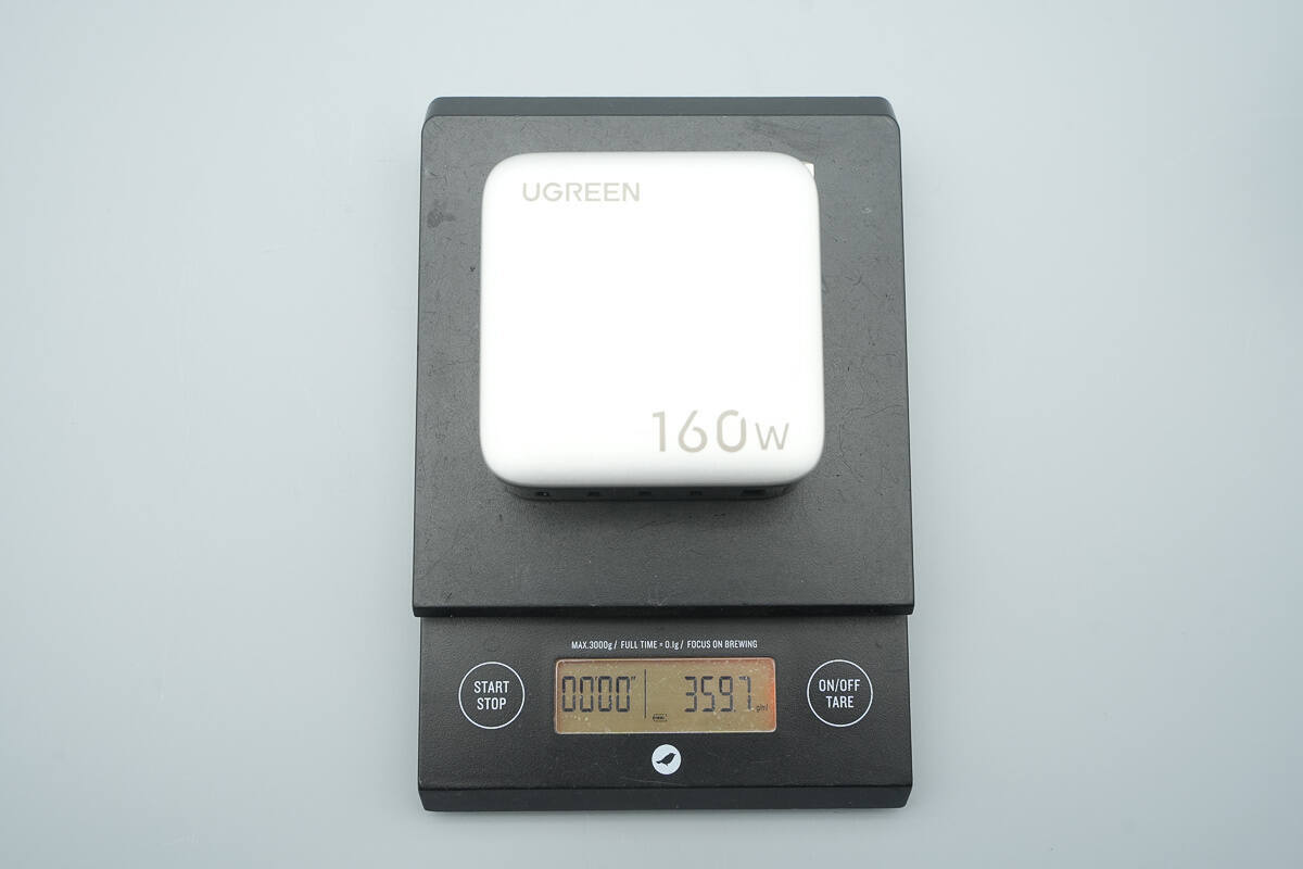
The weight is about 360 g (12.7 oz).
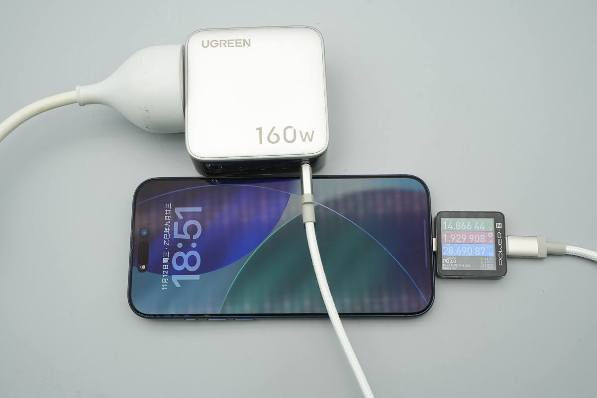
Use it to charge the iPhone 17 Pro Max.

The charger displays the PD charging protocol, with an output voltage of 15.1V and an output current of 2A.
The displayed output power is 30W.
Teardown
Next, let's take it apart to see its internal components and structure.
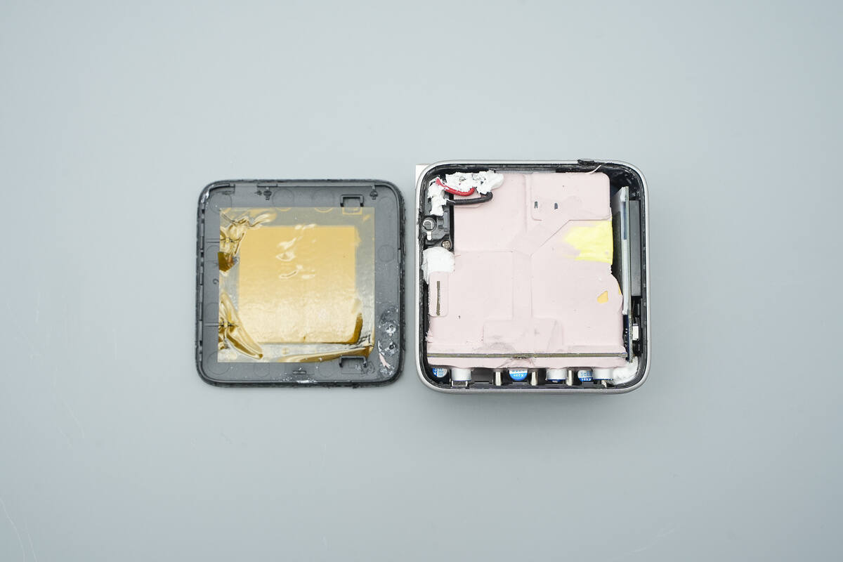
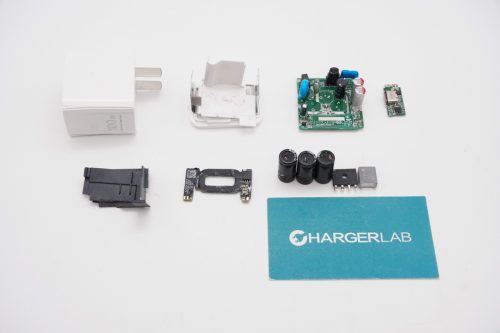
Pry open the casing along the seams.

Inside, there are high-temperature adhesive tapes and a graphite thermal pad.
The PCBA module is covered with potting compound.

The foldable plug pins are connected to the PCBA module via soldered wires.
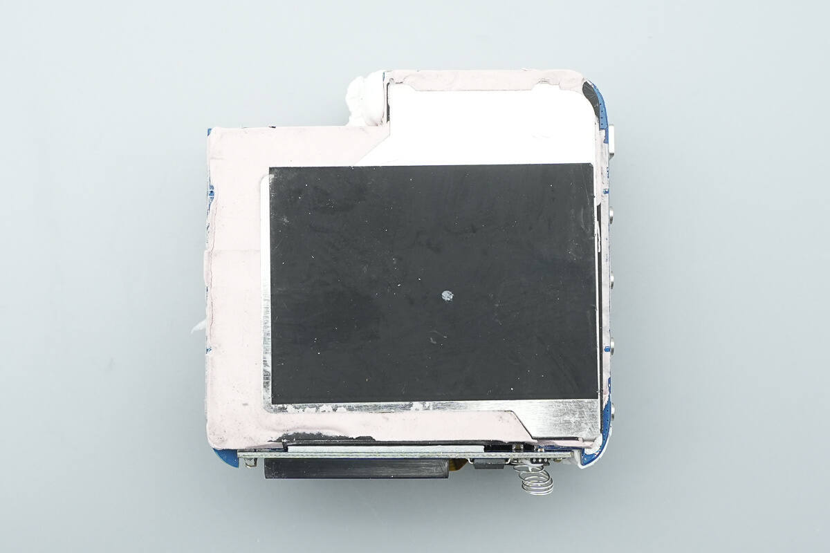
The screen is connected to the PCBA module via a connector.
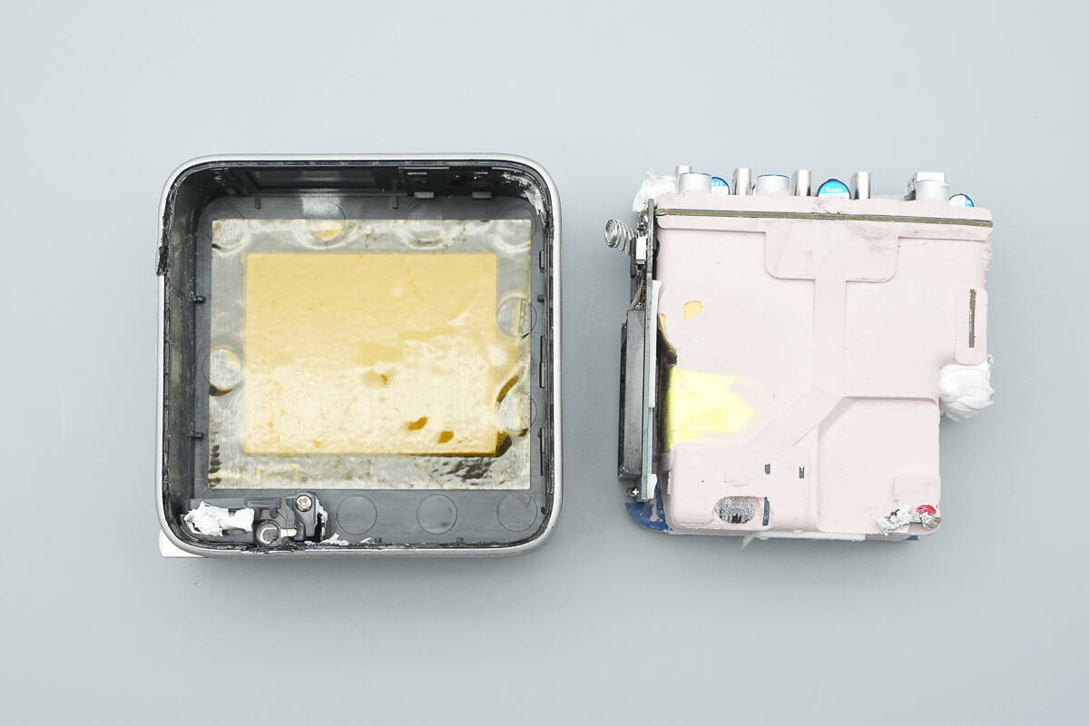
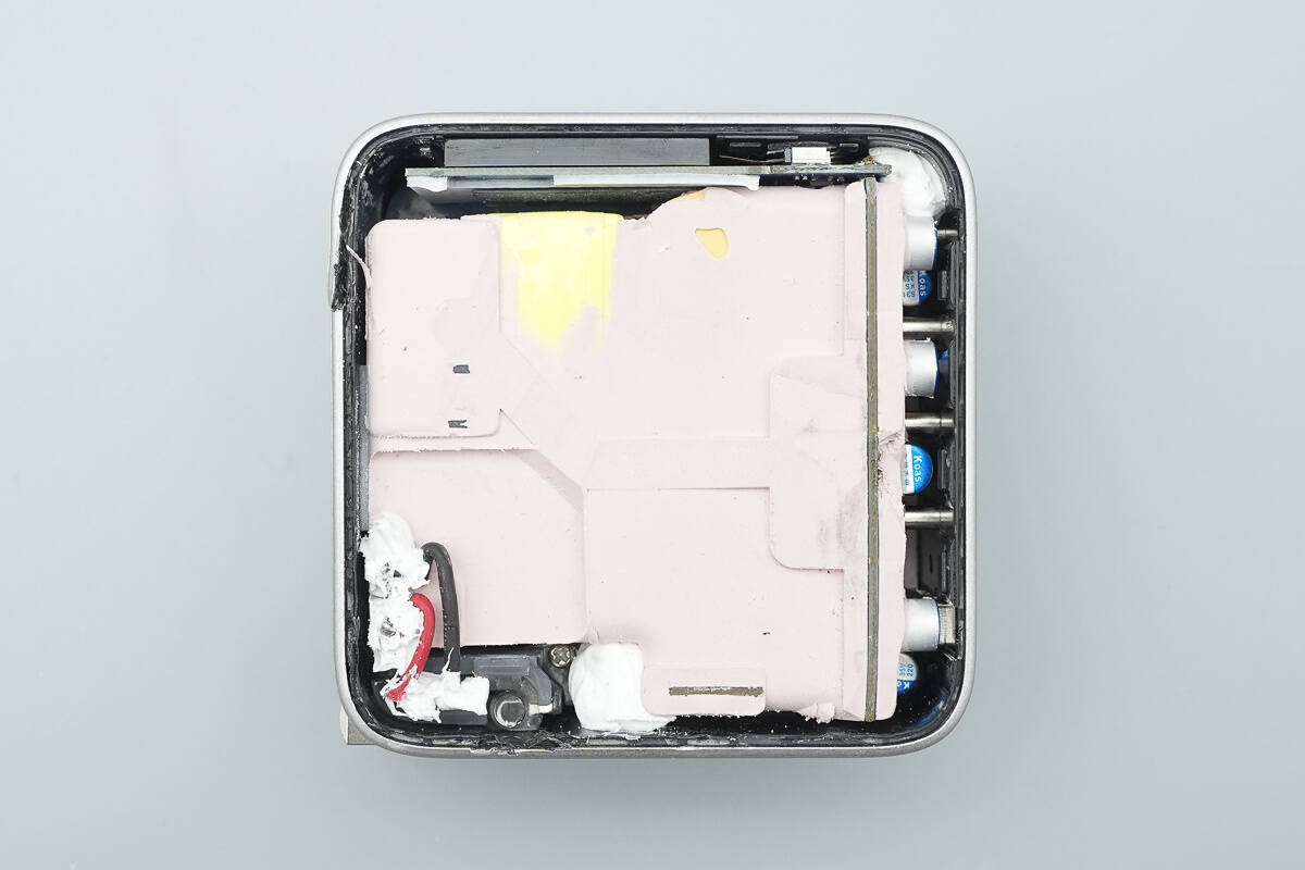
After removing the PCBA module, graphite thermal pads are visible inside the casing.
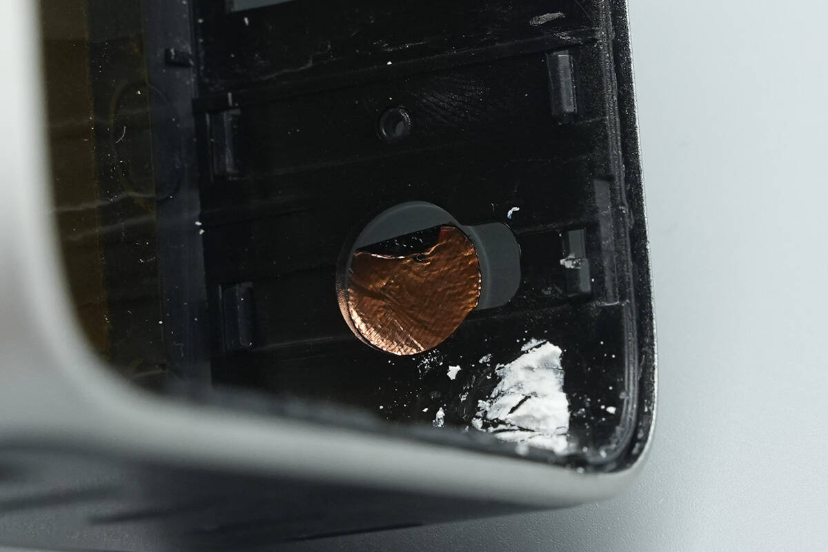
The touch button area has copper foil to increase the sensing area.
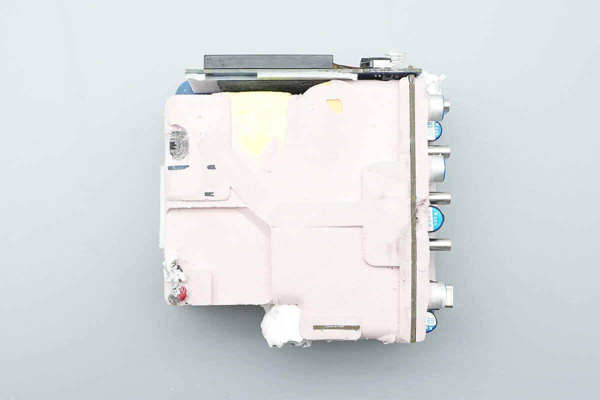
The PCBA module is encapsulated with thermal adhesive.
On the back, there is a metal plate with a graphite thermal pad attached for heat dissipation.
The length of the PCBA module is about 67.7 mm (2.67 inches).
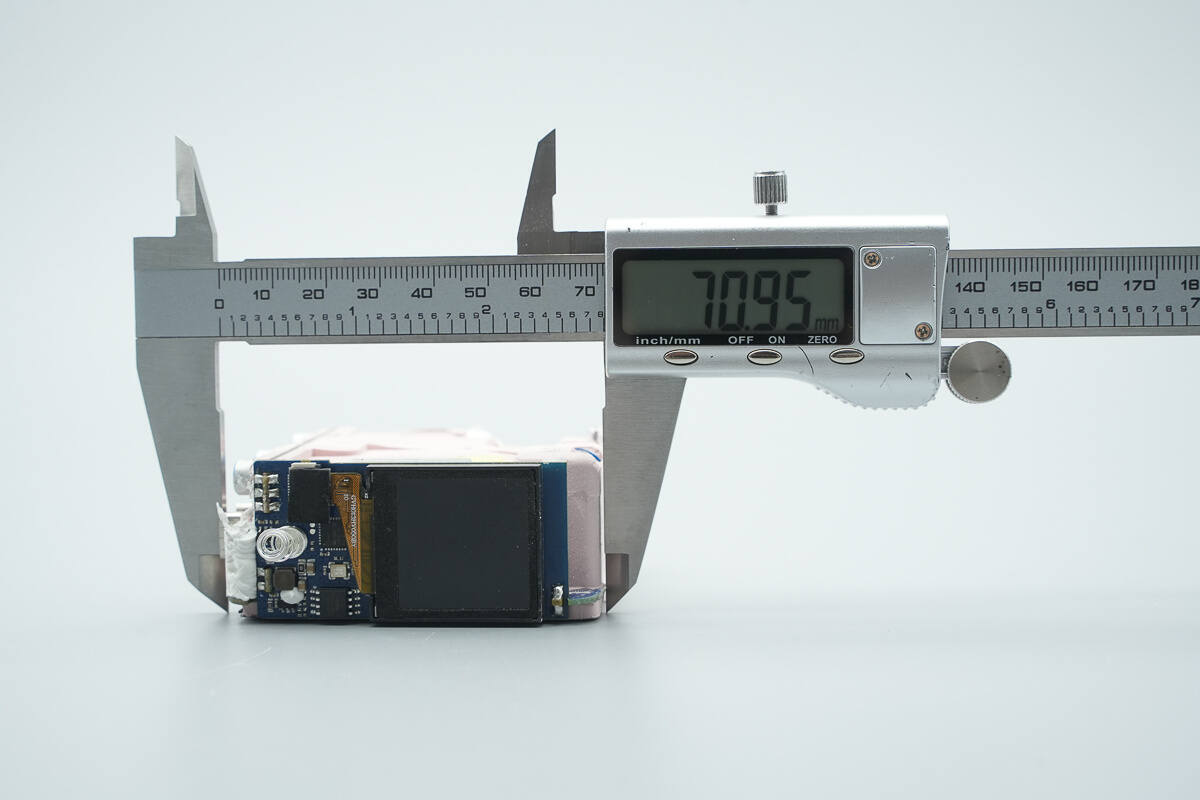
The width is about 71 mm (2.8 inches).
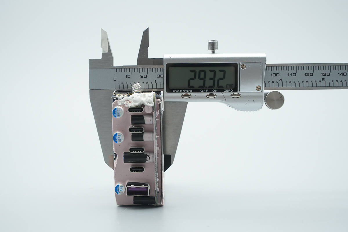
The thickness is about 29.3 mm (1.15 inches).

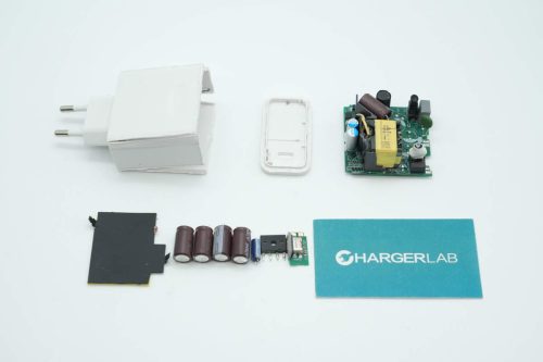
The PCBA module is composed of multiple small PCBs soldered together. On the lower left side is the input section, which includes a fuse, thermistor, temperature switch, common mode choke, and safety X2 capacitor. Above it are the common mode choke, rectifier bridge PCB, and filter PCB. On the right side is the PFC boost inductor, with a transformer located at the lower right. Beneath the transformer are the synchronous rectification PCB and filter solid-state capacitors. At the top is the LCD screen PCB, and on the right side are the output PCB and additional filter solid-state capacitors.
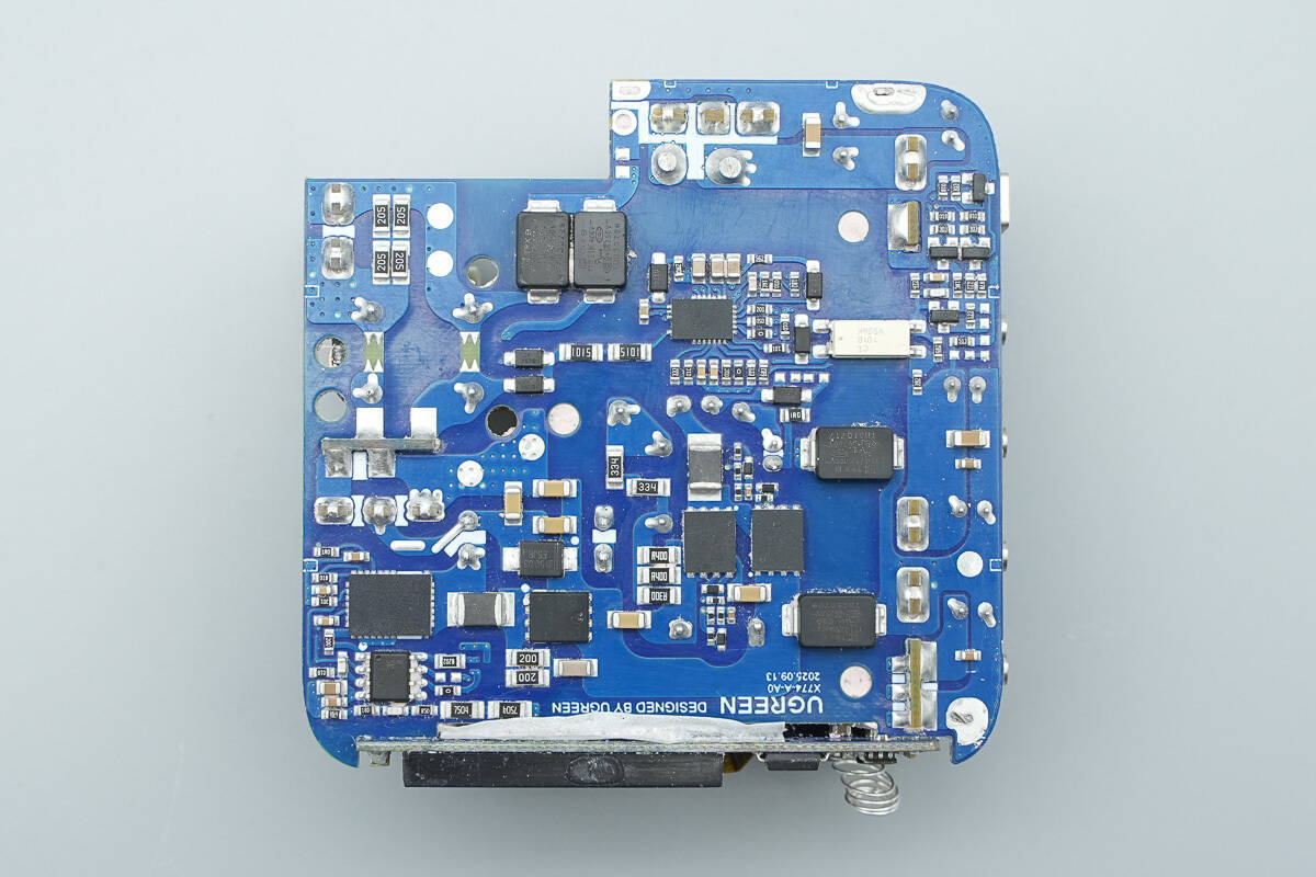
On the back, there is a PFC controller, a GaN monolithic chip, a SiC diode, an AHB controller, a GaN switch, SMD Y-capacitors, and a feedback optocoupler.

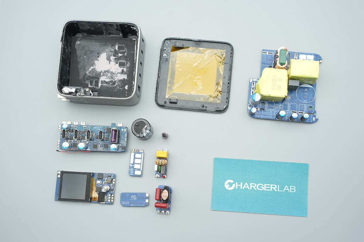
Remove each of the small PCBs.
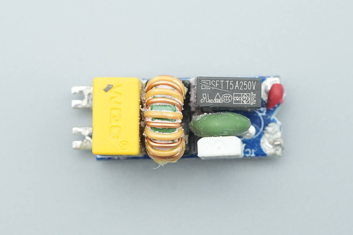
The input PCB contains a fuse, NTC thermistor, temperature switch, common-mode choke, and a safety X2 capacitor.
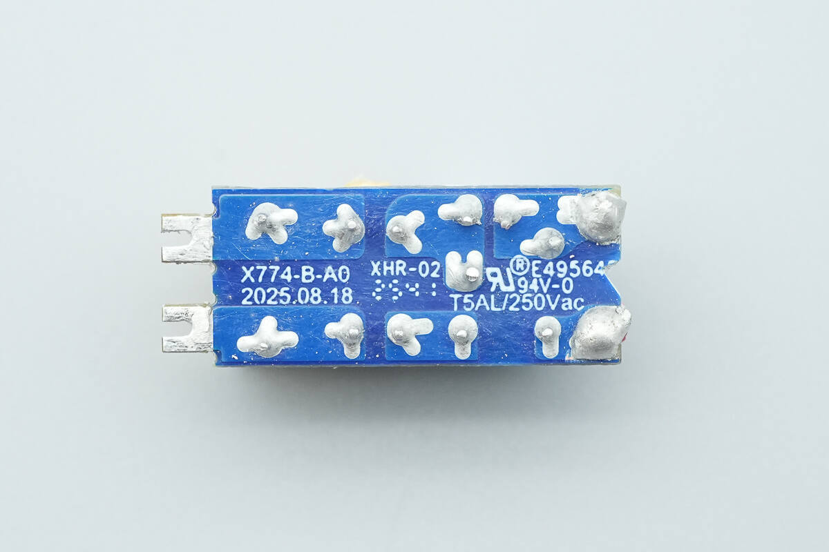
The back side has no components.
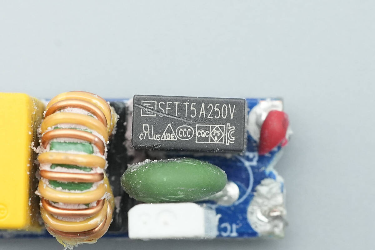
The input fuse is from Chevron, rated at 5A 250V.

The NTC thermistor, model HNP2R509, is used to suppress inrush current at power-on.

The temperature protector is from HKW, model HKW9700, with a trigger temperature of 65°C. It shorts the thermistor after the charger heats up during normal use to eliminate power loss.

The common mode choke is wound with enamel-coated wire and insulated wire.
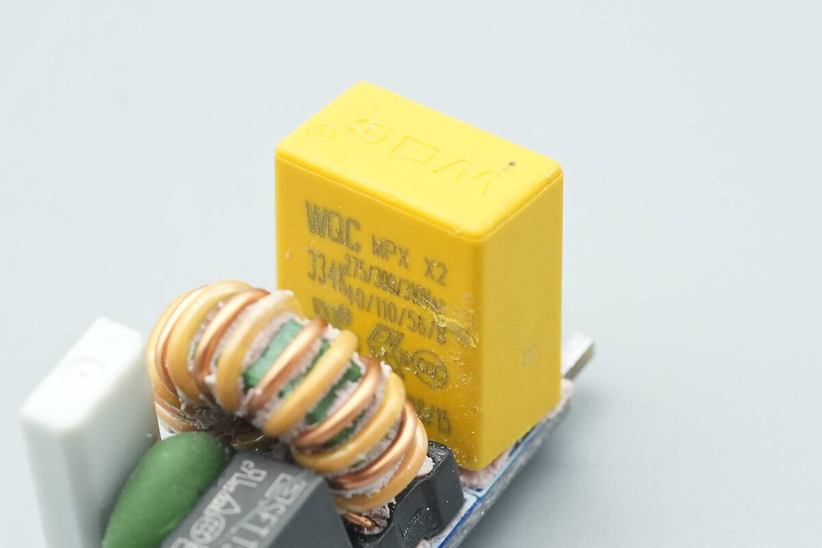
The safety X2 capacitor is from WQC, with a rating of 0.33 μF.
The common mode choke is wound with flat copper wire.
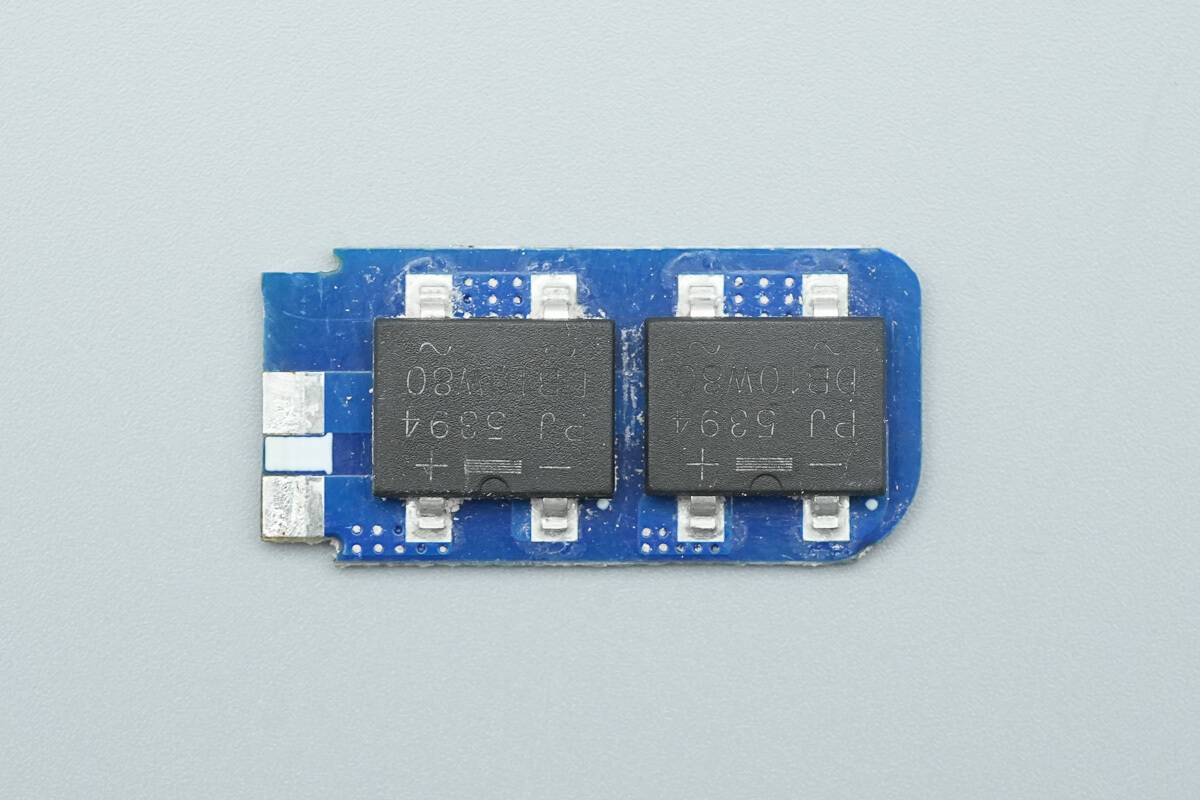
The bridge rectifiers are soldered onto a vertical small PCB, with two units connected in parallel to evenly distribute heat.
The back side has no components.
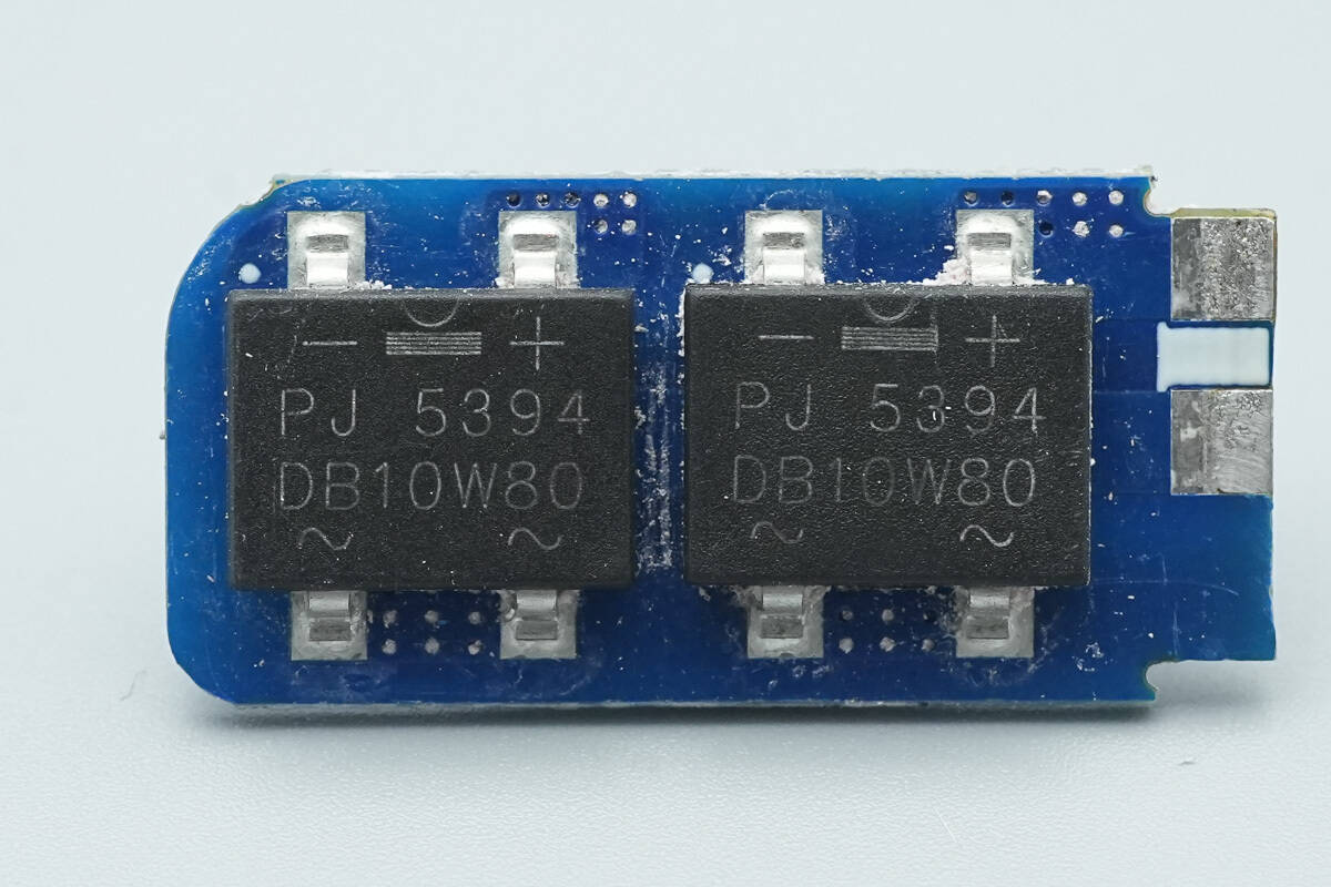
The bridge rectifier is from PANJIT, marked DB10W80.
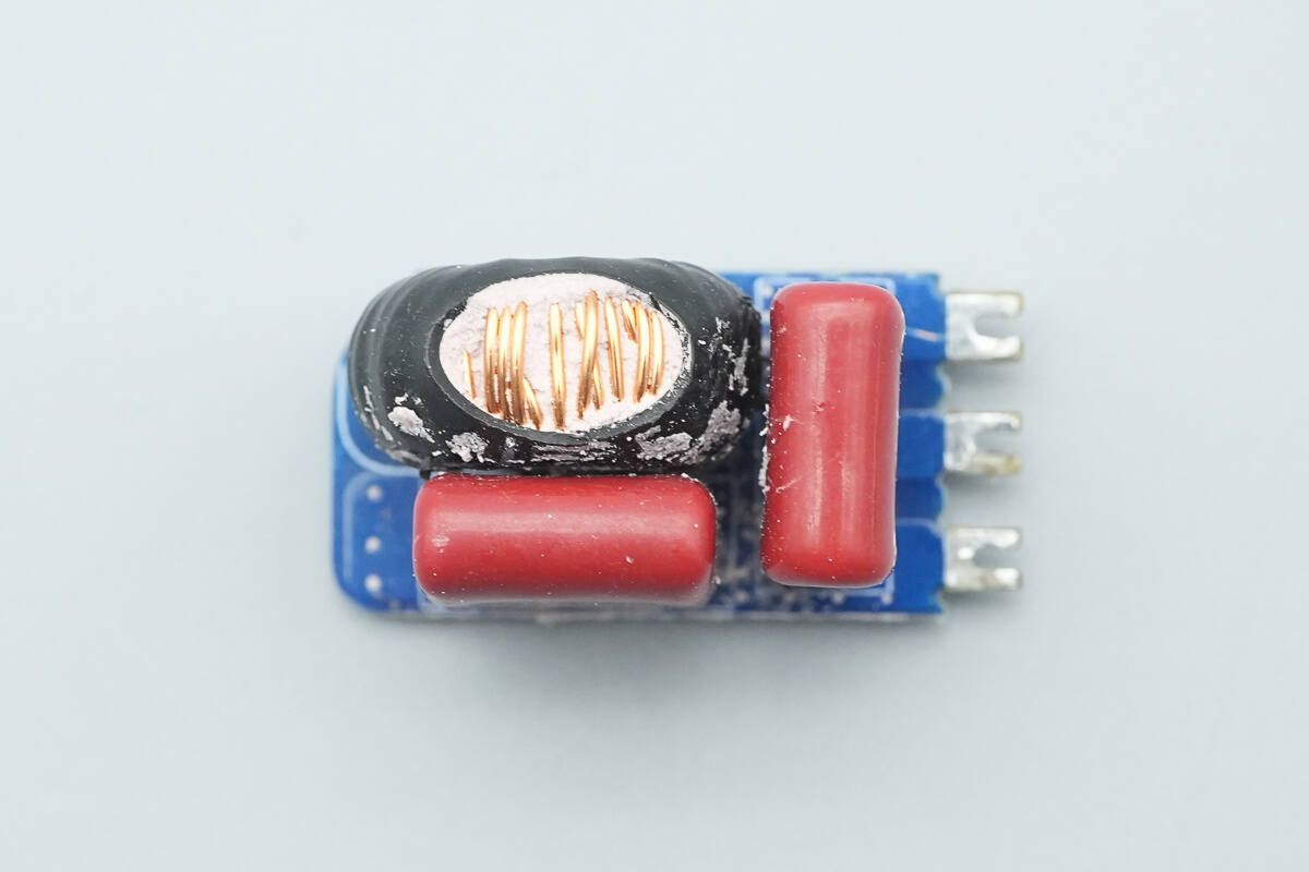
The front of the filter PCB has two film capacitors and a filter inductor.
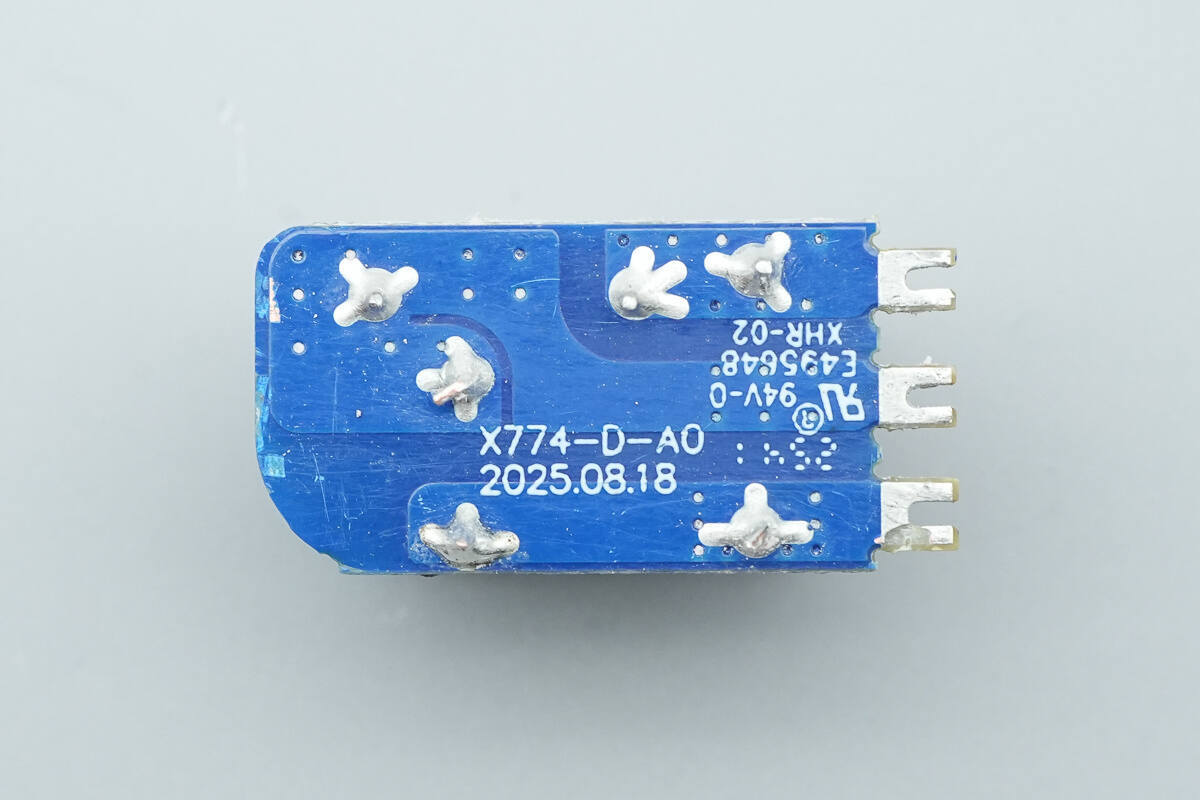
The back side has no components.
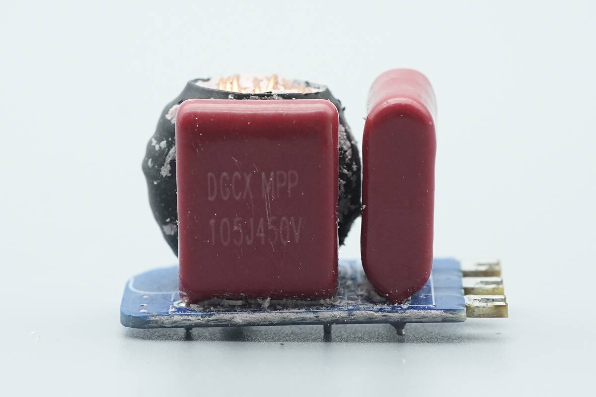
The film capacitors are from DGCX, each rated at 1 μF.
The filter inductor is wrapped with heat-shrink tubing for insulation.
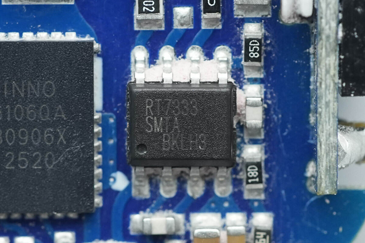
The PFC controller is from RICHTEK, model RT7333. It supports operating frequencies of 130 kHz, 180 kHz, 240 kHz, and 400 kHz, providing flexibility for different power conversion requirements. It can directly drive GaN or MOSFET devices, further improving system efficiency and simplifying the design. The controller comes in an SOP-8 package.
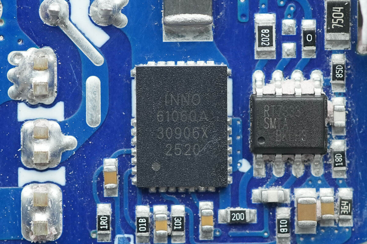
The PFC MOSFET is from Innoscience, model ISG6106QA. It is a GaN chip that integrates a GaN FET and lossless current sensing. The chip features a 700V-rated enhancement-mode GaN FET with a transient voltage tolerance of 800V and an on-resistance of 100 mΩ. Internally, it includes a smart programmable driver and a high-voltage linear regulator.
The ISG6106QA has ultra-low quiescent current and an automatic standby function, supports switching frequencies up to 2 MHz, and integrates a 5V regulated output for powering digital isolators. It also includes undervoltage lockout, overcurrent protection, and overtemperature protection. The chip is suitable for PFC, flyback, half-bridge, and full-bridge applications, meeting the requirements of PD fast charging, LED lighting, and solar inverters. It comes in a QFN 6×8 mm package.
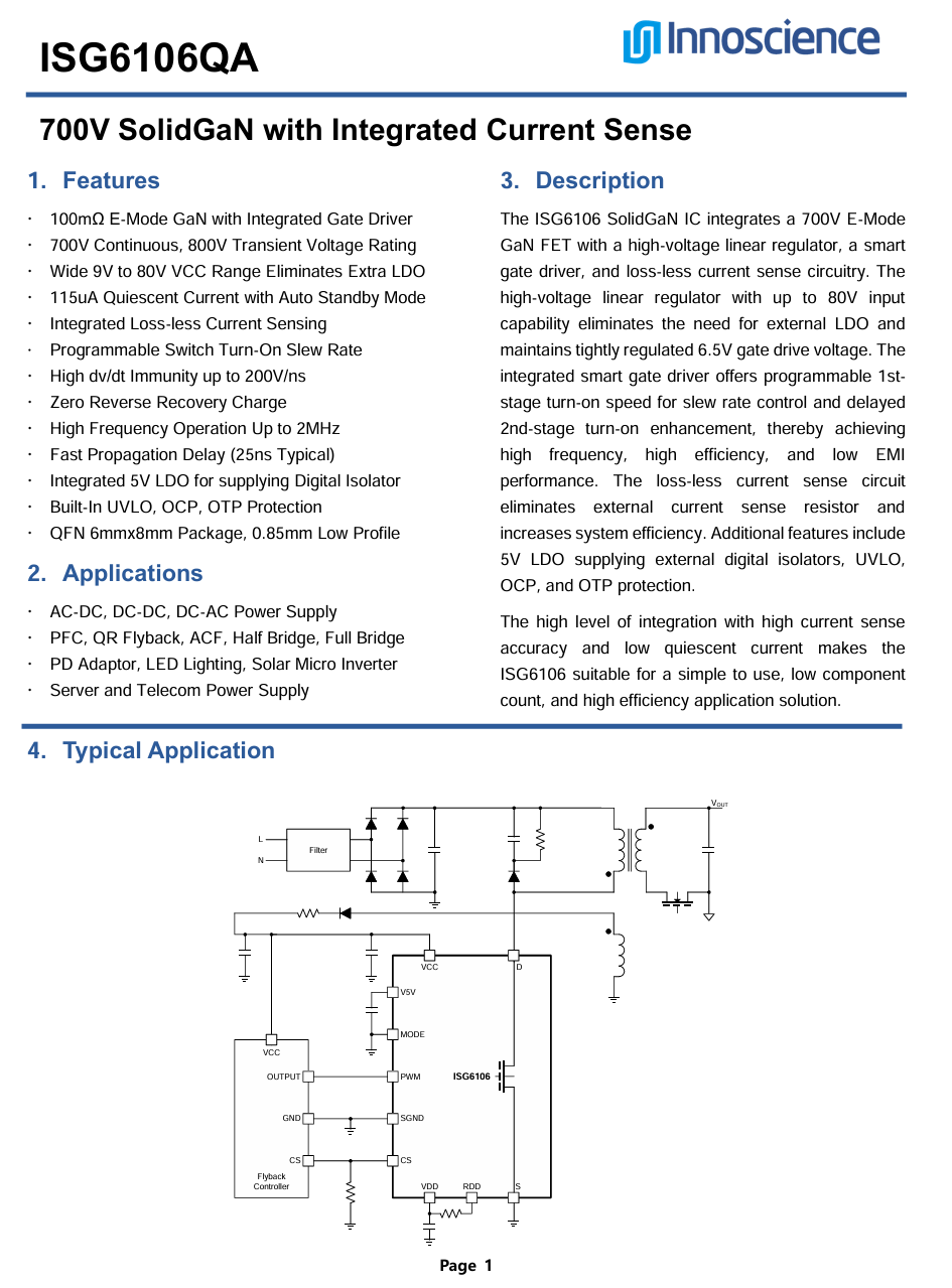
Here is the information about Innoscience ISG6016QA.
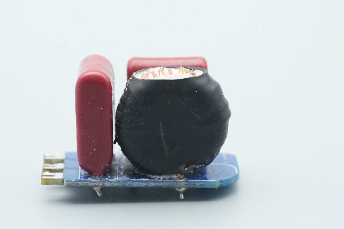
The PFC boost inductor is tightly wrapped with tape for insulation.
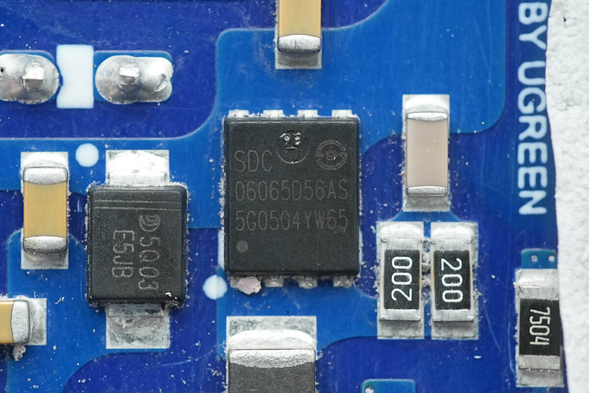
The PFC rectifier is from SiCRED, model SDC06065D56AS. It is a SiC diode rated at 650 V, 6 A, and comes in a DFN 5×6 mm package.

The bypass diode is from Jingdao Microelectronics, model ES5JBF. It is rated at 600 V, 5 A, and comes in an SMBF package.
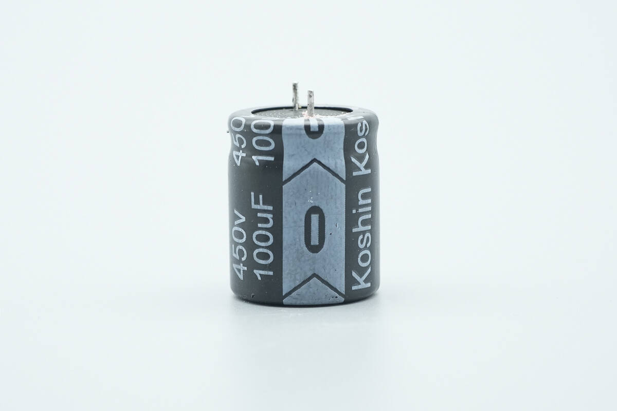
The high-voltage filter capacitor is from Koshin, rated at 450 V, 100 μF.

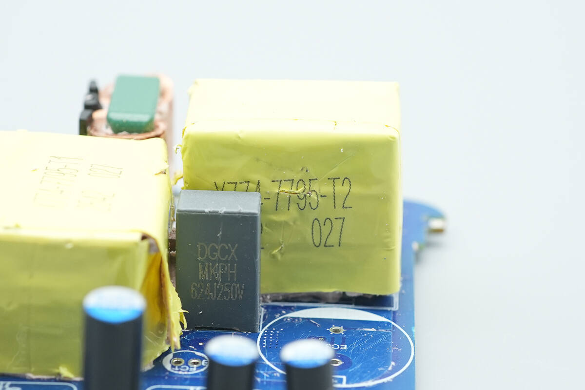
The master control chip is from RICHTEK, model RT7795M. It is a PWM controller specifically designed for asymmetrical half-bridge (AHB) power converters. The chip integrates a 625 V high-voltage startup device, supports output power up to 300 W, and output voltages from 5–48 V. It features built-in X-capacitor discharge and operates in a continuous resonant mode, effectively reducing power loss in the secondary-side synchronous rectifiers.
The RT7795M integrates a driver capable of directly driving GaN or MOSFET devices, simplifying the design. Its VCC range is 11–63.2 V. Additionally, the chip can control the PFC switch to further enhance design flexibility and efficiency, making it suitable for various power conversion applications. It comes in a WQFN-24L package.
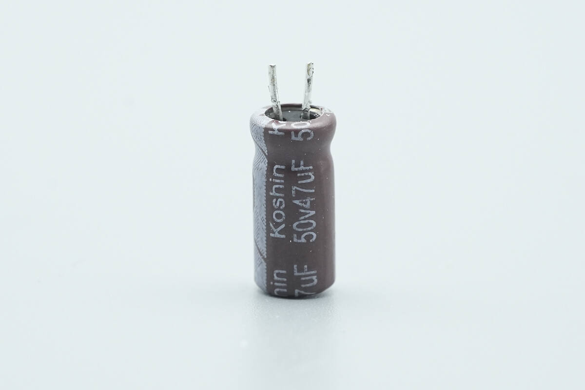
The filter capacitor powering the master control chip is from Koshin, rated at 50 V, 47 μF.
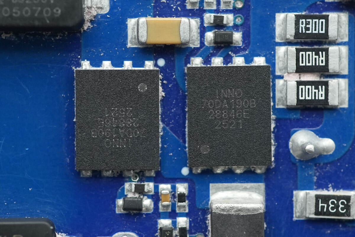
The AHB MOSFETs are from Innoscience, model INN700DA190B. These are enhancement-mode GaN transistors rated at 700 V, upgraded from the original 650 V rating, with a transient voltage tolerance of 800 V. The on-resistance is 190 mΩ, supporting higher power applications.
They support ultra-high switching frequencies, have no reverse-recovery charge, and feature very low gate and output charges. The devices meet JEDEC-standard industrial requirements, include built-in ESD protection, and comply with RoHS, lead-free, and EU REACH regulations. They are suitable for high-efficiency, high-density applications such as AC-DC and DC-DC conversion. The package is DFN 5×6 mm.
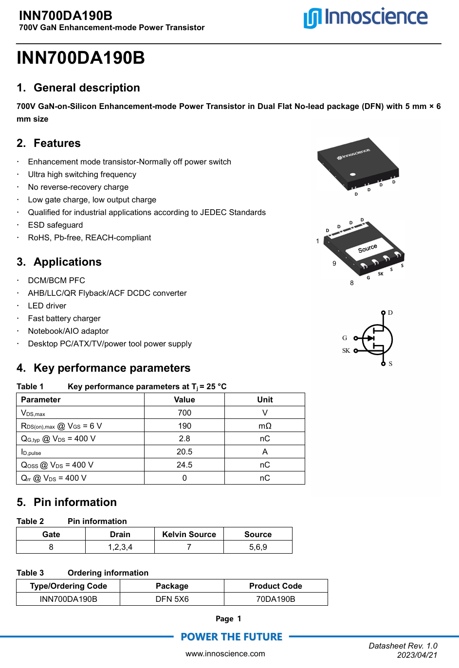
Here is the information about Innoscience INN700DA190B.

The resonant capacitor is from DGCX, rated at 0.62 μF, 250 V.
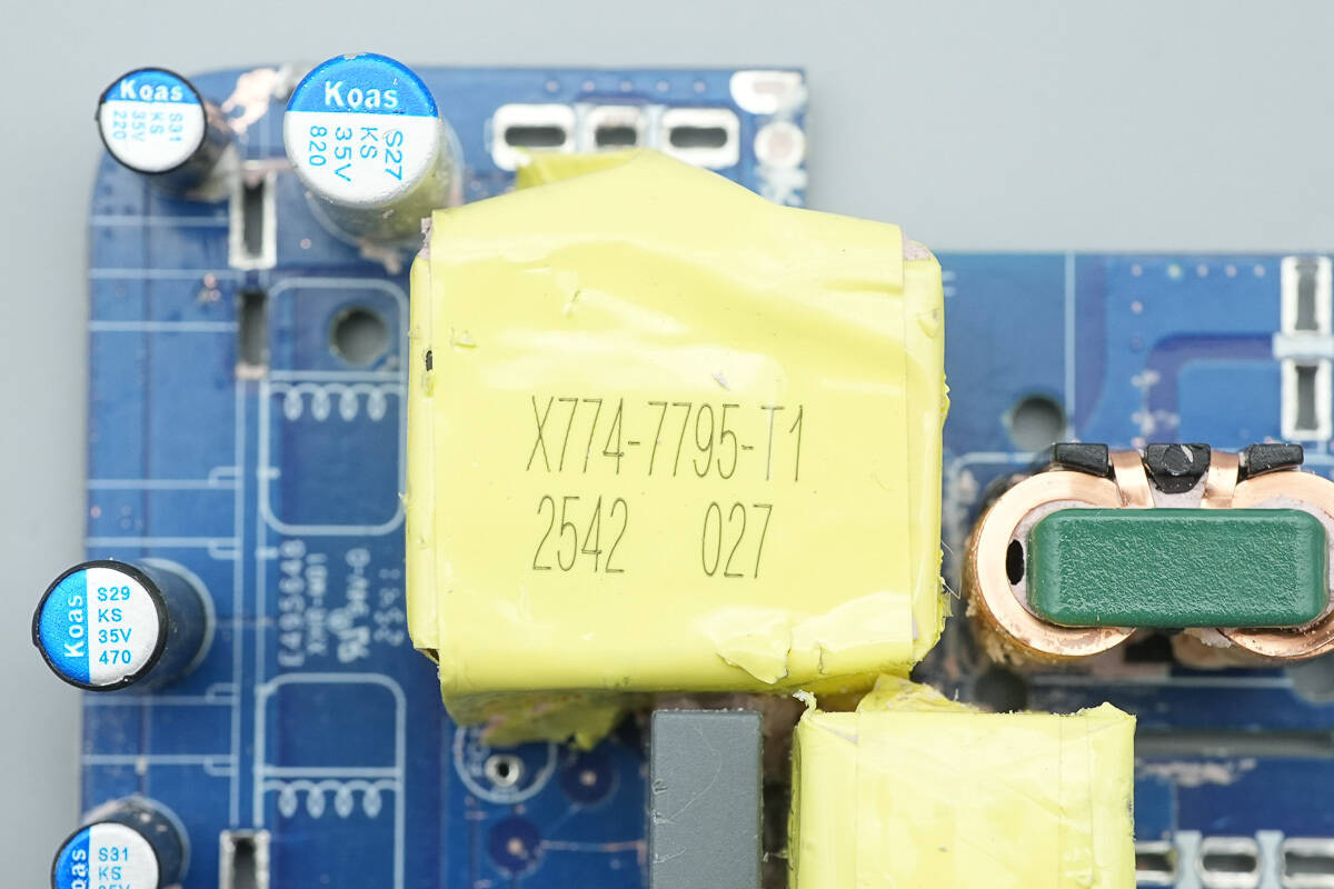
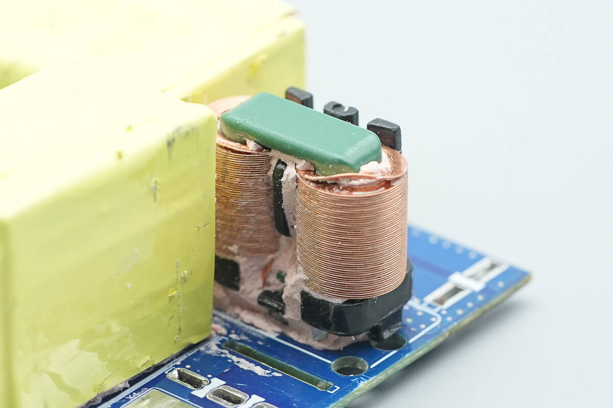
The transformer is insulated with tape wrapping.
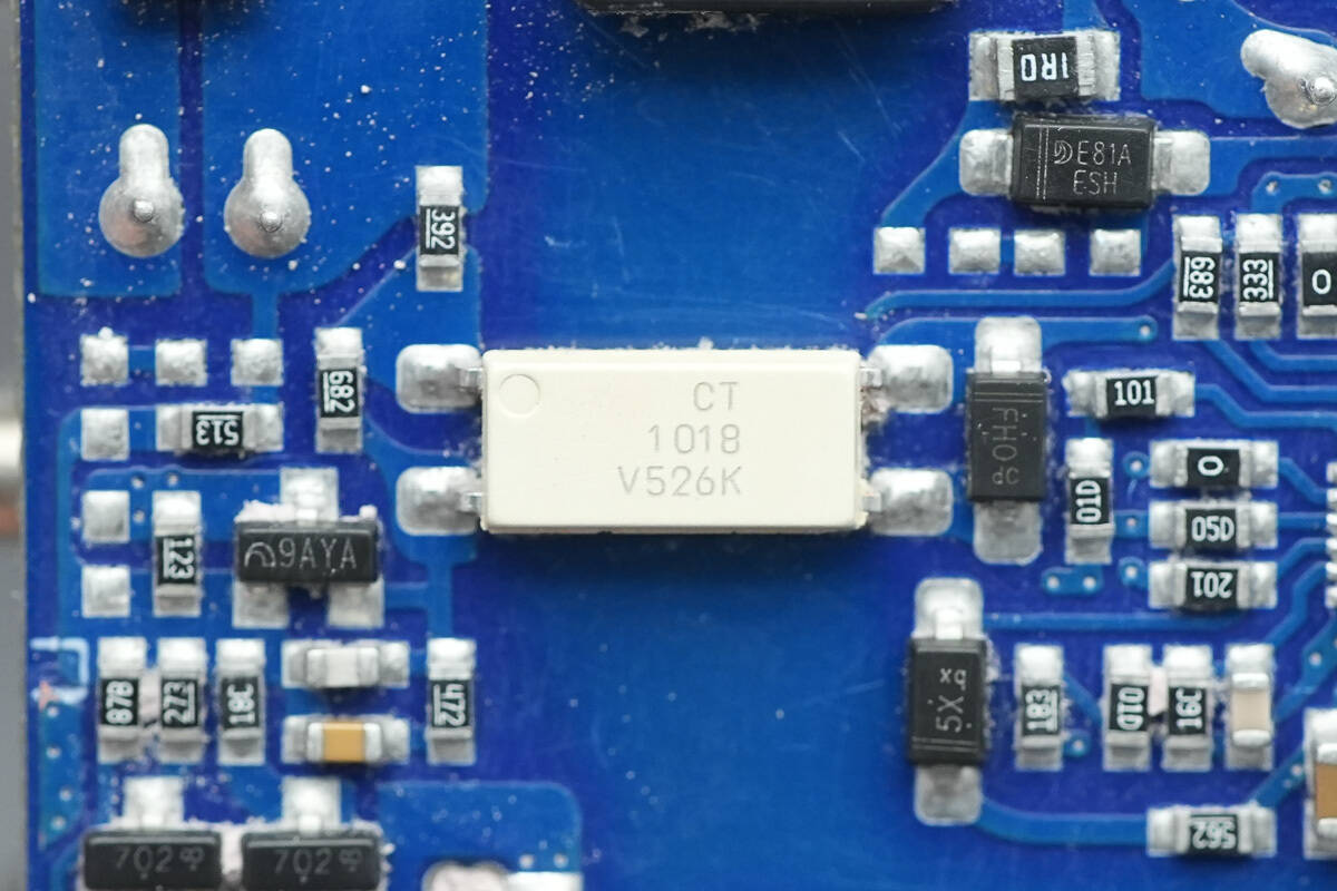
The CTMICRO CT1018 optocoupler is used for output voltage feedback.
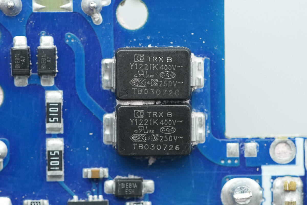
The SMD Y capacitors are from TRX, part number TMY1221K. Their compact size and light weight make them well-suited for high-density power products such as GaN fast chargers.

This SMD Y capacitor has the part number TMY1471K.
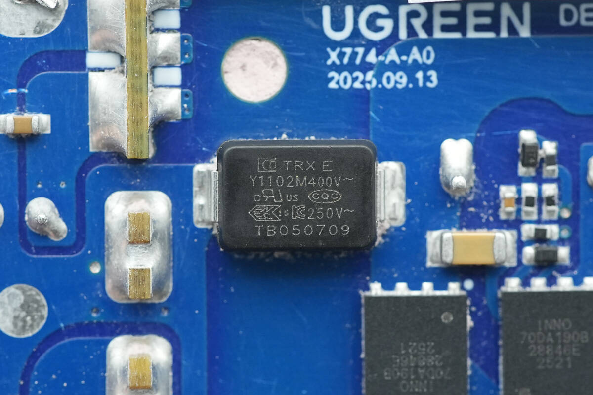
The other SMD Y capacitor has the part number TMY1102M.
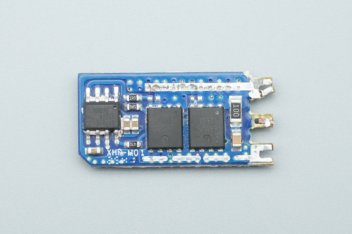
One side of the synchronous rectification PCB features a synchronous rectifier controller and two synchronous rectifier MOSFETs.

The other side is soldered with copper pads to increase the heat dissipation area.
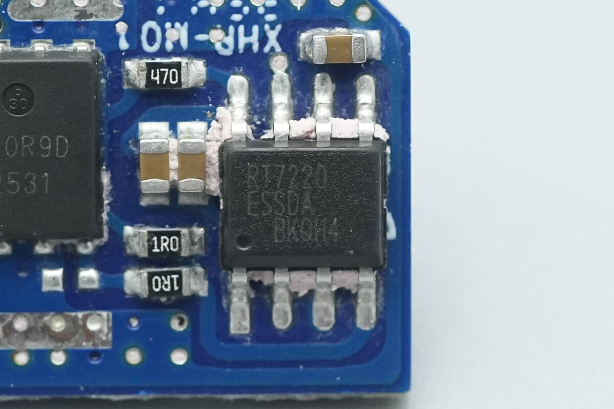
The synchronous rectifier controller is from RICHTEK, model RT7220E. It supports asymmetrical half-bridge (AHB) conversion and operates in CRM, CSM, and BM modes. The RT7220E controls the SR gate switching by detecting the MOSFET drain voltage. This function minimizes the dead time during turn-off and transfers sinusoidal energy through SR gate pulses, thereby improving overall efficiency.
It supports a wide output voltage range of 5–48 V and integrates a high-voltage, low-dropout linear regulator to power the MOSFET gate driver at low output voltages. When used with the RT7795 AHB controller, it can enable a dual-pulse function to optimize efficiency under heavy load or low-output conditions. The package is SOP-8.
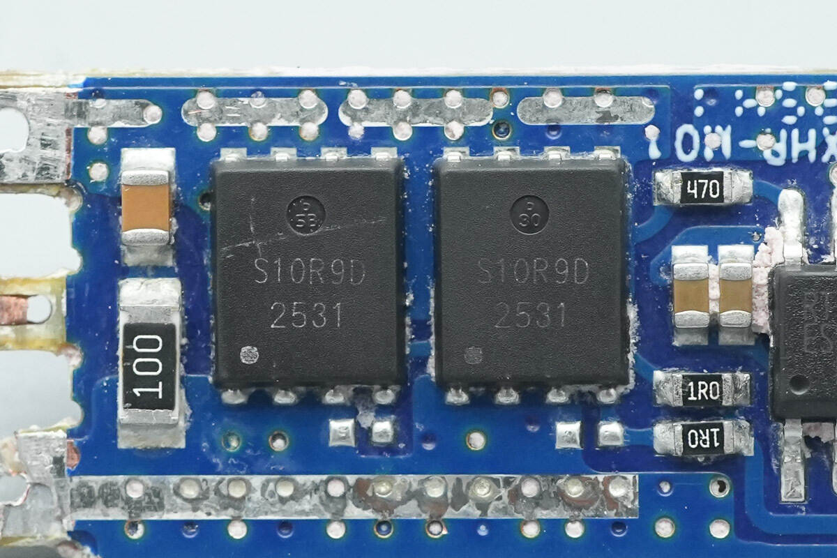
The synchronous rectifiers are from Prisemi, marked S10R9D, model PSM8N10R9D. They are NMOS devices rated at 100 V with an on-resistance of 6.8 mΩ, packaged in PDFN 5×6 mm, 8L.
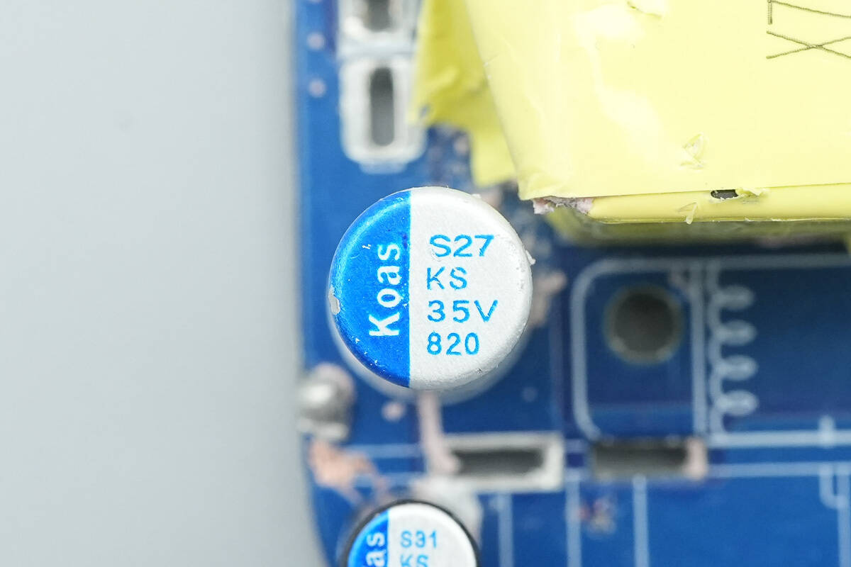
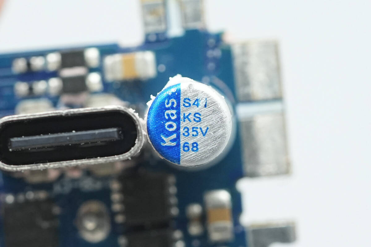
The filter capacitor is from Koshin, part of the KS series of polymer conductive solid capacitors, rated at 35 V, 820 μF.

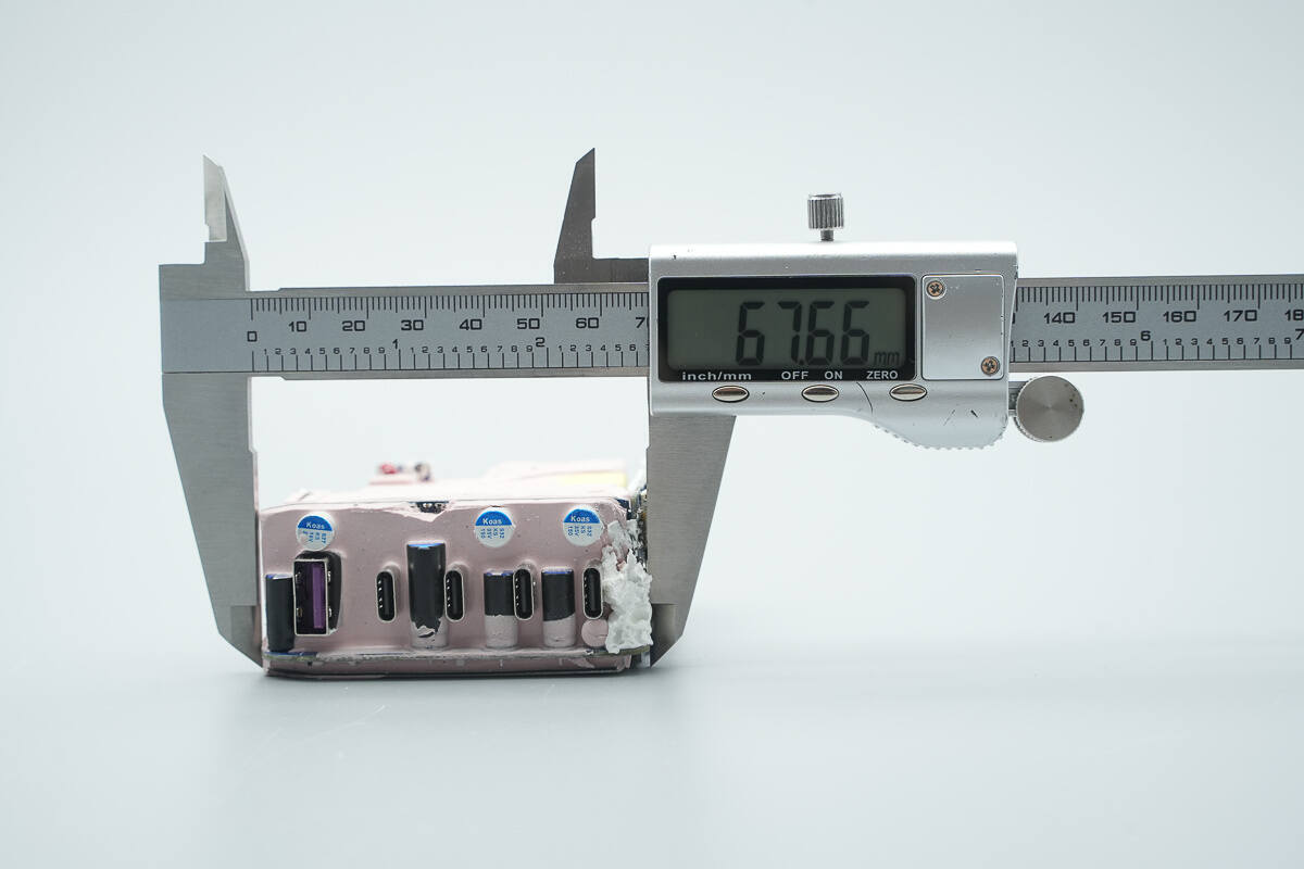
The output section features a buck PCB and filter capacitors.

The other filter capacitor is rated at 35 V, 220 μF and is insulated with heat-shrink tubing.
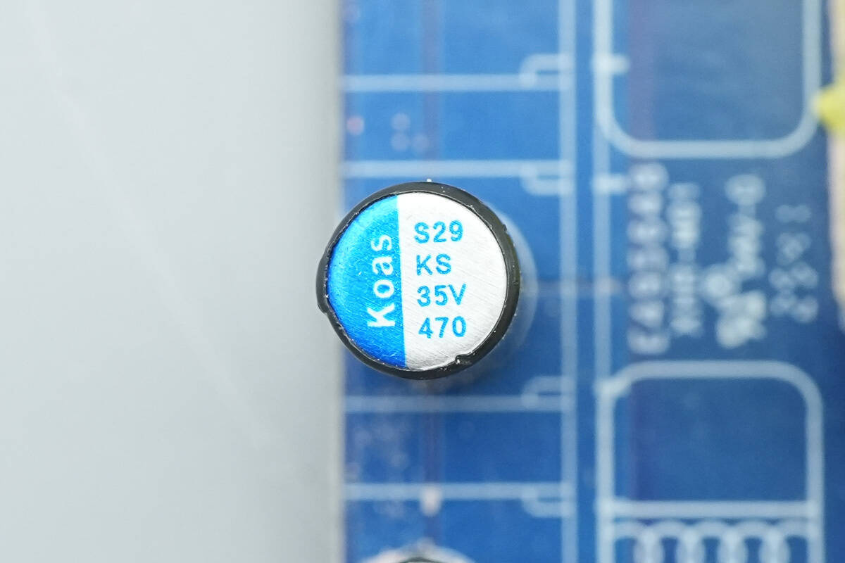
The filter capacitor is rated at 35 V, 470 μF.
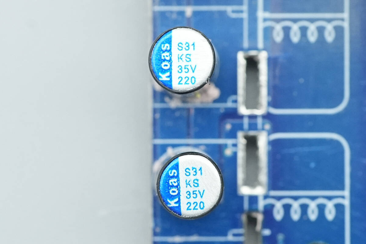
The other two filter capacitors are each rated at 35 V, 220 μF.
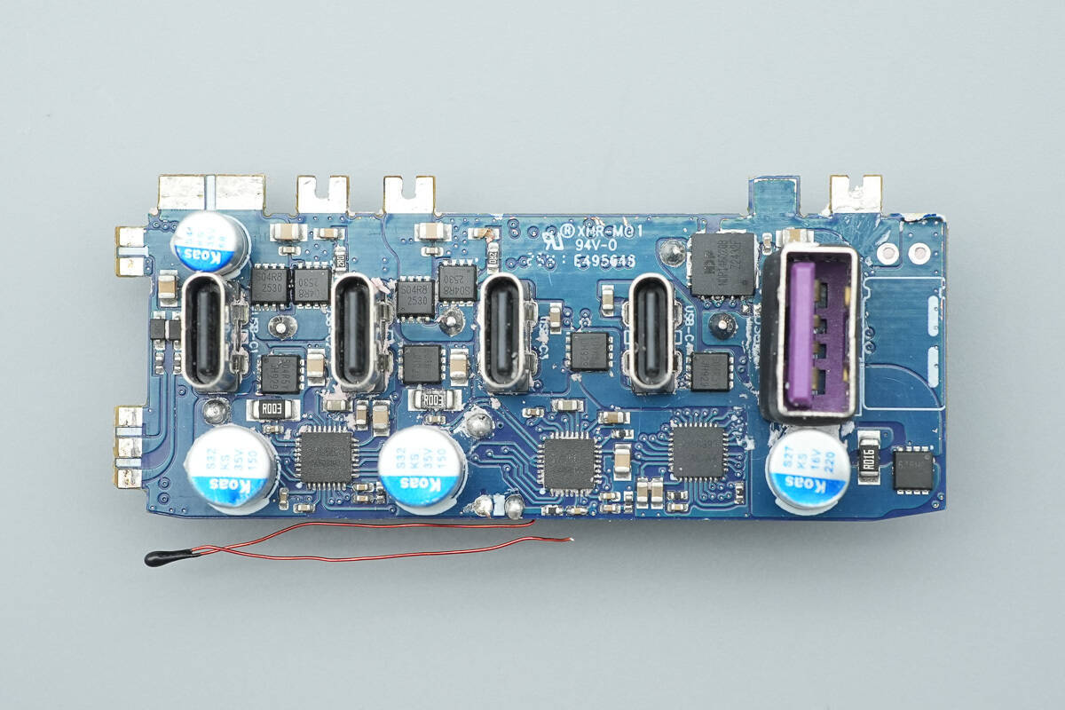
The front side of the buck PCB features buck protocol chips, synchronous buck MOSFETs, VBUS MOSFETs, a protocol chip, a synchronous buck controller, capacitors, and USB-C and USB-A connectors.
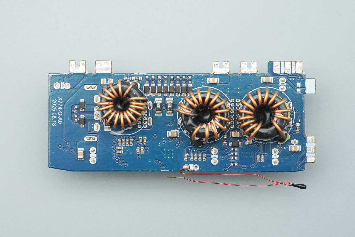
The back side has three buck inductors, each wound with enamel-coated wire.
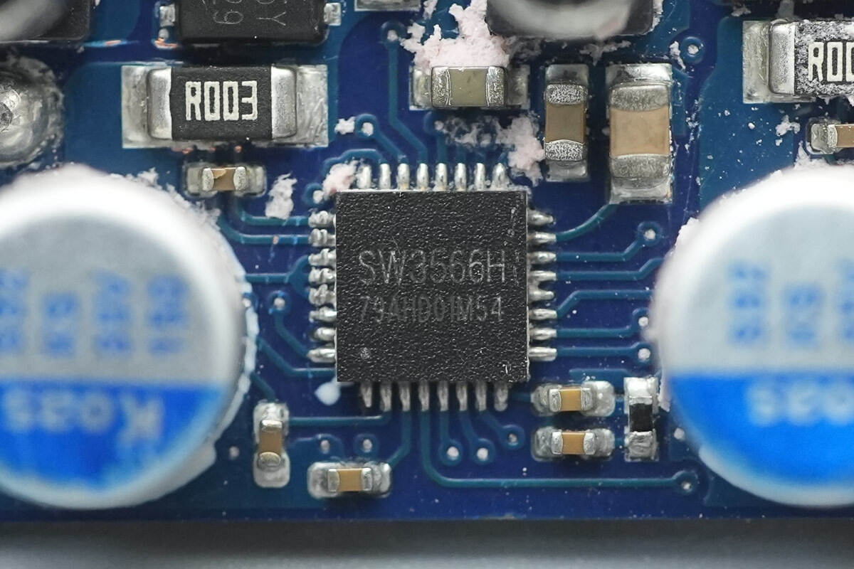
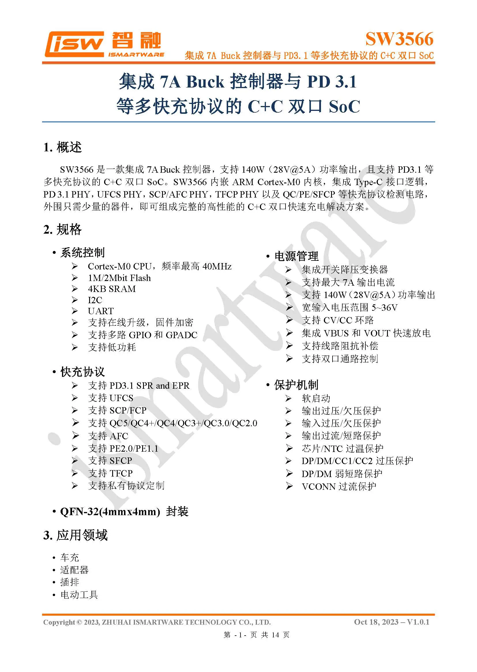
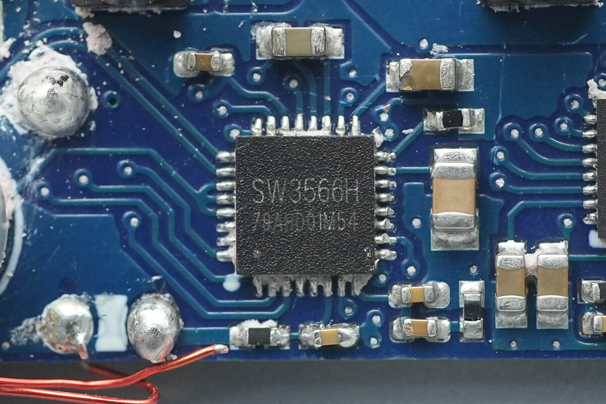
The USB-C1 port uses the iSmartWare SW3566H buck protocol chip, a highly integrated dual-port charging SoC supporting both USB-C and USB-A interfaces with independent dual-port current limiting. It integrates a high-efficiency synchronous buck converter, supporting 20 V/7 A and 28 V/5 A outputs, PD3.1/QC/SCP/UFCS fast-charging protocols, and customizable fast-charging protocols, with a maximum output power of 140 W.
The SW3566H integrates CC/CV mode, dual-port management logic, and bus voltage detection. Paired with the corresponding buck MOSFETs and VBUS MOSFETs, it enables dual-port buck output. The buck converter operates at 180 kHz and supports both PWM and PFM modes. Output current, line-loss compensation, and other protection thresholds can be configured via the I²C interface. Its built-in ADC provides nine-channel data sampling, including input/output voltage, output current, and chip temperature, supporting external MCU parameter display.
The SW3566H supports up to 36 V input and a maximum output current of 7 A. It features soft-start, input overvoltage/undervoltage protection, output overvoltage/undervoltage protection, output overcurrent/short-circuit protection, DP/DM/CC overvoltage protection, chip overheat protection, external NTC thermistor protection, and power-limiting protection. The package is QFN 4×4 mm, 32 pins.
Here is the information about iSmartWare SW3566.

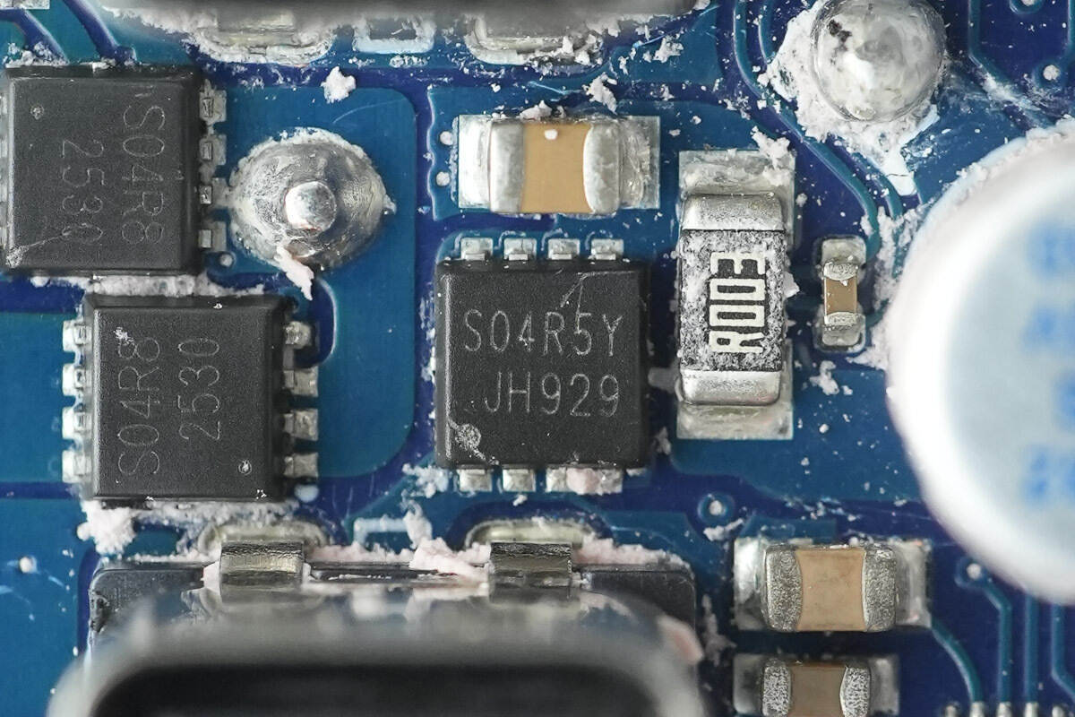
The synchronous buck MOSFETs are from Prisemi, marked S04R8, model PSM8PN04R8. They are NMOS devices rated at 40 V with an on-resistance of 6.1 mΩ, packaged in PDFN 3×3 mm, 8L.
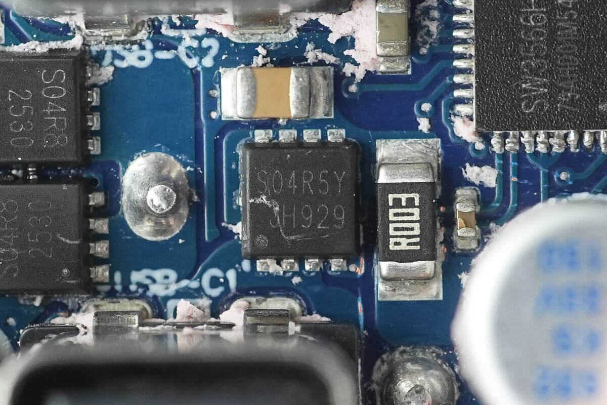
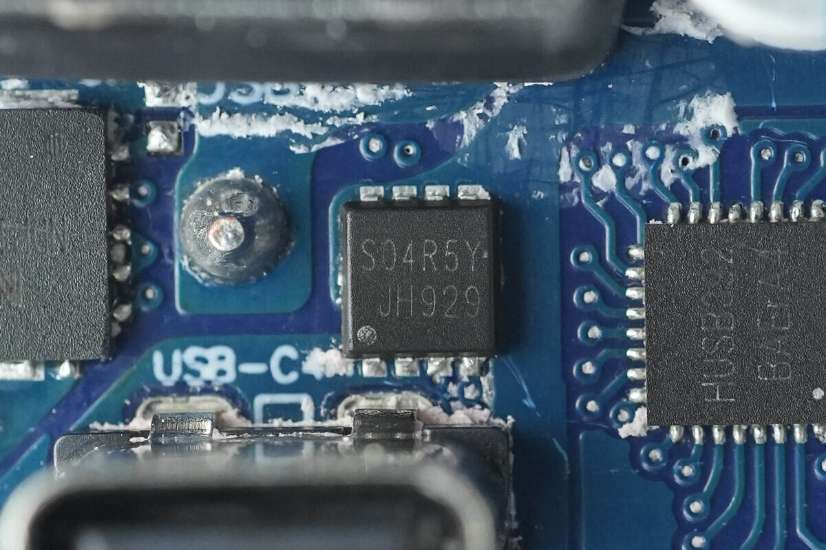
The VBUS MOSFET is from Prisemi, marked S04R5Y, model PSM8PN04R5. It is an NMOS device rated at 40 V with an on-resistance of 3.9 mΩ, packaged in PDFN 3×3 mm, 8L.
The USB-C2 port also uses the iSmartWare SW3566H buck protocol chip.
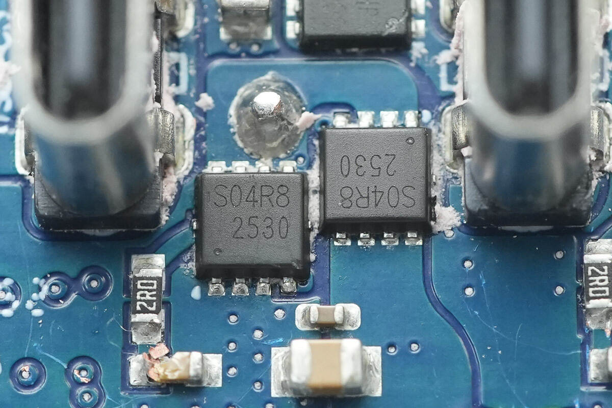
The synchronous buck MOSFETs for USB-C2 use the Prisemi PSM8PN04R8.
The VBUS MOSFET for USB-C2 uses the Prisemi PSM8PN04R5.
The input filter capacitor is rated at 35 V, 68 μF.
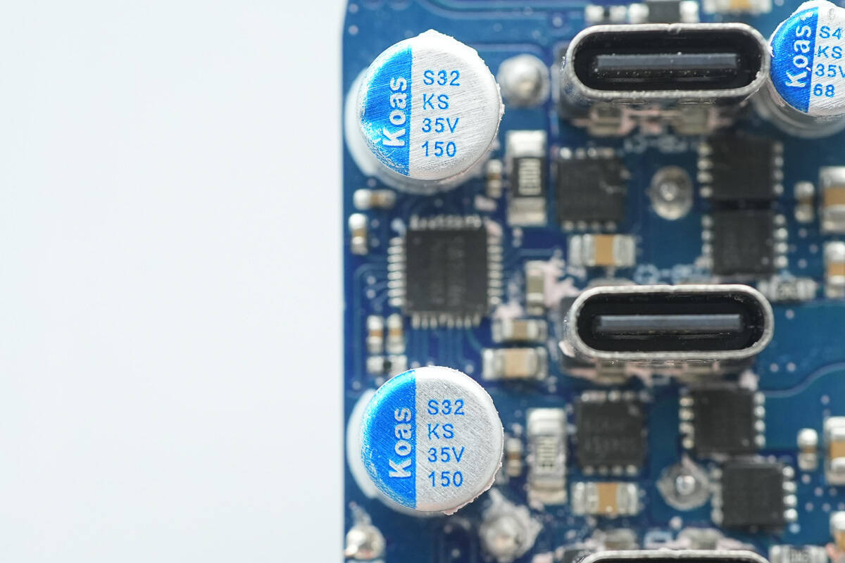
The two output filter capacitors are each rated at 35 V, 150 μF.
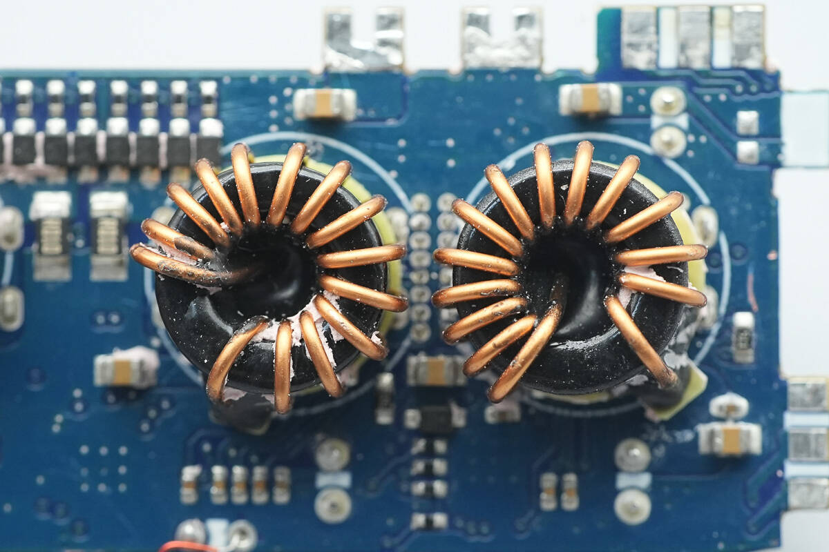
The buck inductors are wound with enamel-coated wire and have bakelite insulating bases.
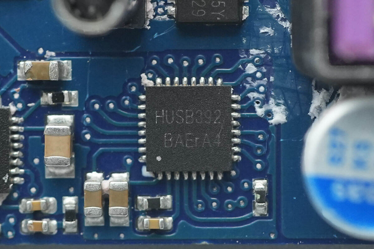
The protocol chip for the USB-C3, USB-C4, and USB-A ports is the Hynetek HUSB392, a high-performance, highly integrated 3-port controller supporting 18–65 W in 2C1A or 2A1C multi-port configurations. It supports PD3.1 fast charging; when a single port is used, fast charging output is available, while connecting two or three ports fixes the output voltage at 5 V.
The HUSB392 features an I²C interface for reading output voltage, output current, port current, and protocol status, and allows power-limit settings via I²C. It integrates protection functions including overvoltage protection, undervoltage protection, undervoltage lockout, overcurrent protection, short-circuit protection, and thermal protection. The package is QFN-32L.
Here is the information about Hynetek HUSB392.
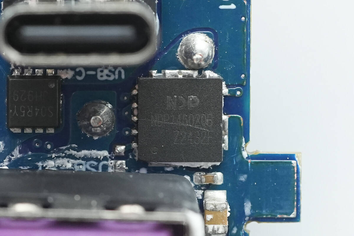
The synchronous buck converter is from NDP, model NDP14602QB. It integrates internal MOSFETs, supports 7.5–37 V input voltage, 6 A output current, adjustable line compensation, and dual-channel constant-voltage/constant-current control. The package is QFN 5×5 mm.
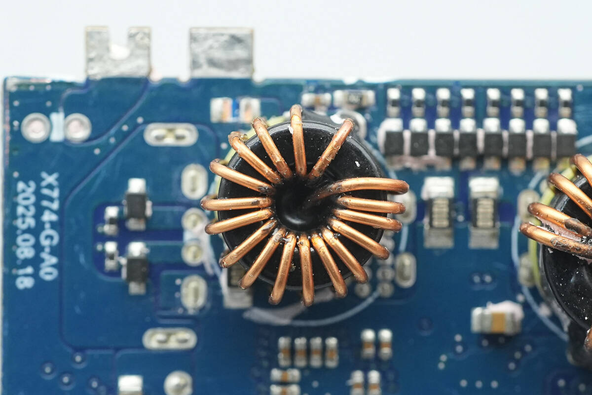
The buck inductor is wound with enamel-coated wire.
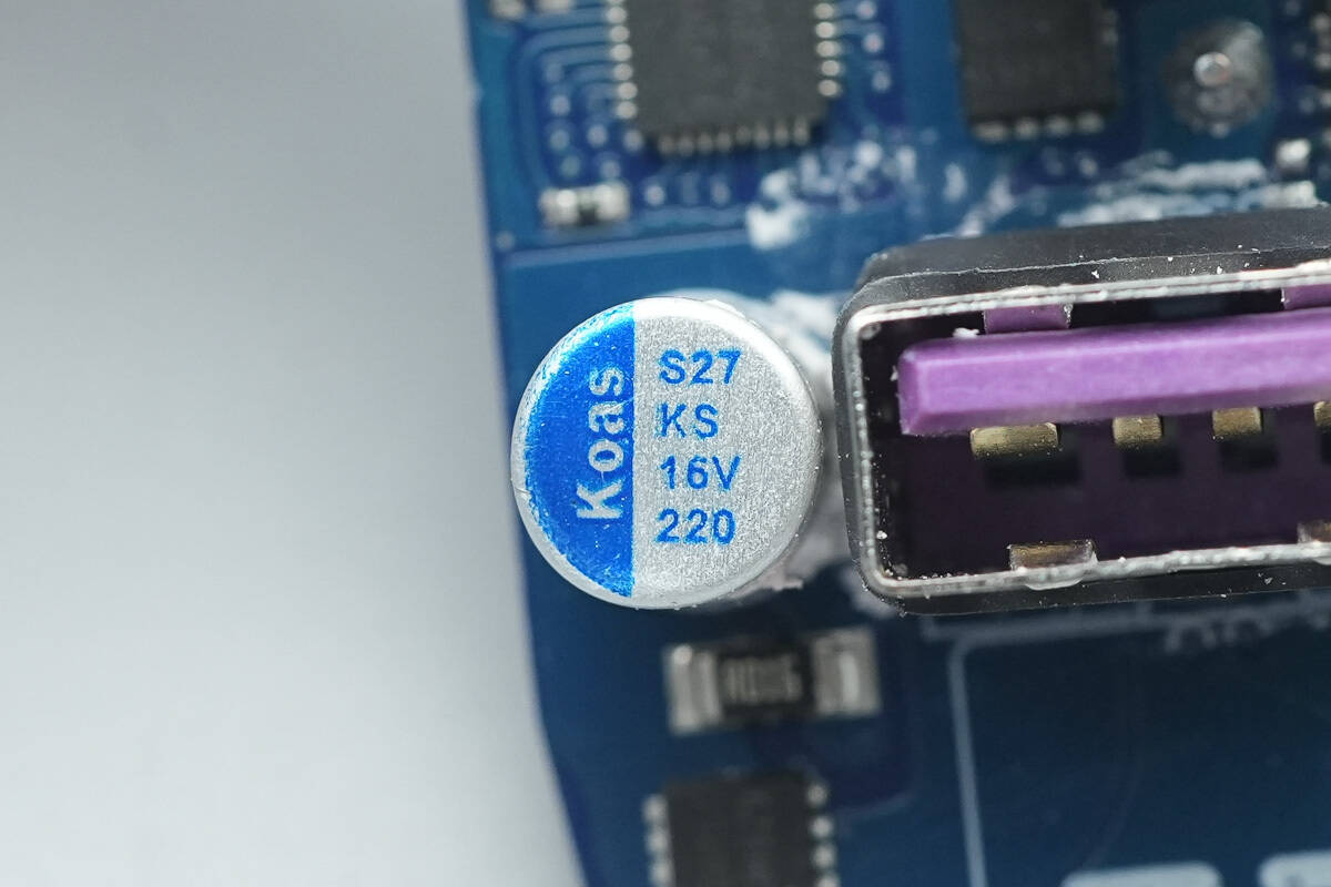
The filter capacitor is rated at 16 V, 220 μF.

The USB-C3 port VBUS MOSFET uses the Prisemi PSM8PN04R5.
The USB-C4 port VBUS MOSFET uses the Prisemi PSM8PN04R5.

The USB-A port VBUS MOSFET uses the Prisemi PSM8PN04R5.

The USB-C ports are fixed using through-hole soldering.
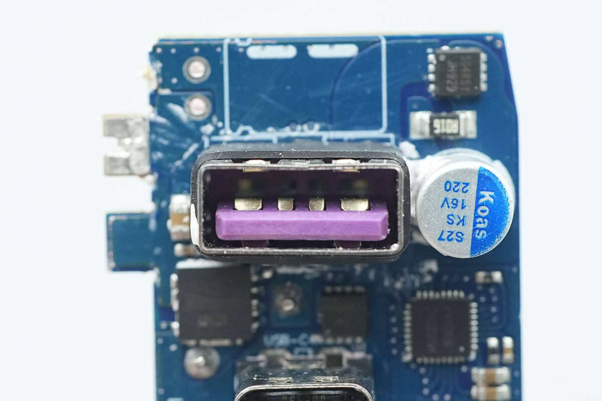
The USB-A port uses a purple plastic sheet.
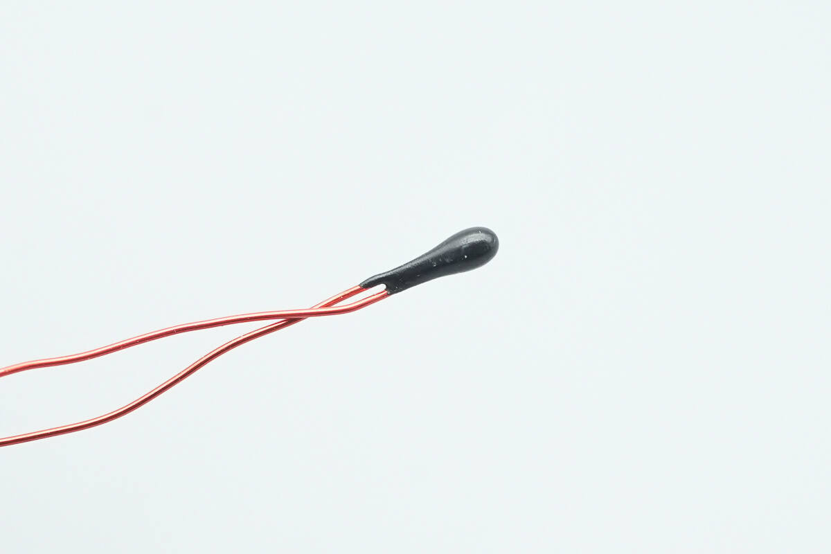
The thermistor is used to monitor the internal temperature of the charger.
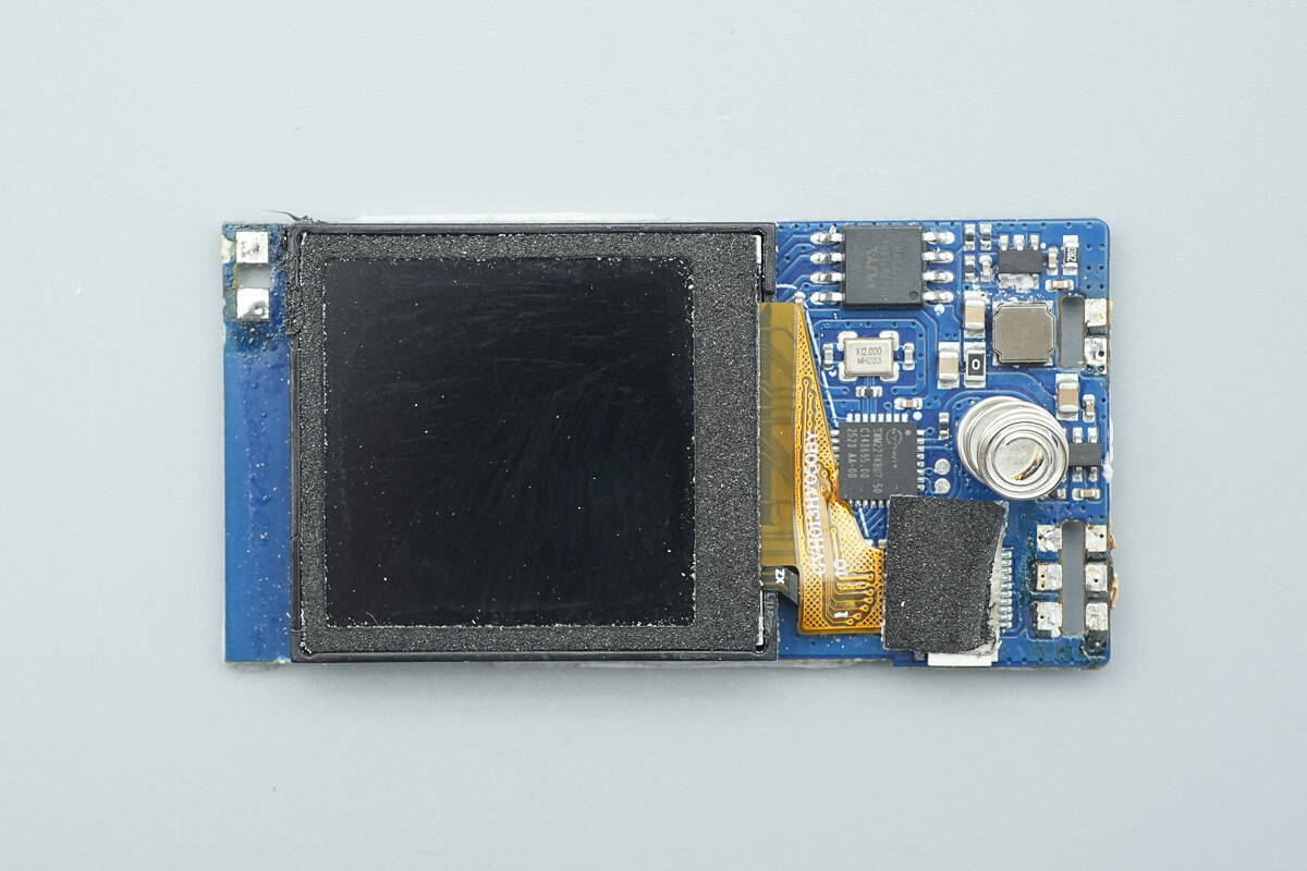
The front side of this PCB features the screen, MCU, memory, touch detection chip, and buck converter chip.
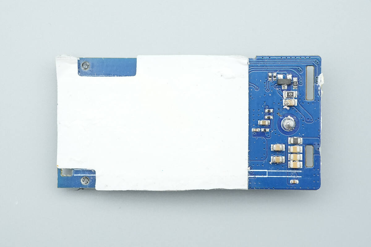
The other side is covered with a cushioning foam pad.
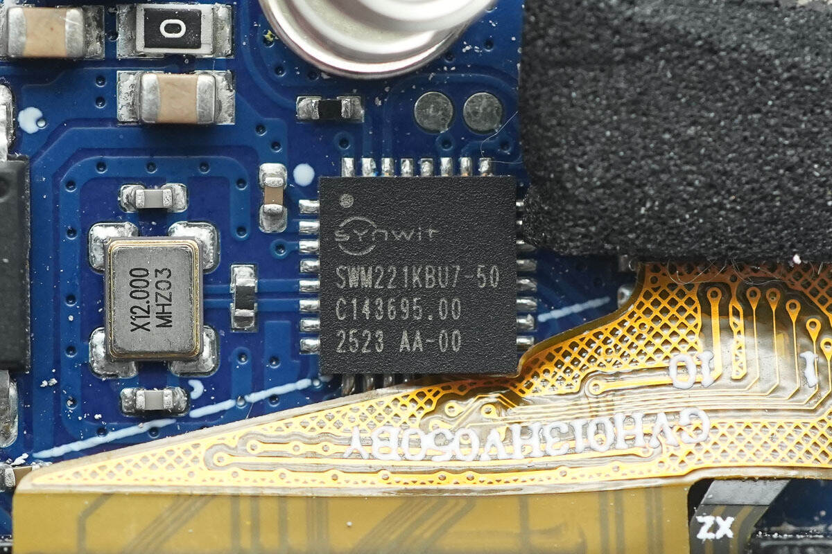
The MCU used for screen driving is from Synwit, model SWM221KBU7-50. It integrates a 32-bit ARM Cortex-M0 core with a 72 MHz clock, supports a 2.2–5.5 V operating voltage, and includes 128 KB of FLASH and 8 KB of SRAM. It features UART, USART, I²C, SPI, and QSPI interfaces, and comes in a QFN32 package.

Close-up of the 12.000 MHz SMD crystal oscillator.

The memory is from Puya, model PY25Q128HA, with a capacity of 128 MB, supporting a 2.7–3.6 V operating voltage, and comes in an SOP8 package.

The buck converter chip is from Techcode, model TD1469. It is a synchronous buck converter with a 7–40 V input voltage range, built-in MOSFETs, a 1.2 MHz switching frequency, and an 800 mA output current. It features overheat and overcurrent protection and comes in a SOT-23-6 package.
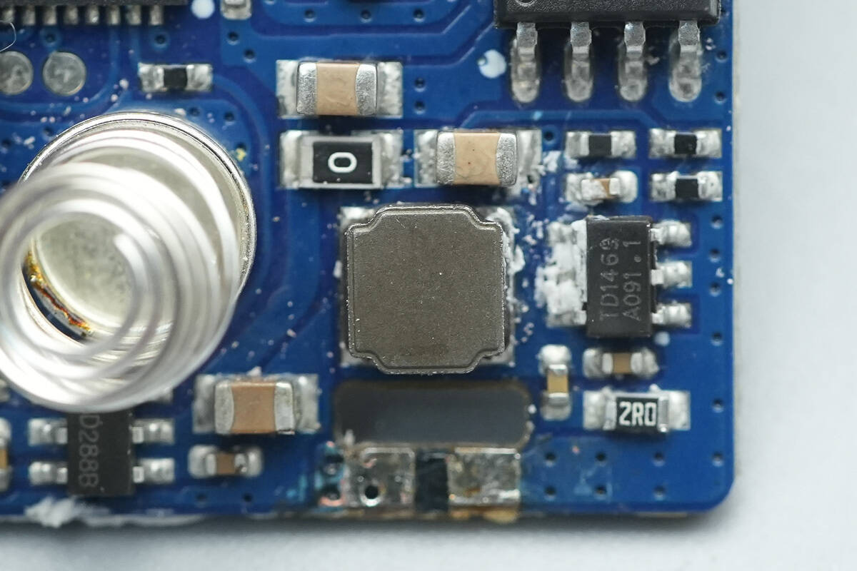
Close-up of the buck inductor.
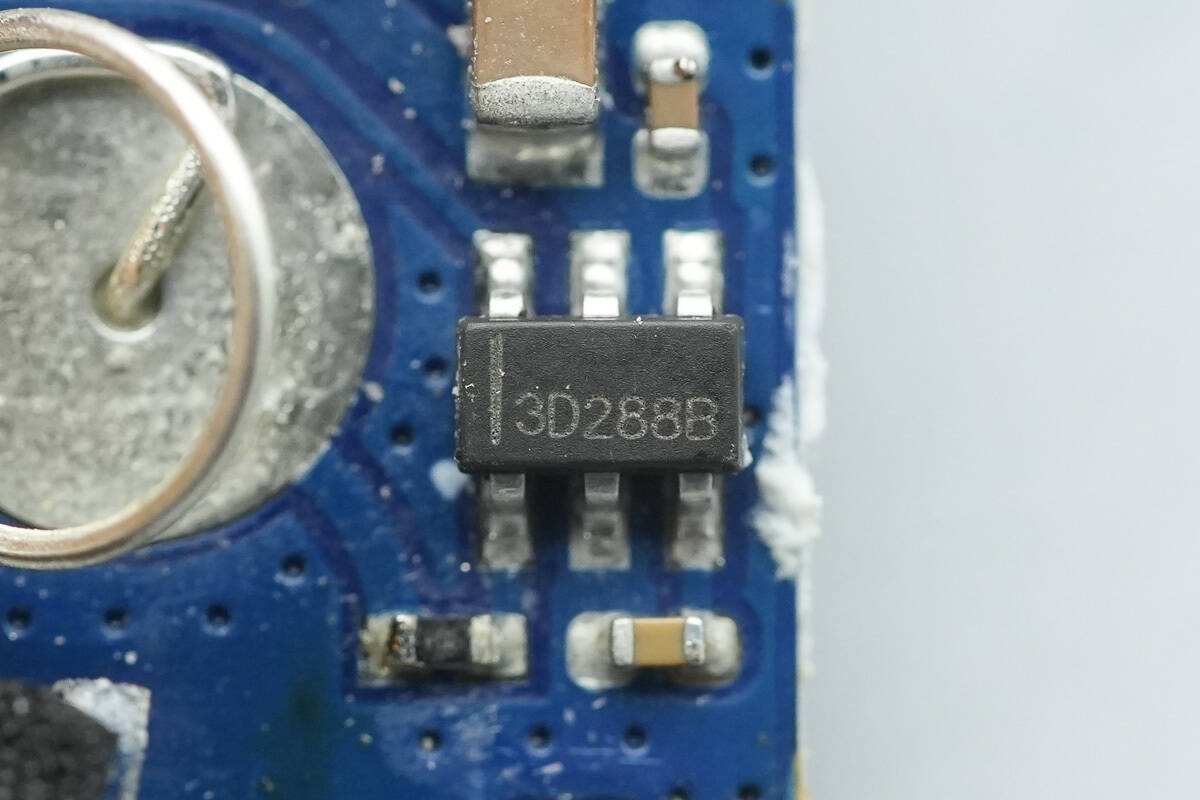
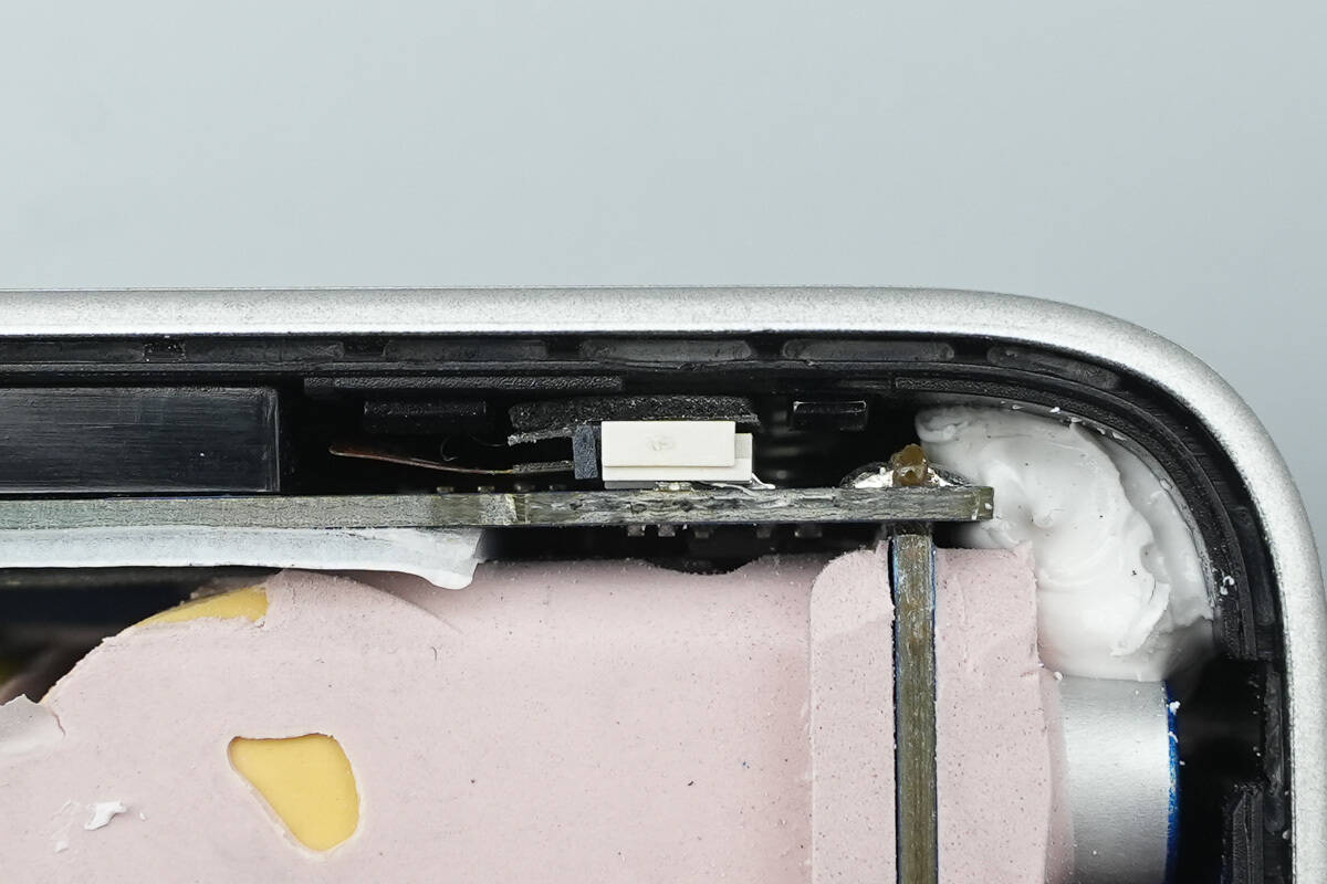
The touch controller is marked 3D288B and comes in a SOT-23 package.
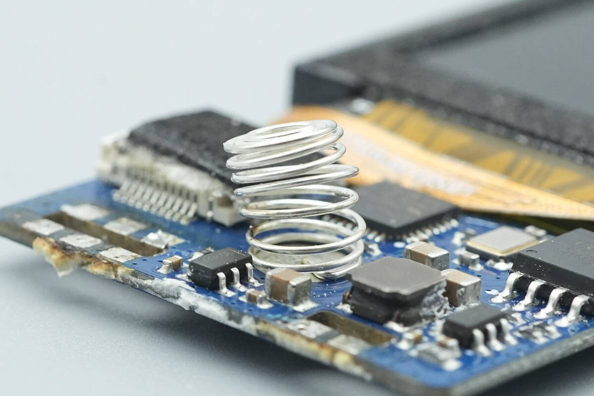
Close-up of the touch spring.
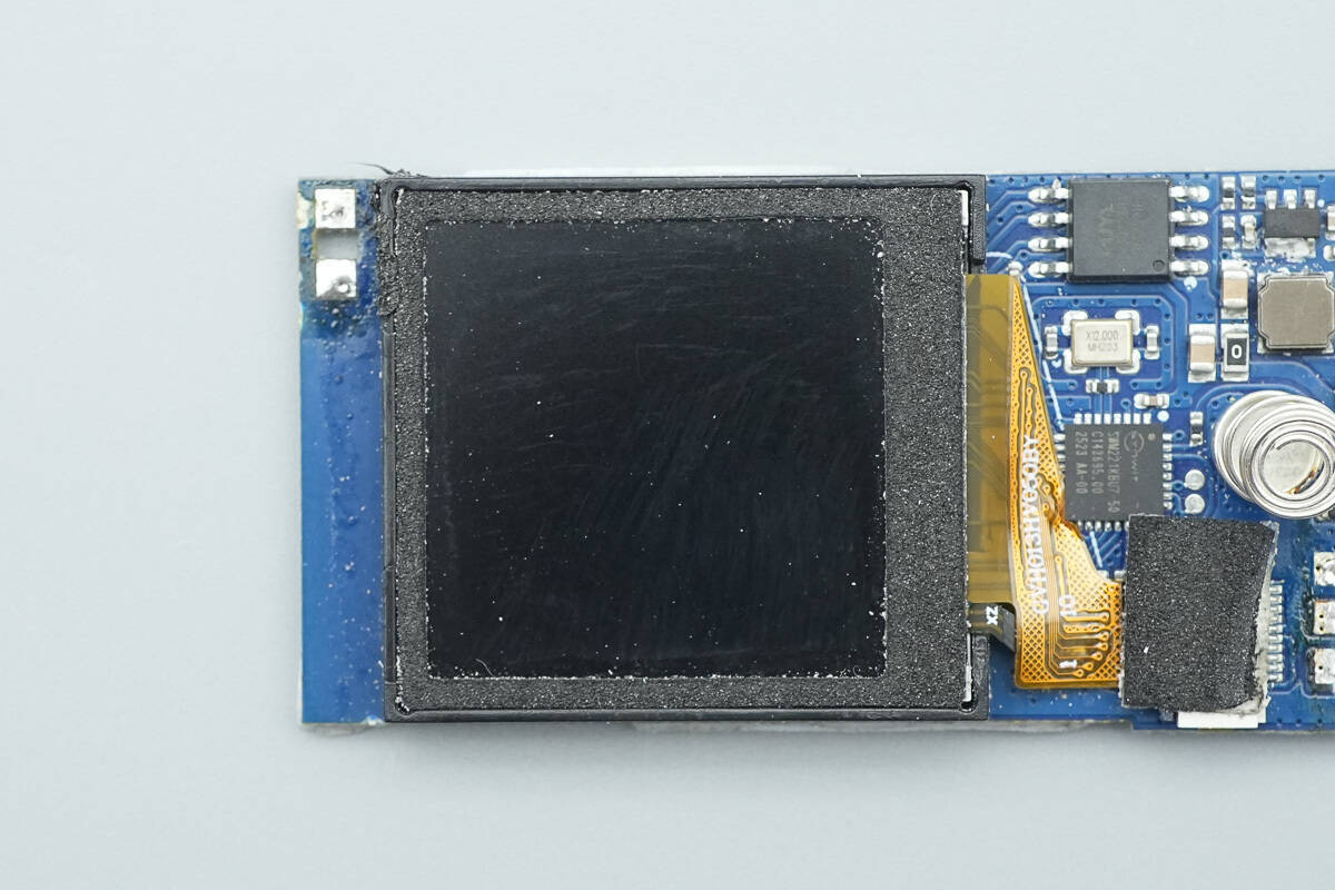
Sealing foam is applied along the edges of the screen.

The screen is connected via a flexible flat cable.
Well, those are all components of the UGREEN Nexode 160W 5-Port GaN Charger.
Summary of ChargerLAB
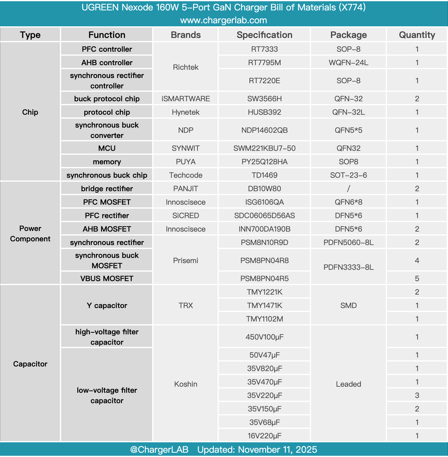
Here is the component list of the UGREEN Nexode 160W 5-Port GaN Charger for your convenience.
Its LCD screen can be controlled via touch buttons and displays total output power, multi-port power distribution, and charging protocols. The charger features four USB-C ports and one USB-A port, with a total output of 160W. Two of the USB-C ports support 140W PD 3.1.
After taking it apart, we found that the PCBA module is composed of multiple small PCBs soldered together. The power supply uses a PFC + AHB + synchronous rectification architecture. The switching power solution comes from RICHTEK, using an RT7333 PFC controller paired with an RT7795M AHB controller and an RT7220E synchronous rectifier controller.
The PFC MOSFET is Innoscience ISG6106QA, paired with a SiCRED SDC06065D56AS PFC rectifier. The AHB MOSFETs are Innoscience INN700DA190B, and the synchronous rectifiers are Prisemi PSM8N10R9D.
The buck protocol chips for the USB-C1 and C2 ports use iSmartWare SW3566H, while the USB-C3 port uses the Hynetek HUSB392 protocol chip, paired with the NDP NDP14602QB synchronous buck converter. The high-voltage filter capacitor and solid capacitors are all from Koshin. The PCBA module is encapsulated with high-performance thermal adhesive, enhancing heat dissipation and reliability. The workmanship and component selection are solid and dependable.
Related Articles:
1. Teardown of Xiaomi 67W 20000mAh Power Bank with Integrated Cable (PB2067)
2. Teardown of HONOR 80W SuperCharge Wireless Charger Stand (Power-W06)
3. Teardown of Infypower 40kW EV SiC Power Module (REG1K0135A2)