
Introduction
Xiaomi made waves late last year with the Xiaomi Ultra Slim Power Bank 5000mAh, a device that highlights the company’s focus on advanced battery chemistry. Featuring the proprietary Jinshajiang tech, this slim unit manages to deliver 5000mAh of power without the bulk. With 15W wireless magnetic charging and 22.5W wired output, it’s a versatile tool for daily use. ChargerLAB has already put the hardware through its paces, covering both real-world performance testing and a detailed internal teardown.
Innovation in the charging space is now being met with stricter oversight. As of March 31, 2026, the new "Mobile Power Supply Safety Technical Specification" has officially taken effect. This updated 3C Chinese standard marks a significant milestone in safety compliance, setting a rigorous new baseline for the entire mobile charging industry.
Manufacturers are now tasked with ensuring that their designs not only excel in efficiency but also meet these stringent, newly implemented safety protocols.
Xiaomi is leading the charge under the new regulations. Their latest release, the Xiaomi Ultra Slim Power Bank 10,000mAh 45W, perfectly blends high-capacity performance with sleek, family-consistent aesthetics. With a sturdy, silver aluminum body and refined curved edges, it is designed for both durability and comfort.
Xiaomi has achieved an impressive feat of engineering here: 10,000mAh of capacity packed into a frame just 13.20mm thin and weighing only 196.3g. This is a game-changer for magnetic chargers. More importantly, it is "regulation-ready," offering real-time health tracking via Xiaomi’s official web portal. With 45W wired charging—supporting HyperCharge, PD 3.2, and PPS—and a 20W wireless output, it covers all the bases for a modern mobile workflow.
We’re taking this apart today to see exactly what’s driving this performance inside.
Product Appearance
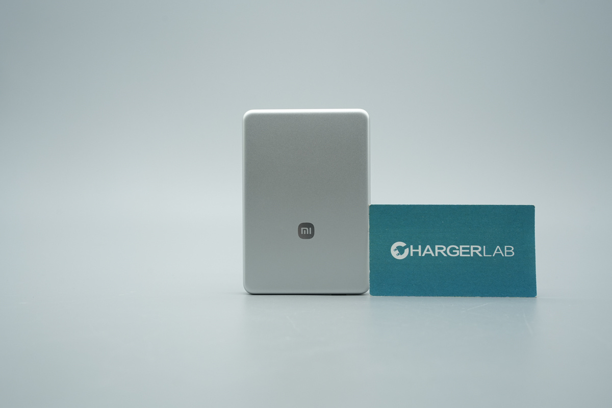
The power bank is enclosed in a durable unibody silver aluminum alloy shell, featuring a smooth, high-quality finish and the Xiaomi logo.
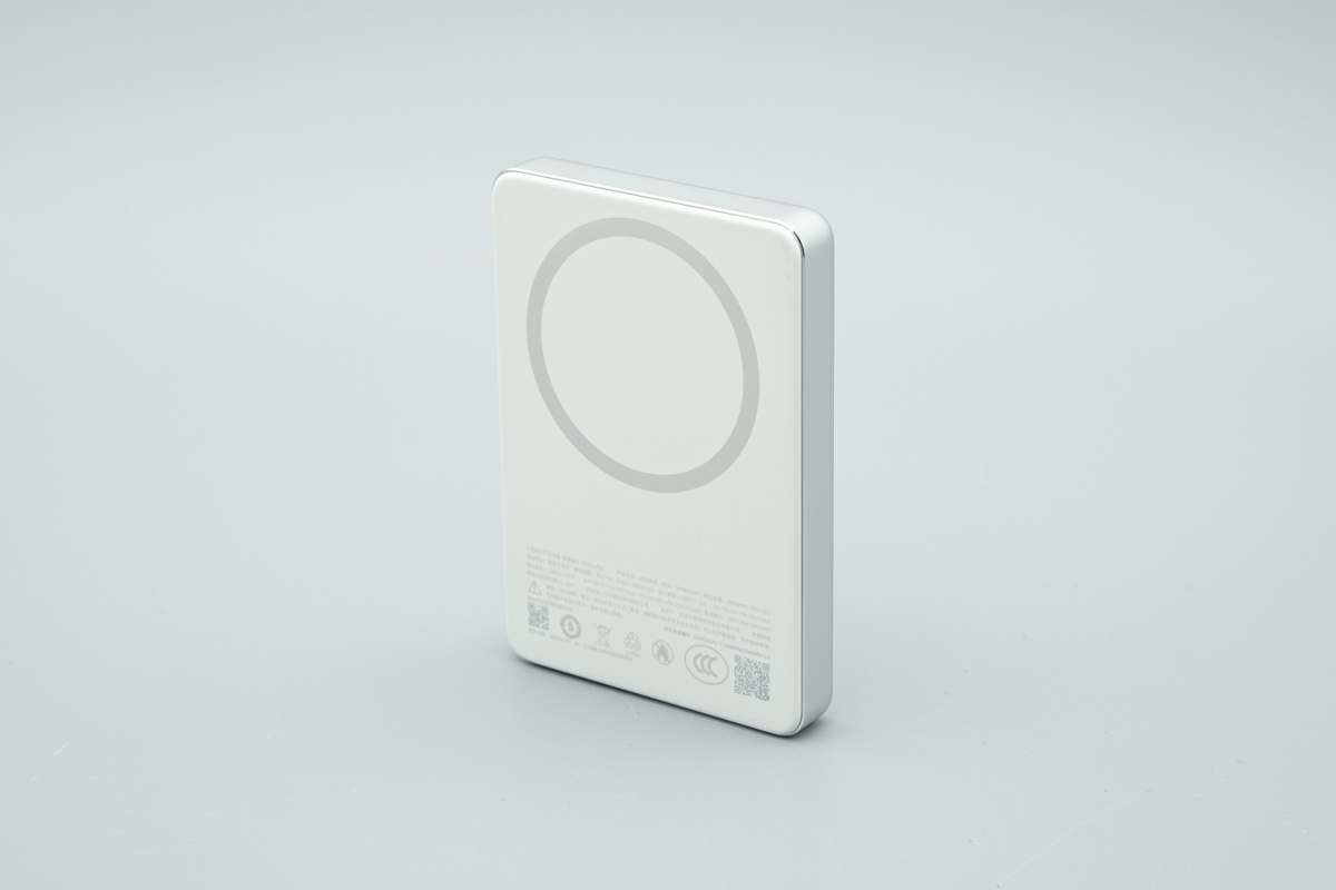
The back of the power bank features a minimalist design with a centered circular ring to indicate the magnetic wireless charging area.
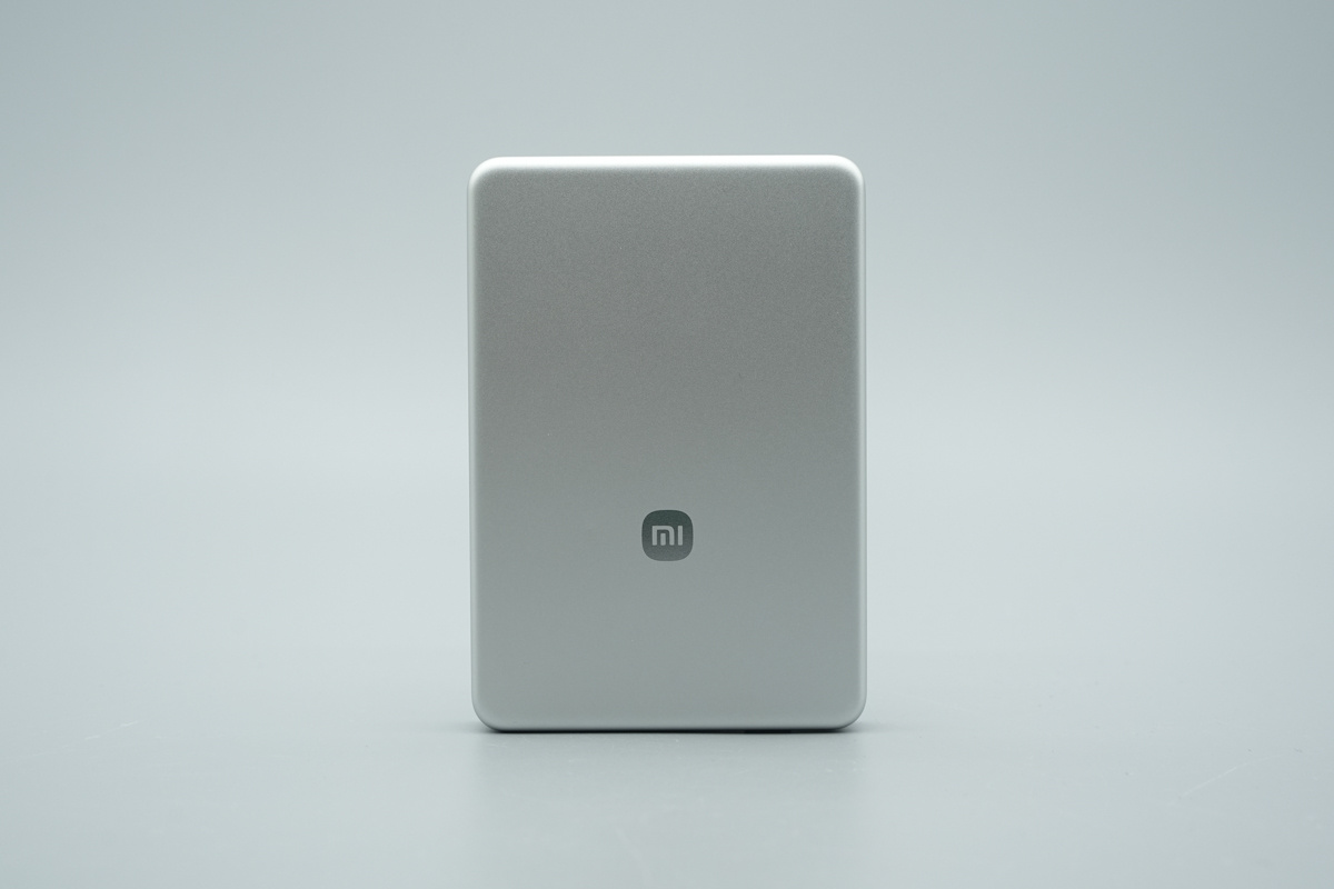
The front housing utilizes large-radius curved edges to create a rounded profile. The overall design is consistent with the family aesthetic established by the previously reviewed Xiaomi Ultra Slim Power Bank 5000mAh.
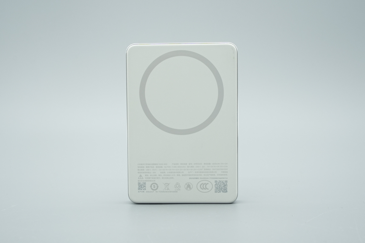
The product's detailed specs and parameters are printed at the bottom of the back panel.
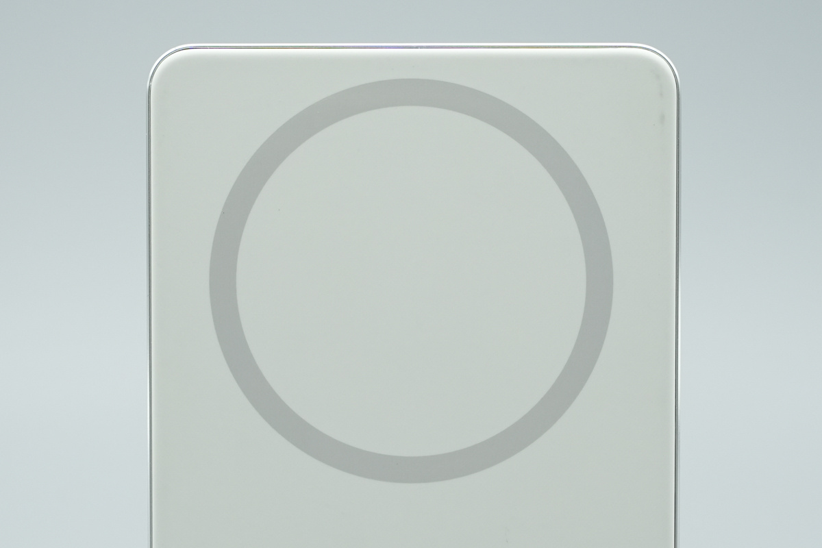
The magnetic charging area is precisely calibrated to snap onto your device effortlessly. It provides a seamless, "snap-and-go" experience.
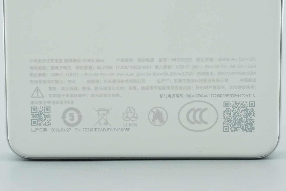
Product Specs:
Model: WPB1025S
Capacity: 5800mAh (5V3A)
Battery: Lithium-Ion
Energy: 36.77Wh (7.58V/4,850mAh)
USB-C Input: 5V/3A, 9V/3A, 12V/2.5A
USB-C Output: 5V/3A, 9V/3A, 11V/4.1A, 12V/3A, 15V/3A, 20V/2.25A
Wireless Output: 5W, 7.5W, 15W, 20W
Dual Output: 15W
Certification: Chinese 3C Certified
Manufacturer: Xiaomi Communications Co., Ltd.
Factory: Dongguan Aohai Technology Co., Ltd. (Made in China)
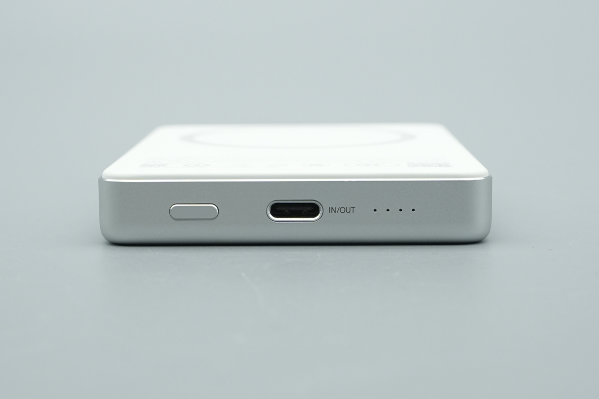
This is the bottom interface panel, from left to right, it includes the power button, a bidirectional USB-C fast-charging port, and four LED battery indicators.
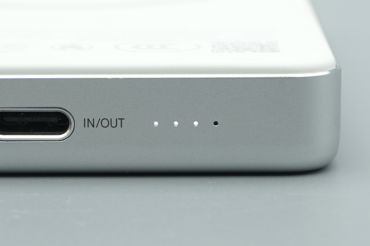
The USB-C port is labeled "IN/OUT," while four LED battery indicators are positioned to its right to display battery levels.
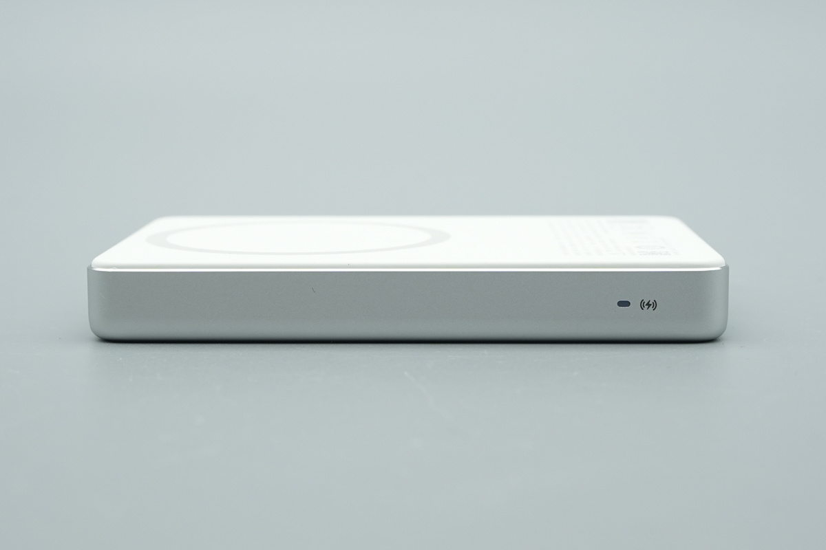
A wireless charging status indicator is located on the side.
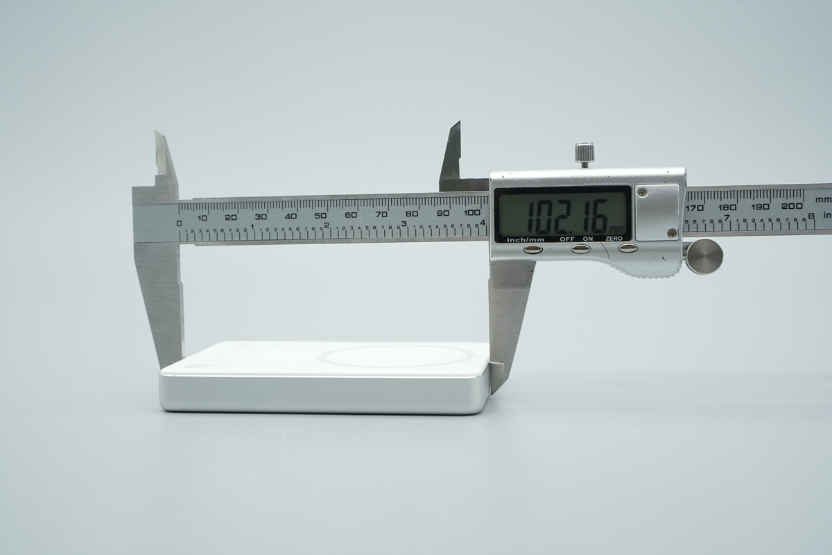
The length of the power bank is about 102.16mm (4.022 inches).
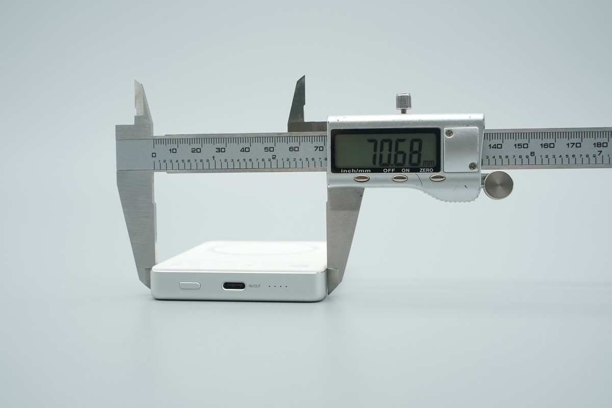
The width of the power bank is about 70.68mm (2.783 inches).
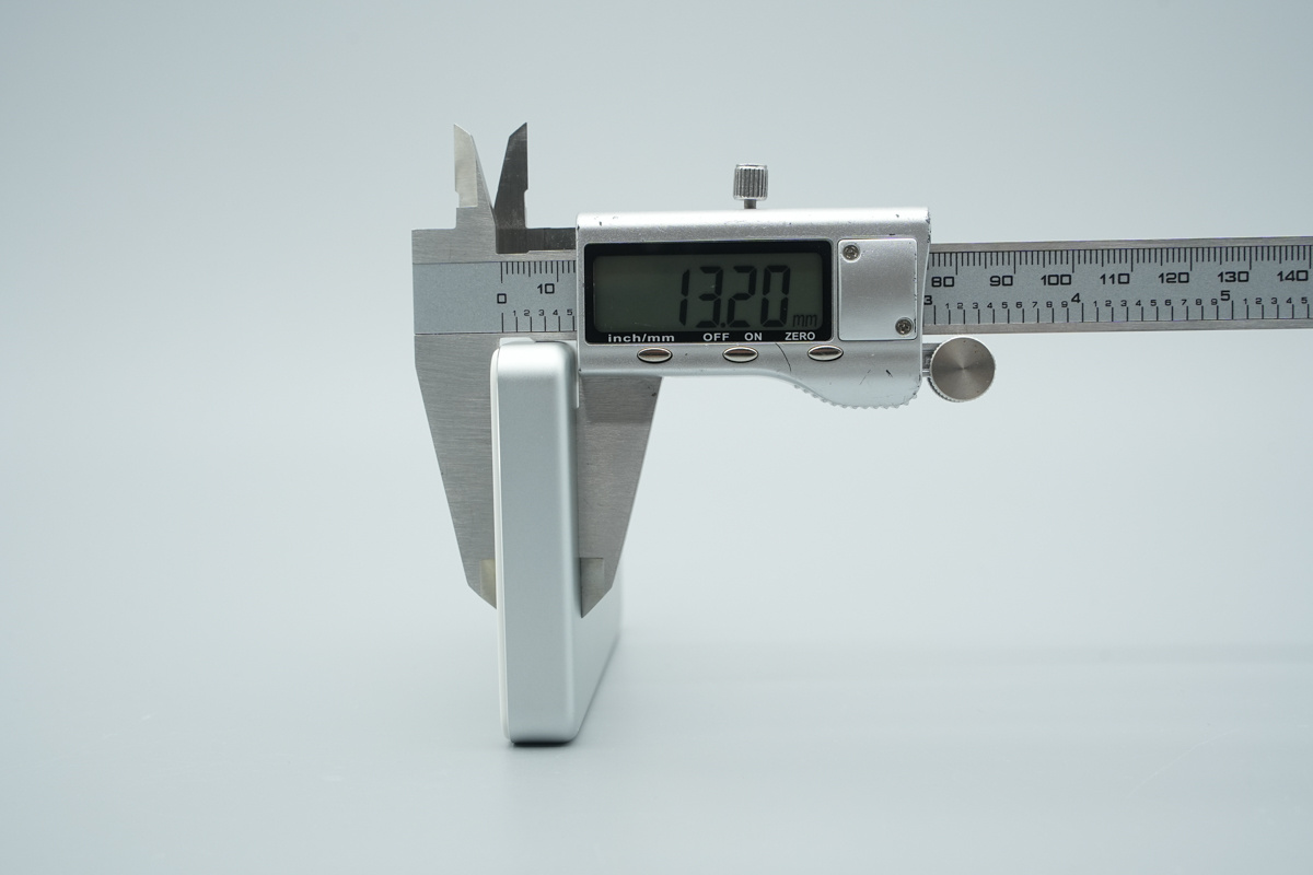
The thickness of the power bank is about 13.20mm (0.520 inches).
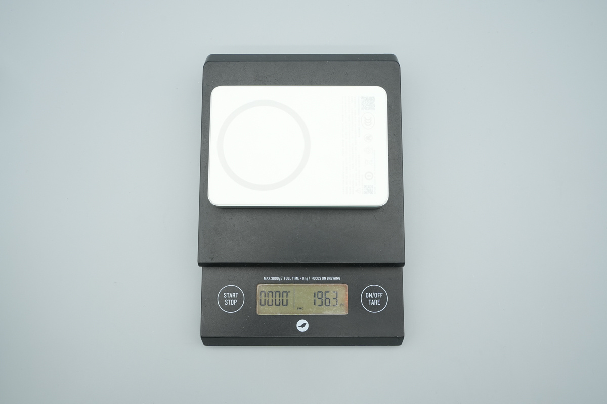
The weight is about 196.3g (6.92 oz).
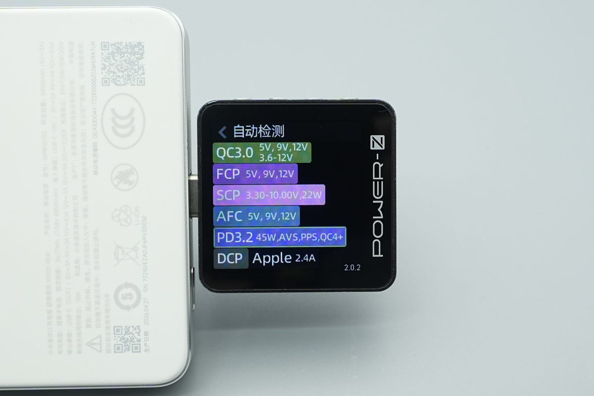
ChargerLAB POWER-Z KM003C shows that the USB-C1 port supports QC3.0, FCP, SCP, AFC, PD3.2/PPS, QC4+, DCP and Apple 2.4A.
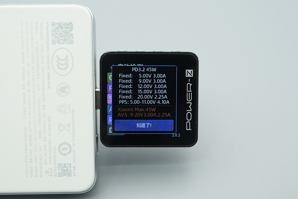
And it also supports five fixed PDOs of 5V3A, 9V3A, 12V3A, 15V3A and 20V2.25, features 5-11V/4.1A PPS subset and 9-20V/2.25A Xiaomi fast-charging subset.
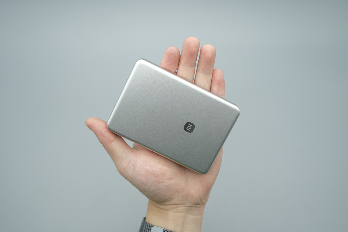
That's how big it is in the hand.
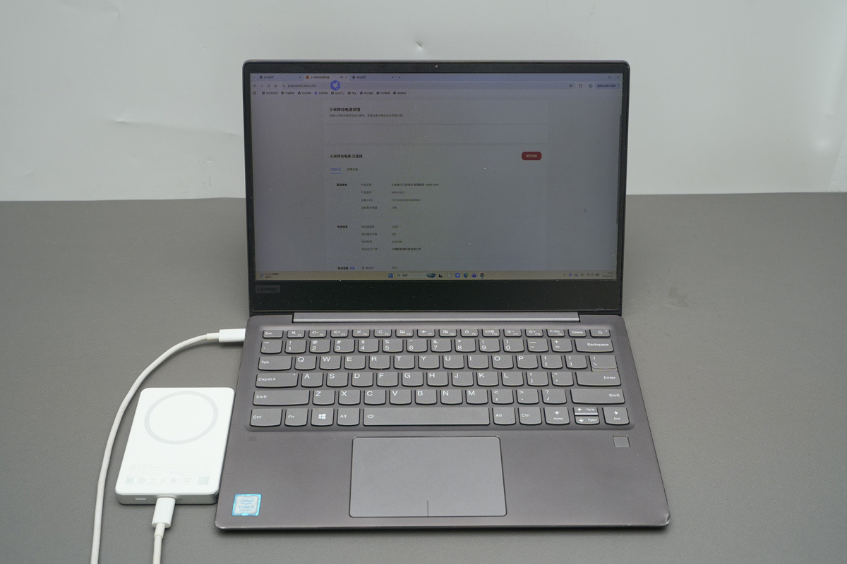
By connecting it to a laptop, we can view detailed device info via Xiaomi's official website, which shows it complies with the latest 3C Chinese safety standards.
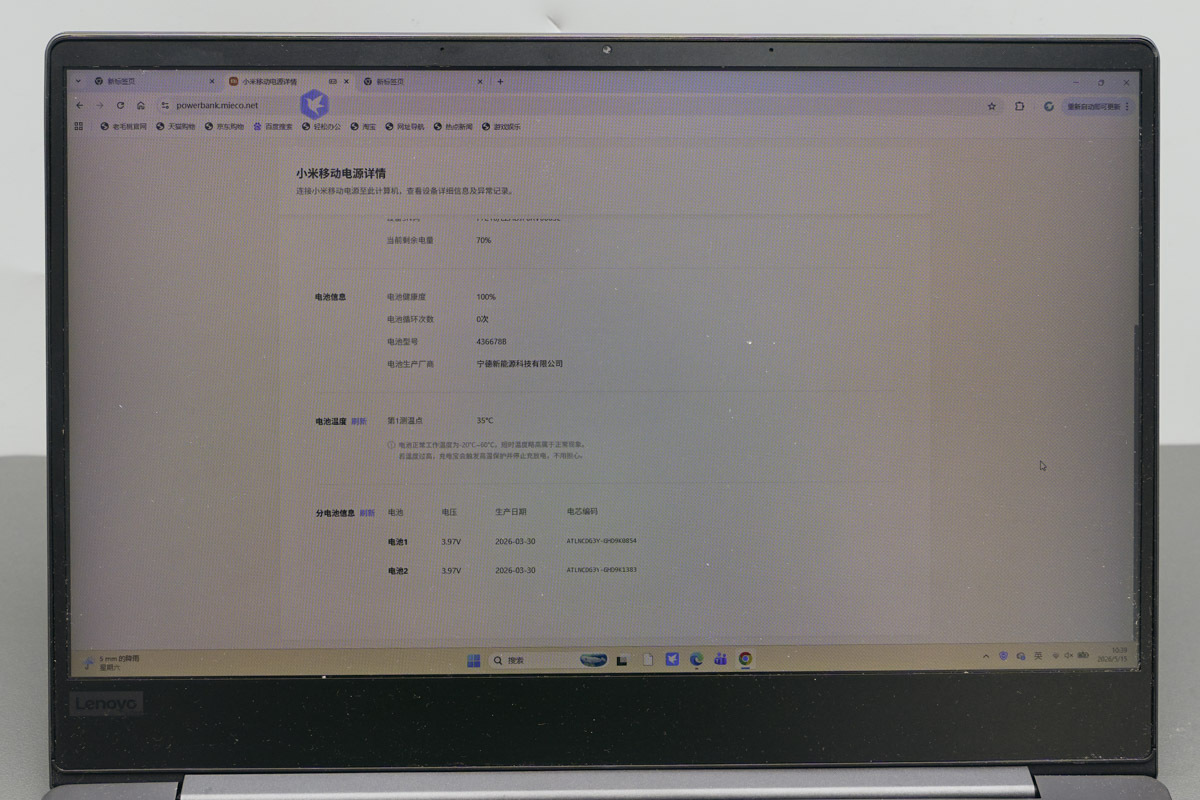
After connecting, the interface provides intuitive access to base device and battery info. It reveals a two-series cell architecture and allows for real-time monitoring of individual cell voltages and internal temperature.
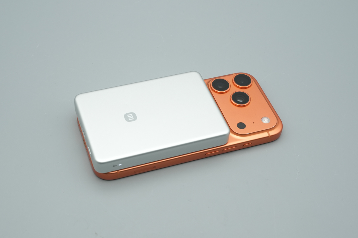
We’ve attached it to an iPhone 17 Pro.
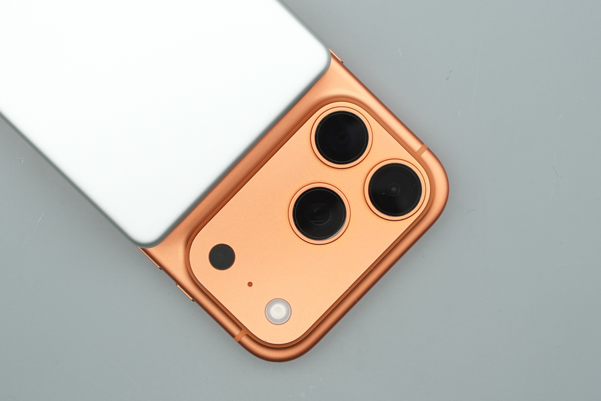
Once attached, there is plenty of clearance, ensuring it stays well away from the camera.
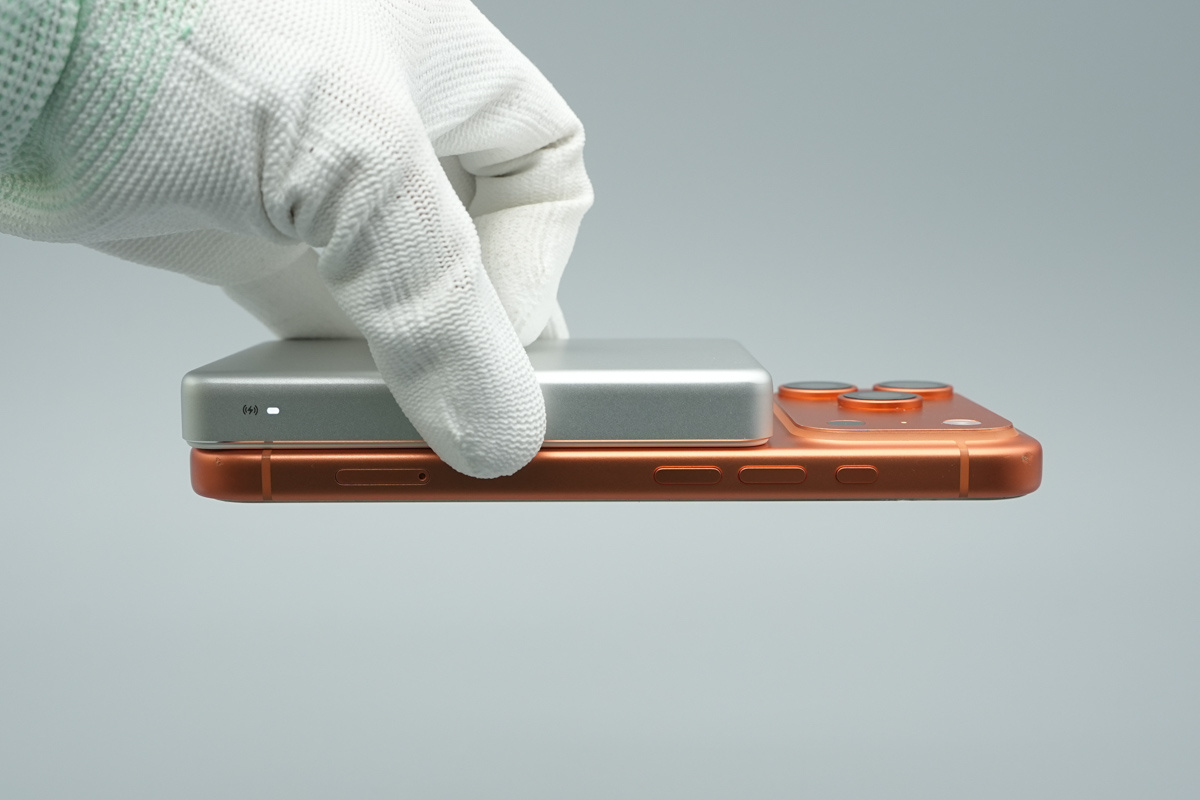
The magnetic connection is strong enough to hold the smartphone securely even when it is held with one hand, ensuring it stays firmly in place without detaching.
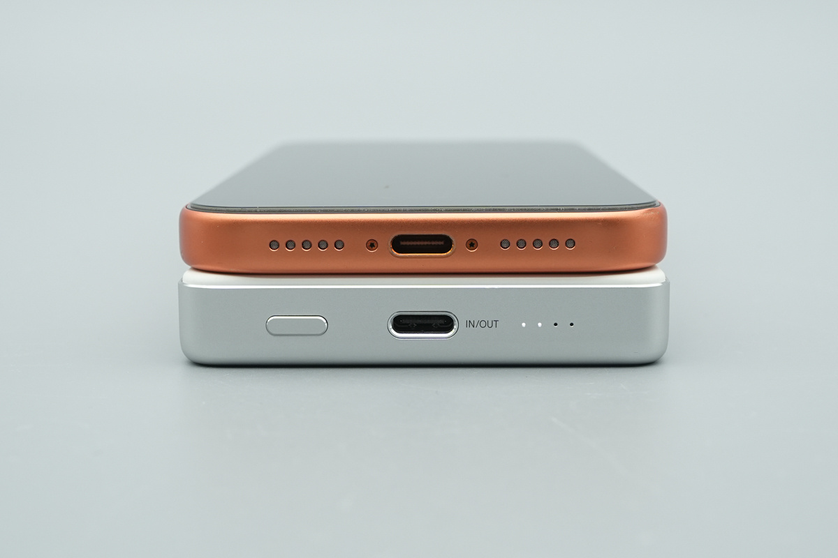
When attached, the USB-C ports of the power bank and the iPhone align perfectly, resulting in a neat and visually appealing appearance.
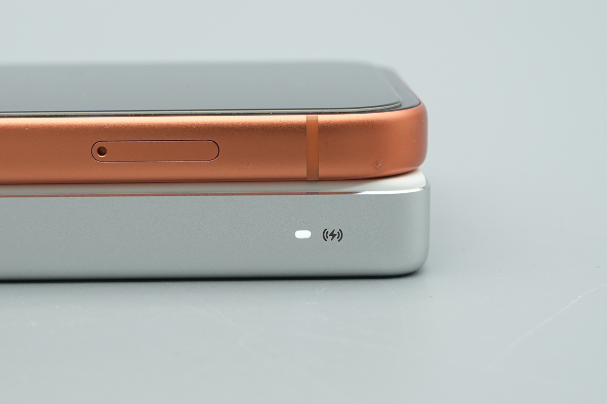
The side indicator glows white while wirelessly charging the iPhone.
After a quick look at the design and functional test, it’s time for us to dive into the teardown here at ChargerLAB.
Teardown
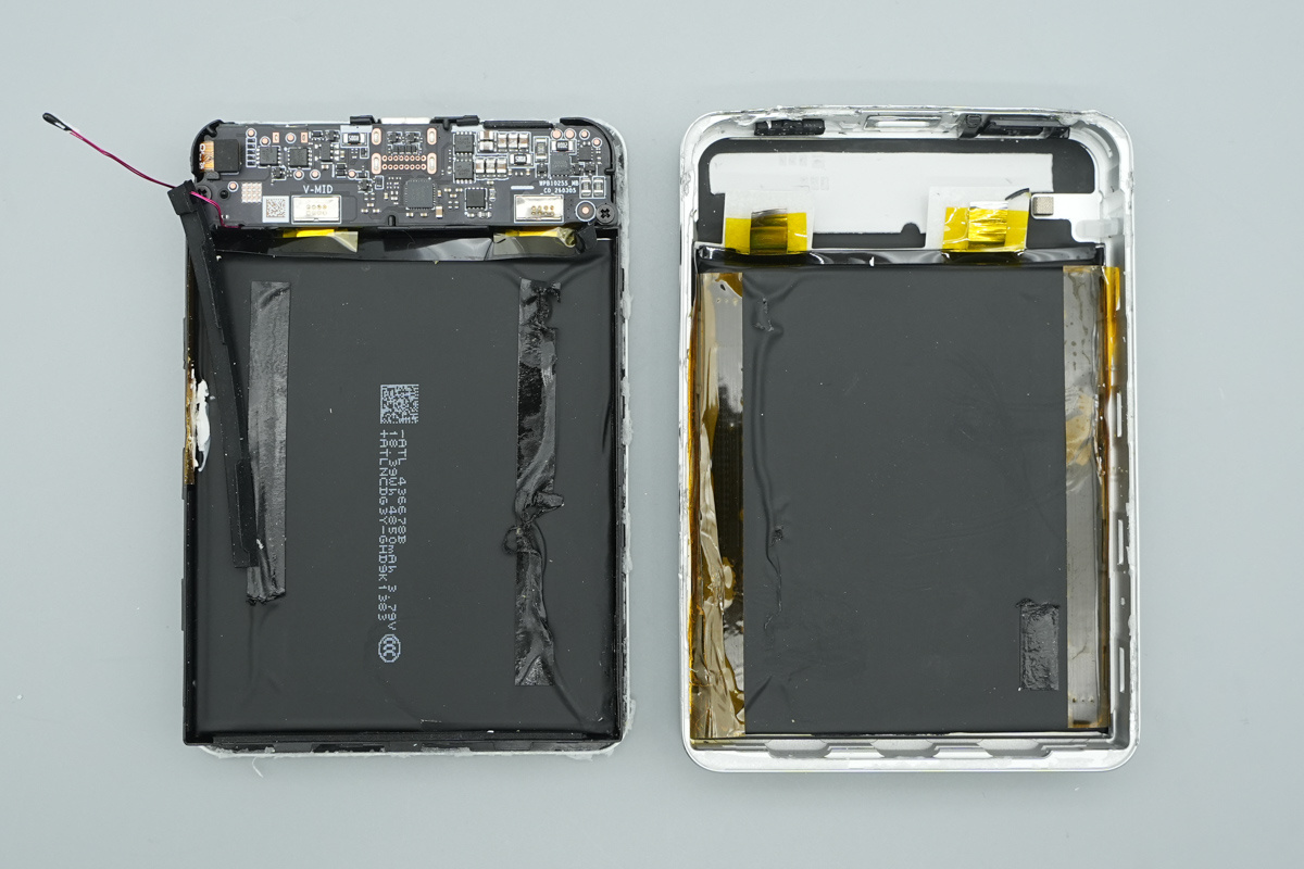
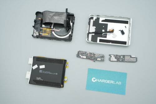
Proceeding to the teardown, after prying off the back cover, we remove one of the battery cells to reveal the internal battery pack and the PCBA. The battery pack consists of two cells.
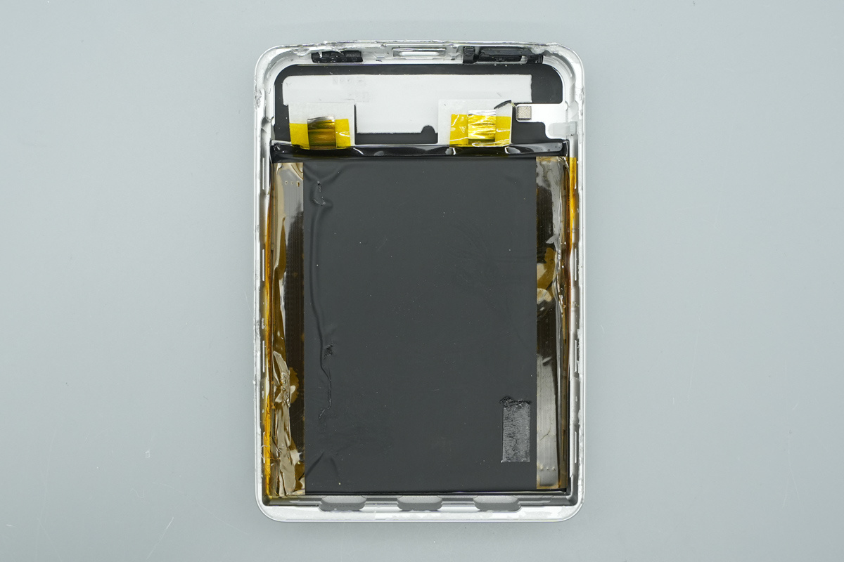
The interior of the removed casing reveals that one battery cell is attached to the aluminum shell, which is equipped with metal clips.
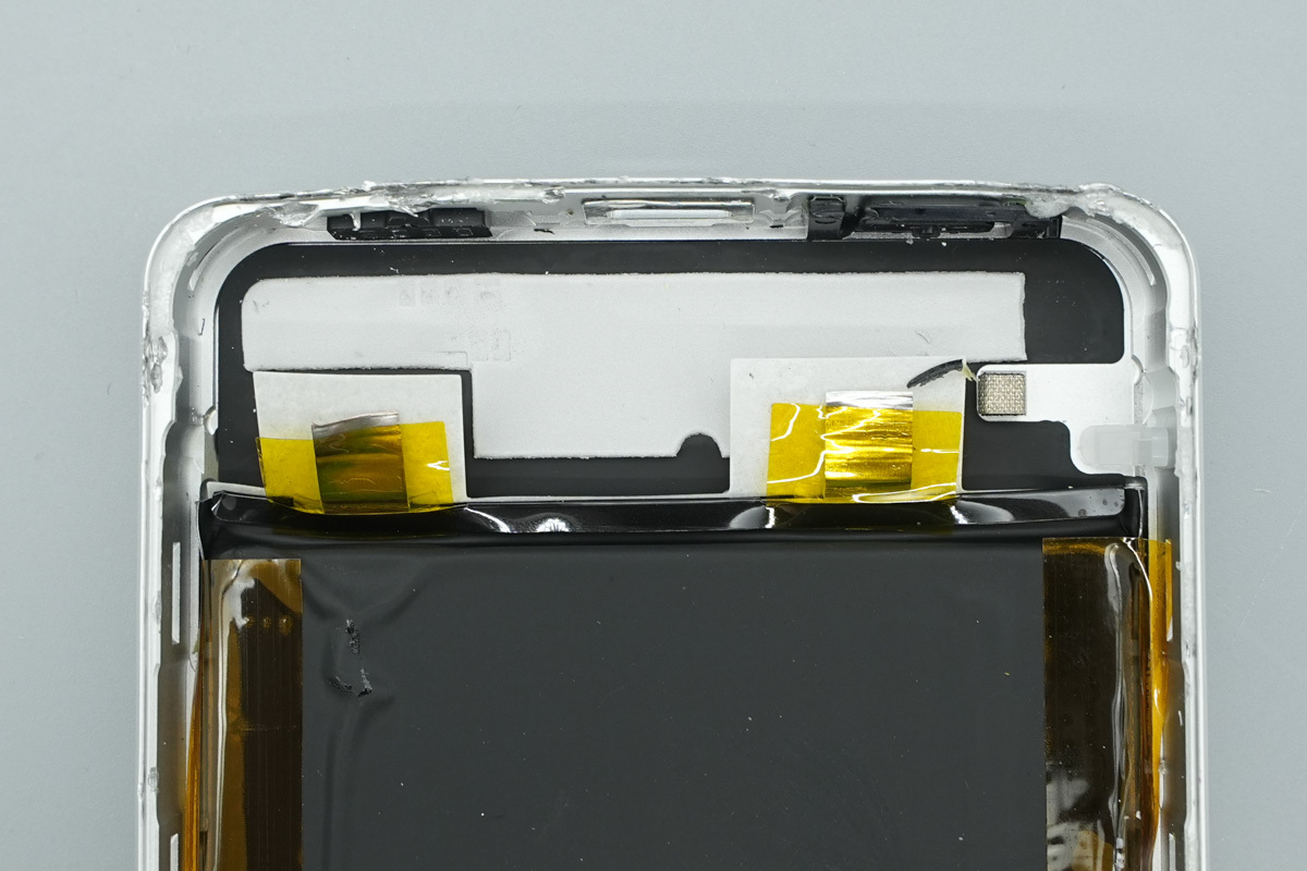
The battery tabs are fully insulated. The PCBA area is covered with cushioning foam and graphite thermal pads to provide protection and thermal management.
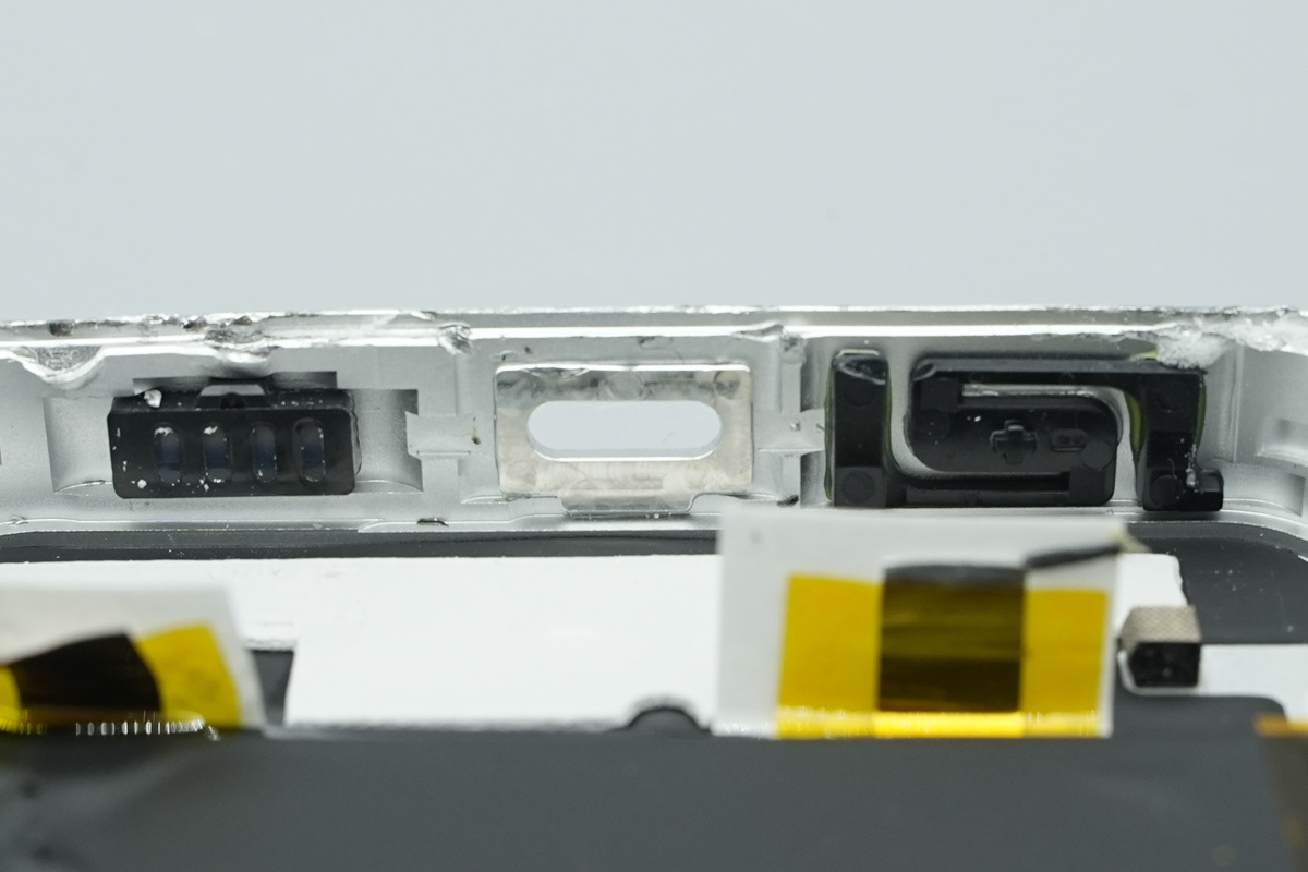
The USB-C port on the bottom is reinforced to ensure it stays stable and resists wear over time. Flanking the port, you'll find LED light guides and the power button.
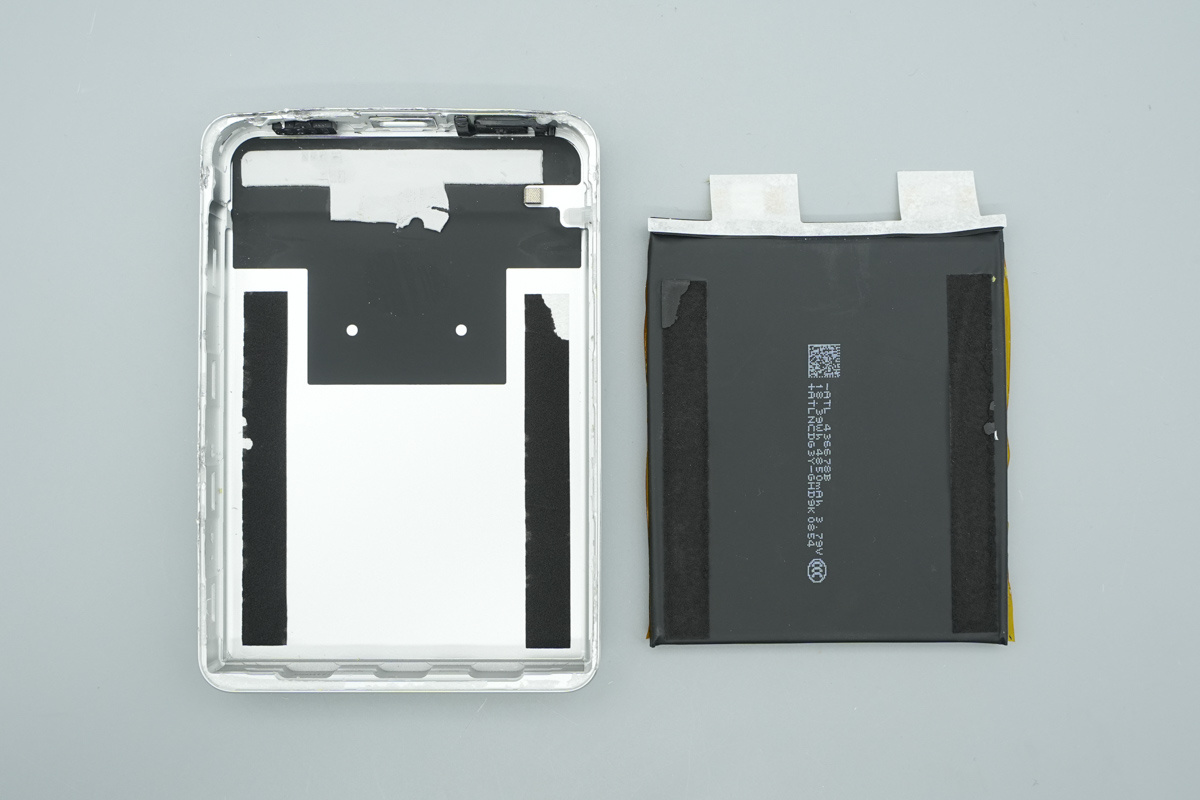
Separating the battery pack from the metal casing revealed that it was securely adhered with double-sided tape, alongside a clearly visible large graphite thermal pad.
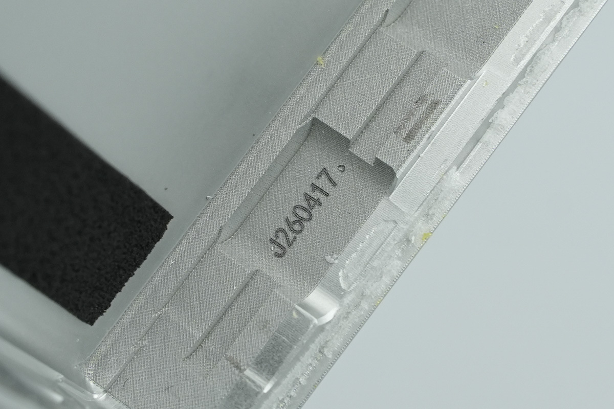
Inside the shell, we can clearly see the CNC machining marks and a laser-engraved production batch number (J260417).
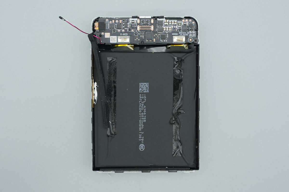
The other battery cell is connected to the PCBA, featuring an NTC thermistor probe on the left for real-time battery pack temperature monitoring.
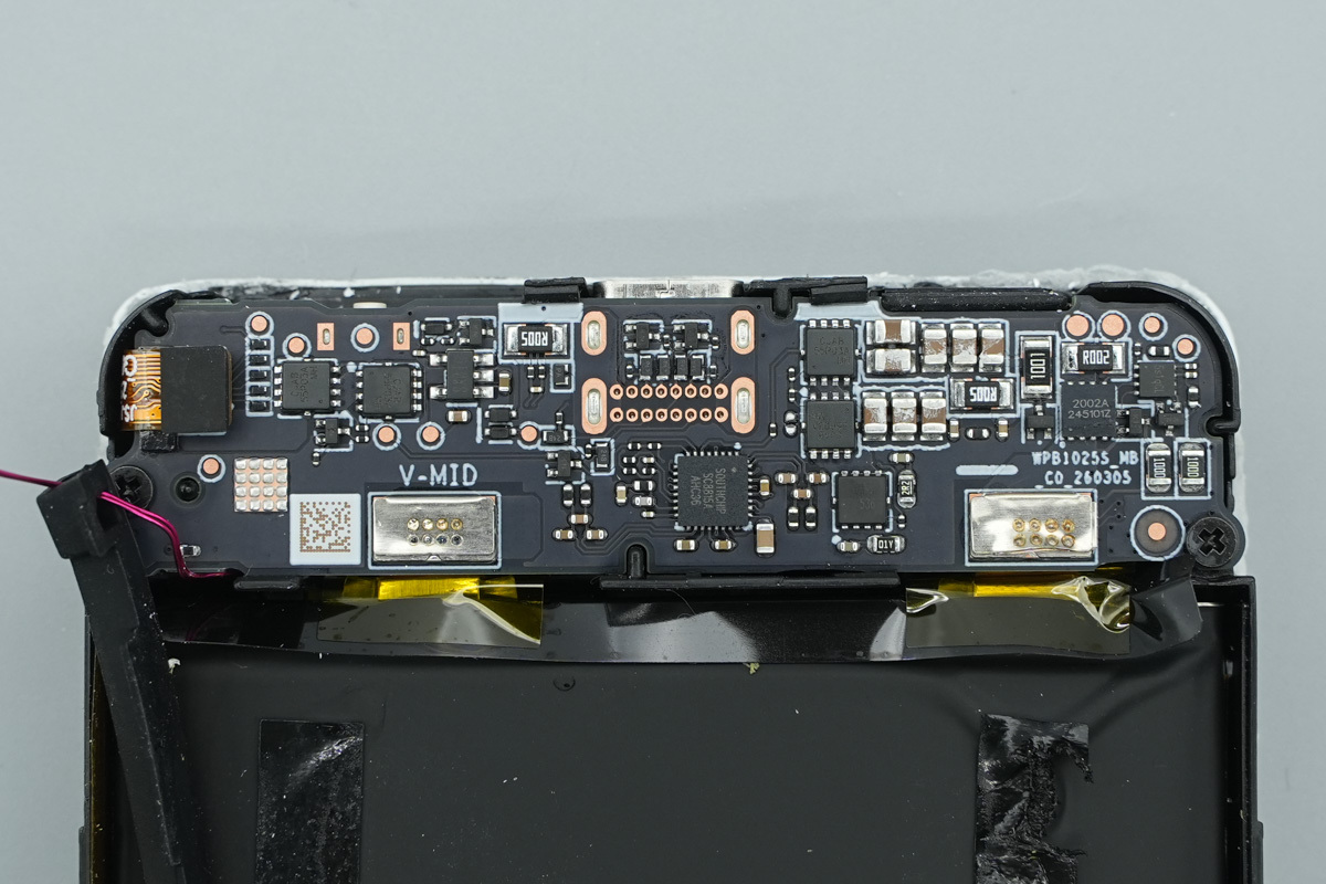
The PCBA consists of two modules, top and bottom, linked by a flexible cable on the left.
The battery cells are connected via spot-welding for a more secure and reliable fit.
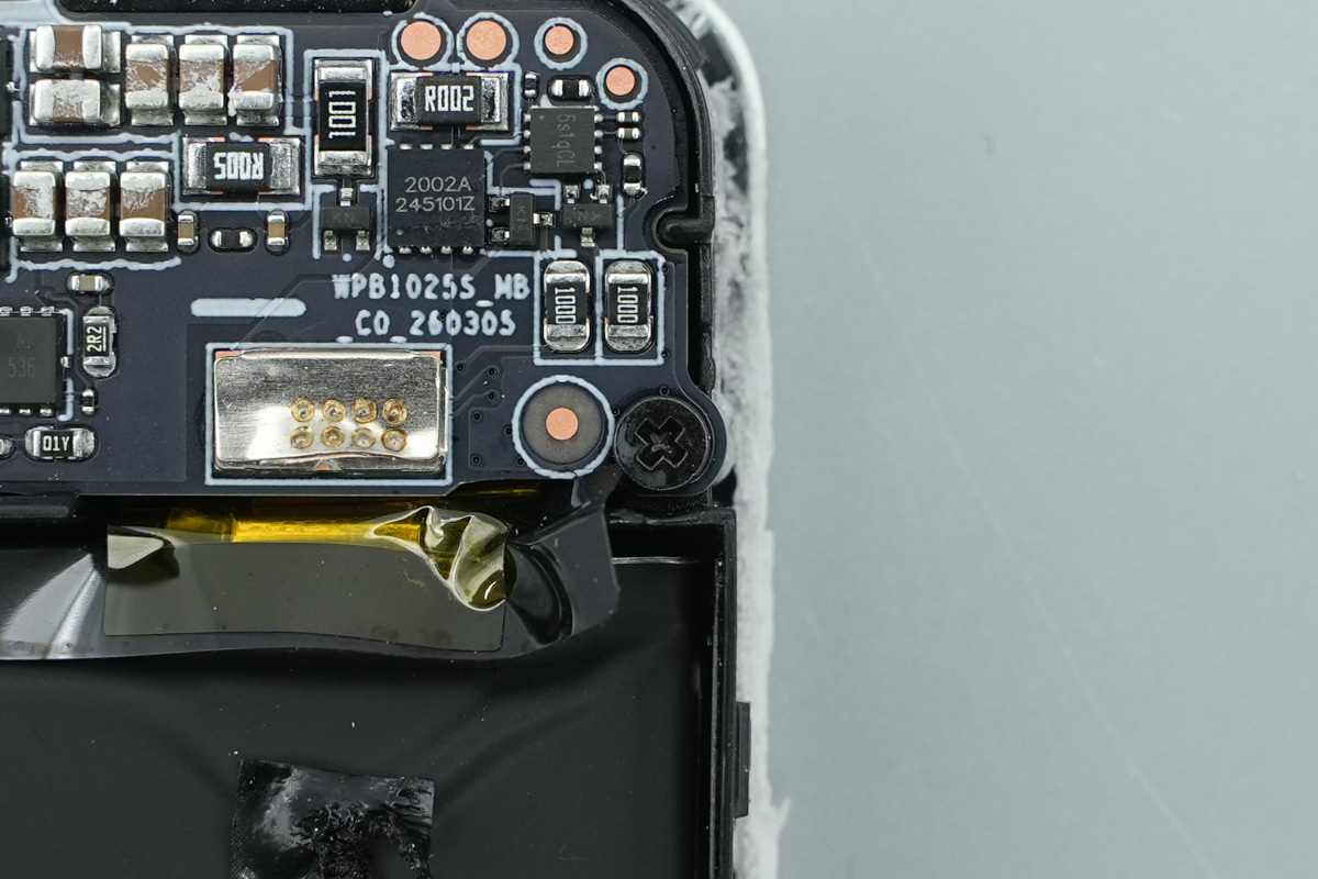
The PCBA module is fastened with screws.
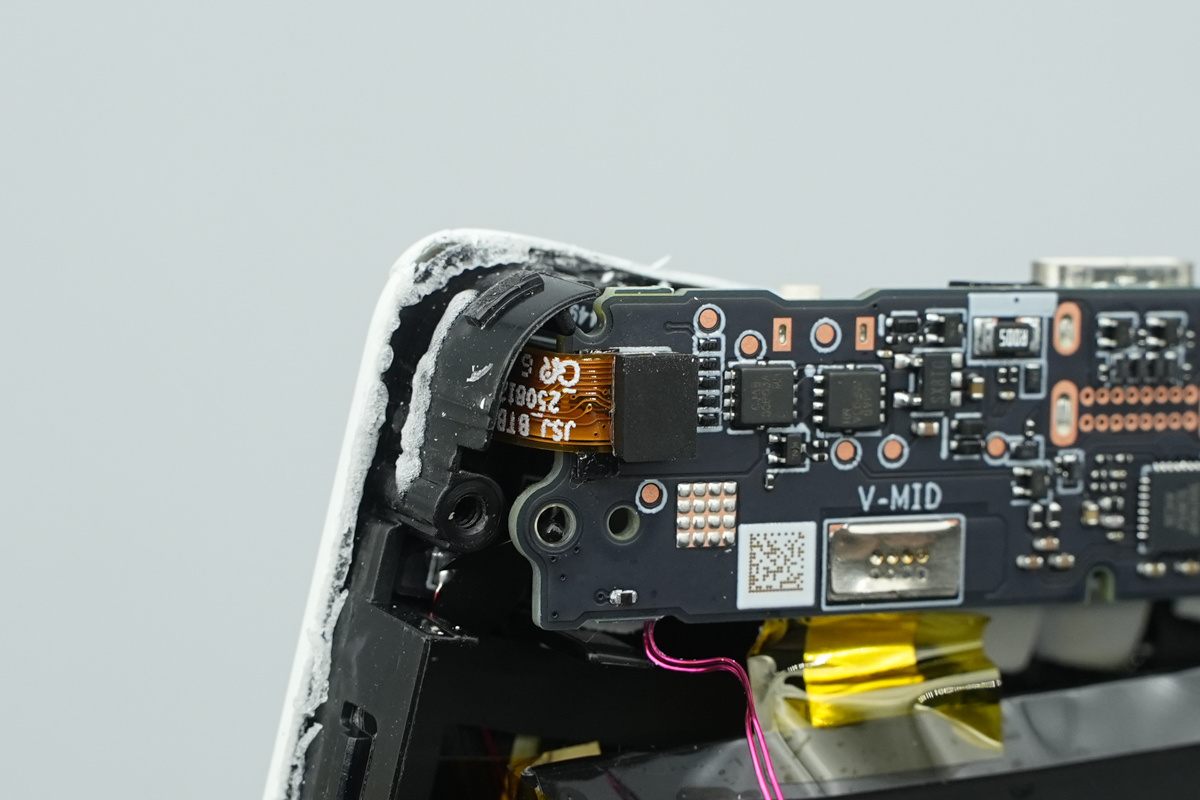
Removing the screws and lifting the top PCBA reveals the flexible cable connected on the left.
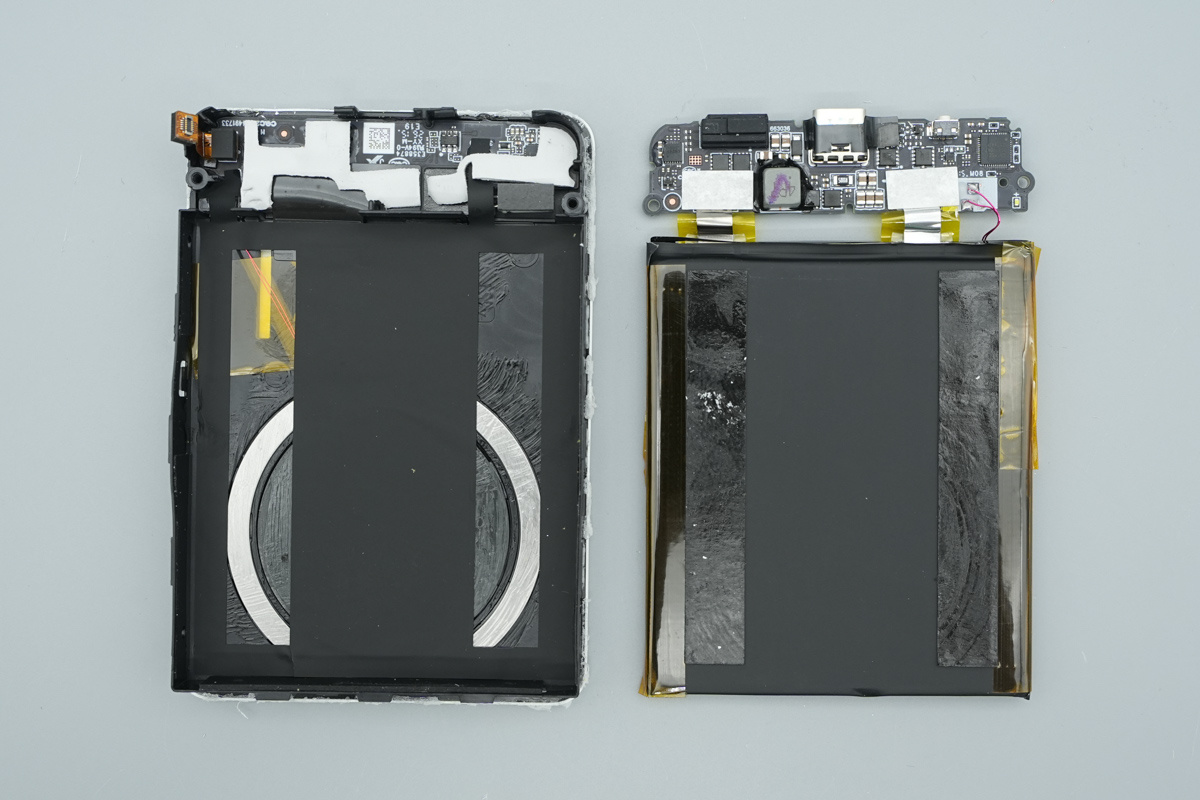
Removing the top PCBA reveals the magnetic wireless charging module underneath.
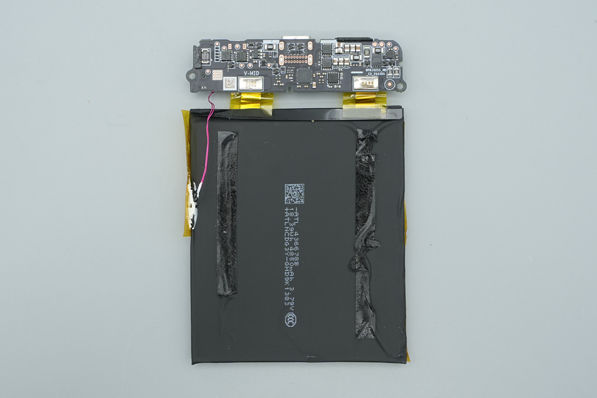
The top PCBA is connected to one of the battery cells situated below.
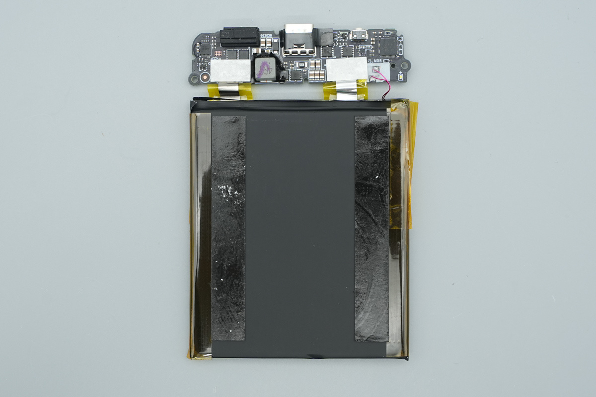
Insulation gaskets are also applied to the battery tab connections on the back.
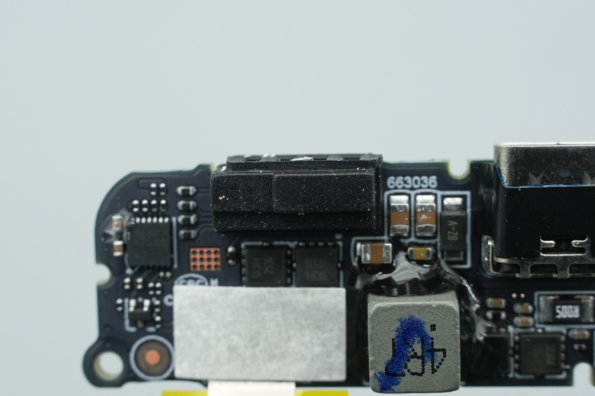
Foam light guides are used for the LED indicators to provide uniform brightness and reduce light leakage.
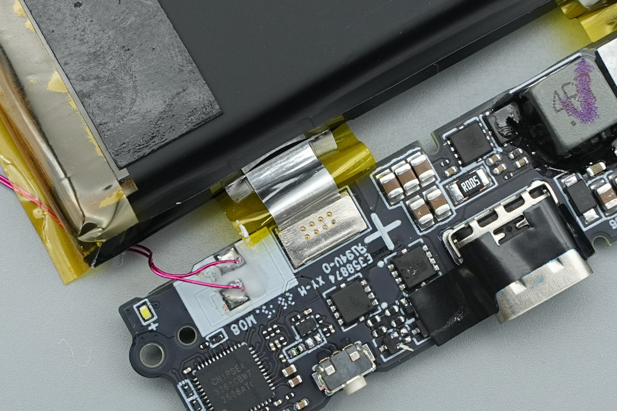
Removing the insulation gaskets, the positive and negative terminals are clearly seen connected to the PCBA by spot-welding.
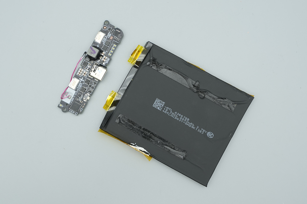
Separating the second battery cell from the main unit.
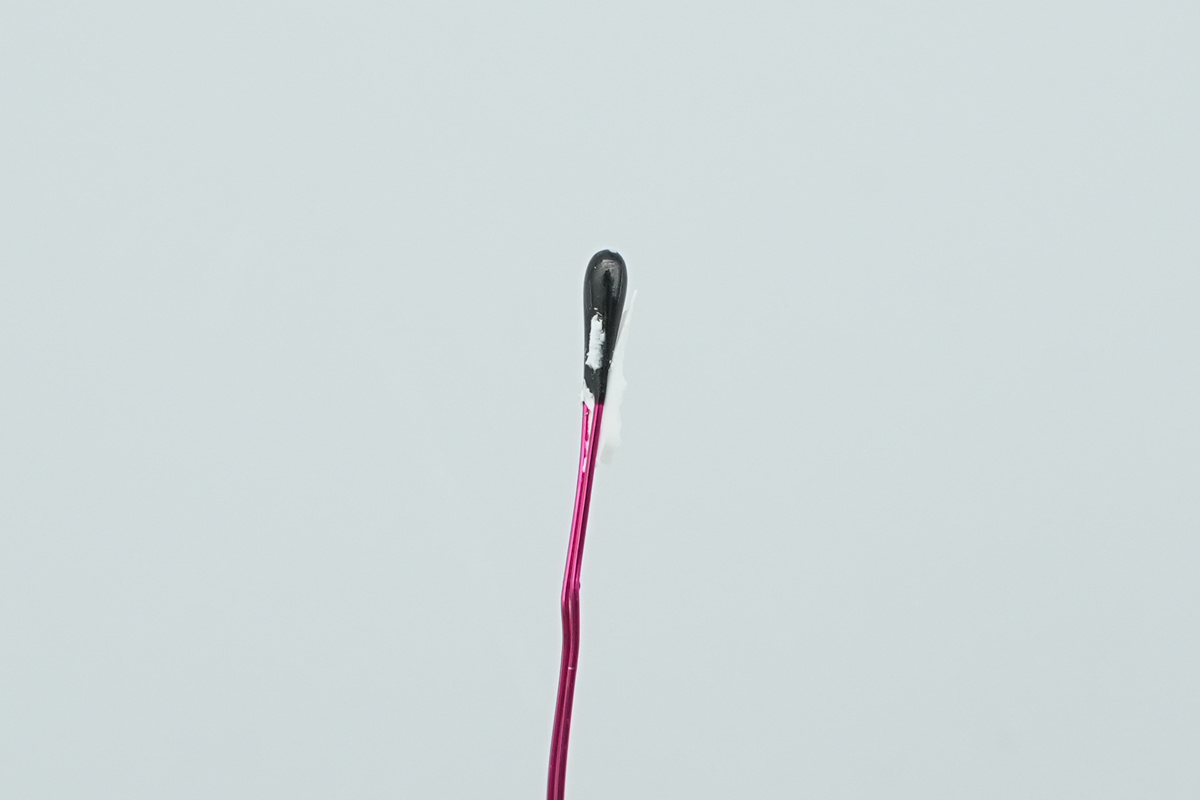
This is the NTC thermistor for battery temperature sensing.
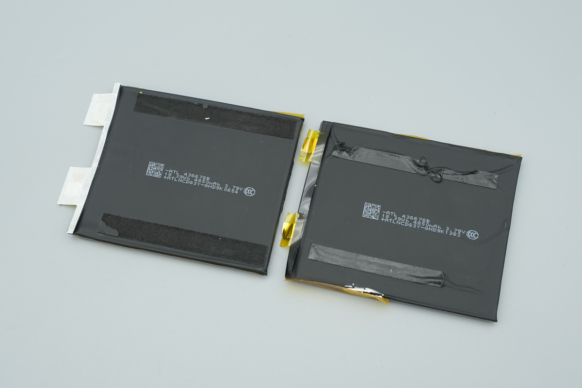
With that, we have now fully separated both internal battery cells.
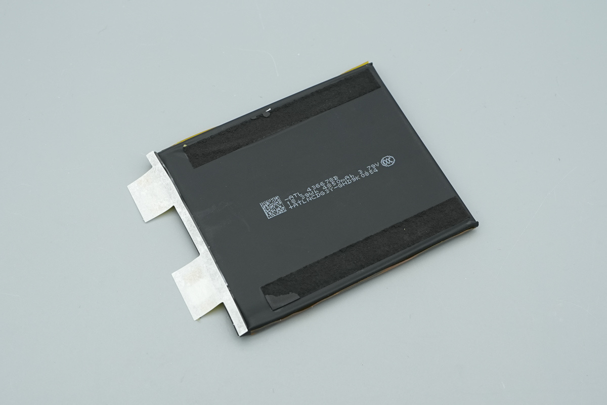
Moving on to the internal battery cells.
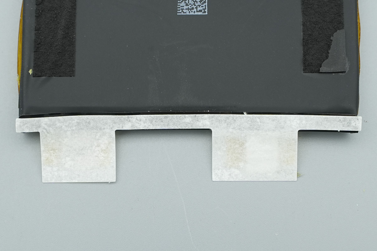
Insulation gaskets are applied over the battery tabs to protect against short circuits.
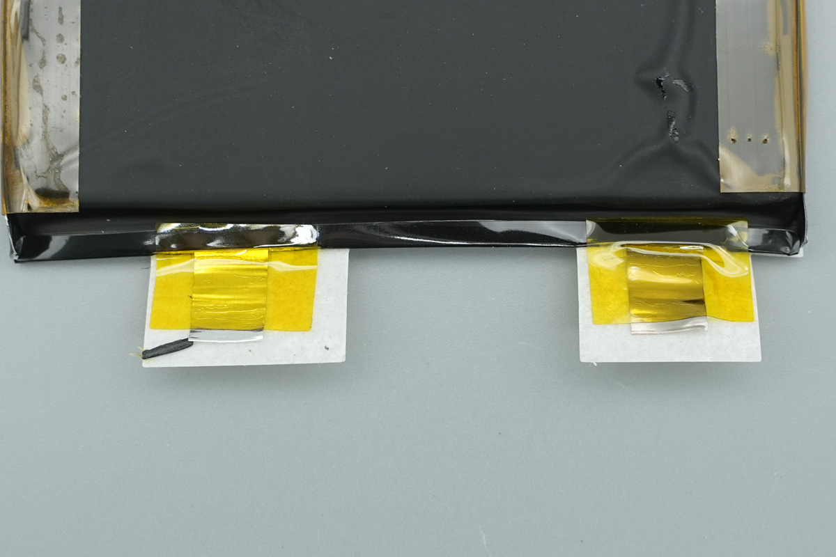
The other side of the tabs is covered with yellow high-temperature tape.
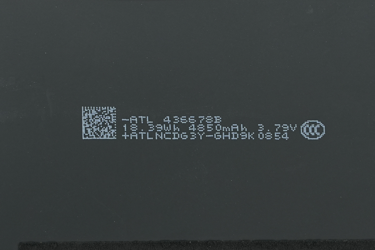
The battery cells are from ATL, featuring a 4850mAh (18.39Wh) capacity at a 3.79V nominal voltage.
The top PCBA integrates the protocol chip, the buck-boost MOSFETs, VBUS MOSFETs, LED indicators, the NTC thermistors, and the USB-C port.
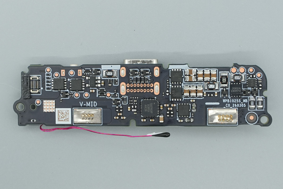
The back of the top PCBA features the buck-boost chip and the buck-boost MOSFETs.
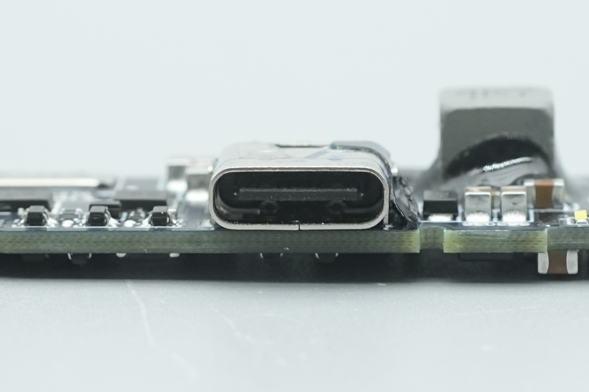
The USB-C port features a black plastic sheet.
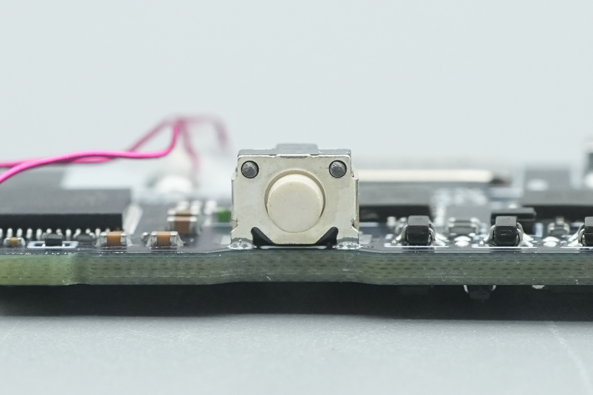
There is a single power button.
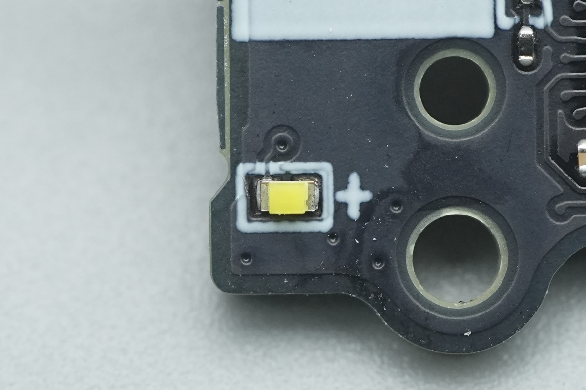
This is a SMD LED when charging.
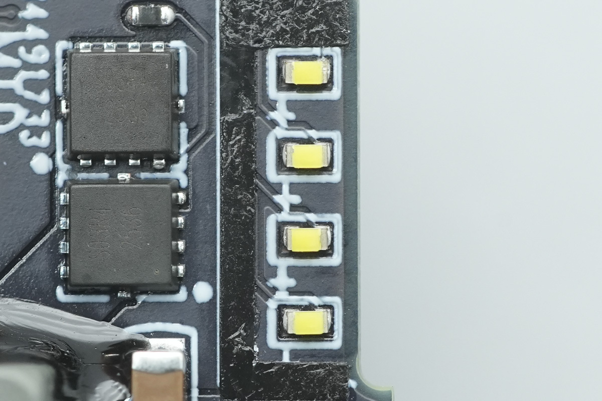
LED battery indicators are located on the other side.
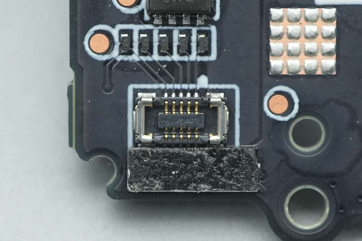
A BTB connector connects the bottom PCB.
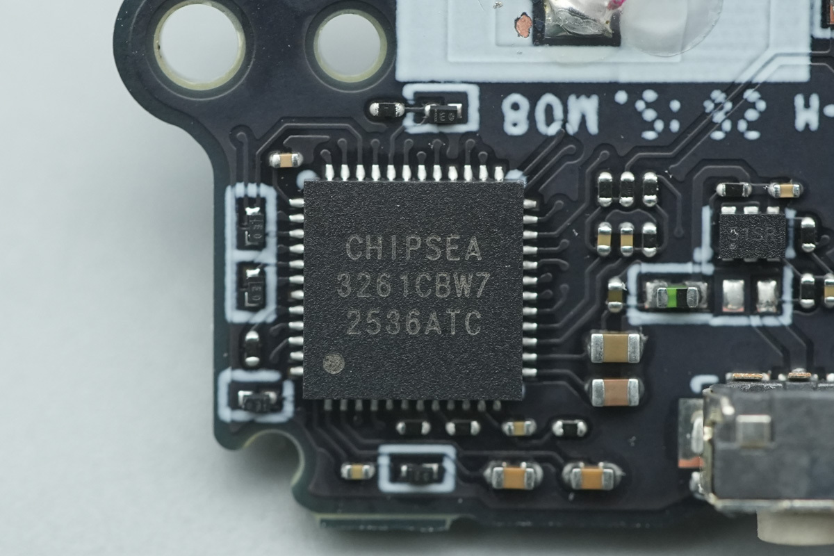
The CPW3261 from Chipsea is a versatile USB Type-C and PD controller, perfectly suited for power banks, BMS, wireless charging, and monitors. It packs a full suite of Type-C CC and USB PD features, plus USB BC1.2 compliance. To ensure maximum compatibility with the latest mobile devices, it also integrates support for a variety of mainstream fast-charging protocols.
At its core lies a 32-bit MCU clocked at 48MHz, delivering the high-performance computing power needed for complex industrial control. With 128KB of Flash, 24KB of SRAM, and extensive peripheral support—including I/O, USART, I2C, ADC, and a watchdog—the CPW3261 series offers developers the flexibility to deploy it across a wide range of sophisticated use cases.
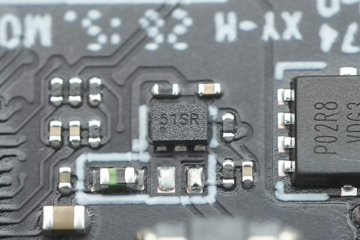
A chip, marked 51SR.
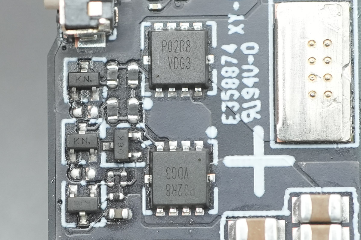
Two VBUS MOSFETs are from Prisemi, model PPM8PN02R8, PMOS, -20V and 5.6mΩ, housed in a PDFN3333-8L package.
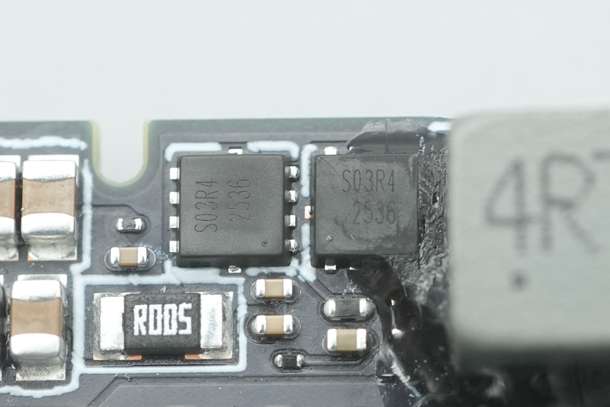
Two synchronous buck-boost MOSFETs are from Prisemi, model PSM8PN03R4, NMOS, 30V and 4.3mΩ, housed in a PDFN3333-8L package.
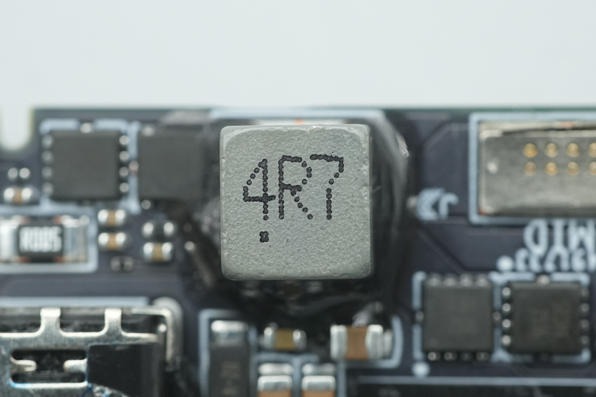
A synchronous buck-boost choke.
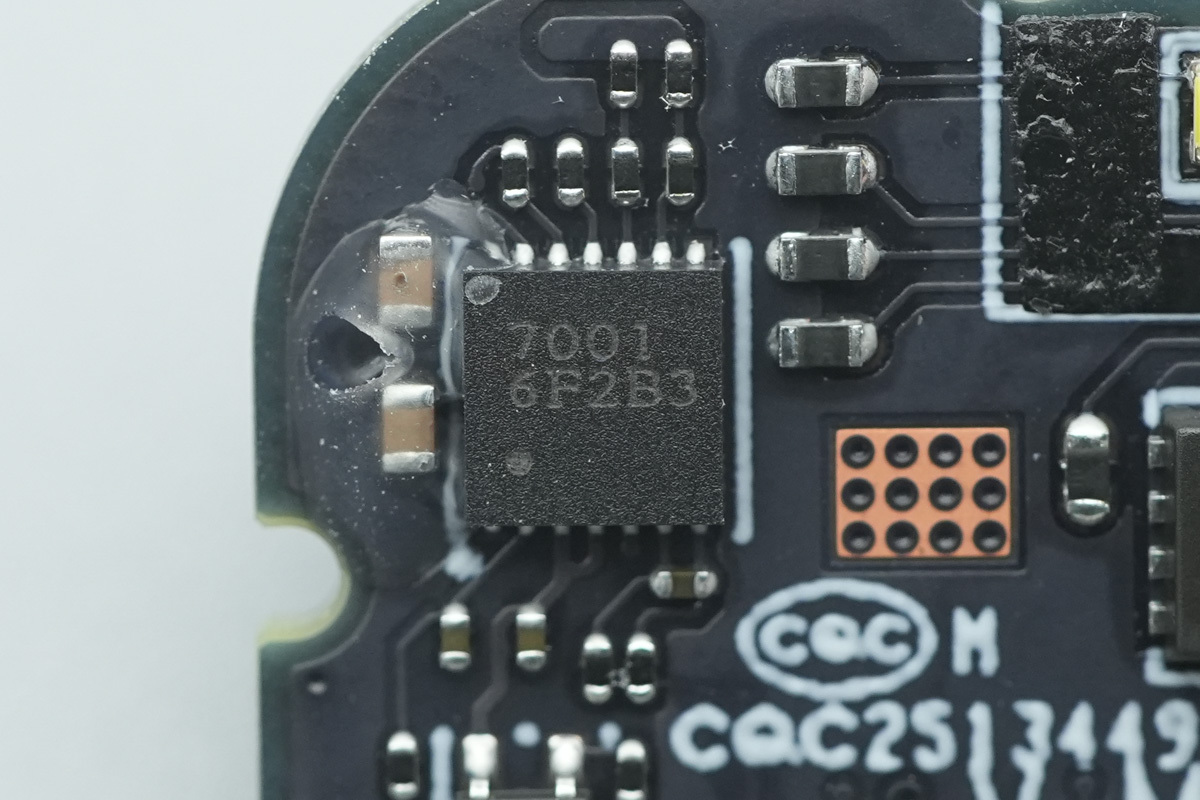
There is a device, marked 7001.
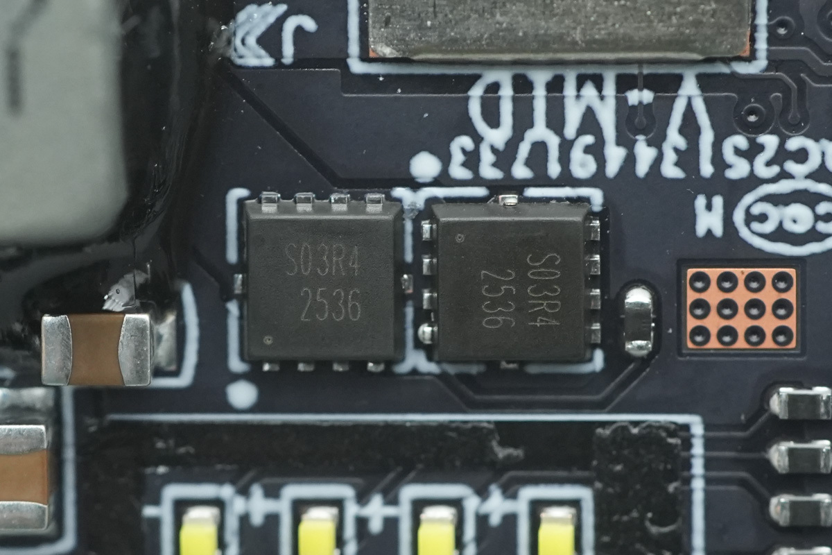
The synchronous buck-boost MOSFETs are from Prisemi, model PSM8PN03R4, NMOS, 30V and 4.3mΩ, housed in a PDFN3333-8L package.
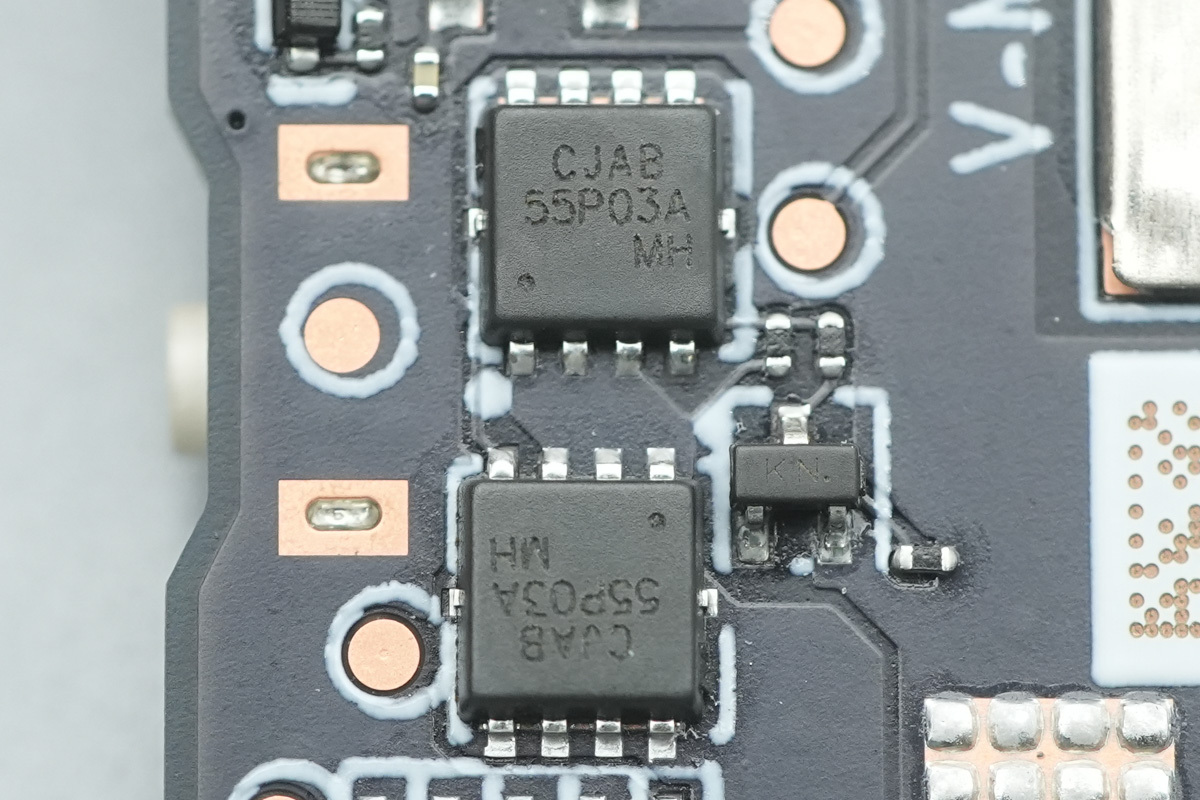
The power control MOSFET is from JSCJ, model CJAB55P03A, PMOS, -30V and 6.5mΩ, housed in a PDFNWB3333-8L package.
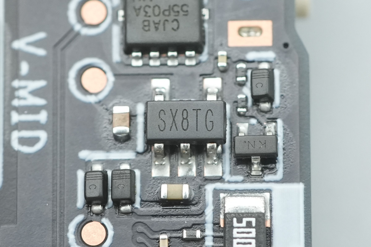
The LDO is from SGMICRO, model SGM2202, housed in an SOT23-5 package.
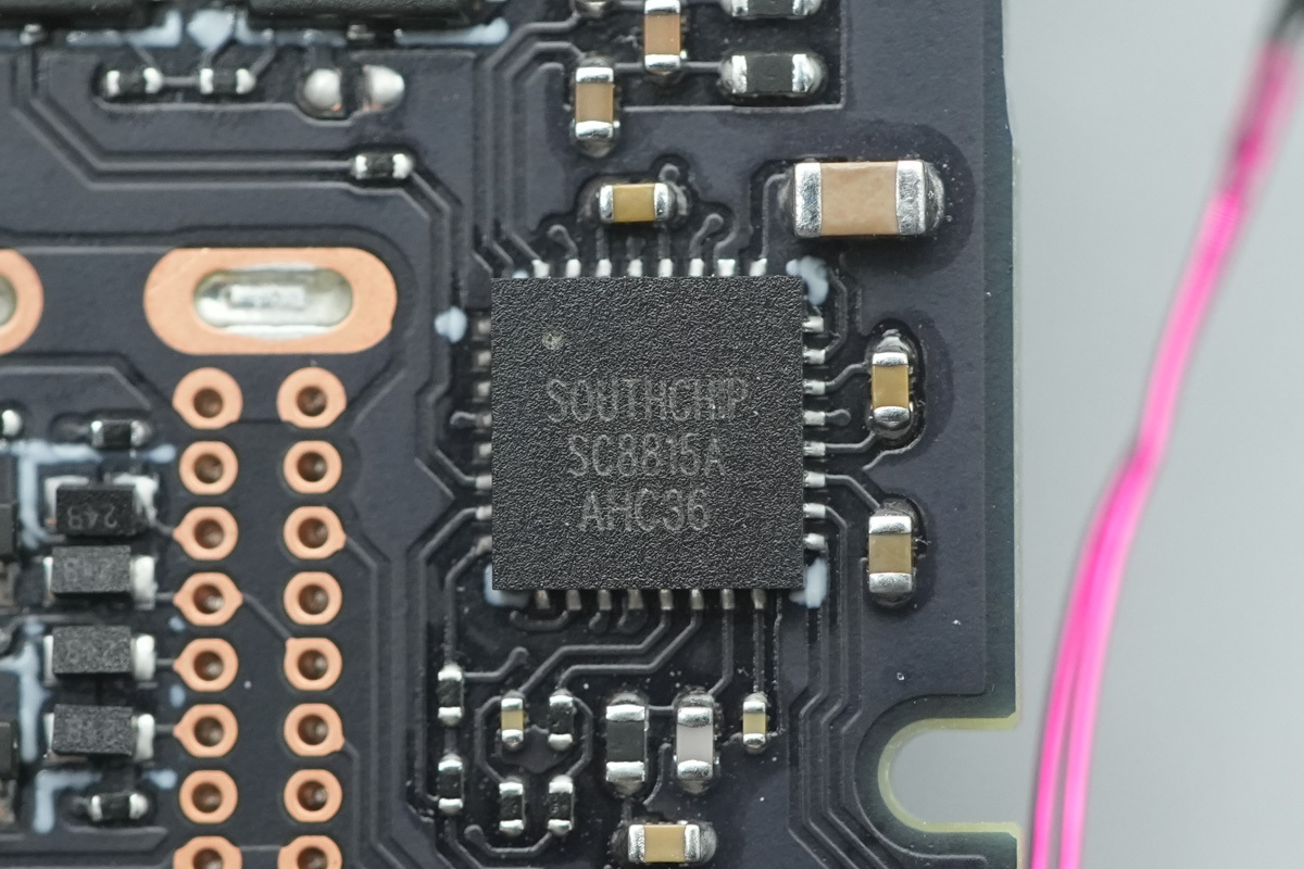
The synchronous buck-boost chip is from Southchip, model SC8815A. It is a high-efficiency bidirectional synchronous buck-boost controller that supports charging for 1 to 6-cell battery packs and features an I2C interface.
It provides comprehensive lithium-ion battery management, allowing for I2C-based programmable control over charging current, charging voltage, reverse discharge output voltage, and input/output current limits.
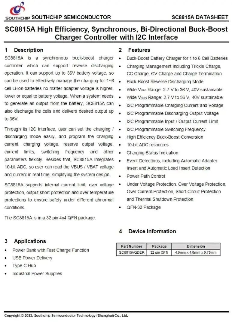
Featuring an internal 10-bit ADC, the SC8815A supports charging status feedback alongside automatic adapter and load detection. It also provides robust safety features, including UVP, OVP, OCP, SCP and OTP.
Designed in a QFN32 package, it is well-suited for PD-enabled power banks, USB-C hubs, and industrial power solutions.
Two additional VBUS MOSFETs are from JSCJ, model CJAB55P03A, PMOS, 30V and 6.5mΩ, housed in a PDFNWB3.3x3.3 package.
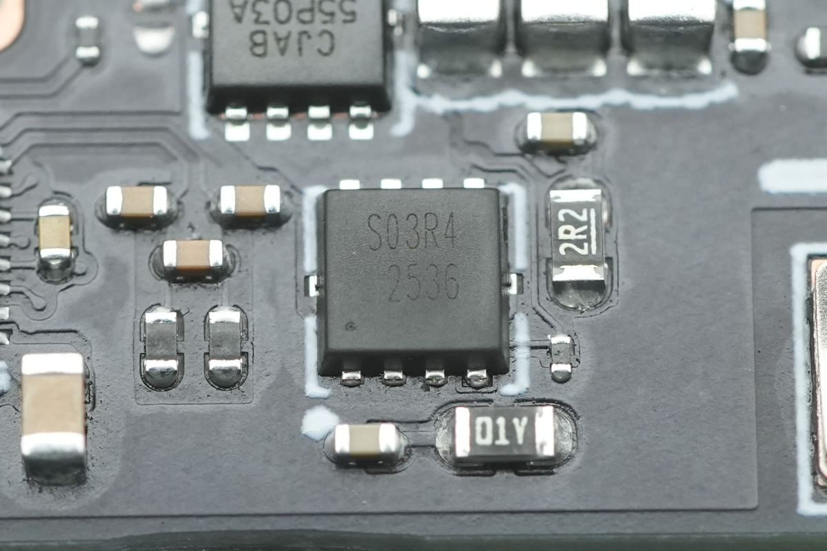
The power control MOSFET is also from Prisemi, model PSM8PN03R4.
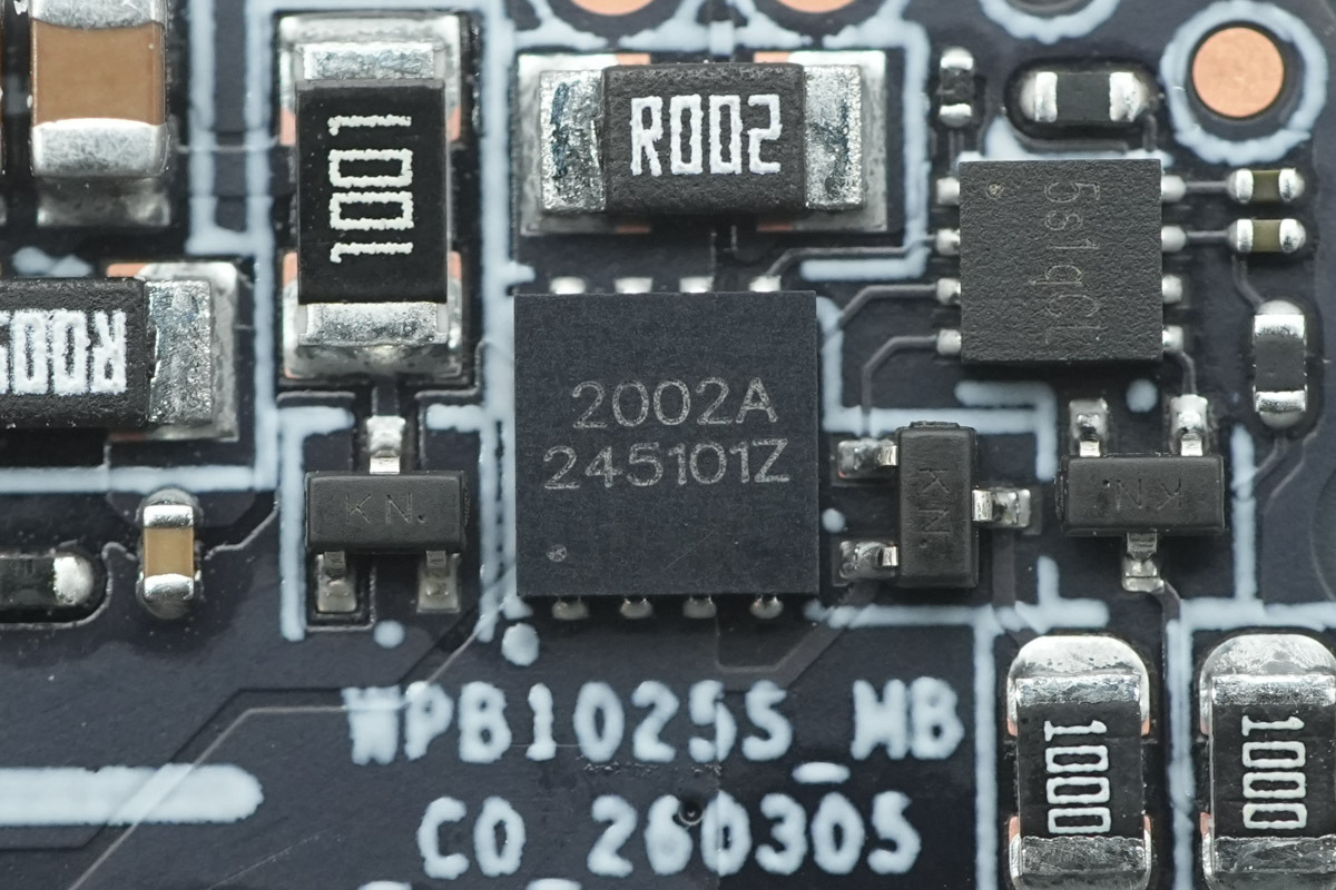
The battery protection MOSFET, marked 2002, is for battery overcharge, over-discharge, and overcurrent protection.
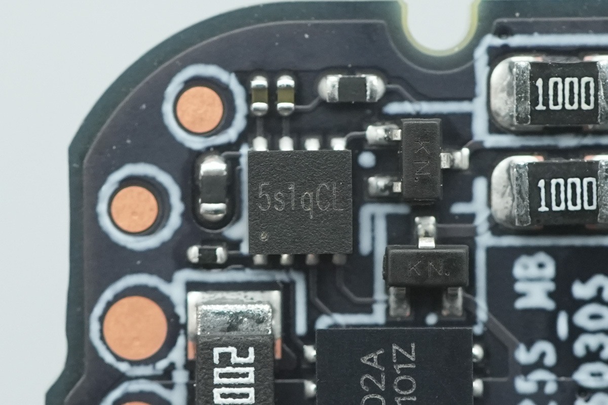
The battery protection IC, marked 5s1aCL.
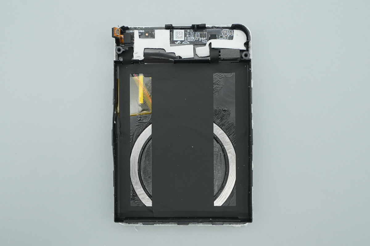
Moving on, let’s take a closer look at the internal bottom PCB and the wireless charging module.
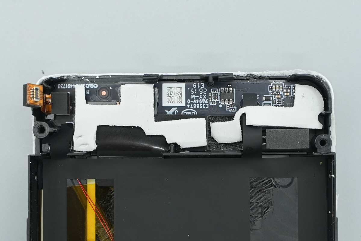
The bottom PCB features a large shock-absorbing foam cover to reduce drop-related damage.
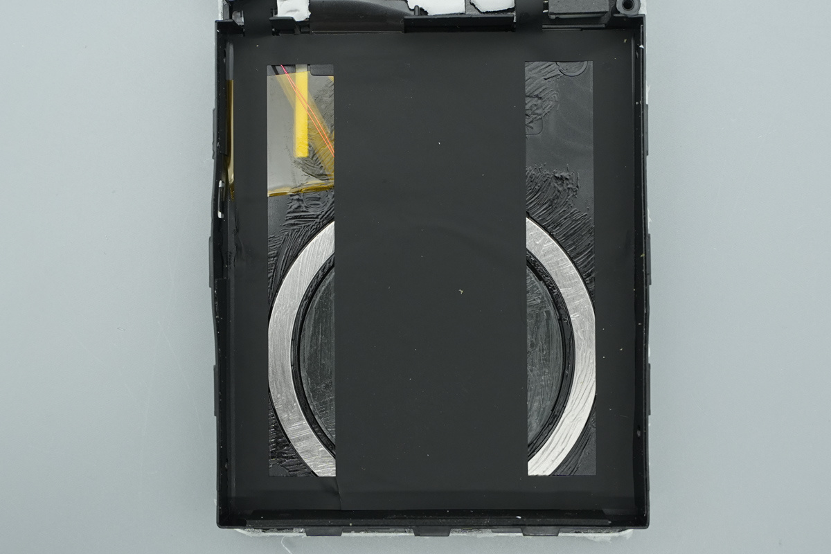
A large graphite thermal pad covers the magnetic wireless charging module.
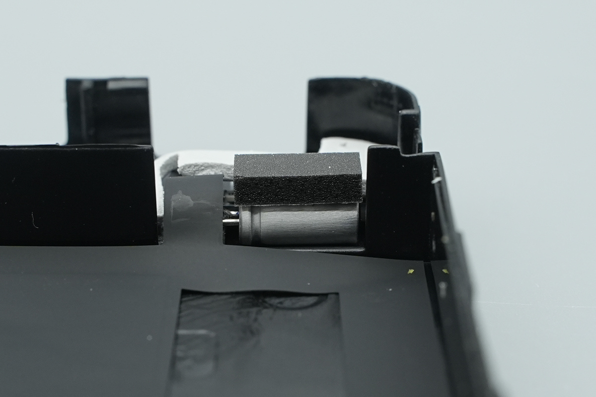
A foam pad is placed over the solid cap for cushioning and structural fixation.
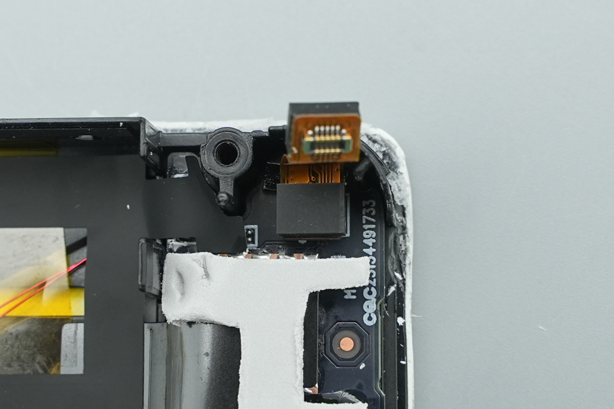
A FPC is located on the left side of the PCB, providing the interconnection to the upper PCB.
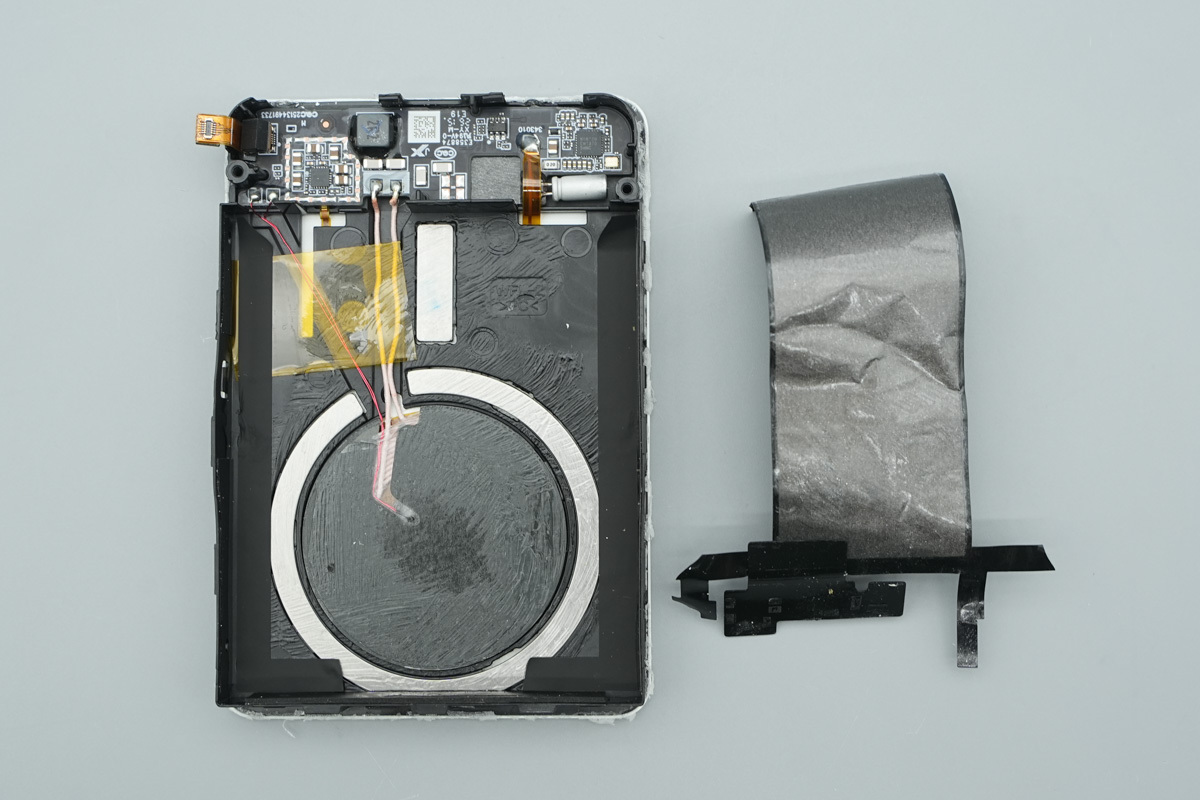
With the graphite thermal pads, cushioning foam, and EMI shielding removed, the internal structure is clearly visible.
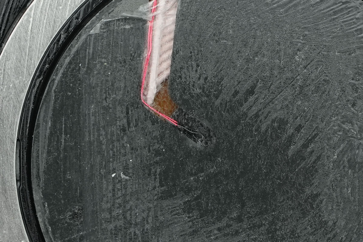
A dedicated NTC thermistor is positioned above the module for OTP.
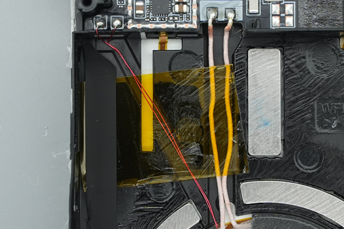
The wireless charging module cable is fixed in place with high-temperature tape.
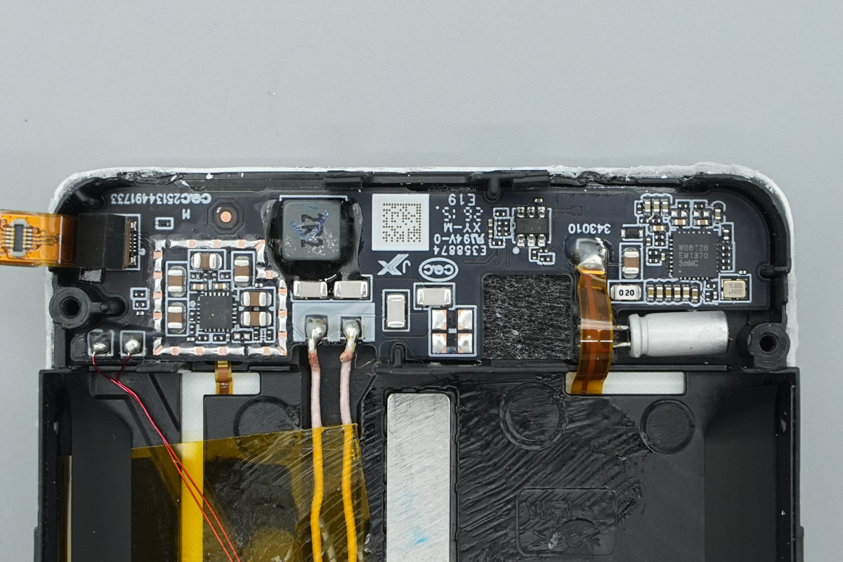
The NTC thermistor and Litz wire solder joints on the wireless charging module are clean and robust, and a touch-sensor cable is located on the right side.
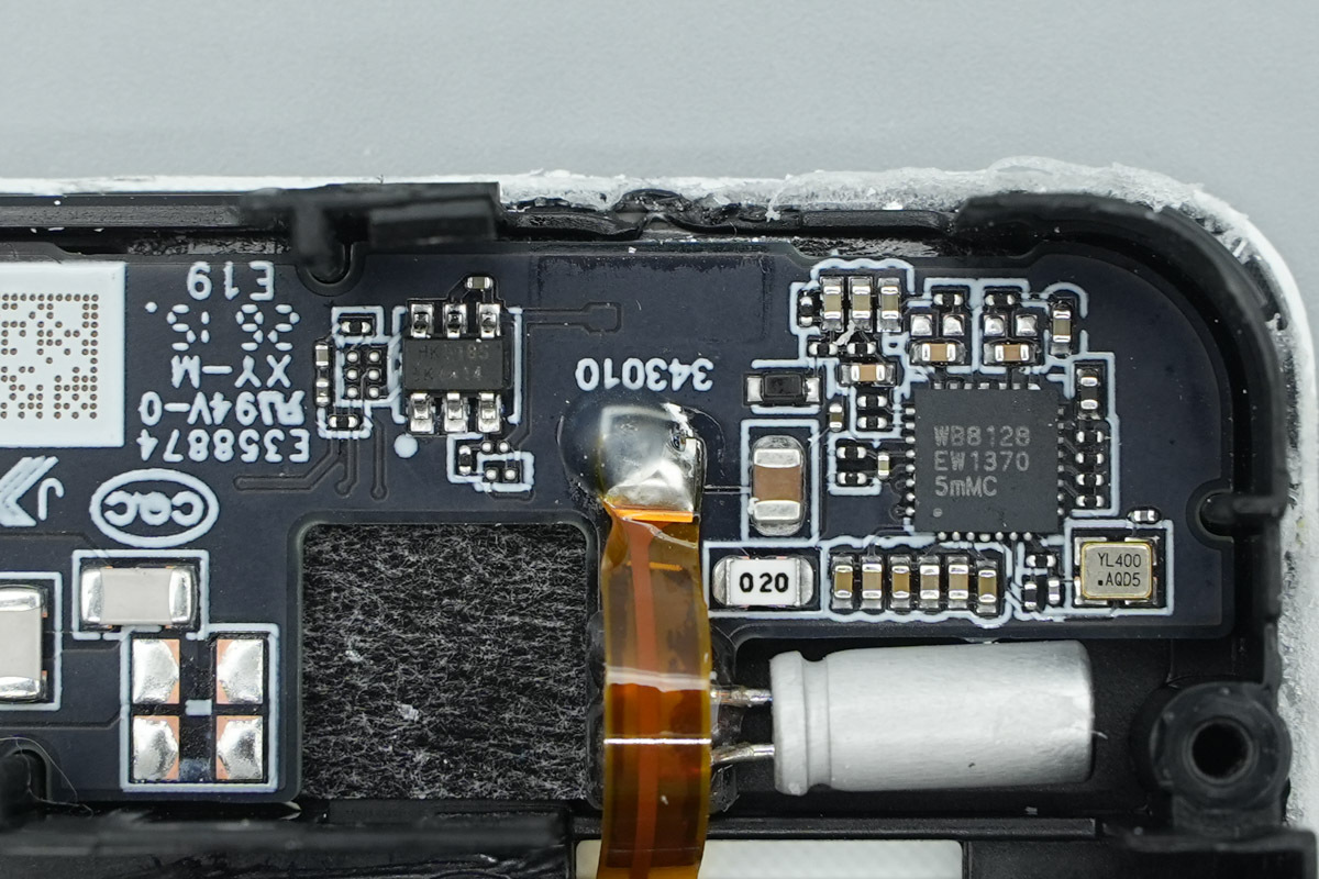
The touch-sensor cable features clean, well-formed solder joints and is secured with adhesive-fixed to ensure reliable detection of magnetic charging.
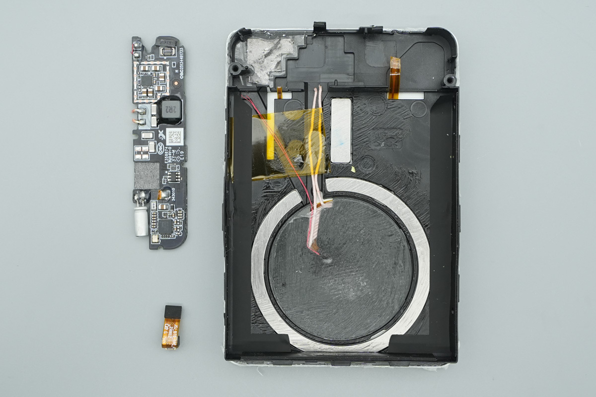
Separating the bottom PCB from the front panel.
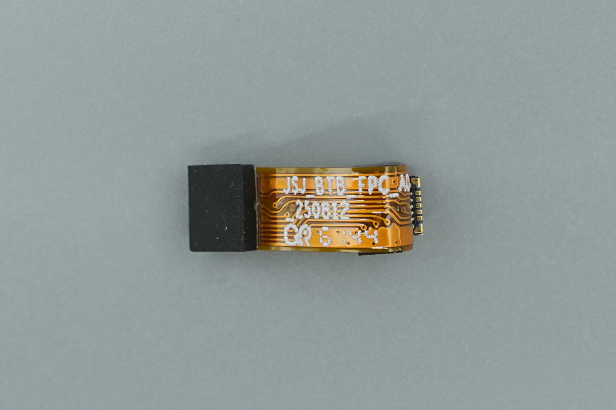
There is a FPC, marked JSJ_BTB_FPC.
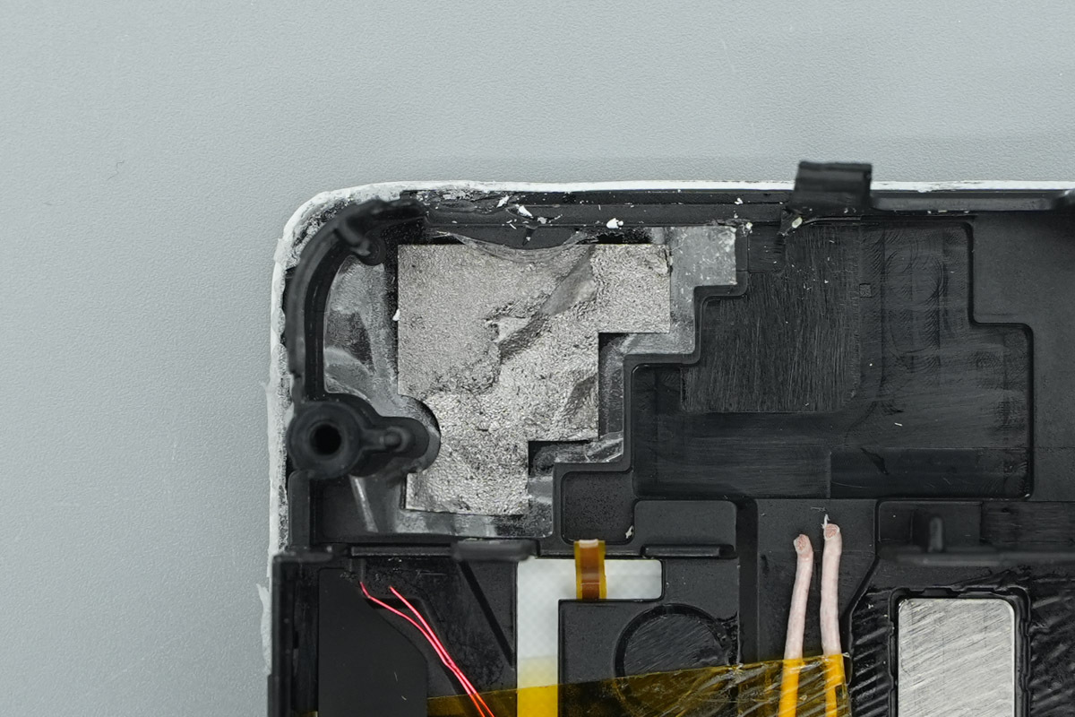
A graphite thermal pad is placed on the upper-left corner of the housing to accelerate heat dissipation.
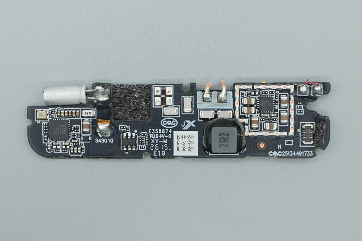
The front side of the bottom PCBA features low-voltage solid filtering caps, the wireless charging chip, and the buck-boost chip.
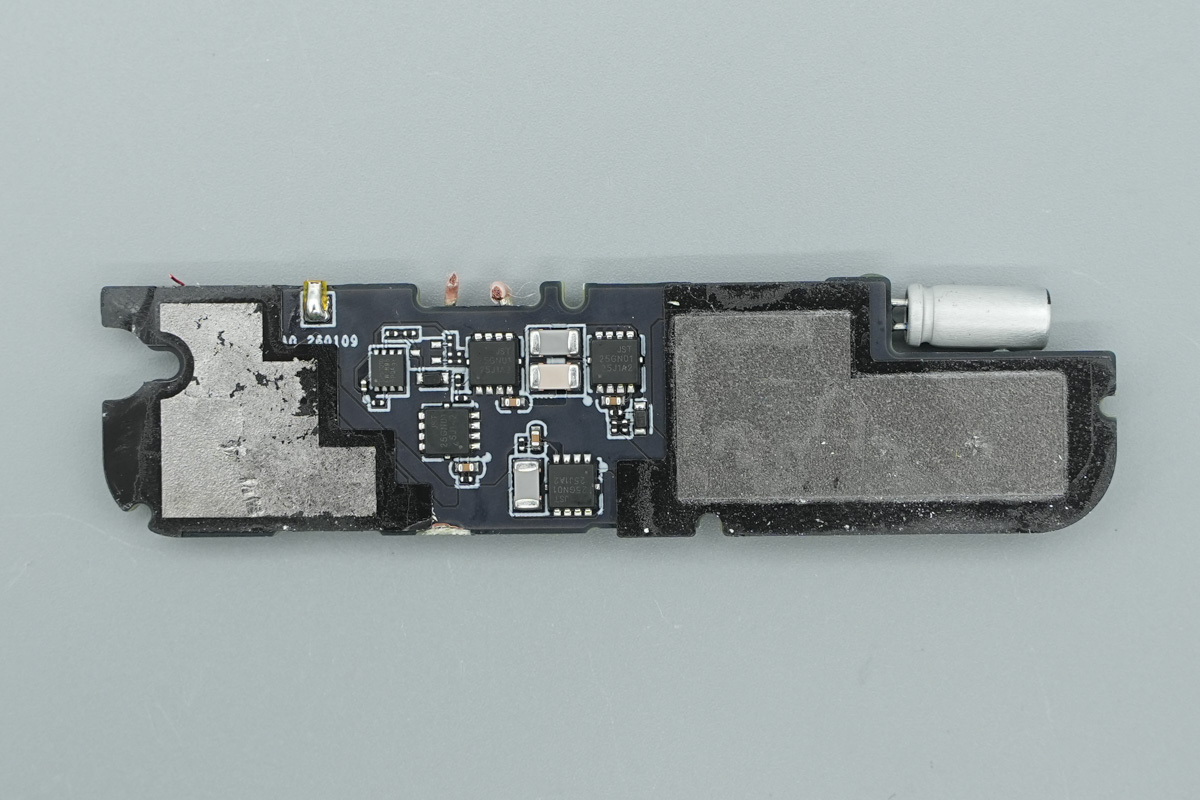
The rear side houses the wireless charging power MOSFETs and authentication chip, while large graphite thermal pads on both sides ensure efficient heat management.
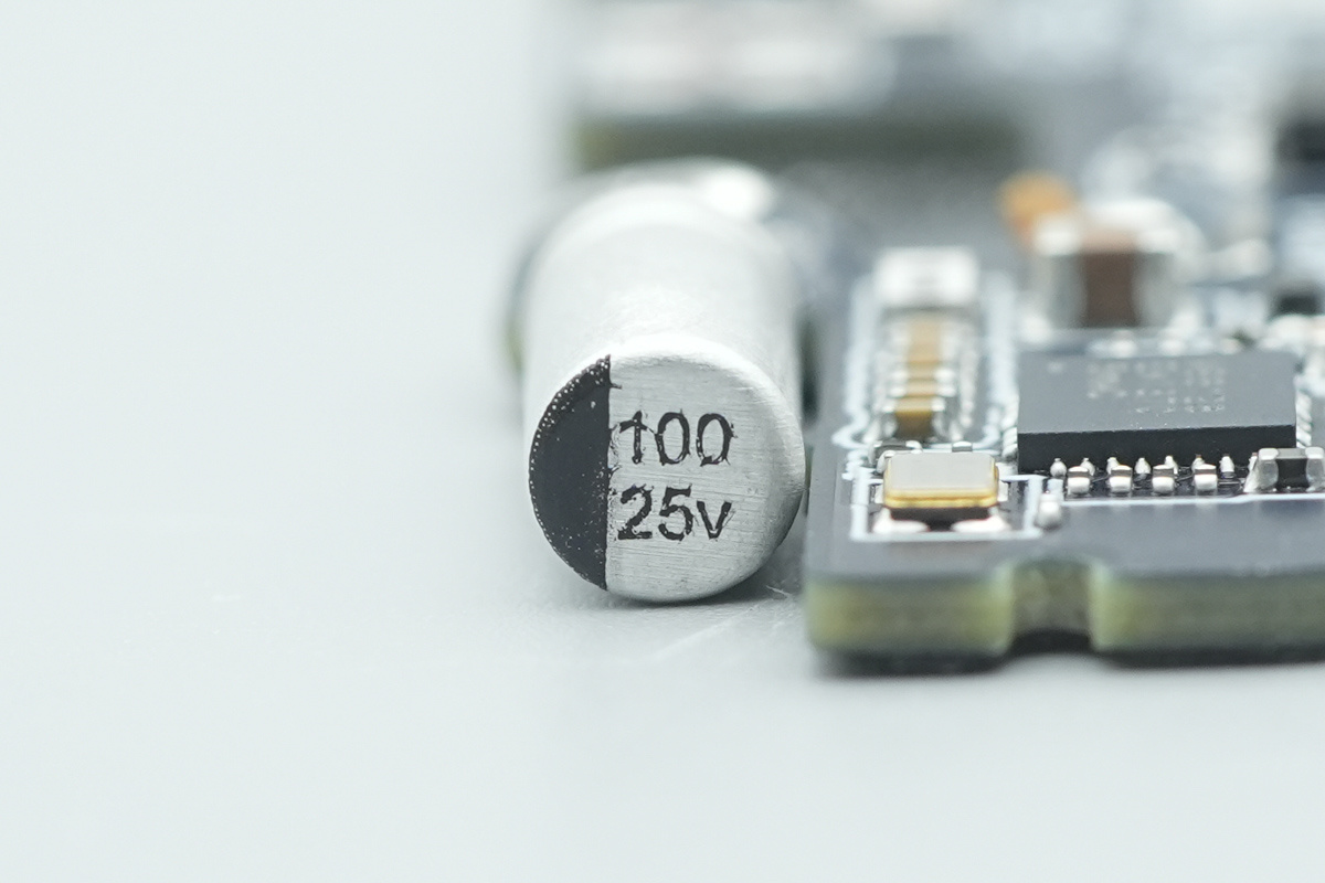
A low-voltage solid filtering cap, 25V 100μF.
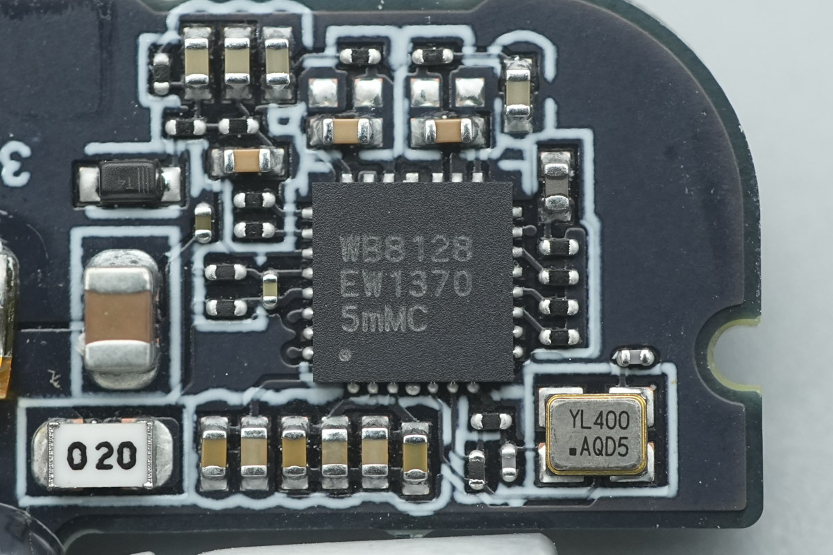
The wireless power transmitter chip is from CPS, model WB8128. It is a highly integrated 30W Qi wireless power transmitter controller that supports Qi2.2, MPP, and Samsung fast charging protocols, with an input voltage range of 3.3V to 24V.
Internally, it integrates a 32-bit MCU, 32KB of MTP, PWM drivers, and FSK PHY modulation/demodulation, enabling efficient control of the wireless transmitter coil for stable power output.
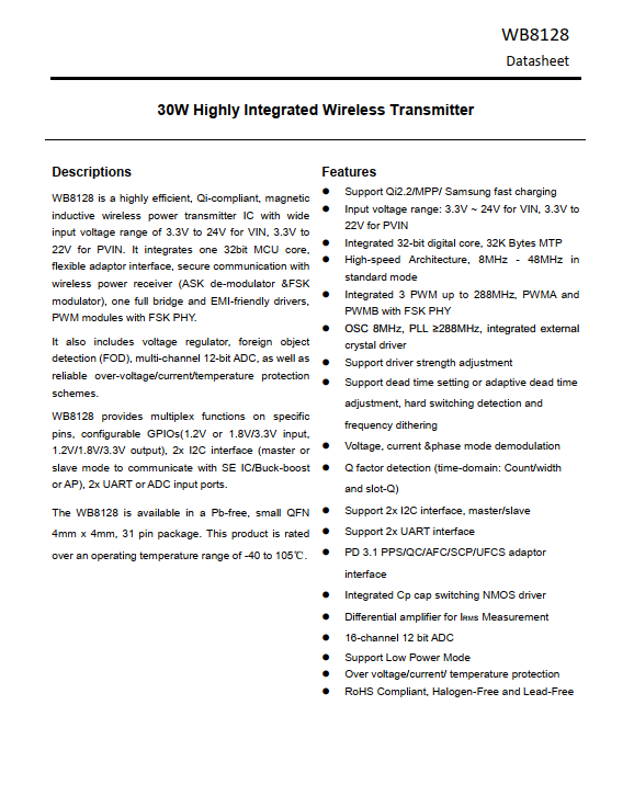
The chip provides 2× I²C master/slave interfaces, 2× UARTs, and multiple GPIOs. It features an integrated 16-channel 12-bit ADC for voltage, current, and temperature monitoring, alongside robust safety mechanisms include FOD, OVP, OCP, and OTP.
Housed in a QFN31 package, supports -40°C to 105°C operation, and meets RoHS and halogen-free requirements, offering a highly integrated, reliable solution for medium-to-high power wireless charging.
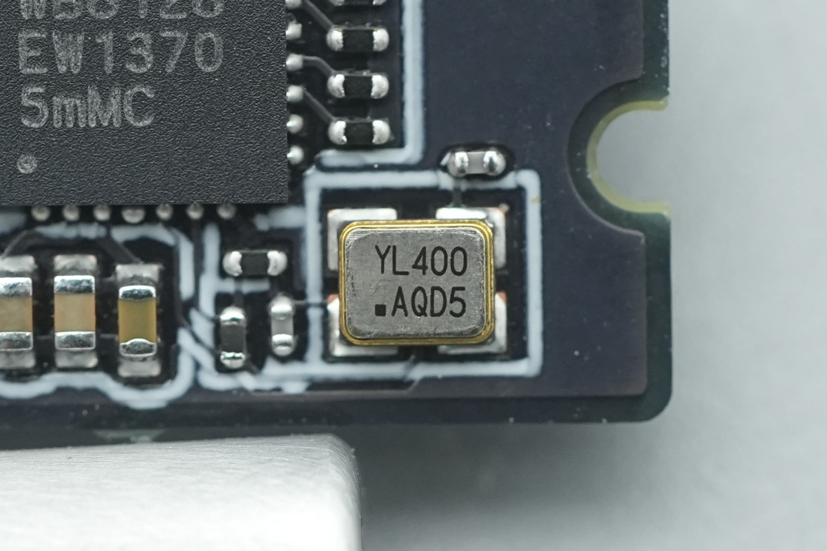
A crystal oscillator provides the clock signal for the wireless charging chip.
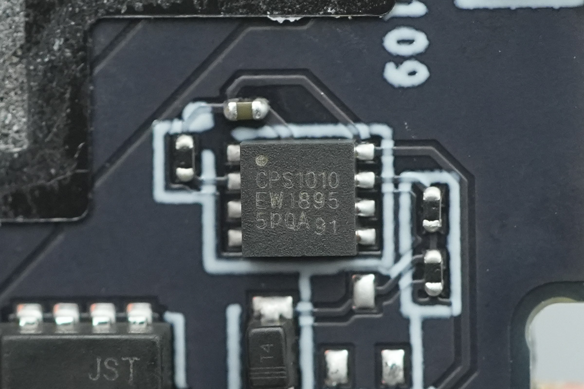
The authentication chip is from CPS, model CPS1010, a dedicated wireless charging protocol security IC designed for Qi-certified applications.
It integrates a SHA256 cryptographic engine, ECC signing, and a true random number generator to facilitate secure identity and protocol authentication. It is housed in a DFN8 package.
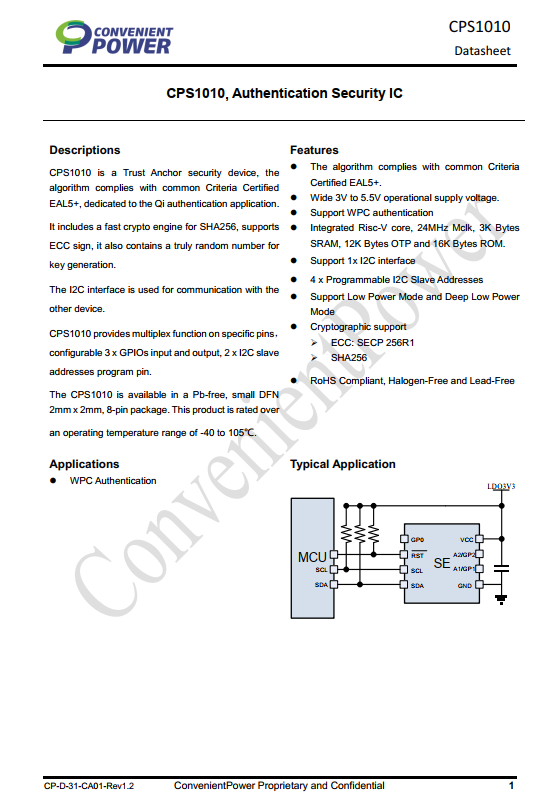
Here is the info about CPS CPS1010.
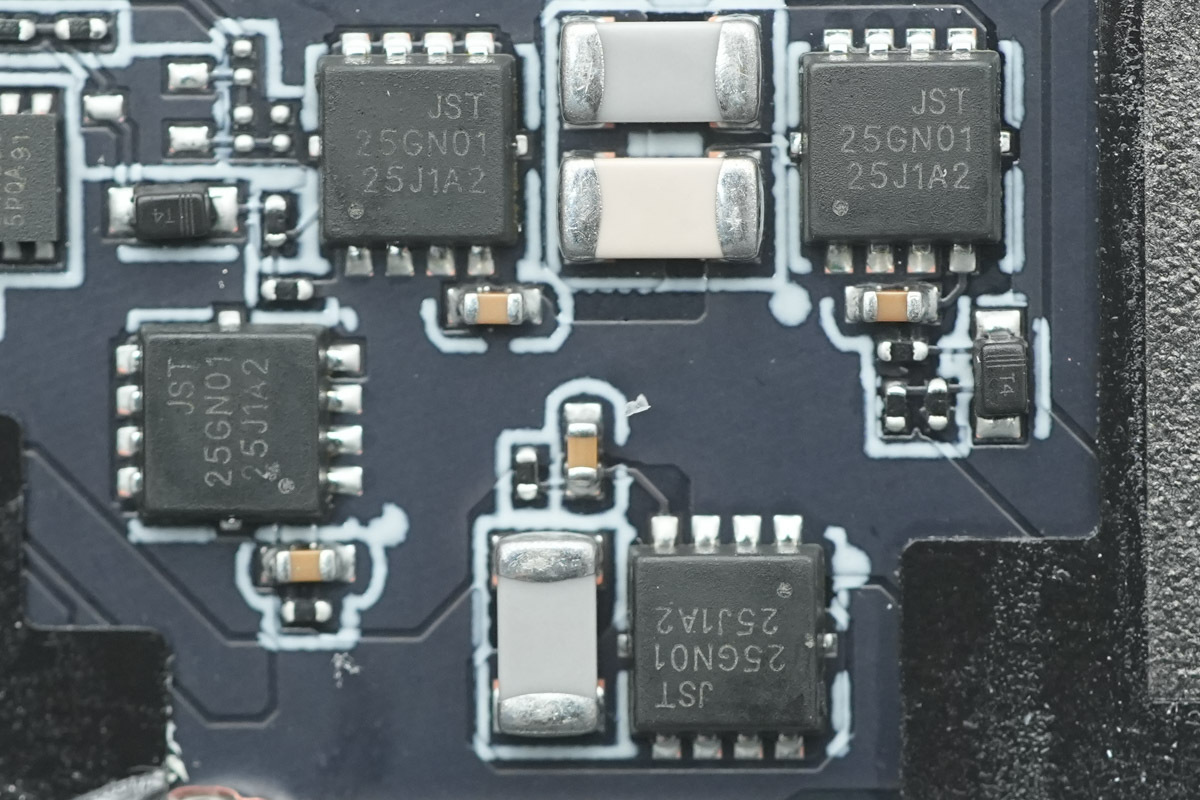
The wireless charging power MOSFETs are from JST, marked JST25GN01.
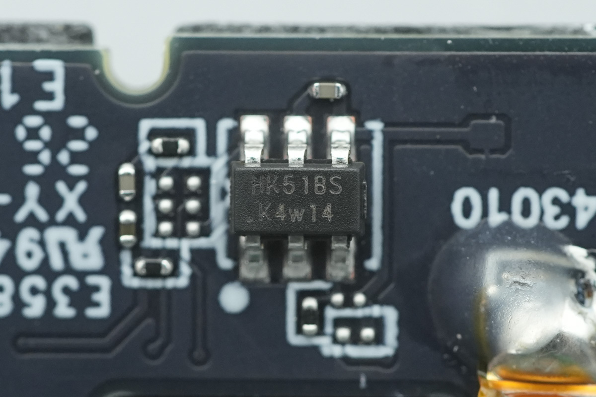
The touch sensor chip is from HYNITRON, model HK51BS, housed in an SOT23-6 package.
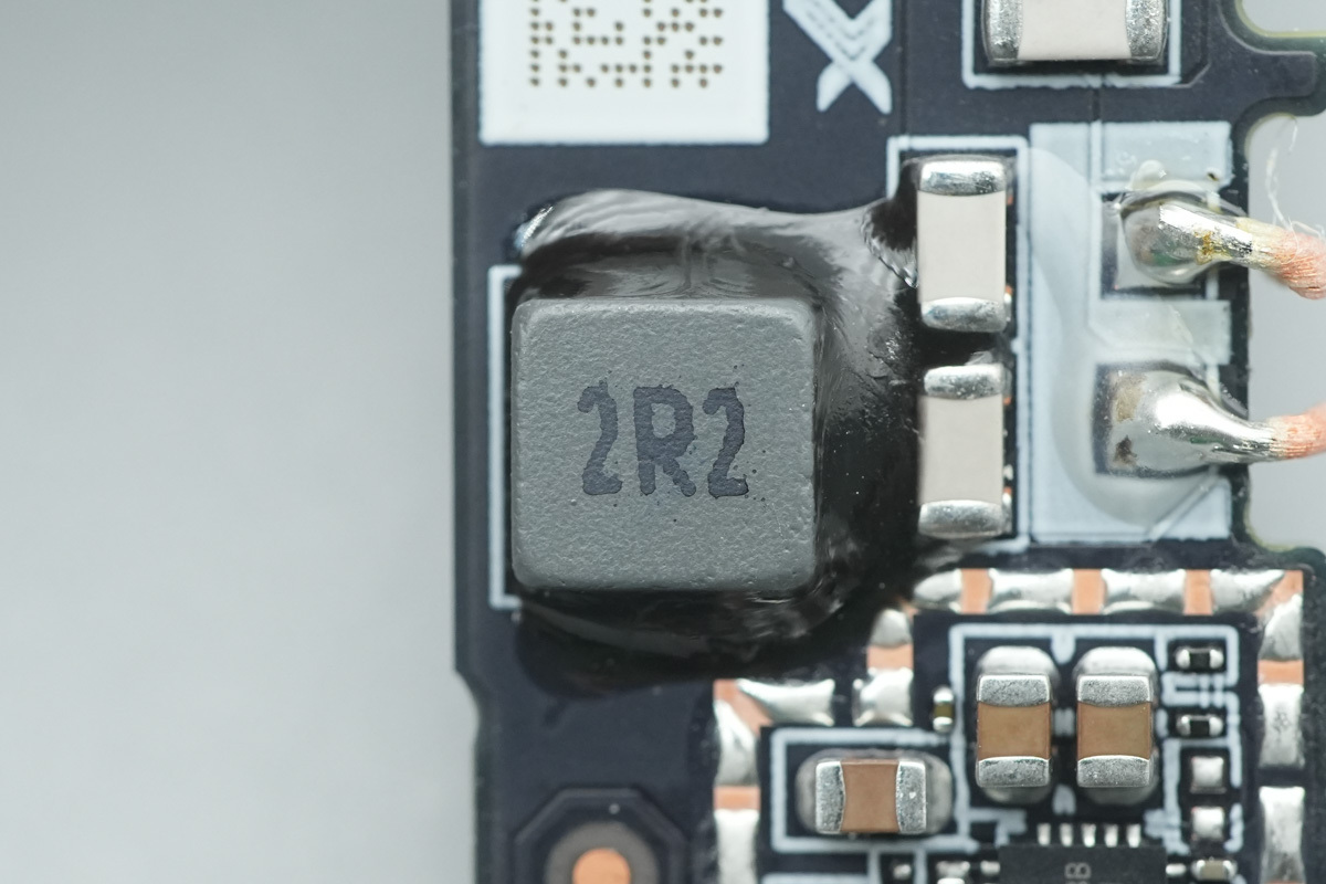
An alloy choke, 2.2μH.
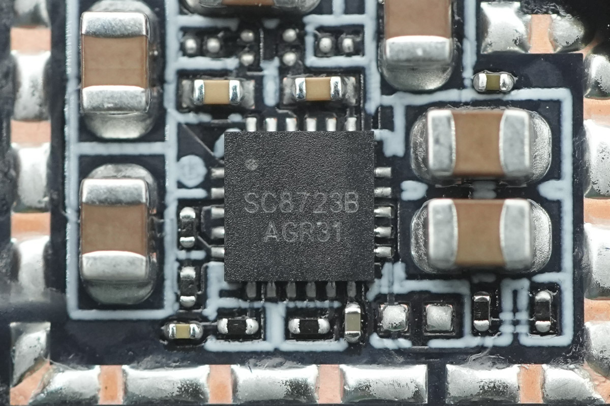
The synchronous buck-boost chip is from Southchip, model SC8723. It is a highly integrated four-switch synchronous buck-boost converter designed to provide high power efficiency and stable voltage regulation regardless of whether the output voltage is higher, lower, or equal to the input voltage.
The SC8723 supports a wide input and output voltage range: an input voltage range of 2.7V to 22V, an output voltage range of 3V to 22V, and a maximum output current of 3.5A.
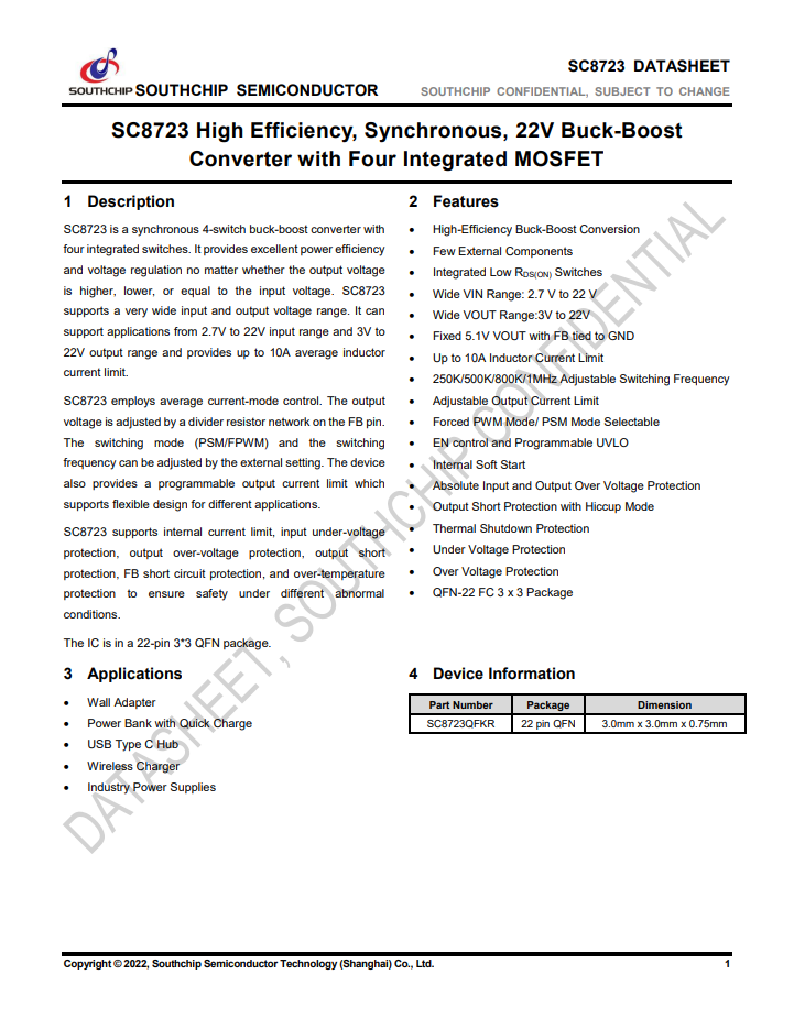
The SC8723 uses average current mode control. The output voltage is regulated via resistors on the FB pin. Both the operating mode (PSM/FPWM) and switching frequency are adjustable through external settings.
It offers programmable output current limiting, providing flexibility for various applications. Integrated safety features include internal current limiting, input UVLO, OVP, output SCP, FB short-circuit protection, and thermal shutdown, ensuring safety under various abnormal conditions, housed in a QFN22 package.
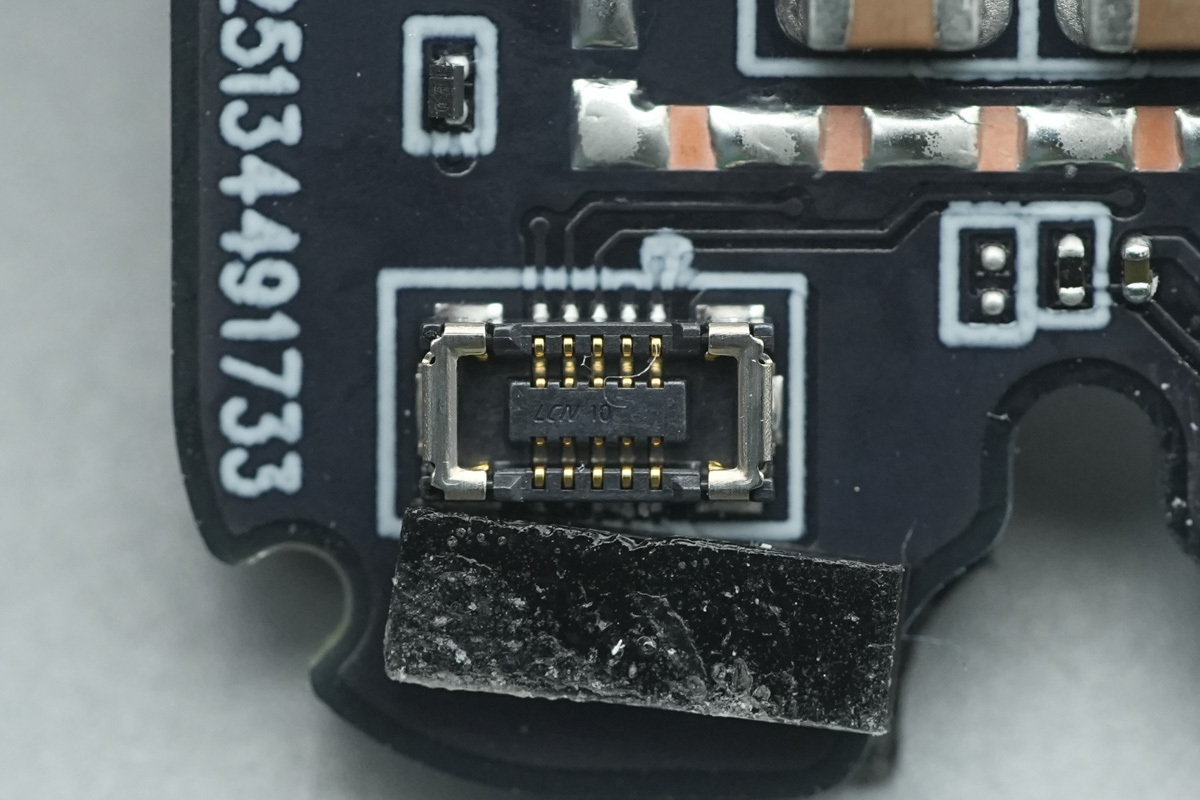
This is the BTB receptacle that links to the top PCB.
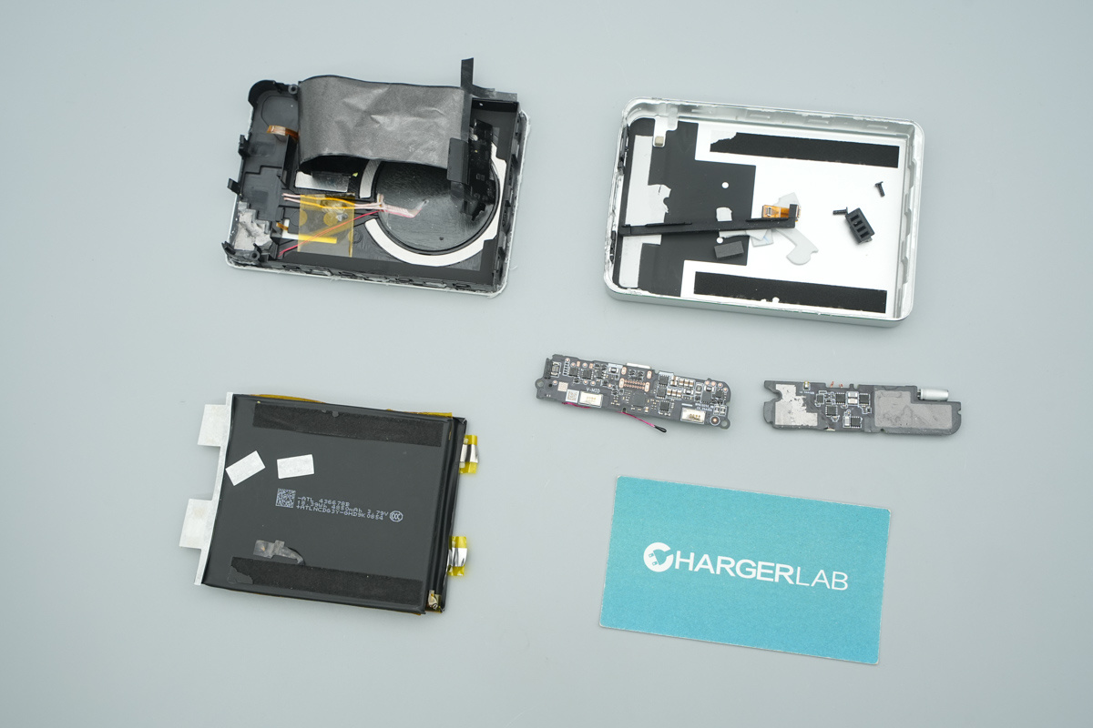
Well, those are all components of the Xiaomi Ultra Slim Power Bank 10,000mAh 45W.
Summary of ChargerLAB
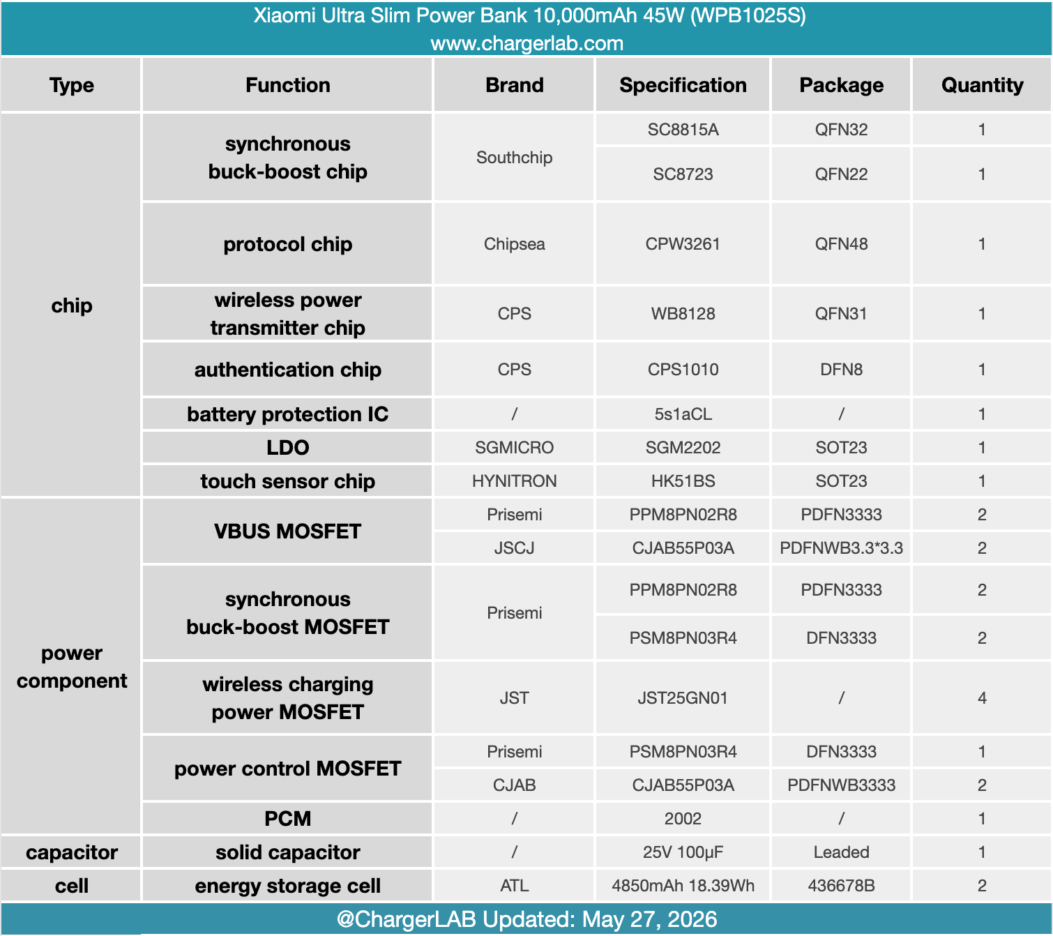
Xiaomi’s new 10,000mAh magnetic power bank strikes a perfect balance between performance and portability, delivering 45W wired and 20W wireless charging in a remarkably thin 13.20mm chassis.
Inside, it features a dual-cell battery configuration with high-density ATL lithium-polymer cells, highlighting professional-grade insulation and robust spot-welding. The electronics are arranged in a dual-layer, stacked PCB design linked by a flexible ribbon cable. The top PCB carries the Southchip bidirectional buck-boost chip, Chipsea protocol chip, and PCM, while the bottom board focuses on wireless charging, featuring a CPS transmitter and authentication chip driven by a Southchip buck-boost converter.
The build quality is exceptional, featuring a CNC-machined aluminum unibody, a reinforced USB-C port, and precision light-piped LED indicators. Thermal management is equally sophisticated, using extensive graphite heat-spreading sheets and dampening foam, plus dual NTC sensors to monitor temperature in real-time, ensuring safe, high-speed charging.
Related Articles:
1. Charging Compatibility Test of MIIIW 140W GaN Charger (Xiaomi Phones)
2. Teardown of Xiaomi 10000mAh Magnetic Power Bank (WPB1007ZX)
3. Teardown of Xiaomi 100W GaN Charger for Xiaomi 17 Series (MDY-18-EW)