
Introduction
In this episode, we take apart NVIDIA’s 800G dual-port OSFP optical transceiver (Model MMA4Z00). Equipped with dual 4-channel MPO-12/APC optical connectors and running on two 4-channel fibers, it utilizes 100G-PAM4 modulation to deliver up to 50 meters of reach while supporting both InfiniBand and Ethernet protocols.
Drawing power from a single 3.3V rail, it requires just 2W in low-power sleep mode and peaks at 17W under maximum load, driven by integrated 850nm VCSEL transmitters. Join Server Power Supply Net as we tear down this high-performance 800G OSFP module from NVIDIA to inspect its internal architecture and BOM.
Product Appearance
The NVIDIA optical transceiver is provided with original factory plastic packaging boxes.
Packaging Box Label Info:
Model: MMA4Z00
Part Number: MMA4Z00-NS
Country of Origin: Made in Malaysia
The front is equipped with cooling fins and an info label.
The back chassis is secured with screws.
Spring clips are provided on the side of the chassis.
The cooling fins on the front of the chassis.
A protective cover is provided at the front of the cooling fins to prevent contact with the internal PCB gold fingers.
The PCB gold fingers at the front of the module.
Model: MMA4Z00
Part Number: MMA4Z00-NS
OSFP 850nm 800Gbps up to 50M
Country of Origin: Made in Malaysia
A fiber optic connector is provided at the rear end of it.
The plastic mounting pull tab.
The back chassis is secured with screws.
Here are the screws fixing the housing.
A spring reset mechanism is provided inside the spring clip.
The length of the optical transceiver is about 115.4mm (4.543 inches).
The width of the optical transceiver is about 22.6mm (0.890 inches).
The thickness of the optical transceiver is about 14.5mm (0.571 inches).
That's how big it is in the hand.
The weight is about 112g (3.95 oz).
Teardown
With the unboxing complete, it’s time to tear down NVIDIA’s optical transceiver and inspect the engineering and BOM inside.
We start by removing the fixing screws and separating the chassis.
A rubber sealing ring is provided inside the chassis.
Conductive foam is provided inside the chassis corresponding to the optical fiber plug.
Thermal potting compound is applied to the chassis corresponding to the DSP chip.
The interior of the optical transceiver, with a fiber optic connector on the left and a PCBA on the right.
The fiber optic connector, with conductive foam shielding provided inside the chassis.
The optical fiber is connected to the optoelectronic module.
The optical fiber connector is connected to the VCSEL laser.
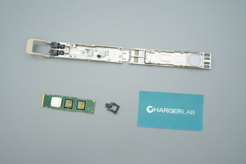
Remove the optical fiber connector and take out the PCBA from the chassis.
Thermal potting compound is applied inside the chassis corresponding to the heat-generating components.
The retention clips used for securing the optical fibers.
The front of the PCBA, featuring two VCSEL lasers on the left and a DSP chip on the right.
The left side of the back is equipped with an MCU, memory, a voltage comparator, a synchronous buck-boost chip, and a PMIC.
The DSP chip is from MARVELL, model IN080C0C, and is used for signal conditioning and driver functions.
The crystal oscillator providing the clock signal for the DSP chip.
The memory, marked V40L.
The two VCSEL lasers, which together form an 800Gbps bandwidth.
The MCU is from ST, model STM32L452REY8, featuring an embedded Arm Cortex-M4 MCU with FPU, 80MHz operating frequency, DSP instructions, 512KB Flash memory, and 160KB SRAM. It supports a 1.71-3.6V operating voltage and utilizes a WLCSP64 package.
The memory is from GIANTEC, marked 58, and in an UDFN package.
The chip, marked d5.
The PMIC is from RENSEAS, marked BR5930.
The voltage comparator is from 3PEAK, marked 962, model TP1962, which is a low-power, ultra-fast dual voltage comparator supporting 3V and 5V applications in a DFN2*2-8 package.
The synchronous buck-boost chip is from MPS, marked ANA, model MP28164. It is a high-efficiency single-choke synchronous buck-boost converter with integrated switching MOSFETs, utilizing a fixed-frequency PWM current control mode with a 2MHz switching frequency. It supports an input voltage range of 1.2-5.5V and an output voltage range of 1.5-5V, housed in a QFN-11 package.
The external alloy choke associated with the chip.
The synchronous step-down chip, marked M4FTJ, and is housed in a SOT563 package.
The step-down choke used in conjunction with the IC.
The load switch is from Silergy, marked Wd, model SY6210. It is a 2.5-5.5V 10A current load switch with an integrated ultra-low on-resistance switching MOSFET, utilizing a DFN2*3-10 package.
Here is the chip, marked L8K NP.
The chip, marked 8P Ns.
Buffer rubber pads are provided on the edge of the PCBA.
The gold fingers for the optical transceiver connection.
Well, those are all components of the NVIDIA 800G Dual-Port OSFP Optical Transceiver MMA4Z00-NS.
Summary of ChargerLAB
NVIDIA's 800G dual-port OSFP optical transceiver is housed in a screw-secured metal chassis complete with integrated heat sinks. Carrying the MMA4Z00 part number, the transceiver packs dual 4-channel MPO-12/APC optical interfaces driven by 100G-PAM4 modulation over two 4-channel fiber links, delivering robust 50-meter reach.
Disassembly reveals a high-density internal PCBA powered by MARVELL's IN080C0C DSP and ST's STM32L452REY8 MCU, energized via RENSEAS PMIC solutions. Circuit protection and power regulation are further reinforced by a Silergy SY6210 load switch, MPS MP28164 buck-boost converter, and 3-Peak TP1962 high-speed comparator.
Thermal potting compound coats all primary hot spots across the PCB and behind the VCSEL diodes, transferring heat directly to the exterior shell. Internally, conductive foam lines the fiber interface zones for reliable EMI shielding, while snap-in latches lock the optical connectors firmly in place against vibration or pulls.
Related Articles:
1. Teardown of the NVIDIA DGX Spark Original 240W USB-C Power Adapter
2. Navitas Selected for NVIDIA’s Next-Gen 800V HVDC Data Center Architecture
3. ChargerLAB POWER-Z Fan Test: NVIDIA DGX Supports 240W PD 3.1 Power Delivery