Introduction
TRANSSION owns brands such as TECNO, itel, and Infinix. Recently, we got our hands on the TECNO INBOX standard 45W charger. This charger is the European version, supporting 100–240V AC input and 11V⎓4.1A output, with a maximum power output of 45W. Let’s take a closer look at the internal design and components of this charger.
Product Appearance
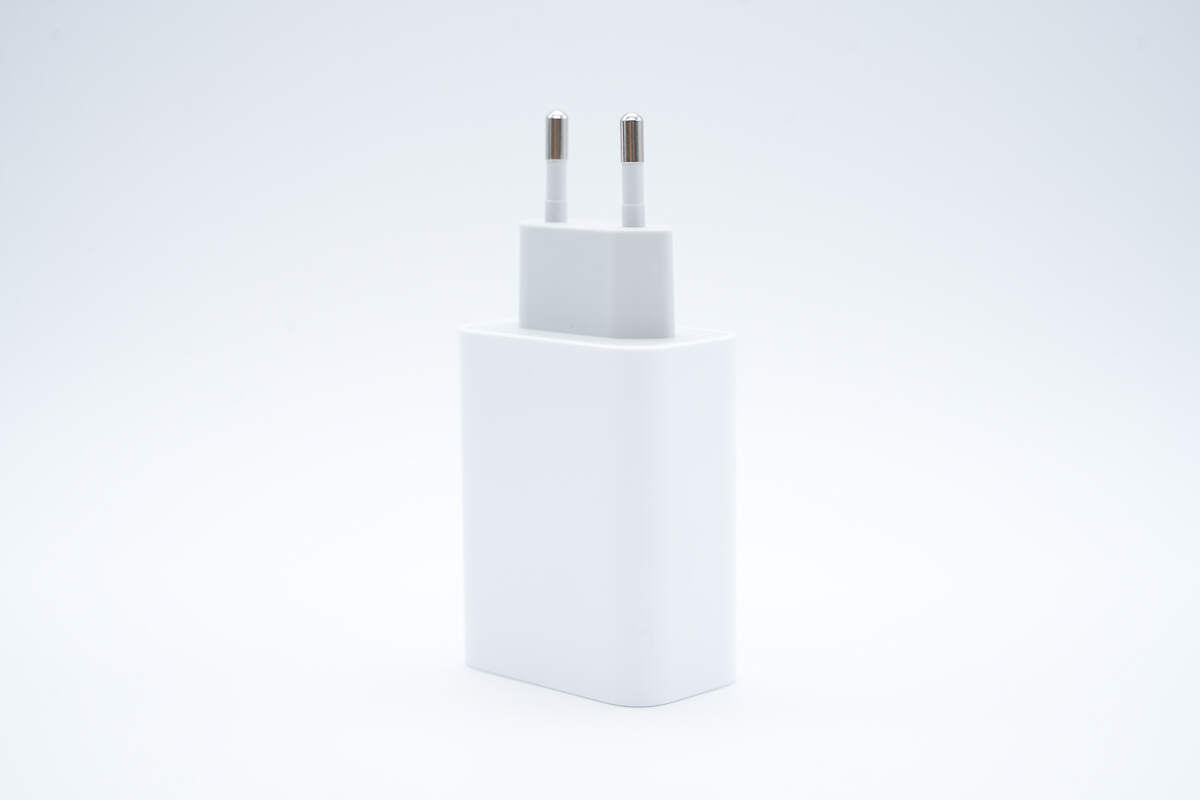
The outer shell is made of flame-retardant material.
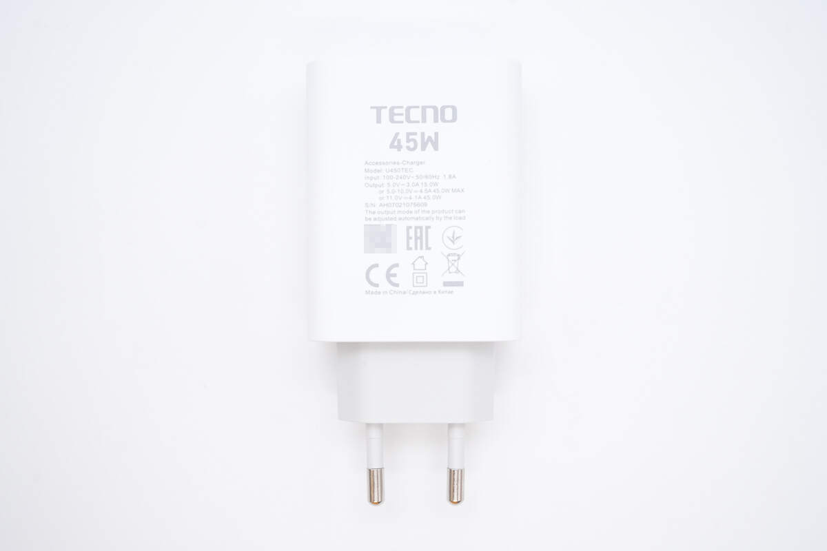
The back is printed with specification information.
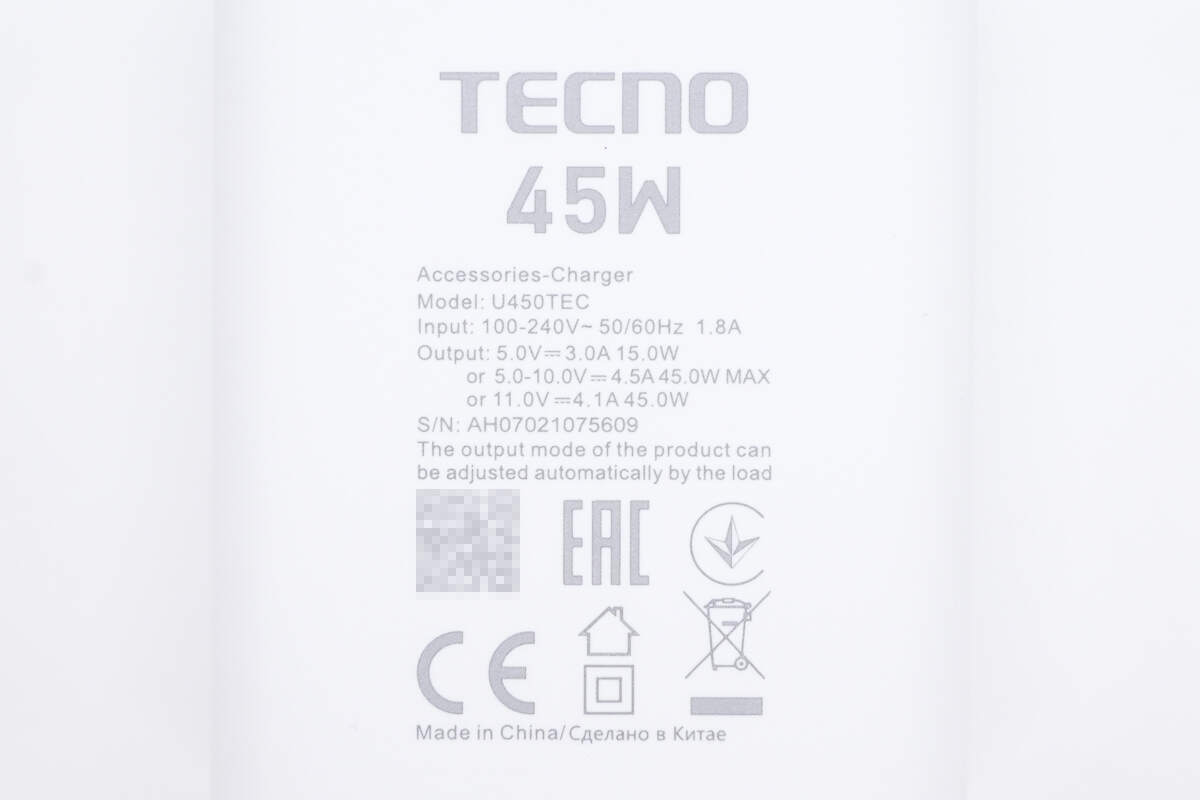
Model: U450TEC
Input: 100-240V\~50/60Hz 1.8A
Output: 5V3A 15W
or 5-10V4.5A 45W MAX
or 11V4.1A 45W
Certified by CE and EAC.
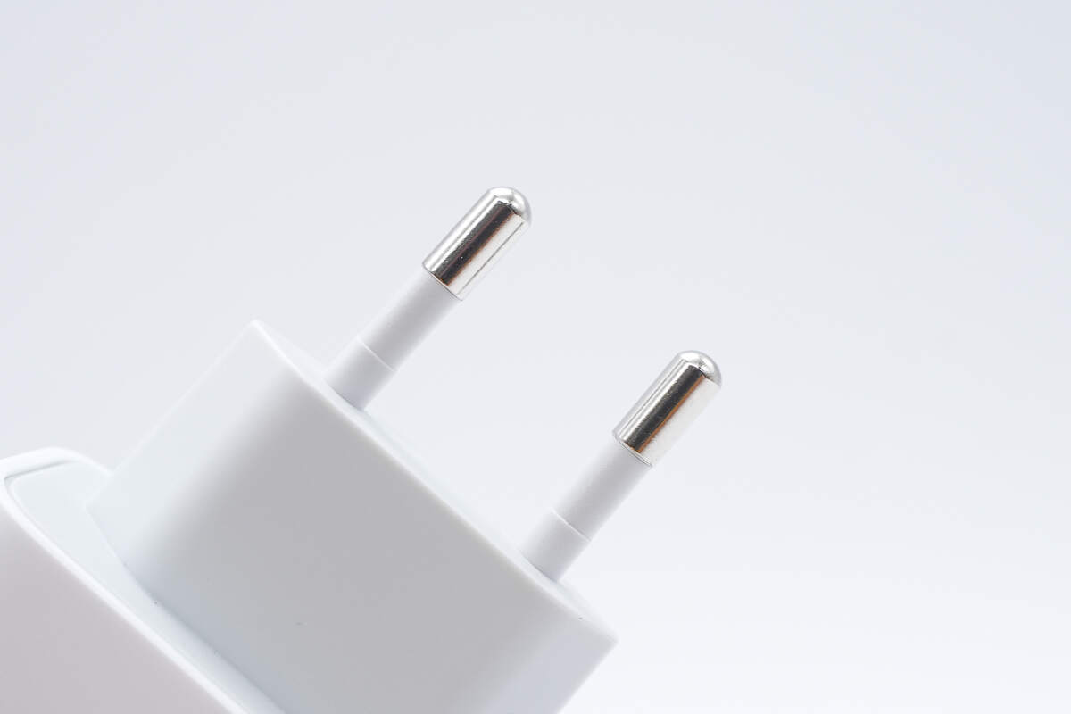
Equipped with European standard prongs.
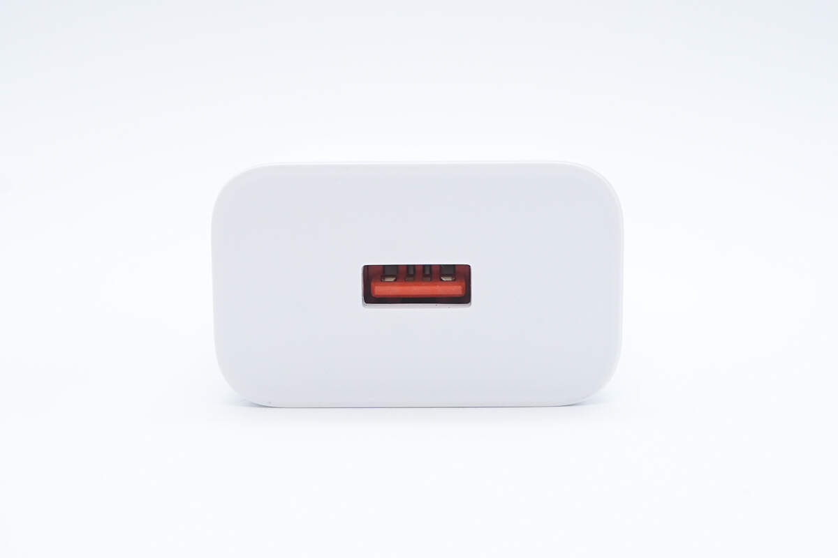
The plastic sheet of the USB-A is orange.
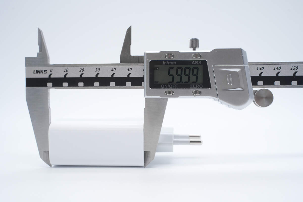
The length is about 59.99 mm (2.36 inches).
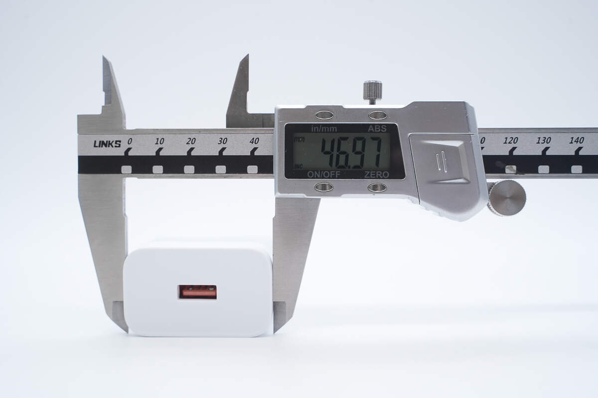
The width is about 46.97 mm (1.85 inches).
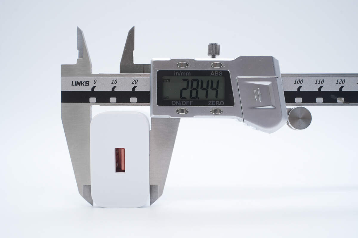
The thickness is about 28.44 mm (1.12 inches).
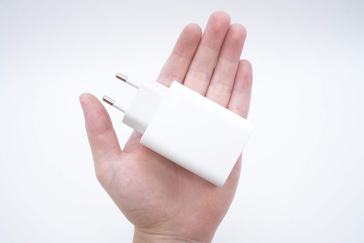
That's how big it is in the hand.
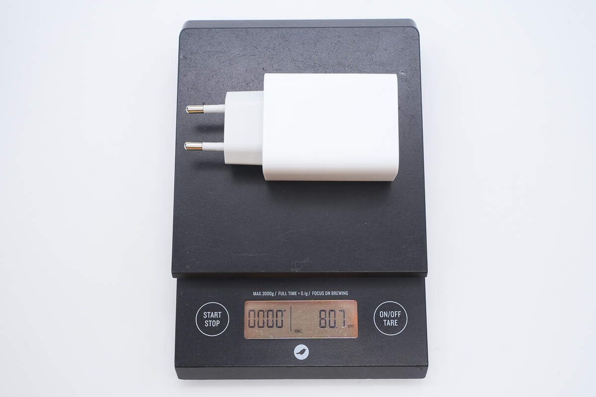
The weight is about 81 g (2.86 oz).
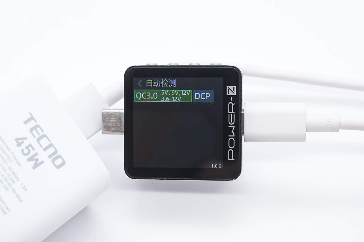
ChargerLAB POWER-Z KM003C shows that it supports the QC3.0 and DCP charging protocols.
Teardown
Next, let's take it apart to see its internal components and structure.
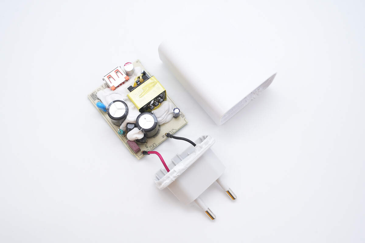
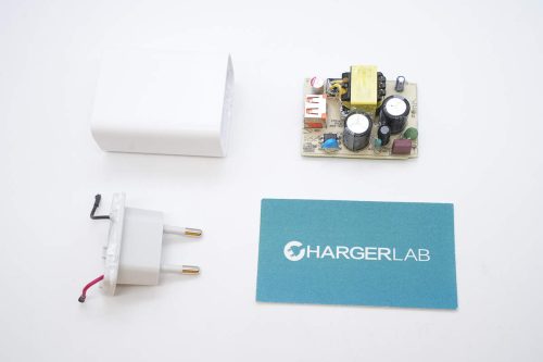
Disassemble the input end casing and remove the PCBA module.
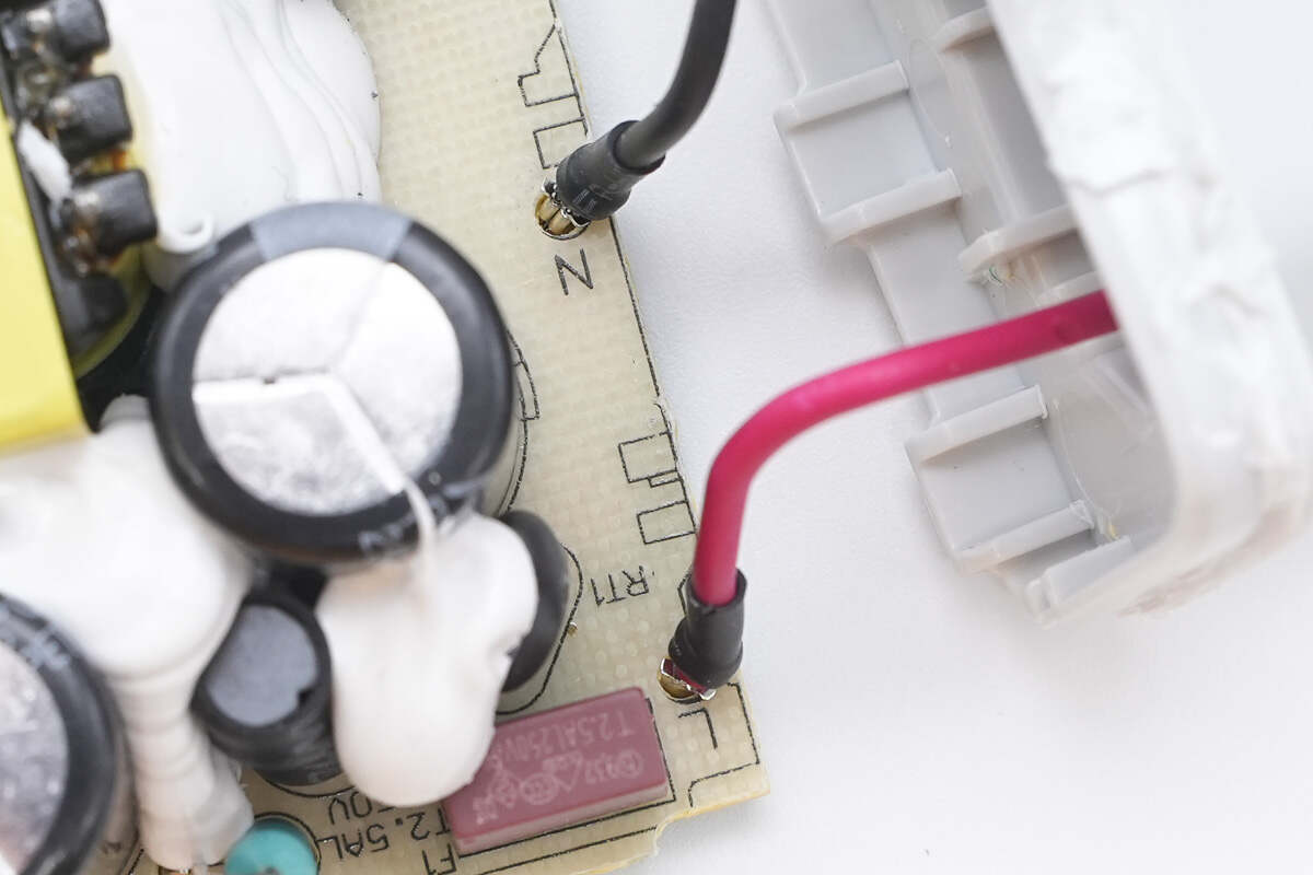
The prongs are connected to the PCBA module by wires.
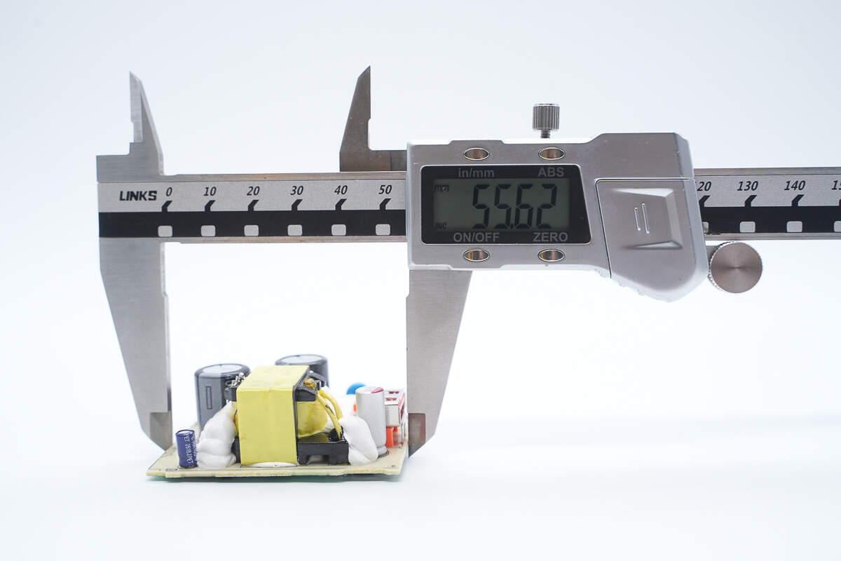
The length of the PCBA module is about 55.62 mm (2.19 inches).
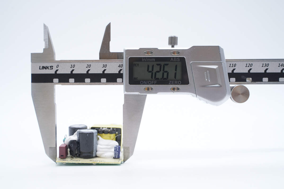
The width is about 42.61 mm (1.68 inches).
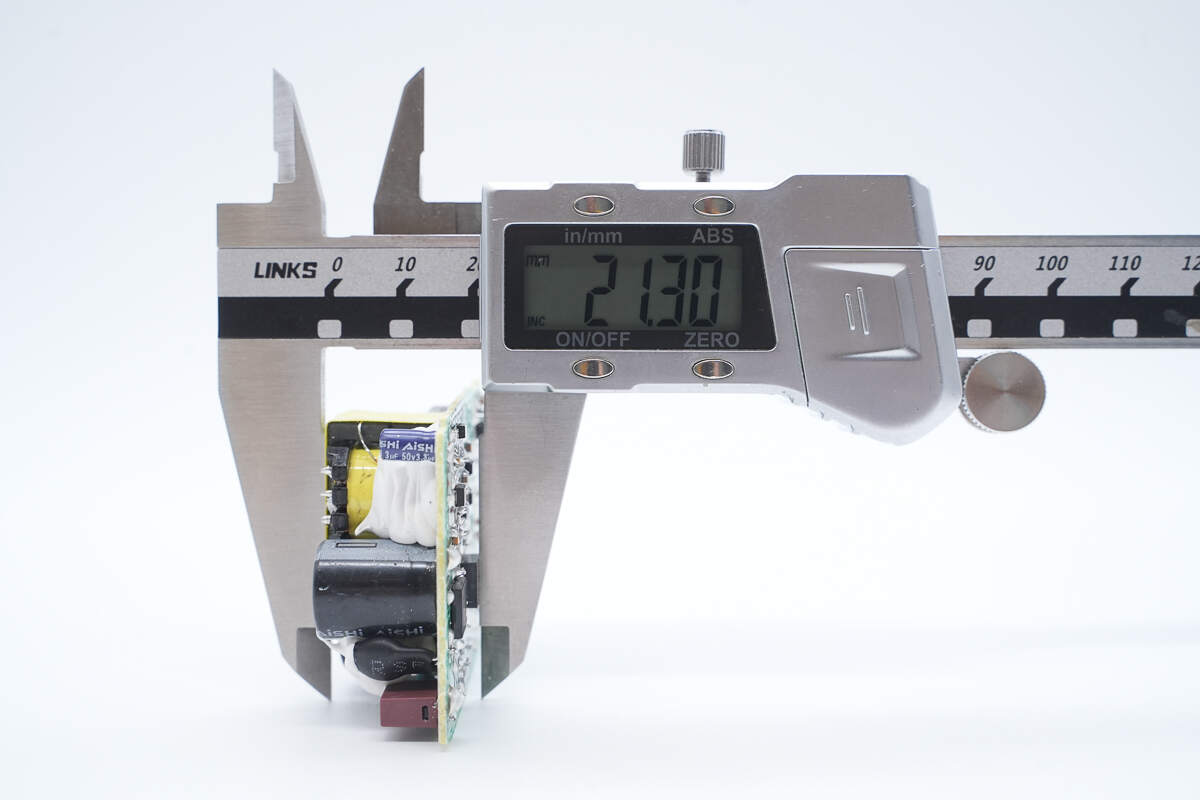
The thickness is about 21.3 mm (0.84 inches).
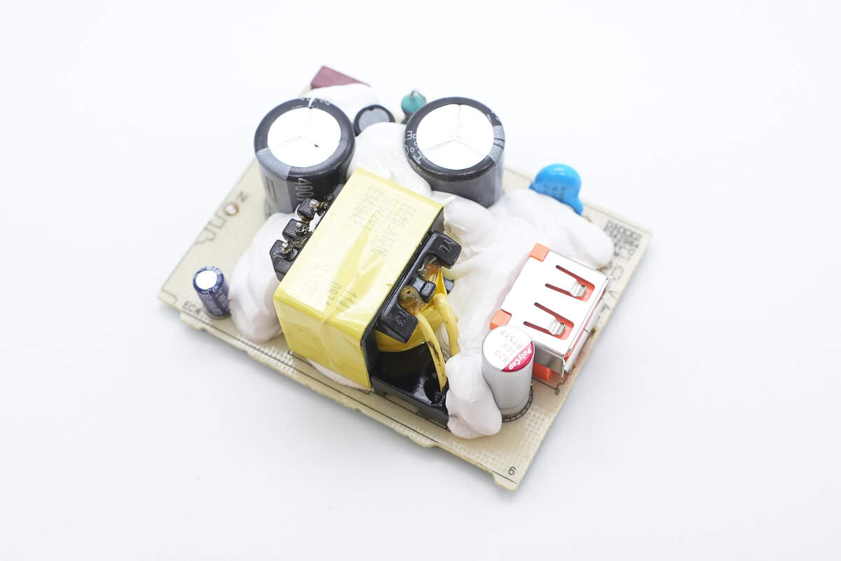
The PCBA is single-sided printed. Components such as the transformer are reinforced with white adhesive.
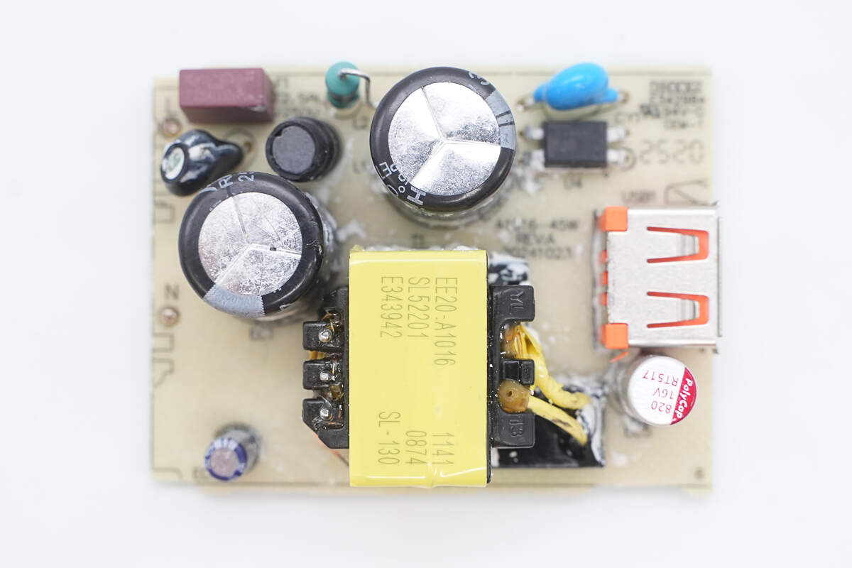
Clean off the white adhesive. The front side of the PCB has components such as a time-delay fuse, an I-shaped inductor, electrolytic capacitors, and a transformer.
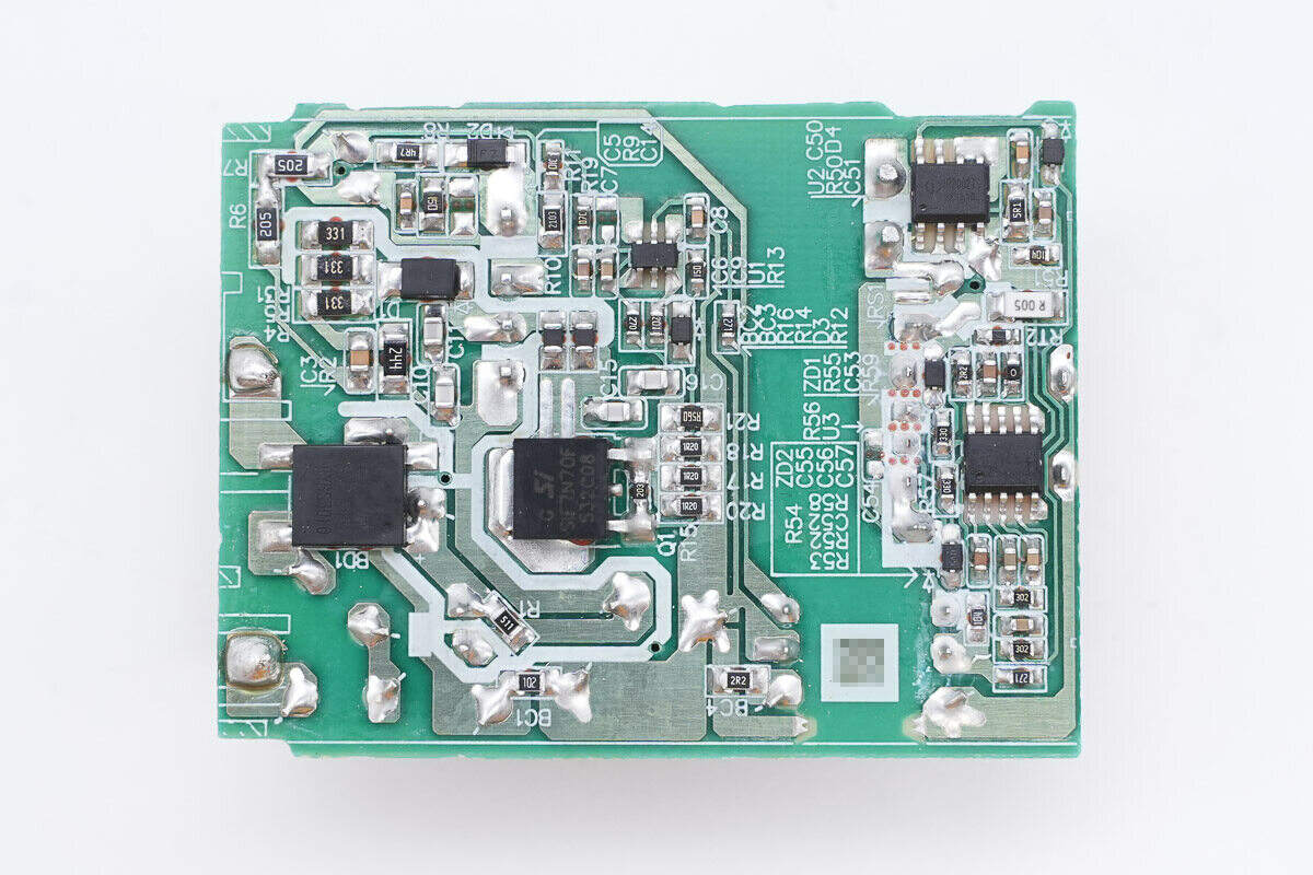
The back side has a bridge rectifier, primary master control chip, primary MOSFET, synchronous rectifier controller, and protocol chip.
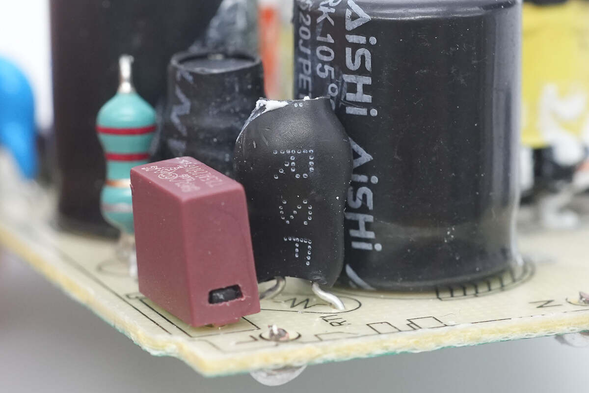
At the front end of the module, you can see the time-delay fuse, NTC thermistor, I-shaped inductor, and electrolytic capacitors.
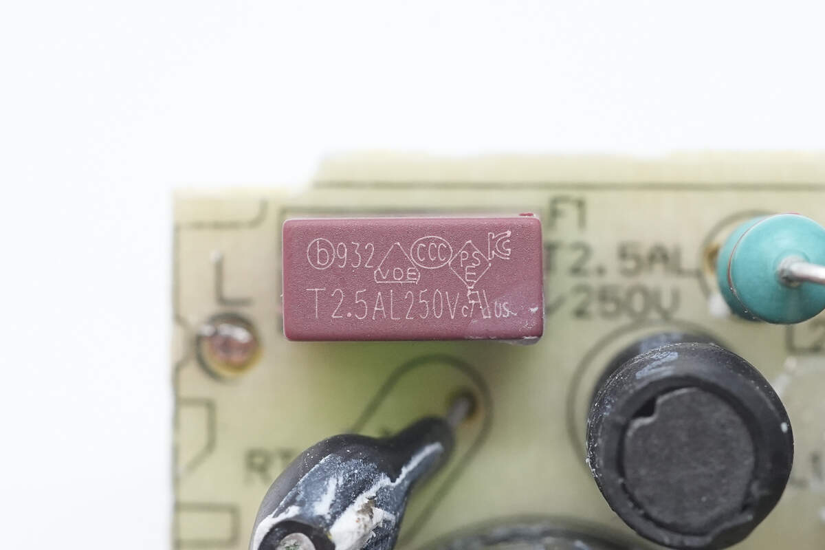
The time-delay fuse is from Betterfuse, part number 932, rated at 2.5A 250V.
The NTC thermistor is insulated with a heat-shrink tube.
The NTC thermistor is used to suppress inrush current during power-up.
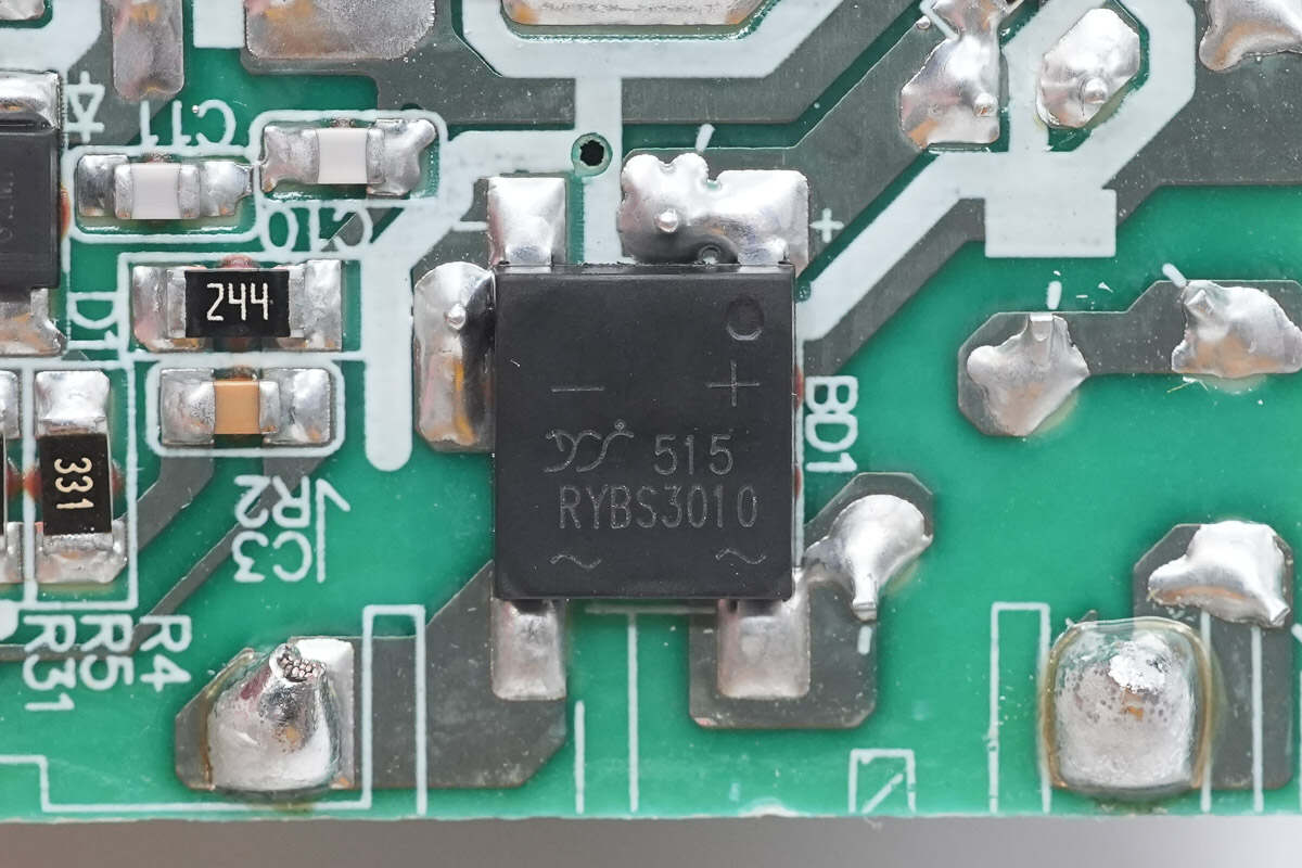
The bridge rectifier is from YJ, model RYBS3010. It is a fast-recovery bridge rectifier rated at 3A 1000V, using a YBS package.
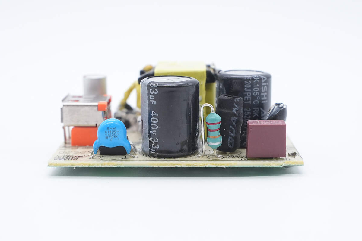
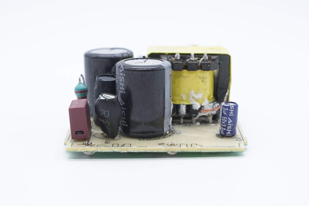
On the side, you can see a color-ring inductor, an I-shaped inductor, and electrolytic capacitors.
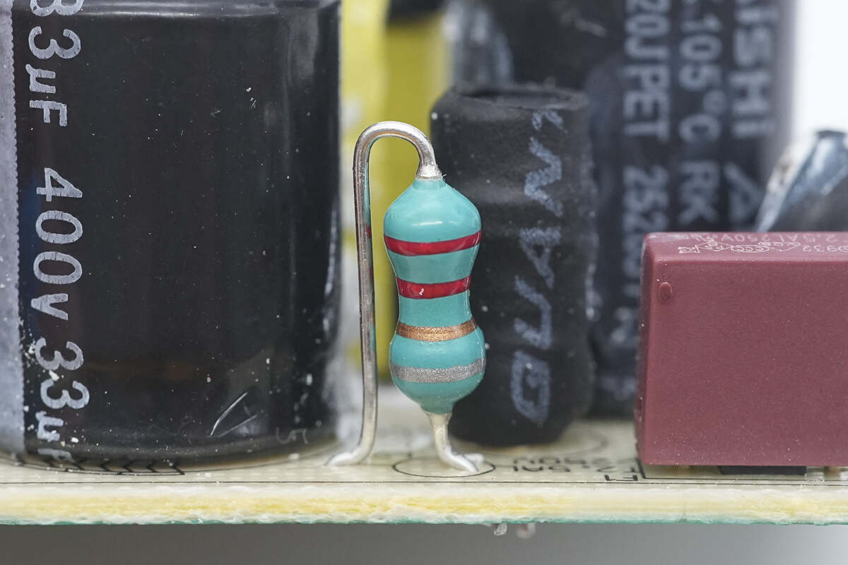
Close-up of the color-ring inductor.
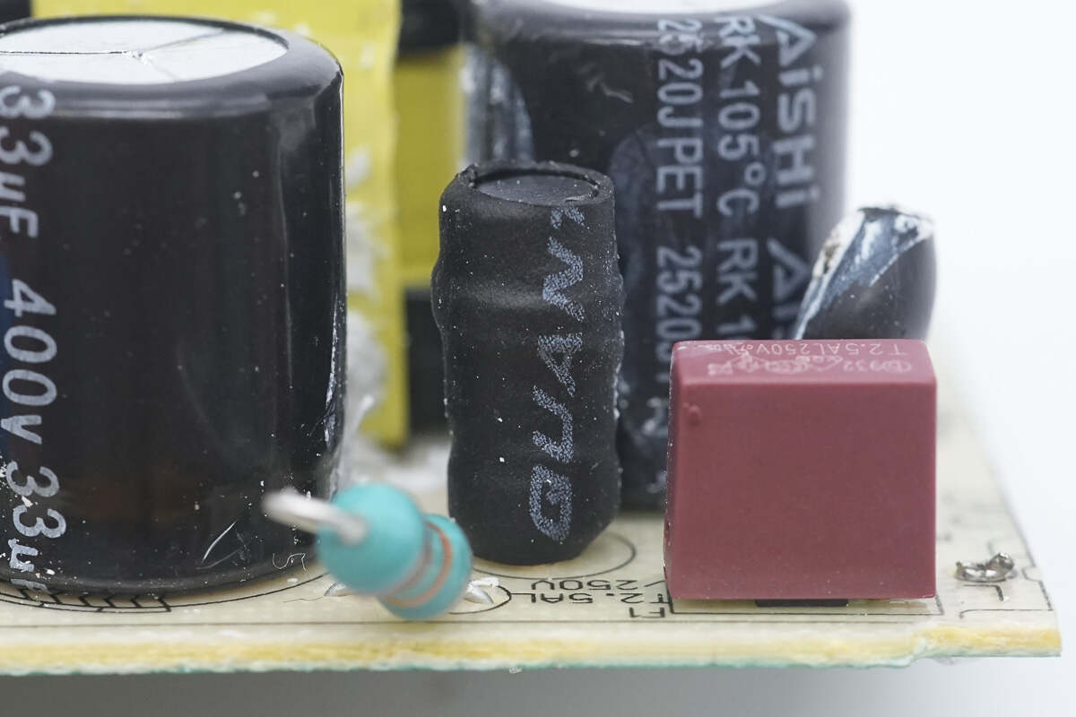
The I-shaped filter inductor is insulated with a heat-shrink tube.
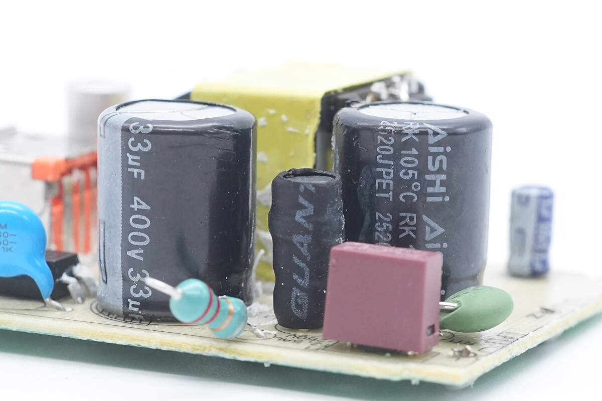
The two electrolytic capacitors are from AiSHi, both rated at 400V 33μF.
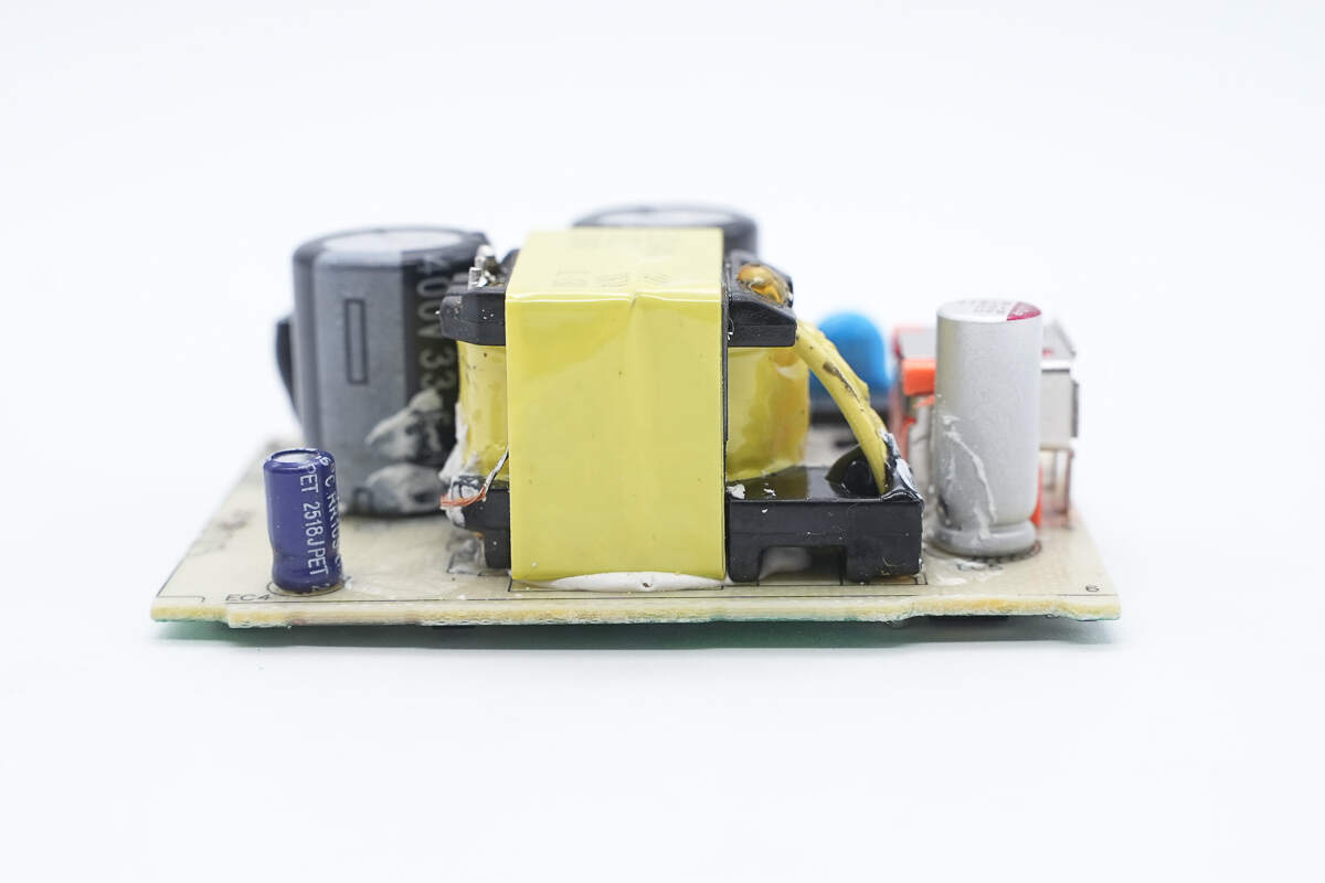
On this side, you can see the capacitor that supplies power to the master control chip, as well as the transformer.
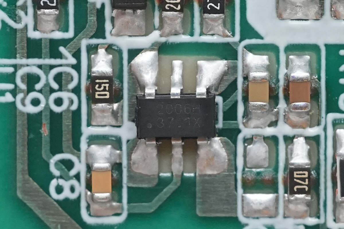
The primary master control chip is from Injoinic, model IP2006H. It is a high-performance multi-mode flyback controller featuring frequency foldback and valley switching technologies. It supports adaptive switching frequency to improve light-load efficiency, optimizes maximum switching frequency to reduce temperature rise, and enhances full-load efficiency.
It has burst mode operation to lower standby power consumption under light and no-load conditions, meeting CoC V5 and DoE VI standards. The chip includes comprehensive protection functions such as Brown-in/Brown-out, output over-voltage protection, output under-voltage protection, VDD over-voltage protection, input over-voltage protection, and over-temperature protection. It also supports customizable parameters and over-power protection. The package type is SOT23-6.
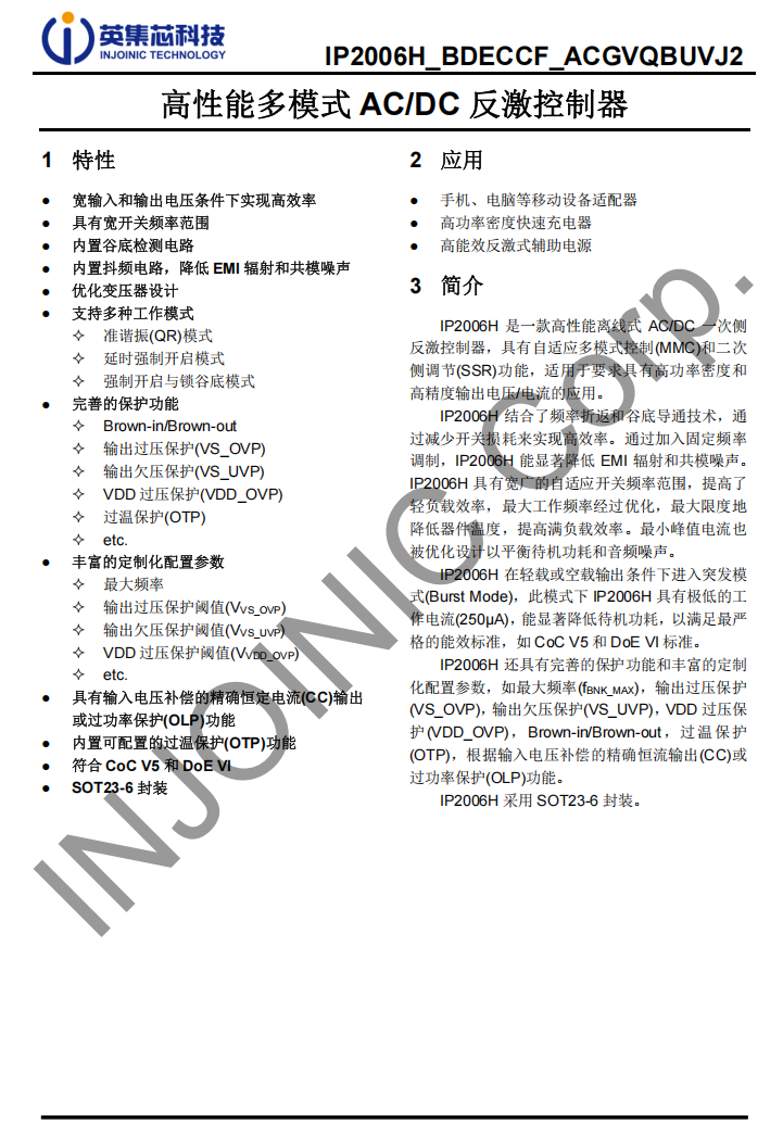
Here is the information about Injoinic IP2006H.
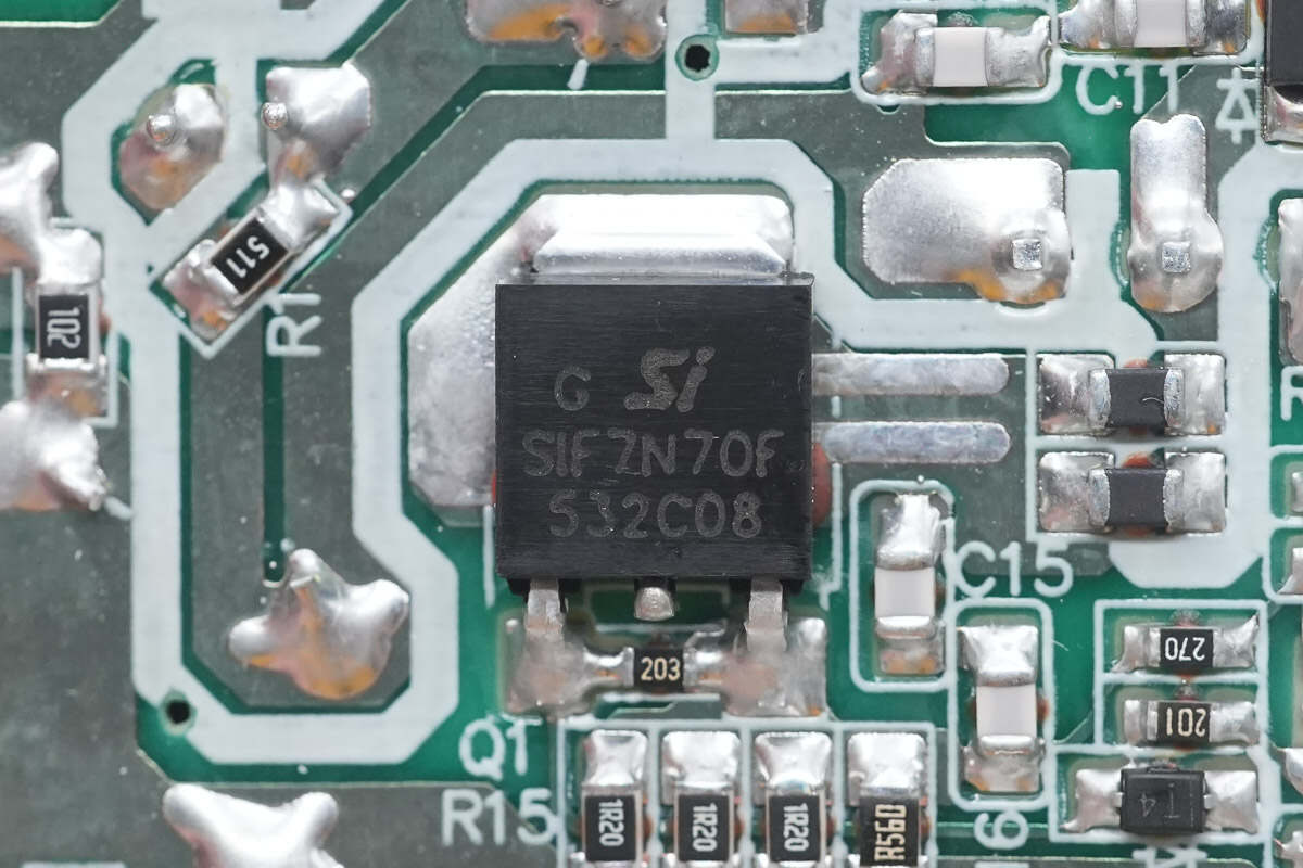
The primary MOSFET is from SI, model SIF7N70F. It is an N-channel MOSFET with a voltage rating of 700V and an on-resistance of 0.96Ω, housed in a TO-252T package.
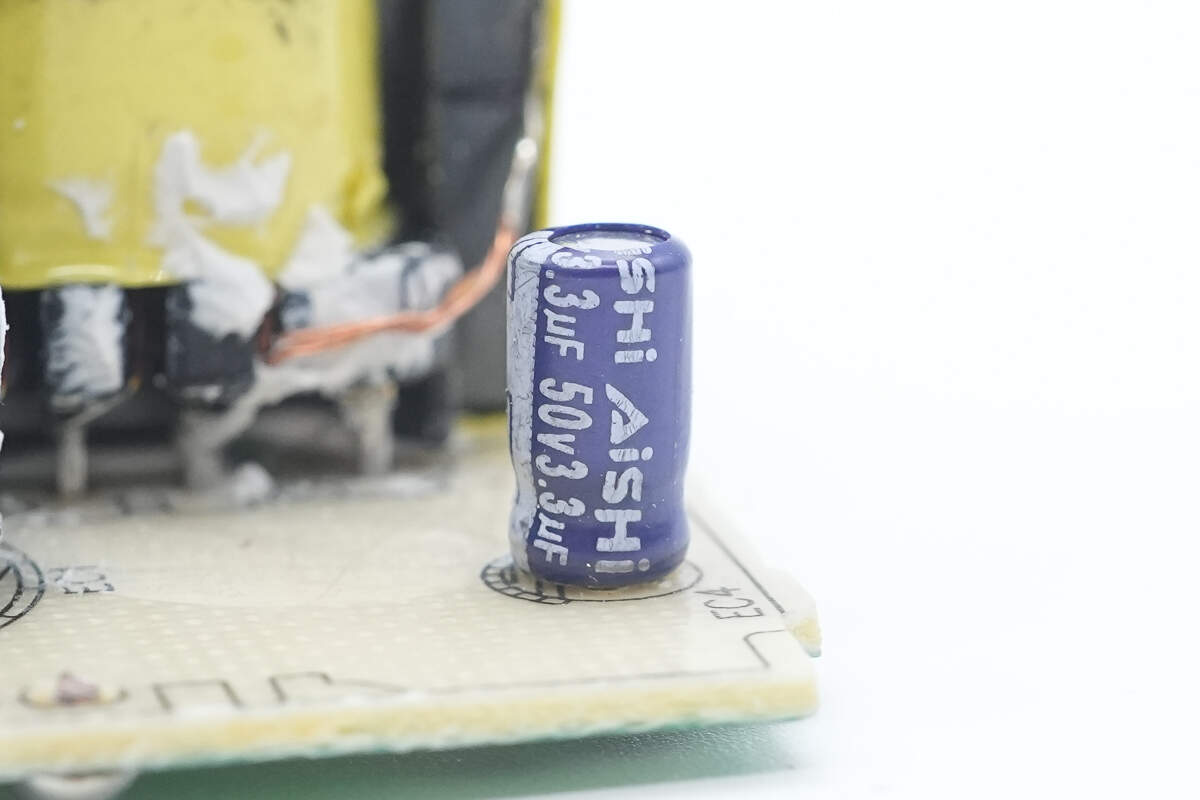
The capacitor that supplies power to the master control chip is also from AiSHi, rated at 50V 3.3μF.
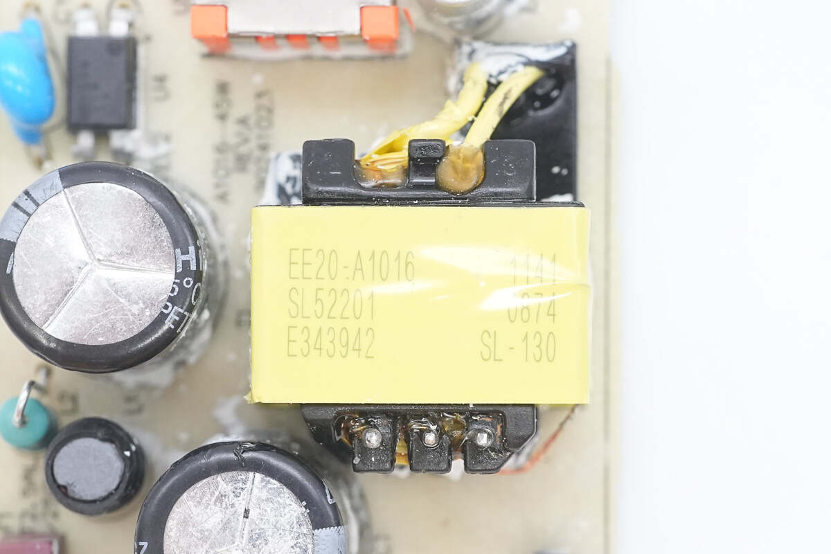
Close-up of the transformer.
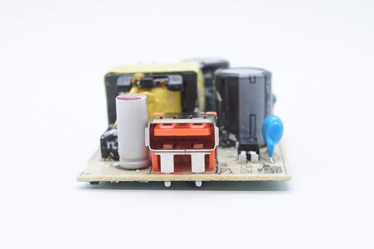
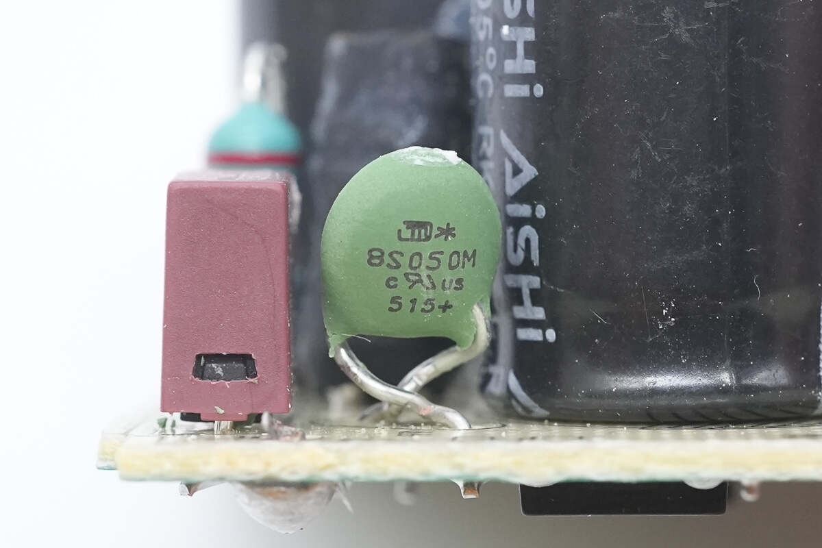
The output end features a USB-A socket, an optocoupler, a blue Y capacitor, and a solid capacitor.
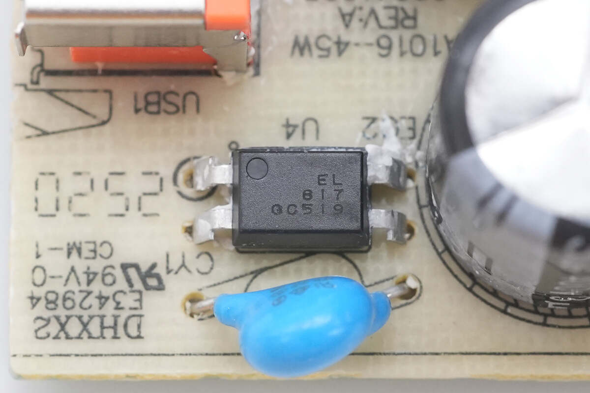
The Everlight EL817 optocoupler is used for output voltage feedback.
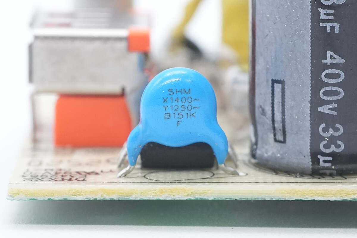
Close-up of the blue Y capacitor.
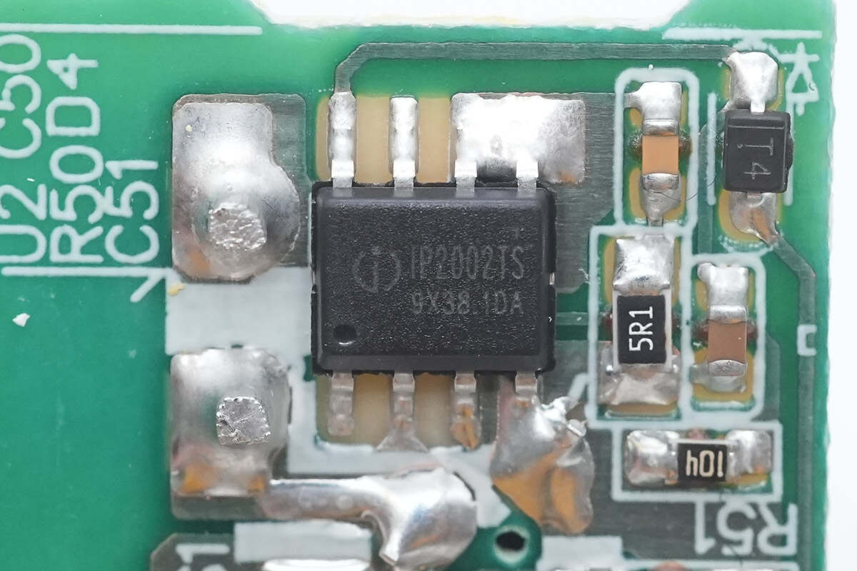
The synchronous rectifier controller is from Injoinic, model IP2002TS. It integrates a 65V MOSFET and can replace the Schottky diode rectifier in high-efficiency flyback power supplies. By detecting the drain-to-source voltage of the SR MOSFET, the IP2002TS can output optimal drive signals to turn the MOSFET on or off. This effectively reduces the power loss of the secondary-side rectifier, achieving higher efficiency and greater power density.
With minimal external components, it provides a high-performance solution for output voltages ranging from 3.3V to 12V. It does not require an auxiliary winding for power supply, as the internal voltage regulator generates its power voltage. This makes it suitable for charger applications with low output voltage requirements or adapters using a high-side synchronous rectification scheme.
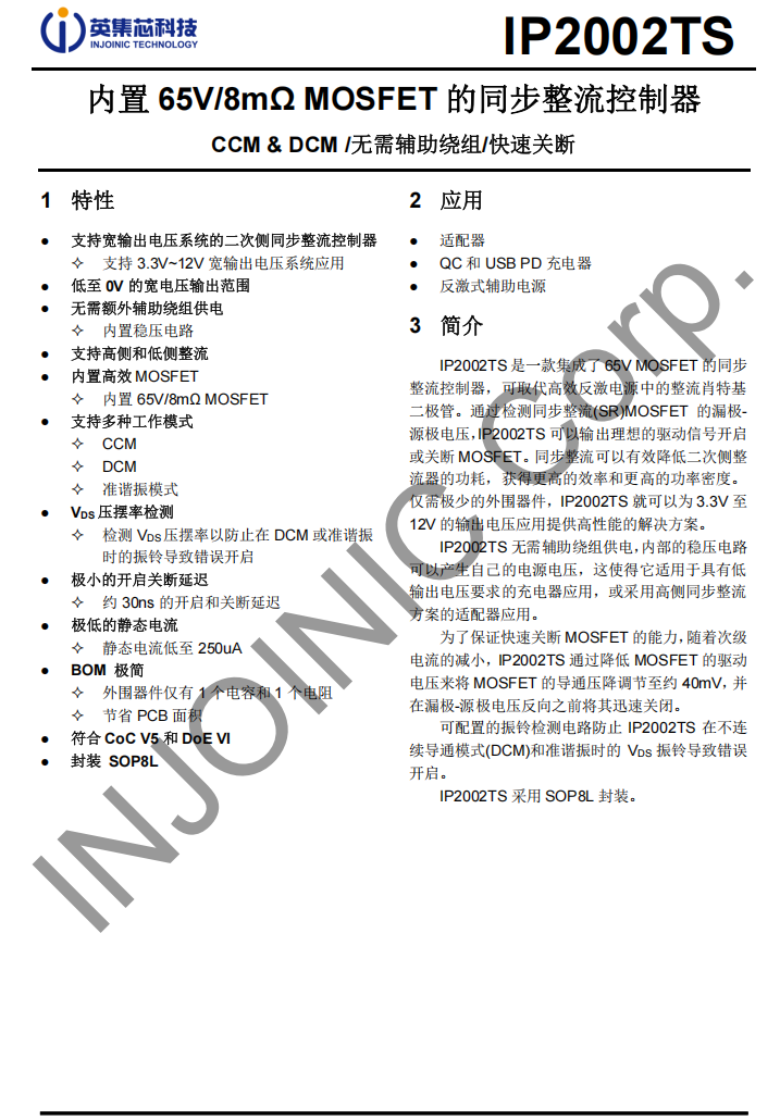
To ensure the ability to quickly turn off the MOSFET, as the secondary current decreases, the IP2002TS reduces the MOSFET’s drive voltage to adjust the conduction voltage drop to approximately 40mV. It rapidly turns it off before the drain-to-source voltage reverses. A configurable ringing detection circuit prevents false turn-on of the IP2002TS caused by V\_DS ringing during DCM and quasi-resonant operation. The IP2002TS comes in an SOP8L package.
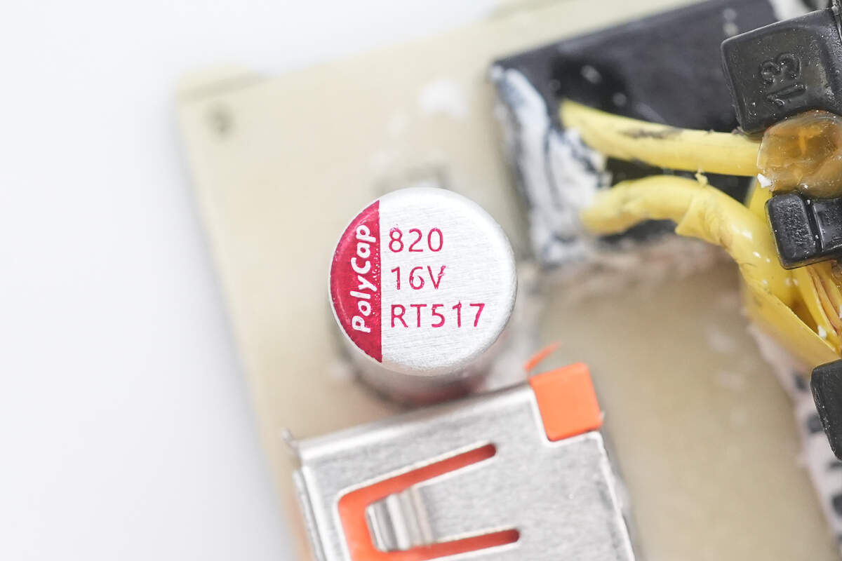
The solid capacitor is from PolyCap. 16V 820μ.
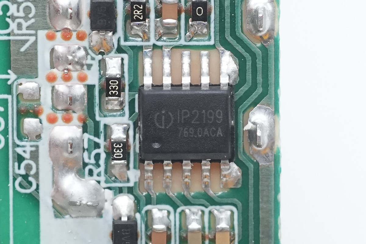
The protocol chip is from Injoinic, model IP2199. It supports the TFCP fast charging protocol as well as the BC1.2 charging standard. It automatically detects the charging protocol of the connected device and responds to fast charging requests according to the protocol standards. The IP2199 provides a complete TFCP fast charging solution for applications such as adapters, power banks, and car chargers.
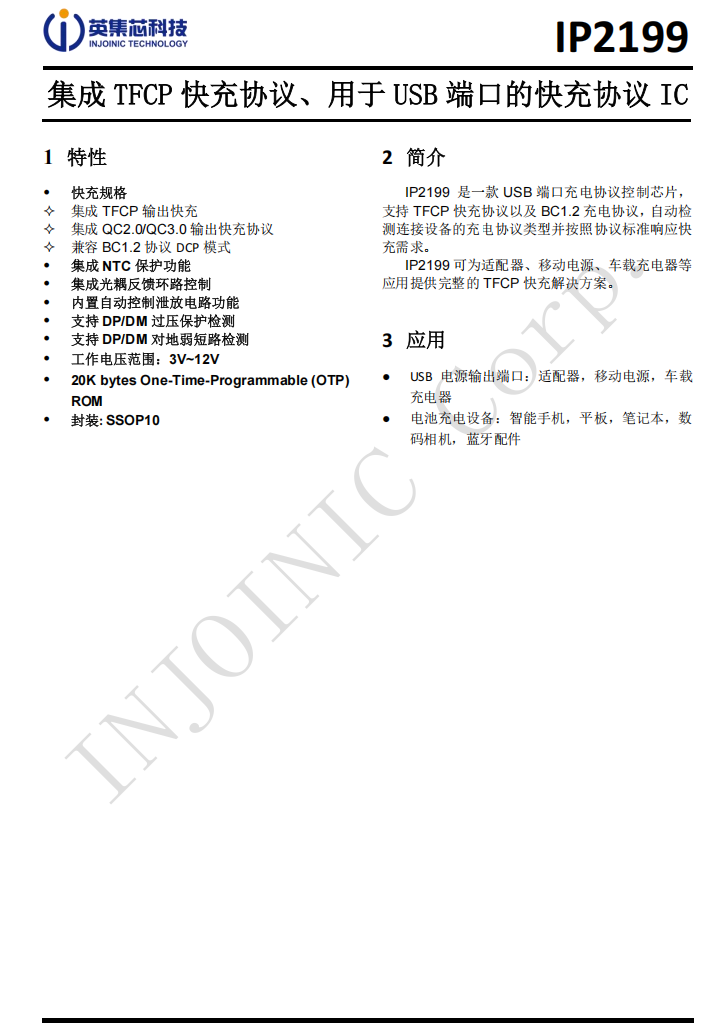
Here is the information about Injoinic IP2199.
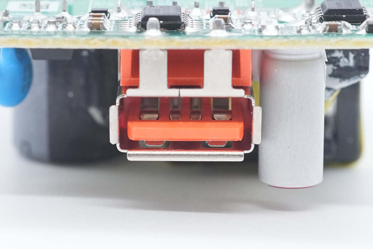
Close-up of the USB-A socket.

Well, those are all components of the TECNO 45W Accessories Charger.
Summary of ChargerLAB
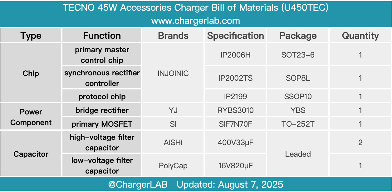
Here is the component list of the TECNO 45W Accessories Charger for your convenience.
It is equipped with European standard prongs and a USB-A output port, supporting a wide input voltage range of 100–240VAC. With the appropriate adapter, it can be used in most countries and regions worldwide. It supports outputs of 5–10V at 4.5A and 11V at 4.1A, with a maximum output power of 45W.
After taking it apart, we found that it is designed based on the Injoinic IP2006H + IP2002TS solution and also uses the Injoinic IP2199 protocol chip to implement output control. The solution has a high level of integration and good consistency. It uses capacitors from two well-known brands, AiSHi and PolyCap, for filtering. The components are reinforced with adhesive, and the overall build quality and materials are quite good.
Related Articles:
1. Teardown of Insta360 X5 Utility Fast Charge Case (CINSBAHM)
2. Teardown of Zhizu 2700Wh Zhiba MAX LiFePO₄ Swappable Battery Pack (DM60N-45ET)
3. Teardown of Dyson Supersonic r 1700W hair dryer (HD17)