Introduction
We have procured a GaN power amplifier released by SMSL, model PA200. It features a full aluminum alloy chassis, a front display with a function knob, and an infrared remote control for convenient volume adjustment. The rear panel includes audio input jacks, speaker outputs, and a power input connector.
The unit integrates a high-power dedicated switching power supply and Infineon GaN FETs, and incorporates over-temperature and over-current protection circuits. It supports both mono bridged mode and stereo mode. In mono mode, it delivers 250Wrms into an 8-ohm load, while in stereo mode it outputs 85Wrms per channel into 8 ohms.
Compared with traditional silicon devices, GaN semiconductors offer higher switching speeds, reduced dead time, and higher modulation frequencies in digital amplifiers. This enables GaN-based digital power amplifiers to achieve lower distortion, wider frequency response, and greater dynamic range. The following teardown examines the internal design and components of this SMSL GaN power amplifier.
Product Appearance

It comes in a cardboard box printed with the brand name, model designation, and an image of the product.

Accessories include a power cord, user manual, warranty card, and remote control.
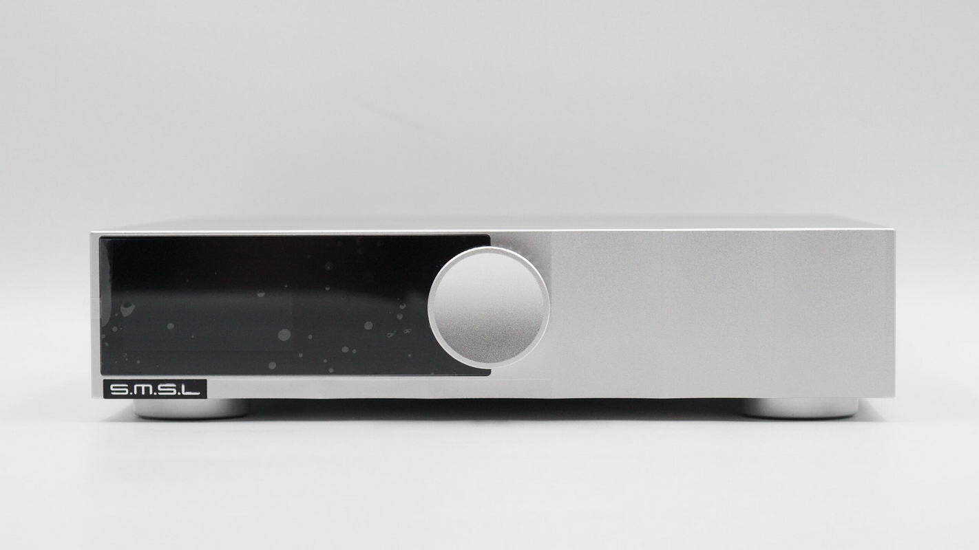
On the front panel, a display is positioned on the left side, and a volume control knob is located in the center.
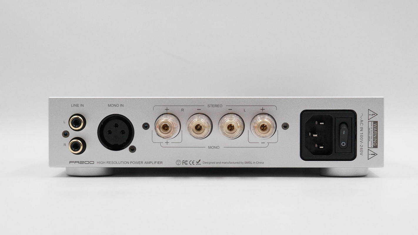
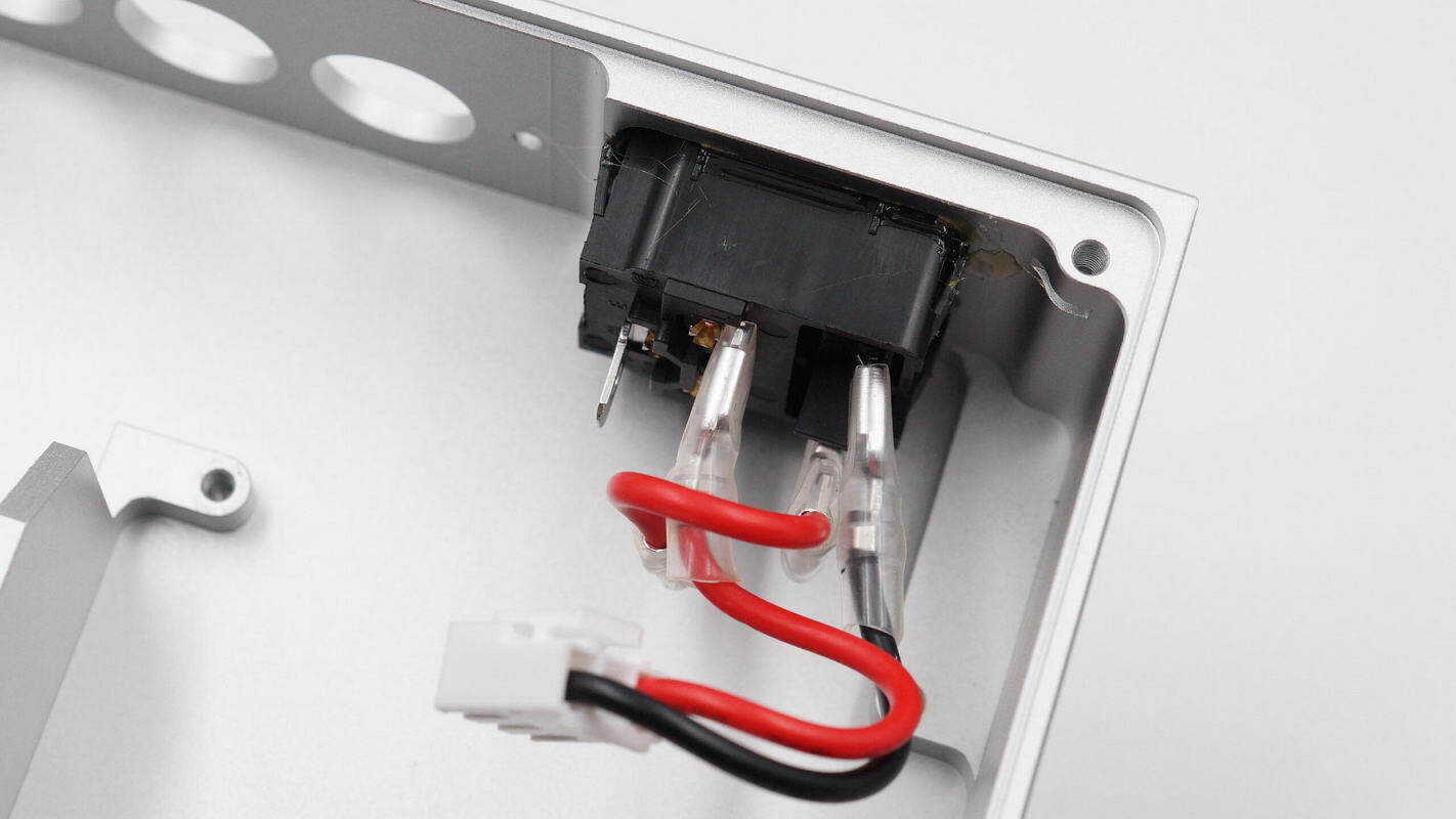
On the rear panel, there are line-level input jacks, an XLR input, amplifier output binding posts, and a power input connector.
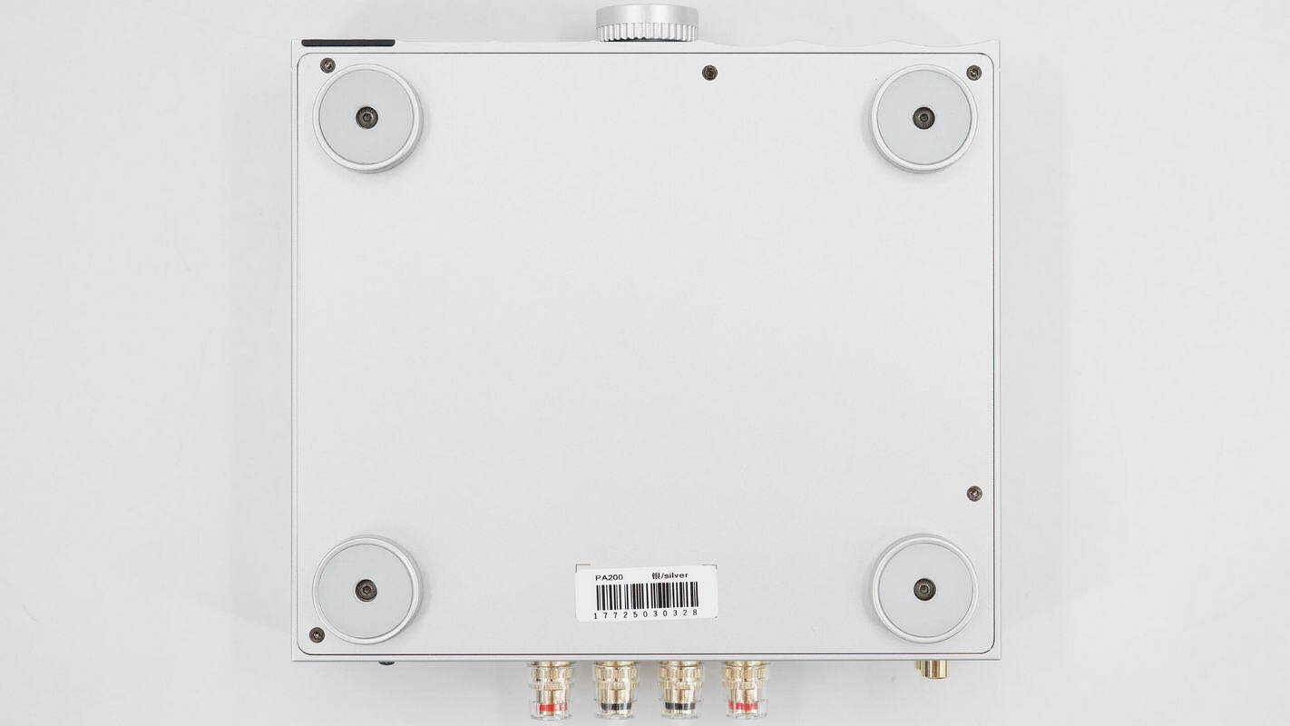
On the bottom side, a cover plate is secured in place with screws.
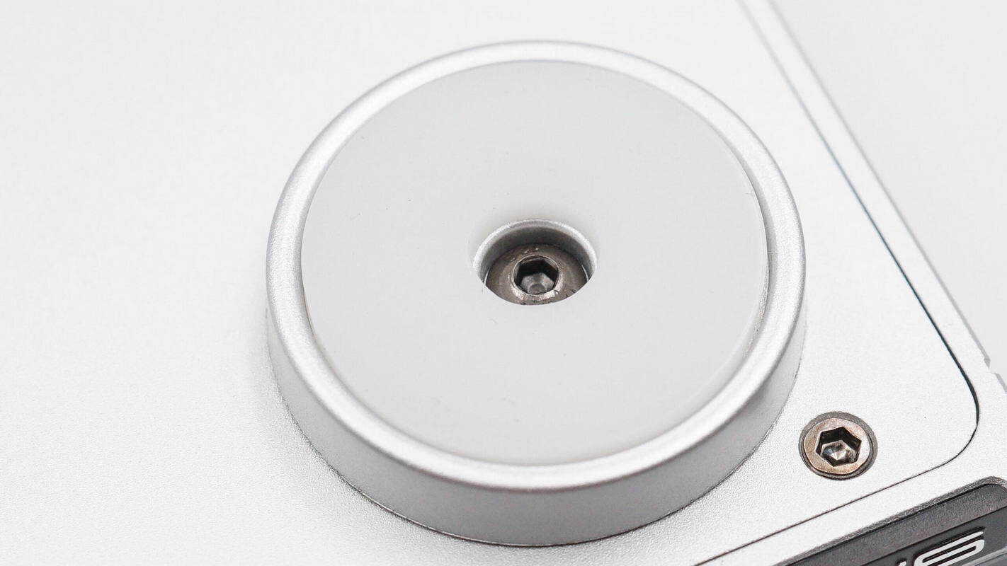
The bottom side is fitted with rubber feet.
Teardown
Next, let's take it apart to see its internal components and structure.
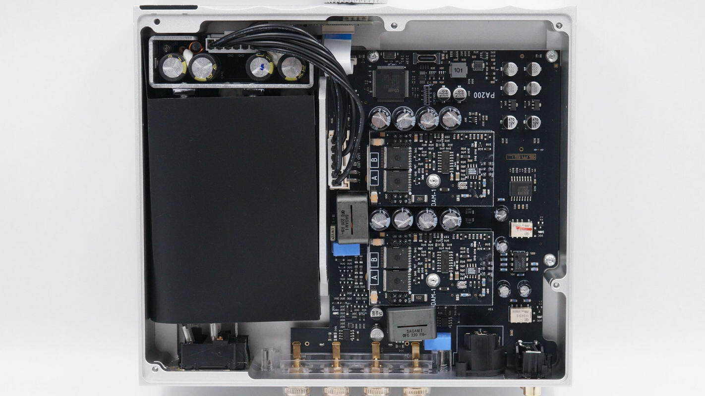
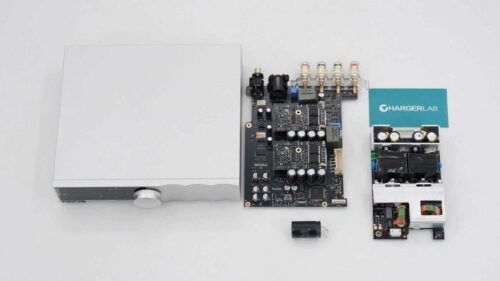
After removing the screws and taking off the bottom cover plate, the interior is revealed to be divided into two sections: the switching power supply module and the amplifier module.
The enclosure is CNC-machined, and an internal partition separates the two modules.
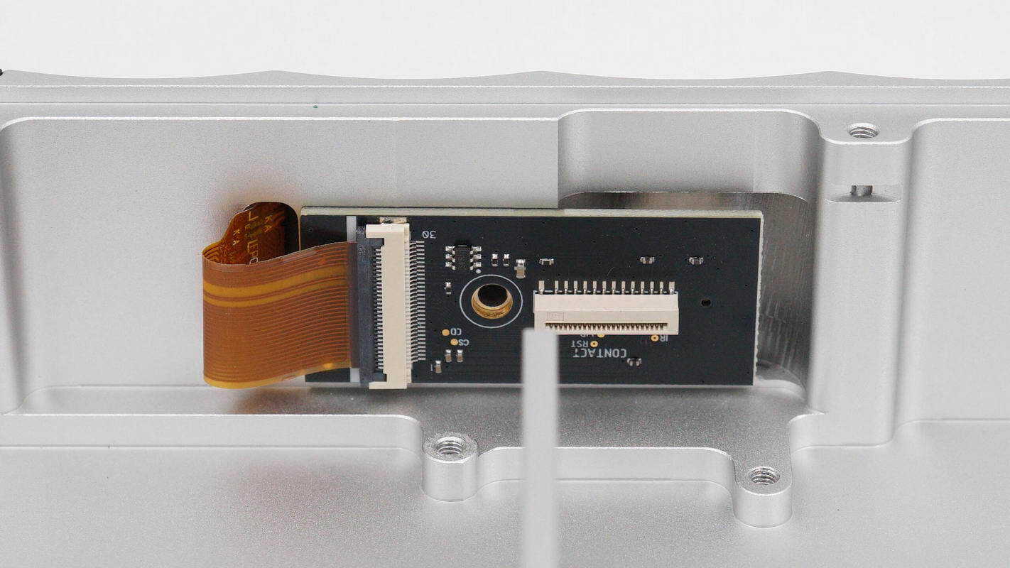
The display PCB is connected via a ribbon cable.
The connector is secured with adhesive.

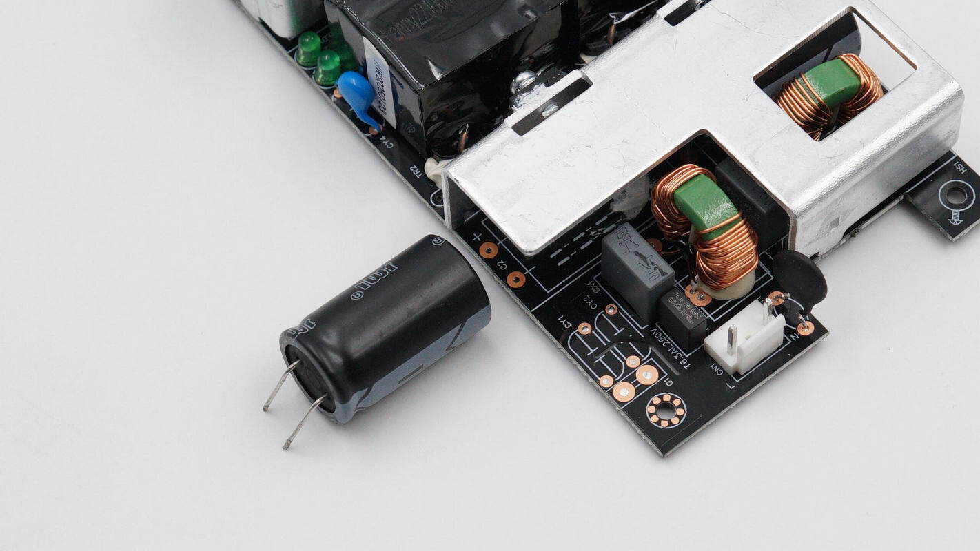
The switching power supply module features mica insulation.
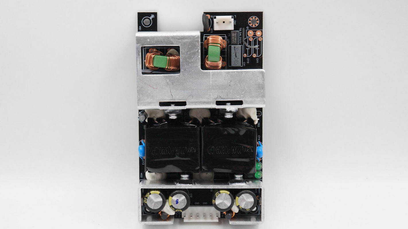
The front side of the switching power supply module includes a fuse, safety X2 capacitor, common mode choke, primary MOSFETs, bridge rectifier, high-voltage filter capacitors, transformers, and rectifiers.
The rear side features a master control chip, a feedback optocoupler, and other components.
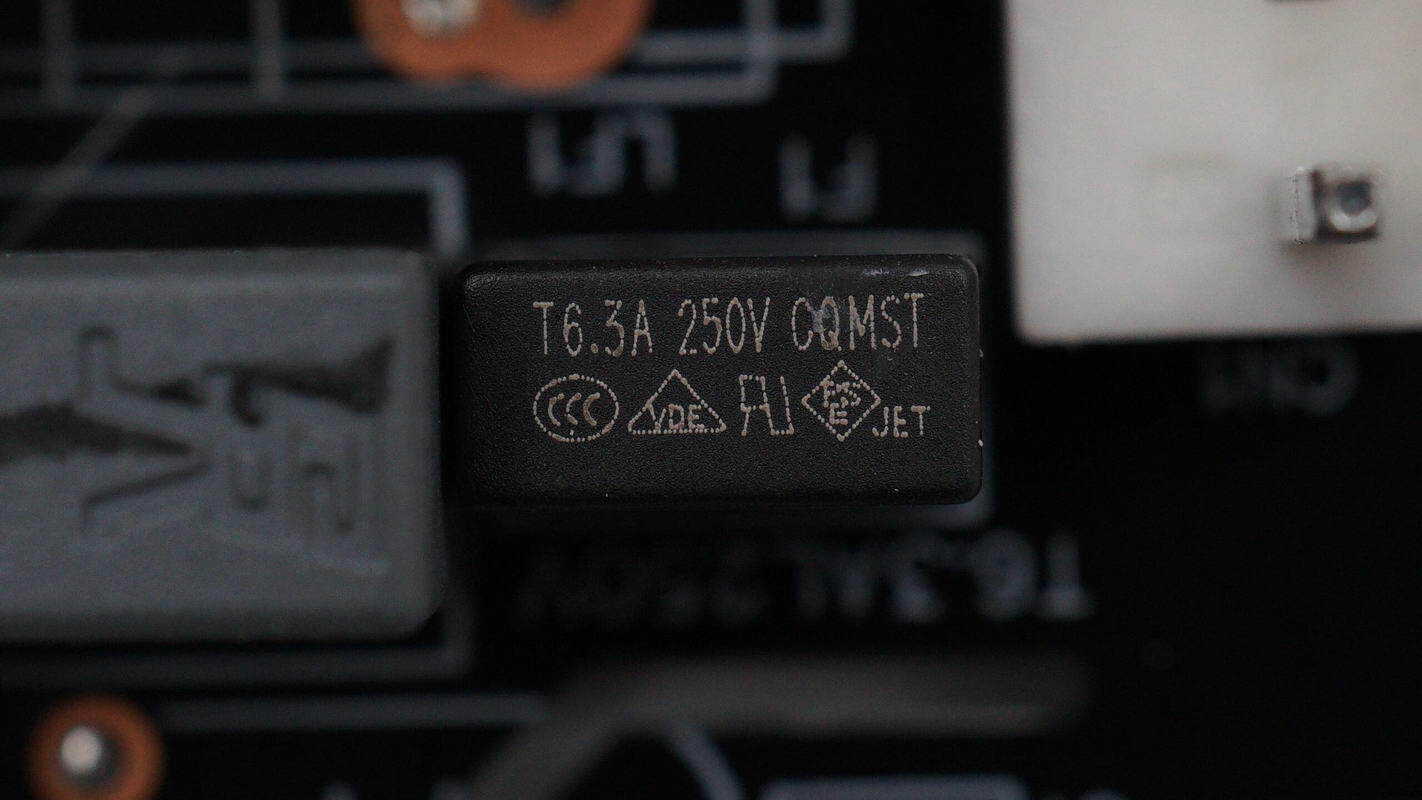
The input fuse is from CONQUER, with a rating of 6.3 A, 250 V.
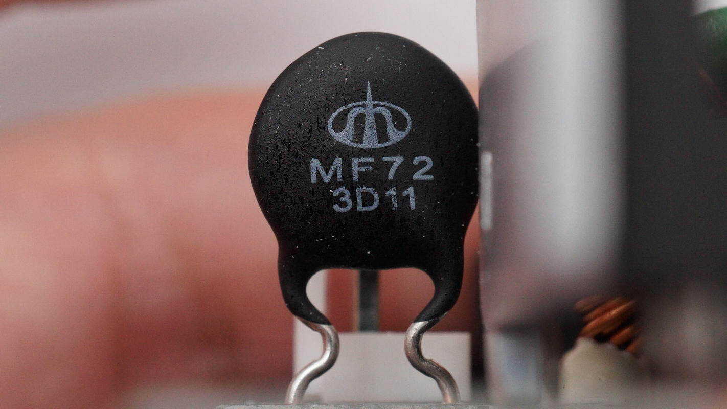
The NTC thermistor is from Shiheng, MF72 series, marked 3D11, and is used to suppress inrush current during power-up.
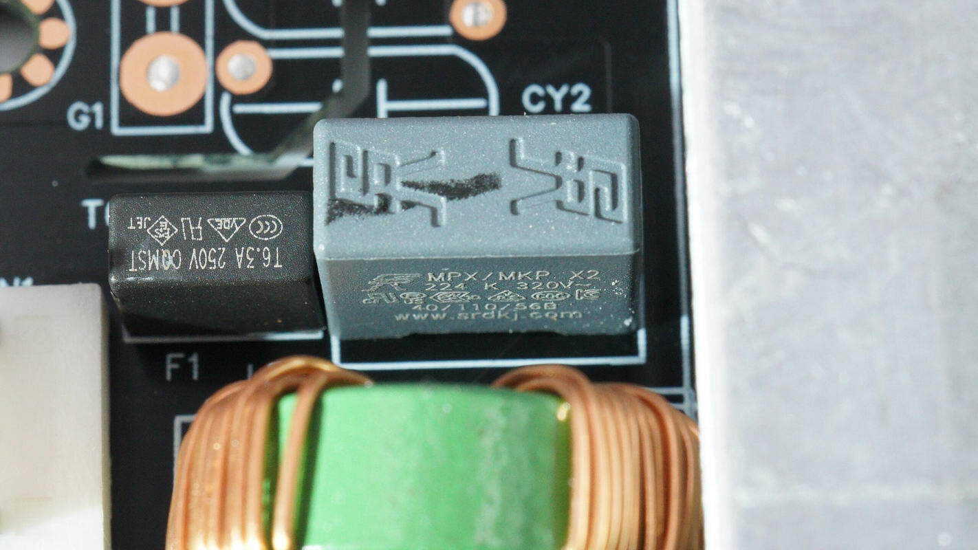
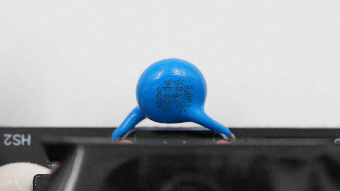
The safety X2 capacitor is from SINCERITY, with a capacitance of 0.22 μF.
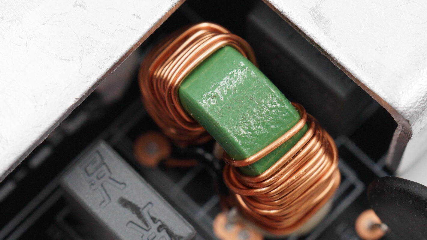
The common mode choke is wound with enameled wire.
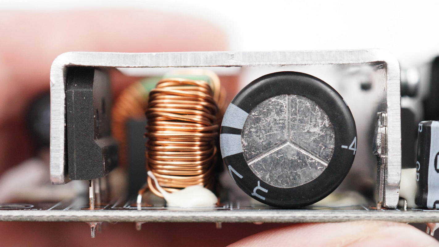
Beneath the heatsink are the bridge rectifier, common mode choke, and a high-voltage filter capacitor.
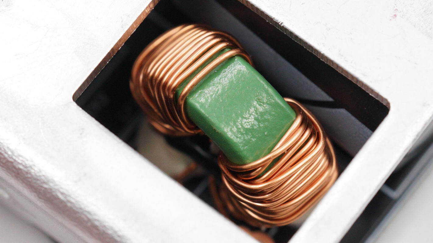
Another common mode choke is also wound with enameled wire.
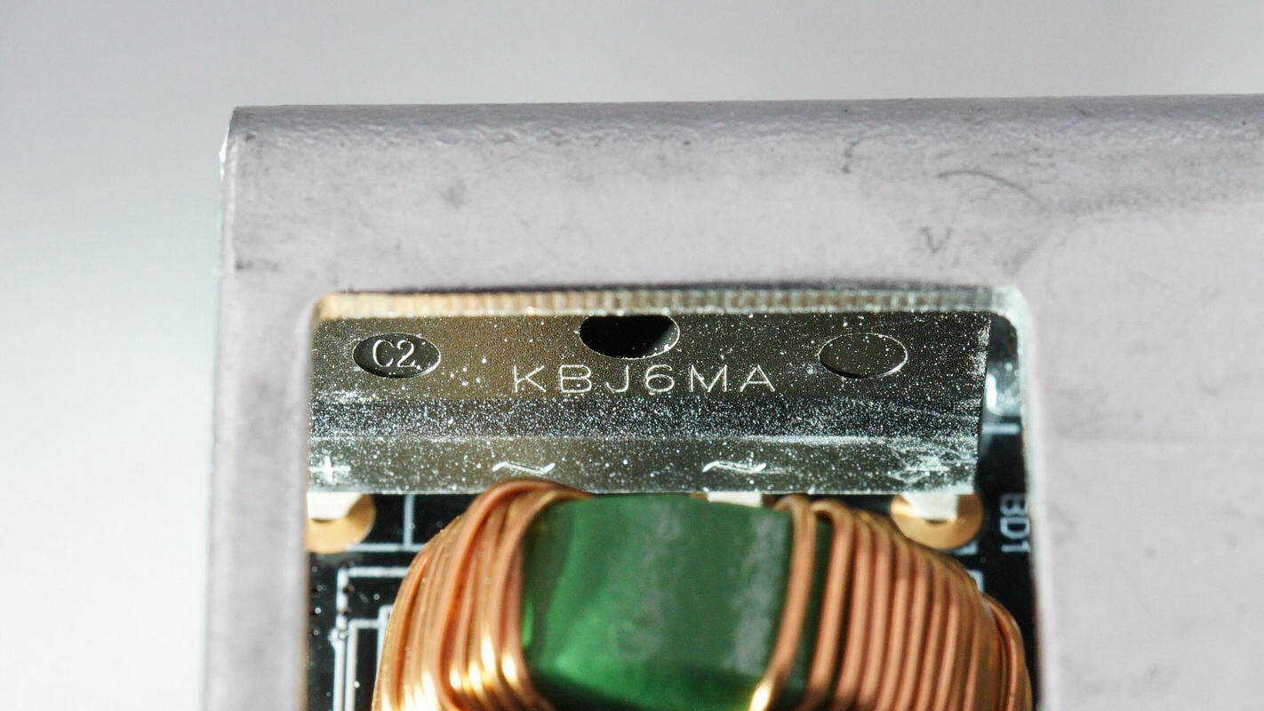
The bridge rectifier is model KBJ6MA, rated 6A 1000V, and comes in a KBJ package.
Remove the high-voltage filter capacitor.
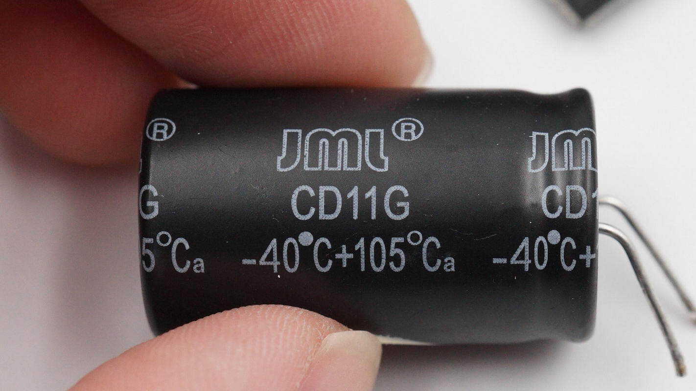
The capacitor is from JML.
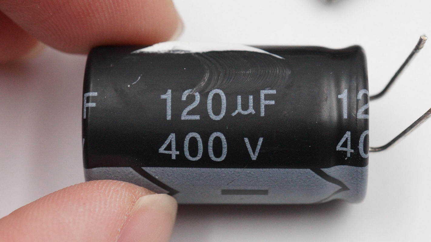
It is rated at 120 μF, 400 V.
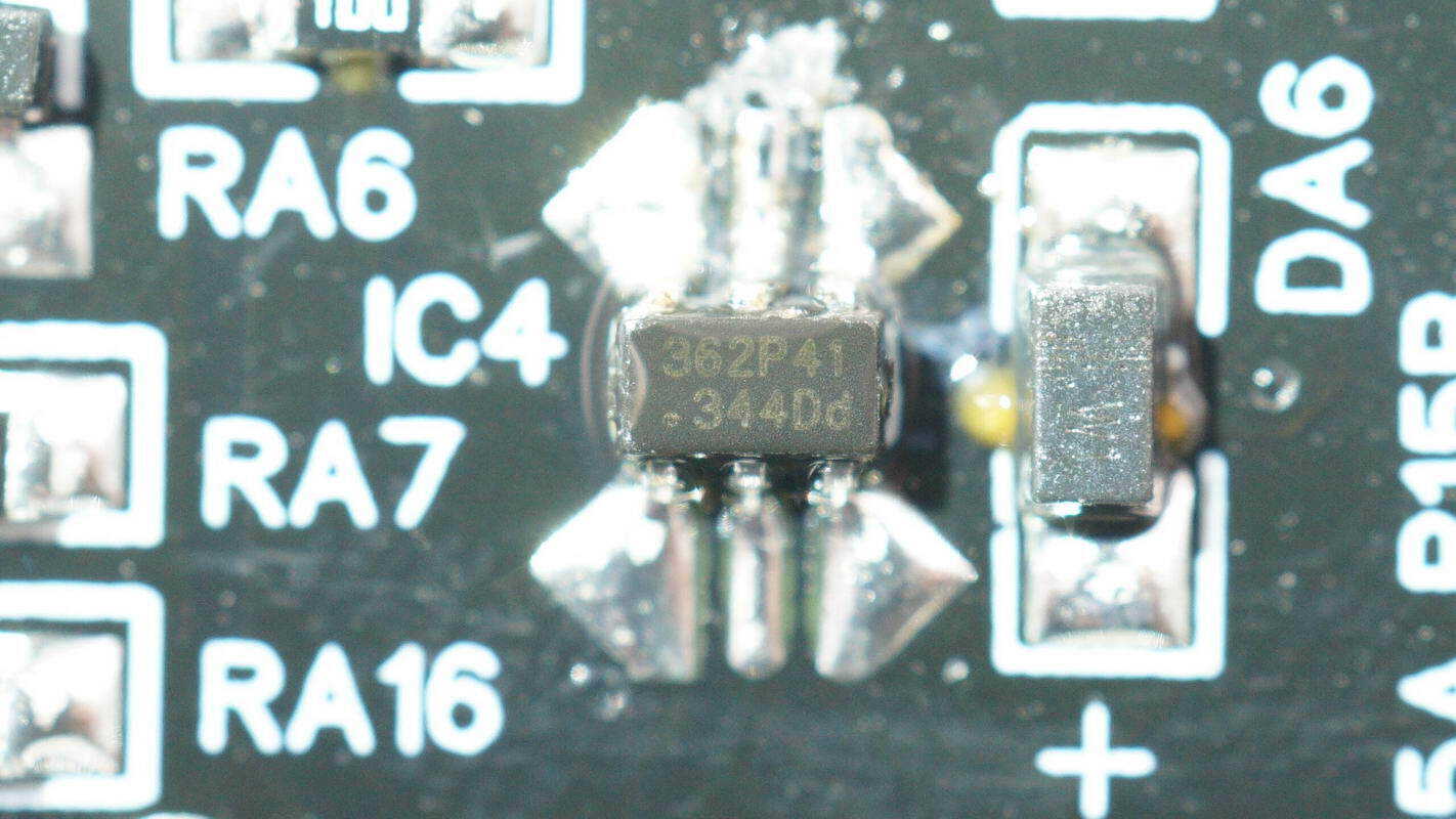
The master control chip is from On-Bright, model OB2362D. It is a high-performance flyback switching power supply controller that supports multiple operating modes and comprehensive protection features. It comes in a SOT23-6 package and is suitable for power adapter applications.
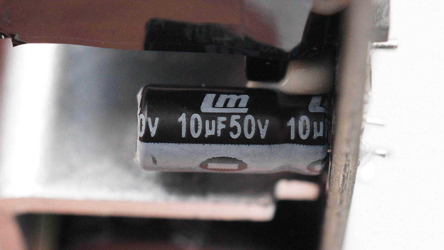
The filter capacitor supplying power to the master control chip is rated at 10 μF, 50 V.
The primary MOSFETs are mounted on the heatsink.
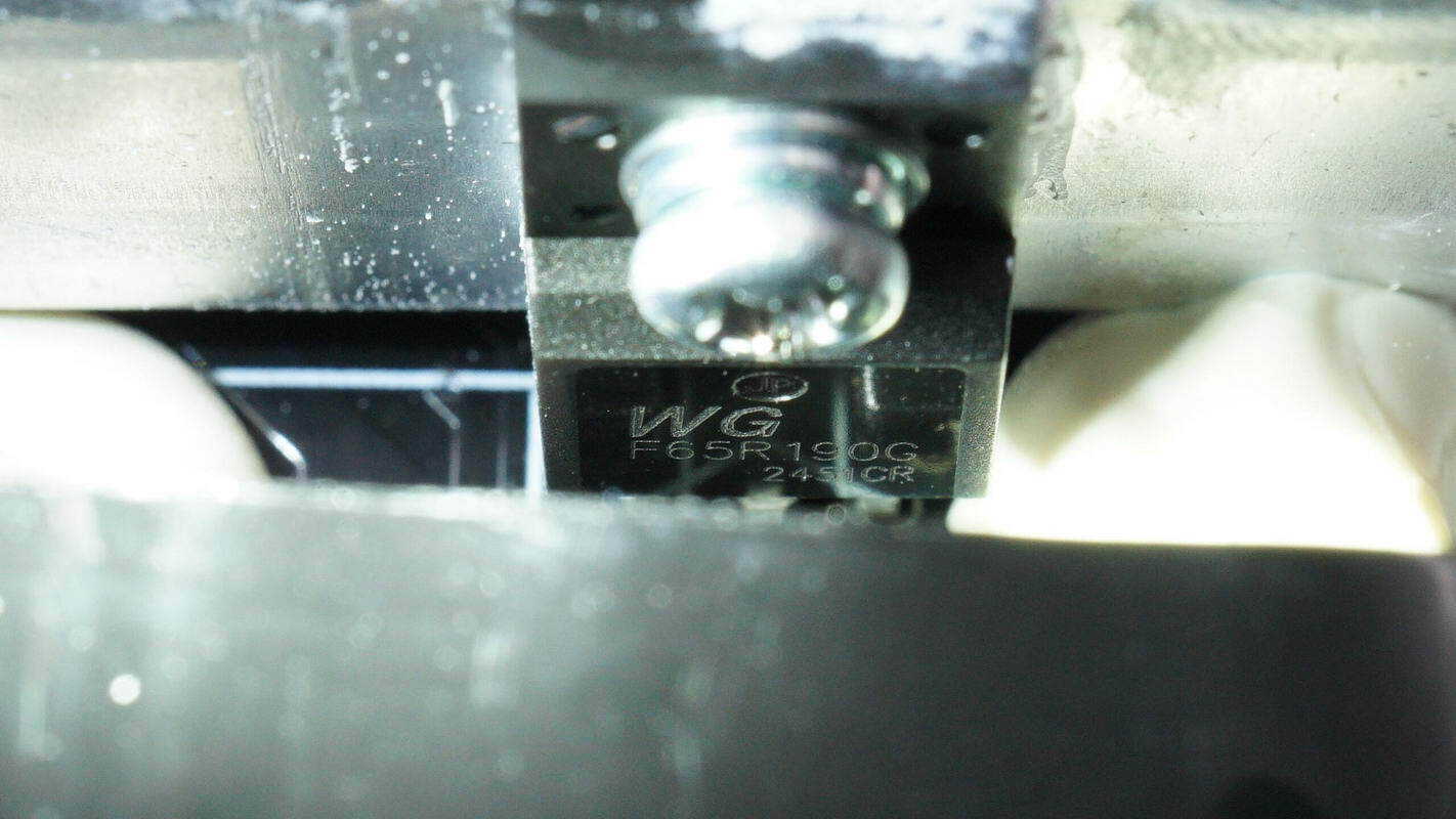
The primary MOSFETs are from WGSEMİ, model WGF65R190G. They are NMOS devices with a voltage rating of 650V, an on-resistance of 165mΩ, and come in a TO-220F package.
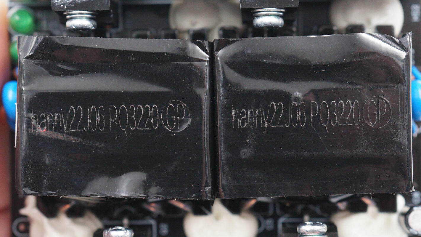
The transformers use PQ3220 cores and are insulated with winding tape.
The blue Y capacitor is from Howa.
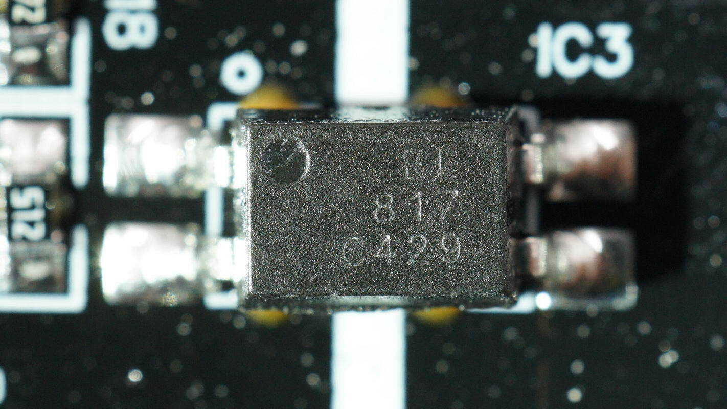
The Everlight EL817 feedback optocoupler is used for output voltage feedback.
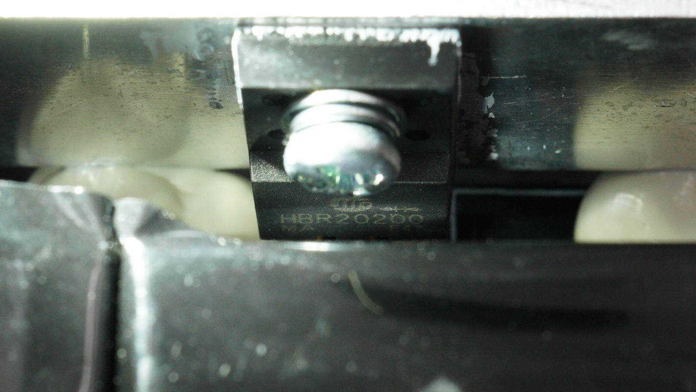
The rectifier is from HWDZ, model HBR20200. It is a Schottky diode rated at 20 A, 200 V, and comes in a TO-220HF package.

The output stage is equipped with filter capacitors and a filter inductor.

The filter capacitors are sourced from Chengx.
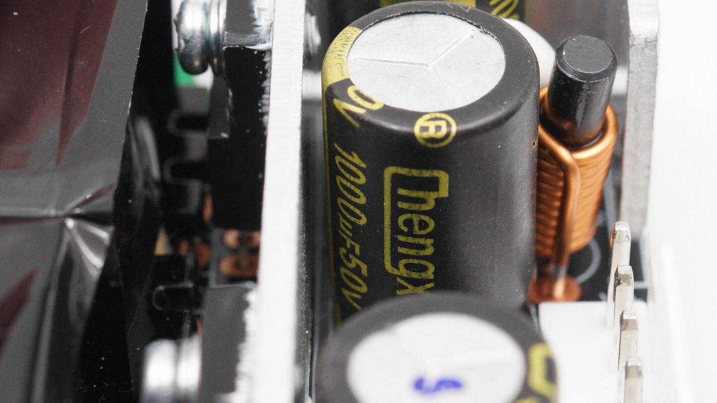
They are rated at 1000 μF, 50 V, with a total of two units.
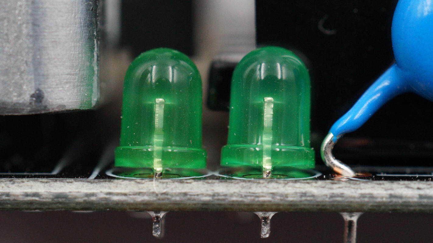
Two green LEDs are used for power indication.
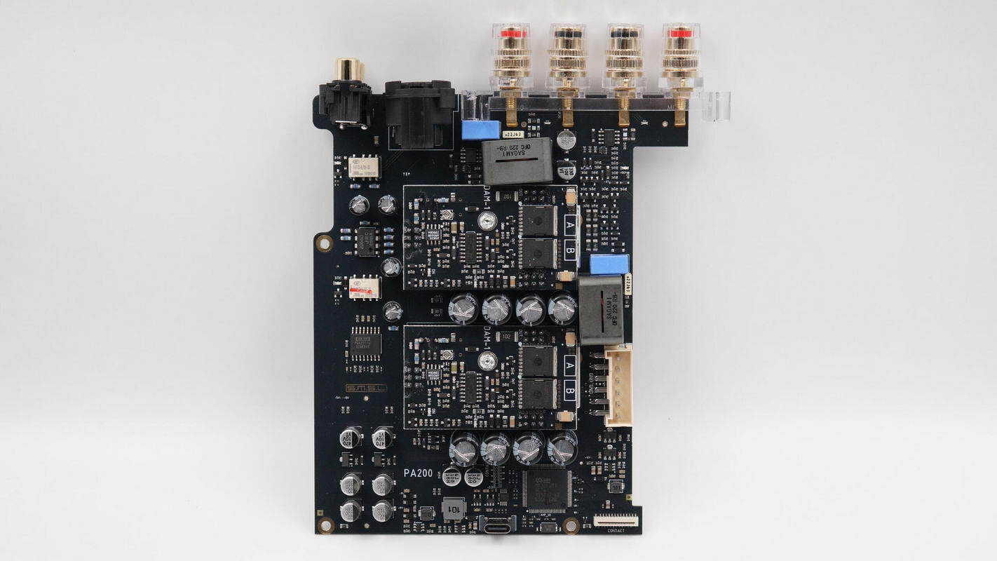
The front side of the amplifier module features relays, a digital potentiometer, regulator chips, filter capacitors, an MCU, and other components.
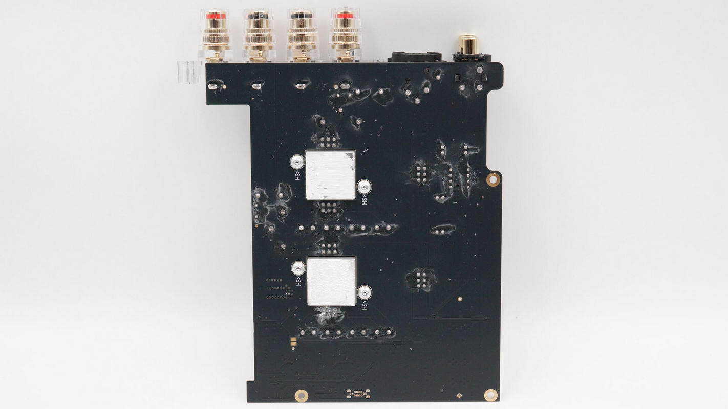
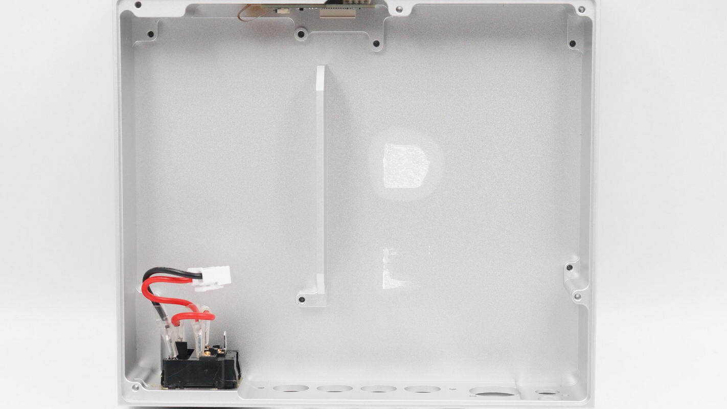
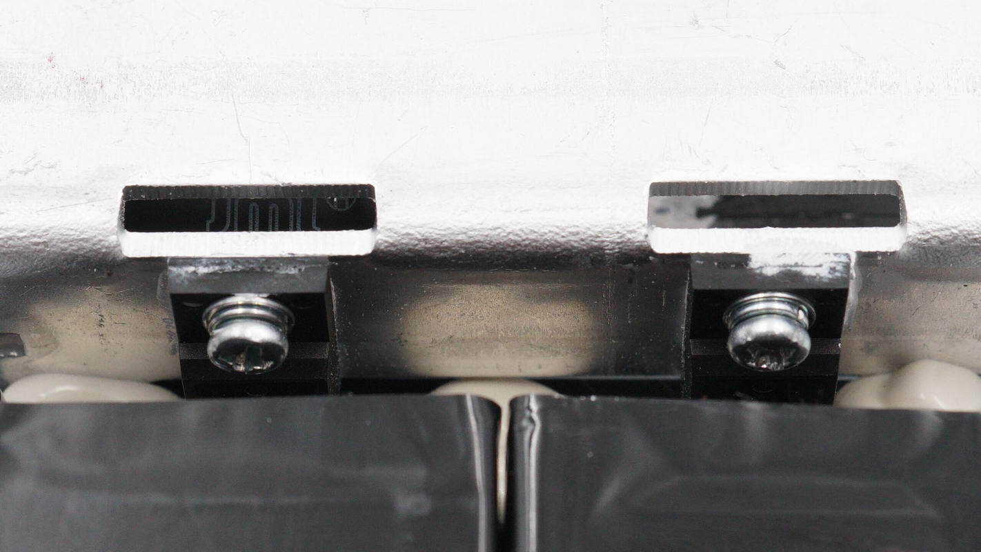
The rear side has two aluminum blocks, secured with screws.
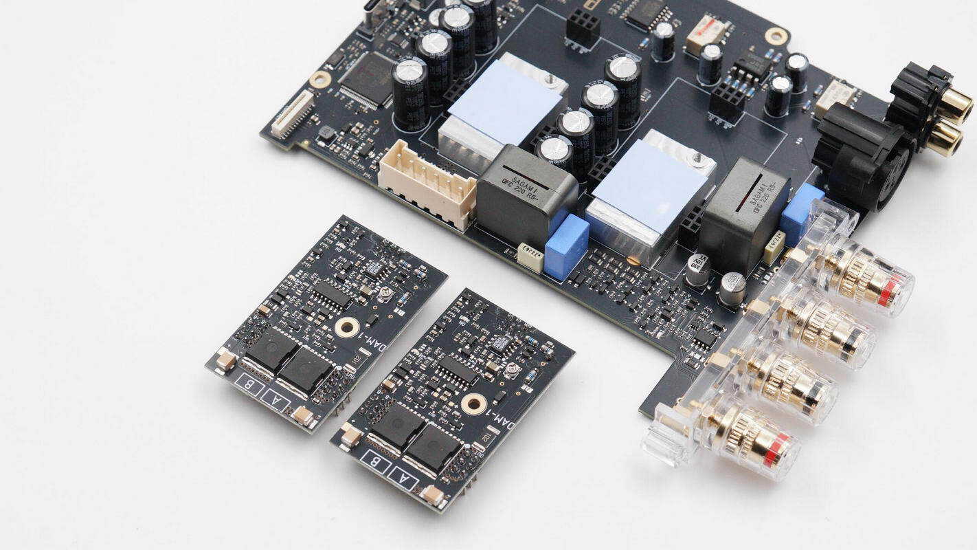
Remove the two small PCBs.
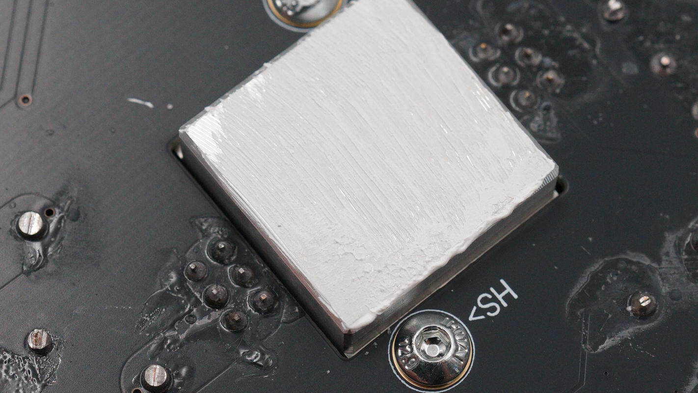
The aluminum block is coated with thermal grease and thermally connected to the chassis.
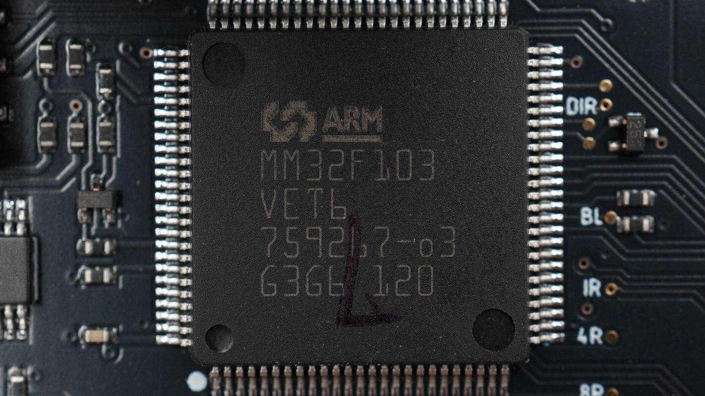
The MCU is from MindMotion, model MM32F103VET6. It features an ARM Cortex-M3 core running at 96 MHz, with 512 KB of flash memory and 128 KB of SRAM. It supports a 2.0–5.5 V operating voltage and provides 8 UART interfaces, 2 I²C interfaces, 3 SPI interfaces, 1 CAN interface, 1 USB OTG interface, and 1 SDIO interface. The device comes in an LQFP100 package.
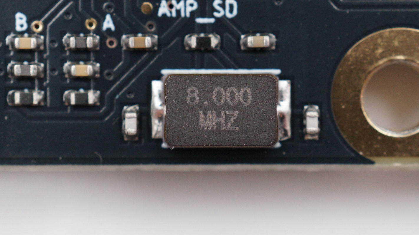
Close-up of the external 8.000 MHz crystal oscillator connected to the MCU.
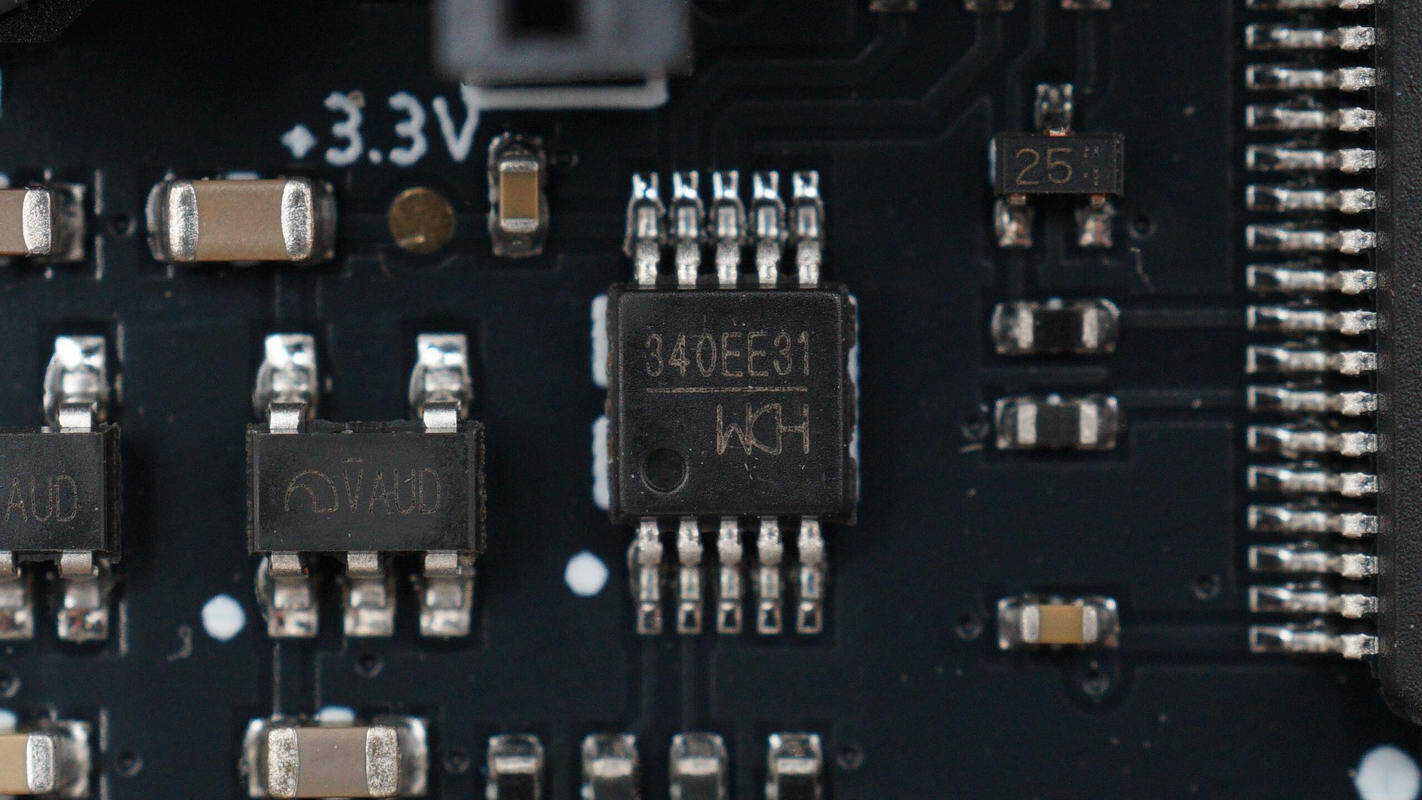
The serial interface converter chip is from WCH, model CH340E. It is used for USB-to-serial or USB-to-printer conversion, features a full-speed USB device interface, is compatible with USB 2.0, supports 5V and 3.3V power supply, and comes in an MSOP10 package.
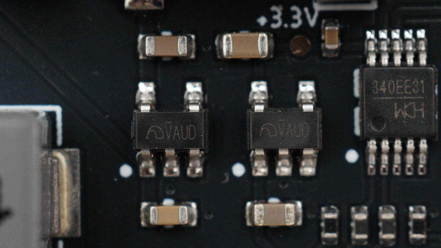
The regulator chips are from Microne, marked VAUD, and come in SOT23 packages.
The USB-C socket is secured through via-hole soldering.
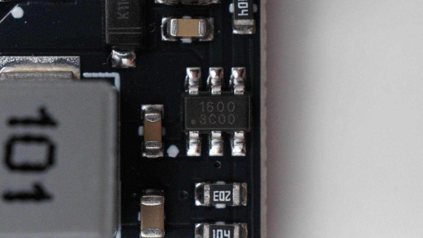
The buck converter chip is from GOSEMICON, model GBI1600. It is a non-synchronous step-down converter with an input voltage range of 4–60 V, featuring a built-in MOSFET, 1 A output current capability, and a 600 kHz switching frequency. It includes undervoltage protection, over-temperature protection, and cycle-by-cycle current protection, and comes in a TSOT23-6L package.
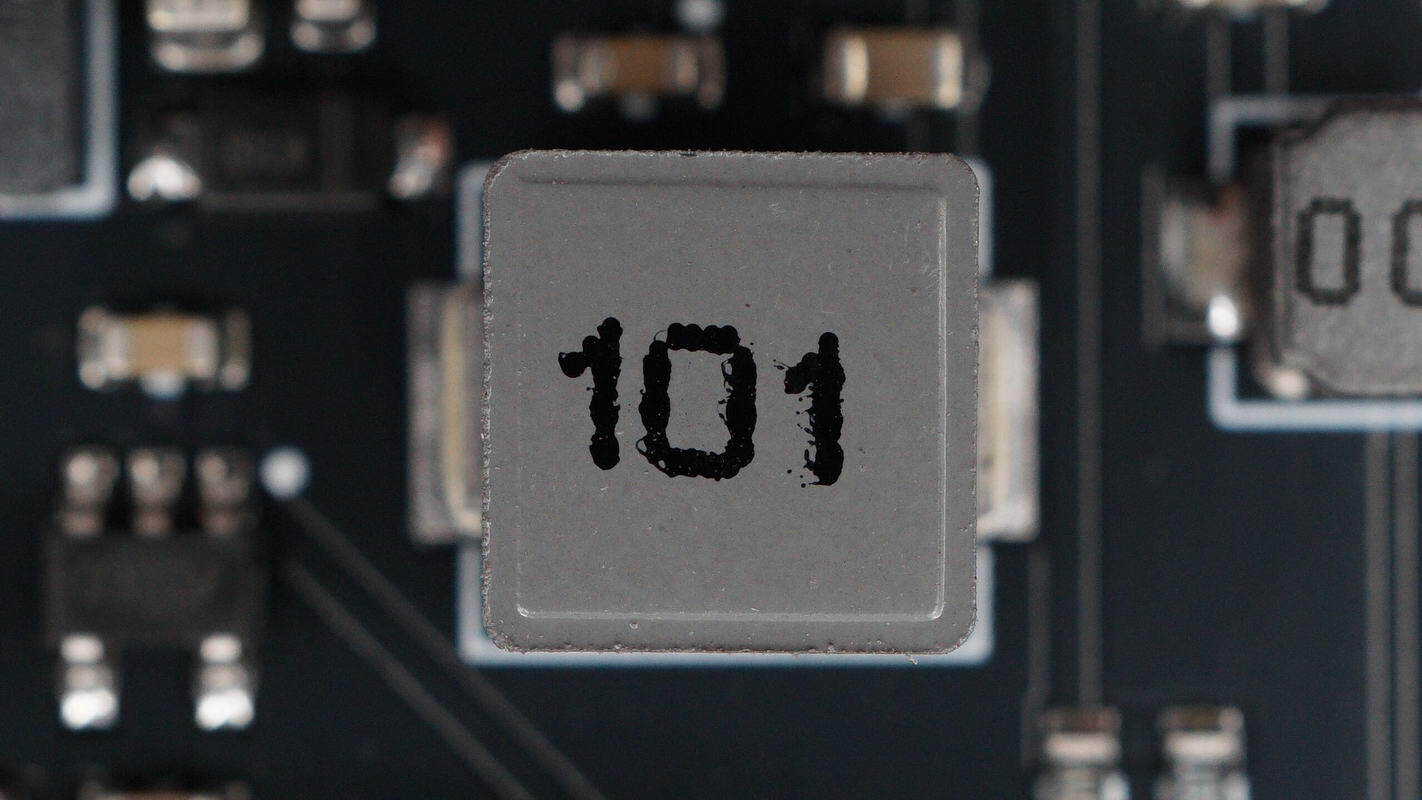
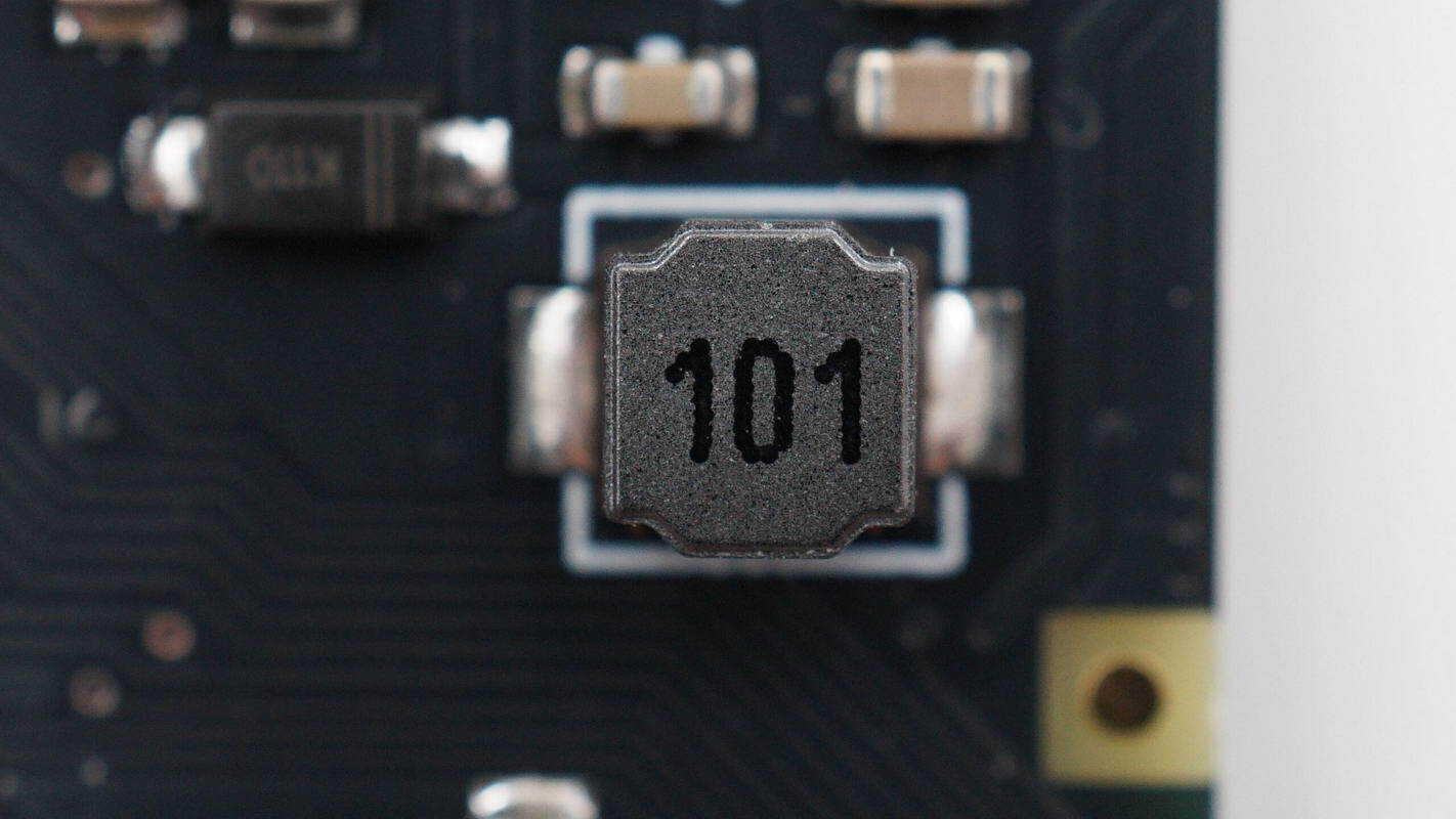
Close-up of the 100μH buck inductor.
The filter capacitors are all rated at 100 μF, 16 V.

The other buck converter chip is also a GOSEMICON GBI1600.
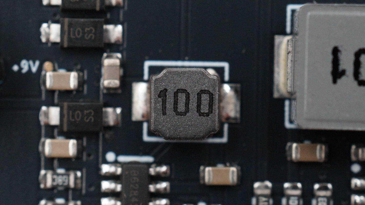
Close-up of another 100 μH buck inductor.
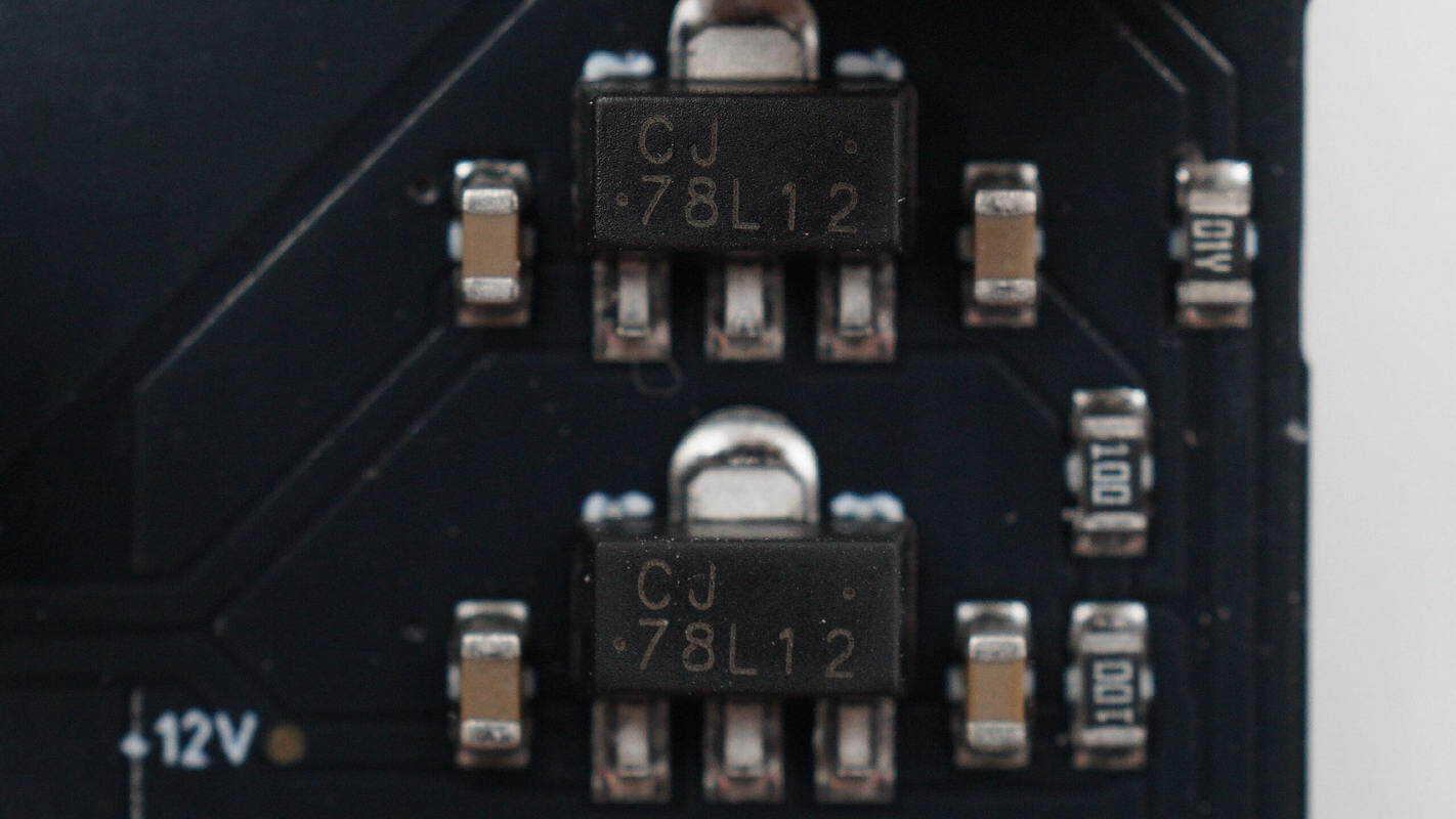
The two regulator chips are from JSCJ, model CJ78L12. They support an input voltage of 35 V, an output of 12 V at 100 mA, and come in an SOT-89-3L package.
The two regulator chips are from JSCJ, model CJ78L12. They support an input voltage of 35V, an output of 12V at 100mA, and come in an SOT-89-3L package.
Close-up of the 10μH boost inductor.
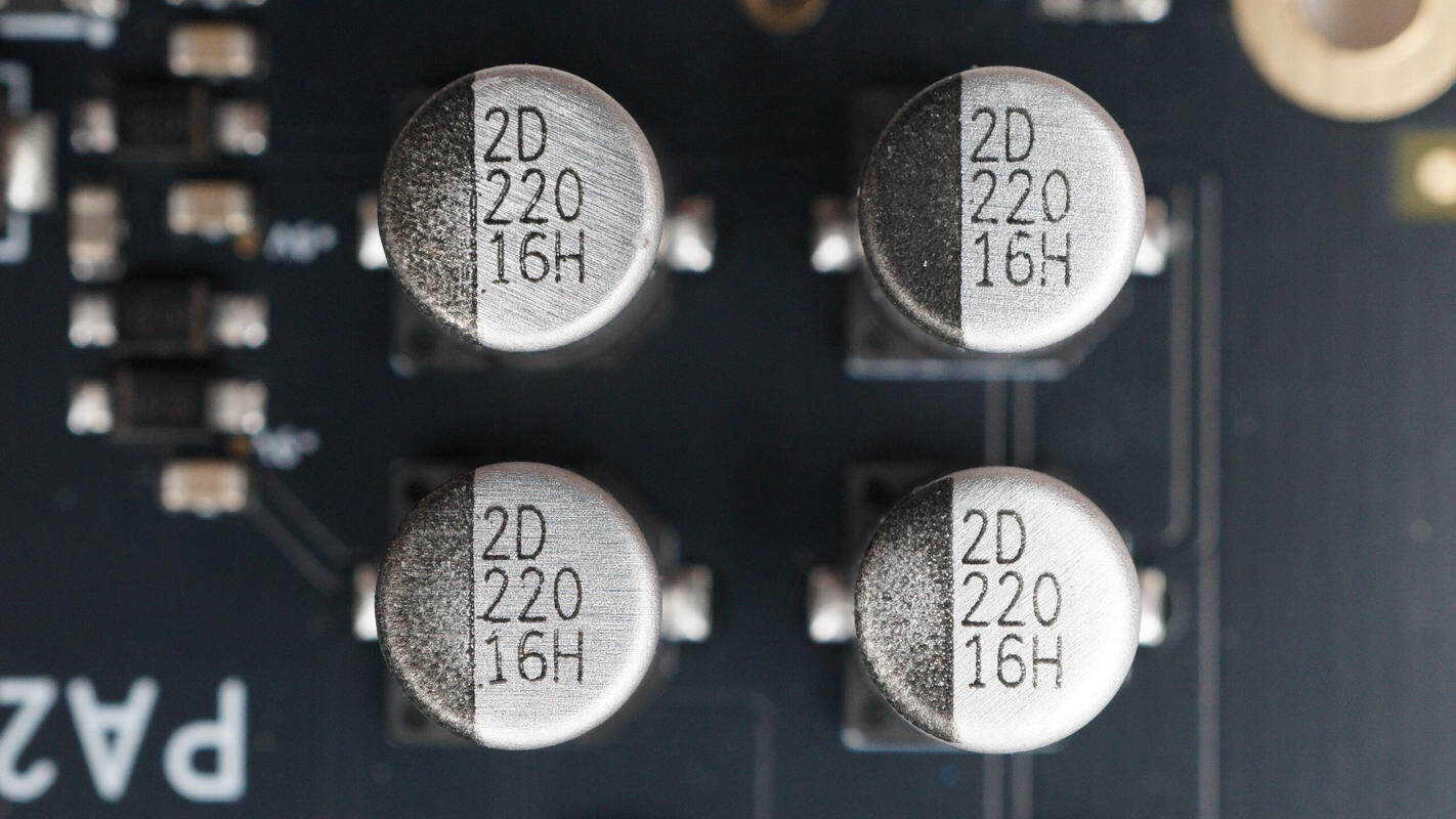
The filter capacitors are rated at 220 μF, 16 V.
The two regulator chips have their model markings removed.
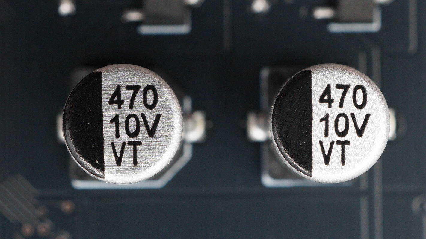
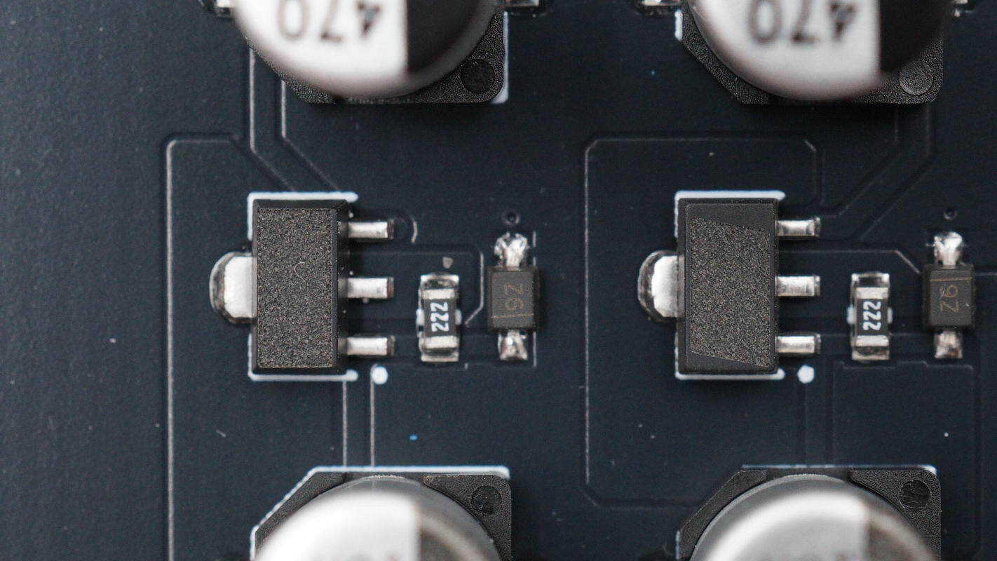
The filter capacitors are rated at 470 μF, 10 V.
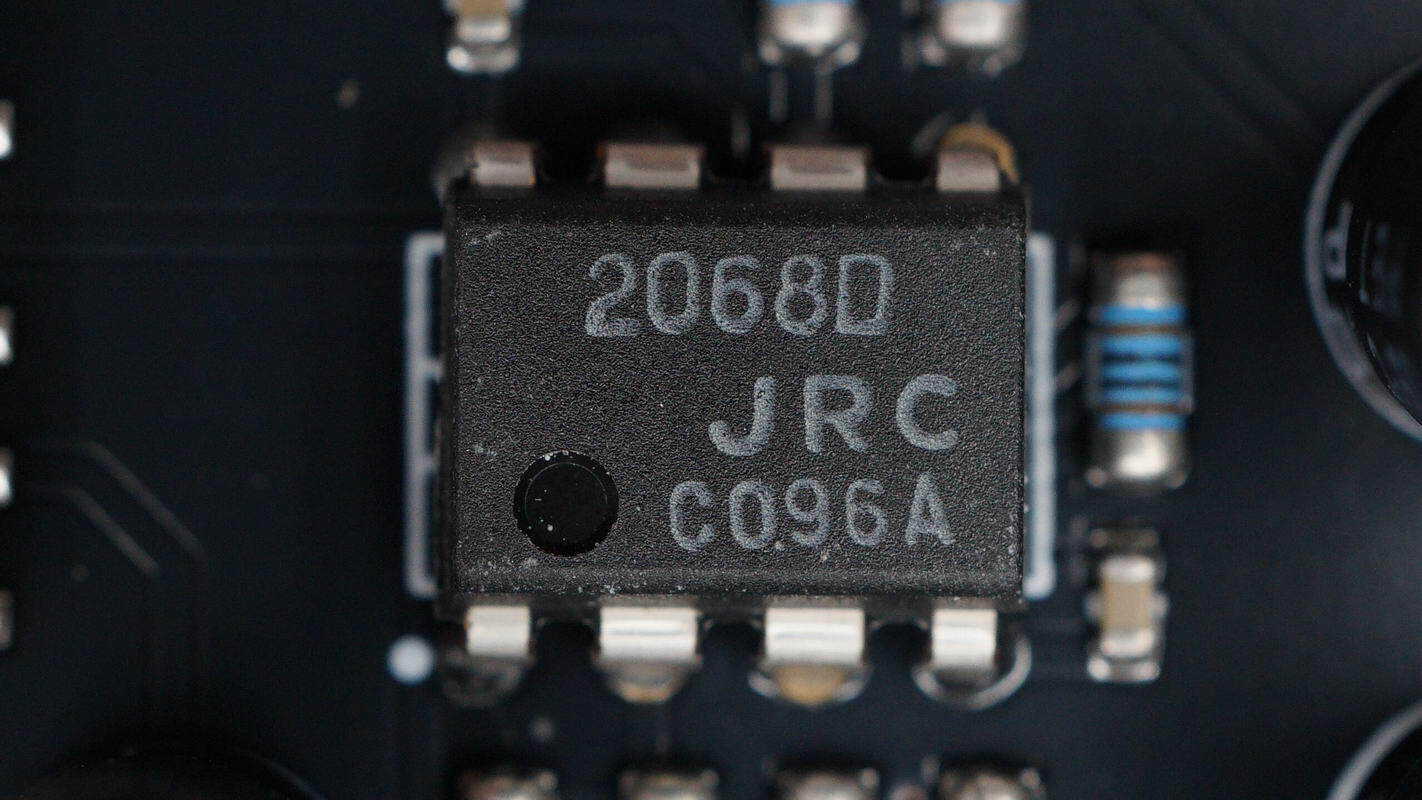
The operational amplifier is from NISSHINBO, model NJM2068D. It is a low-noise dual op-amp, supporting a ±4 V to ±18 V operating voltage, and comes in a DIP8 package.
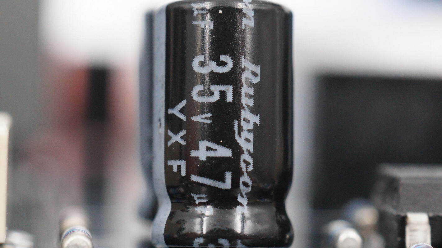
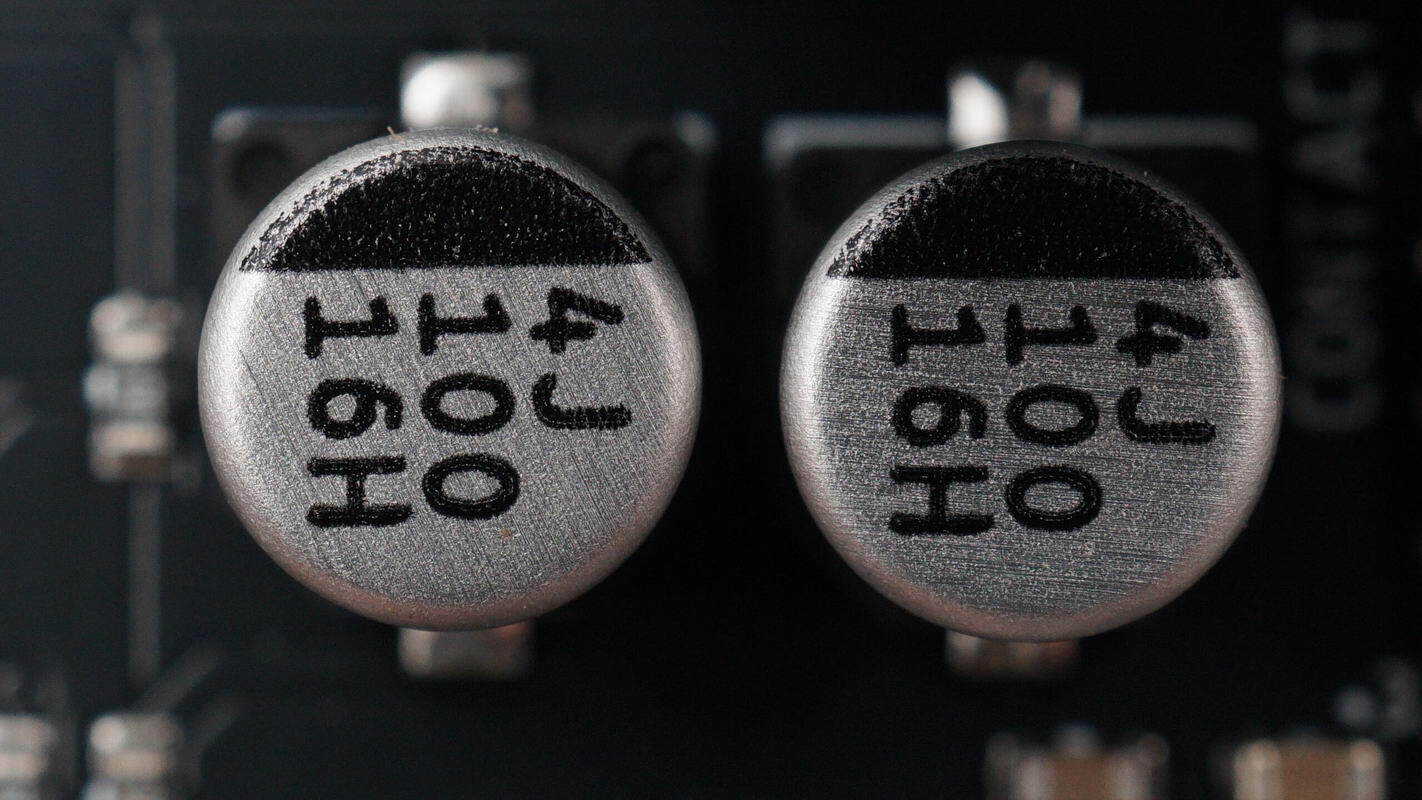
The electrolytic capacitors are from Rubycon, rated 47 μF, 35 V, with a total of four units.
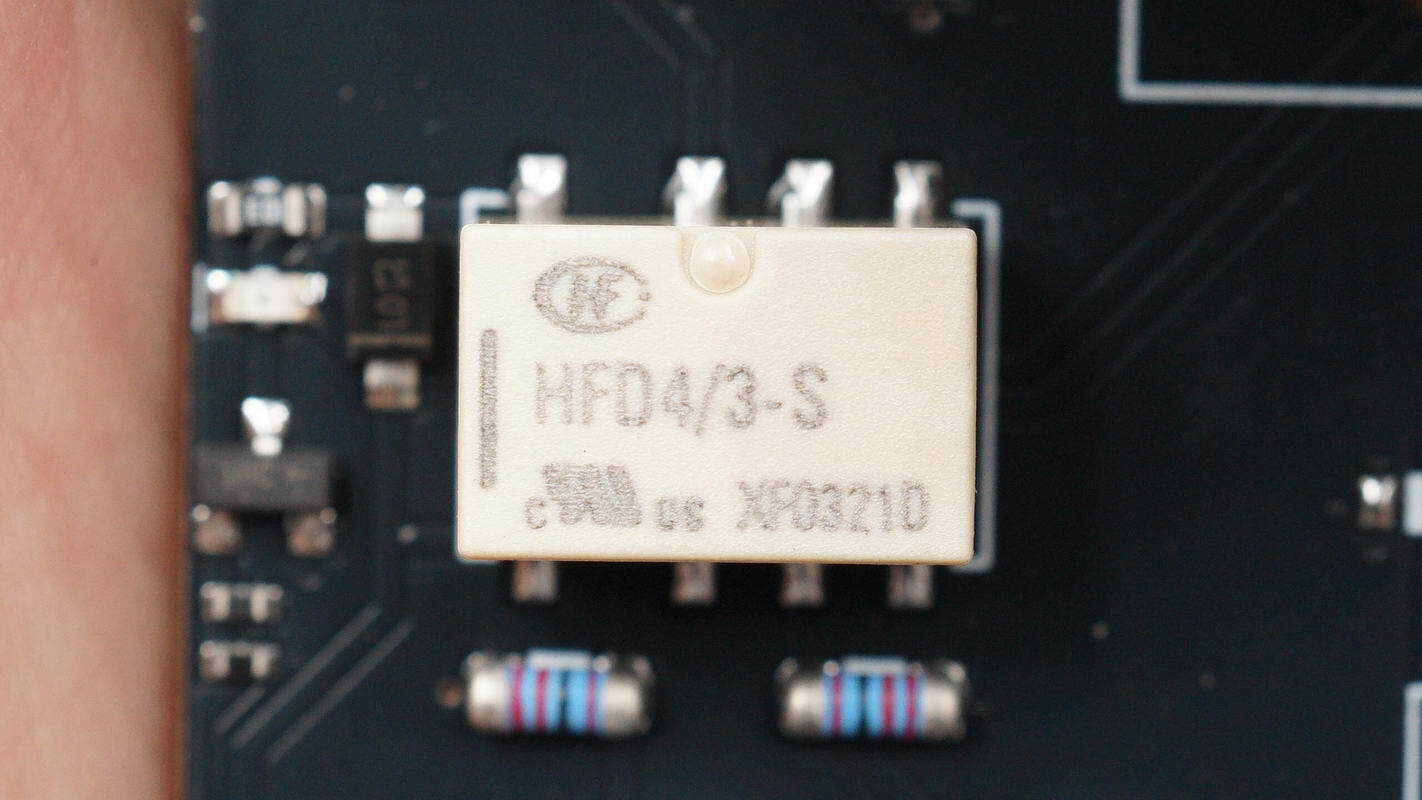
The switching relay is from HONGFA, model HFD4/3‑S. It is an ultra-compact fourth-generation signal relay with a contact rating of 2 A, 30 V DC, and comes in a standard surface-mount package.

The other relay has the same model.
The digital potentiometer is from TI, model PGA2311. It is a high-performance stereo volume control chip featuring internal high-performance operational amplifiers, capable of directly driving a 660 Ω load. It provides a three-wire serial control interface and comes in an SOIC-16 package.
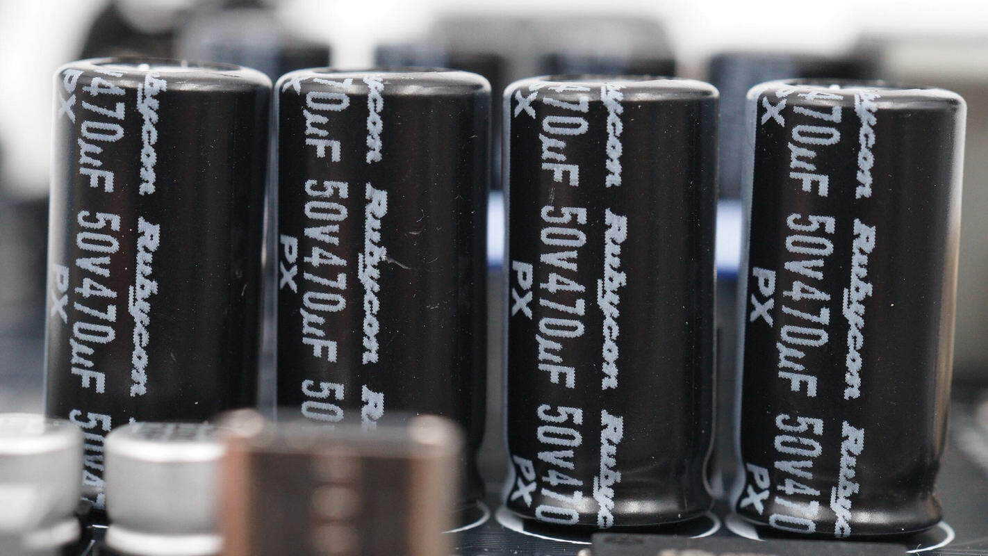
The filter capacitors are from Rubycon, each rated at 470 μF, 50 V, with a total of eight units used.
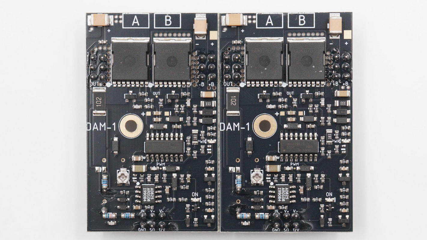
The front side of the GaN amplifier module features operational amplifiers, drivers, and GaN FETs.

The rear side is soldered with header pins and equipped with an electrolytic capacitor.
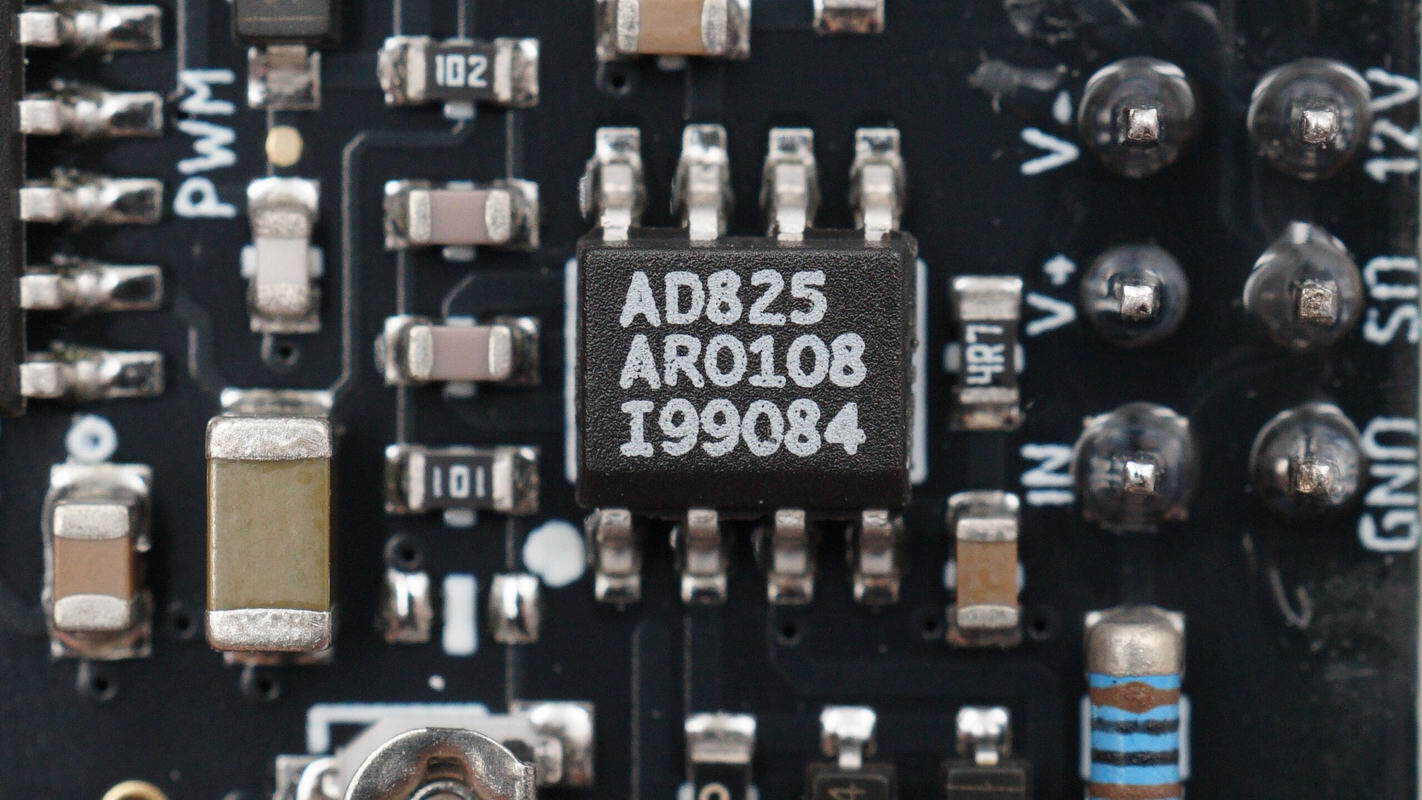
The operational amplifier is from ADI, model AD825. It is a general-purpose high-speed JFET amplifier, supporting a ±5 V to ±15 V supply voltage, with a slew rate of 125 V/μs and high output drive capability. It comes in an SOIC-8 package.
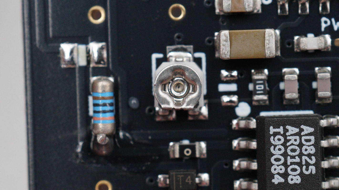
Close-up of the trimmer potentiometer.
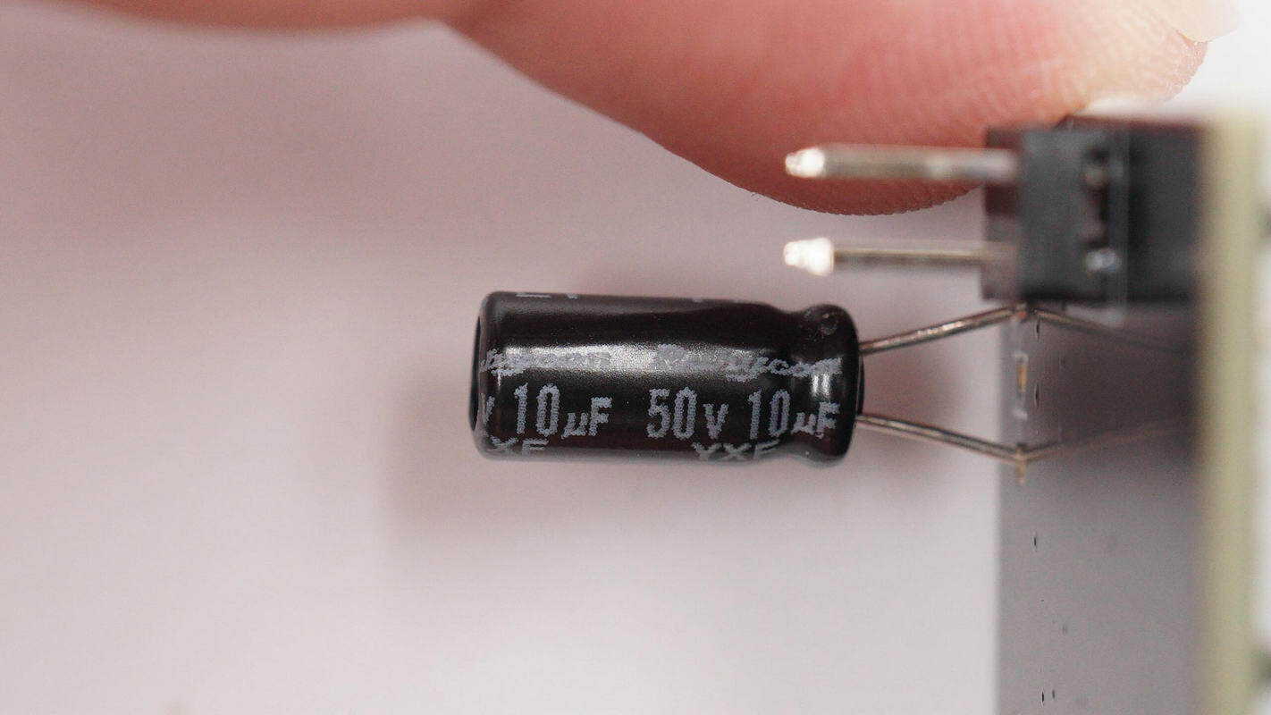
The filter capacitor is rated at 10 μF, 50 V.
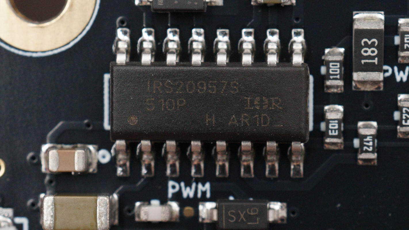
The driver is from Infineon, model IRS20957S. It is a high-voltage, high-speed MOSFET driver featuring floating PWM inputs, a switching frequency of up to 800 kHz, and support for ±100 V supply voltage. It offers high noise immunity, dual overcurrent and shoot-through protection, as well as undervoltage lockout for the bias supply, and comes in an SOIC-16 package.
The MLCC capacitor is used for power supply filtering.
The driver is from Infineon, model IRS20957S. It is a high-voltage, high-speed MOSFET driver featuring floating PWM inputs, a switching frequency of up to 800 kHz, and support for ±100 V supply voltage. It offers high noise immunity, dual overcurrent and shoot-through protection, as well as undervoltage lockout for the bias supply, and comes in an SOIC-16 package.
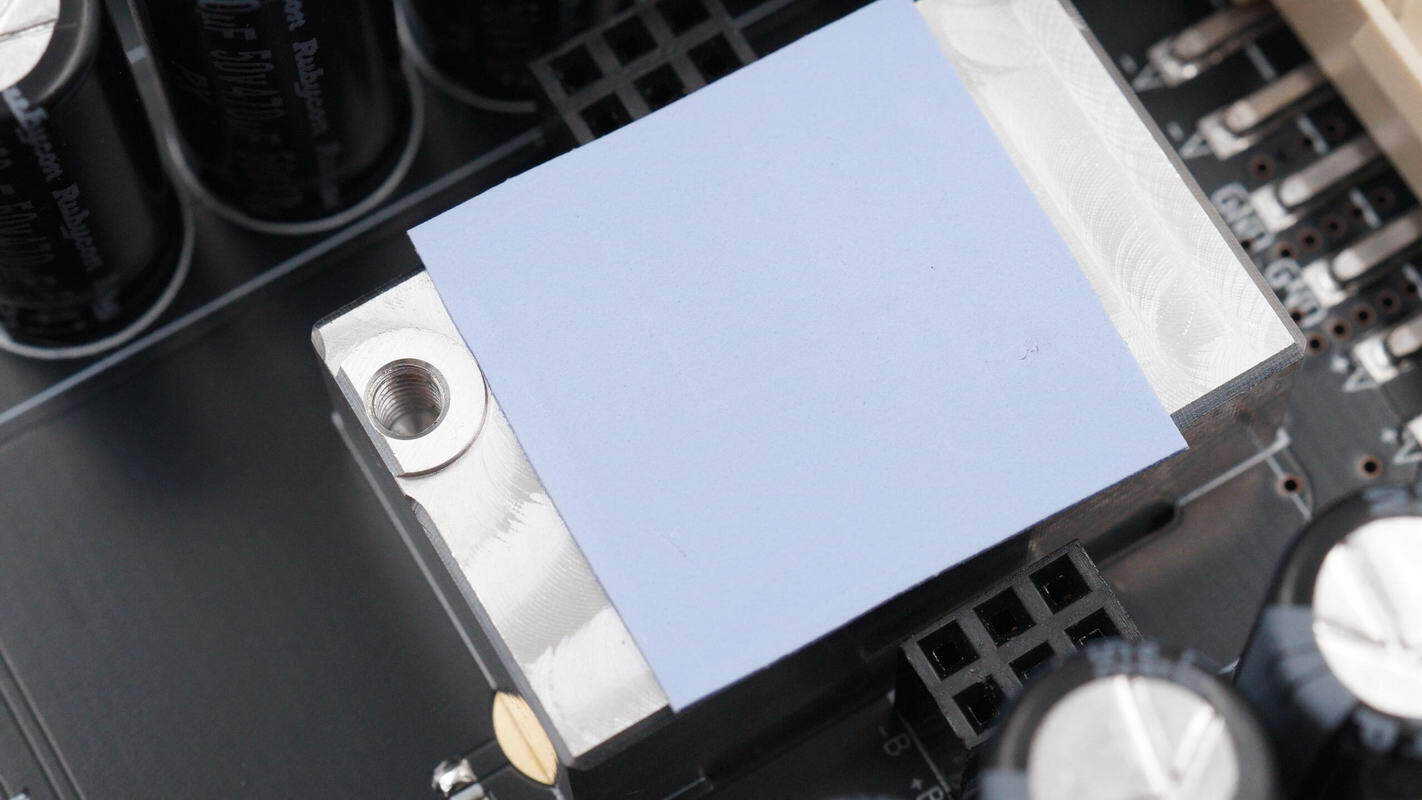
Beneath the GaN amplifier module, a thermal pad and heatsink block are installed and secured with screws.
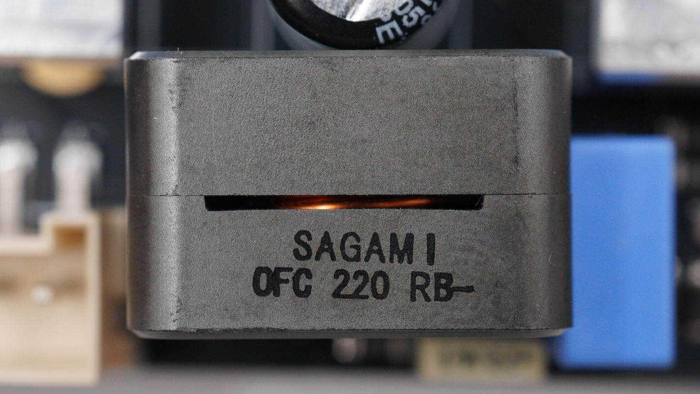
The filter inductor is wound with oxygen-free copper wire and is rated at 22 μH.
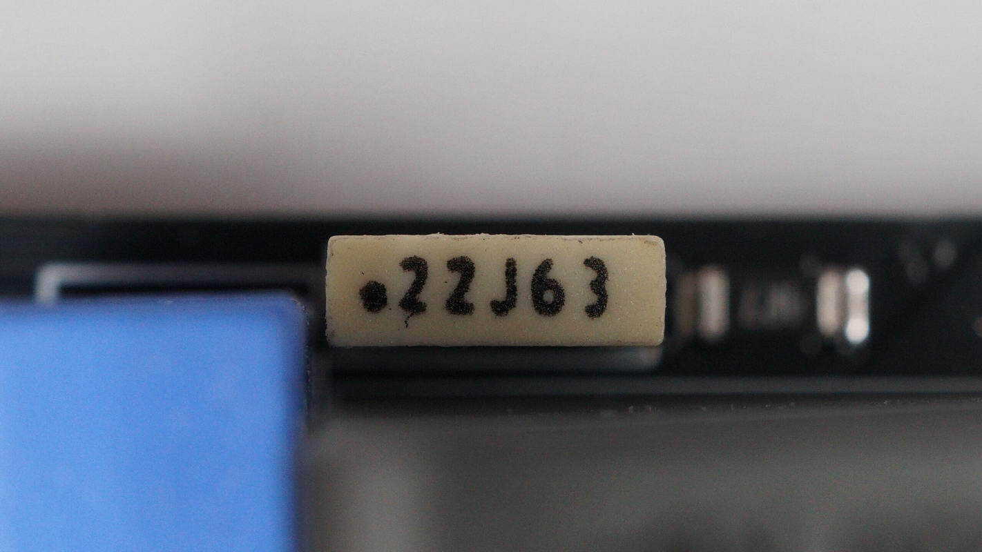
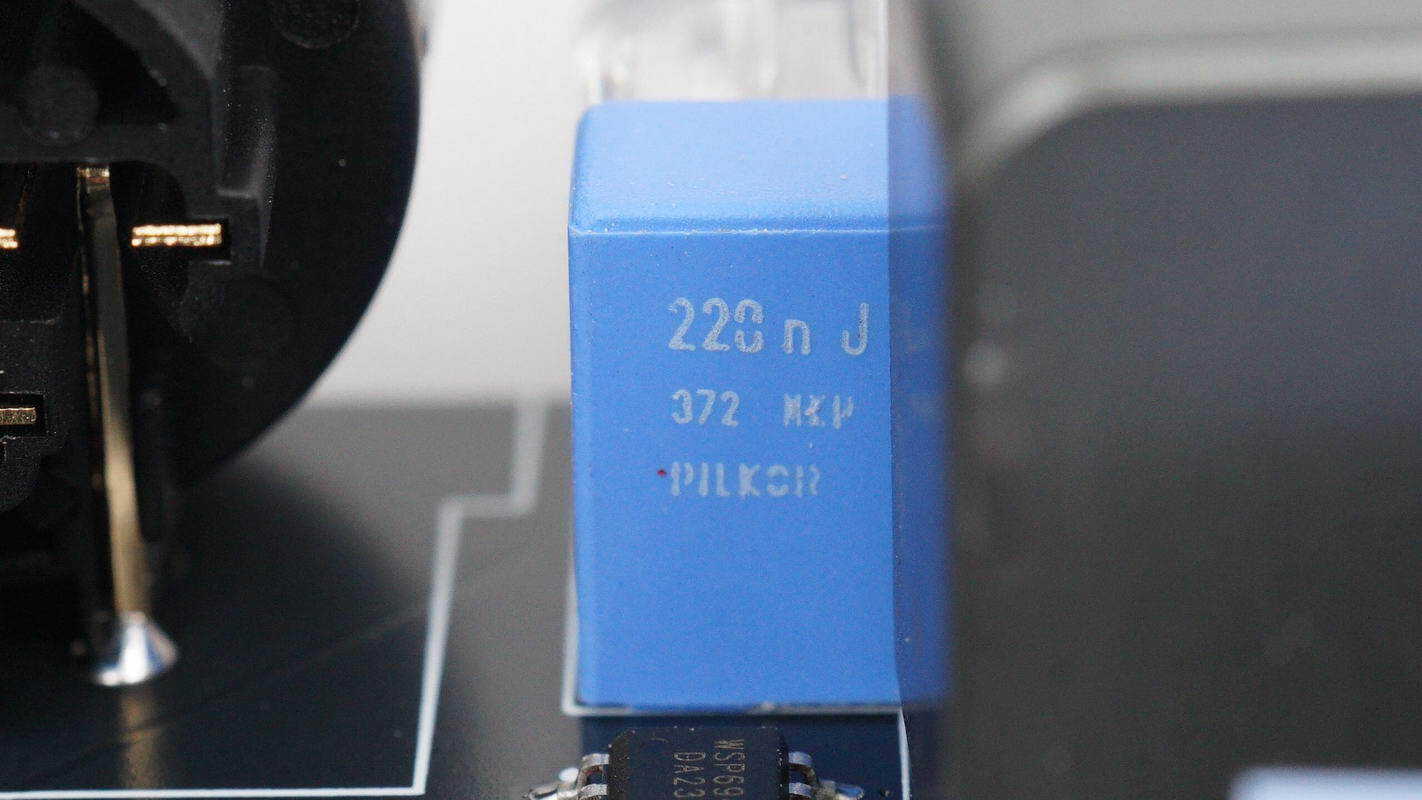
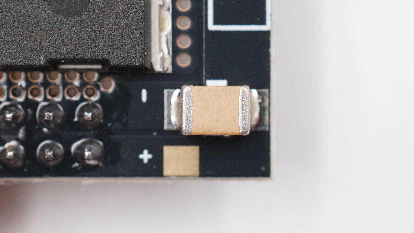
The film capacitor is rated at 0.22 μF, 63 V.
The film capacitor is from FILCO, rated at 0.22 μF.
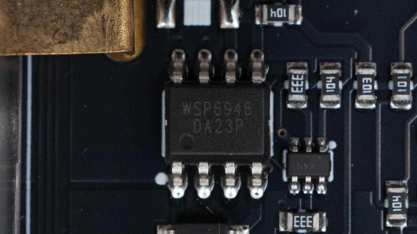
The MOSFET used for output control is from WINSOK, model WSP6946. It is a dual NMOS with a voltage rating of 60 V, an on-resistance of 33 mΩ, and comes in an SOP-8 package.
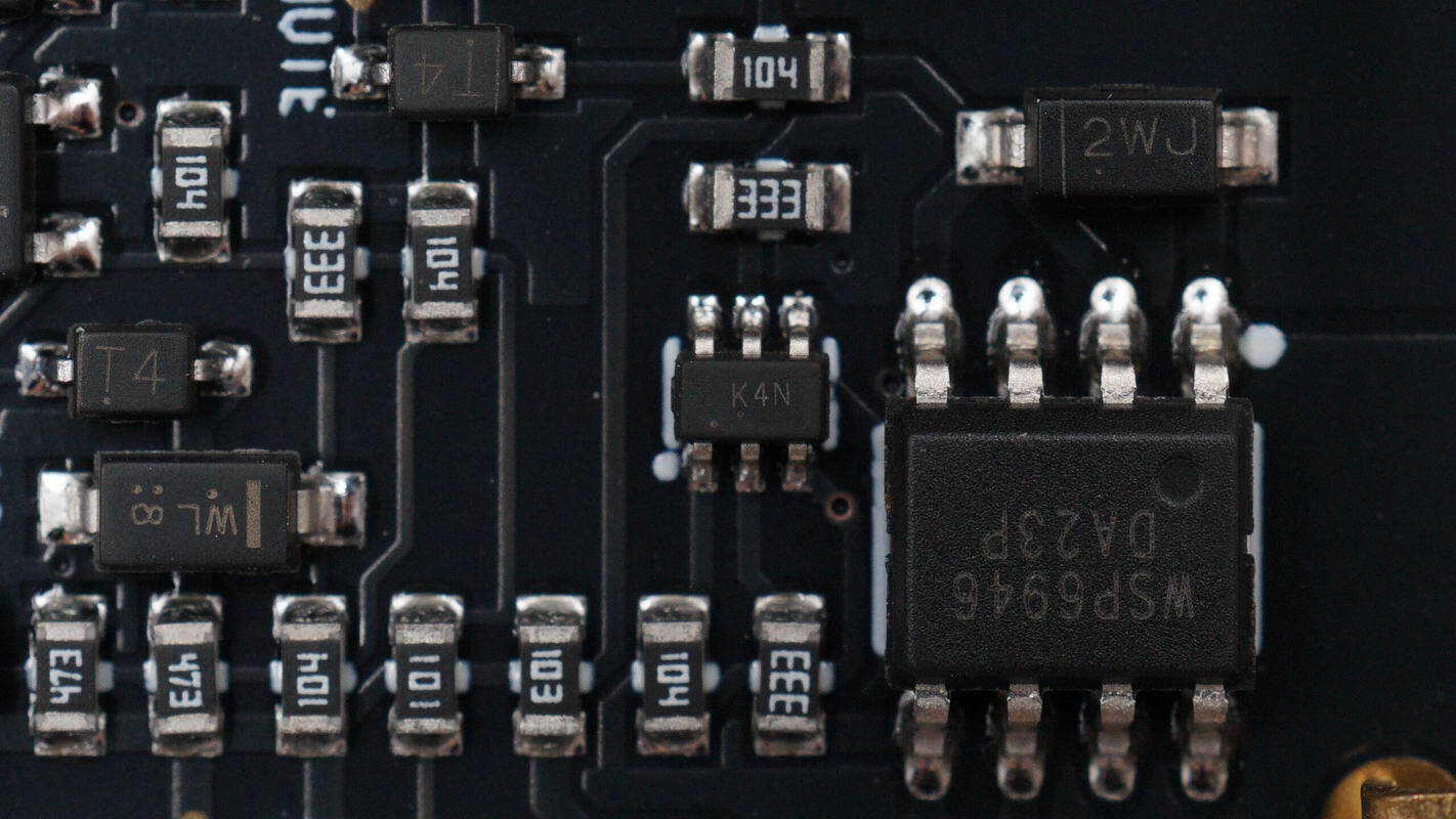
Close-up of the dual transistor marked K4N.
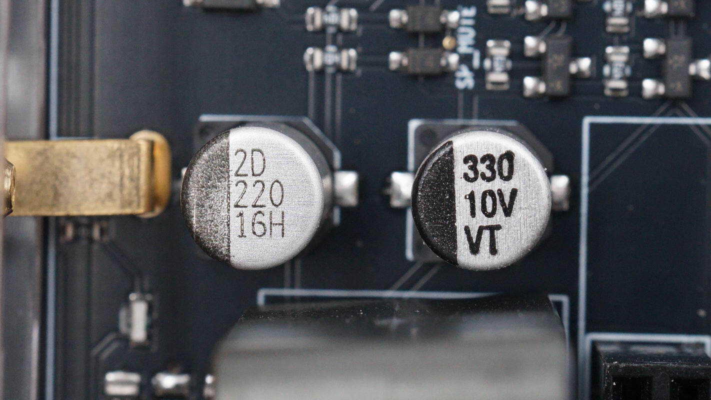
The filter capacitors are rated at 220 μF, 16 V, and 330 μF, 10 V, respectively.
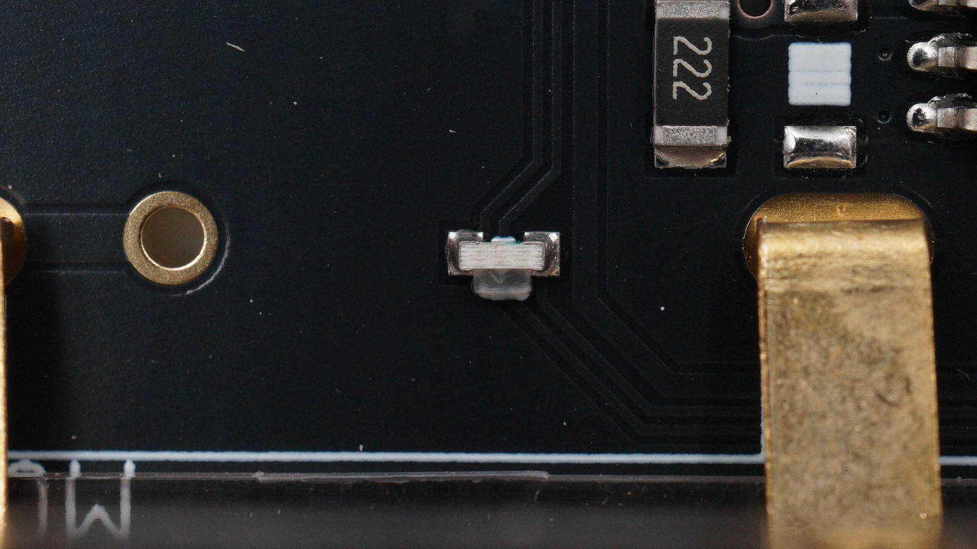
Close-up of the SMD LED used for operational indication.
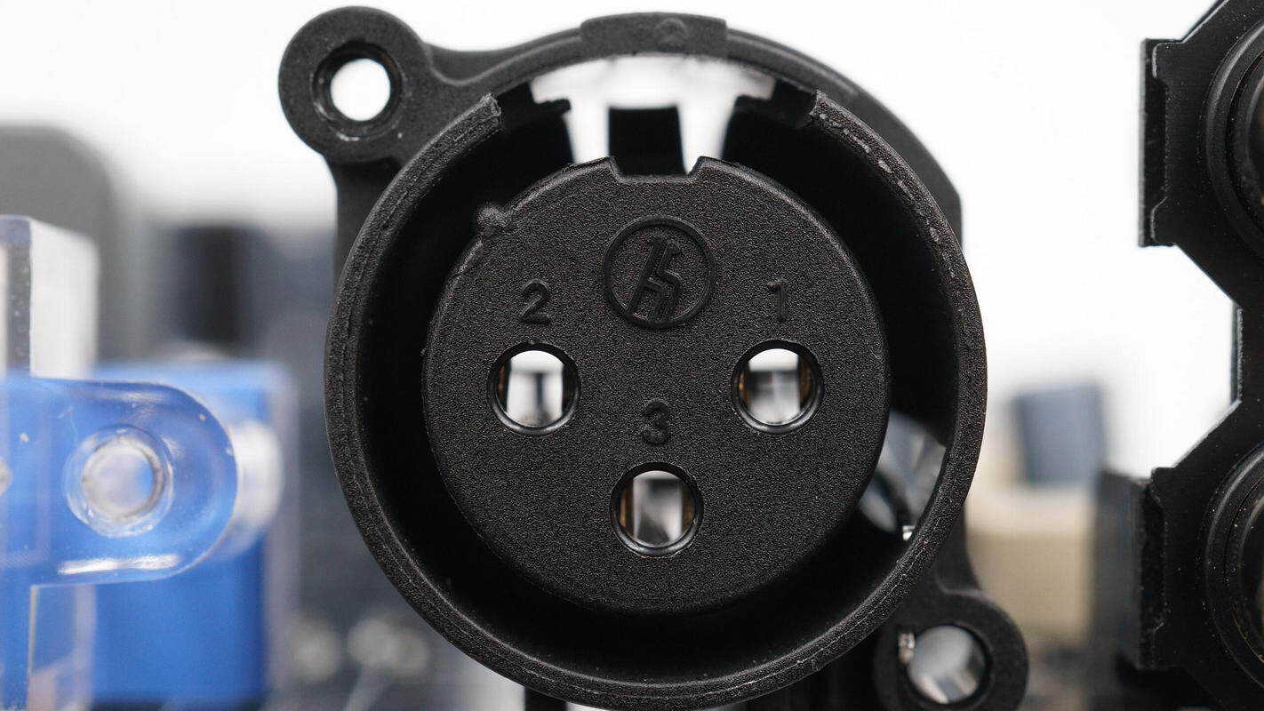
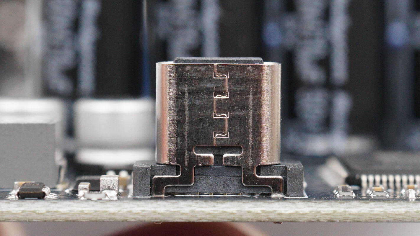
Close-up of the XLR input connector.
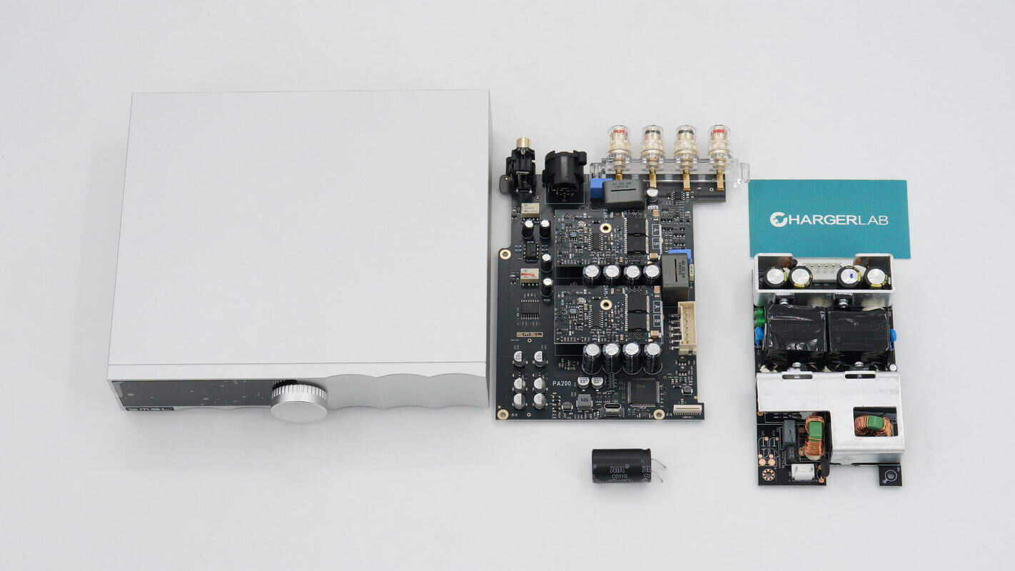
Well, those are all components of the SMSL GaN Power Amplifier.
Summary of ChargerLAB
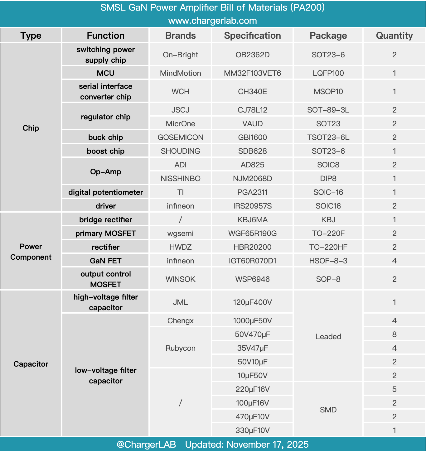
Here is the component list of the SMSL GaN Power Amplifier for your convenience.
It features an integrated aluminum alloy chassis. The front panel houses a display and a function knob, while the rear panel includes audio input jacks, speaker output connectors, and a power input socket. It supports a wide input voltage range of 100–240 V and offers both mono bridged and stereo modes.
After taking it apart, we found that it consists of a switching power supply module and a GaN amplifier module. The switching power supply uses two On-Bright OB2362D power supply chips, paired with WGSEMİ WGF65R190G MOSFETs and HWDZ HBR20200 rectifiers, forming a positive and negative power supply module that provides power to the GaN amplifier module.
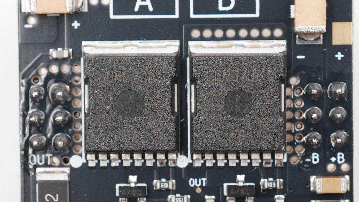
The GaN amplifier module uses Infineon IGT60R070D1 GaN FETs, driven by Infineon IRS20957S drivers, and employs ADI AD825 operational amplifiers. The MCU is a MindMotion MM32F103VET6, the digital potentiometer is a Texas Instruments PGA2311, and the NISSHINBO NJM2068D op-amp is used for pre-amplification.
On the underside of the GaN amplifier PCB, a thermal pad and an aluminum block are installed. A partition separates the power supply module and amplifier module, and HONGFA relays are used for audio signal switching. The build quality is solid, with reliable components.
Related Articles:
1. Teardown of RedMagic 80W Air-Cooled Wireless Charging Dock (PA0404)
2. Teardown of Momax 45W 3-in-1 GaN Power Bank with Retractable Cable (IP167)
3. Teardown of Maxcellent Multi-Function Portable Jump Starter