Introduction
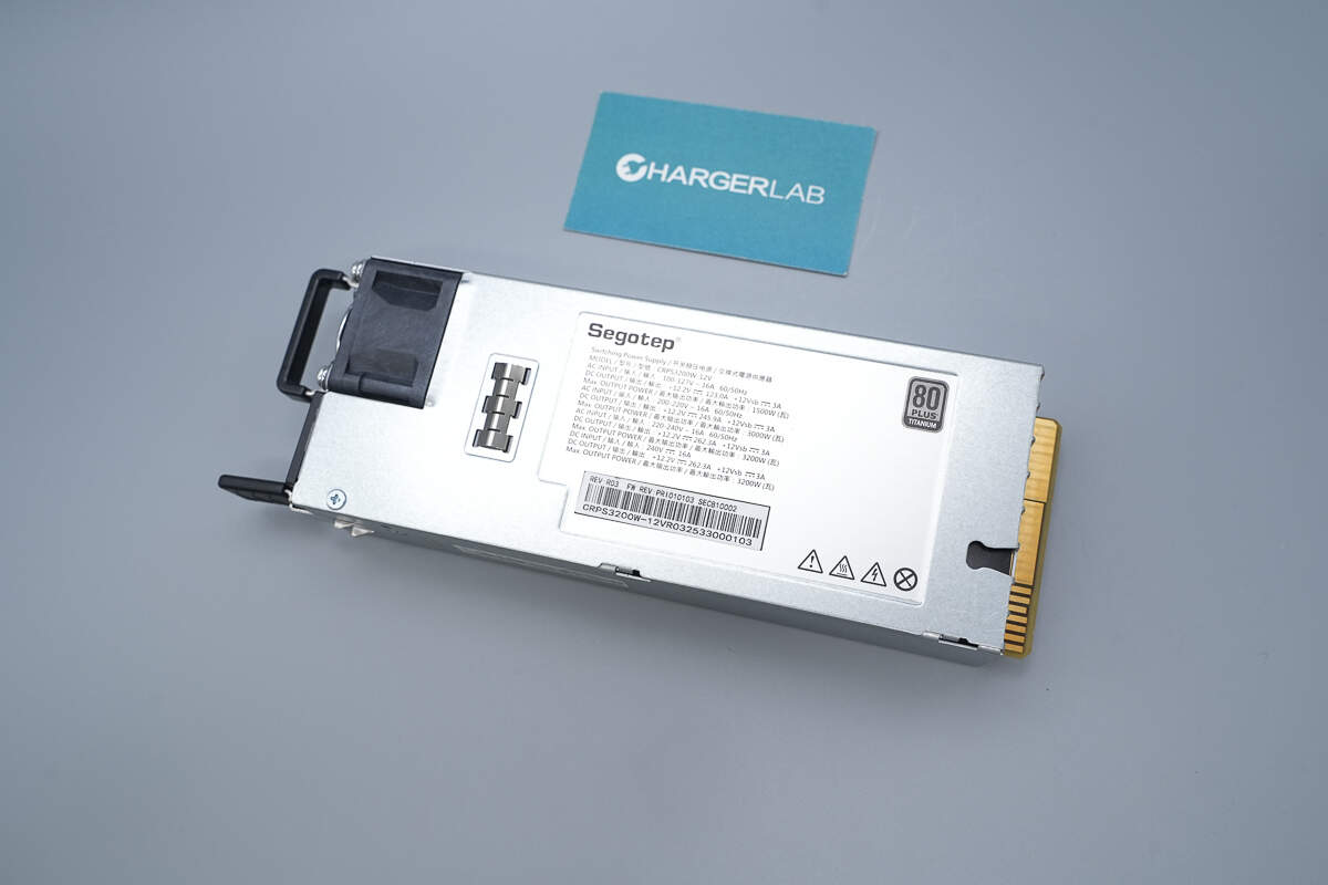
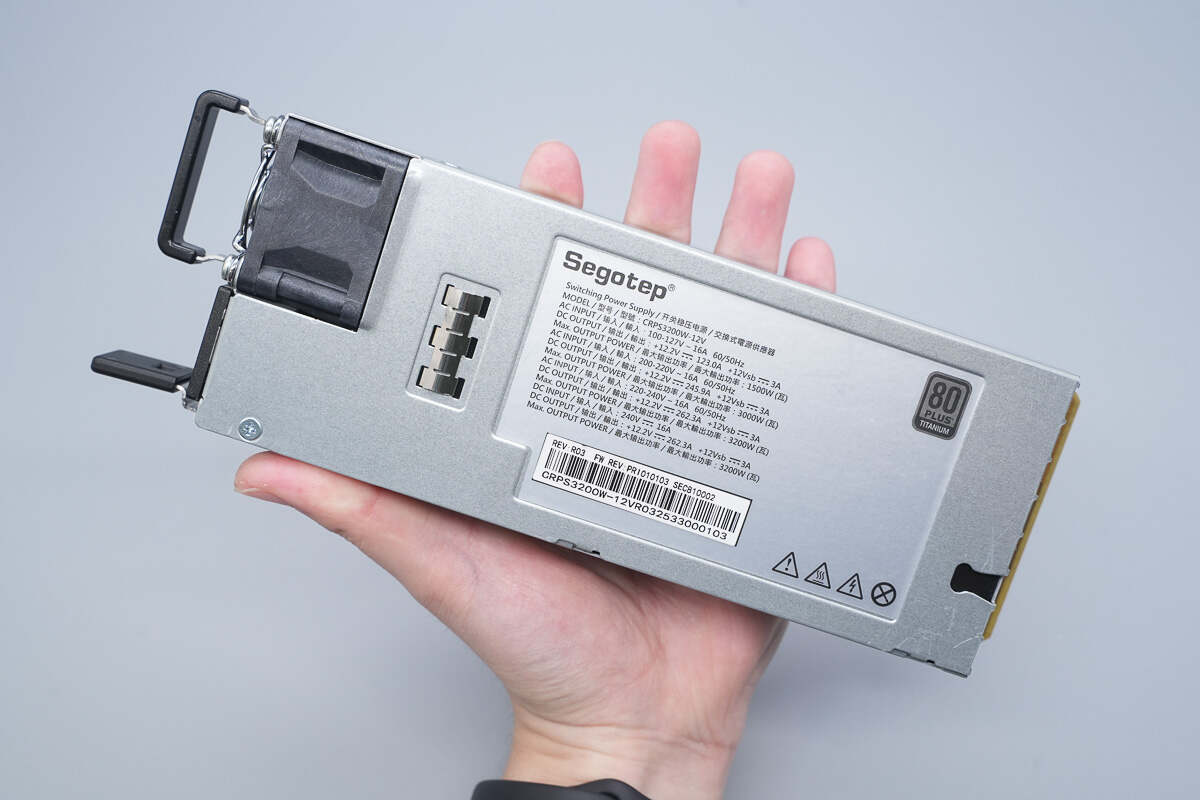
We obtained Segotep’s newly released 3200W Titanium-rated SiC digital power supply. This unit follows the standard CRPS form factor and adopts a fully digital control solution from Texas Instruments. It integrates two DSP chips—one dedicated to interleaved totem-pole PFC control and the other for full-bridge LLC control. The model designation is CRPS3200W-12V, and it supports a wide input voltage range.
Segotep is positioning itself in the high-end CRPS market by emphasizing modularity and standardization to achieve broad compatibility. The design consists of eight PCB modules, scalable up to 5.5 kW at 54 V output (including DSP algorithm optimization). Each module is manufactured using a fully automated SMT process, with a heatsink-free and pre-processing-free design. The DSP-based modular architecture allows minor upgrades to support higher power ratings and even three-phase input configurations in the future. This approach enables rapid product development based on a unified technical platform, minimizing validation and investment time while allowing customization of specific modules to meet individual client requirements.
The power supply delivers a rated output of 12.2 V at 262.3 A, with an auxiliary standby output of 12 V at 3 A. It features a long rectangular metal chassis, and the totem-pole PFC stage employs Infineon silicon carbide MOSFETs. The following teardown provides an in-depth look at the internal layout, design approach, and component selection.
Product Appearance
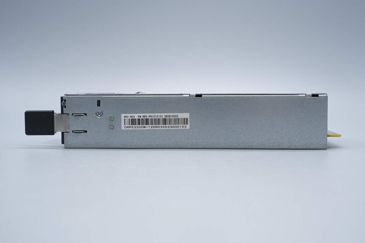
The front side of the metal case has a label.
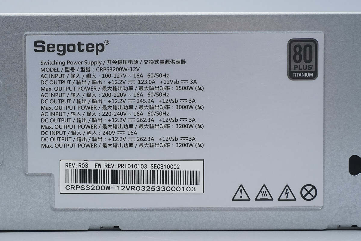
Model: CRPS3200W-12V
AC Input: 100–127V~ 16A 60/50Hz
DC Output: +12.2V 123A, +12Vsb 3A
Maximum Output Power: 1500W
AC Input: 200–220V~ 16A 60/50Hz
DC Output: +12.2V 245.9A, +12Vsb 3A
Maximum Output Power: 3000W
AC Input: 220–240V~ 16A 60/50Hz
DC Output: +12.2V 262.3A, +12Vsb 3A
Maximum Output Power: 3200W
DC Input: 240V 16A
DC Output: +12.2V 262.3A, +12Vsb 3A
Maximum Output Power: 3200W
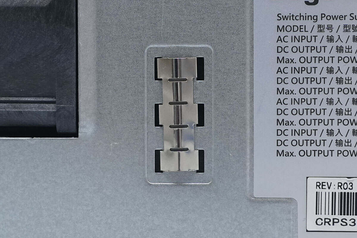
The springs on the front side are used for grounding.
Springs are also provided on the rear side.
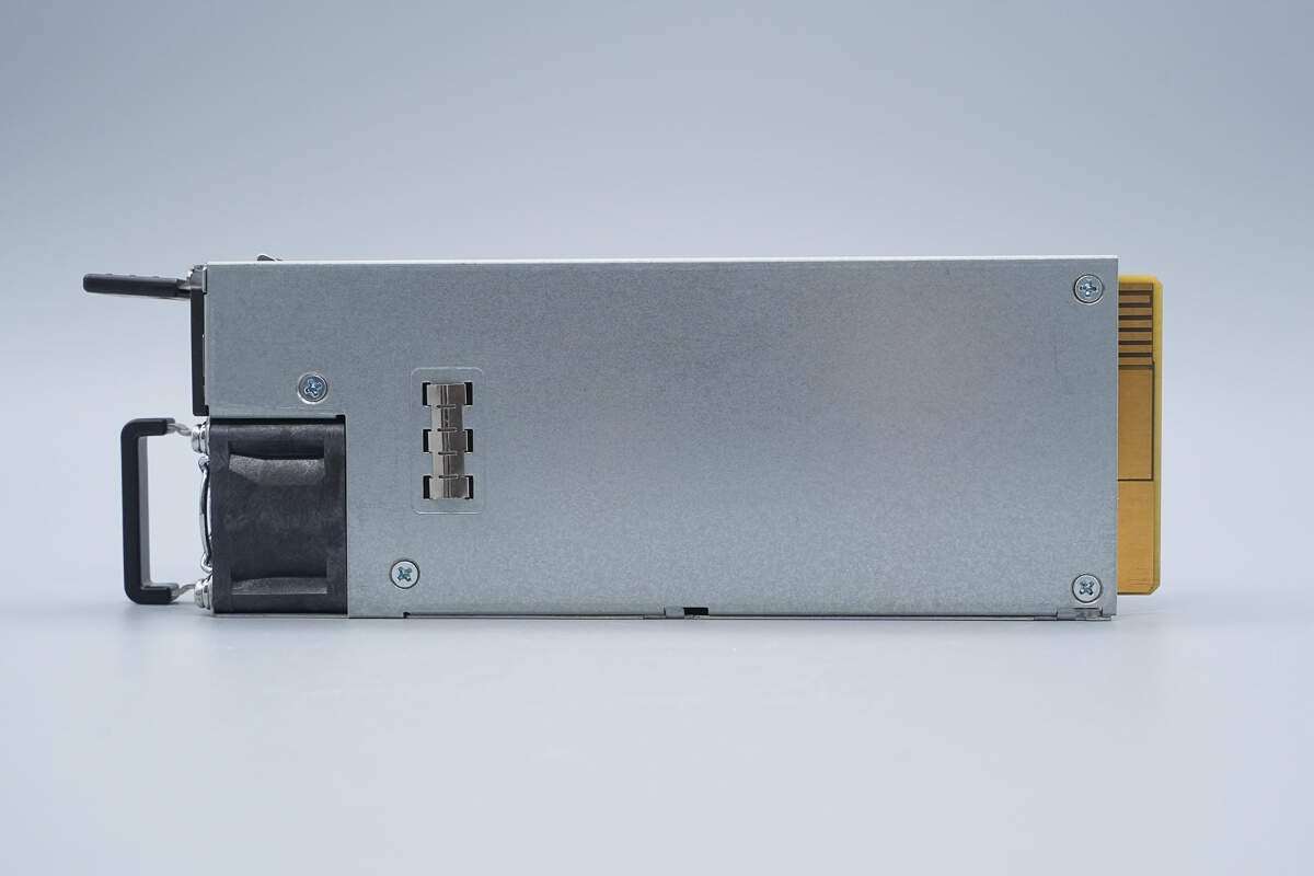
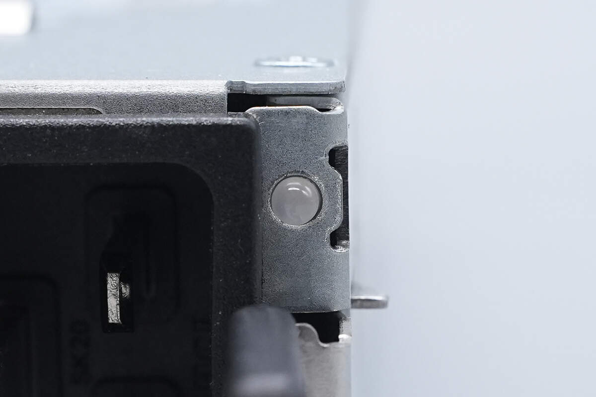
The side is equipped with latches and screws.
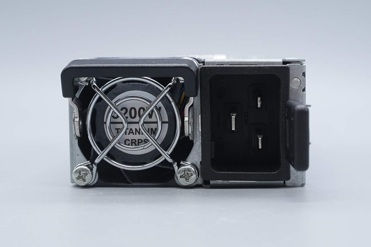
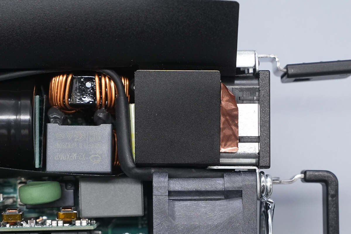
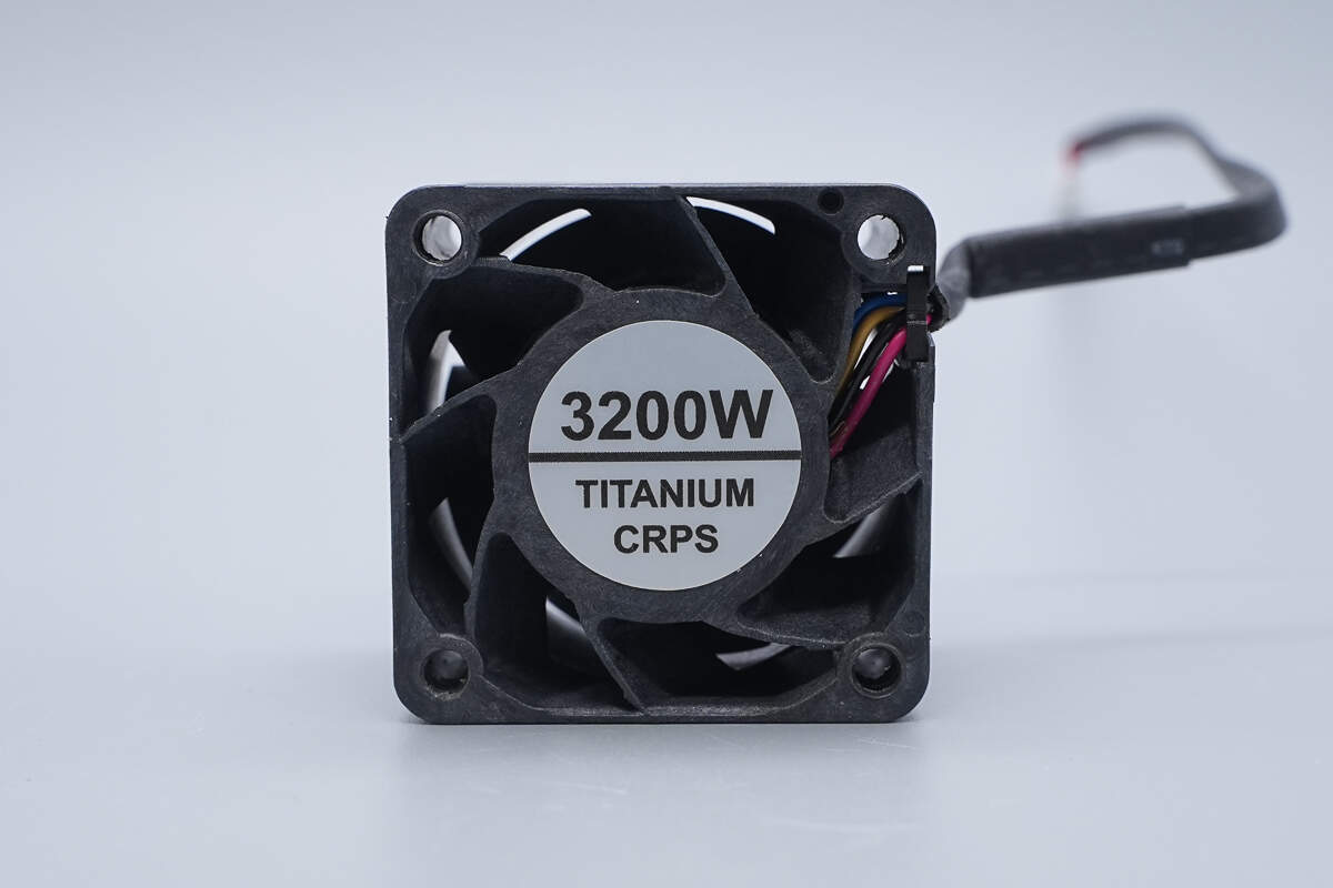
The input side is equipped with a handle, cooling fan, input socket, power indicator, and release lever.
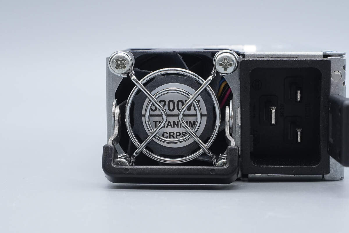
The fan guard is labeled with “3200W,” “TITANIUM,” and “CRPS.”
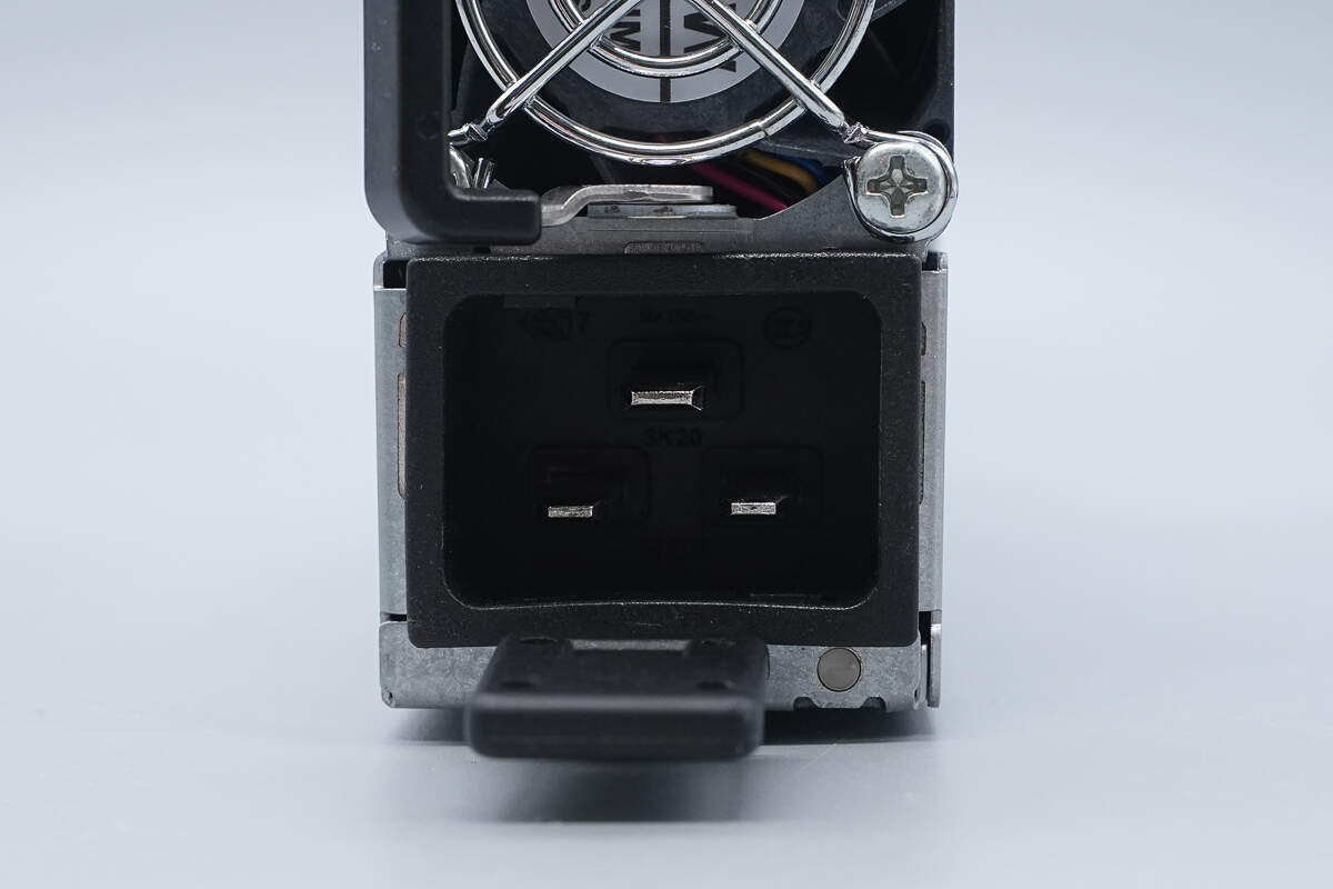
The input socket is a C20 type.
Close-up of the LED indicator light.
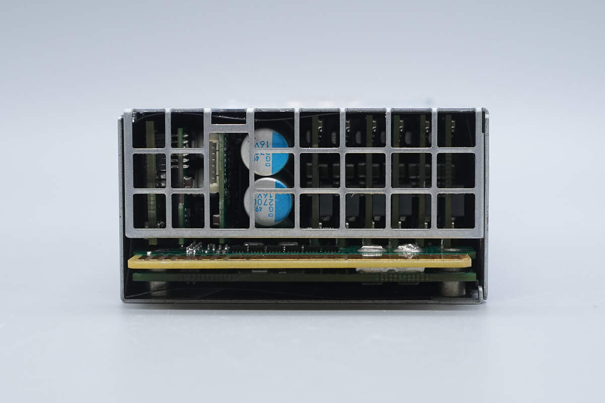
The output side features a grille and a gold-finger PCB.
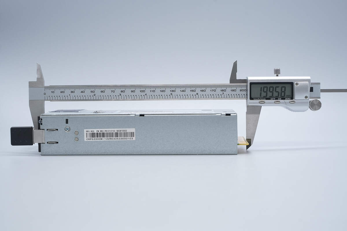
The length of the module is about 199.6 mm (7.86 inches).
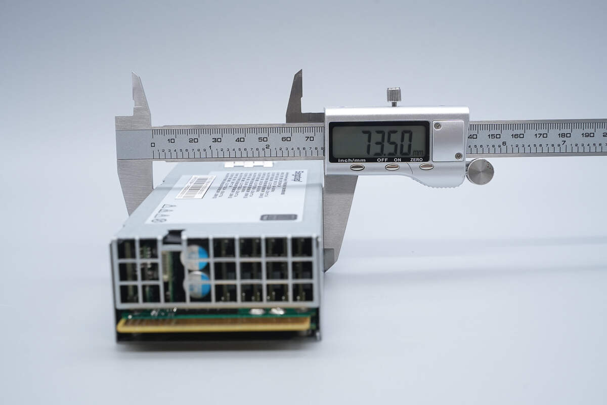
The width is about 73.5 mm (2.89 inches).
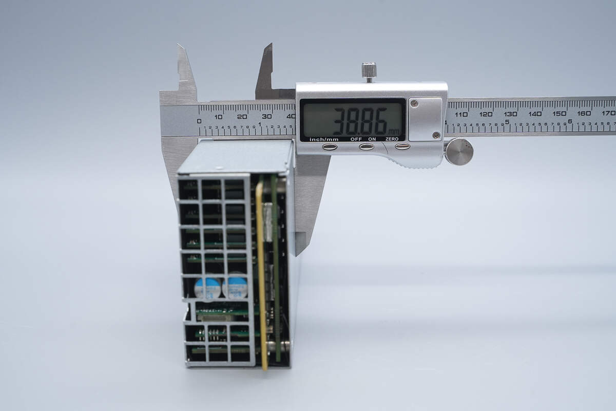
The thickness is about 38.9 mm (1.53 inches).
That's how big it is in the hand.
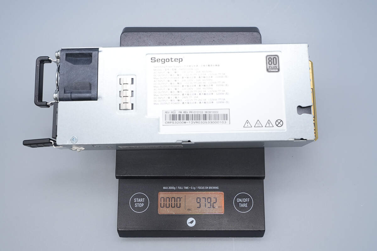
The weight is about 979 g (34.53 oz).
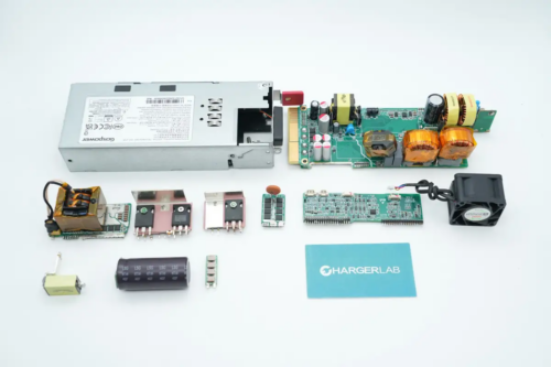
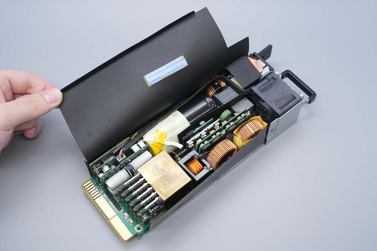
Teardown
Next, let's take it apart to see its internal components and structure.
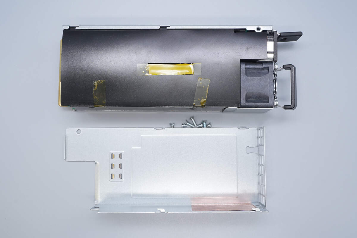
Unscrew the screws to remove the housing.
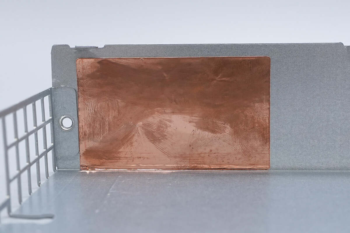
Copper foil inside the housing is used for shielding.
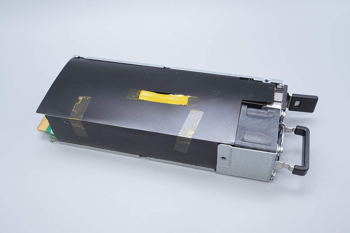
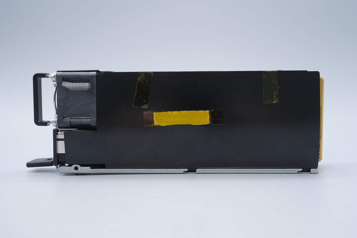
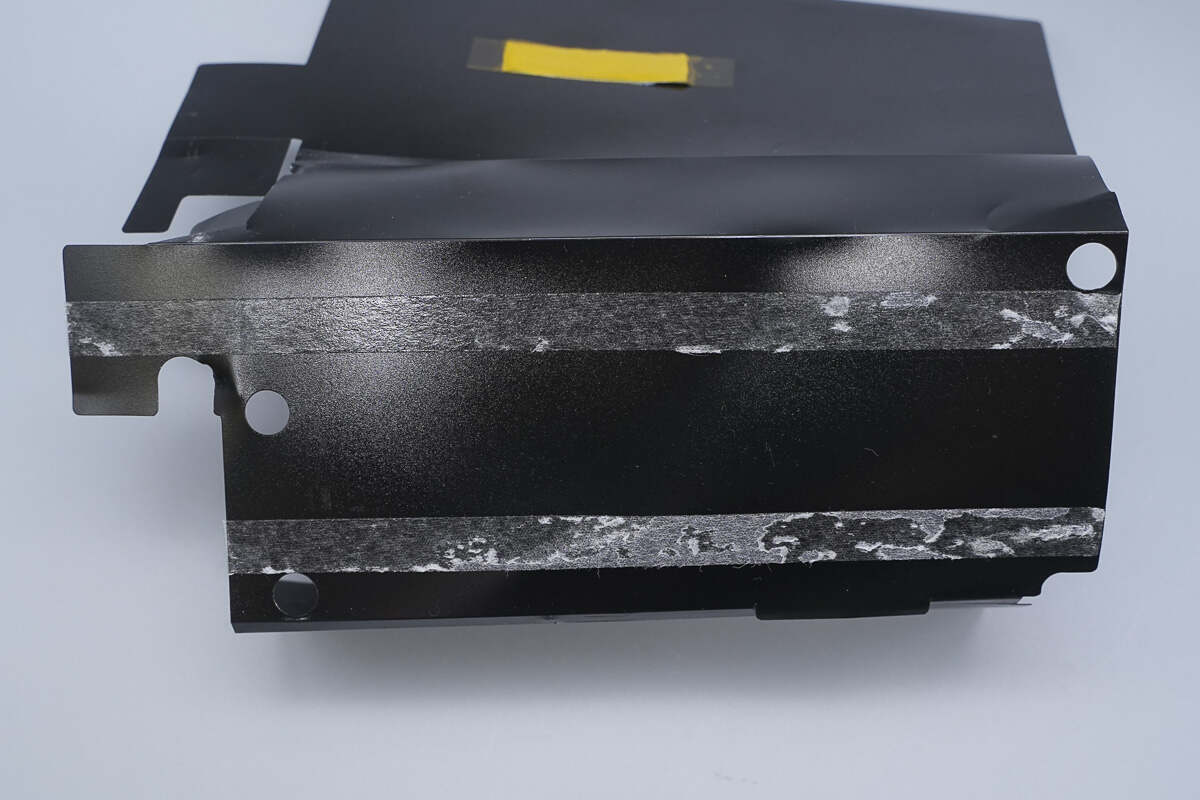
The PCBA module is wrapped in black Mylar for insulation and secured with tape.
A thermal pad is placed at the opening.
The thermal pad corresponds to the small PCBs.
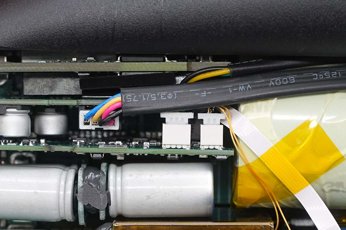
Close-up of the connectors for the cooling fan, indicator light, and current transformer.
The input socket is insulated with a Mylar sheet.
The socket is connected via wires.

The PCB for driving LLC MOSFETs is connected to the control PCB via a ribbon cable.
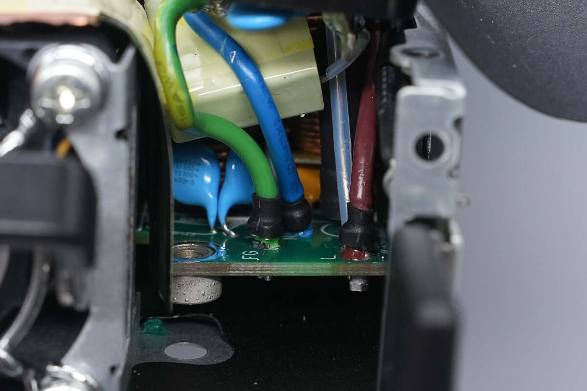
The input wires are connected by soldering.
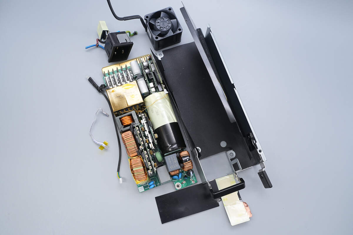
Unscrew the screws and remove the PCBA module.
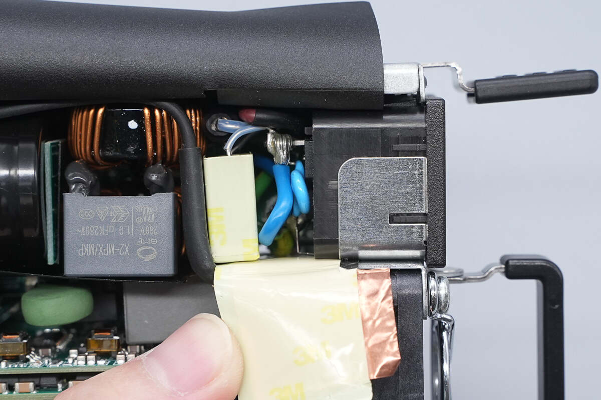
The Mylar sheet is secured with double-sided adhesive tape.
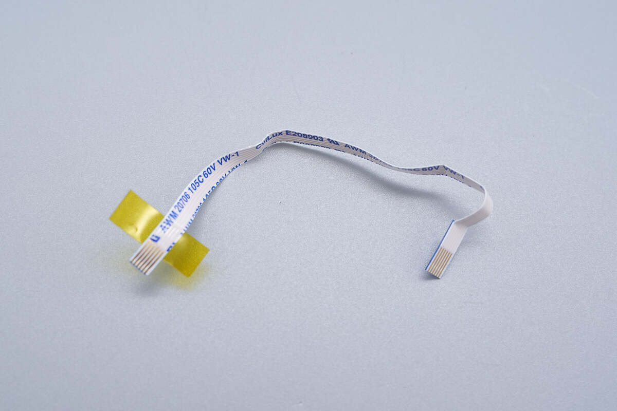
Close-up of the ribbon cable.
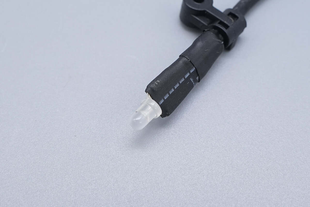
The LED indicator is insulated with a heat-shrink tube.
The cooling fan has fixed blades.
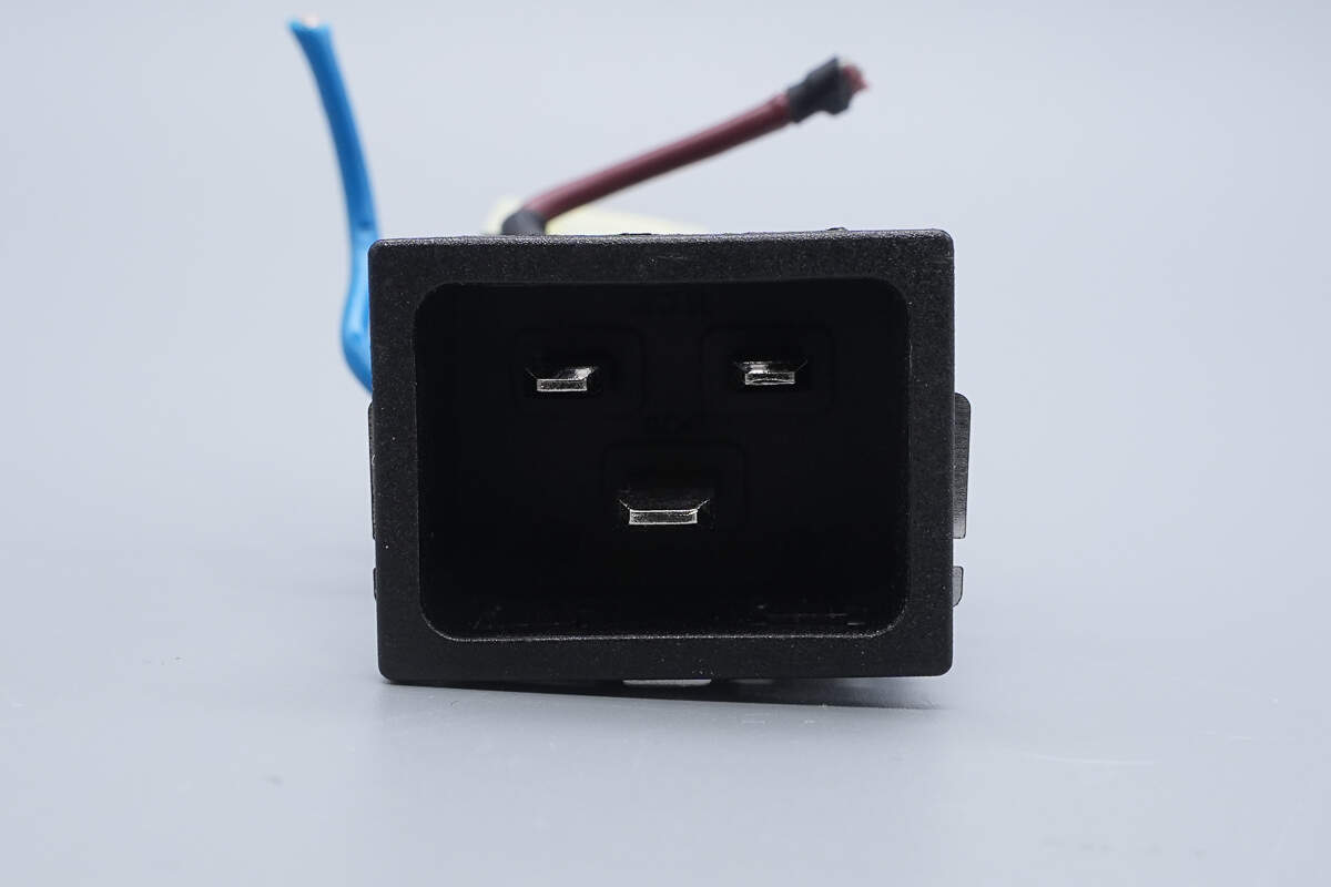
Close-up of the C20 input socket.
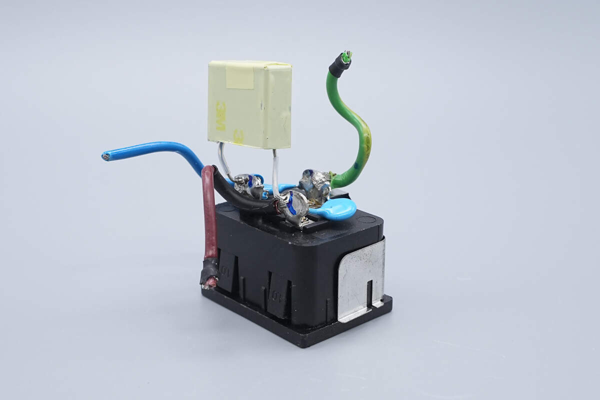
The back of the socket is equipped with blue Y capacitors and a safety X2 capacitor.
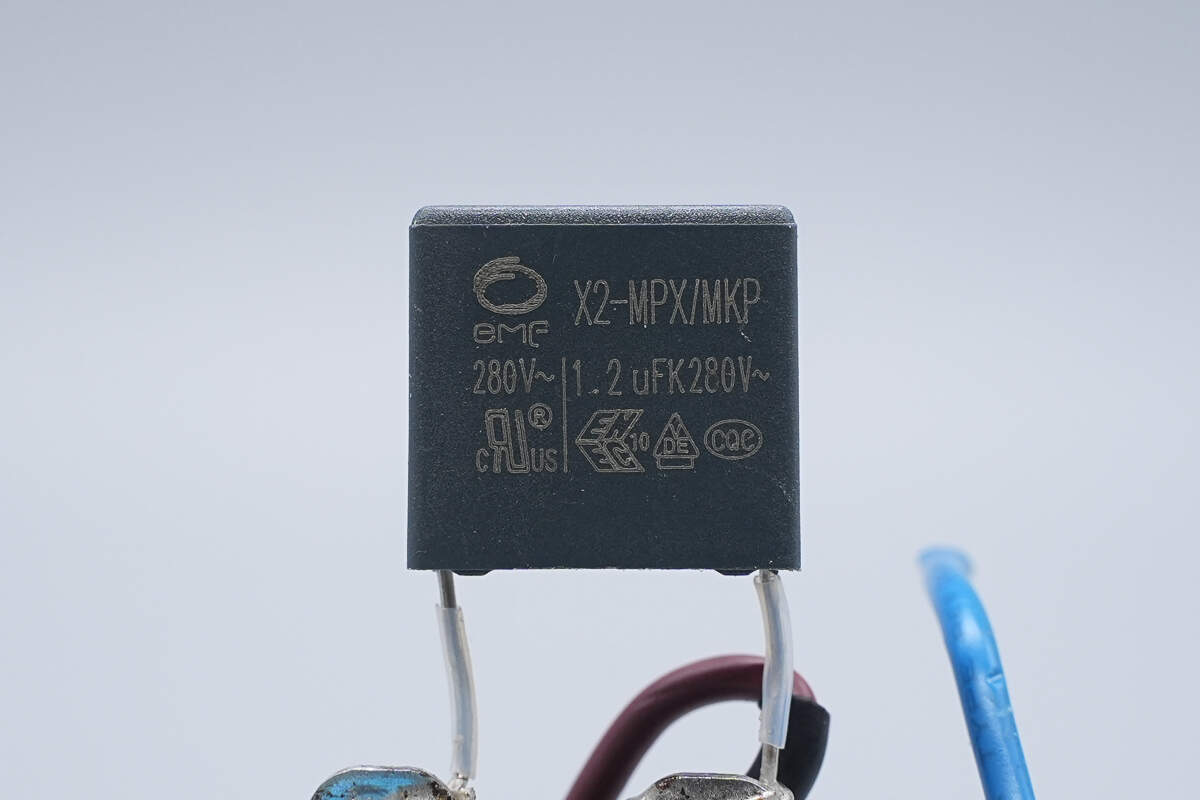
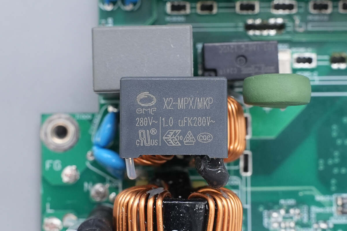
The safety X2 capacitor is from EMF, with a specification of 1.2 μF.
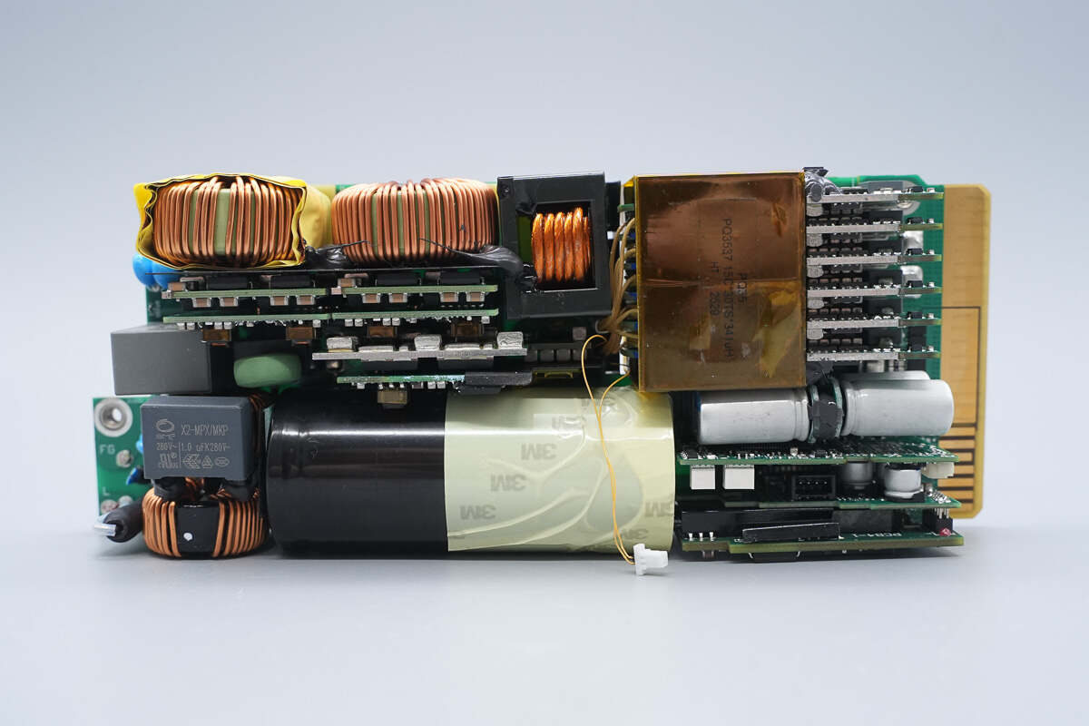
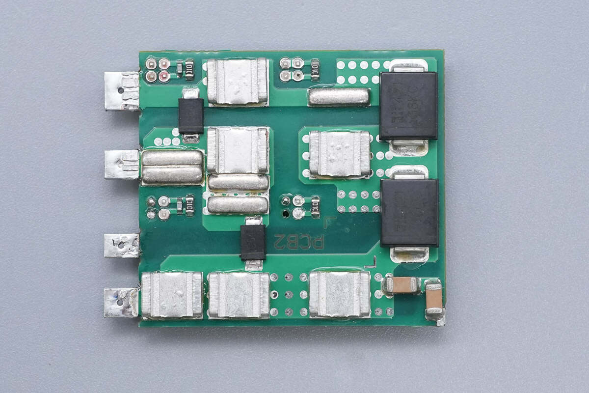
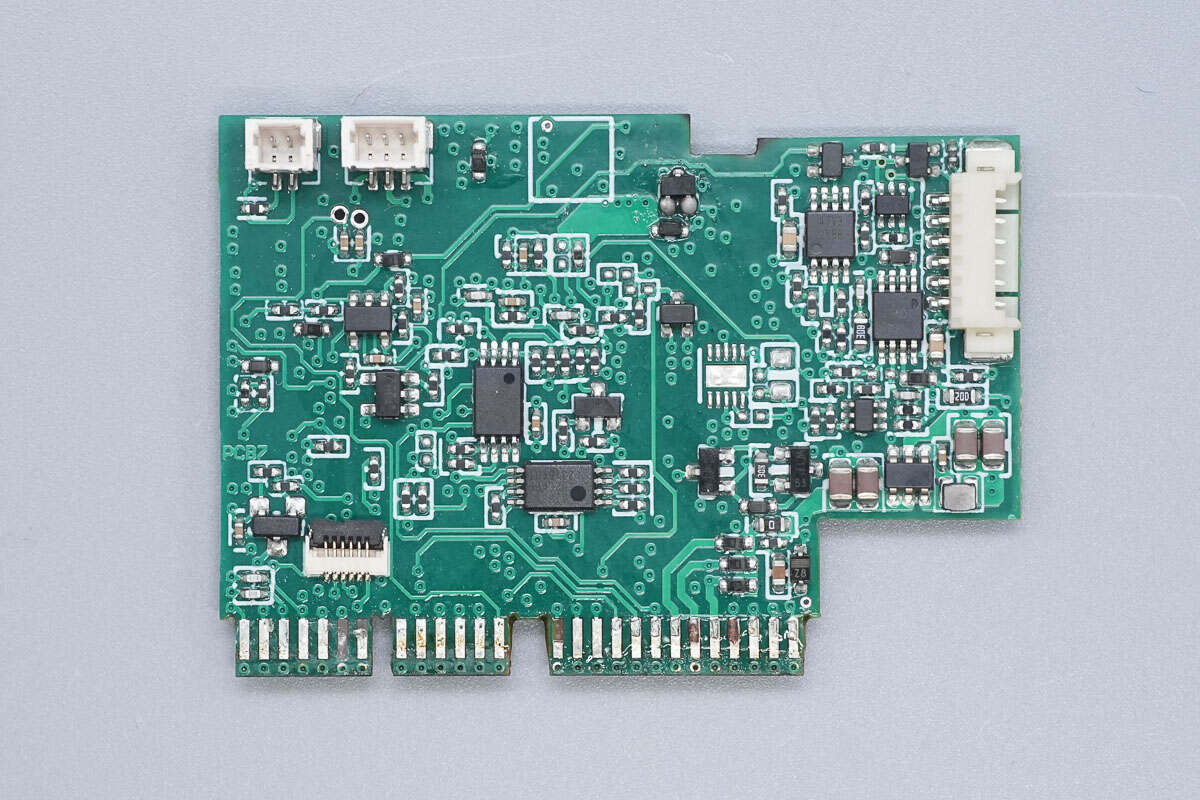
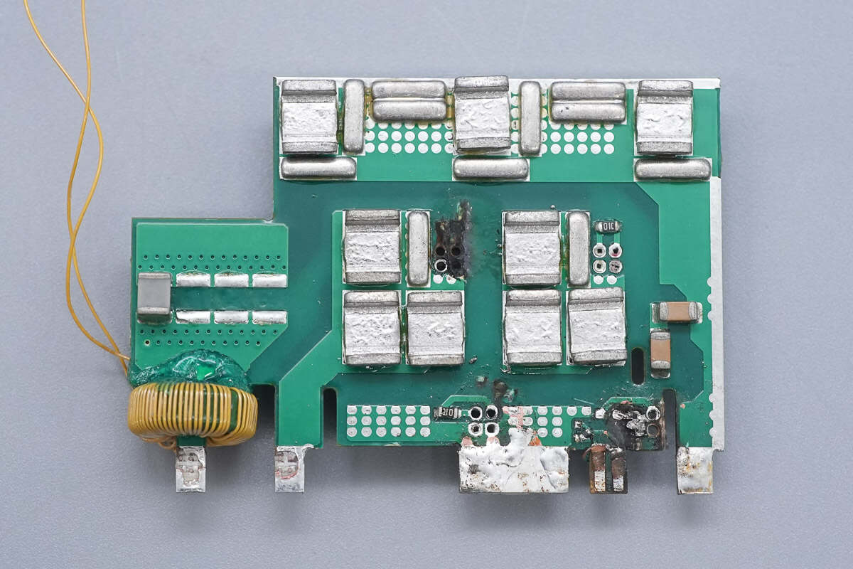
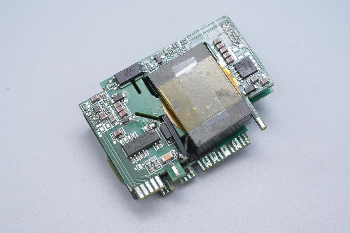
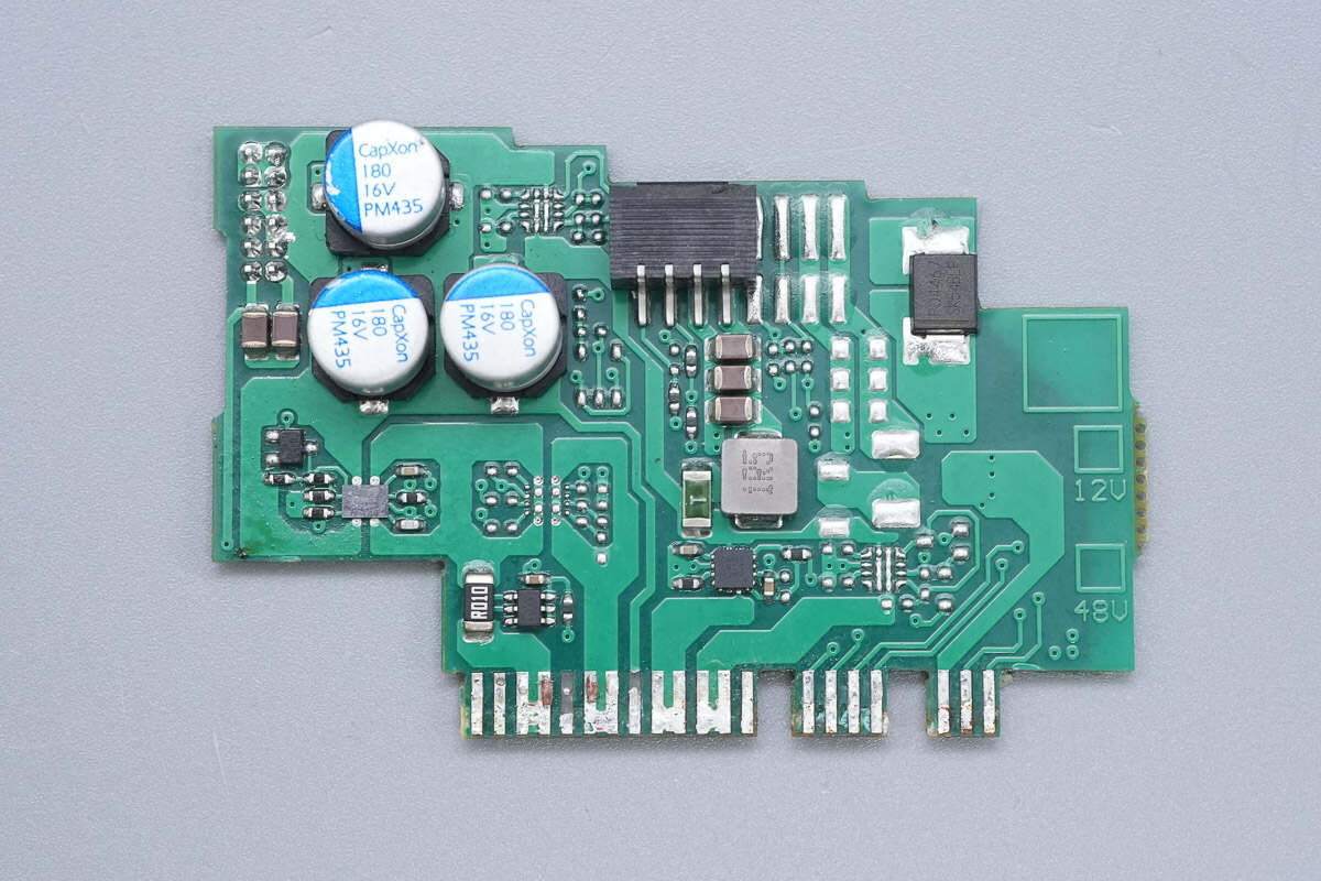
The front side of the PCBA module contains components such as a fuse, common mode choke, safety X2 capacitor, Totem-pole PFC MOSFET, PFC boost inductor, LLC MOSFET, high-voltage filter capacitor, LLC resonant inductor, LLC transformer, solid capacitors, and other related components.
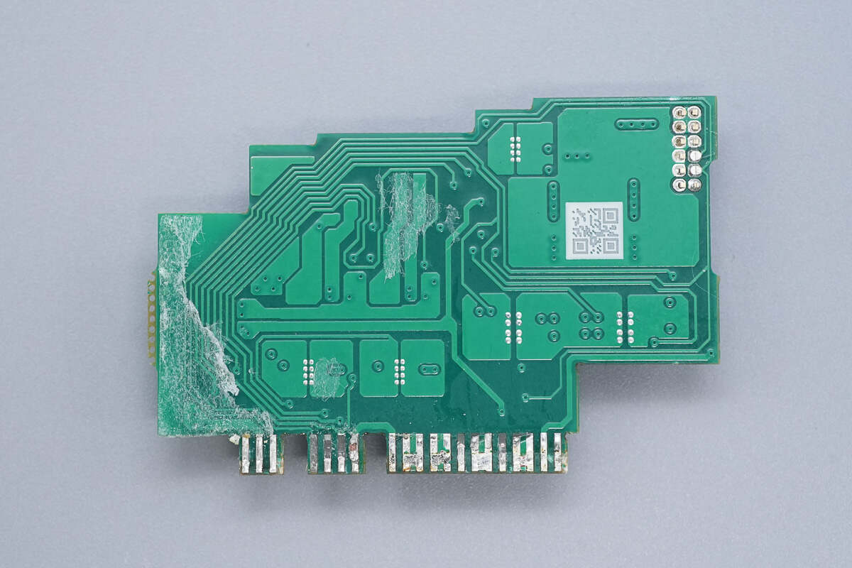
The back side contains a current-sensing chip, PFC controller, isolation communication chip, and other components.
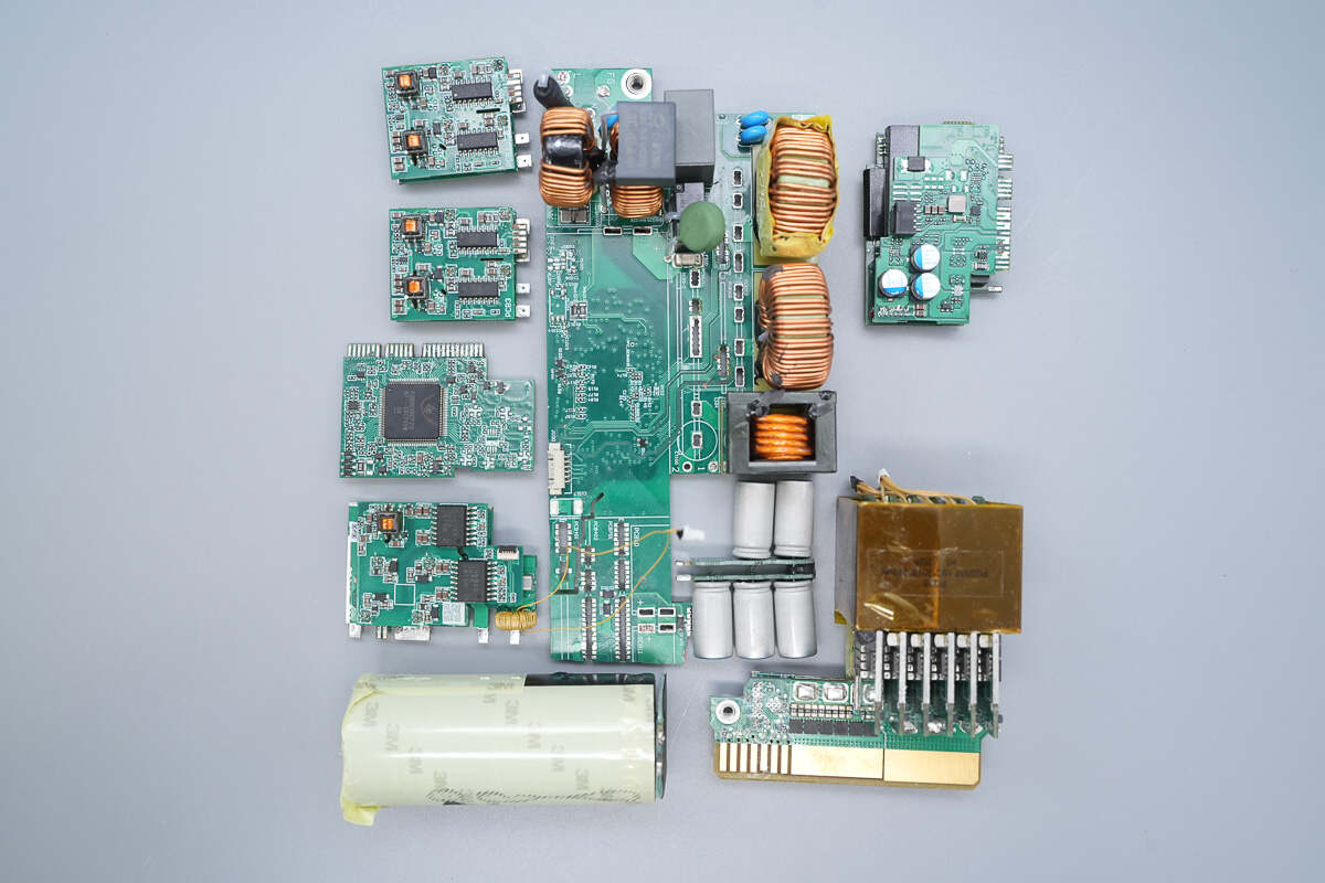
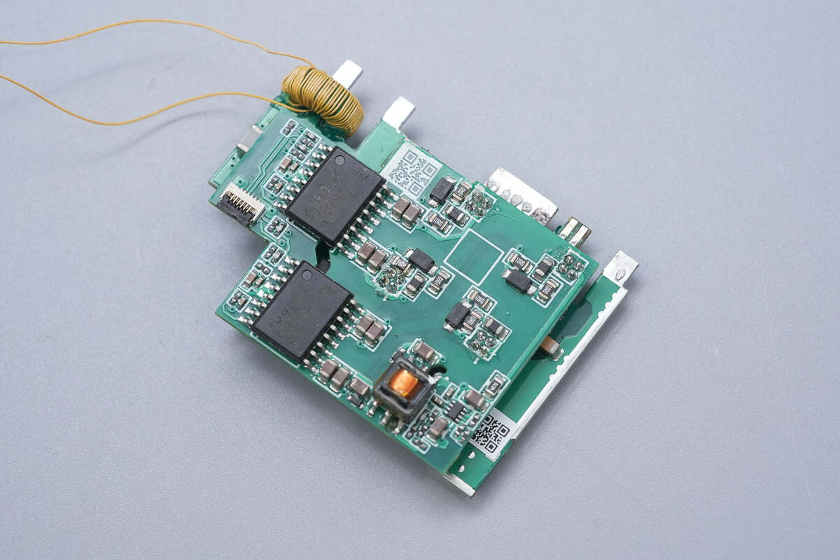
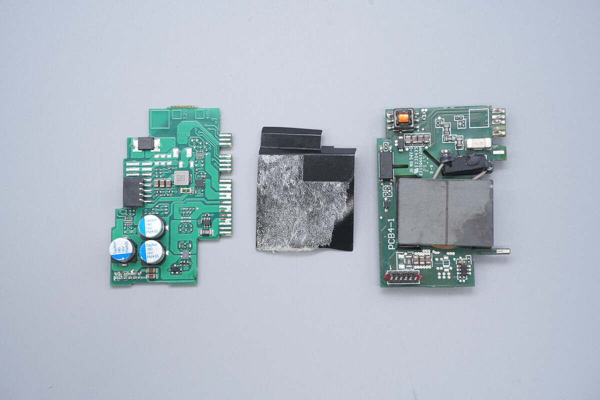
Remove the PFC MOSFET PCB, LLC MOSFET PCB, standby power PCB, LLC control PCB, high-voltage filter capacitor, and output transformer.
The input fuse is insulated with a heat-shrink tube.

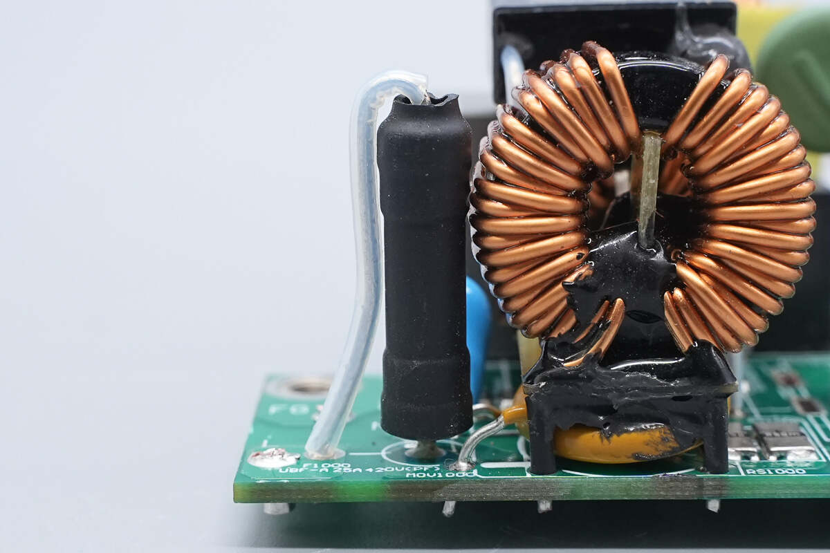
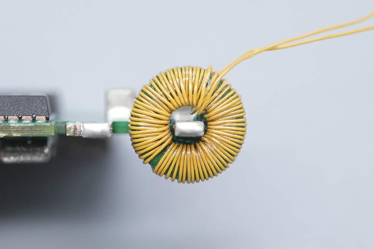
The common mode choke is wound with enameled wire, with a varistor and a current-sensing resistor installed at the bottom.
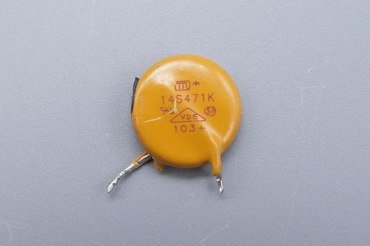
The varistor is from JOYIN, model 14S471K, used to absorb overvoltage surges.
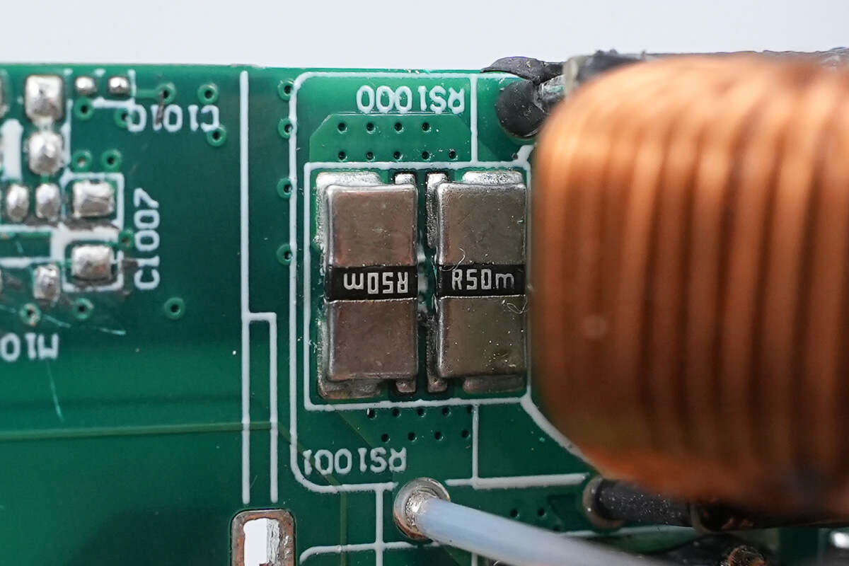
Two 0.5 mΩ sensing resistors are connected in parallel to measure the input current.
The safety X2 capacitor is from EMF, with a specification of 1 μF.
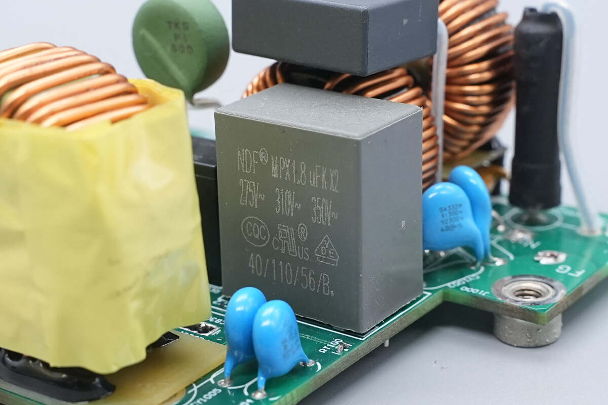
Another safety X2 capacitor is from NDF, with a specification of 1.8 μF.
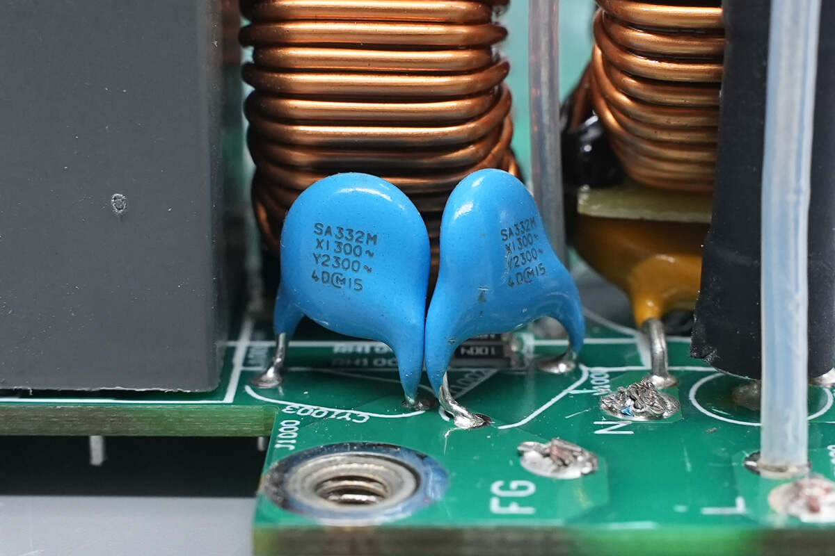
The blue Y capacitors are from MURATA.
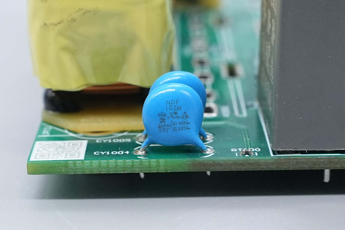
These two blue Y capacitors are from NDF.
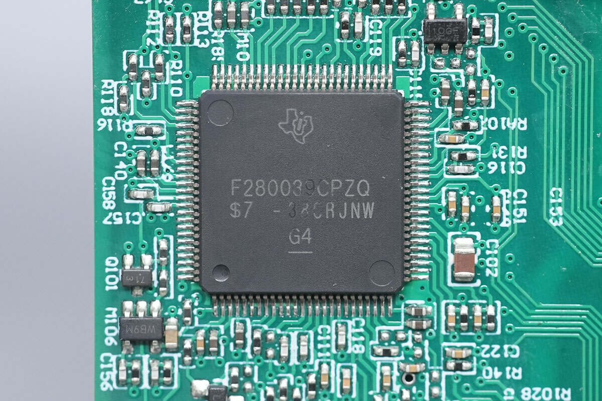
The PFC controller is from TI, model TMS320F280039C-Q1. It features a built-in C28x DSP core and an integrated programmable control-law accelerator, with a main frequency of 120 MHz, 384 KB of FLASH, and 69 KB of RAM. It includes high-performance analog modules and offers 16 PWM channels. The controller supports PMBus, I2C, CAN, SPI, SCI, LIN, and FSI interfaces, configurable logic blocks, and a host-interface controller. It comes in an LQFP100 package.
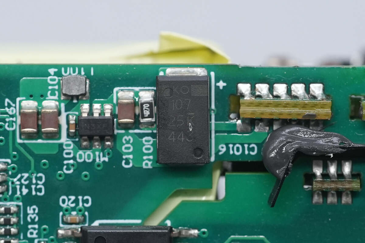
The filter capacitor is from KEMET, with a specification of 100 μF, 25 V.
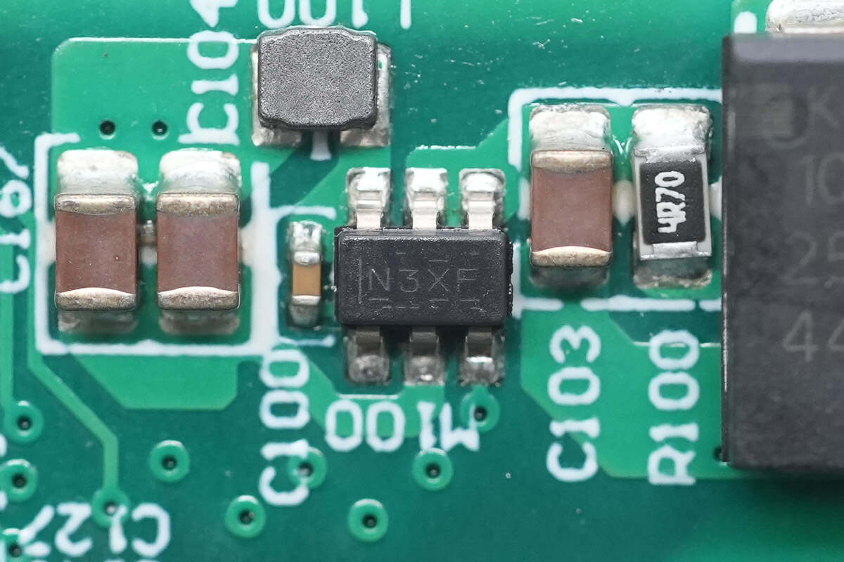
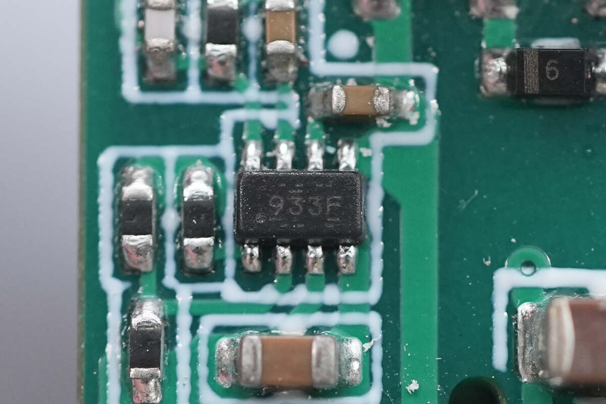
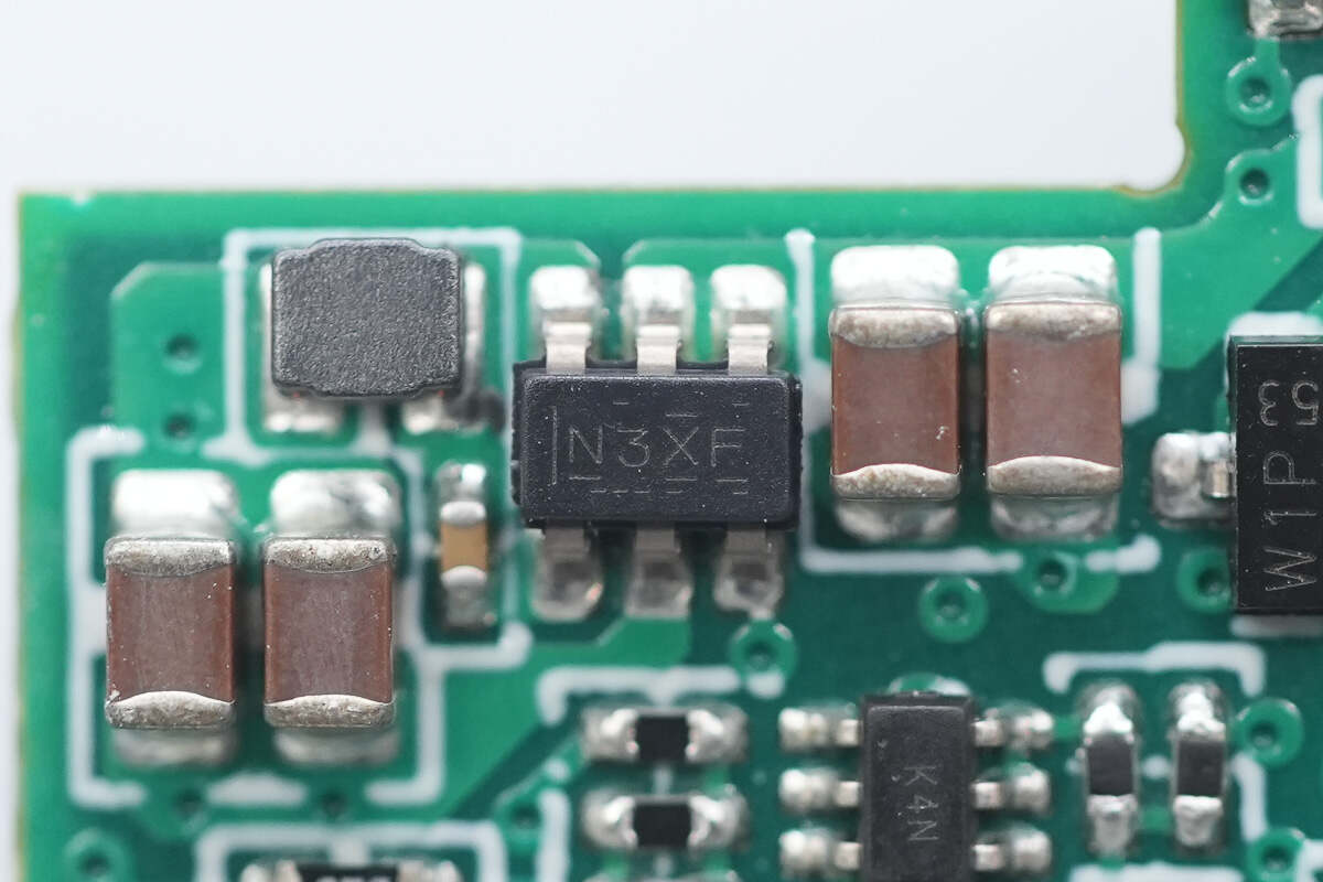
The synchronous buck chip is from TI, marked N3XF, model TPS560430X3F. It supports an input voltage of 4–36 V, outputs 3.3 V at 600 mA, operates at a switching frequency of 1.1 MHz in FPWM mode, and comes in a SOT-23 package.
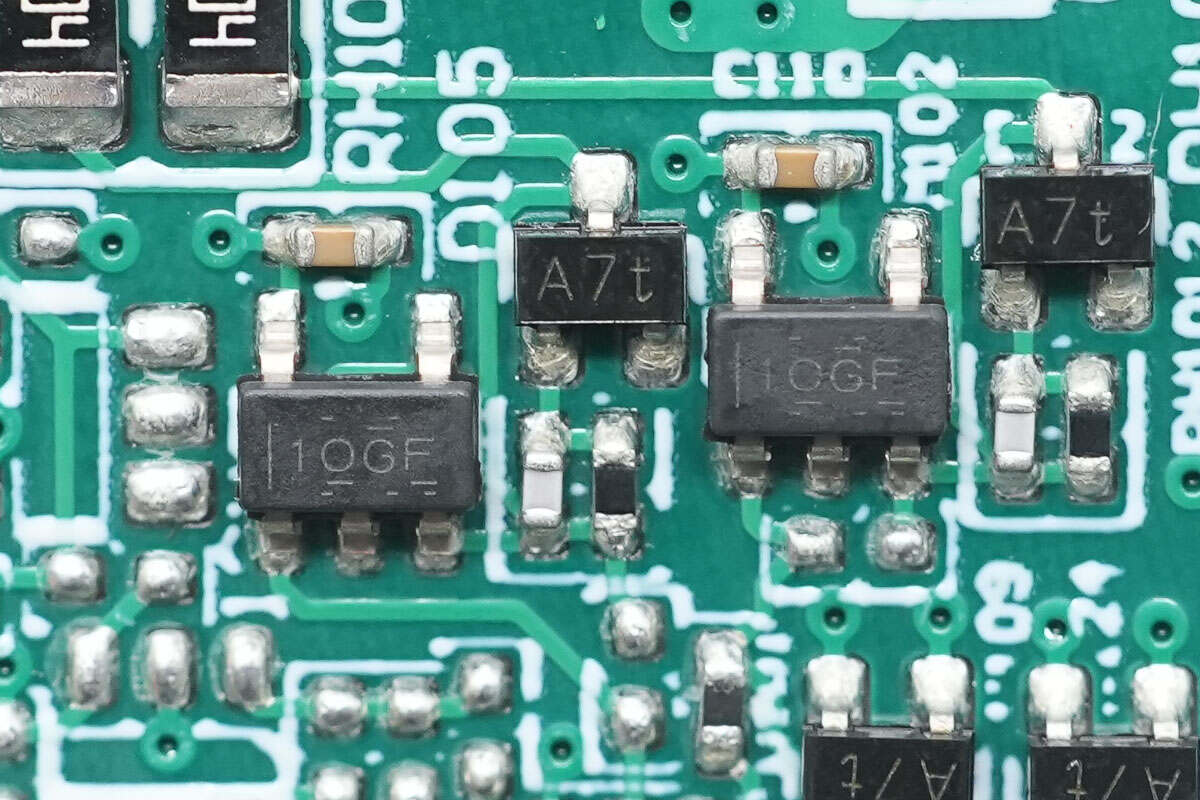
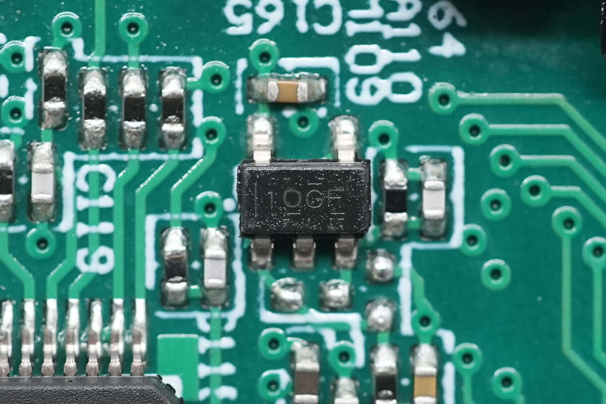
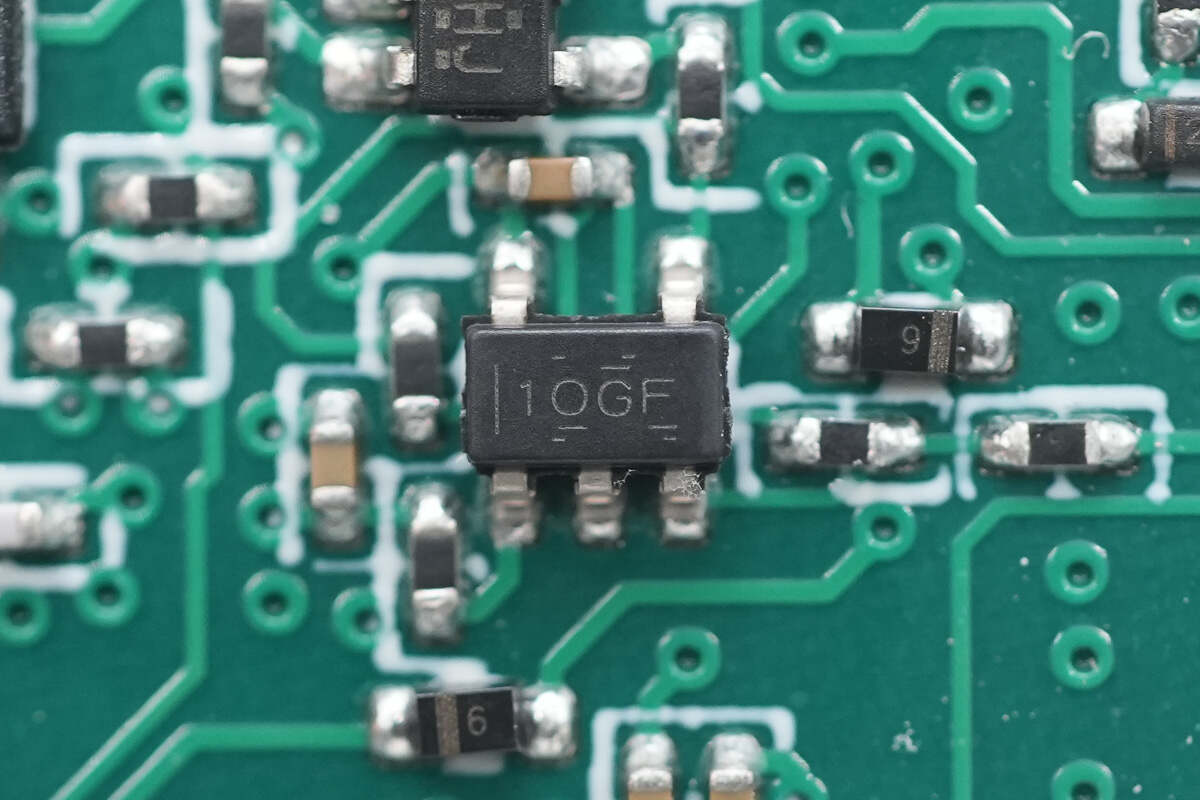
The operational amplifier chip is from TI, marked 1OGF, model TLV9001. It is a single-channel, rail-to-rail input and output op-amp, supporting a 1.85–5.5 V operating voltage, and comes in a SOT-23 package.
Another operational amplifier has the same model.
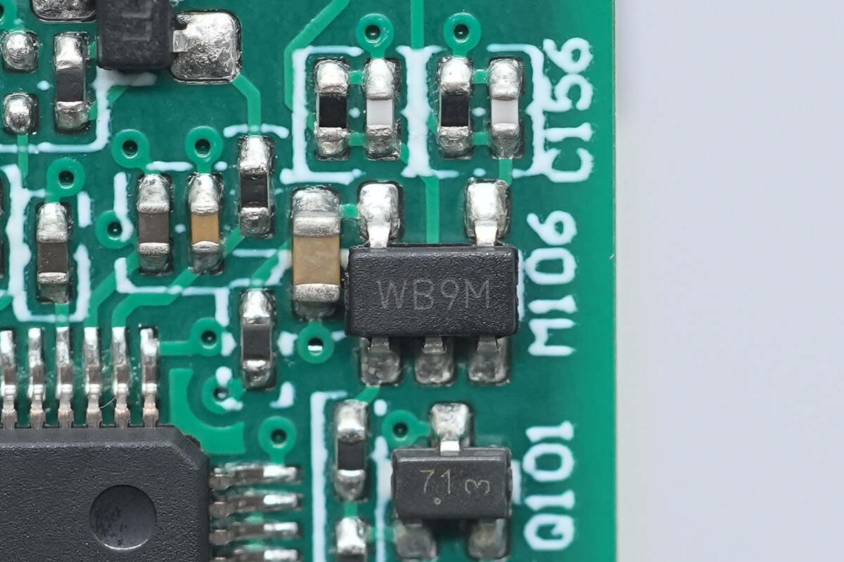
Close-up of the chip marked WB9M.
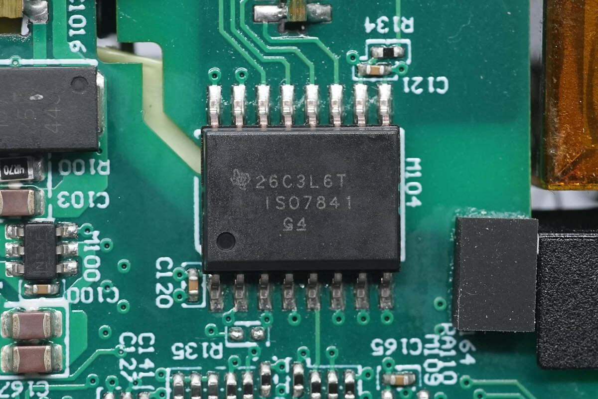
The digital isolation chip is from TI, model ISO7841. It is an enhanced four-channel digital isolator, supporting a 100 Mbps data rate, and comes in a 16-pin SOIC (DW) package.
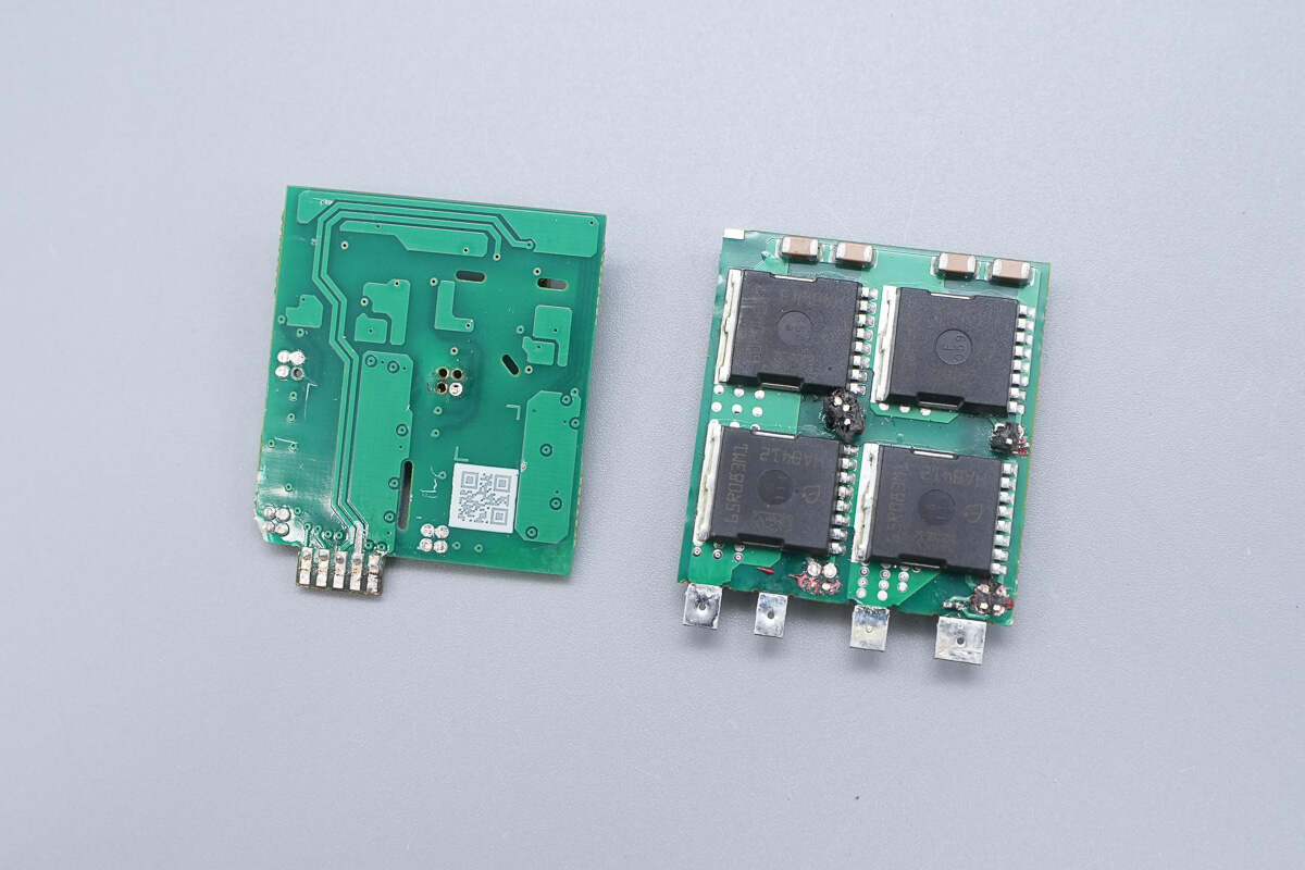
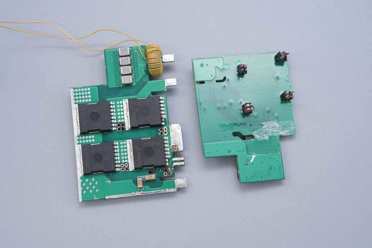
The two Totem-pole MOSFET PCBs have identical appearances and are each composed of two PCBs joined together by soldering.
One of the PCBs is equipped with an isolated power supply and an isolated driver.
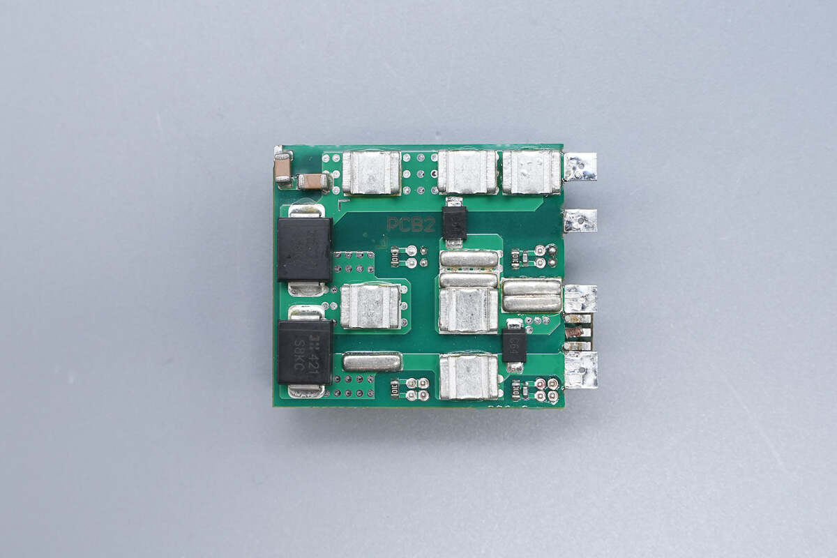
The other PCB is equipped with MOSFETs and diodes, with soldered copper plates added to enhance heat dissipation.
The two PCBs are connected via pin headers.
The front side of the driver PCB is soldered with two isolated drivers, two isolation transformers, and a power supply chip.
The back side of the PCB has no components.
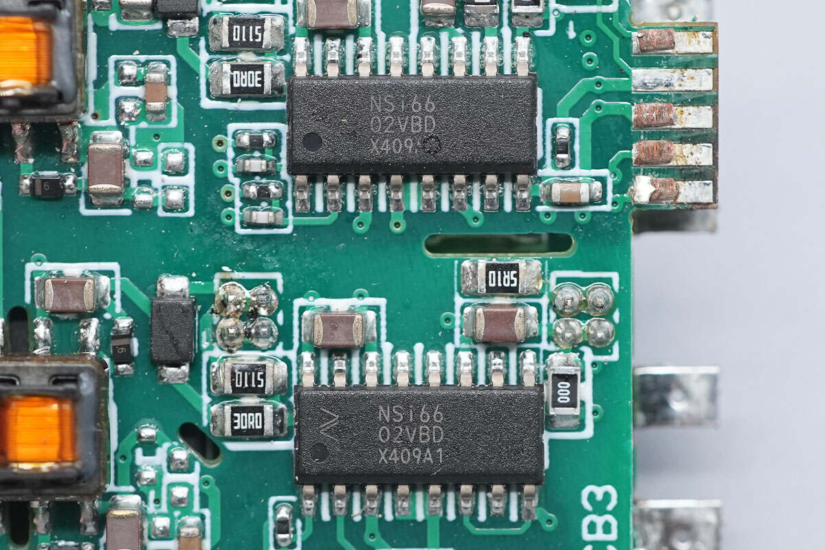
The isolated driver is from NOVOSENSE, model NSi6602V. It is the second-generation high-reliability isolated dual-channel gate driver from NOVOSENSE, featuring 6 A source current, 8 A sink current, a typical propagation delay of 25 ns, and comes in a SOP16 package.
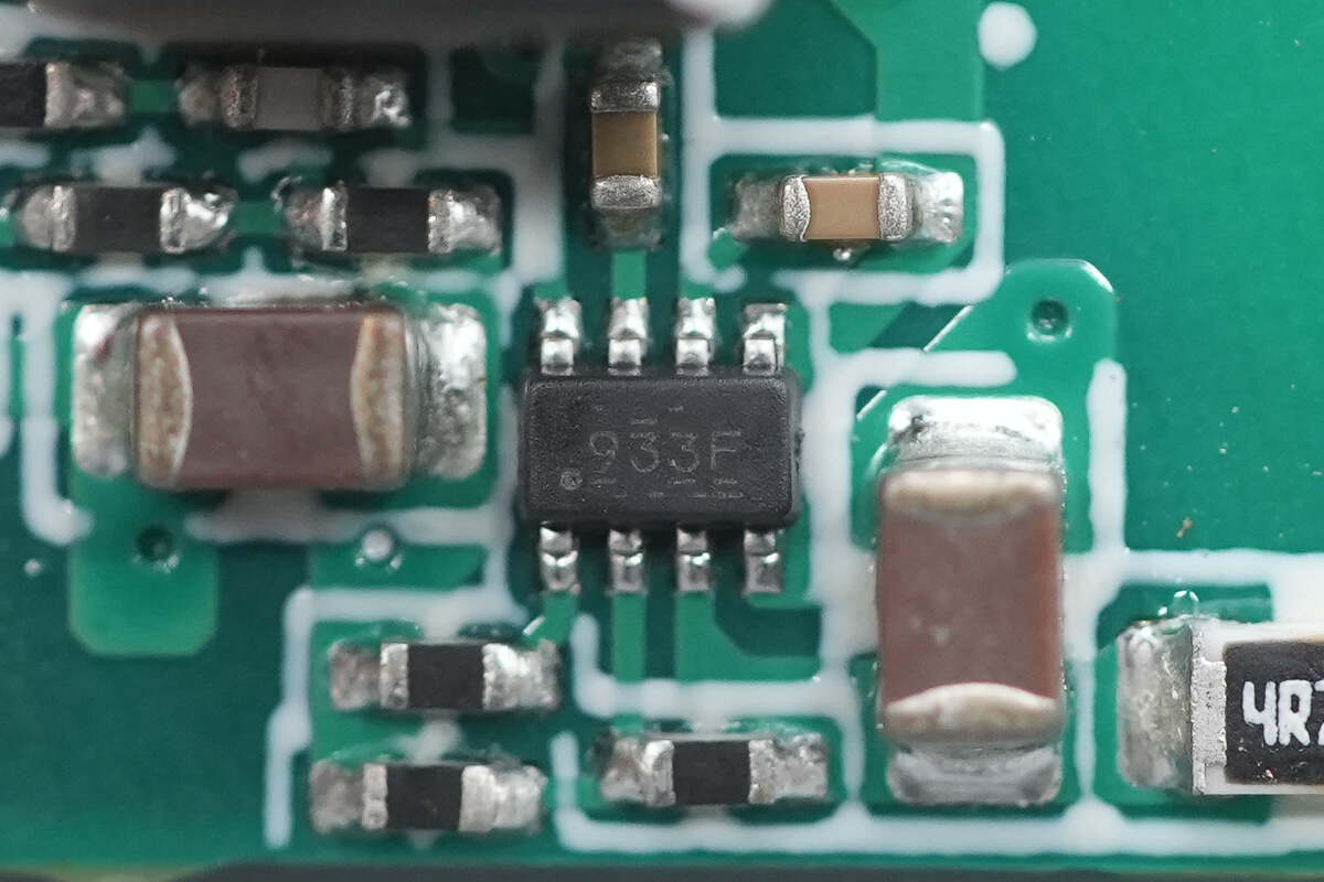
The synchronous buck chip is from TI, model TPS62933F. It is a synchronous step-down converter supporting an input voltage of 3.8–30 V and an output voltage range of 0.8–22 V. The chip integrates internal MOSFETs, supports a continuous output current of 3 A, and comes in a SOT583 package.
Close-up of the isolation transformers.
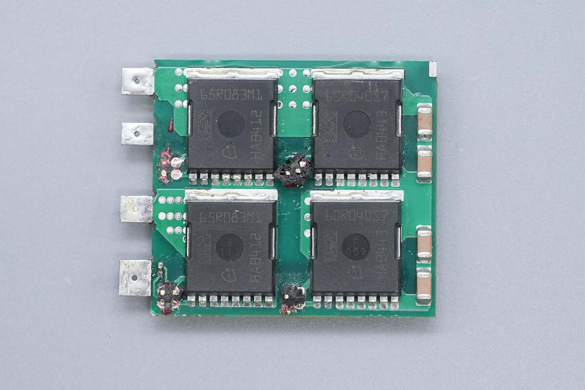
This PCB has four PFC MOSFETs.
The back side has copper strips to enhance current carrying capacity, soldered copper plates to increase heat dissipation area, and diodes for auxiliary rectification.
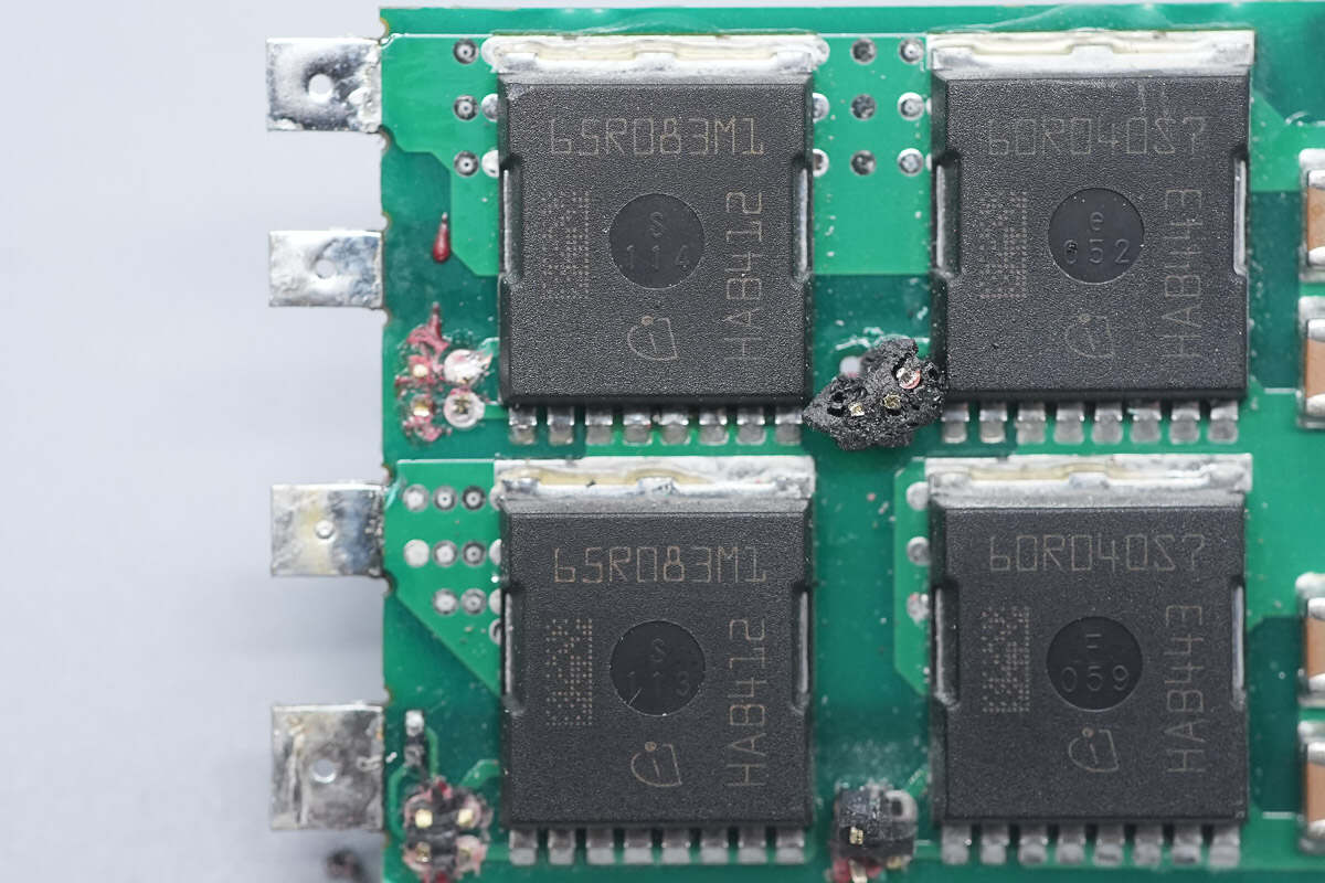
The two silicon carbide MOSFETs on the left are from Infineon, marked 65R083M1, model IMT65R083M1H, with a voltage rating of 650 V, an on-resistance of 83 mΩ, and come in an HSOF-8 package.
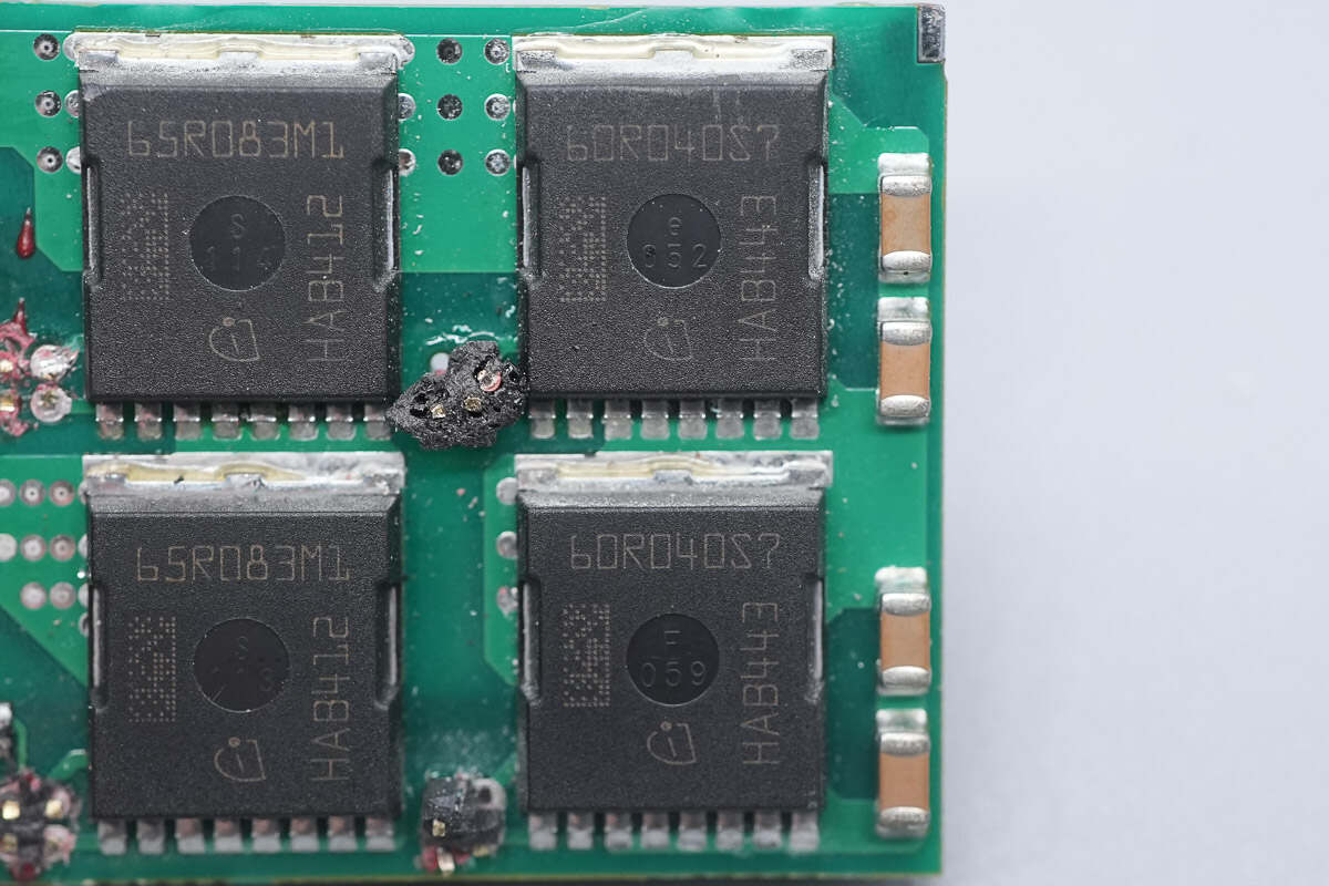
The two MOSFETs on the right are also from Infineon, marked 60R040S7, model IPT60R040S7. They are NMOS devices with a voltage rating of 650 V, an on-resistance of 45 mΩ, and come in an HSOF-8 package.
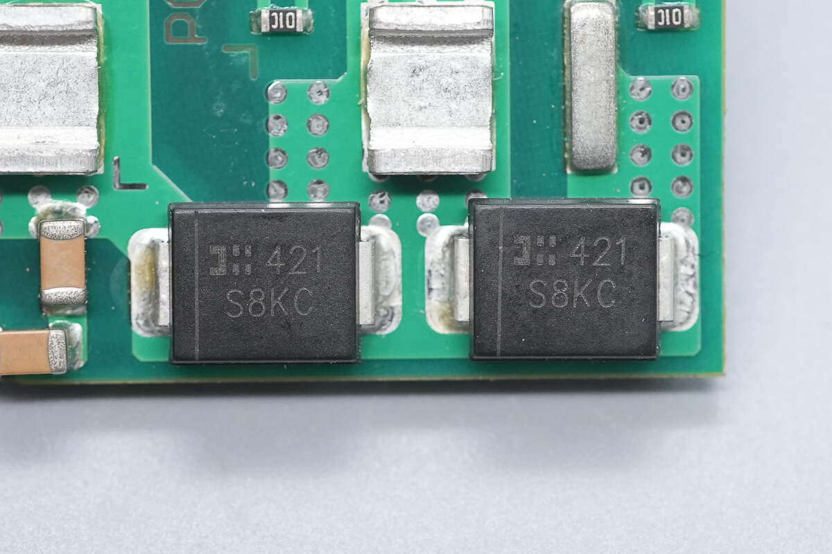
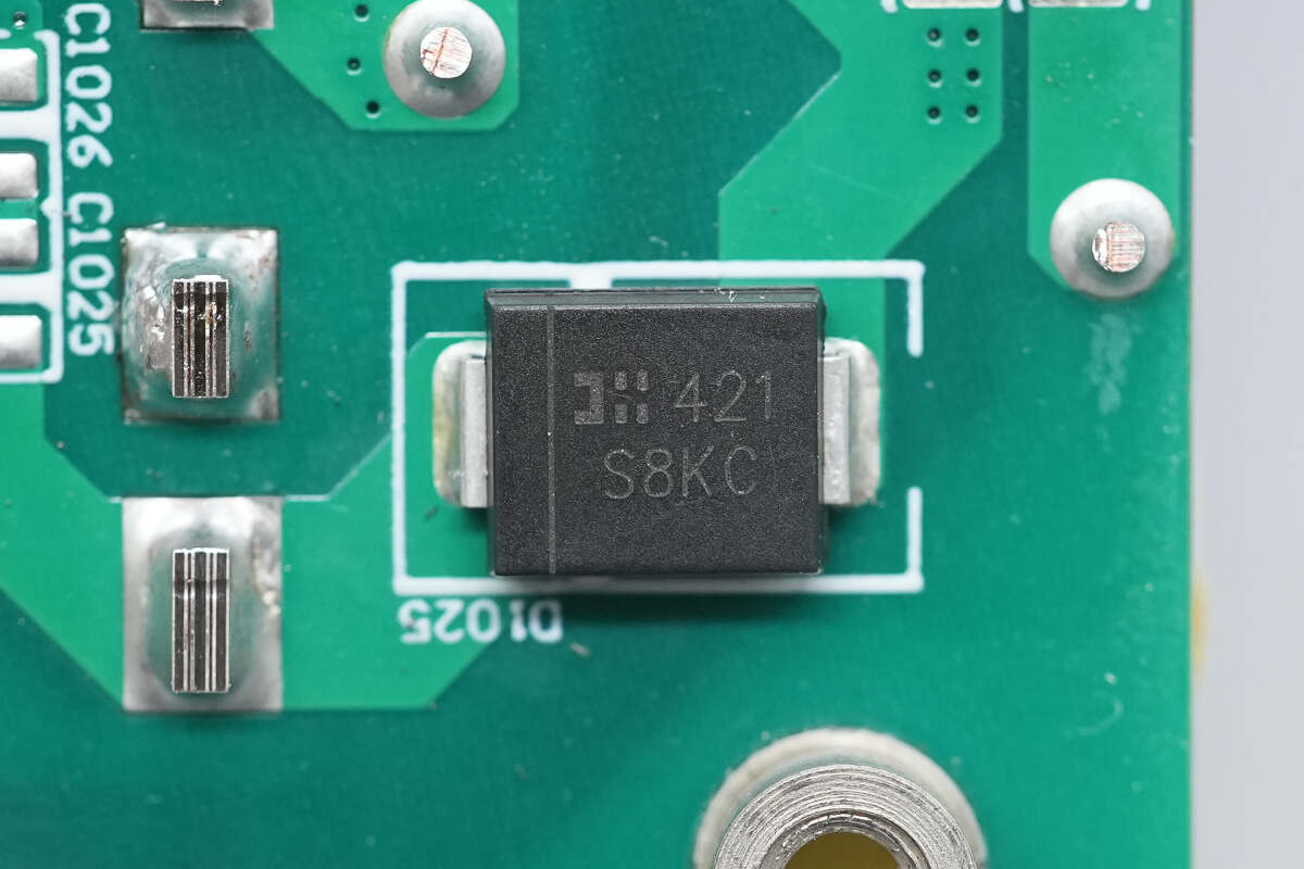
The two diodes are from DIODES, model S8KC, rated at 800 V, 8 A, and come in an SMC package.
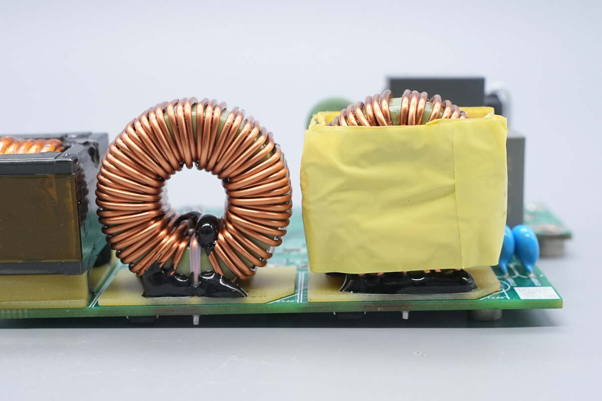
The PFC boost inductor is wound with enameled wire, with a Bakelite insulating board at the bottom and secured with adhesive.
The back side of the PCBA module has two diodes of the same model.
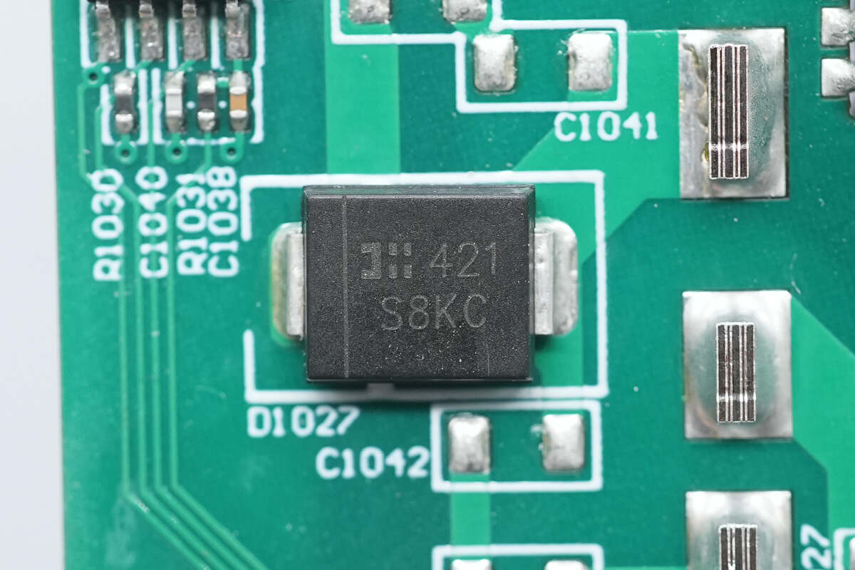
Close-up of the other diode.
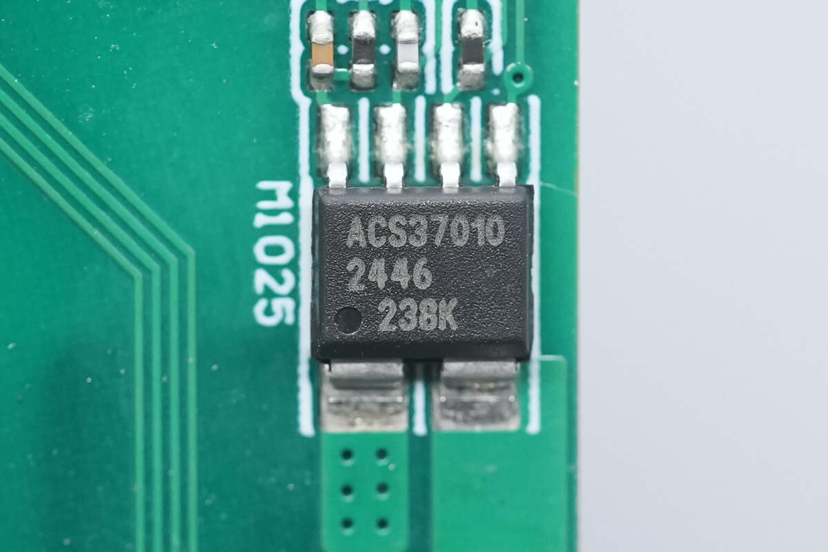
The current-sensing chip is from ALLERGO, model ACS37010. It features a 450 kHz bandwidth and high-precision current measurement, supports an operating temperature range of -40 °C to 150 °C, and comes in a SOIC-6 package.
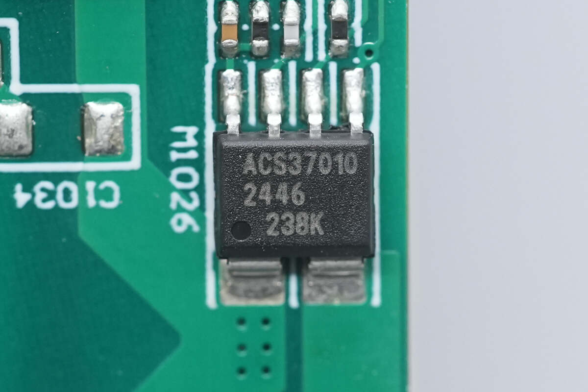
Another current-sensing chip has the same model and is used to measure the currents of the two Totem-pole PFC inductors.
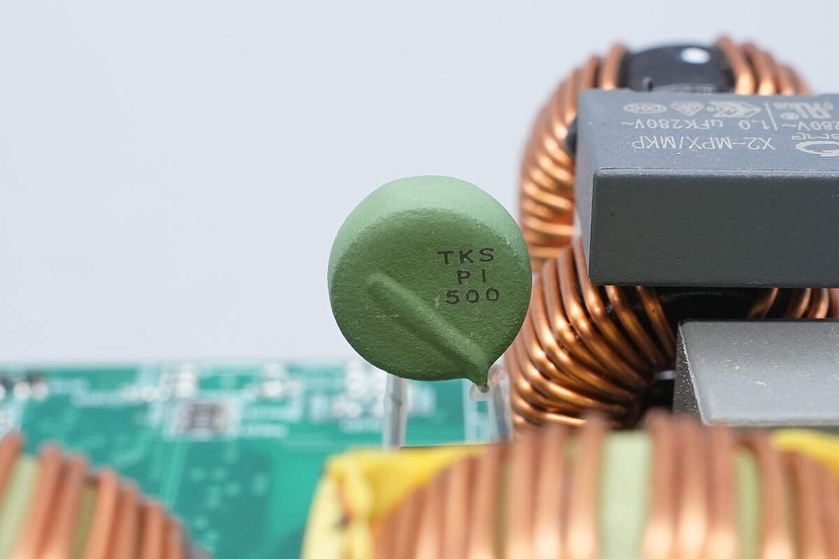
The thermistor is from Thinking, model TKS PI 500, used to suppress inrush current during power-on.
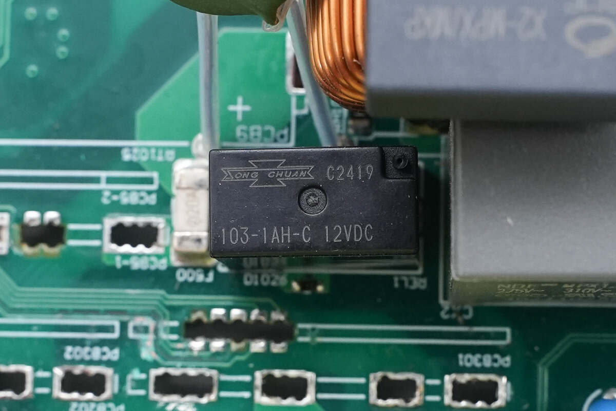
The relay is from SongChuan, model 103-1AH-C, with a single normally open contact and a 12 V coil voltage.
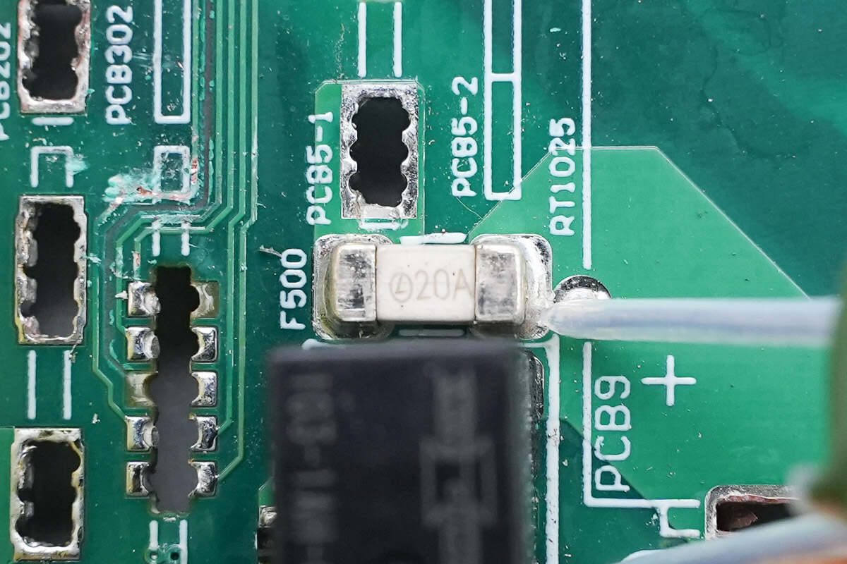
The SMD fuse is used for LLC-level overcurrent protection, with a rating of 20 A.
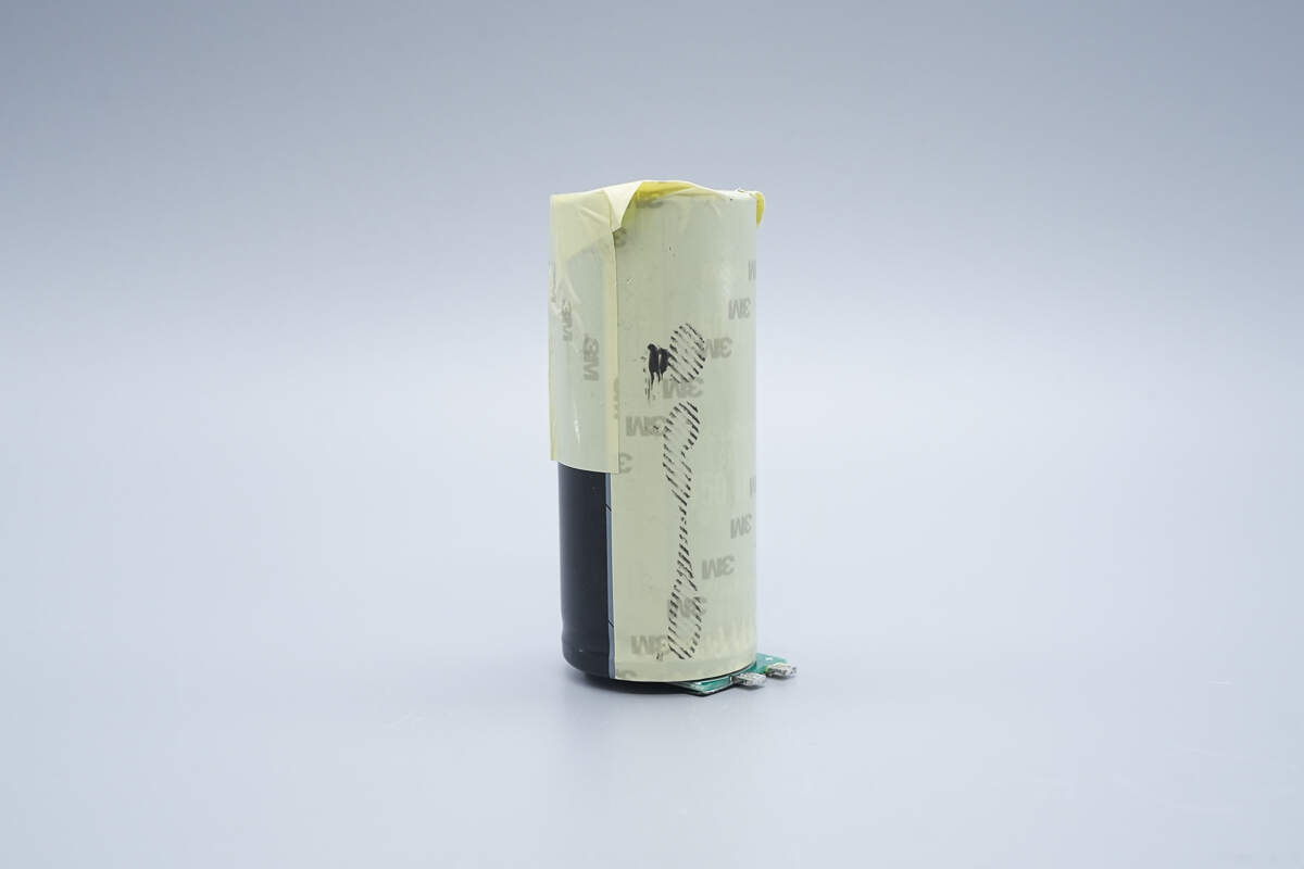
The high-voltage filter capacitor is insulated with wrapped tape.
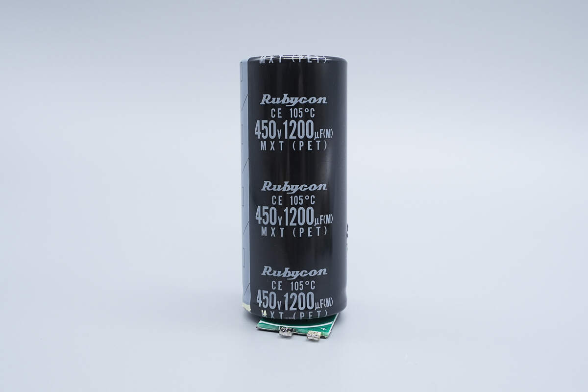
It is from Rubycon, part of the MXT series of ultra-compact electrolytic capacitors, with a rating of 450 V, 1200 μF.
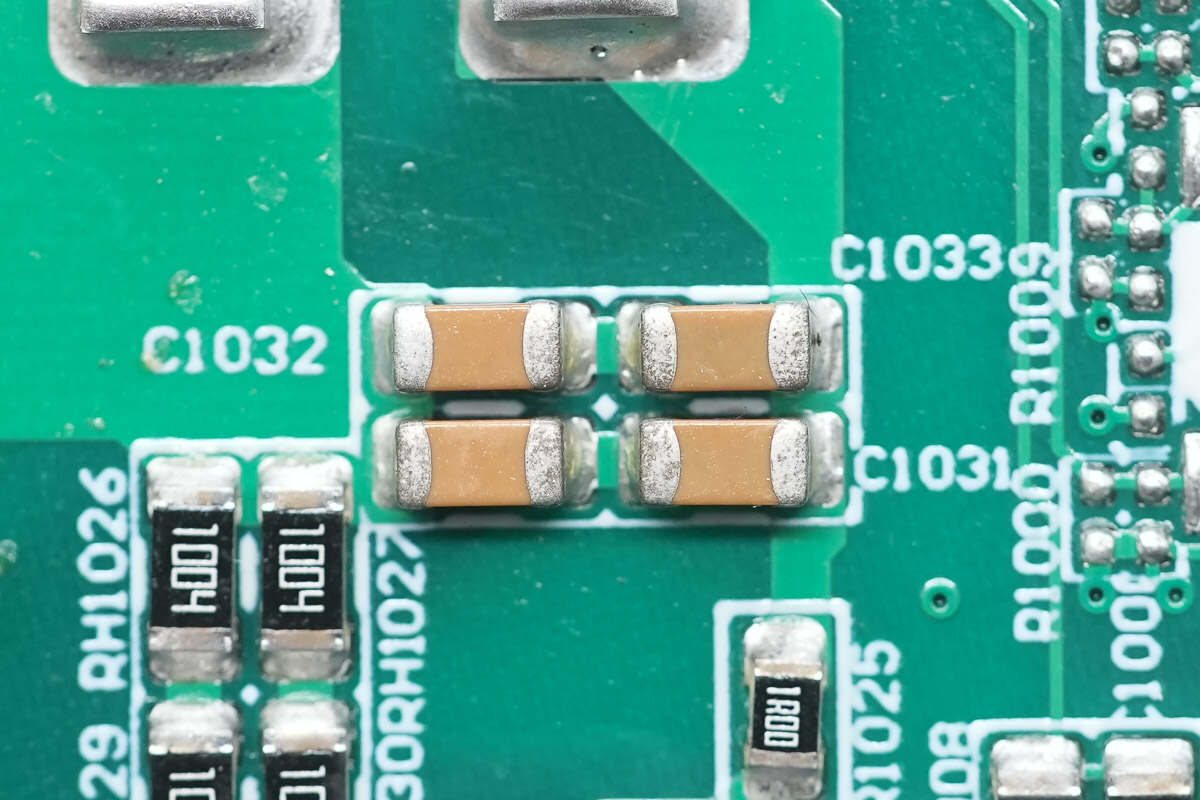
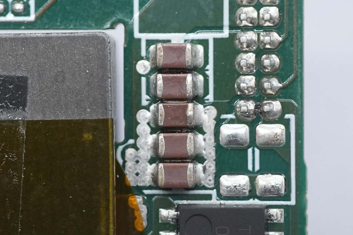
The MLCC capacitors are connected in parallel with the high-voltage filter capacitor.
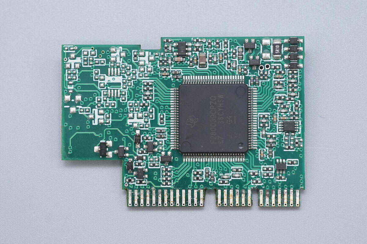
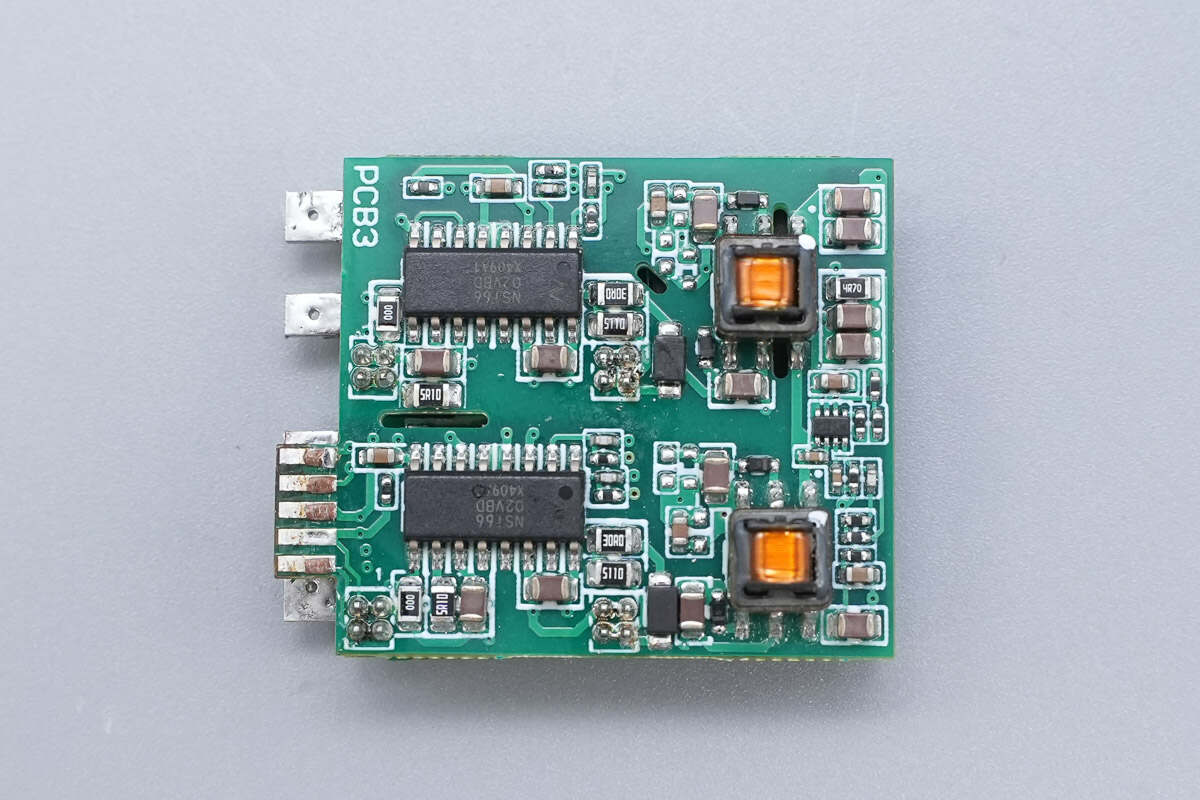
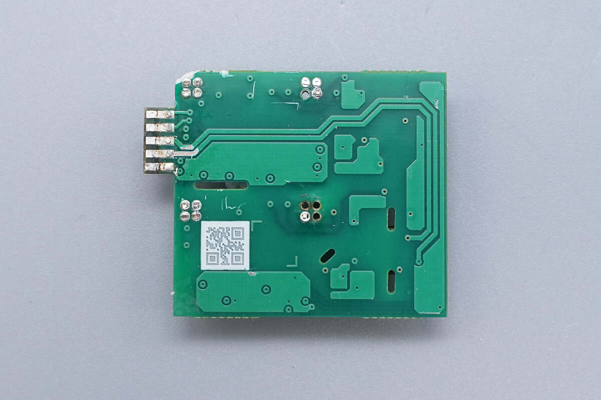
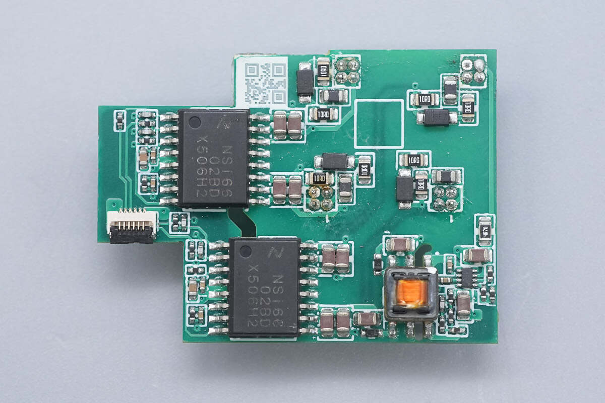
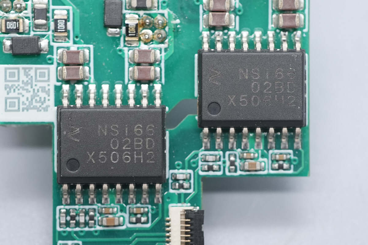
The LLC controller and op amp are located on the front of the LLC control PCB.
The back side houses the memory, op amp, and synchronous buck chip.
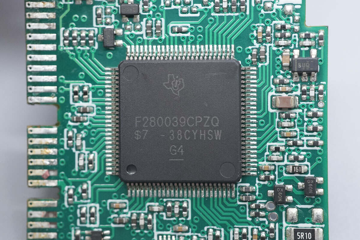
The LLC controller is from TI, model TMS320F280039C-Q1, the same model as the PFC controller.
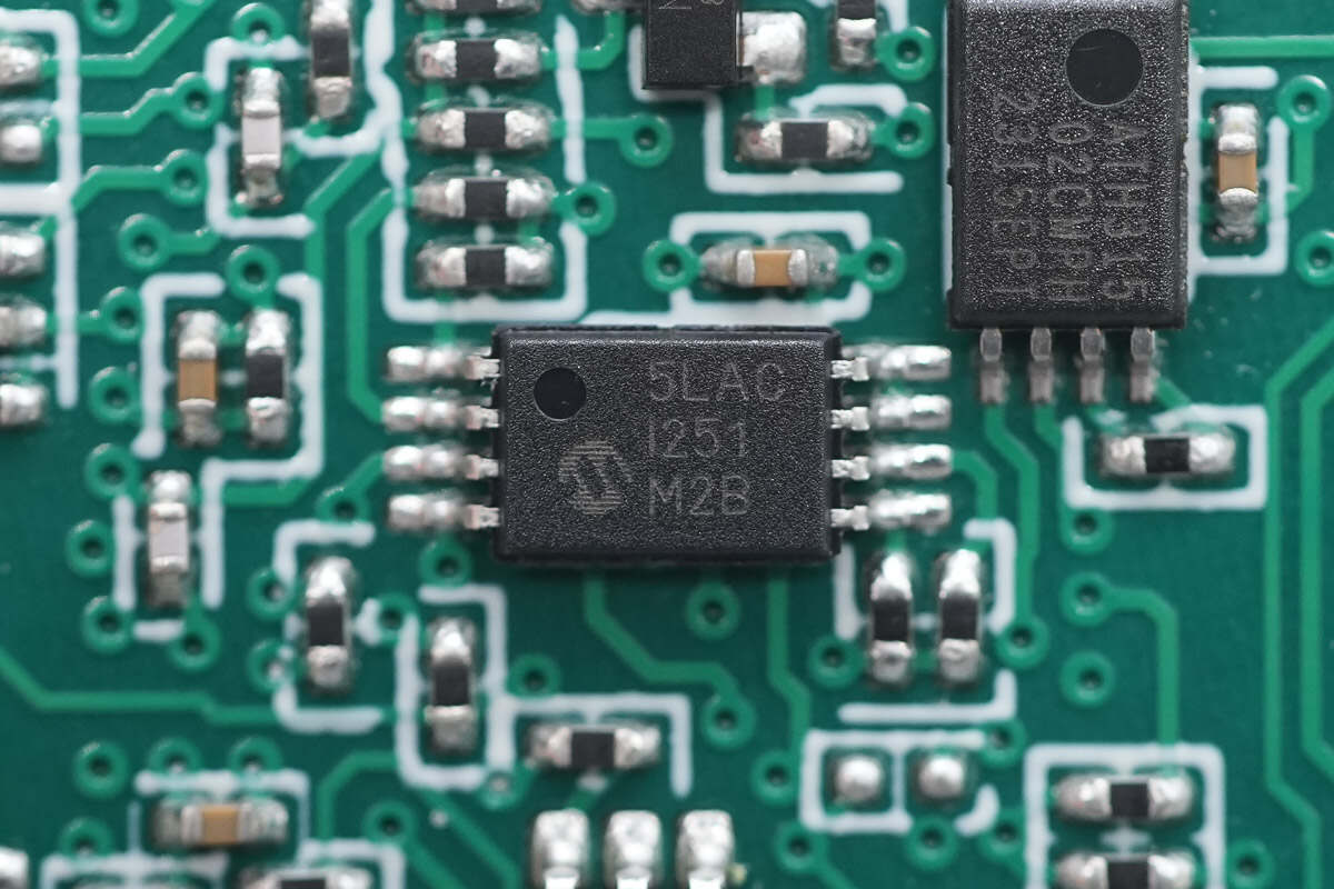
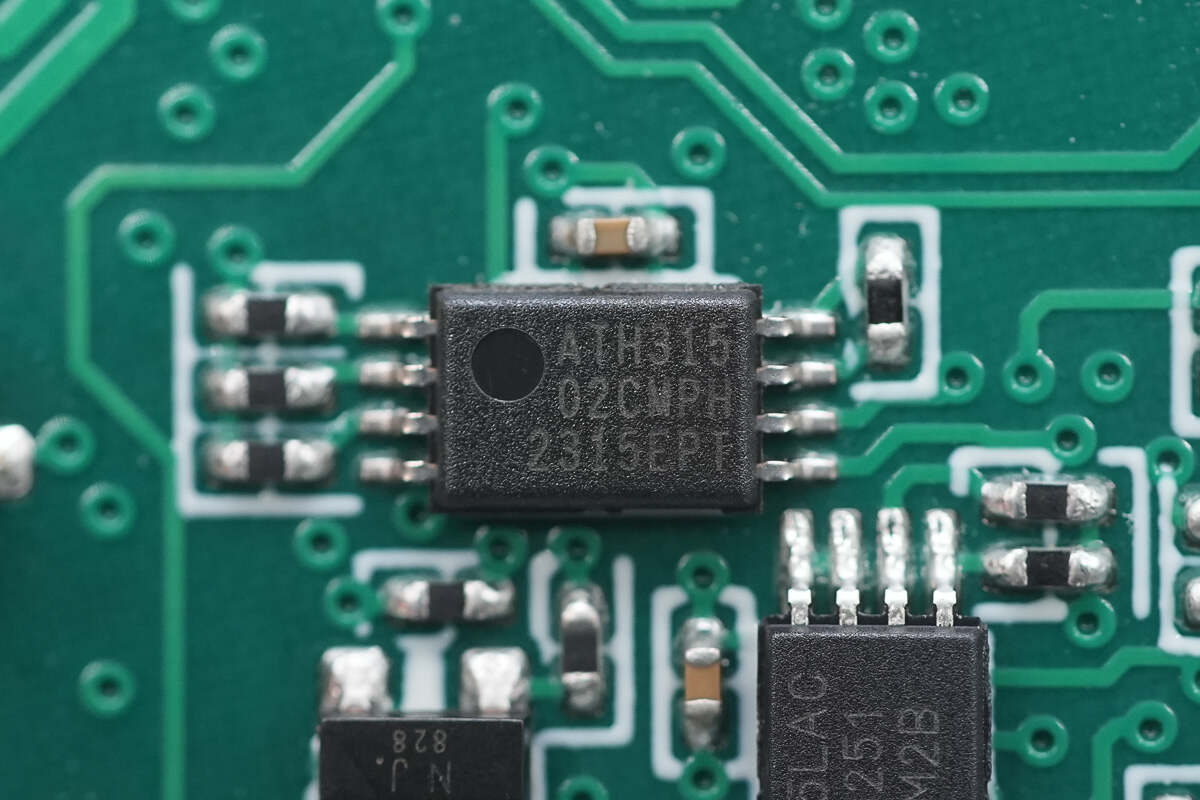
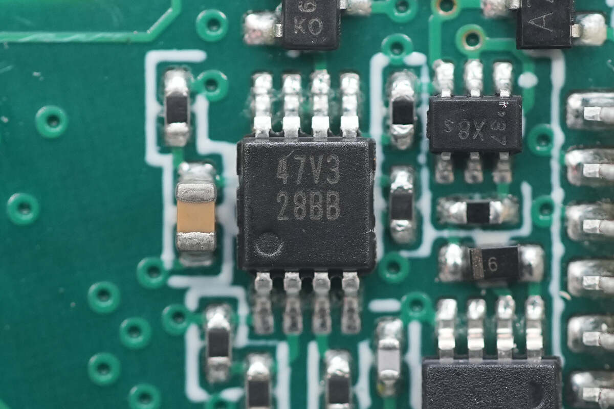
The memory is from Microchip, marked with 5LAC, model 25LC160C, with a capacity of 2KB, supports an operating voltage range of 2.5-5.5V, and uses a TSSOP package.
The memory is from Microchip, marked with 02C, model AT24C02C, with a capacity of 256B, supports an operating voltage range of 1.7-5.5V, and uses a TSSOP package.
The synchronous buck chip uses the TI TPS560430X3F.
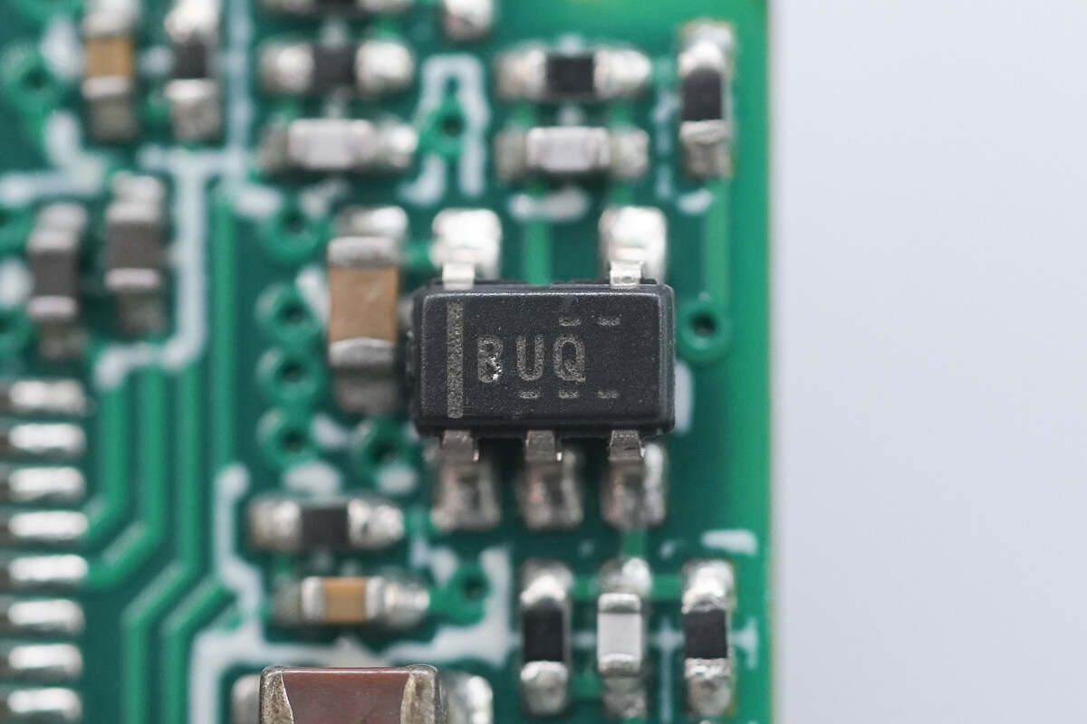
The op amp is from TI, marked with BUQ, model OPA376, which is a precision low quiescent current op amp that supports rail-to-rail input and output and uses a SOT-23 package.
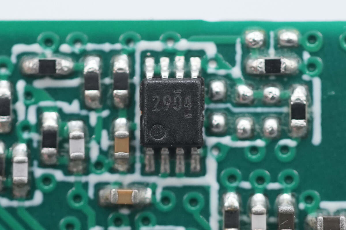
Close-up of the op amp marked with 2904.
The op amp is from TI, marked with 28BB, model LM2904B, an industry-standard dual operational amplifier in a VSSOP8 package.
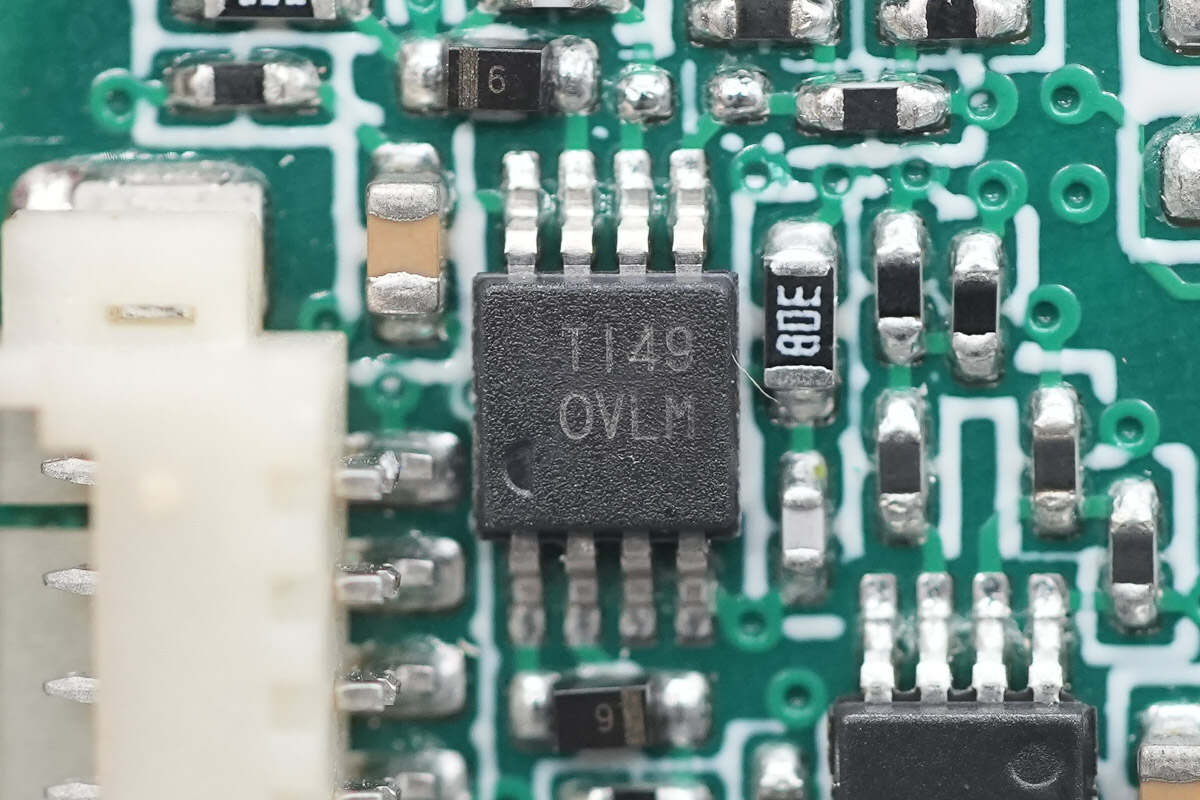
The op amp is from TI, marked with OVLM, model OPA2192, which is a low offset voltage, low input bias current, rail-to-rail input and output precision operational amplifier with excellent DC precision and AC performance, and is packaged in VSSOP8.
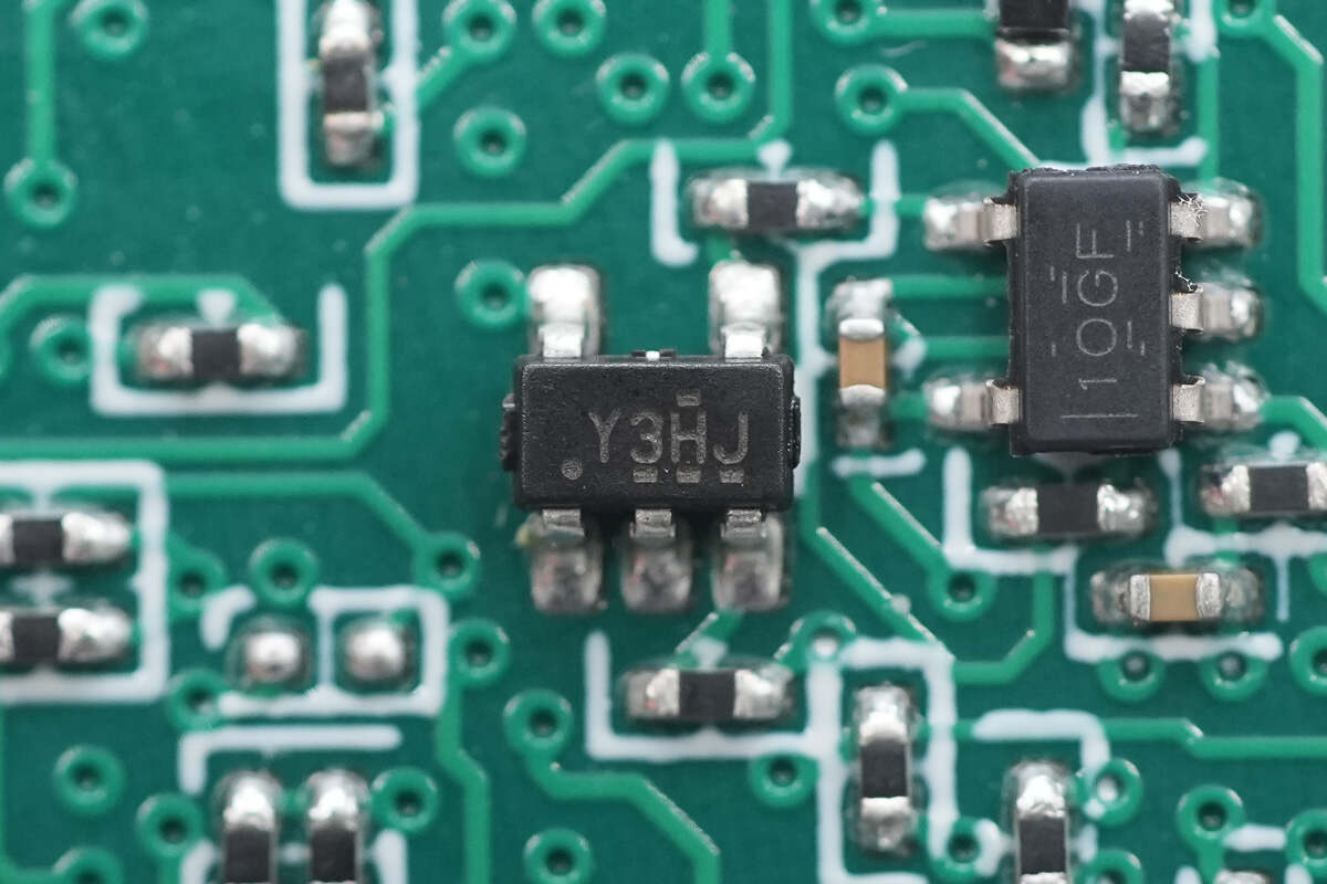
The voltage reference is from TI, marked with Y3HJ, model TLV431B, with a reference voltage of 1.24V, a tolerance of 0.5%, and is packaged in a SOT23-5.
The op amp is from TI, model TLV9001.
Close-up of the connectors of the current transformer and indicator light.
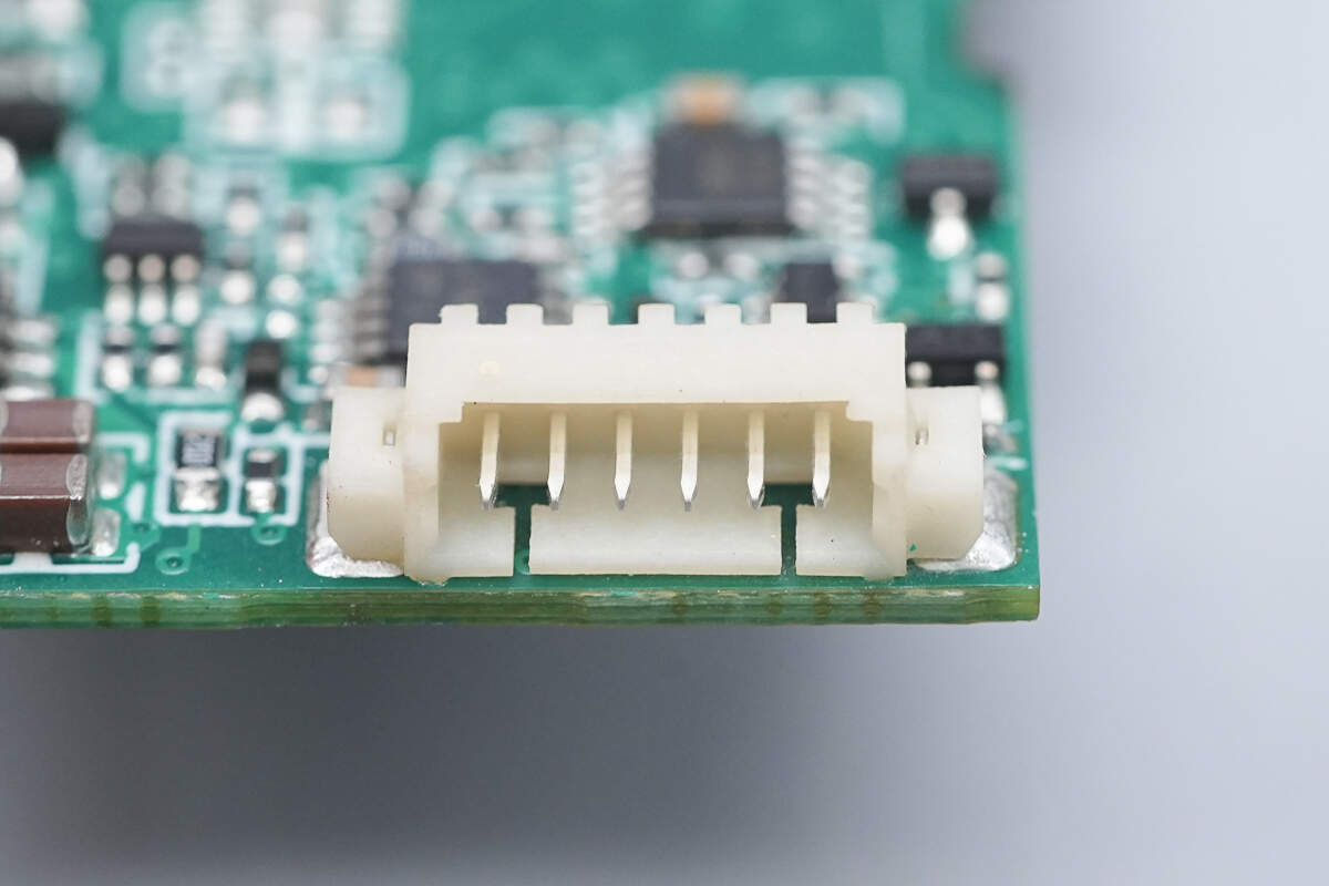
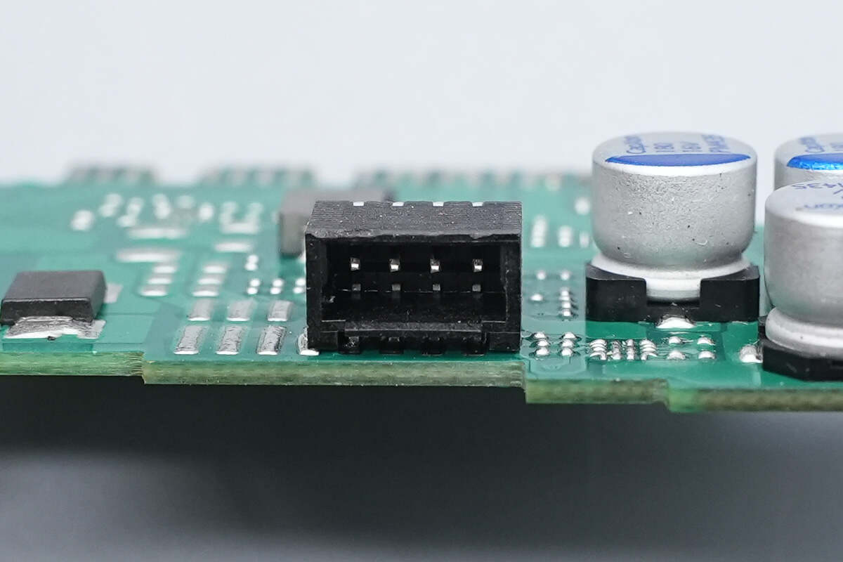
Close-up of the reserved connector.
Close-up of the connector for the PCB of the LLC MOSFETs.
The PCB of LLC MOSEFTs consists of two PCBs.
The copper sheets on the back are used to enhance heat dissipation.
Separate the two PCBs, which are connected via pin headers.
There are isolation drivers, an isolation transformer, and a power chip on the front of the driver PCB.
There are no components on the back.
The drivers for the LLC MOSFETs are from NOVOSENSE, model NSi6602BD. The chip has a built-in isolated dual-channel gate driver with 4A source current and 6A sink current capability, and is packaged in a SOW16 package.
The synchronous buck chip uses TI TPS62933F.
Close-up of the isolation transformer.
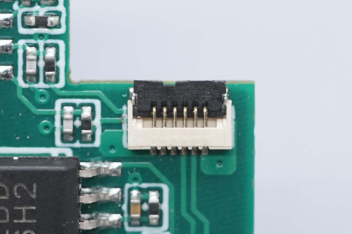
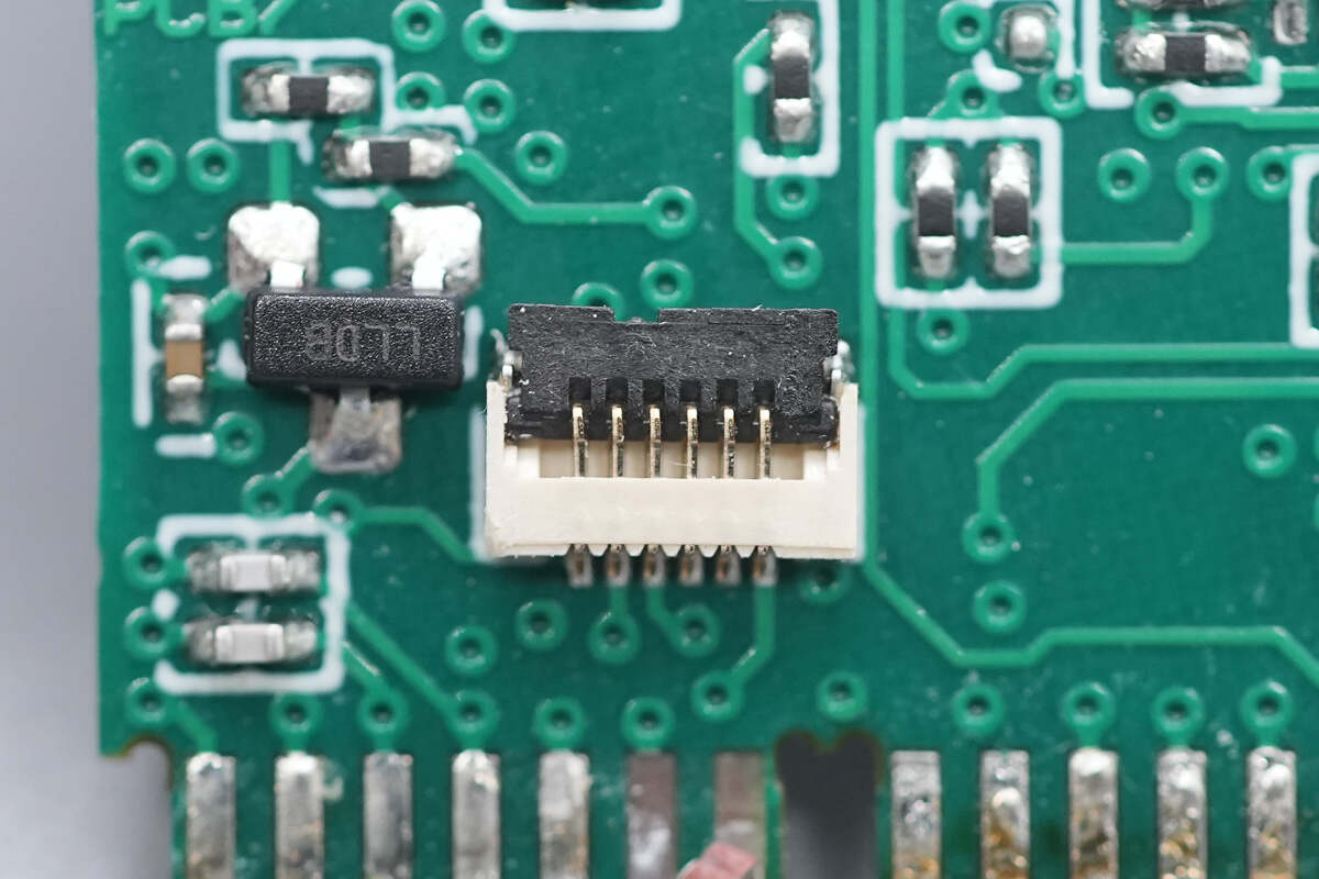
Close-up of the cable socket connected to the control PCB.
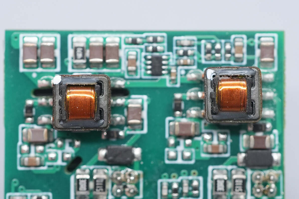
The front of this PCB has four LLC MOSFETs forming a full-bridge LLC, and the right side has resonant capacitors and a current transformer.
The copper sheets on the back enhance heat dissipation.
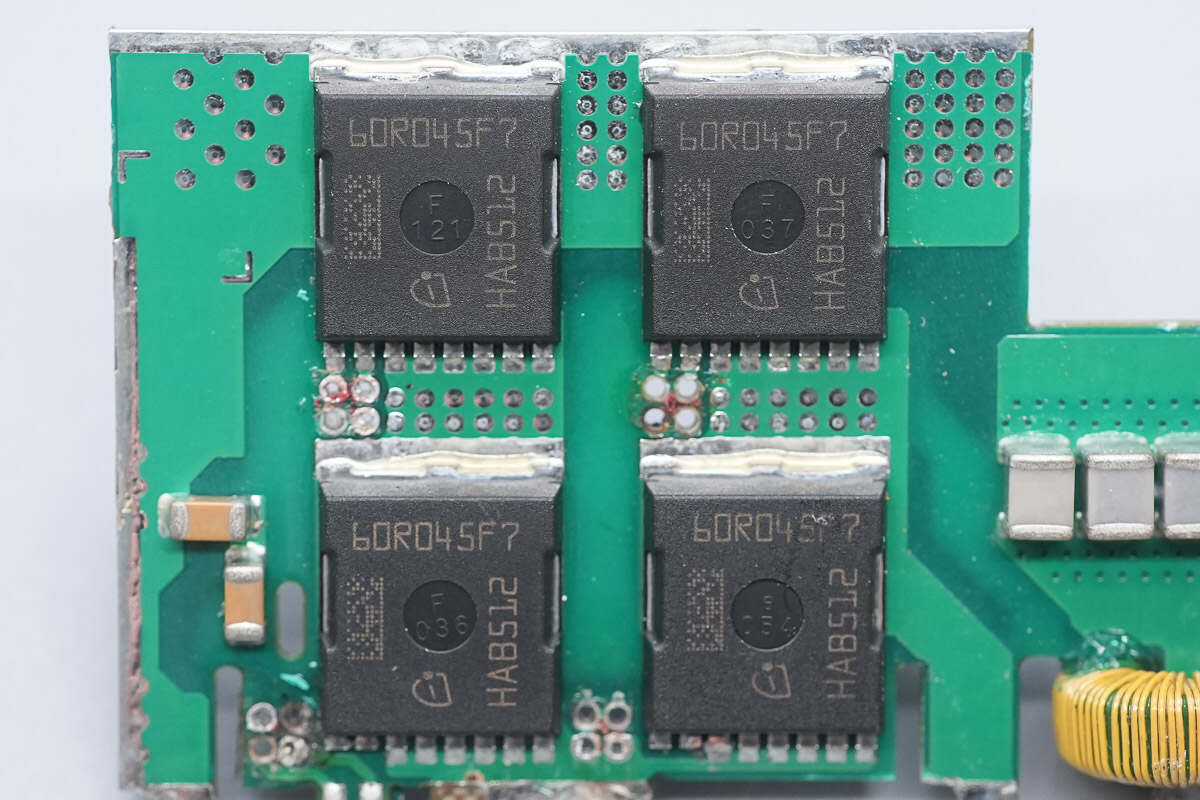
The LLC MOSFETs are from Infineon, marked with 60R045F7, model IPT60R045CFD7, NMOS, with a withstand voltage of 650V, a resistance of 45mΩ, and are packaged in an HSOF-8 package.

The NPO resonant capacitors are packaged in 1210.
There is also a resonant capacitor on the back.
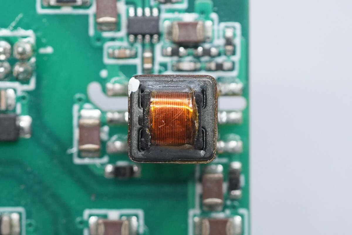
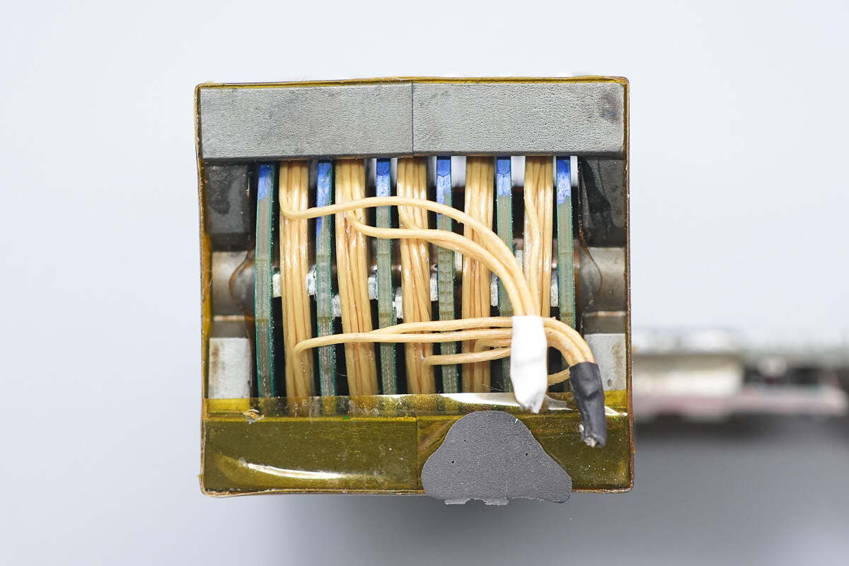
The current transformer is wound with multi-layer insulated wire.
The resonant inductor is wound with Litz wire.
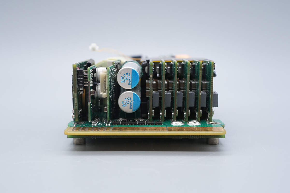
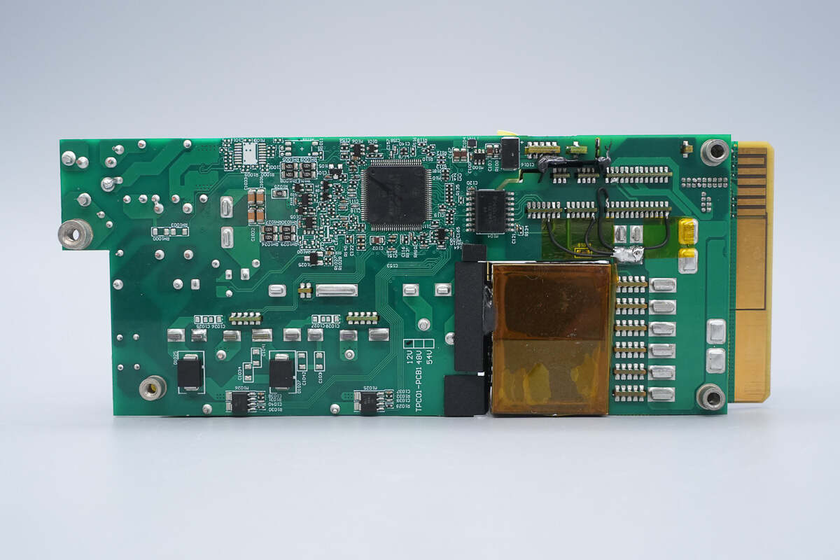
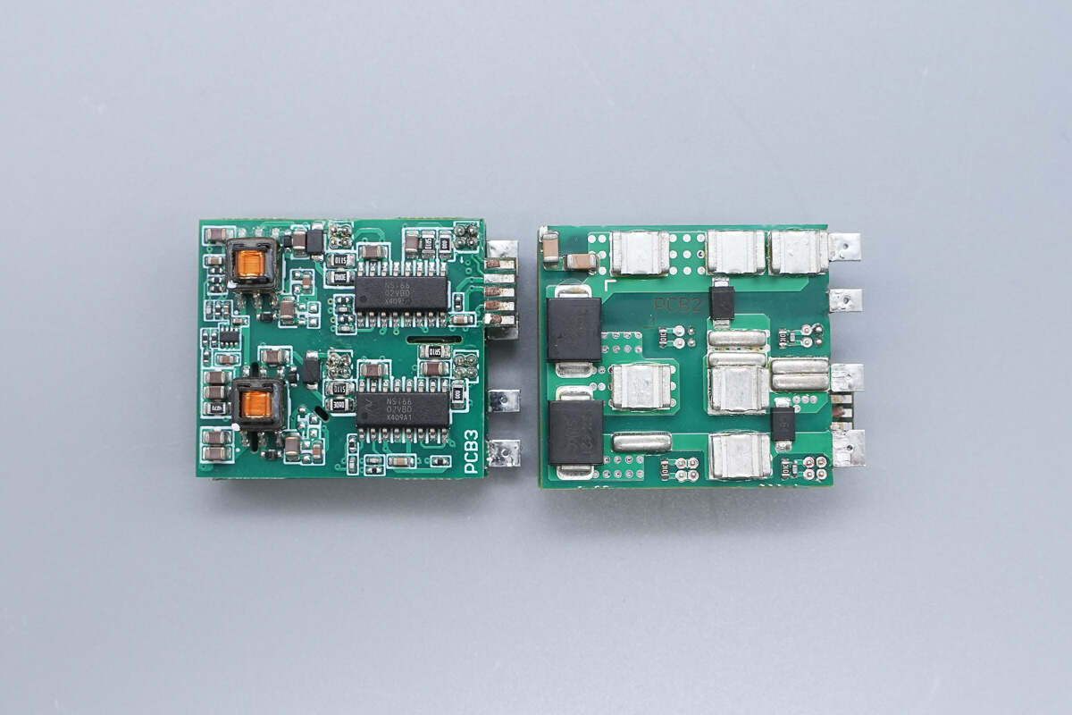
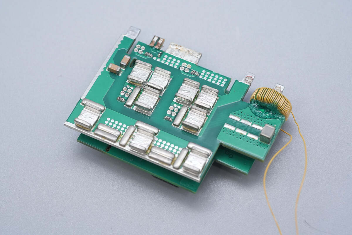
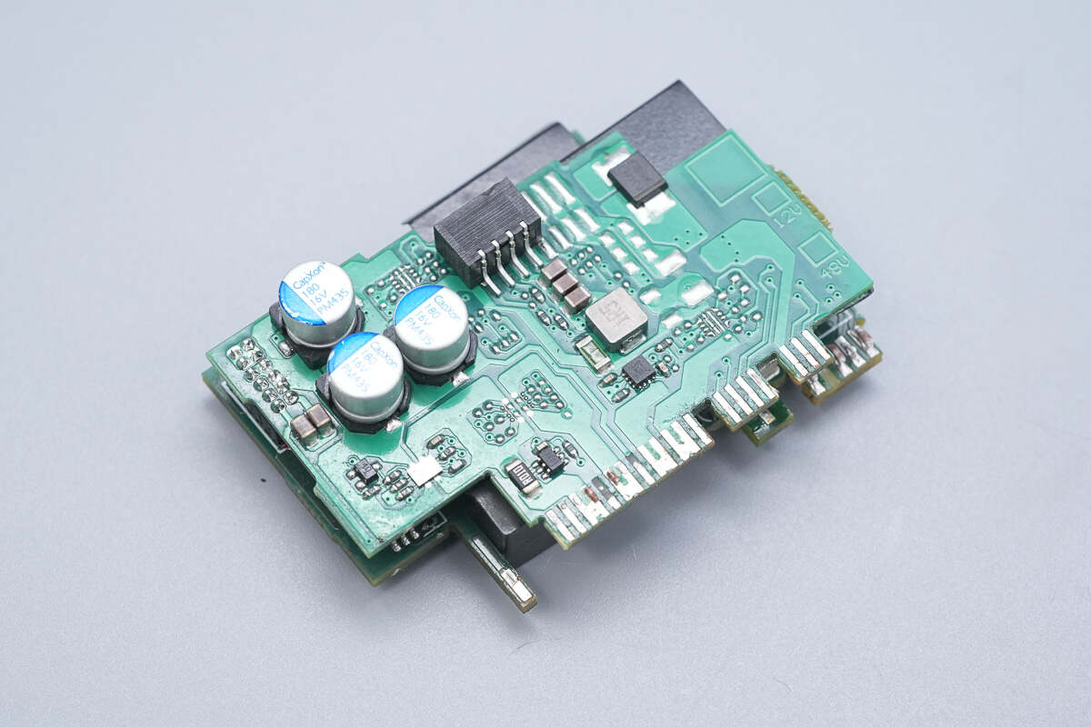
The output end is equipped with a standby power supply PCB, LLC control PCB, solid capacitors, and synchronous rectification PCB.
This is the synchronous rectification PCB.
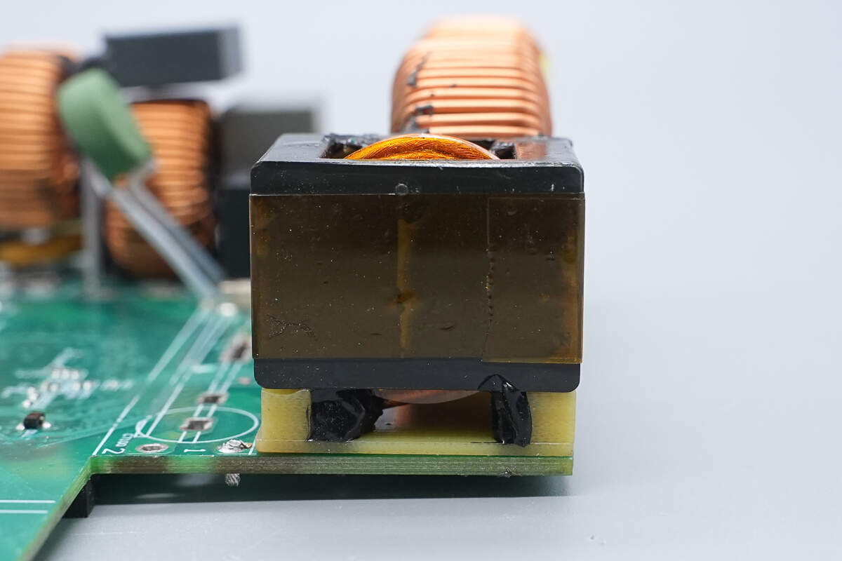
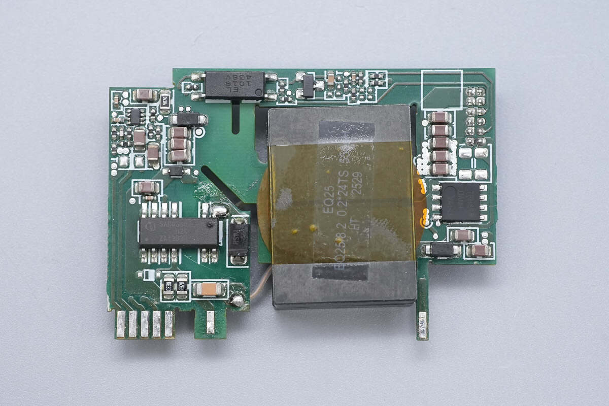
The primary winding of the transformer is wound with multi-layer insulated wire, while the secondary winding is manufactured using planar transformer technology.
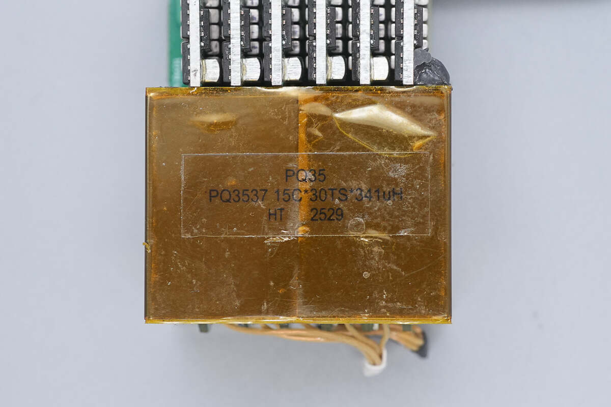
The transformer uses a PQ35 magnetic core and is insulated with high-temperature tape.
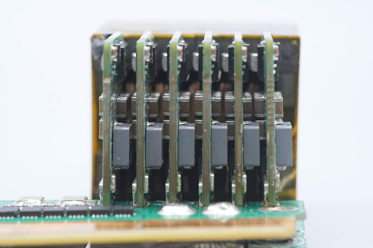
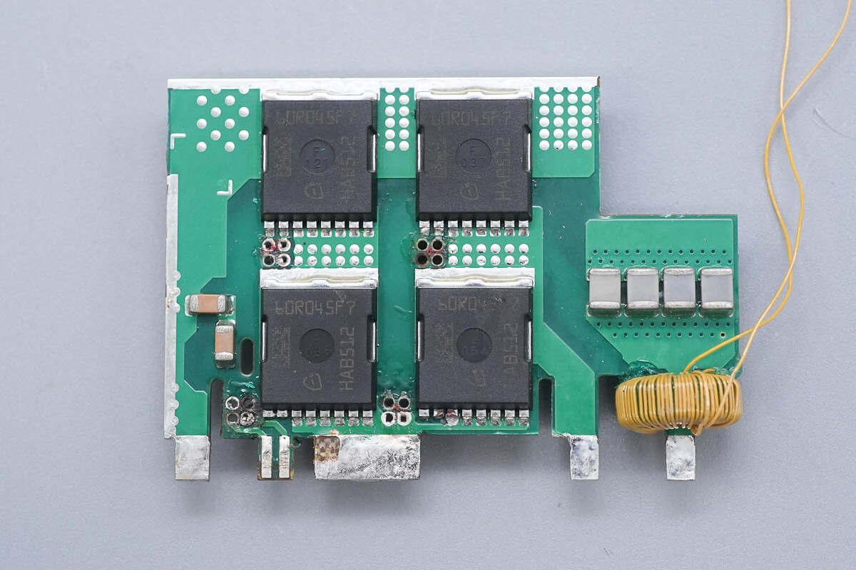
The output features six synchronous rectifier PCBs to evenly distribute heat.
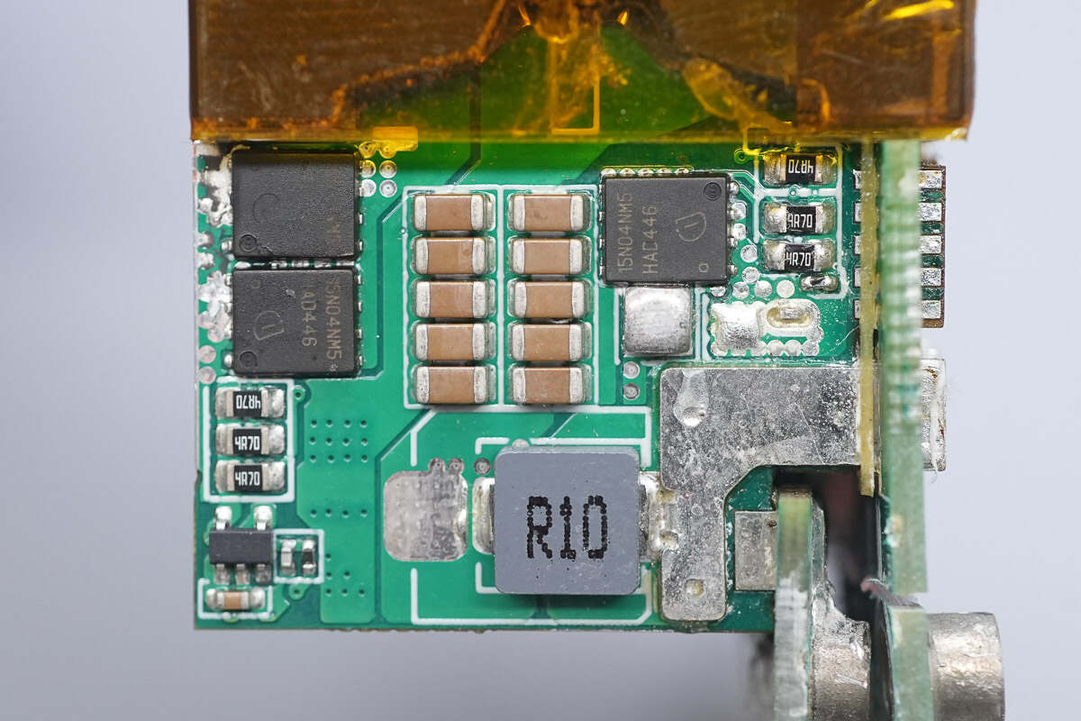
One side of the PCB is equipped with the synchronous rectifiers, driver, MLCC capacitors, and filter inductor.
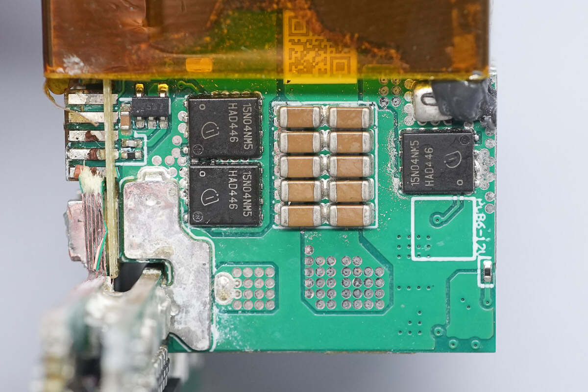
The other side is also equipped with synchronous rectifiers, a driver, and MLCC capacitors.
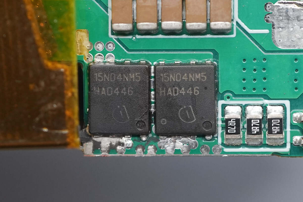
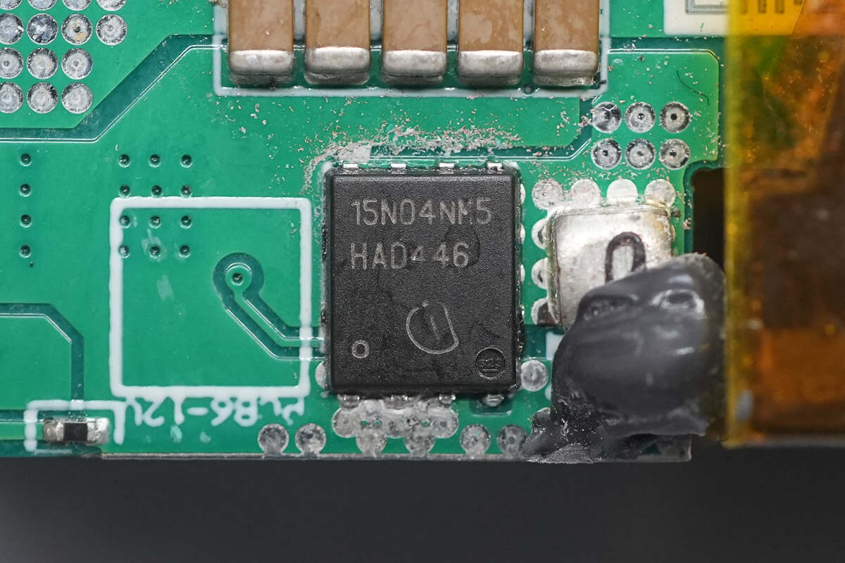
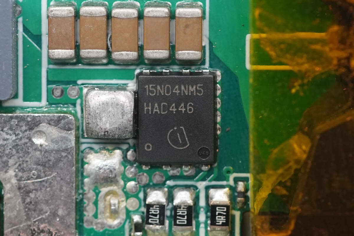
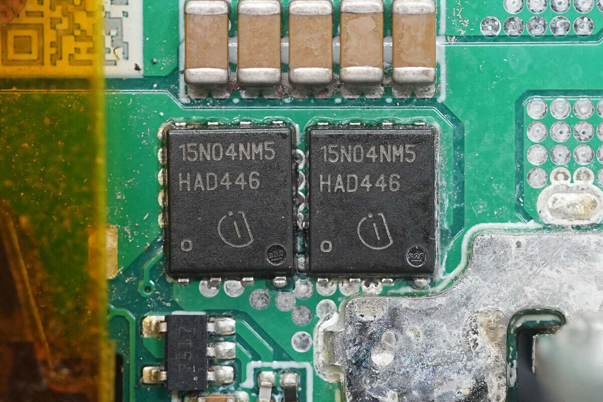
The synchronous rectifiers are from Infineon, model ISC015N04NM5, NMOS, with a withstand voltage of 40V, a resistance of 1.5mΩ, and are packaged in TDSON-8 FL.
There is also a synchronous rectifier of the same model on the other side.
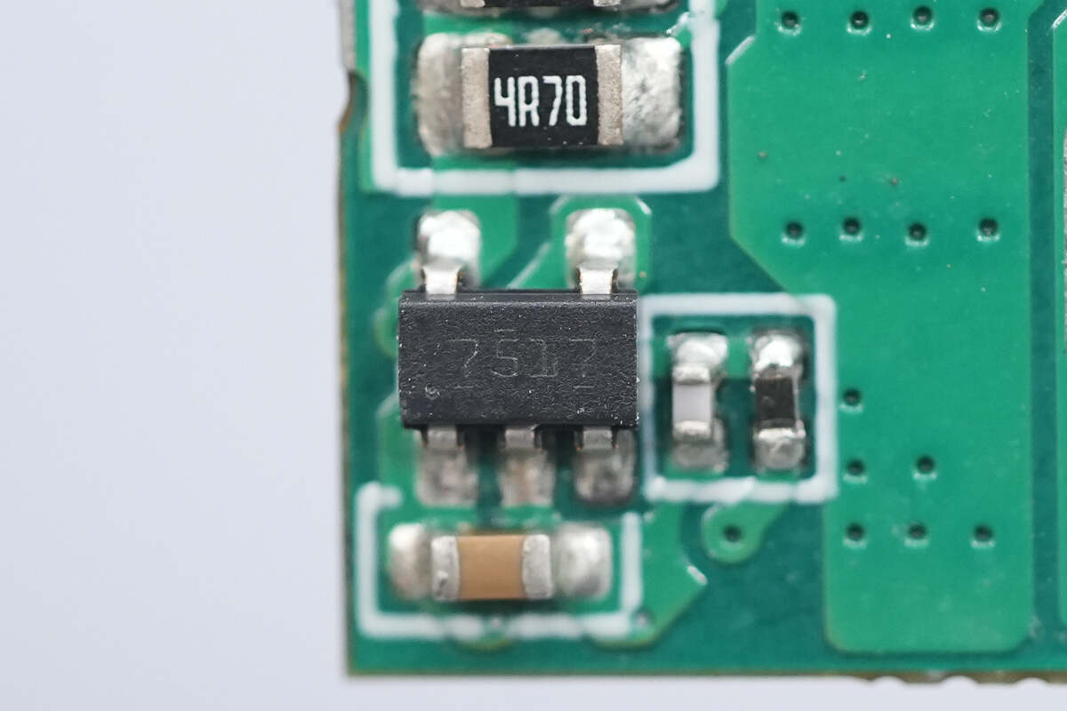
The driver is from TI, model UCC27517. It is a single-channel, high-speed low-side gate driver, supporting an operating voltage of 4.5–18 V. It features 4 A peak source and sink current, rail-to-rail drive capability, and comes in a SOT-23 package.
Another synchronous rectifier of the same model.
There are two synchronous rectifiers of the same model on the back.
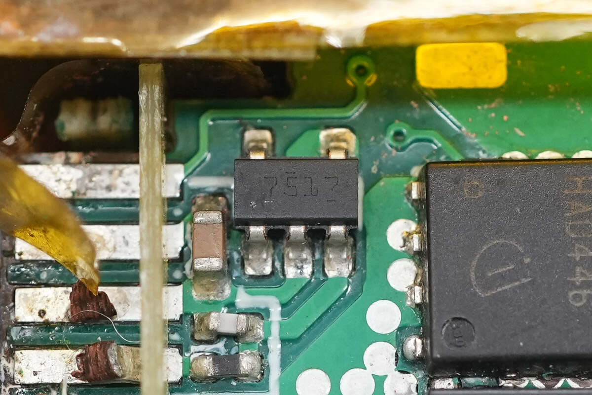
The driver uses TI UCC27517.
The MLCC capacitors are packaged in 1206, with 10 connected in parallel.
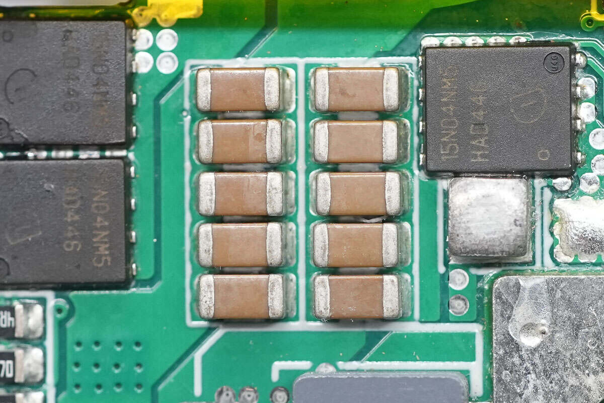
There are also 10 MLCC capacitors on the other side.
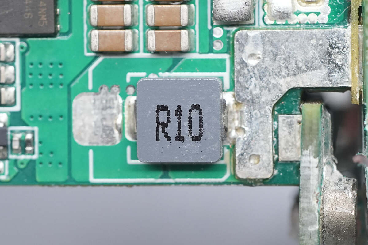
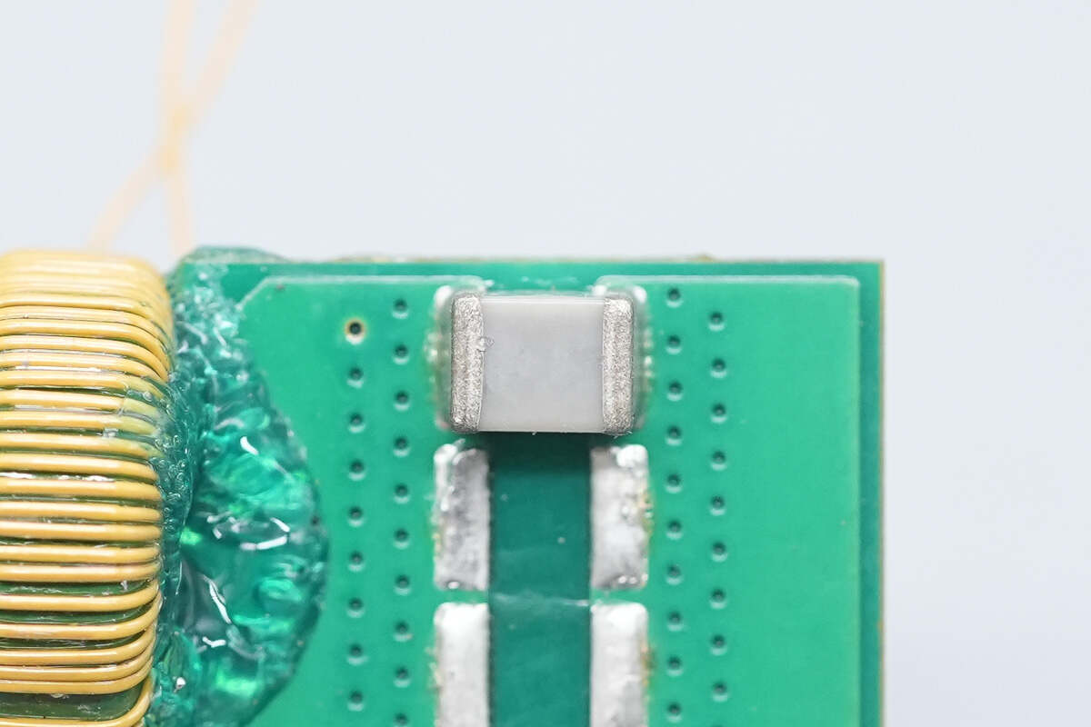
Close-up of the 0.1μH filter inductor.
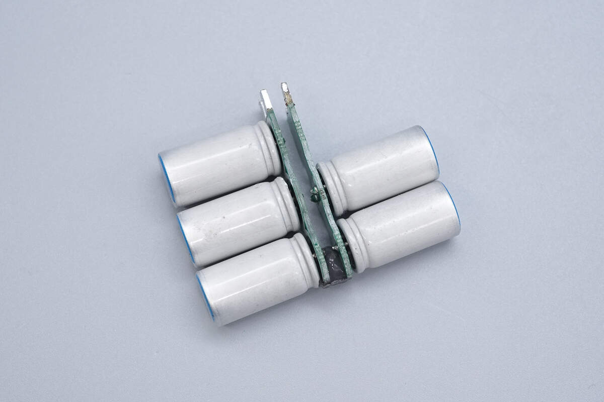
The capacitors for output filtering are soldered on vertical PCBs.
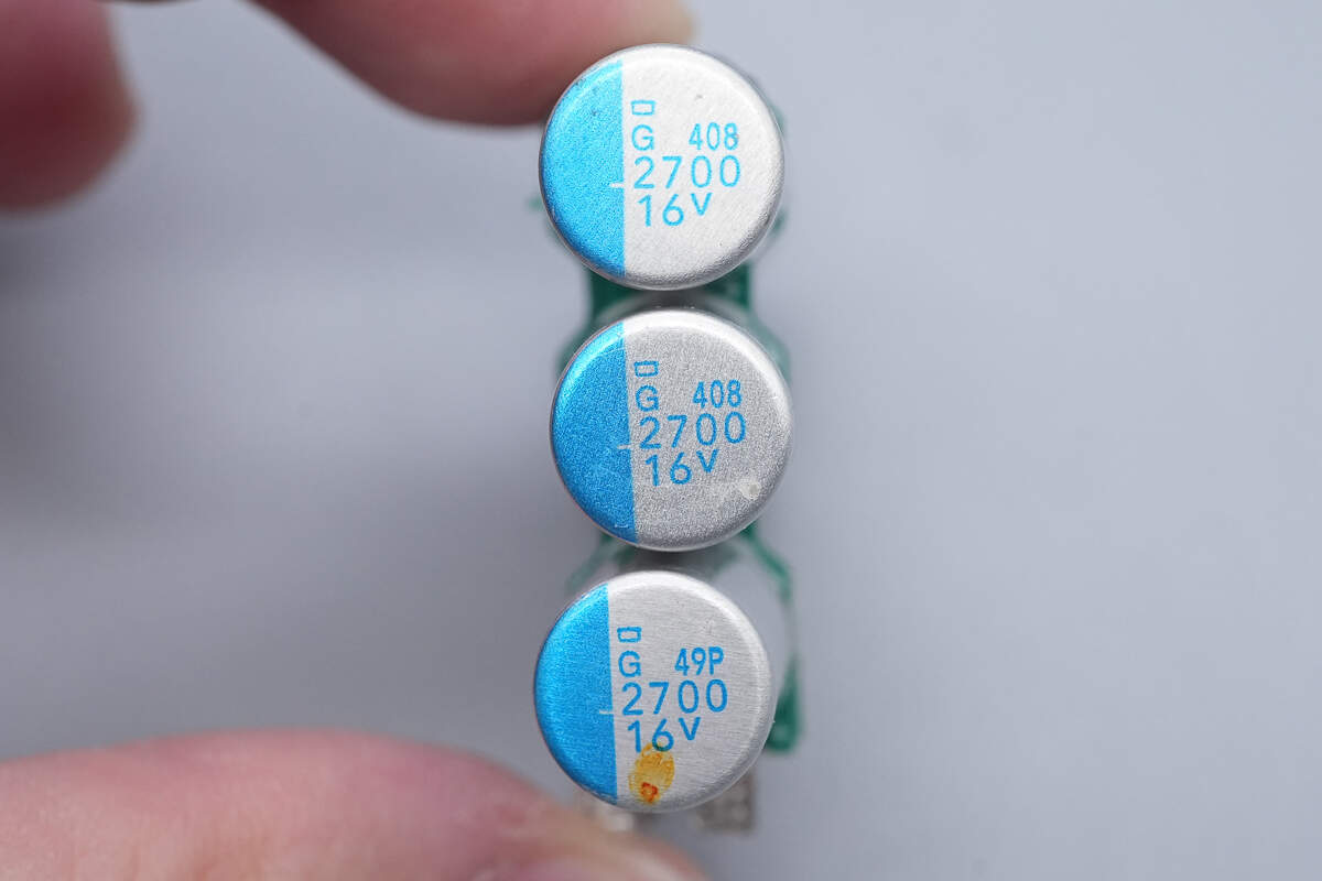
The capacitors are from NCC and are PSG series conductive polymer solid aluminum electrolytic capacitors with a specification of 2700μF 16V.
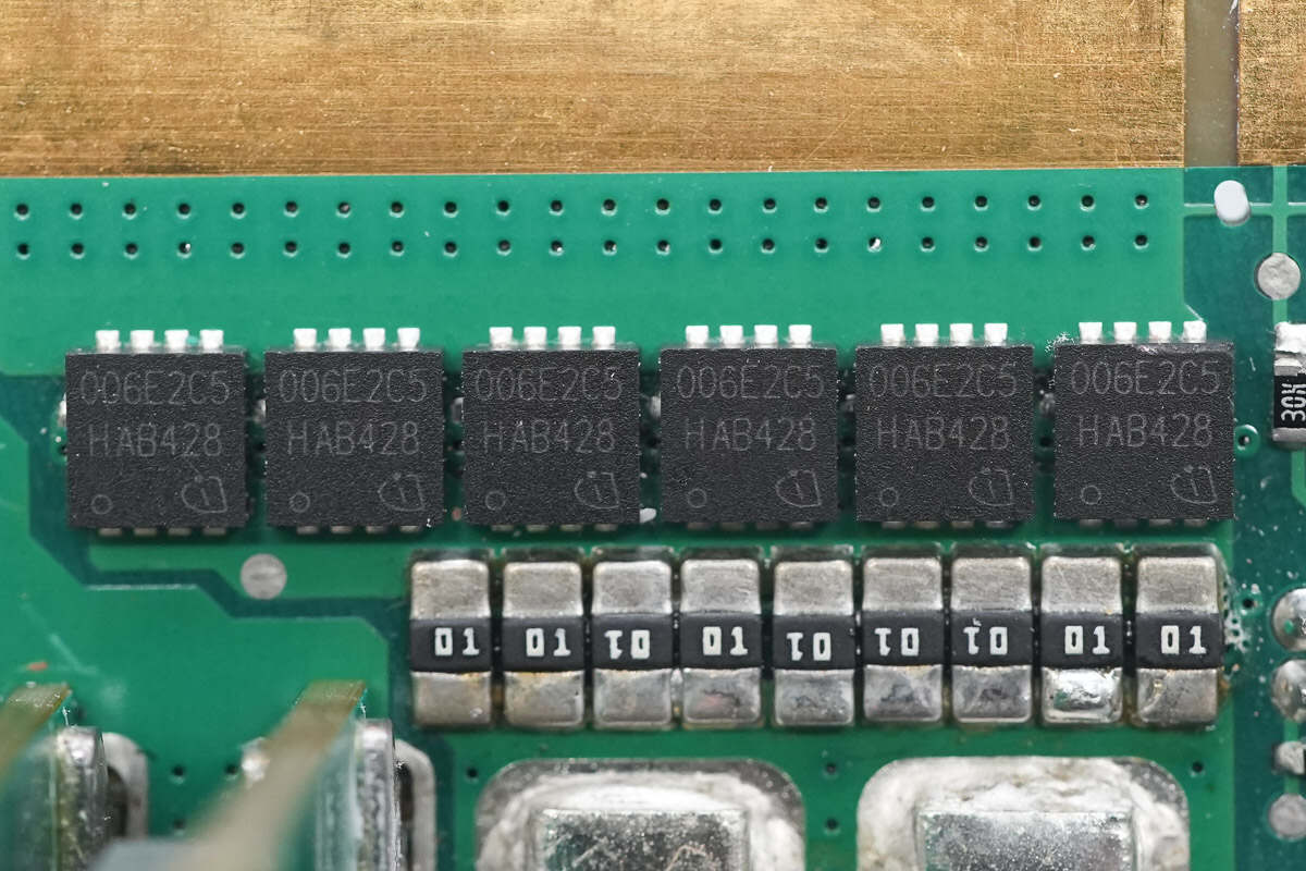
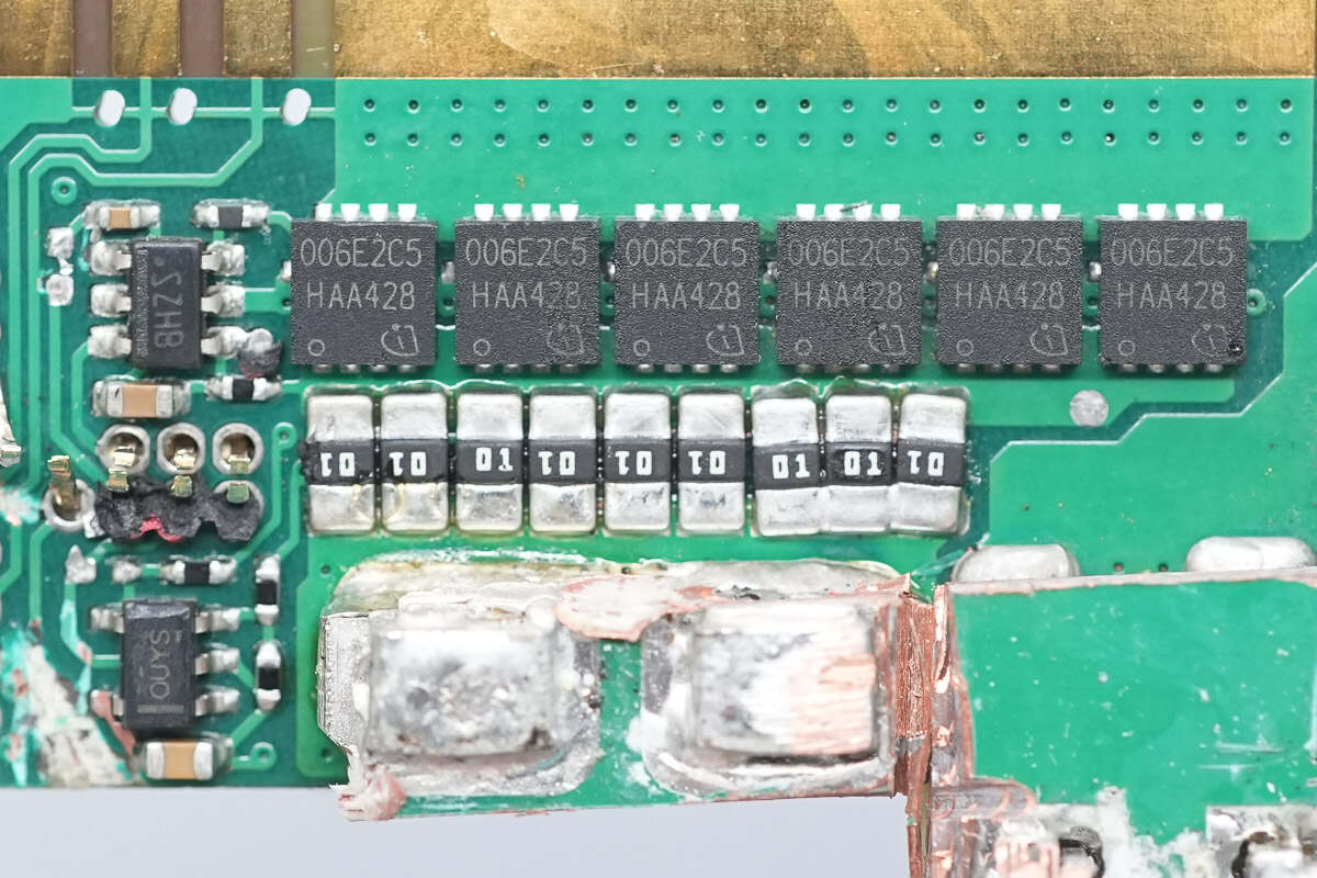
The output control MOSFETs are from Infineon, marked 006E2C5, model IQE006NE2LM5CG. They are NMOS devices with a voltage rating of 25 V and an on-resistance of 0.65 mΩ, packaged in a TTFN-9-1 package.
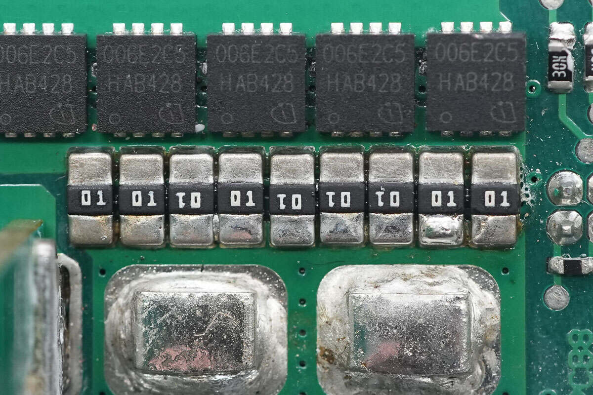
Nine 1 mΩ sense resistors are connected in parallel to measure the output current.
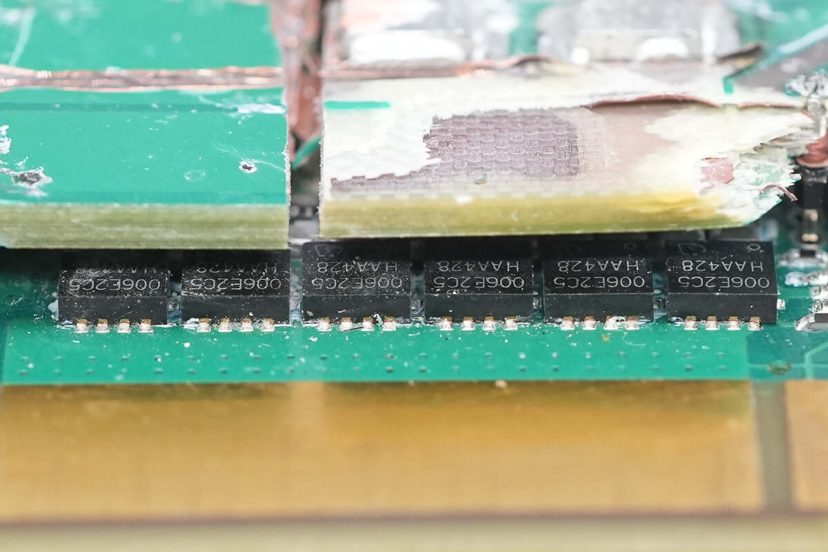
The PCB interlayers also accommodate the output control MOSFETs and the current sense resistors.
The interlayer contains six output control MOSFETs and nine current sense resistors.
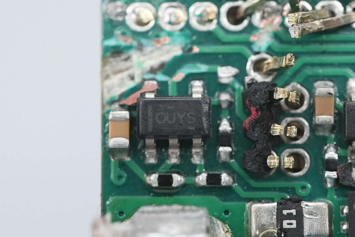
The operational amplifier is from TI, marked OUYS, model OPA192. It is a precision op-amp with low offset voltage, low input bias current, and rail-to-rail input and output, packaged in a SOT-23.
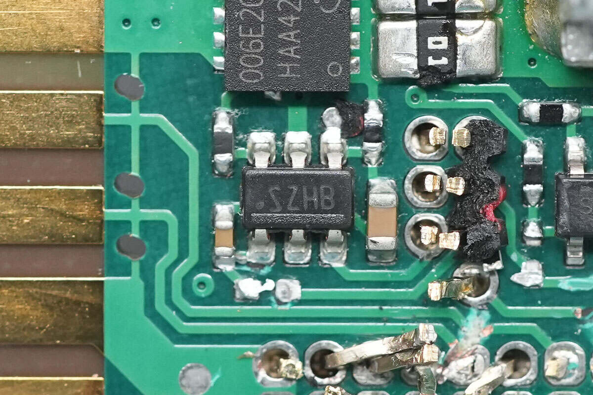
The ideal diode controller is from TI, marked SZHB, model LM5050. It supports an operating voltage of 5–75 V and comes in a SOT-23 package.
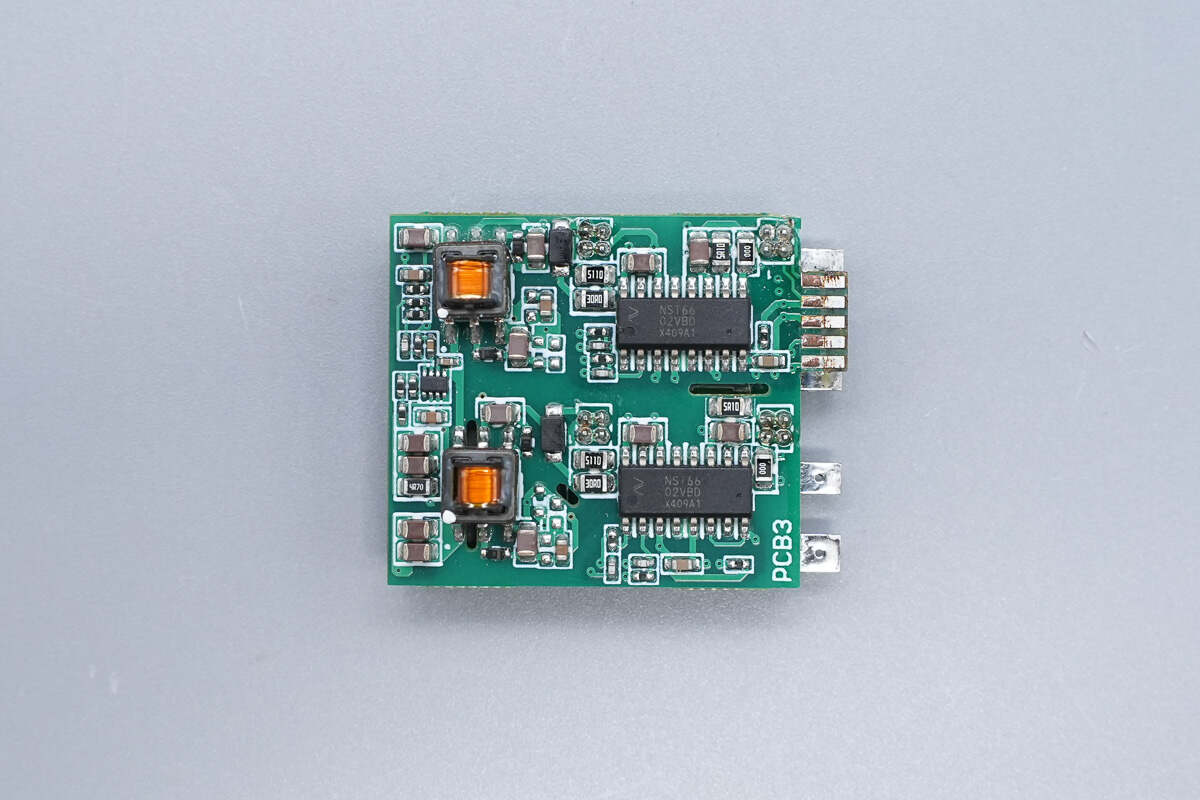
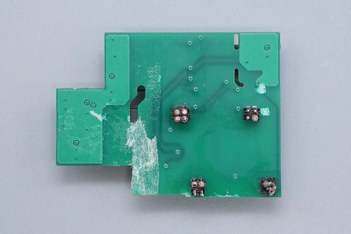
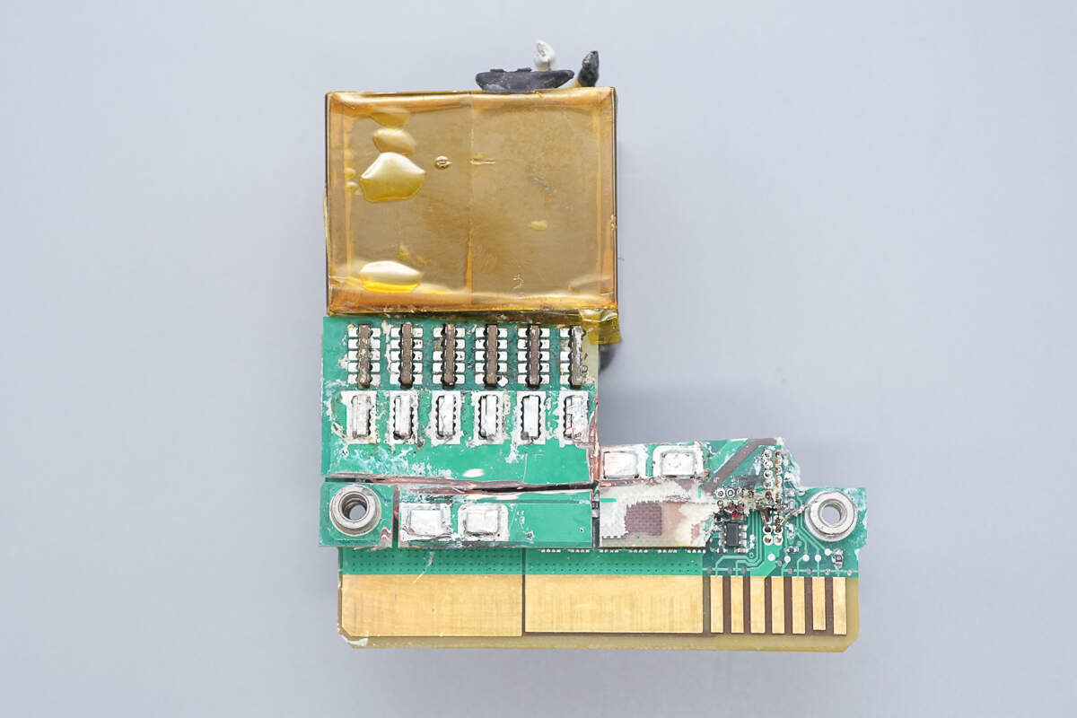
The standby power supply PCB is composed of two PCBs soldered together.
The opposite side contains capacitors.
Upon separating the two PCBs, a mylar sheet was found between them for insulation.
The outer side of the standby power supply PCB houses the standby power chip, synchronous buck chip, feedback optocoupler, and synchronous rectifier.
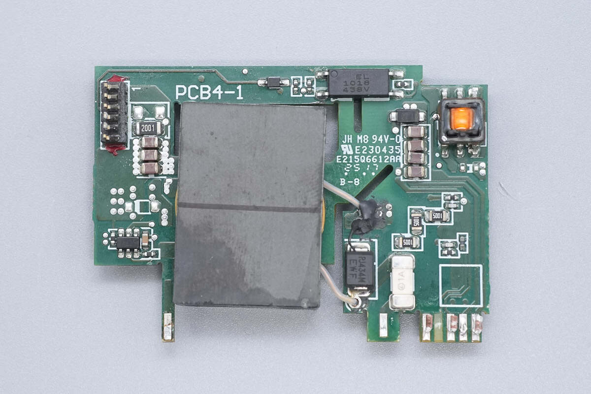
The opposite side features a fuse, an isolation transformer, optocouplers, and a synchronous rectifier controller.
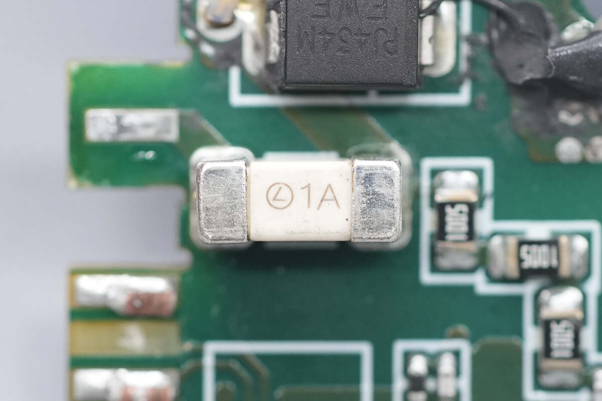
The fuse is rated at 1 A.
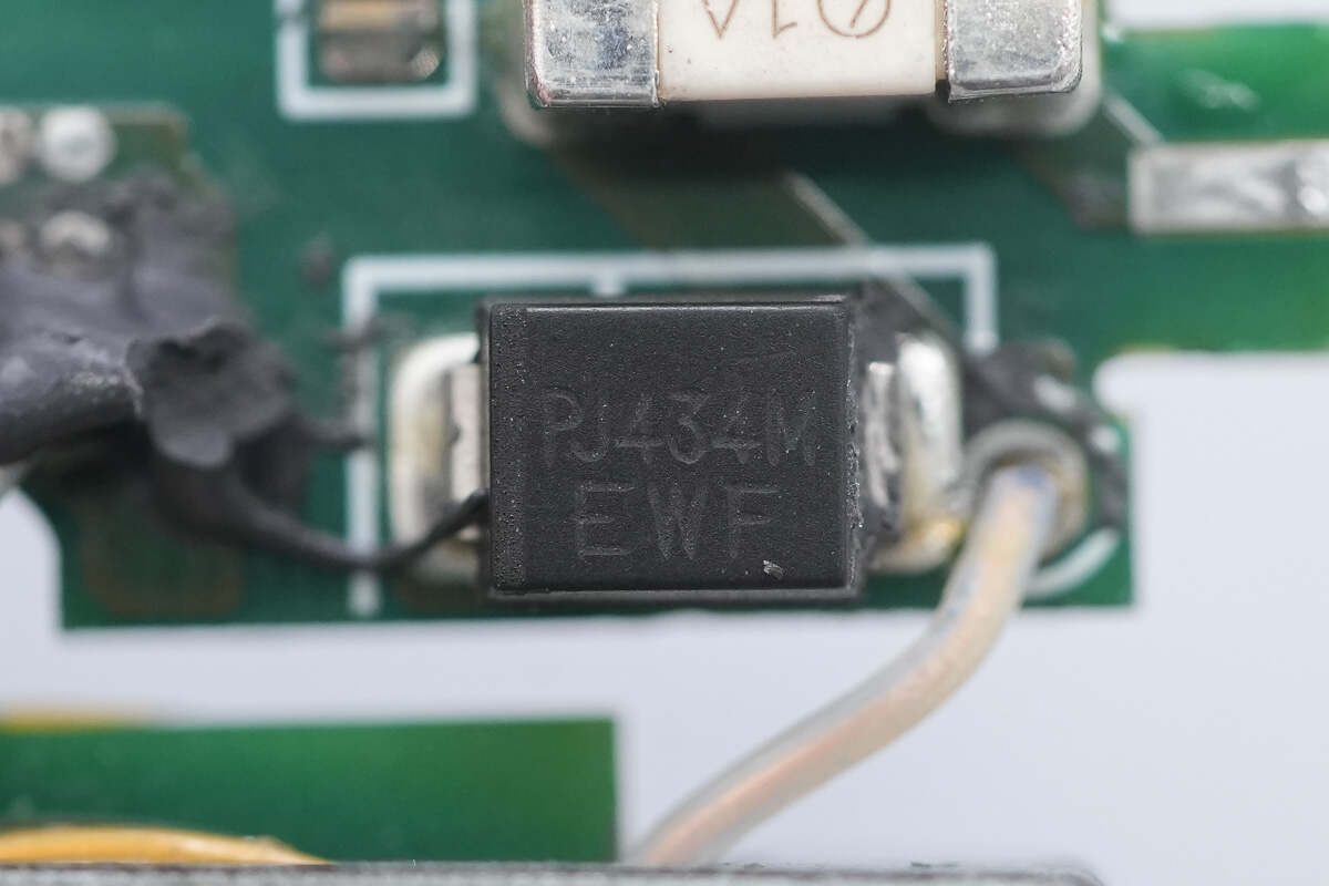
The TVS diode is from PANJIT, marked EWF, model P6SMB250A. It has a working voltage of 214 V and comes in an SMB package.
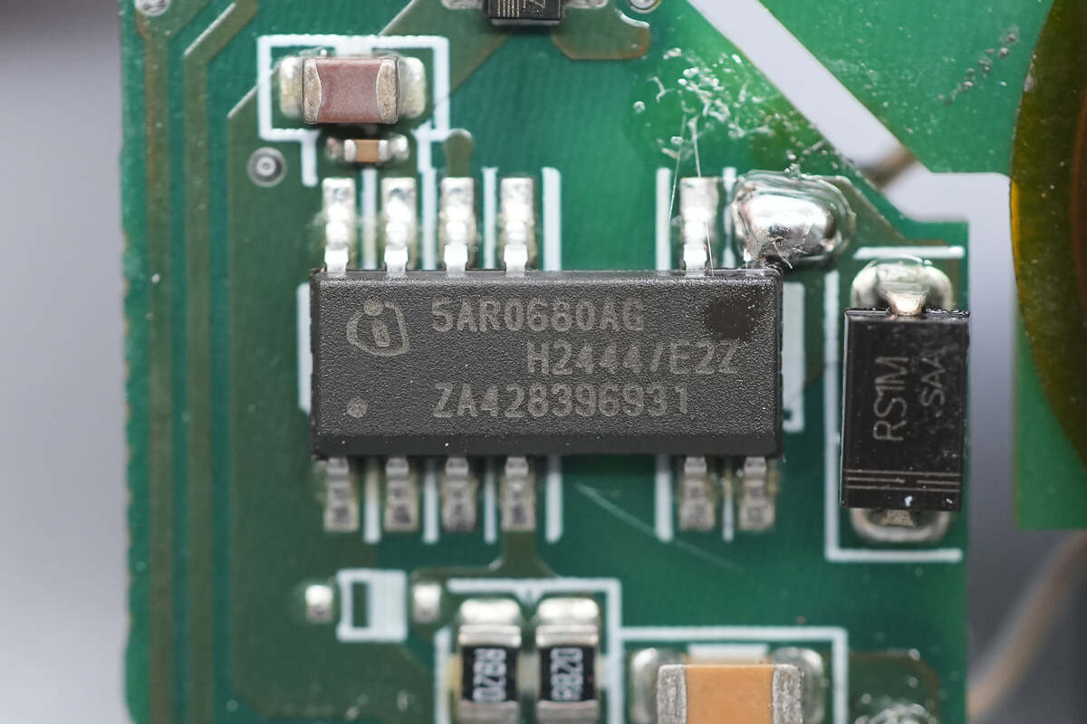
The standby power chip is from Infineon, model ICE5AR0680AG. It integrates an 800 V, 0.71 Ω MOSFET, operates at a switching frequency of 100 kHz, supports a wide input voltage range with 40 W output power, and comes in a DSO-12 package.
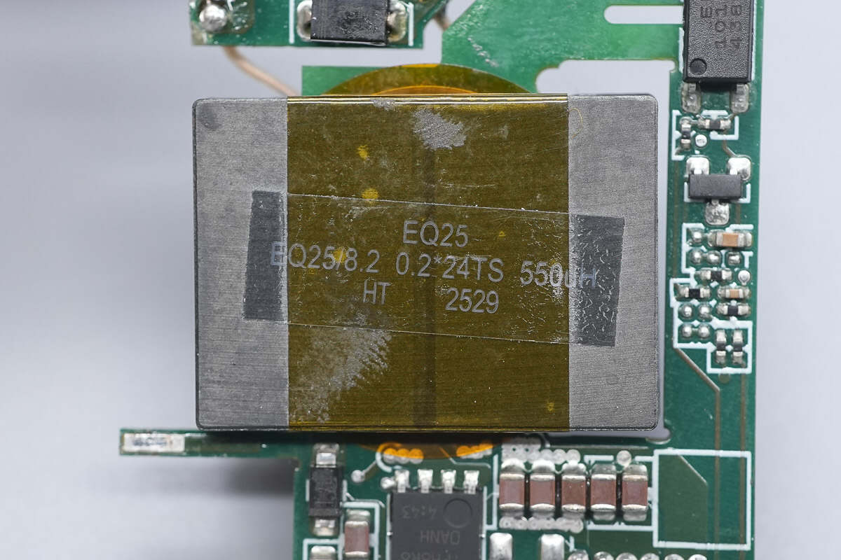
The planar transformer uses an EQ25 magnetic core.
The synchronous buck chip is a TI TPS62933F.
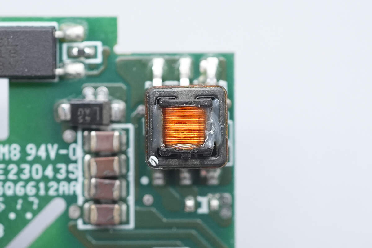
Close-up of the isolation transformer.
Close-up of the MLCC filter capacitors.
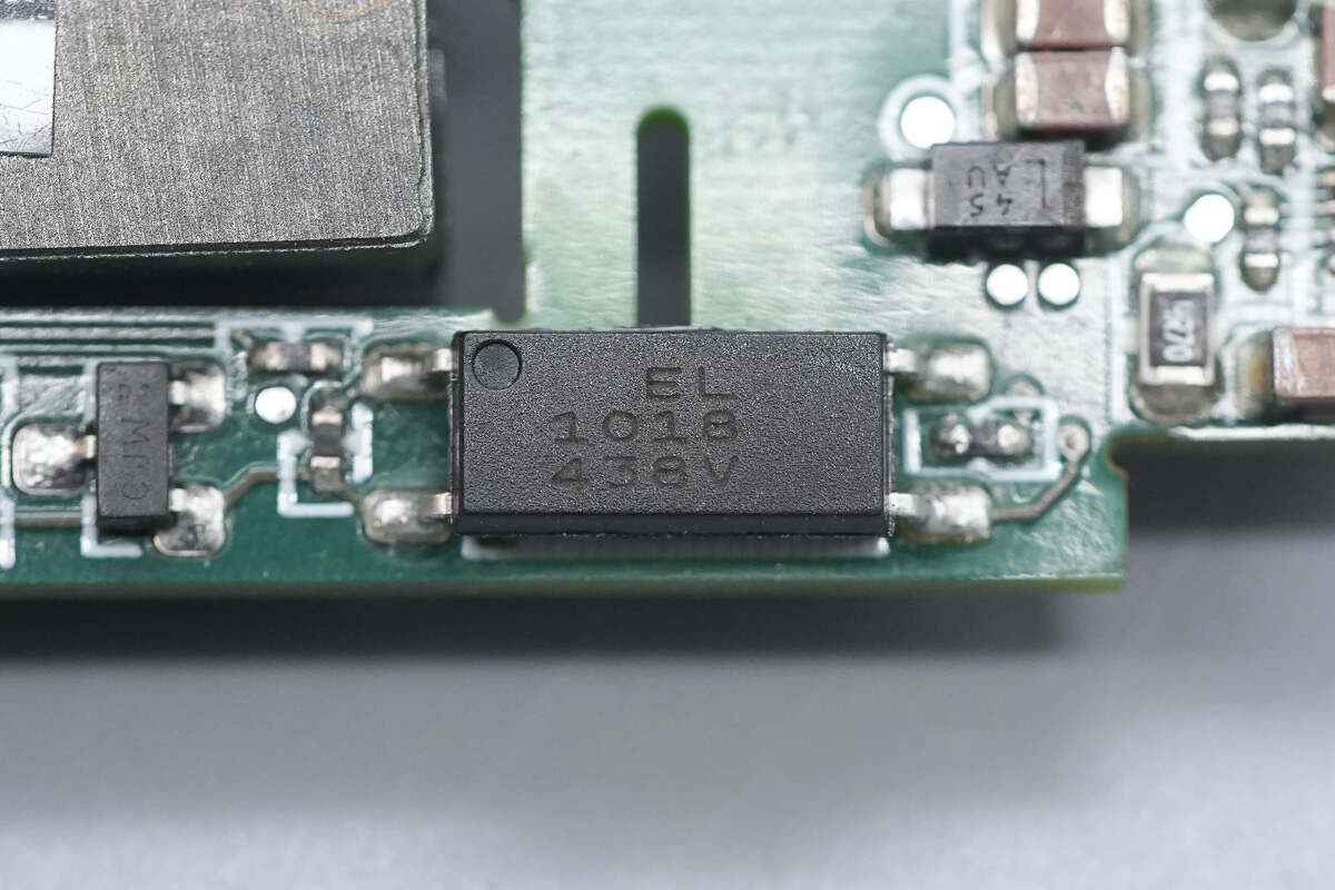
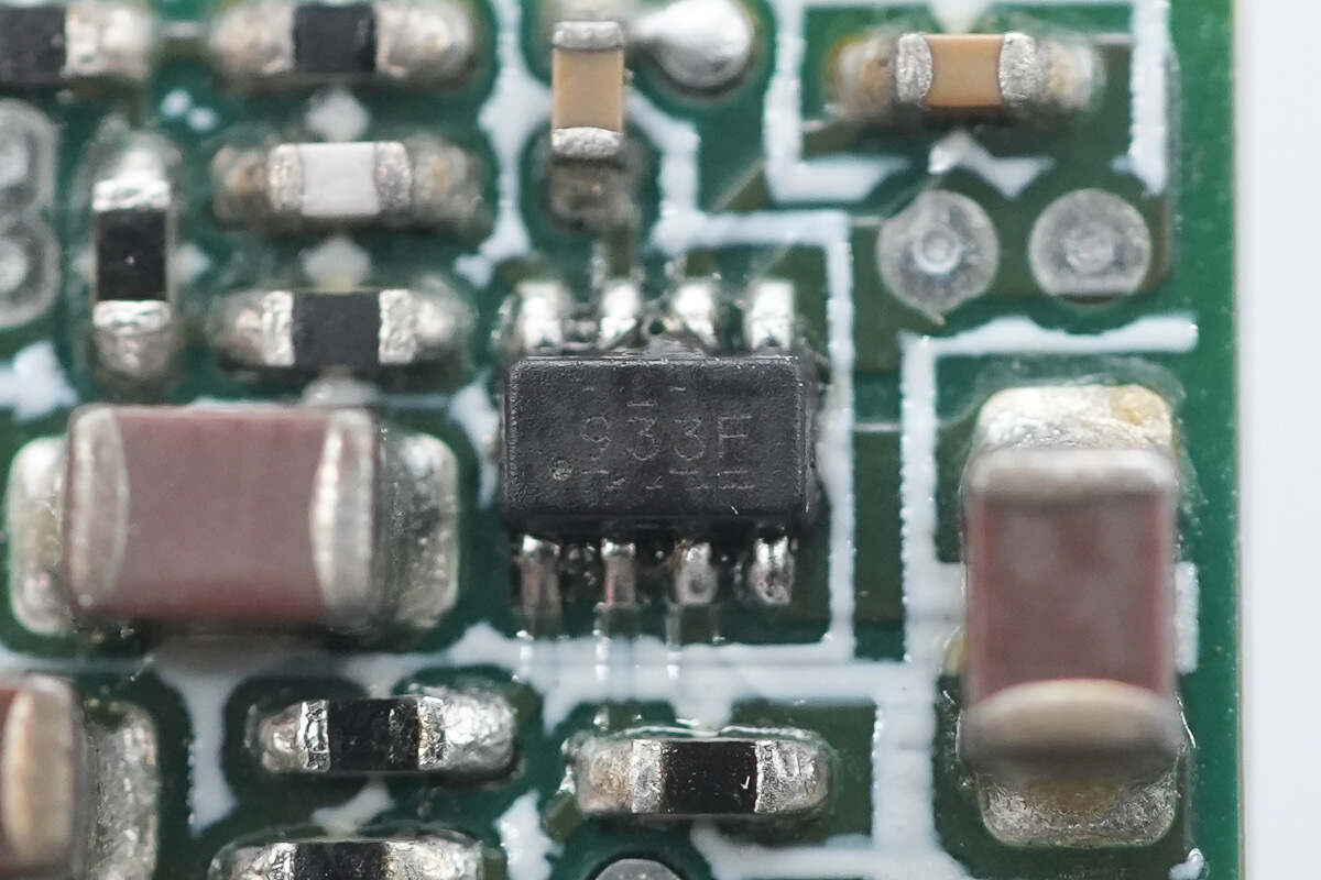
Close-up of the Everlight EL1018 optocoupler.
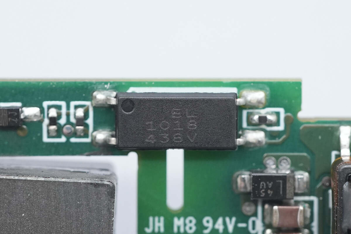
The other optocoupler has the same model.
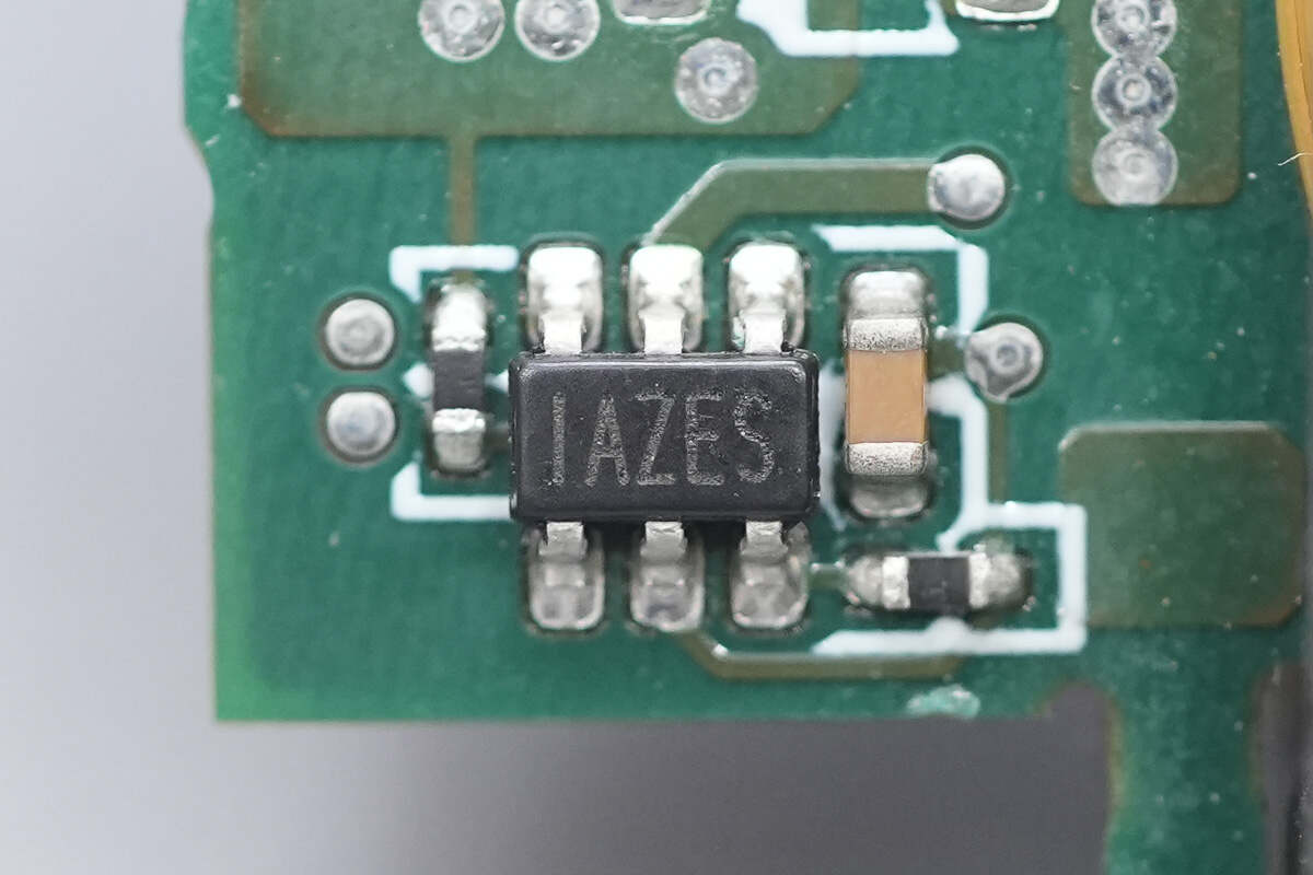
The synchronous rectifier controller is from MPS, marked IAZE, model MP6908. It supports high-side and low-side synchronous rectification without an auxiliary winding, features built-in ringing detection, and is compatible with synchronous rectifiers using standard or logic-level voltages. It supports DCM, CCM, and QR operating modes and comes in a TSOT-23-6 package.
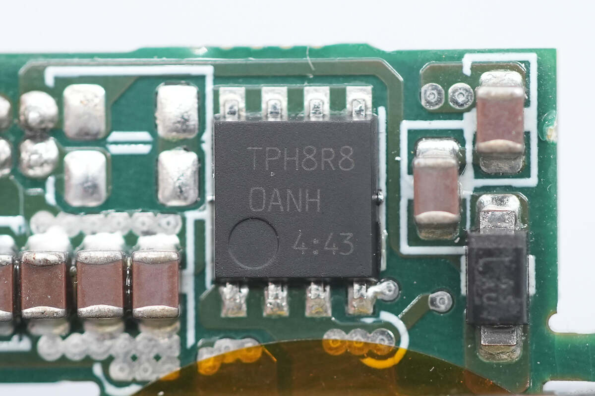
The synchronous rectifier is from Toshiba, model TPH8R80ANH. It is an NMOS device with a voltage rating of 100 V and an on-resistance of 7.4 mΩ, packaged in an SOP Advance package.
Close-up of MLCC filter capacitors.
The other PCB features filter capacitors and a load switch.
The back side has no components.
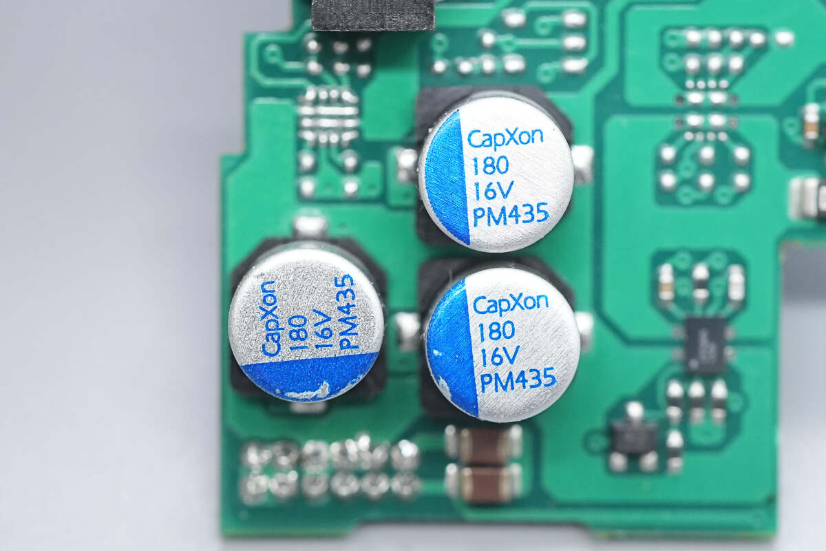
The filter capacitors are from CapXon, part of the PM series of solid capacitors, with a rating of 180 μF, 16 V.
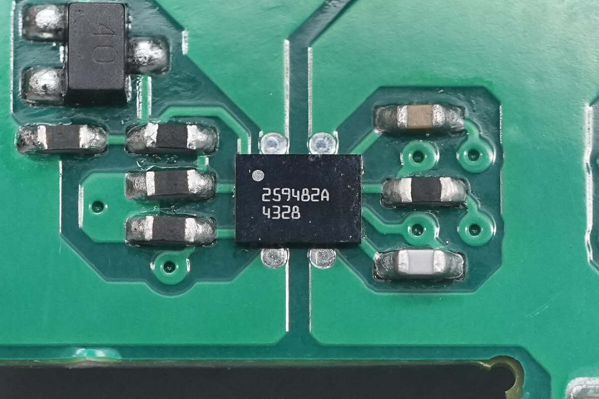
The load switch is from TI, model TPS259482A. It supports an operating voltage range of 3.5–23 V, features a built-in 12.2 mΩ protection FET, supports an 8 A operating current, and comes in a PWCSP12 package.
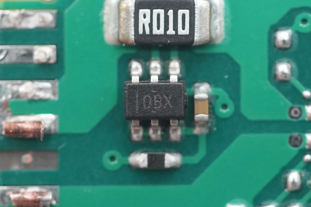
The current-sense amplifier is from TI, marked OBX, model INA213. It is a 26 V bidirectional high-precision current-sense amplifier compliant with the AEC-Q100 standard, packaged in SC-70.
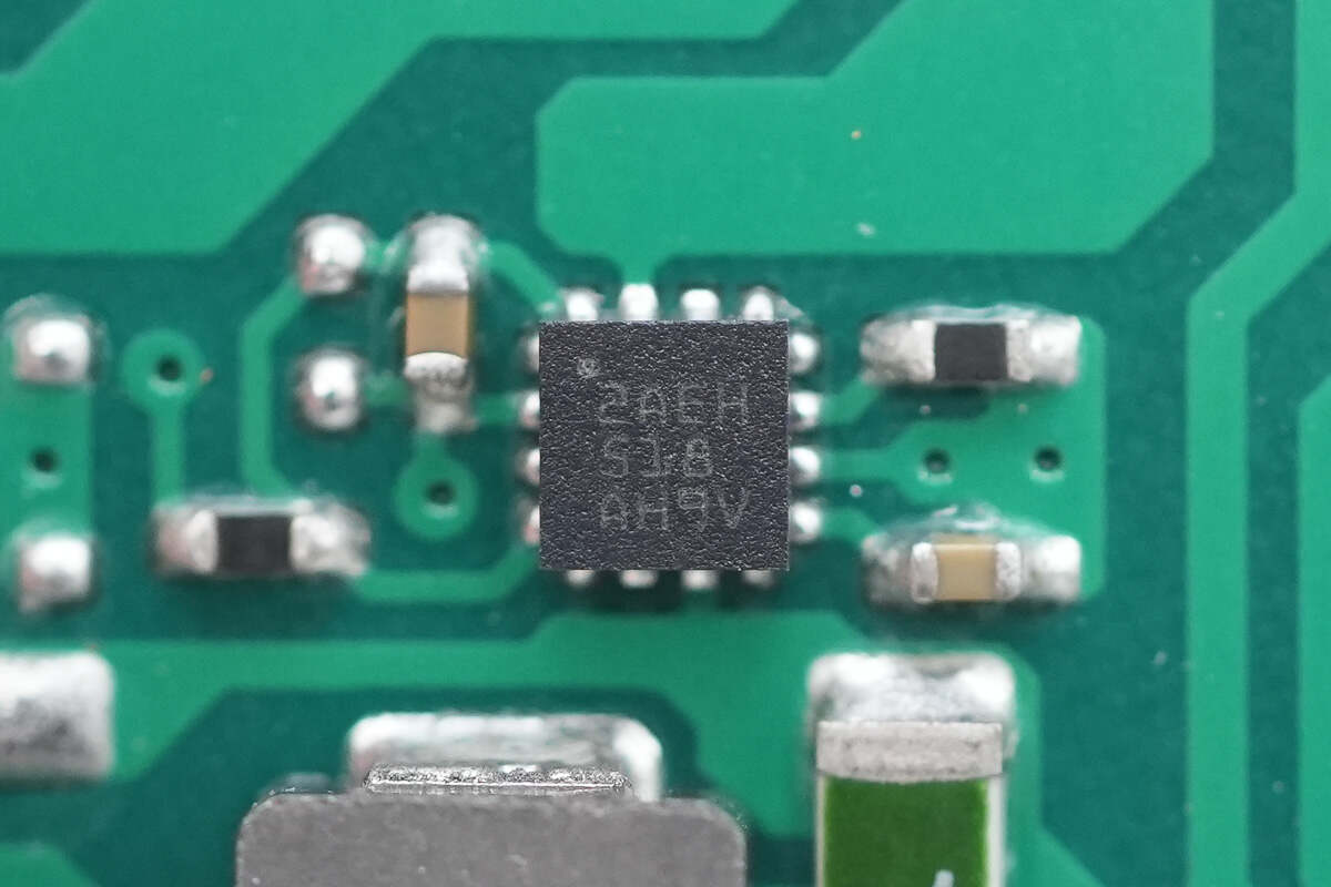
The ideal diode is from TI, marked 2AEH, model LM73100. It features reverse-polarity and overvoltage protection, supports an operating voltage range of 2.7–23 V, includes a 28.4 mΩ internal FET, supports a 5.5 A operating current, and comes in a QFN-10 package.
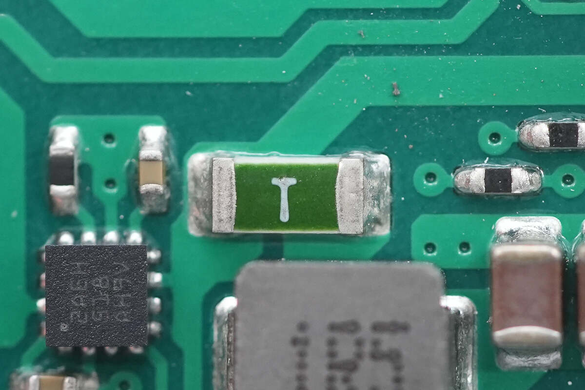
Close-up of an SMD fuse marked with T.

Close-up of the 1.5μH alloy inductor.
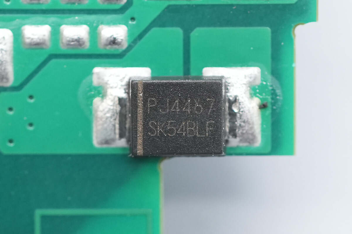
The Schottky diode is from PANJIT, model SK54BLF, rated 40 V, 5 A, and comes in an SMBF package.
Close-up of the socket for connecting the cooling fan.
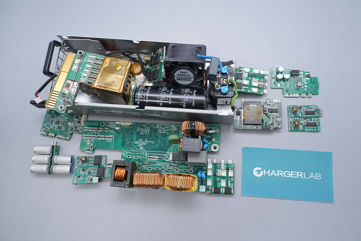
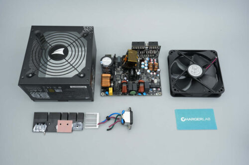
Well, those are all components of the Segotep 3200W Titanium-Rated SiC Digital Server Power Supply.
Summary of ChargerLAB
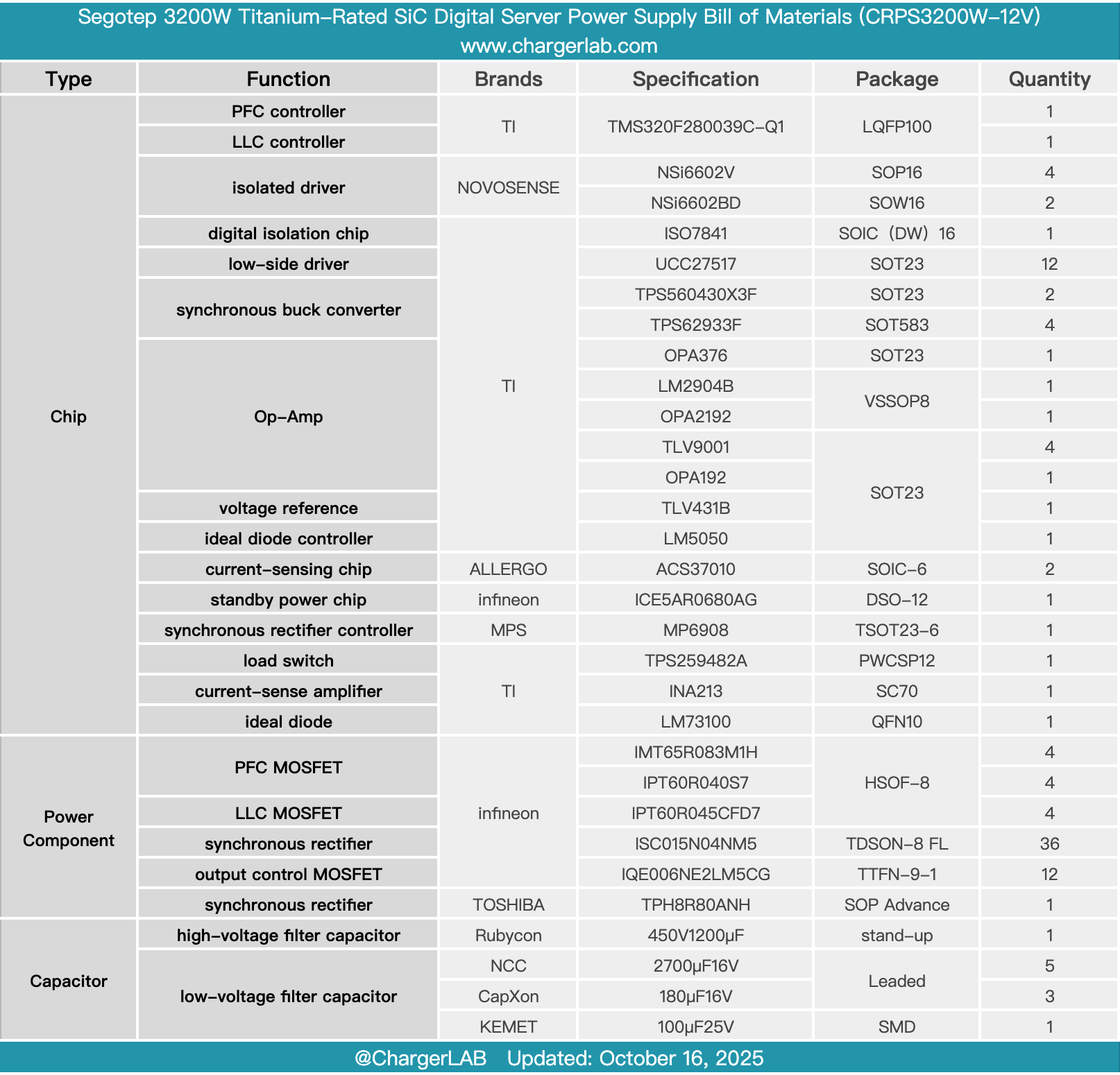
Here is the component list of the Segotep 3200W Titanium-Rated SiC Digital Server Power Supply for your convenience.
It supports a wide input voltage range, with a rated output power of 3200 W. The main output is rated at 12.2 V and 262.3 A, while the standby output is 12 V at 3 A. The built-in cooling fan draws air from the DC output side and exhausts it toward the AC input side for heat dissipation.
After taking it apart, we found that it uses a TI fully digital control solution, with two TMS320F280039C-Q1 DSPs for Totem-Pole PFC and full-bridge LLC control. The interleaved Totem-Pole PFC employs Infineon IMT65R083M1H SiC MOSFETs paired with IPT60R040S7 MOSFETs, driven via NOVOSENSE NSi6602V isolated drivers.
The full-bridge LLC uses Infineon IPT60R045CFD7 MOSFETs with NOVOSENSE NSi6602BD isolated drivers. Synchronous rectifiers employ ISC015N04NM5 MOSFETs, driven by Texas Instruments UCC27517 drivers. The standby power supply uses the Infineon ICE5AR0680AG switching power chip paired with the MPS MP6908 synchronous rectifier controller. High-voltage filter capacitors are from Rubycon, while output filter capacitors are from NCC. The internal PCBs are soldered together to maximize space utilization, and the construction and component selection are solid and reliable.
Related Articles:
1. Teardown of Xiaomi 33W Nano Power Adapter (MDY-19-ED)
2. Teardown of UGREEN 22.5W 20000mAh Power Bank with Built-in Cable (PB505)
3. Teardown of EcoFlow RAPID Pro 320W GaN Desktop Charger (EF-DC-320)