Introduction
We obtained a Pisen GaN charger featuring four USB-C ports and a maximum total output of 160W. In terms of performance, the USB-C3 and USB-C4 ports each support up to 140W with PD 3.1, while the USB-C1 and USB-C2 ports support up to 20W. The charger also supports multiple power distribution modes, including 140W + 20W, 100W + 60W, and 65W + 65W + 20W, enabling fast charging for multiple devices such as laptops, tablets, and smartphones simultaneously. Next, we will take a closer look at the detailed design of this PISEN product.
Product Appearance
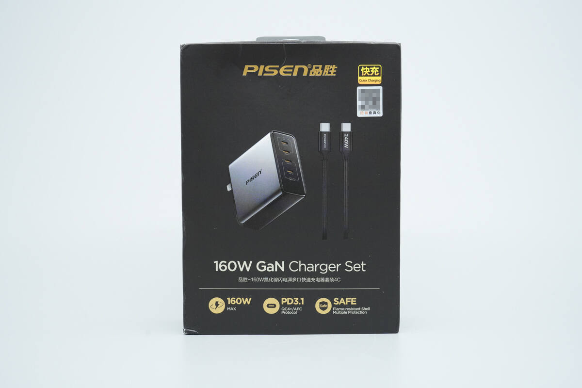
The front of the packaging features the PISEN logo, the product name, an image of the charger, and key selling points.
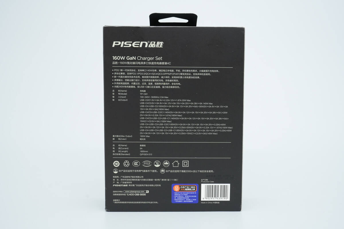
The back of the packaging displays specifications and other related information.

The package includes the charger, a cable, and a warranty card.
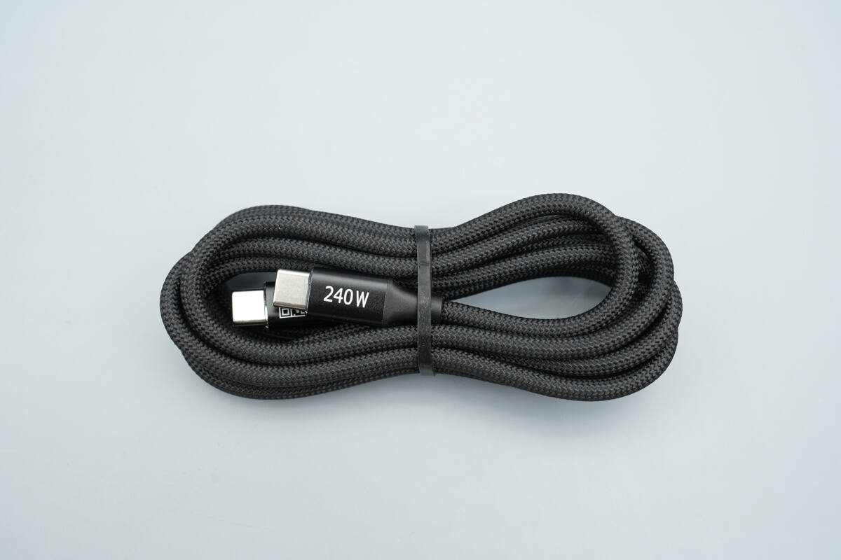
The included dual USB-C cable features a braided design.
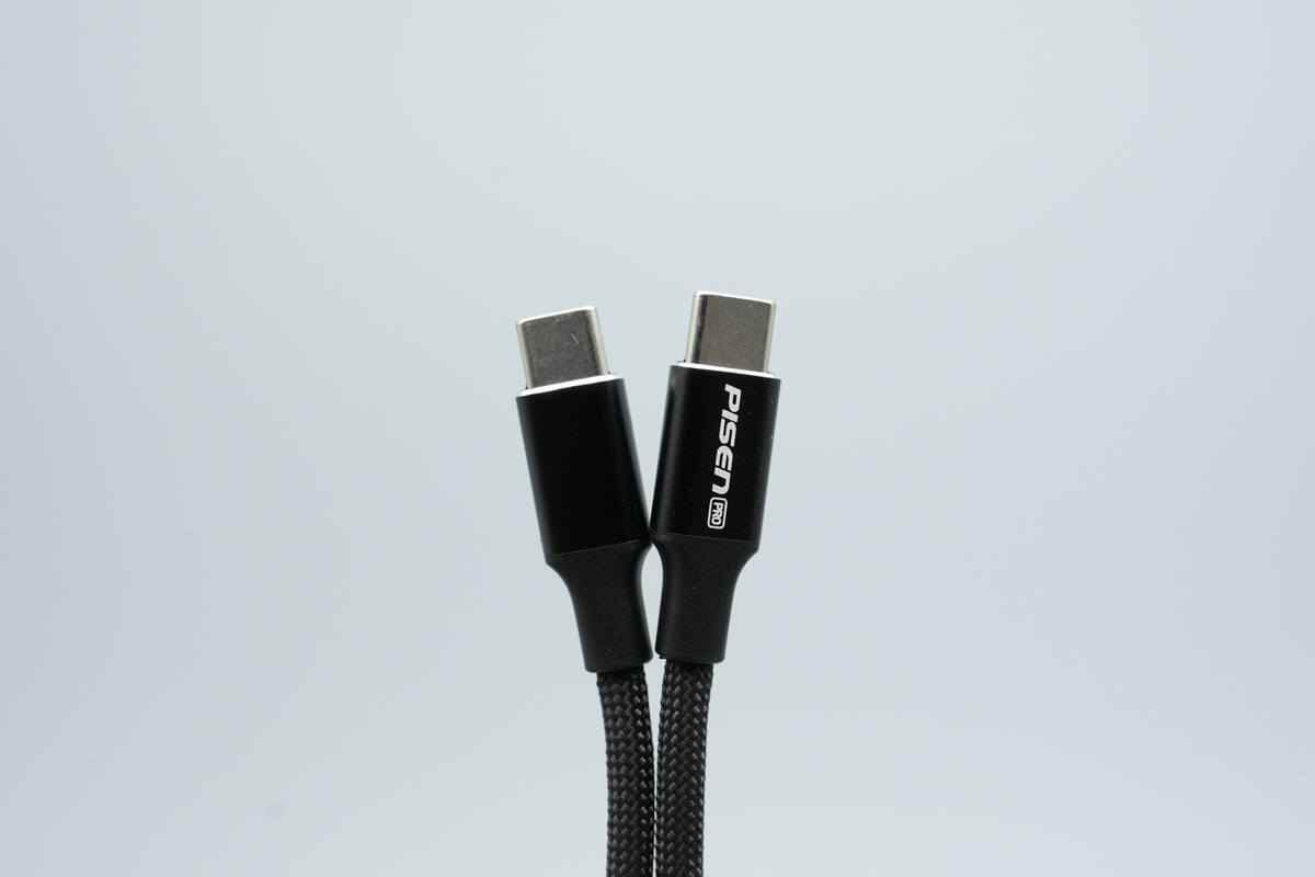
The connector housings are made of metal.
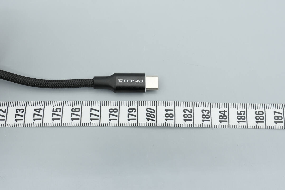
The length of the cable is about 1.8 m (approximately 71 inches).
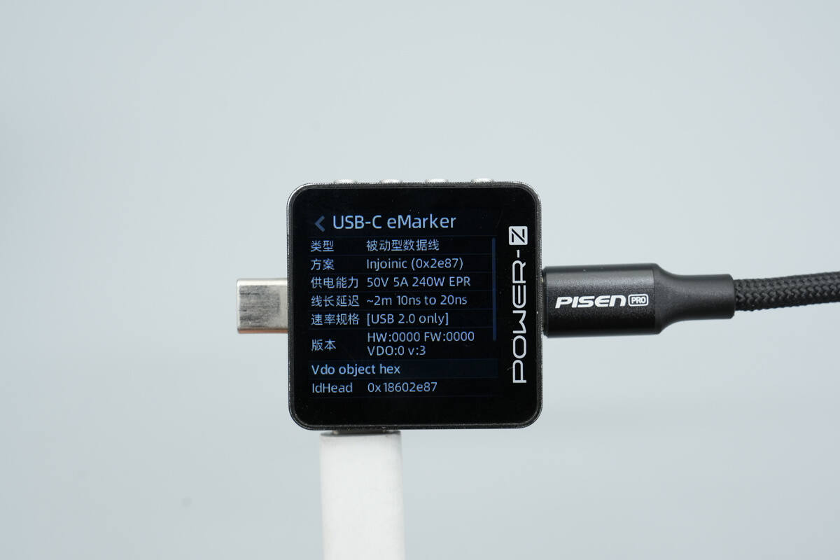
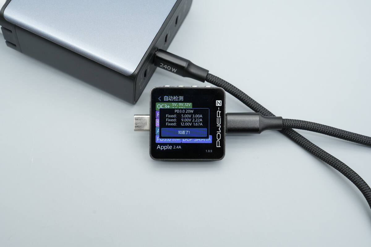
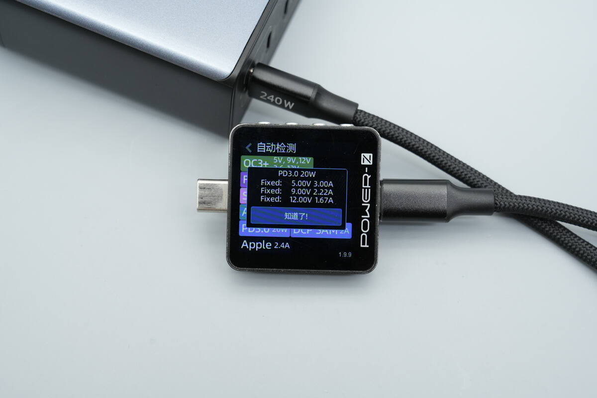
ChargerLAB POWER-Z KM003C shows that the cable is equipped with an Injoinic E-Marker chip, supporting a power delivery capability of 50V 5A and data transmission at USB 2.0 speeds.

The outer casing is made of flame-retardant PC material.
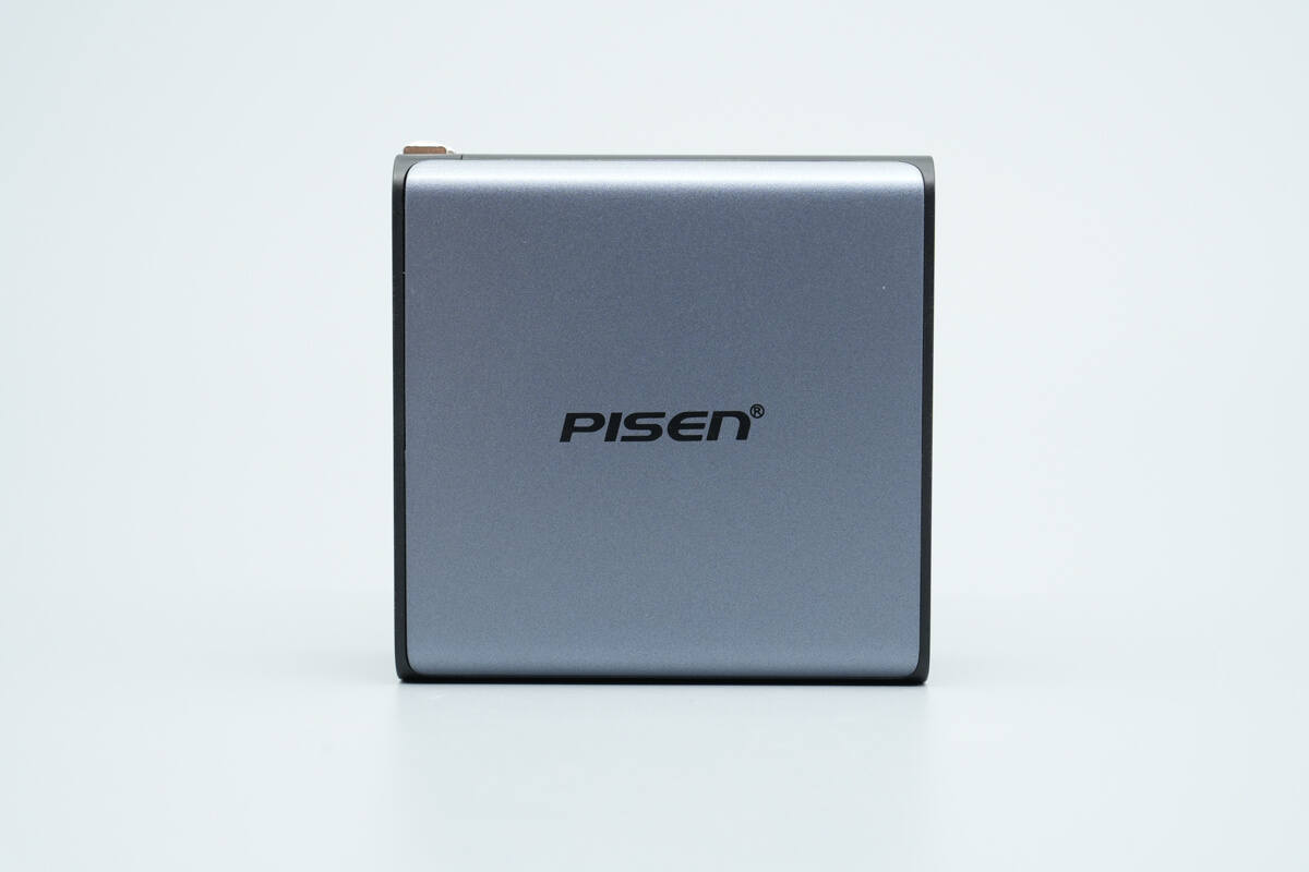
The front center of the charger is marked with the PISEN logo.
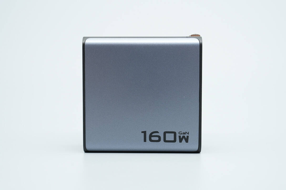
The back is marked with "160W GaN."

The input port housing is marked with the specifications.
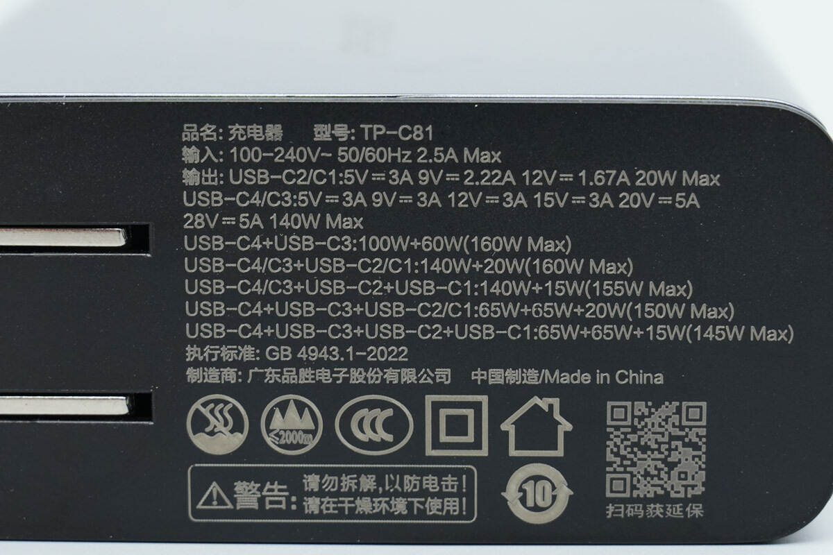
Model: TP-C81
Input: 100–240V~ 50/60Hz 2.5A Max
Output:
USB-C2/C1: 5V 3A, 9V 2.22A, 12V 1.67A, 20W Max
USB-C4/C3: 5V 3A, 9V 3A, 12V 3A, 15V 3A, 20V 5A, 28V 5A, 140W Max
USB-C4 + USB-C3: 100W + 60W (160W Max)
USB-C4/C3 + USB-C2/C1: 140W + 20W (160W Max)
USB-C4/C3 + USB-C2 + USB-C1: 140W + 15W (155W Max)
USB-C4 + USB-C3 + USB-C2/C1: 65W + 65W + 20W (150W Max)
USB-C4 + USB-C3 + USB-C2 + USB-C1: 65W + 65W + 15W (145W Max)
The charger is CCC certified.
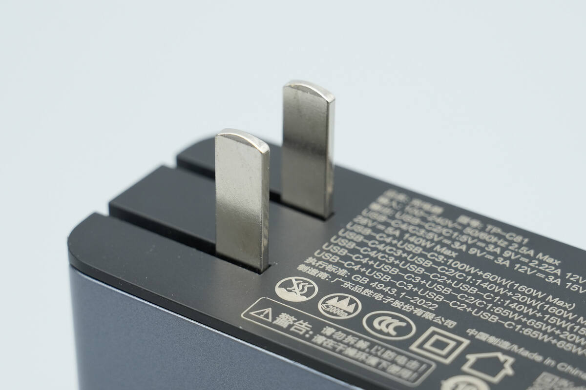
It is equipped with foldable plug pins.
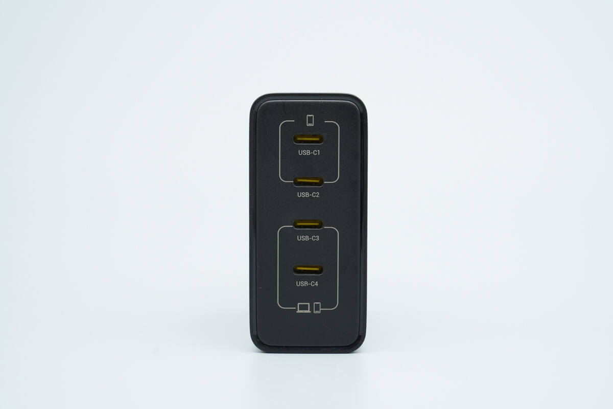
The output side features four USB-C ports, each marked with its corresponding label.
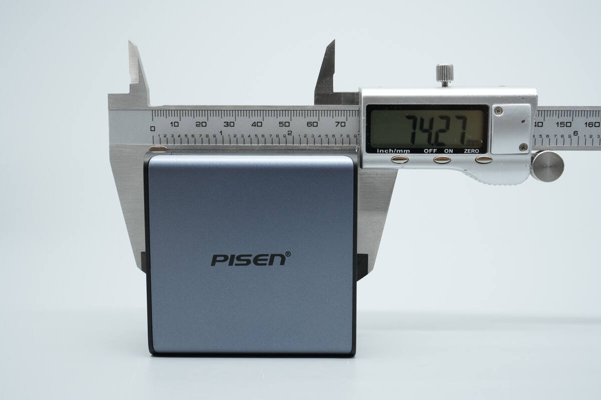
The length of the charger is about 74.27 mm (2.92 inches).
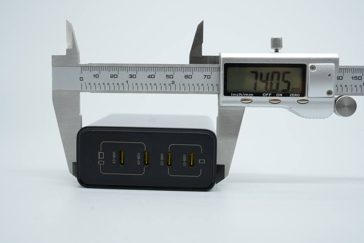
The width is about 74.05 mm (2.92 inches).
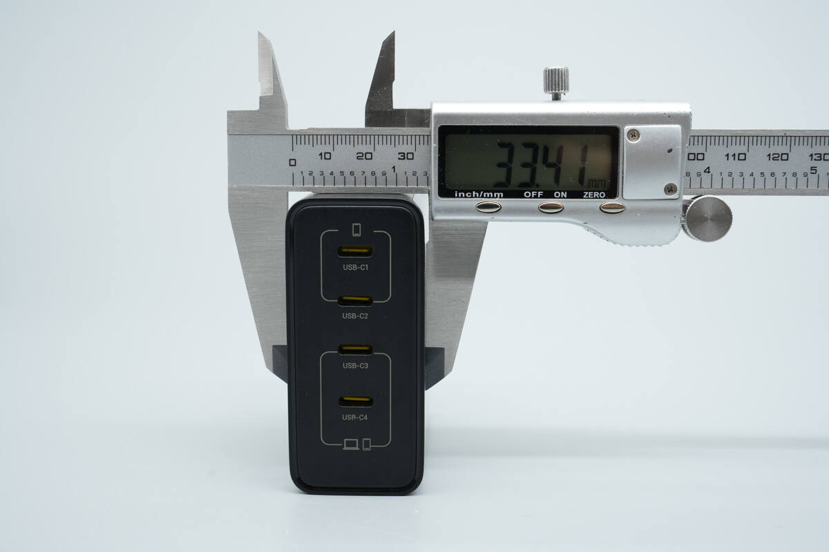
The thickness is about 33.41 mm (1.32 inches).
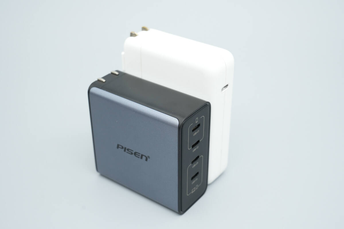
It is slightly smaller in size compared to the Apple 140W charger.
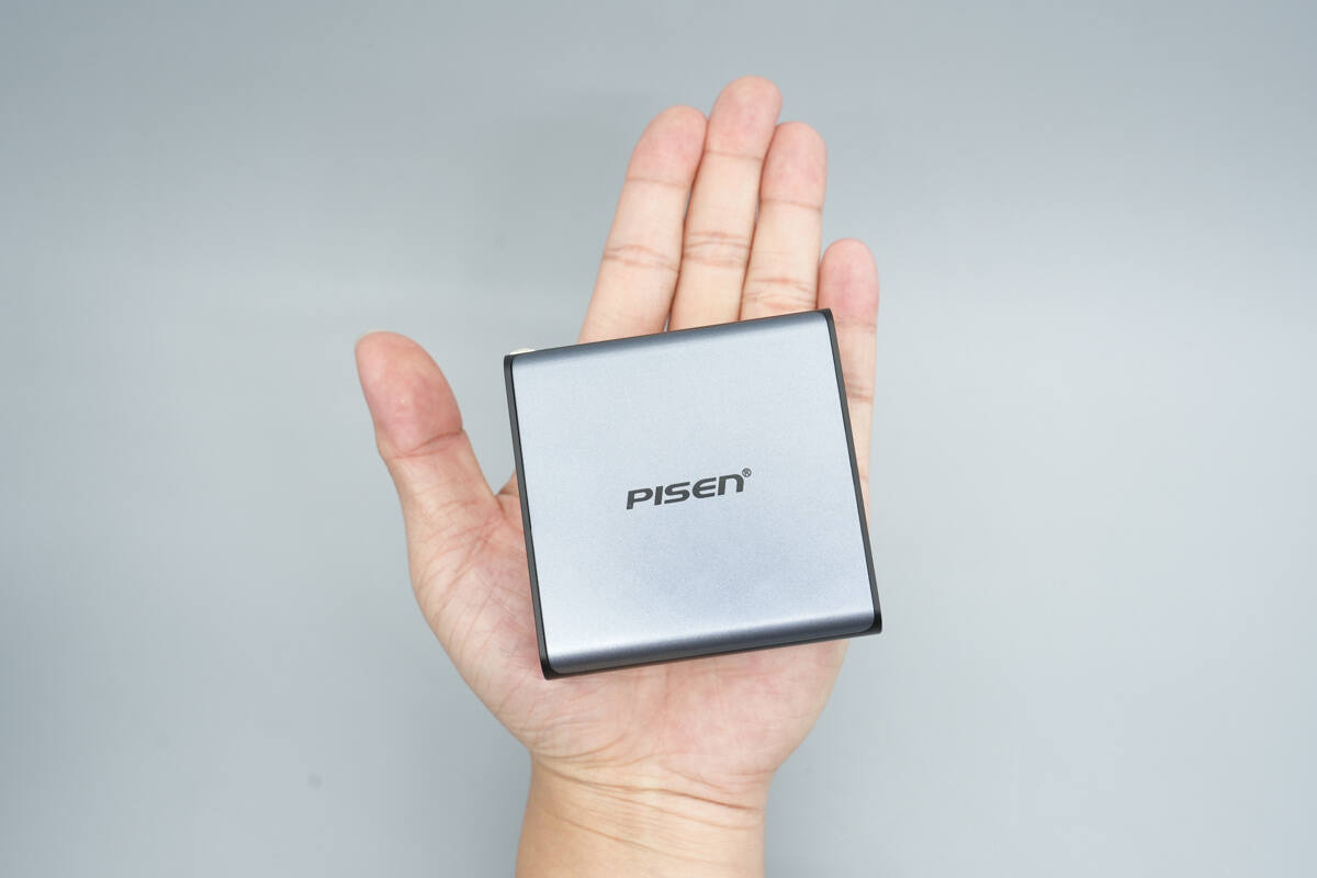
That's how big it is on the hand.
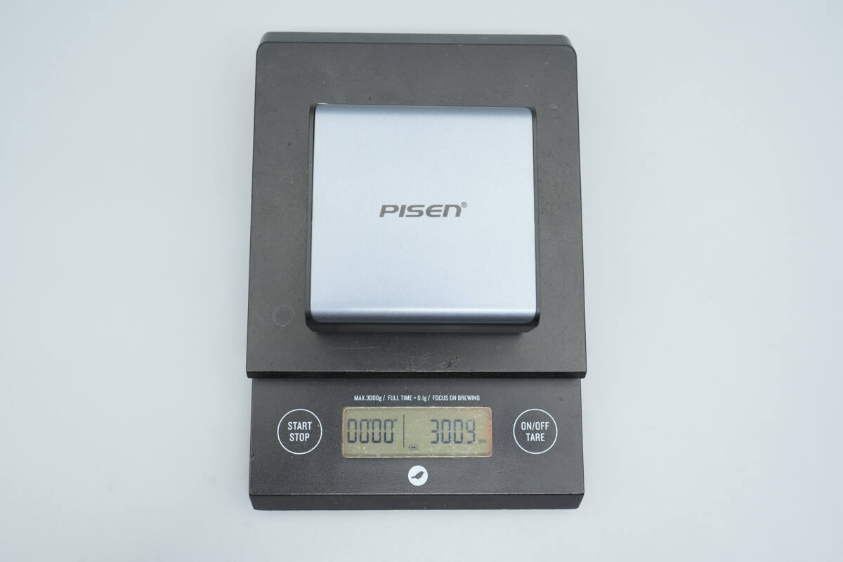
The weight is about 301 g (10.62 oz).
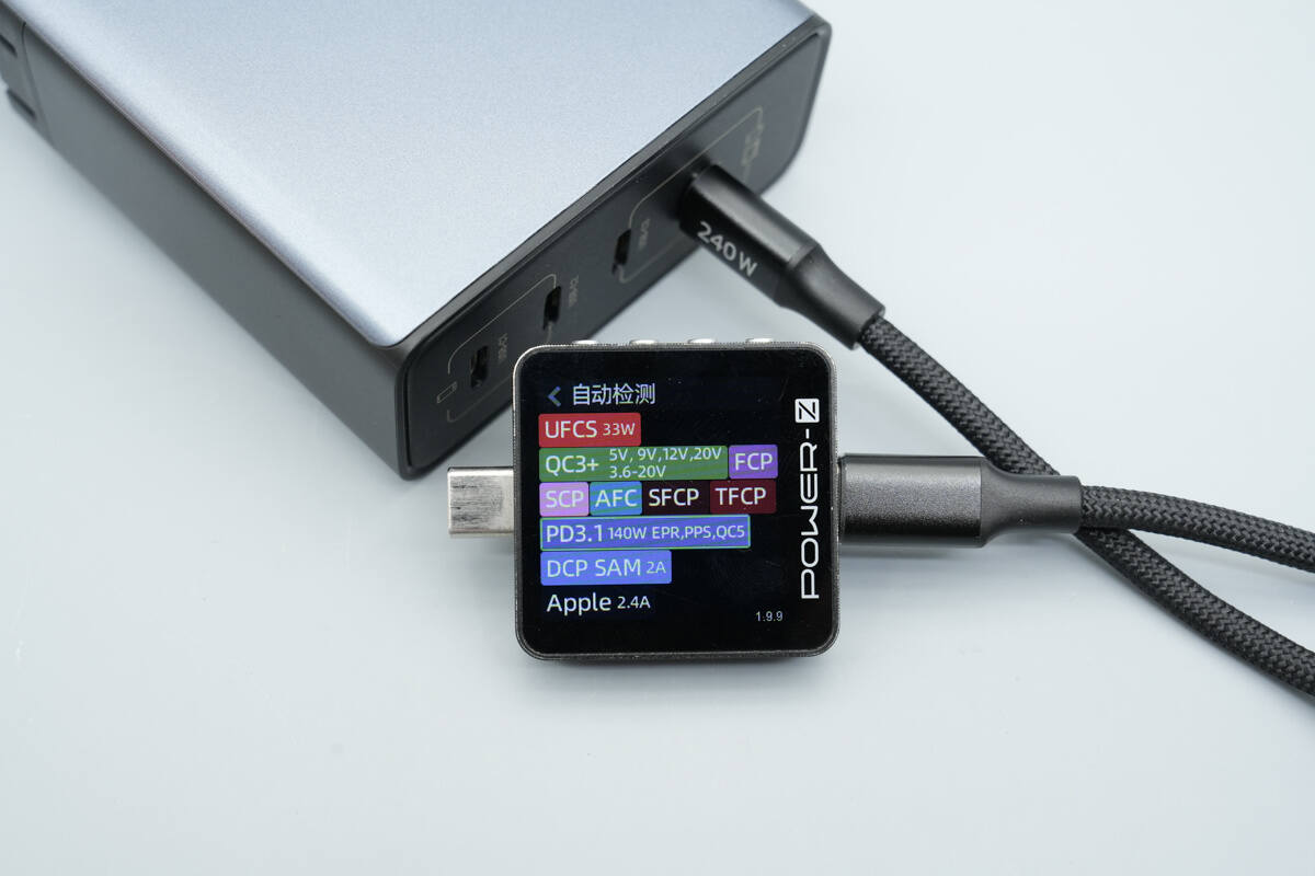
ChargerLAB POWER-Z KM003C shows that the USB-C4 supports UFCS, QC3+/5, FCP, SCP, AFC, SFCP, TFCP, PD3.1, PPS, DCP, SAM 2A, and Apple 2.4A protocols.
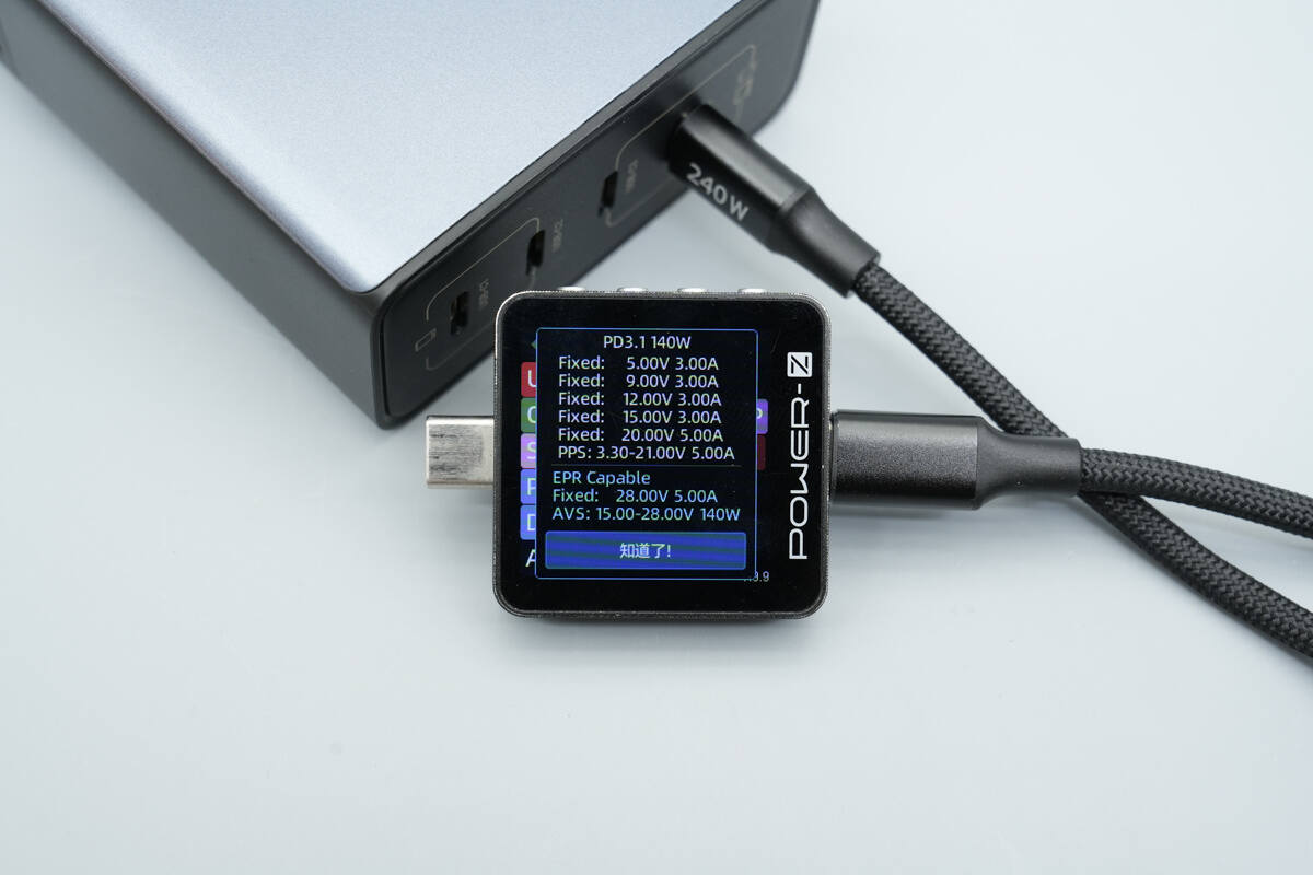
It has six fixed PDOs of 5V 3A, 9V 3A, 12V 3A, 15V 3A, 20V 5A, and 28V 5A, as well as a PPS voltage range of 3.3–21V 5A and an AVS voltage range of 15–28V 140W.
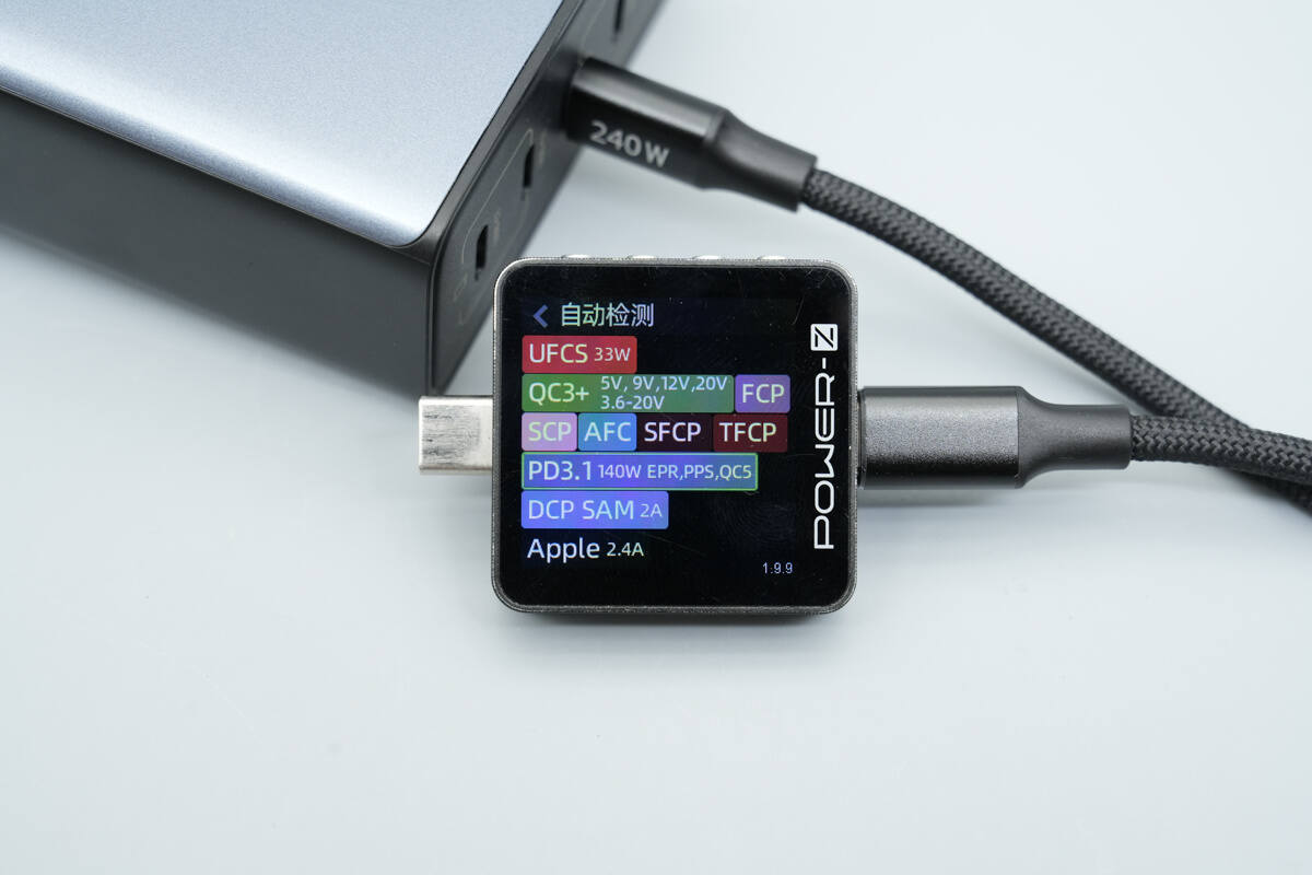
The USB-C3 port supports the same protocols as the USB-C4 port.
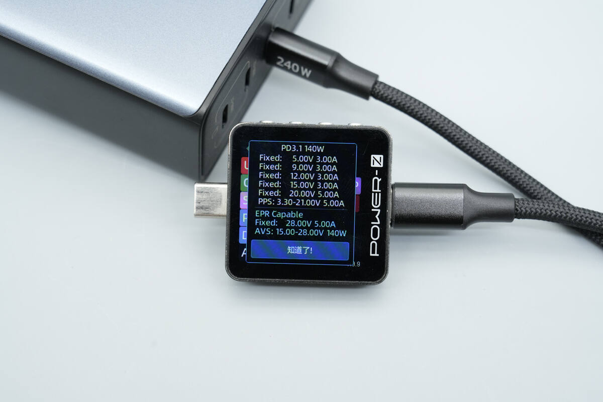
The PDO profiles are also identical.
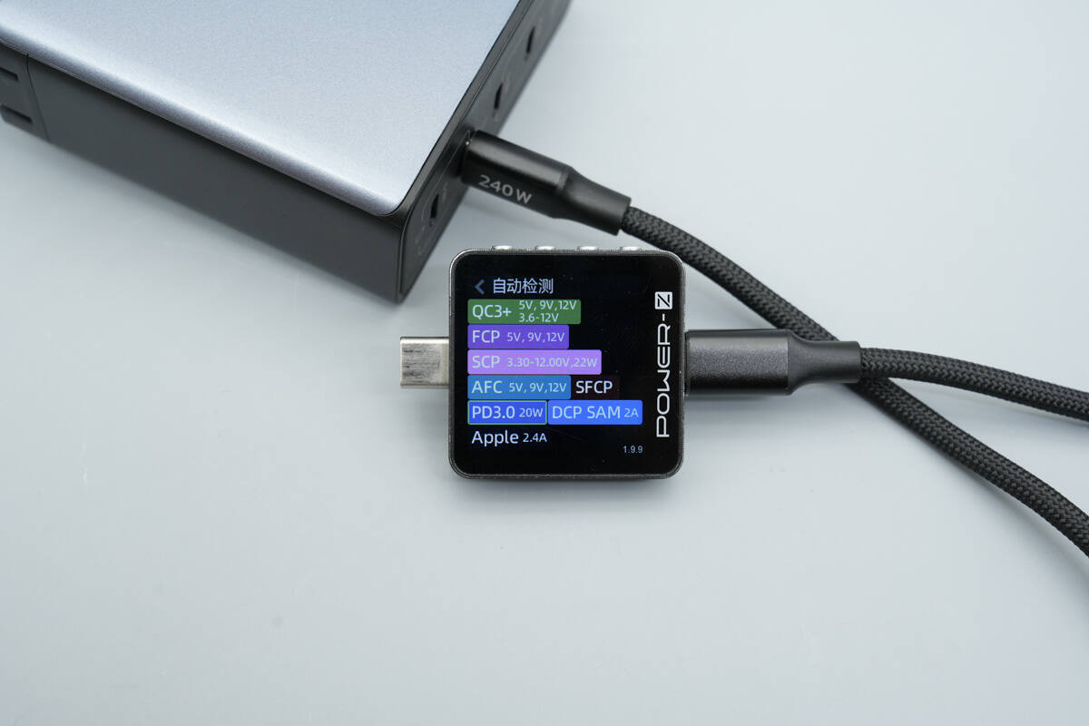
The USB-C2 supports QC3+, FCP, SCP, AFC, SFCP, PD3.0, DCP, SAM 2A, and Apple 2.4A protocols.
It has three fixed PDOs of 5V3A, 9V2.22A, and 12V1.67A.
The USB-C2 port supports the same protocols as the USB-C1 port.
The PDO profiles are also identical.
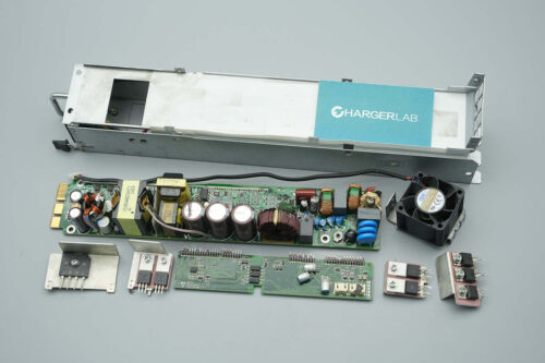
Teardown
Next, let's take it apart to see its internal components and structure.
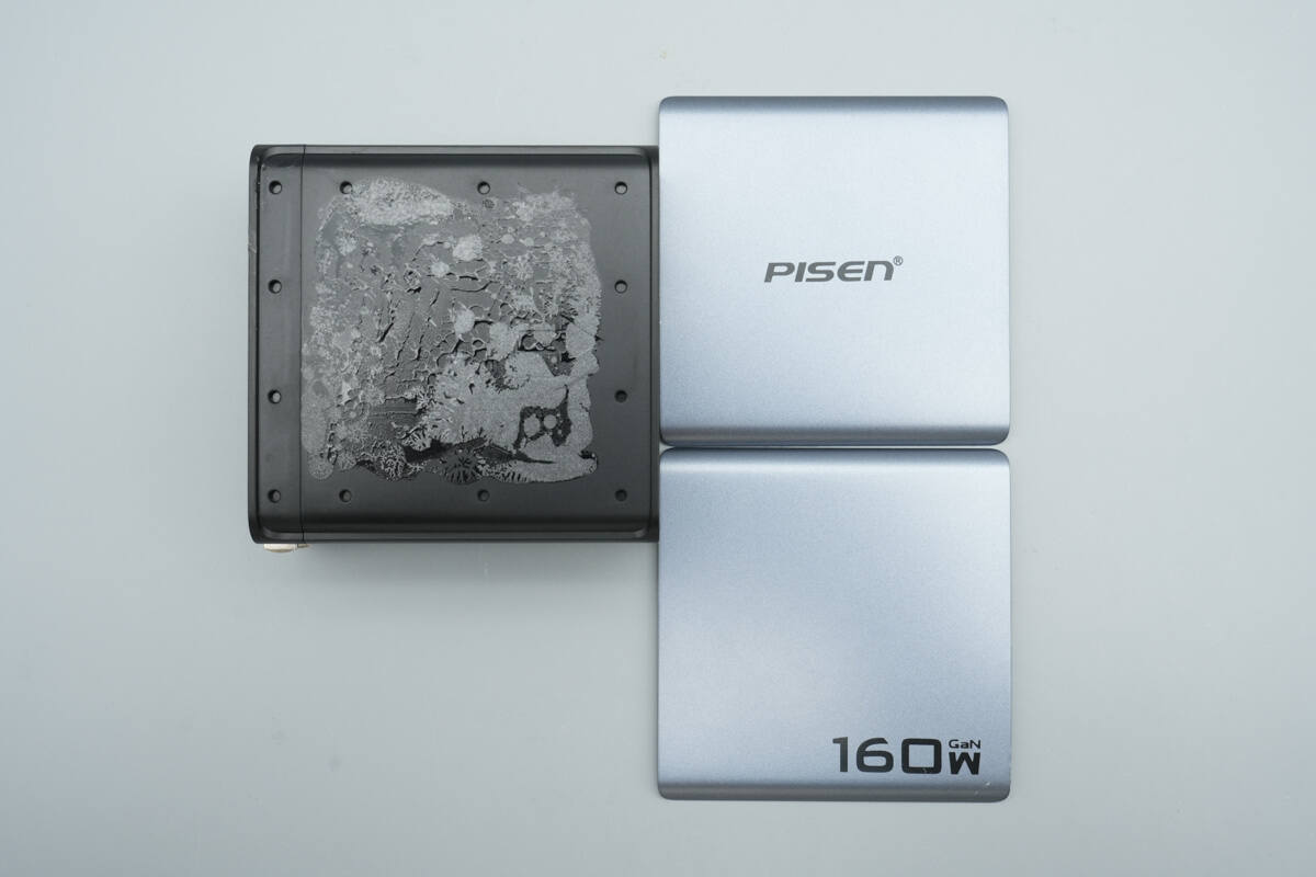
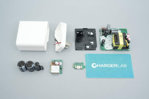
Remove the front and back panels, which are secured with mounting posts and double-sided adhesive.
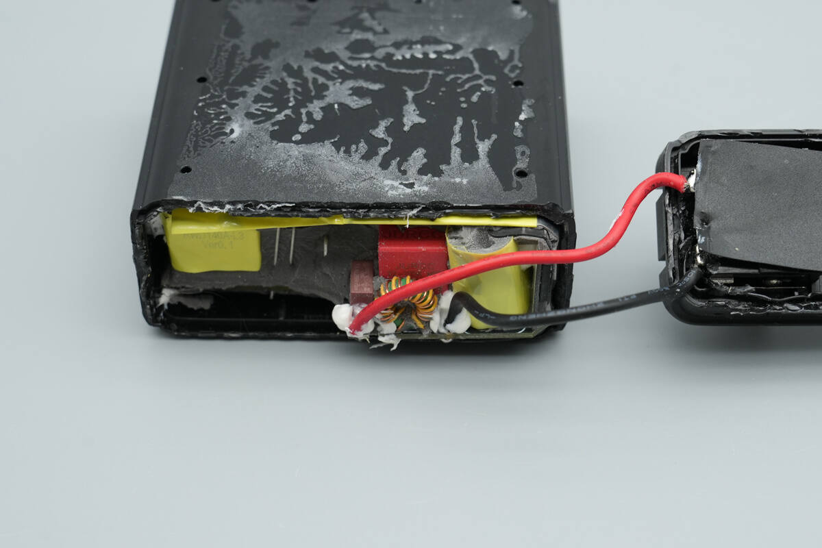
Cut open the input housing, revealing that the plug pins are connected to the PCBA module via wires, with a Mylar sheet applied at the plug area for insulation.
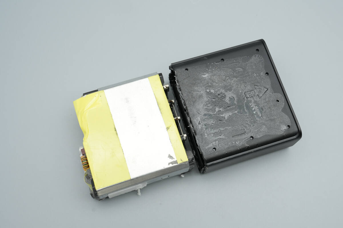
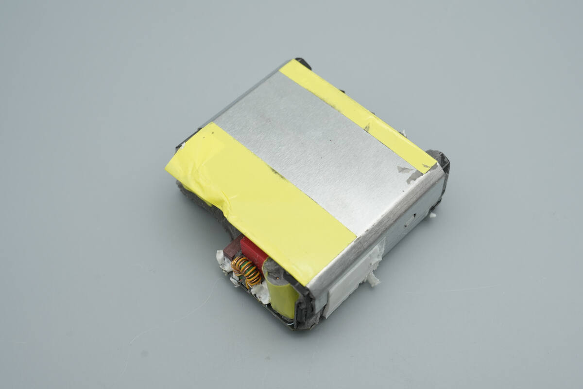
Remove the PCBA module.
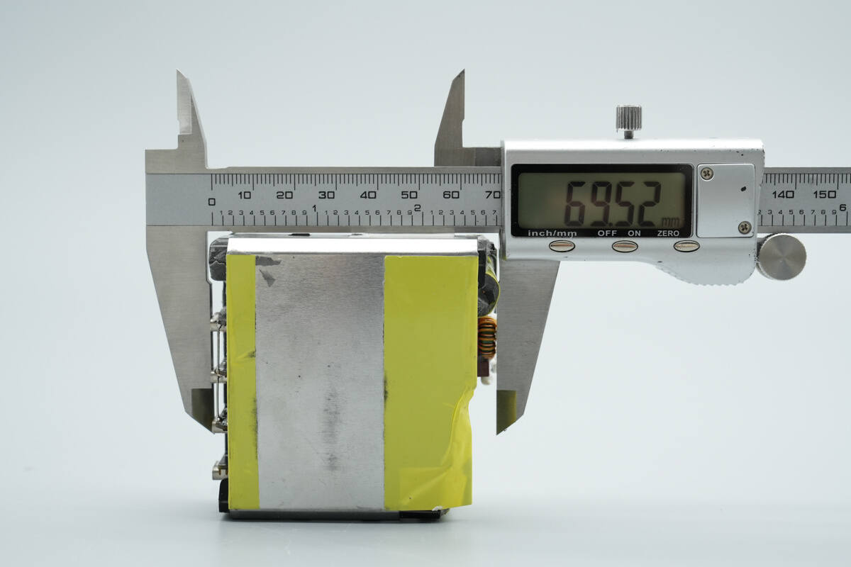
The length of the PCBA module is about 69.52 mm (2.74 inches).
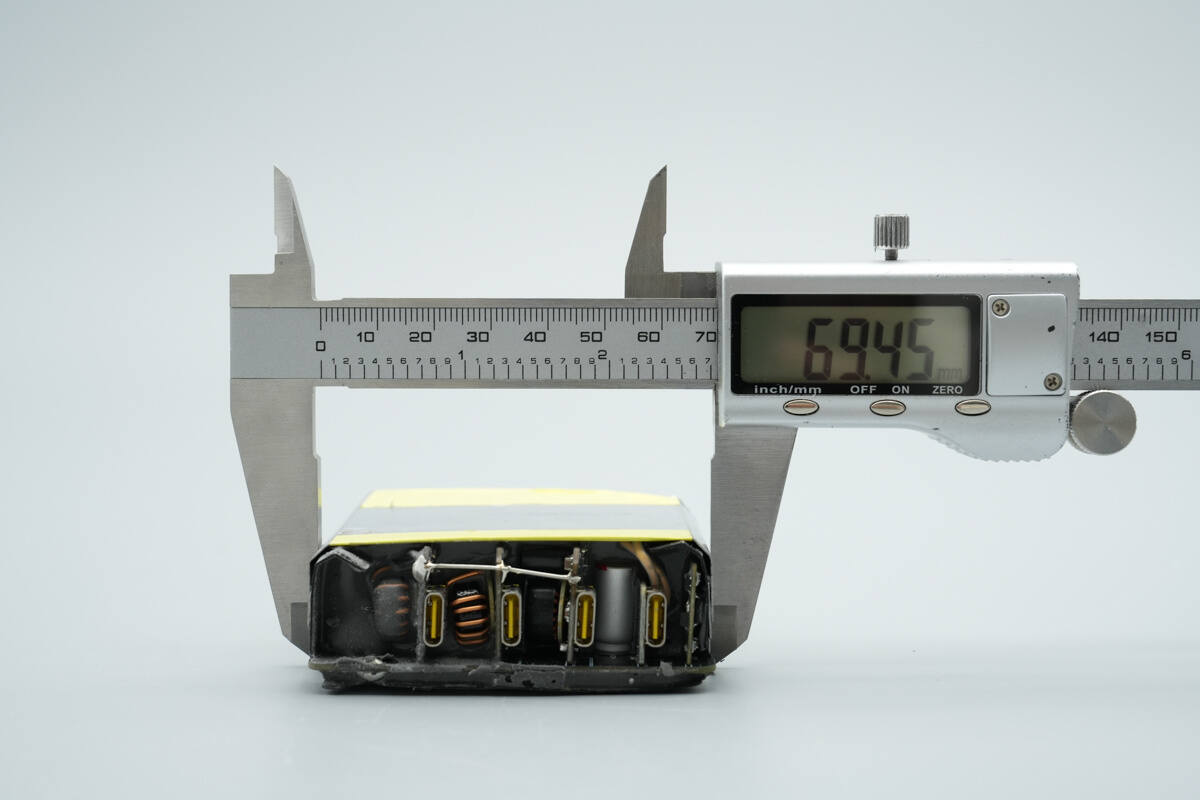
The width is about 69.45 mm (2.73 inches).
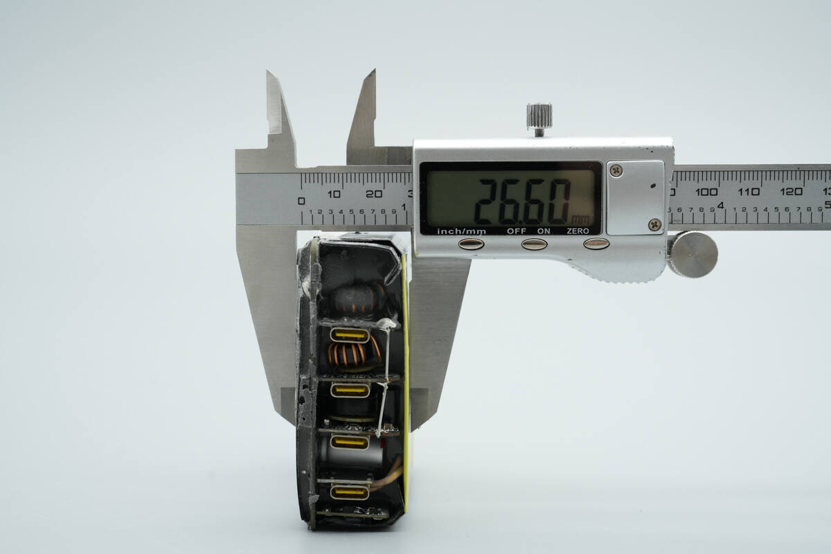
The thickness is about 26.6 mm (1.047 inches).
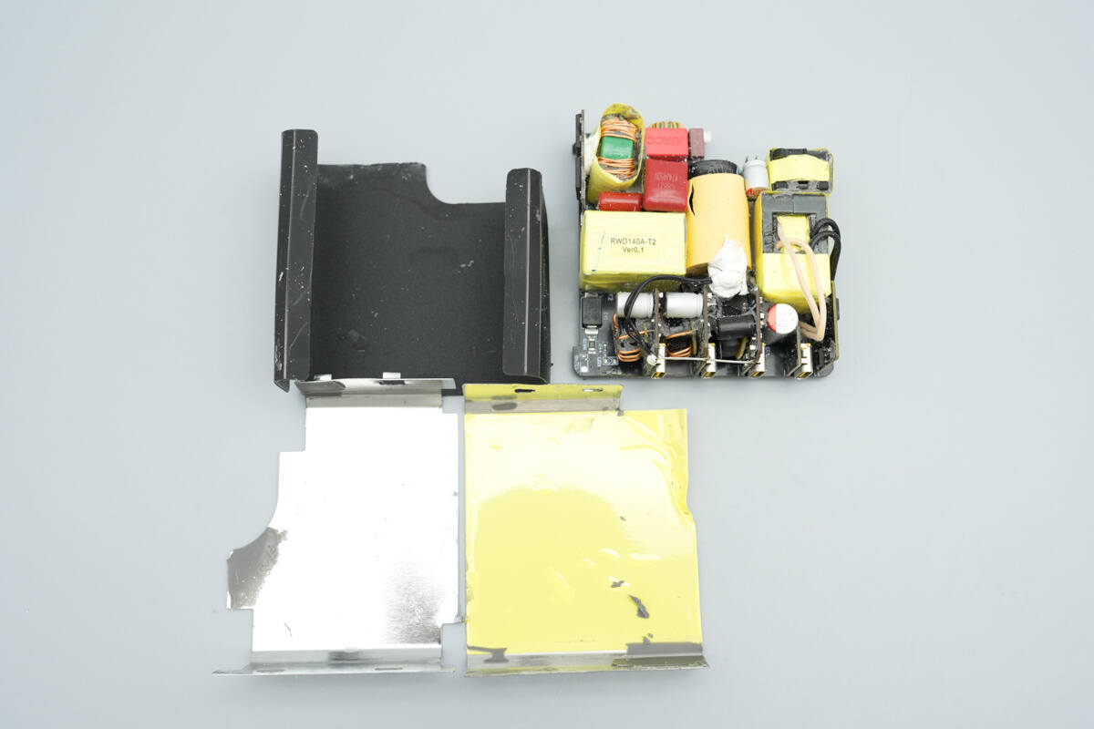
The top of the PCBA module is covered by a heatsink, with insulating tape applied at both ends of the heatsink.
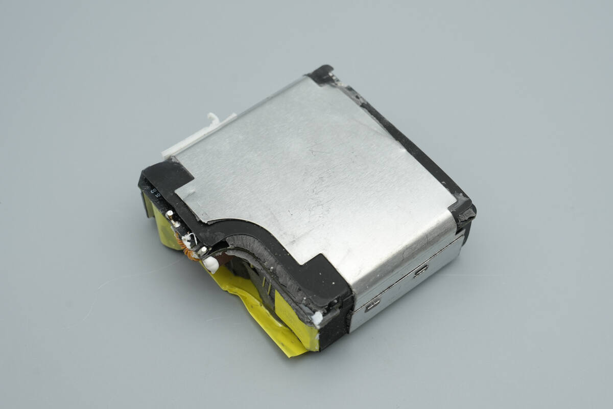
The bottom is also covered by a heatsink, with a Mylar sheet placed on the inner side.
Remove the heatsinks, revealing that the inner side of the top heatsink is lined with insulating tape.
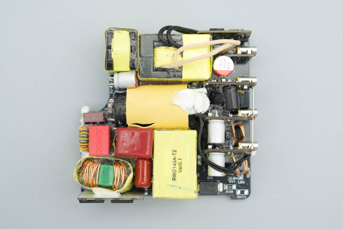
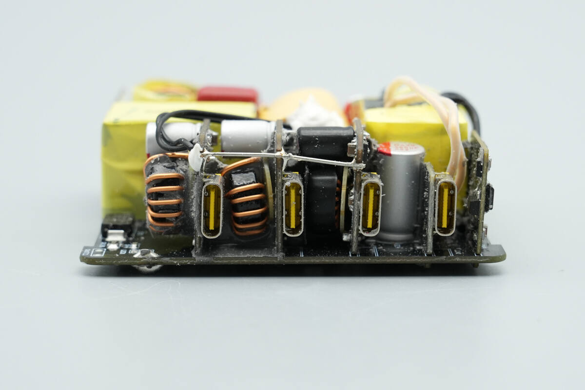
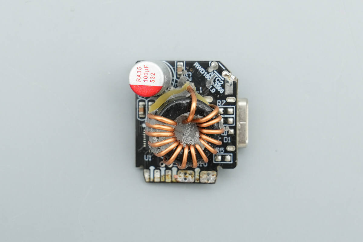
The components on the front of the PCBA module are arranged compactly, with electrolytic capacitors placed in the central area and secured with adhesive.
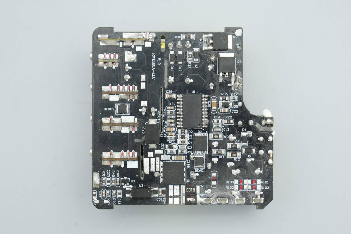
The back side houses the master control chip, PFC MOSFETs, PFC rectifier, LLC MOSFETs, and an optocoupler, among other components.
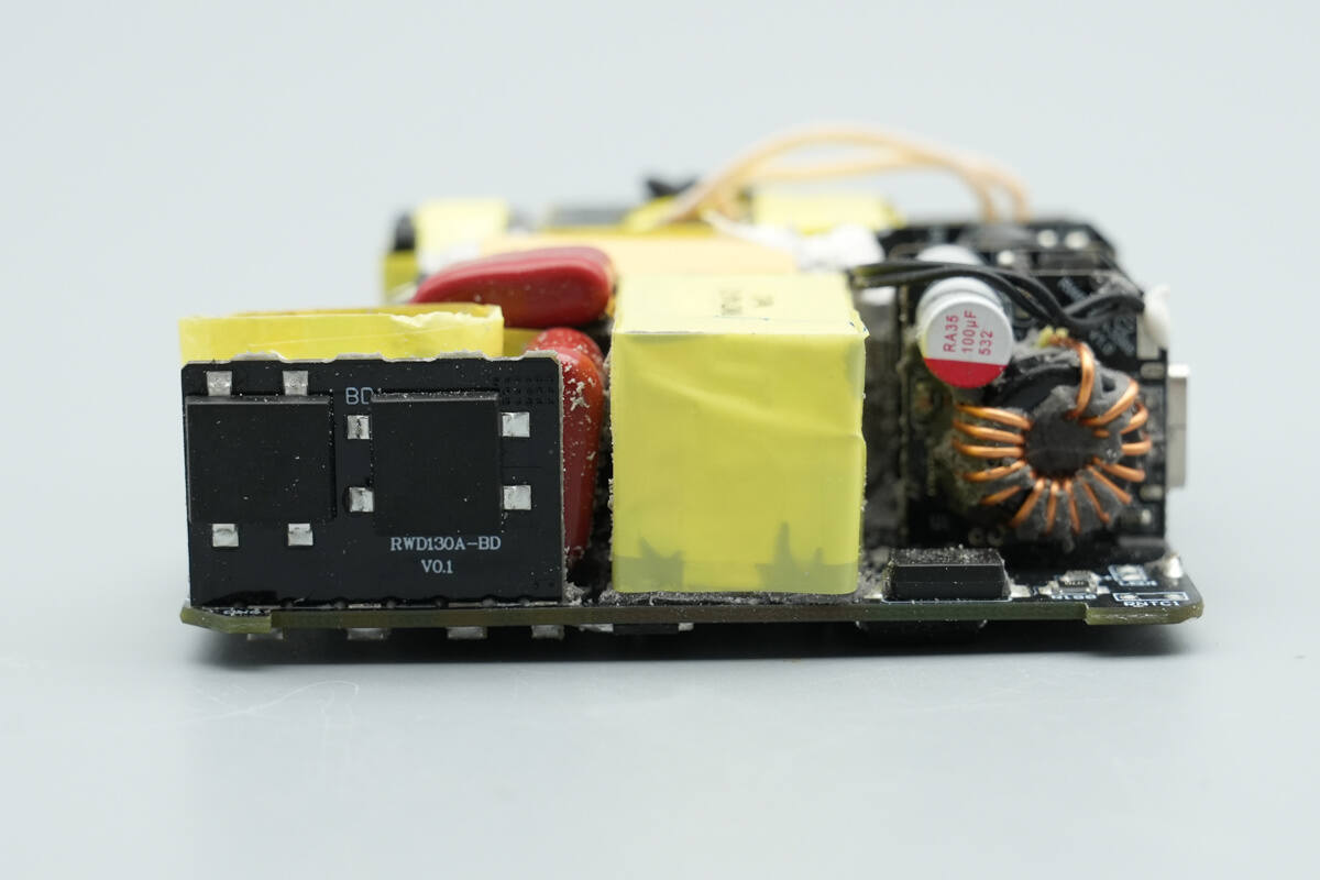
A rectifier PCB is soldered on this side of the module, featuring two bridge rectifiers.
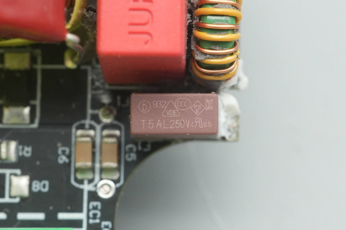
The time-delay fuse is from Betterfuse, part number 932, rated at 5A 250V.
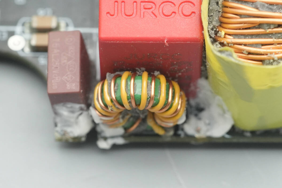
The common mode choke is used to suppress EMI interference.
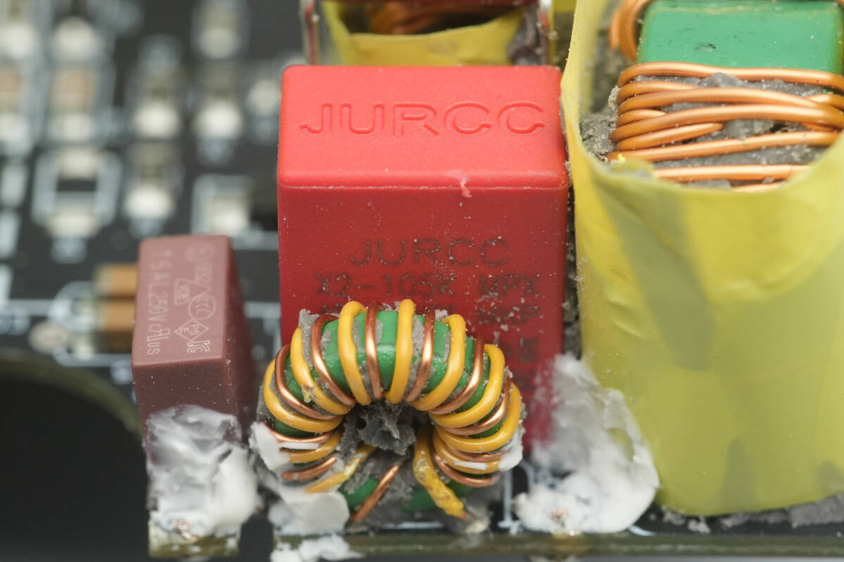
The safety X2 capacitor is from JURCC, with a capacitance of 1 μF.
Another common mode choke is wrapped with insulating tape.
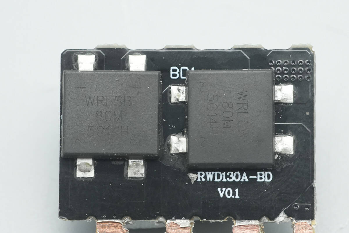
The bridge rectifiers are from World Industrial, model WRLSB80M. This soft-recovery bridge features a gentle turn-off characteristic, which helps minimize diode junction capacitance and reduce harmonic oscillations. The chosen LSB package offers good thermal performance, enhancing reliability for medium- to high-wattage adapters, with each diode capable of handling over 60W.

The film capacitor is from TQCAP, rated at 1 μF 450V.
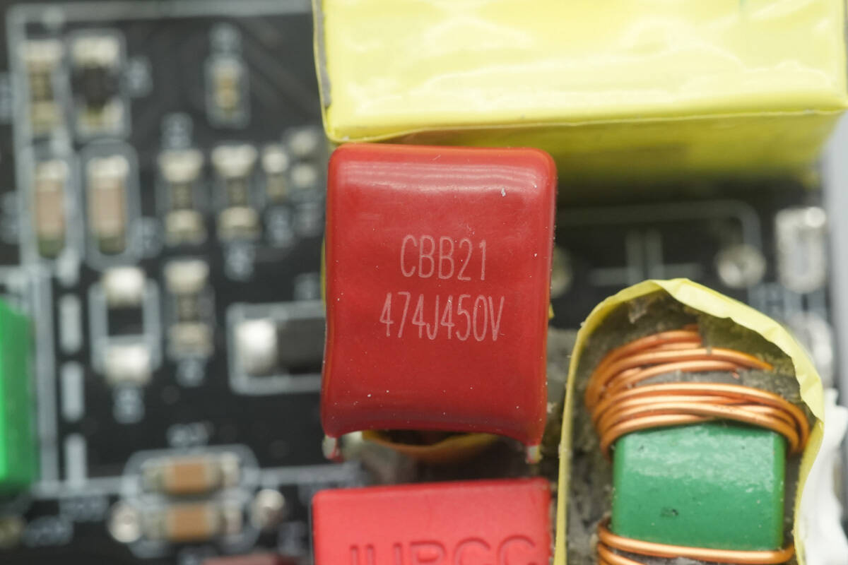
Another CBB21 film capacitor is rated at 0.47 μF 450V.
The filter inductor is also wrapped with insulating tape.

The master control chip is an MPS HR1211, a multi-mode PFC and current-mode LLC dual-function controller. It integrates functions that would normally require 2–3 separate chips into a single IC. The PFC controller supports both CCM and DCM operating modes.
The HR1211 uses a digital control core, supports high-voltage startup and intelligent X-capacitor discharge, and can operate the PFC stage at up to 250 kHz. The LLC stage features a built-in 600 V half-bridge driver with an integrated bootstrap diode, operating at frequencies up to 500 kHz. It also provides comprehensive protection functions and comes in an SOIC-20 package.
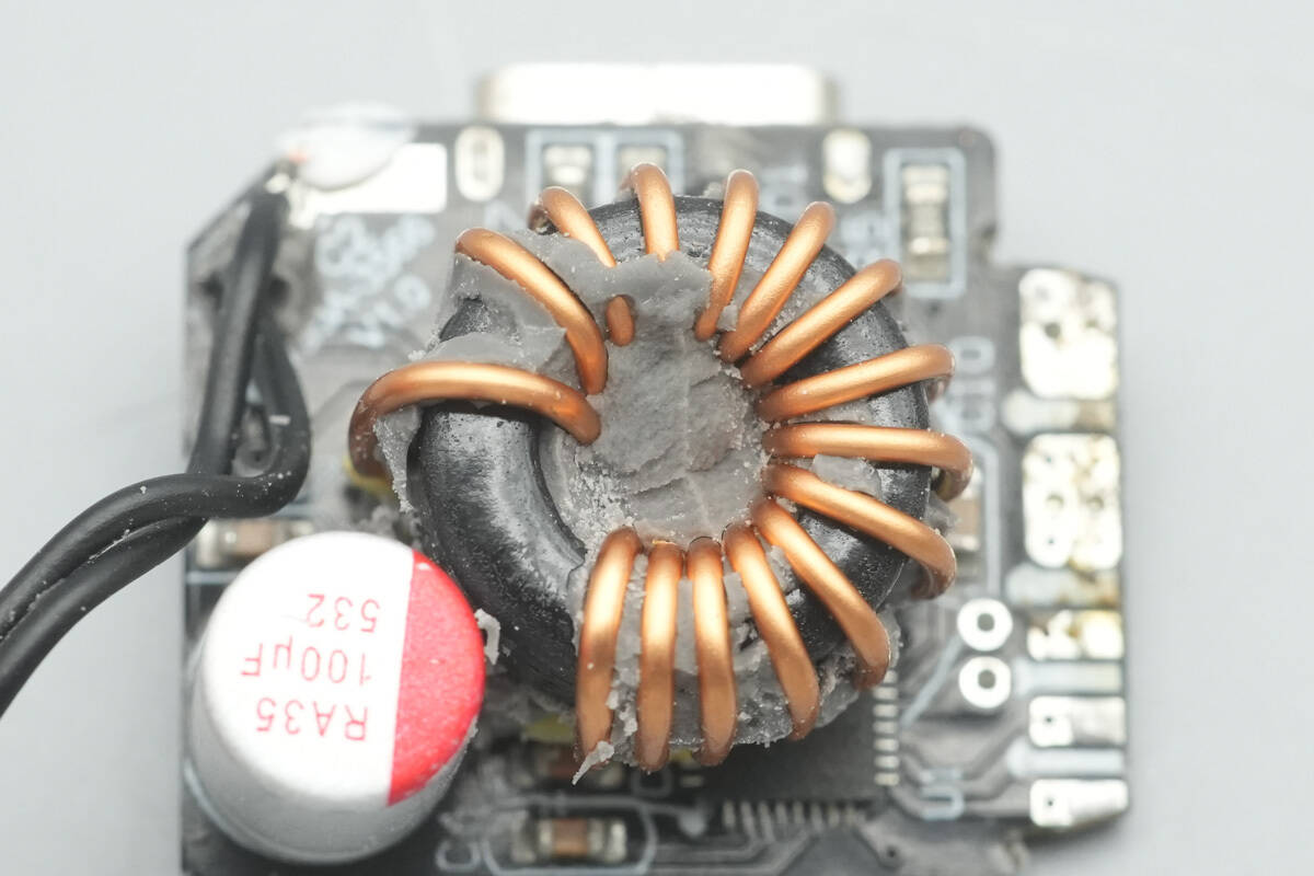
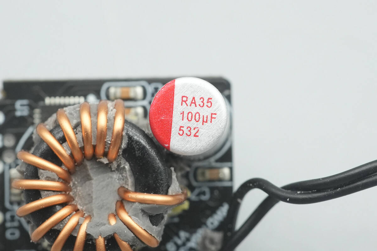
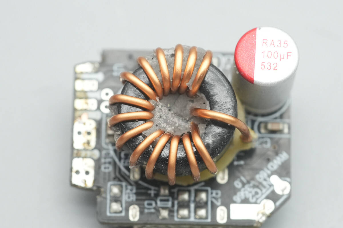
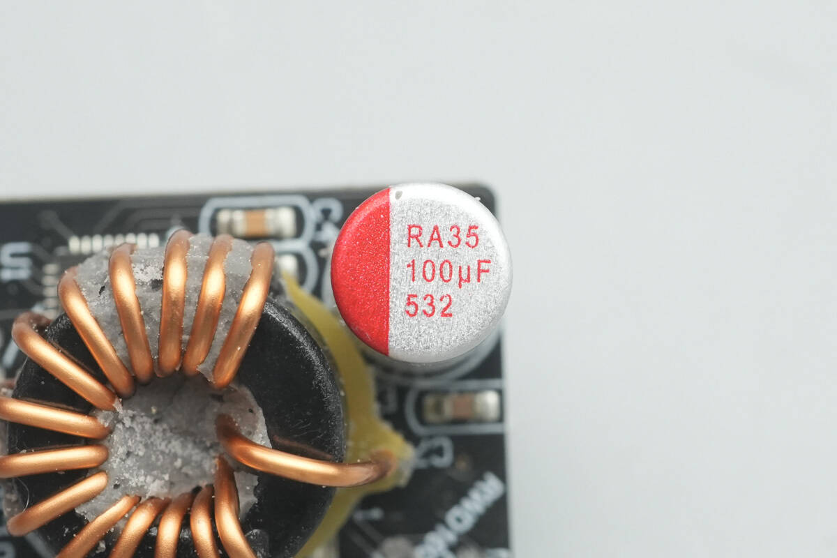
The capacitor supplying power to the master control chip is rated at 35 V 100 μF.
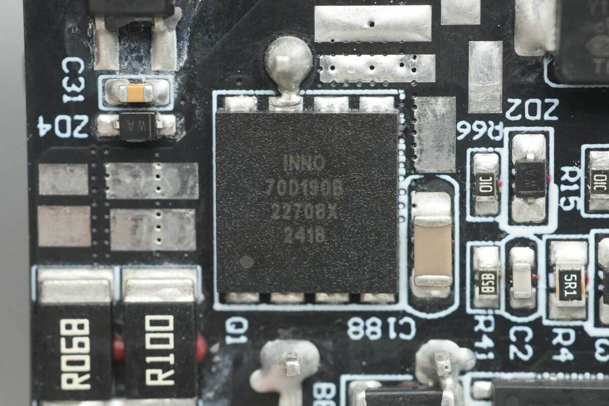
The PFC MOSFET is an Innoscience INN700DA190B, a 700 V enhancement-mode GaN transistor. Compared to the previous 650 V rating, it has been upgraded to 700 V with a transient voltage tolerance of 800 V. The device has an on-resistance of 190 mΩ, supporting higher-power applications.
The Innoscience INN700DA190B supports ultra-high switching frequencies, has no reverse-recovery charge, and features very low gate and output charge. It meets JEDEC industrial standards, includes built-in ESD protection, and complies with RoHS, lead-free, and EU REACH regulations. It is suitable for high-efficiency, high-density applications such as AC–DC and DC–DC conversion, and comes in a DFN 5×6 package.
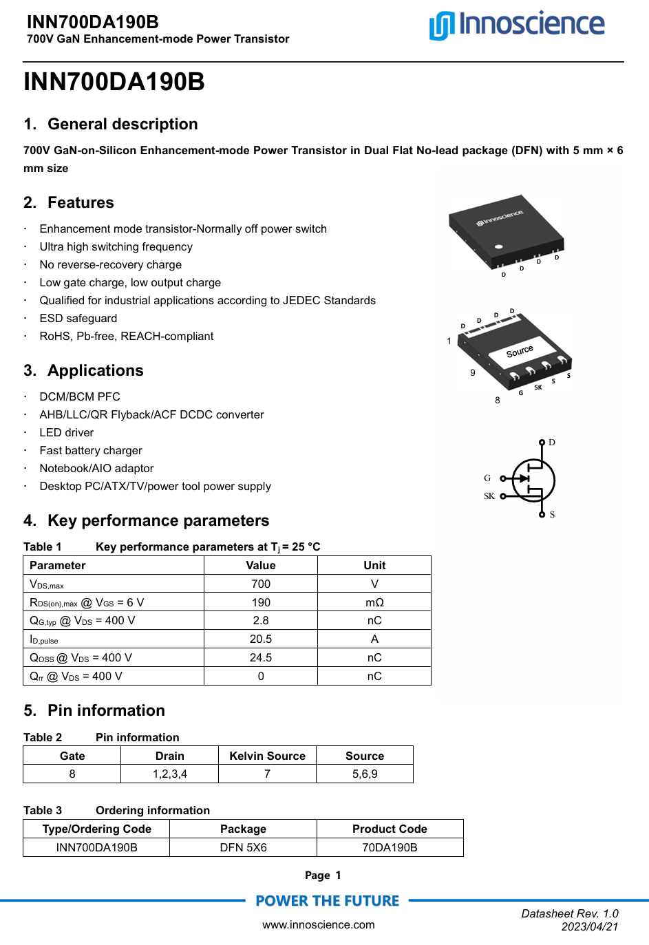
Here is the information about Innoscience INN700DA190B.
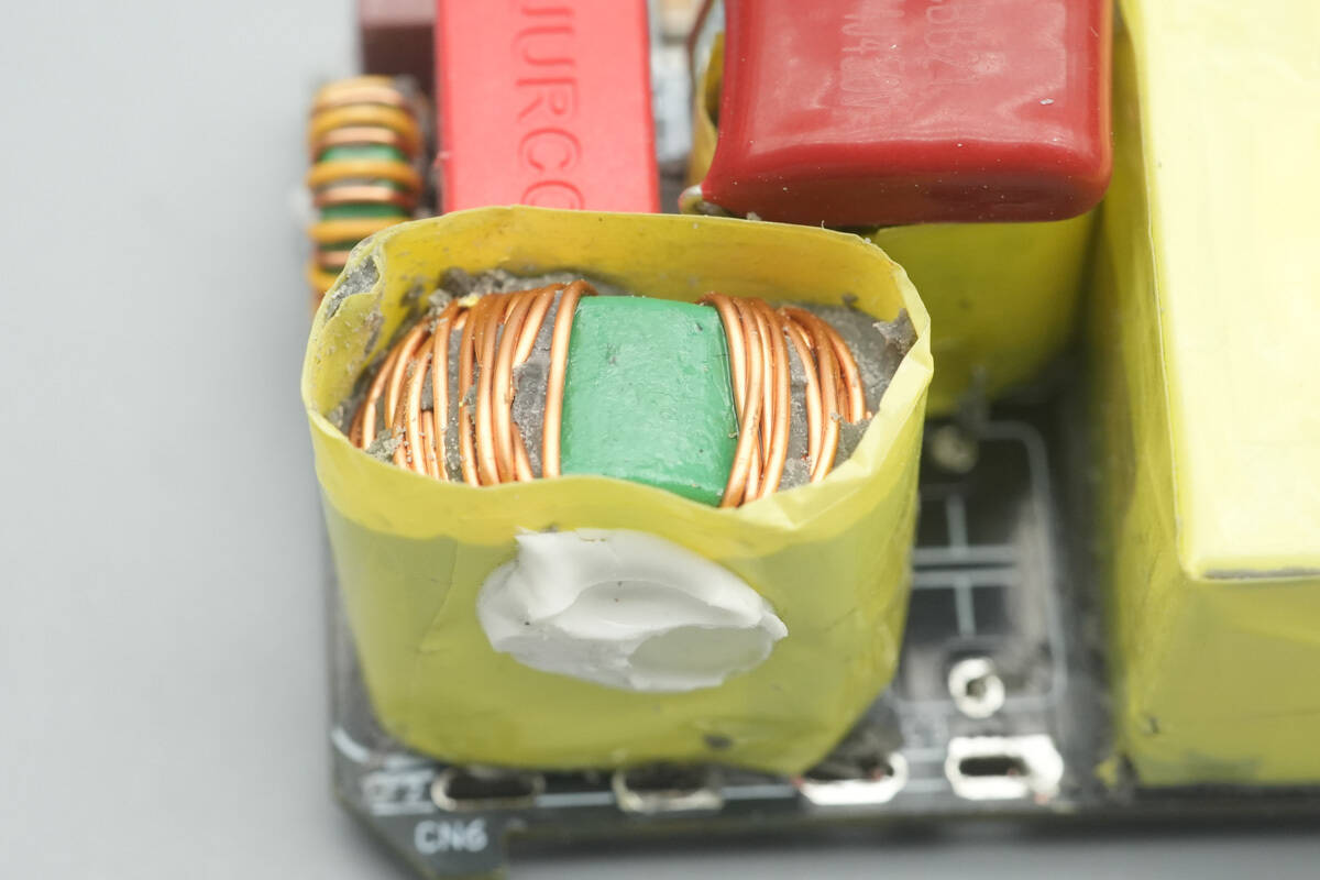
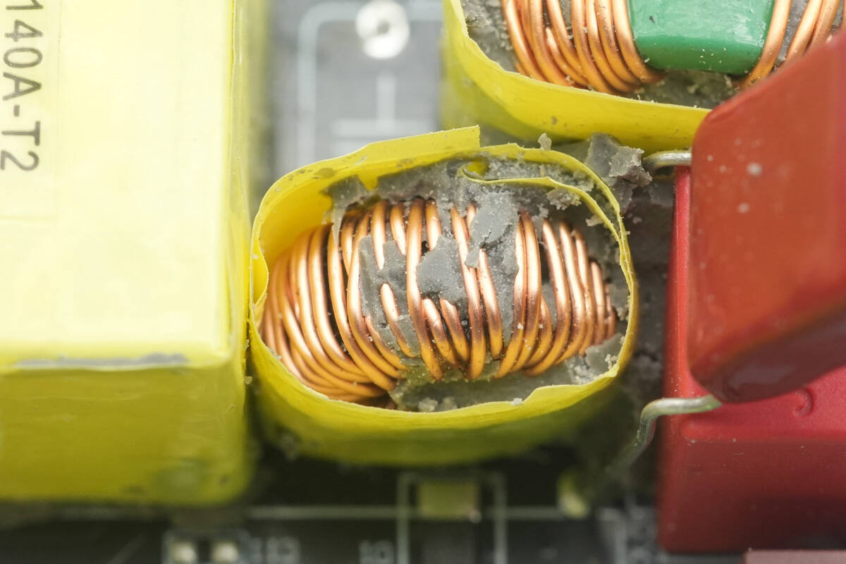
Close-up of the PFC boost inductor.
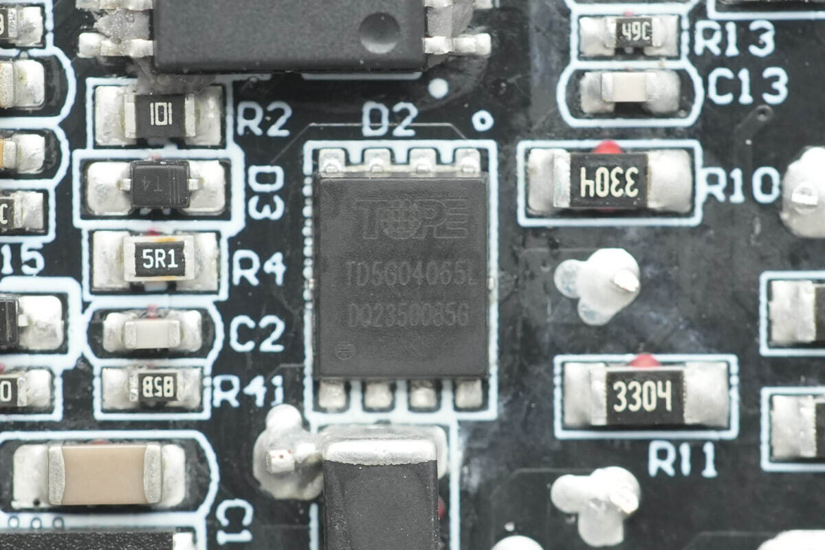
The PFC rectifier is a TOPE TD5G04065L, a 650 V silicon carbide Schottky diode, housed in a DFN 5×6 package.
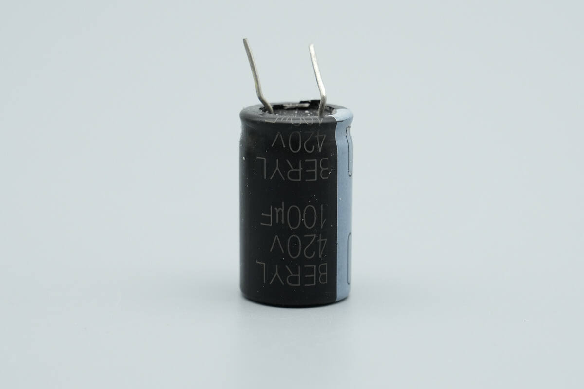
The high-voltage filter electrolytic capacitor is from BERYL, rated at 420 V 100 μF.
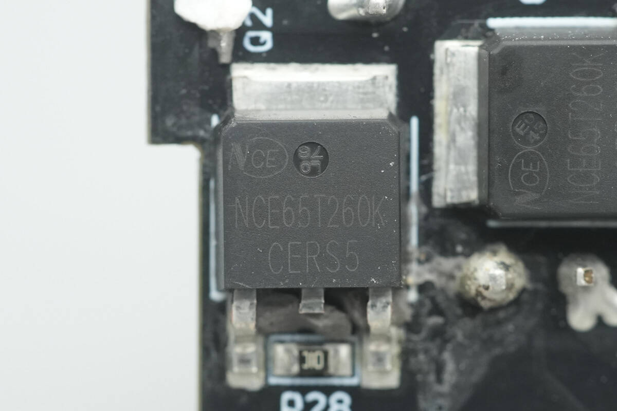
The two LLC MOSFETs are NCEPower NCE65T260K, NMOS devices rated at 600 V with an on-resistance of 220 mΩ, packaged in TO-252.
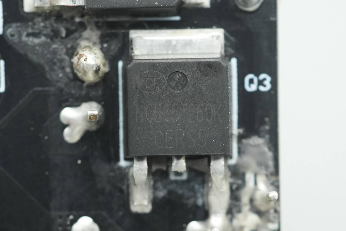
Close-up of the other LLC MOSFET.

Close-up of the resonant inductor.
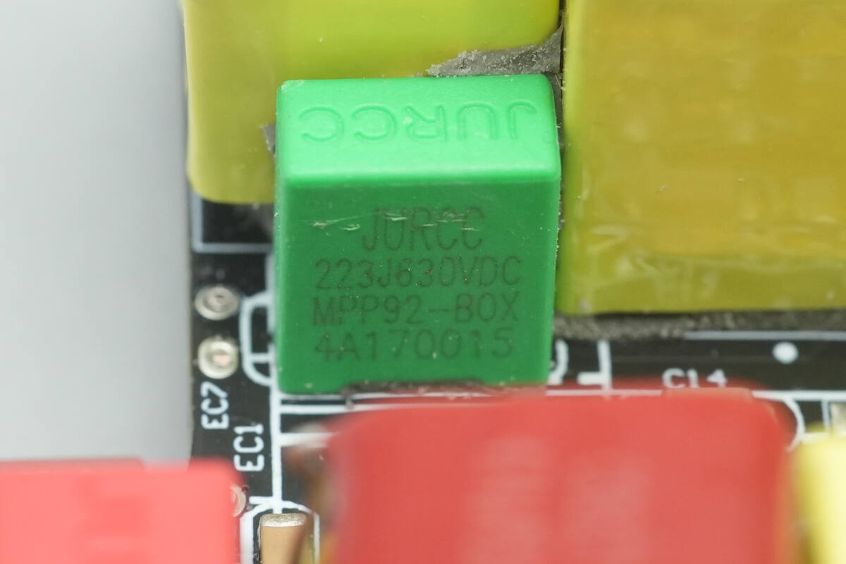
The resonant capacitor is also from JURCC, rated at 0.022 μF 630 V.
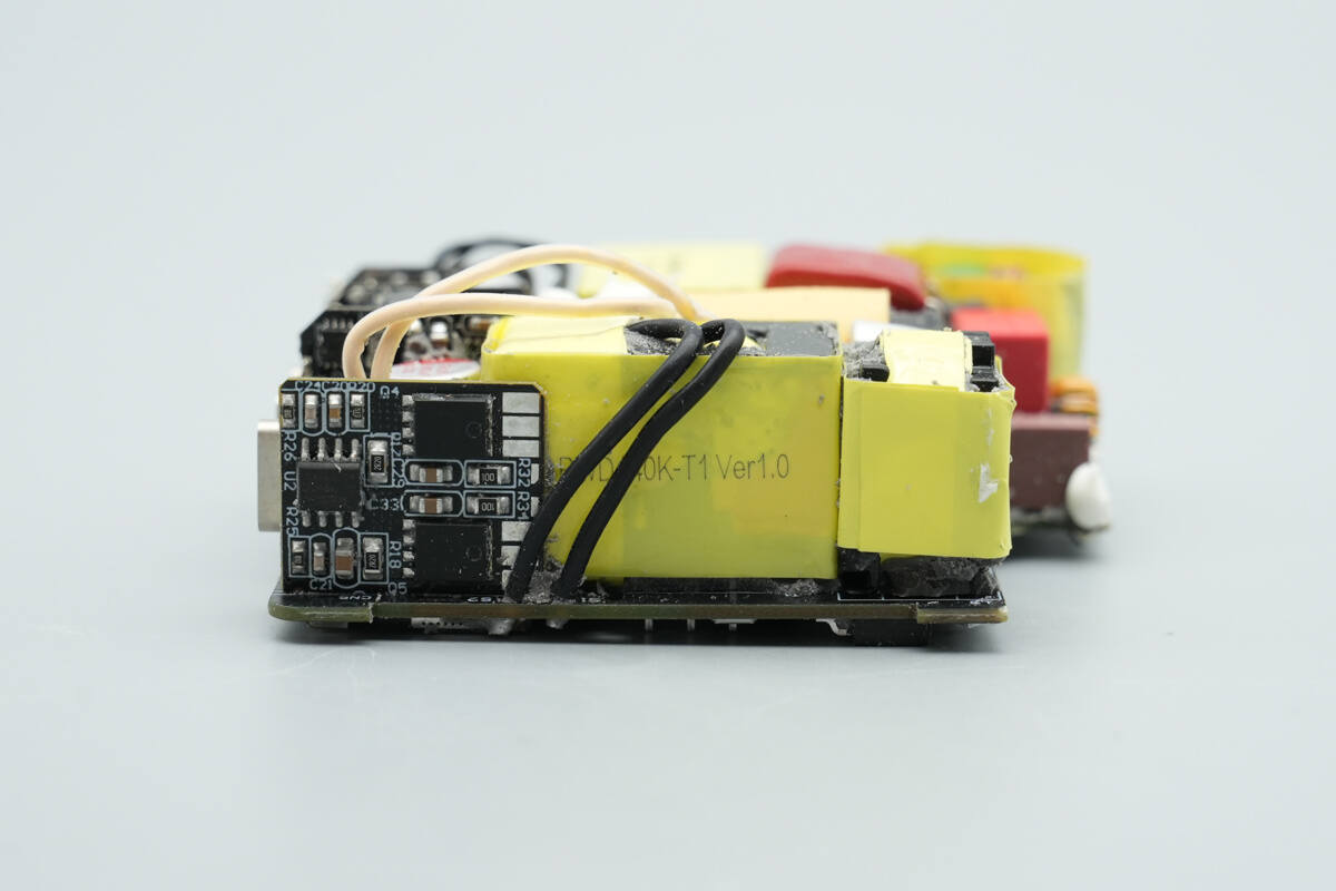
On the other side of the module, there is a transformer and a synchronous rectifier PCB. The front of the PCB houses the synchronous rectifier controller and the synchronous rectifiers.
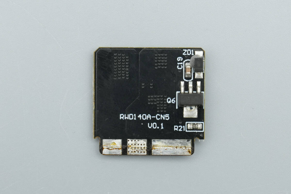
Remove the small PCB, revealing the transistor on the back side.
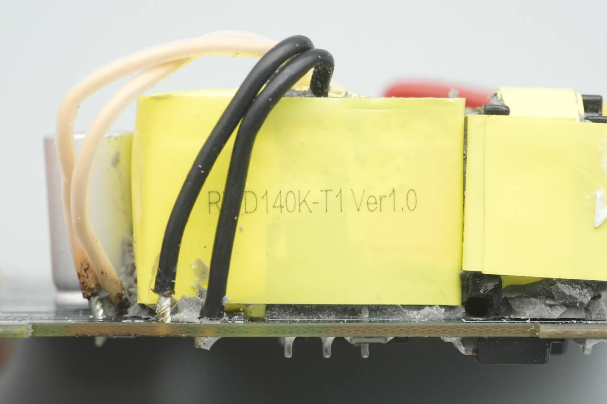
Close-up of the transformer.
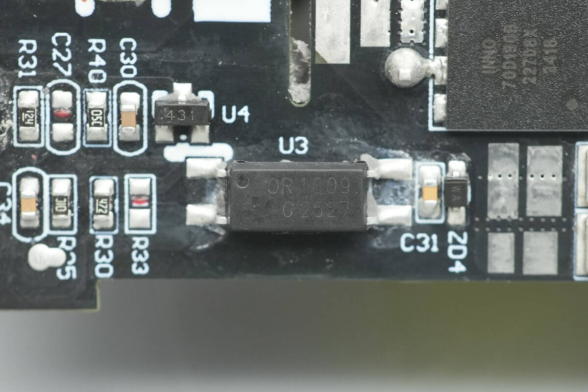
The OR1009 optocoupler is used for output voltage feedback.
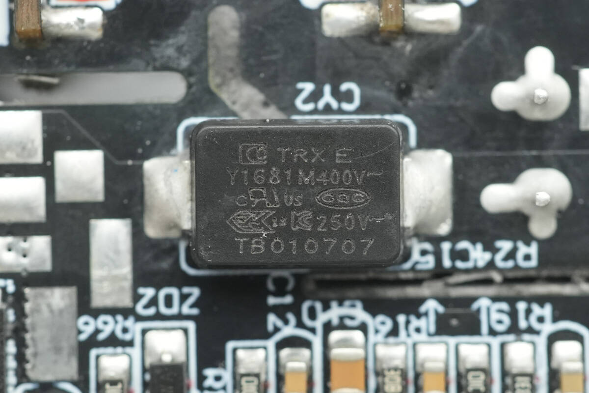
The SMD Y capacitor is from TRX, part number TMY1681M. Its compact size and light weight make it well-suited for high-density power products such as GaN fast chargers.
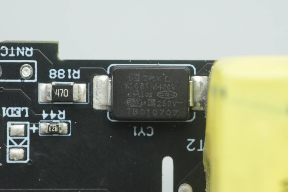
Another SMD Y capacitor has the same part number.
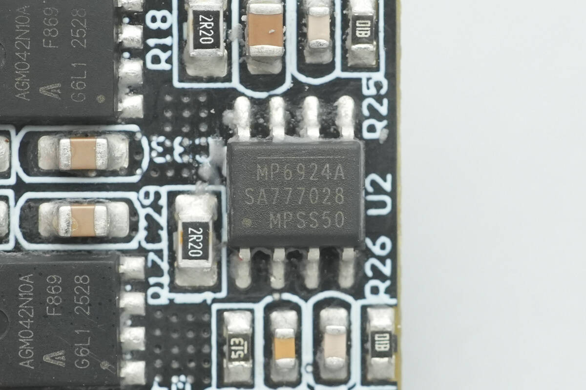
The LLC synchronous rectifier controller is an MPS MP6924A, offering enhanced noise immunity and fast turn-off capability, and is compatible with both CCM and DCM modes. The MP6924A integrates two synchronous rectifier controllers internally, each used for rectifying the outputs of the two secondary coils in an LLC converter. It is suitable for LLC converter synchronous rectification applications and comes in an SOIC-8 package.
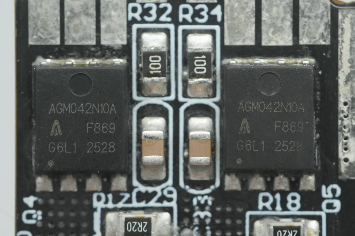
The two synchronous rectifiers are AGM-Semi AGM042N10A, 100 V NMOS devices with an on-resistance of 4.2 mΩ, packaged in PDFN 5×6.
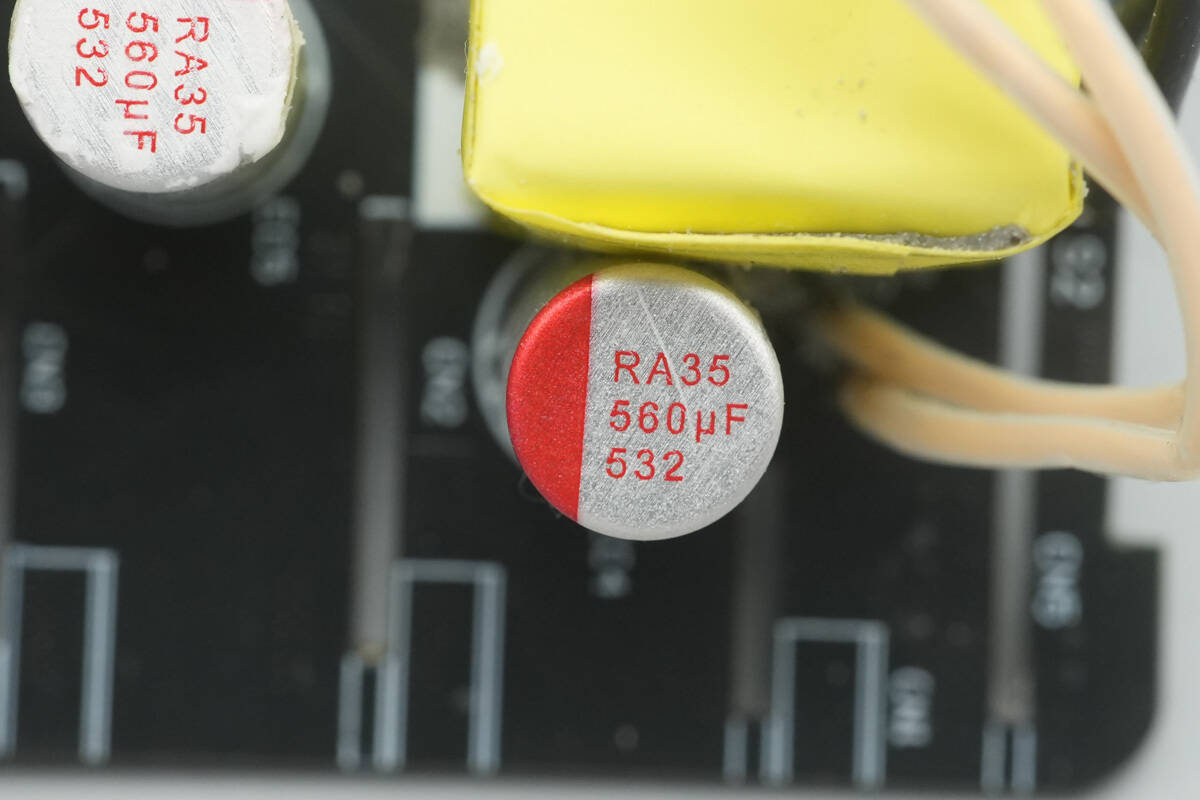
The solid capacitor used for output filtering is rated at 35 V 560 μF.
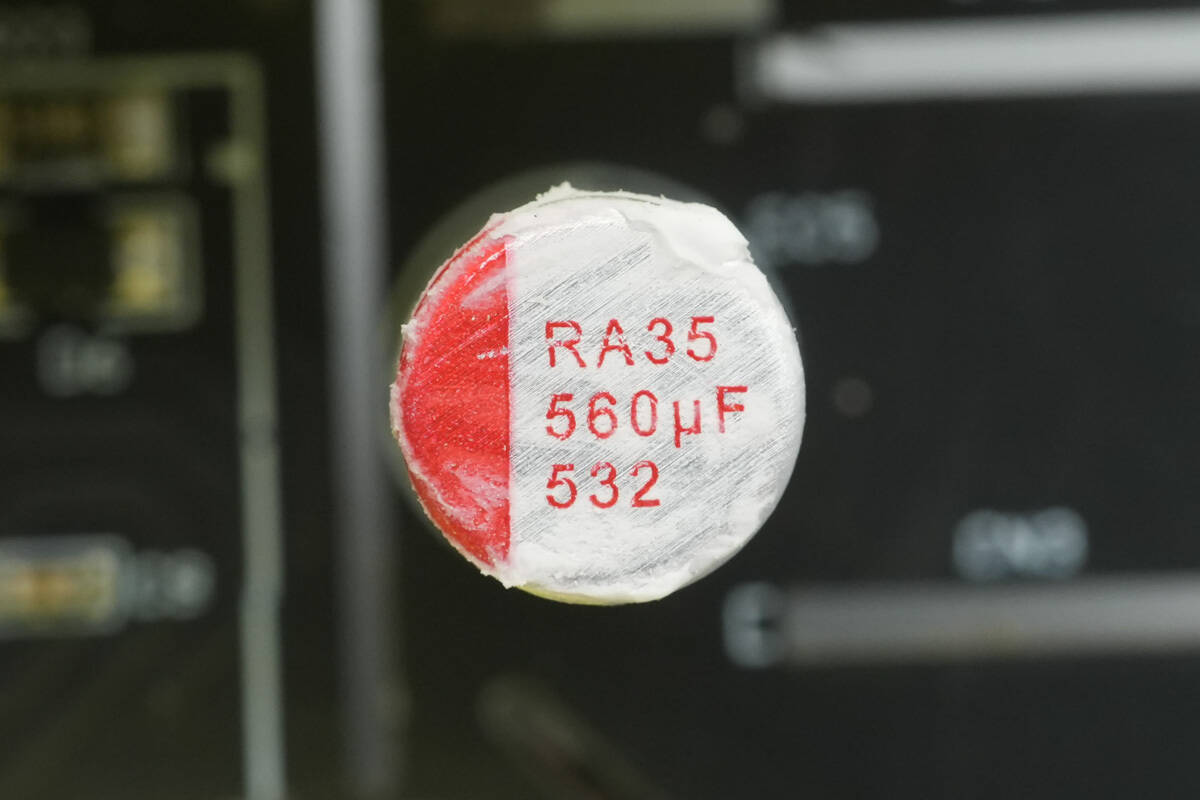
Another solid capacitor with the same specifications is also used.
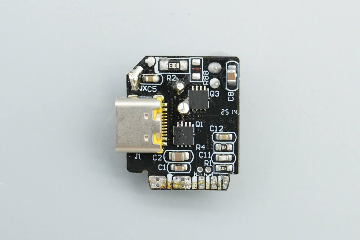
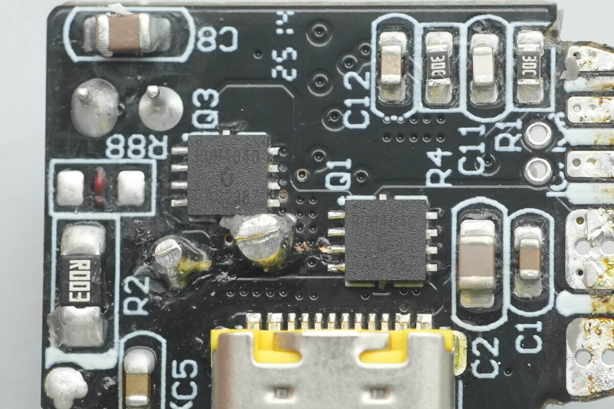
All four USB-C sockets are soldered onto separate small PCBs.
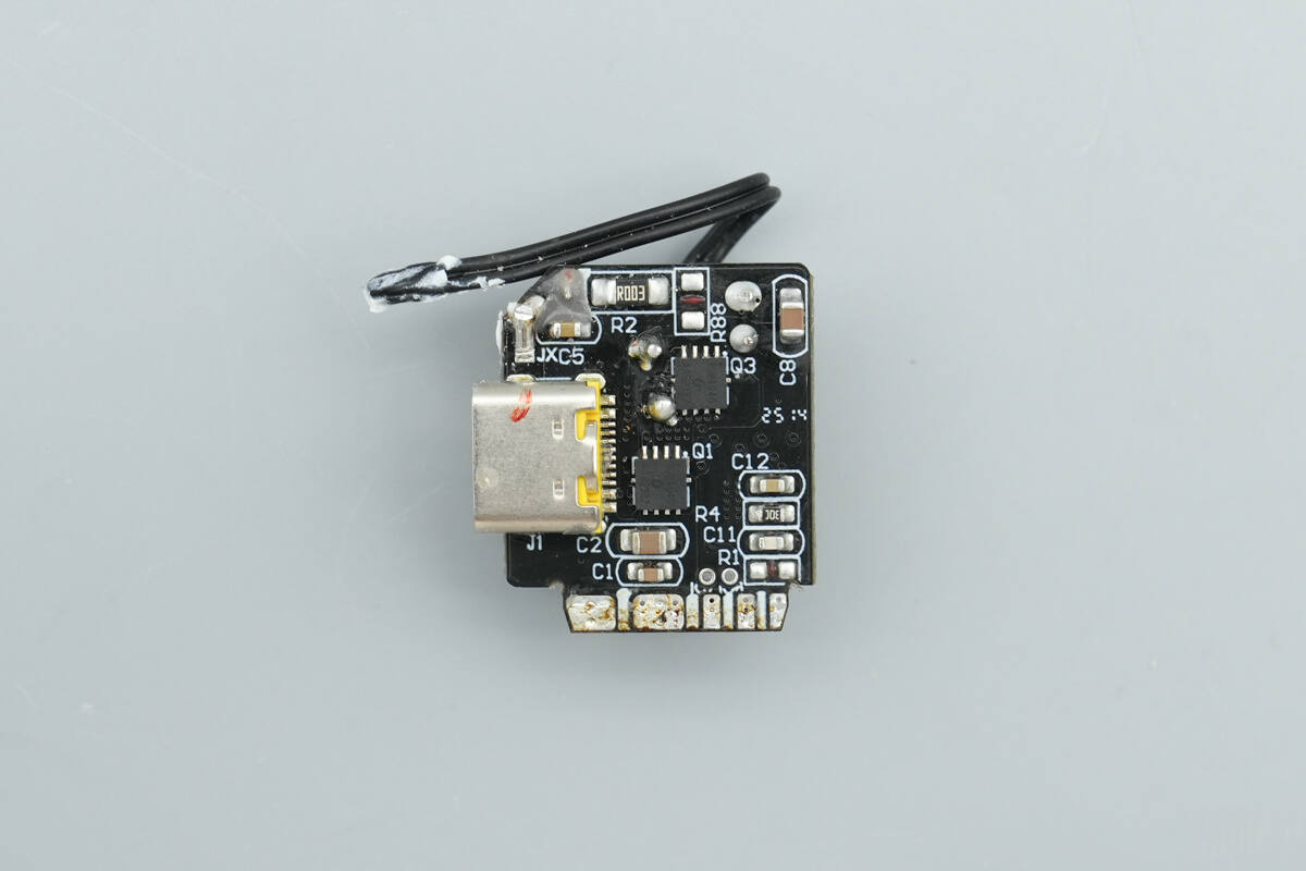
The small PCB for the USB-C4 socket has two synchronous buck MOSFETs on the front side.
On the back side, there is a buck protocol chip, a buck inductor, a solid capacitor, and a thermistor.
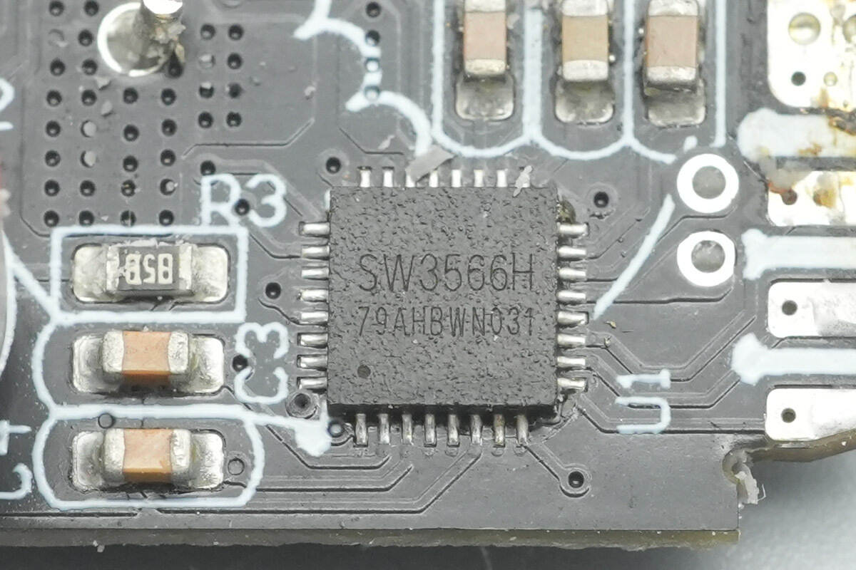
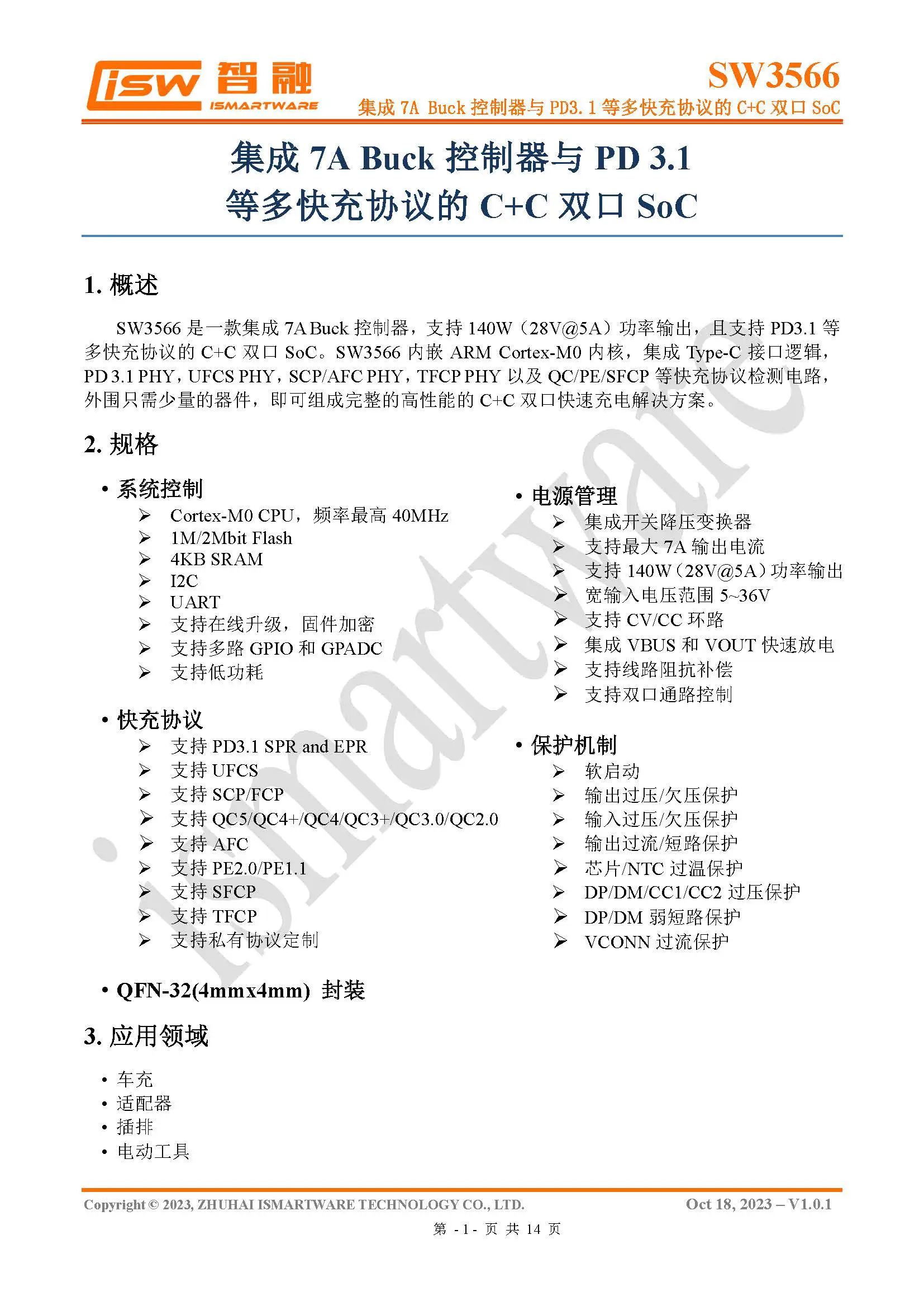
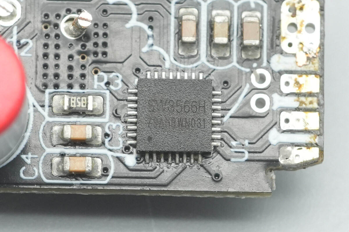
The USB-C4 buck protocol chip is an iSmartWare SW3566H, a highly integrated dual-port fast-charging IC that supports both USB-C and USB-A charging, with independent current limiting for each port. It integrates a high-efficiency synchronous buck converter, supporting 20V 7A and 28V 5A outputs, and is compatible with PD 3.1, QC, SCP, UFCS, and other fast-charging protocols. It also allows custom fast-charging protocol support, with a maximum output power of 140W.
The SW3566H integrates CC/CV modes, dual-port management logic, and bus voltage detection. Paired with the corresponding buck MOSFETs and VBUS switches, it enables dual-port buck output. The built-in buck converter operates at 180 kHz and supports both PWM and PFM modes. Protection thresholds for output current, line loss compensation, and other parameters can be configured via the I²C interface. An internal ADC allows data sampling across nine channels, including input/output voltage, output current, and chip temperature, supporting external MCU monitoring.
The SW3566H supports up to 36 V input and a maximum output current of 7 A. It features soft start, input over-/under-voltage protection, output over/under-voltage protection, output overcurrent/short-circuit protection, DP/DM/CC overvoltage protection, over-temperature protection, external NTC thermistor protection, and power-limiting protection. The chip comes in a QFN 4×4–32 package.
Here is the information about iSmartWare SW3566.
The two synchronous buck MOSFETs are Ruichips RUH4040, NMOS devices rated at 40 V with an on-resistance of 8 mΩ, packaged in PDFN 3×3×3.
Close-up of the buck inductor.
The secondary buck solid capacitor used for output filtering is rated at 35 V 100 μF.
Close-up of the thermistor.
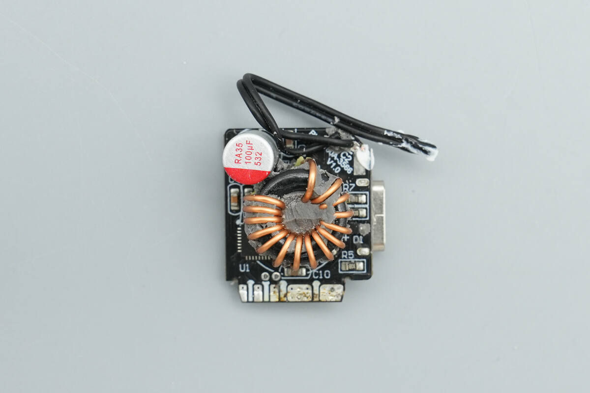
The small PCB for the USB-C3 socket has two synchronous buck MOSFETs on the front side.
On the back side, there is a buck protocol chip, a buck inductor, and a solid capacitor.
The USB-C3 buck protocol chip also uses the iSmartWare SW3566H.
The two synchronous buck MOSFETs are also Ruichips RUH4040.
Close-up of the buck inductor.
The secondary buck solid capacitor used for output filtering is also rated at 35 V 100 μF.
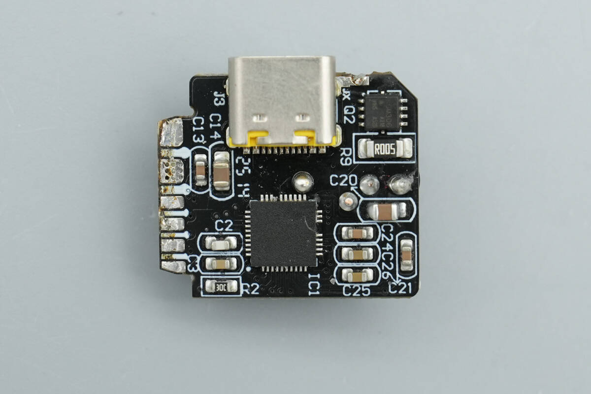
The small PCB for the USB-C2 socket has a buck protocol chip and an output VBUS MOSFET on the front side.
On the back side, there is a buck inductor, a solid capacitor, and an output VBUS MOSFET.
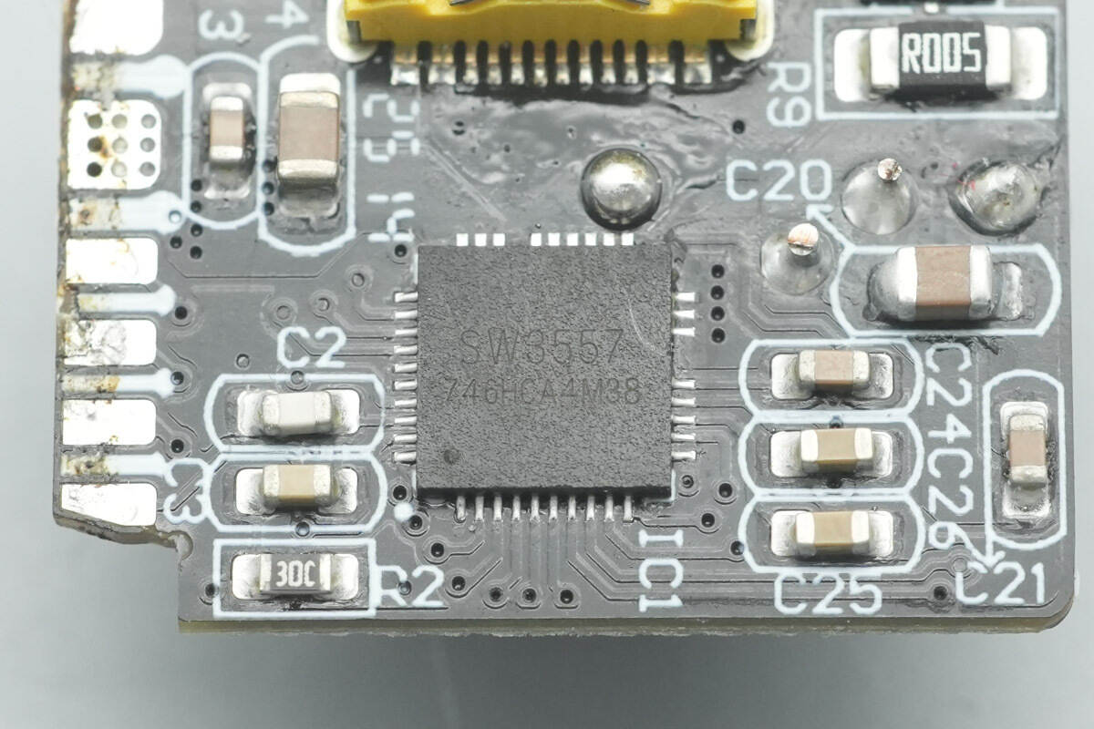
The buck protocol chip for the USB-C1 and USB-C2 ports is iSmartWare SW3557, a highly integrated dual-port fast-charging IC that supports fast charging from either USB-C port with independent current limiting for each port. It is compatible with multiple fast-charging protocols, including PPS, PD, QC, AFC, FCP, SCP, PE, SFCP, and TFCP, with a maximum output power of 65W.
The SW3557 integrates a 5 A high-efficiency synchronous buck converter, CC/CV mode, dual-port management logic, and dual-chip dynamic power allocation. With minimal external components, it forms a complete high-performance dual USB-C fast-charging solution. The chip comes in a QFN 5.5×5.5–37 package.
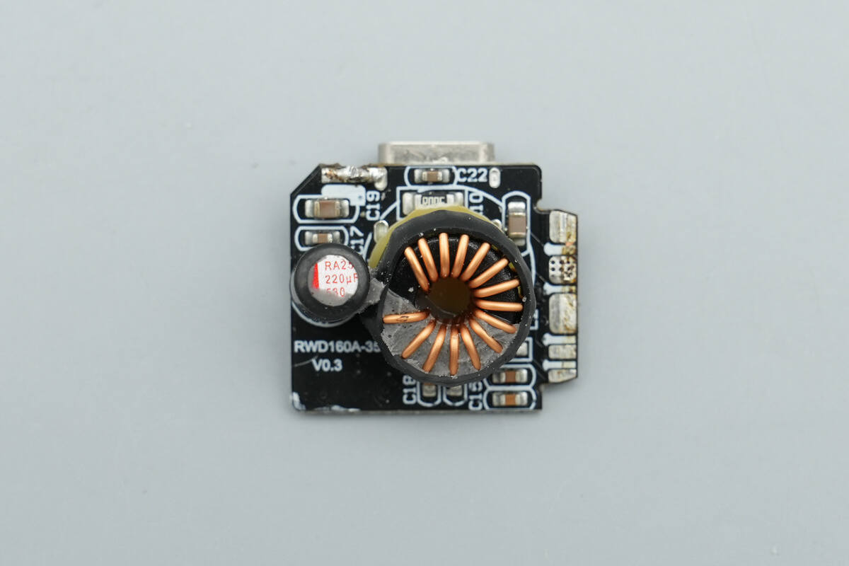
The buck inductor is insulated with a heat-shrink sleeve.
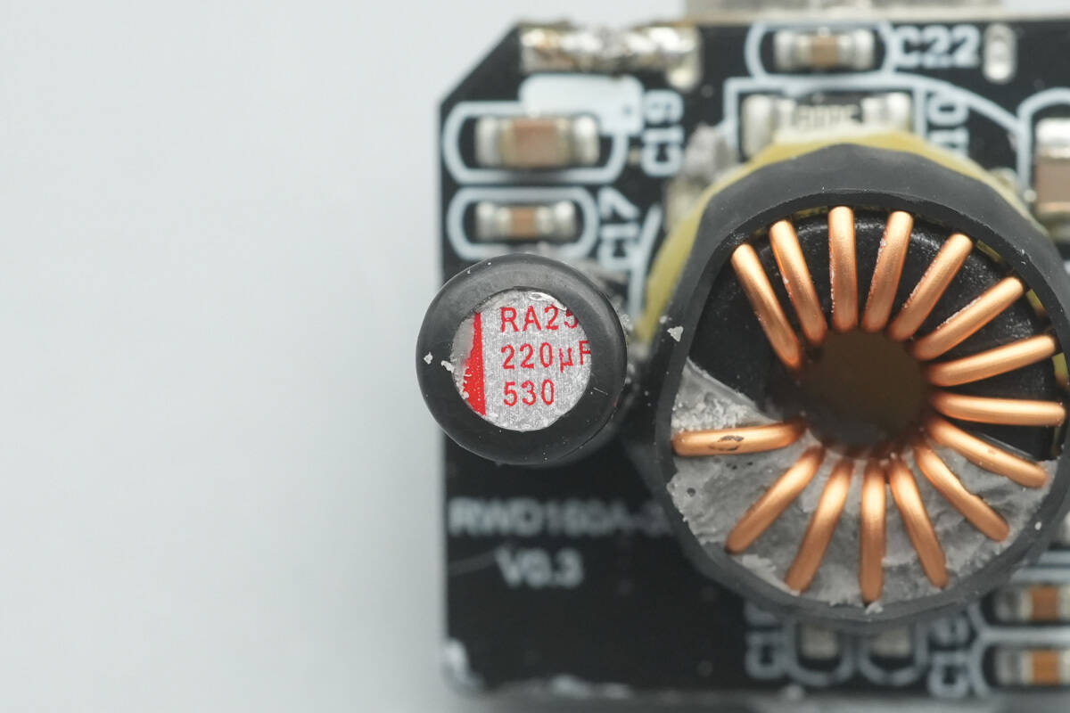
The secondary filter solid capacitor is rated at 25 V 220 μF.
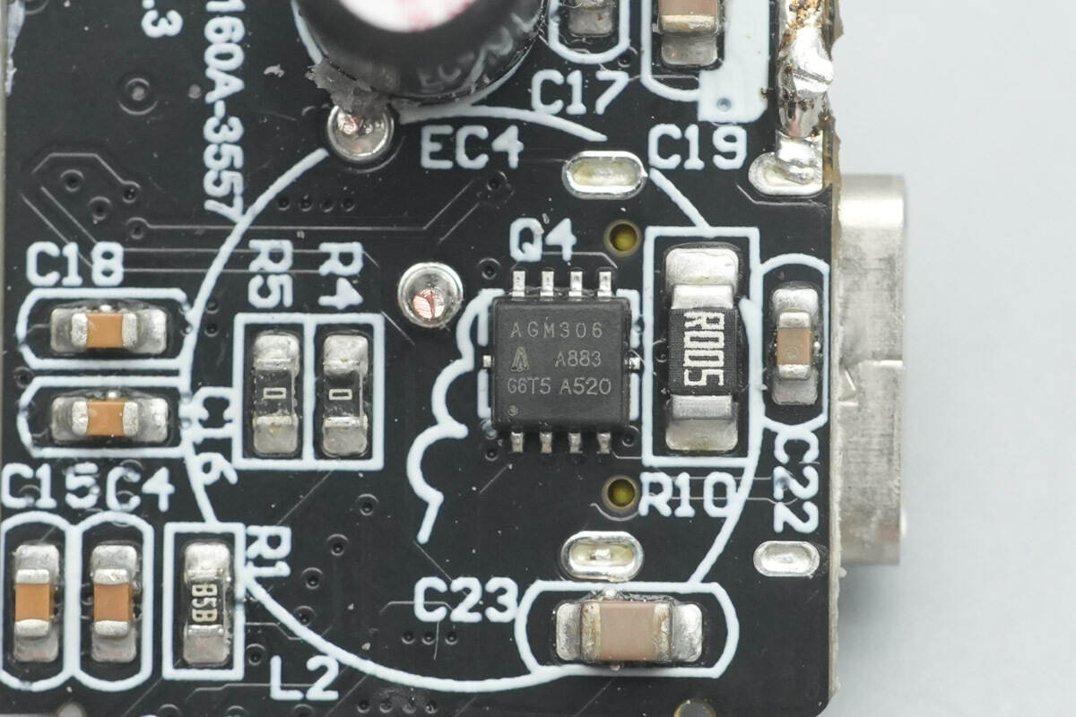
The output VBUS MOSFET located beneath the inductor is an AGM-Semi AGM306, an NMOS rated at 30 V with an on-resistance of 5.7 mΩ, packaged in DFN 3.3×3.3.

The other output VBUS MOSFET is also an AGM-Semi AGM306.

Close-up of the USB-C1 socket.
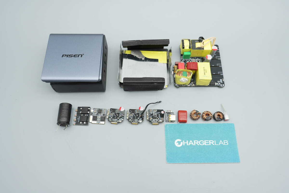
Well, those are all components of the Pisen 160W 4-USB-C GaN Charger.
Summary of ChargerLAB
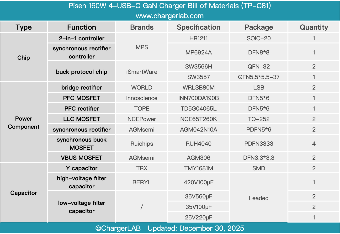
Here is the component list of the Pisen 160W 4-USB-C GaN Charger for your convenience.
It features four USB-C ports, compatible with multiple fast-charging protocols including QC, PD, and PPS. The total maximum output power for simultaneous multi-port charging is 160 W, significantly improving charging efficiency. It also comes with a 240 W braided cable.
After taking it apart, we found that it is based on a highly integrated and efficient PFC + LLC power design using the MPS HR1211 and MP6924A, paired with Innoscience INN700DA190B GaN power device. The output features three independent DC-DC buck circuits using the iSmartWare SW3566H and SW3557 solutions. The module is covered with heatsinks and insulated, and a thermistor is installed for temperature monitoring.
Related Articles:
1. Teardown of Highsay C1 Pro 140W Ultra Charger
2. Teardown of Belkin BoostCharge Pro 140W Braided USB-C to Dual USB-C Cable (CAC004)
3. Teardown of Baseus T-Space 3rd Generation 60W GaN Charger Dock for Tesla (BS-TS017)