Introduction
Huawei has recently launched its first 100W flagship all-in-one power bank, featuring a brand-new built-in USB-C cable. The cable uses liquid silicone material and integrates a magnetic storage slot, allowing users to pull it out to charge and snap it back into place effortlessly. This design combines excellent portability with a smooth, premium feel. The power bank also introduces HarmonyOS Smart Display, enabling users to check the remaining battery level and charging status directly on their Huawei smartphones in real time.
In terms of performance, it comes with an additional USB-C port. Both the built-in cable and the port support 100 W PD/UFCS as well as 66 W SCP fast charging, delivering powerful and versatile charging capabilities. With pass-through charging and smart dynamic power distribution, the power bank can efficiently charge two devices simultaneously.
For safety, it houses high-quality ATL flagship smartphone battery cells with ceramic separator insulation, and has passed China’s 3C, EU CE, and international CB certifications. It also debuts a four-way NTC temperature monitoring system, which intelligently regulates temperature in real time to prevent overheating during charging. Let’s take a closer look inside this impressive power bank.
Product Appearance
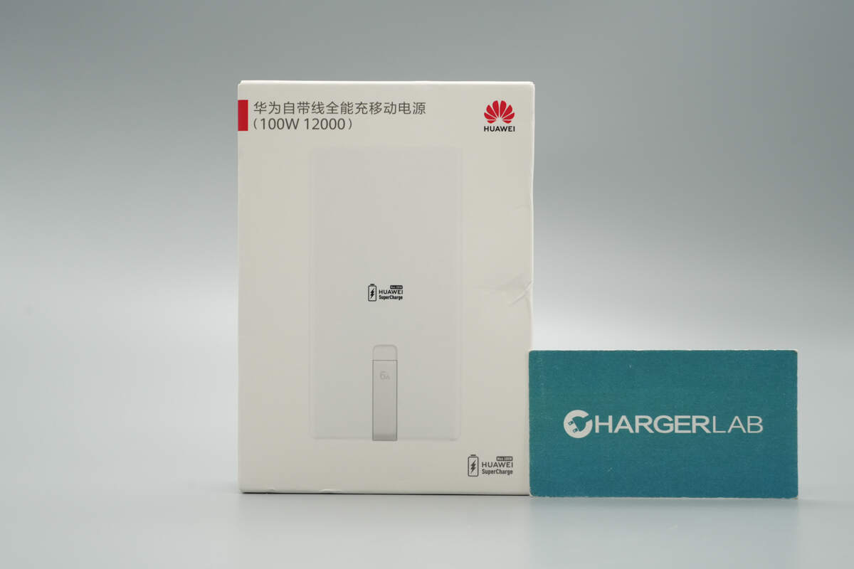
The front of the packaging features the Huawei logo, the product name, and an image of the power bank.

The back of the packaging displays key selling points, certification information, and other product details.
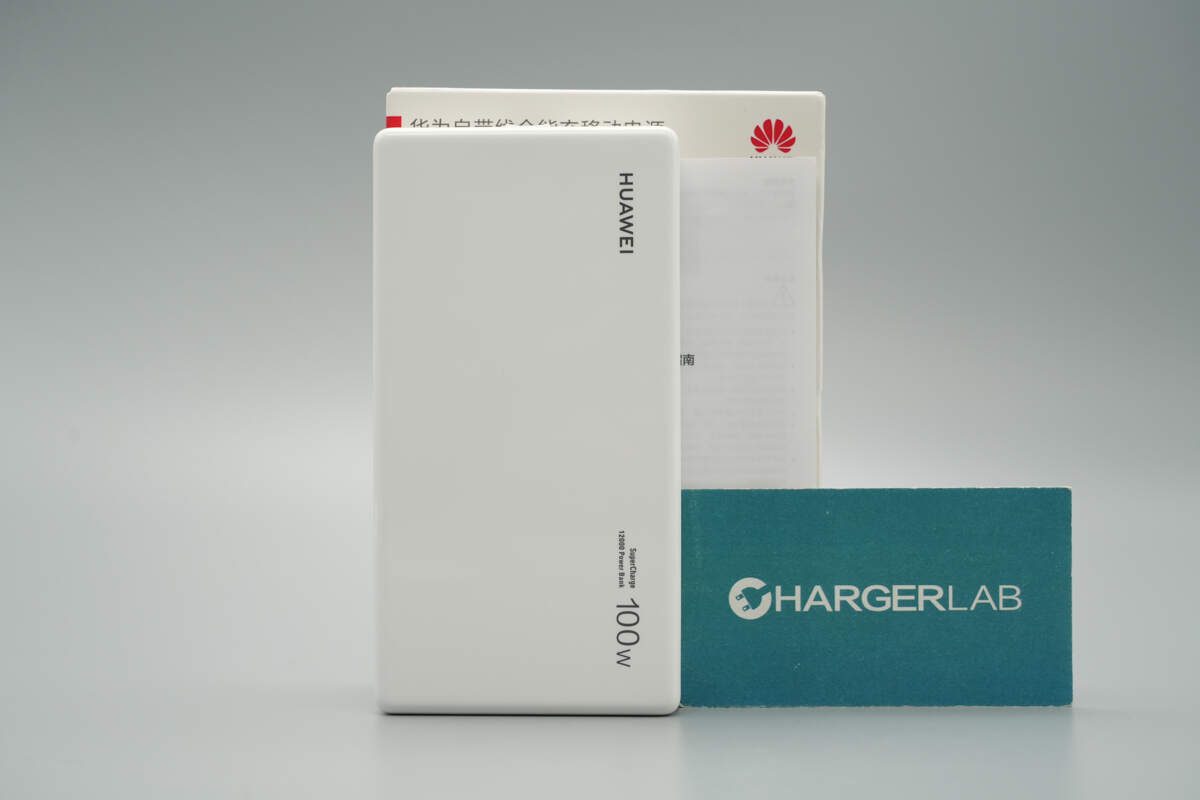
Inside the box, you'll find the power bank and a user guide.

It comes in two color options: black and white. The smooth, rounded edges and slim profile make it comfortable to hold.
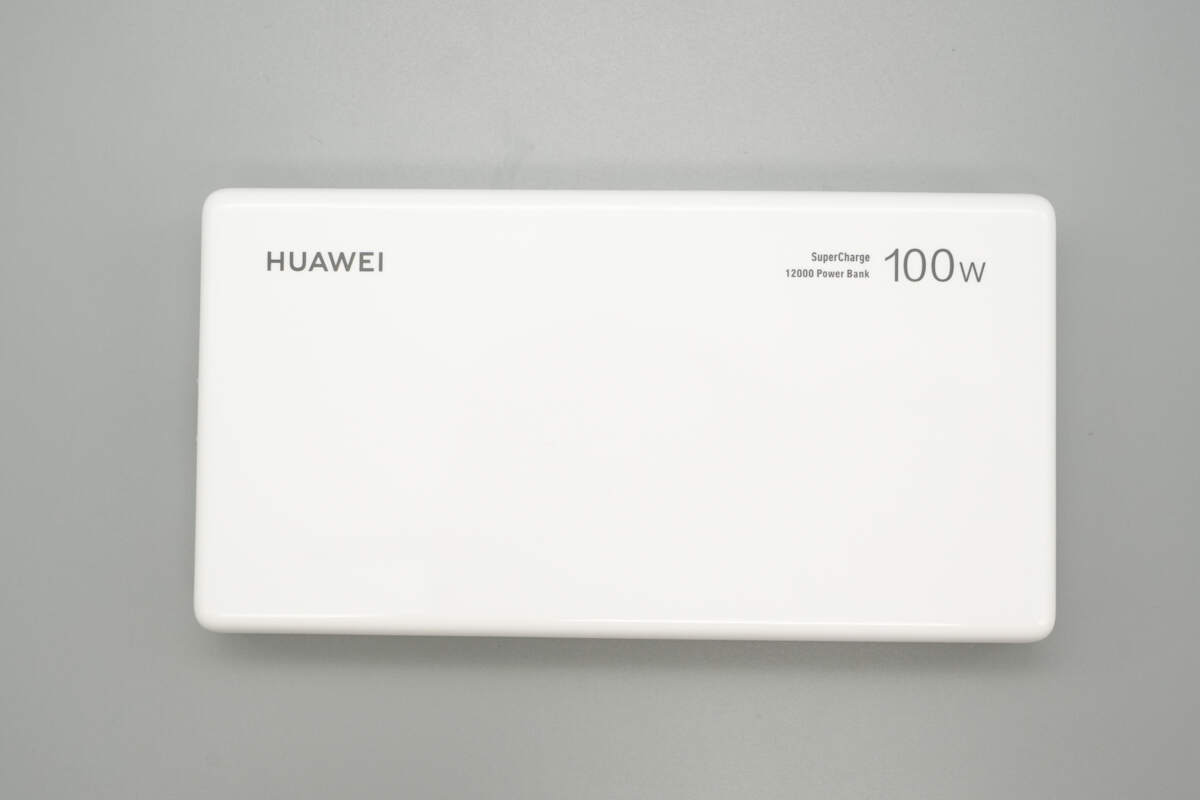
The front is printed with the HUAWEI logo and “100W” markings.
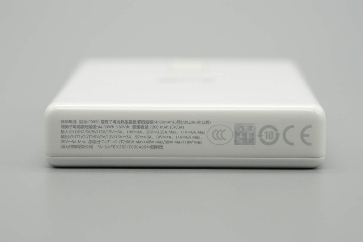
The specifications are printed on the end of the power bank.

Model: P0020
Typical/Rated Li-ion Battery Capacity: 4020 mAh (3 cells) / 3920 mAh (3 cells)
Rated Li-ion Battery Energy: 44.93 Wh, 3.82 V DC
Rated Capacity: 7200 mAh (5 V 3 A)
Input:
IN1/IN2: 5/9/12/15 V ⎓ 3 A, 10 V ⎓ 4 A, 20 V ⎓ 3.25 A Max, 11 V ⎓ 6 A Max
Output:
OUT1/OUT2: 5/9/12/15 V ⎓ 3 A, 5 V ⎓ 4.5 A, 10 V ⎓ 4 A, 11 V ⎓ 6 A Max, 20 V ⎓ 5 A Max
Total Output (OUT1 + OUT2): 66 W Max + 40 W Max / 88 W Max + 18 W Max
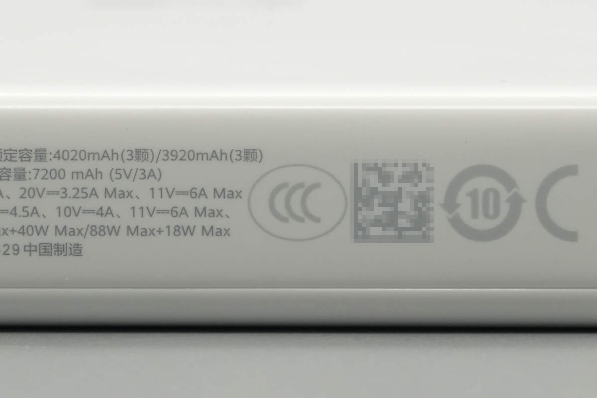
It has passed CCC and CE certifications.
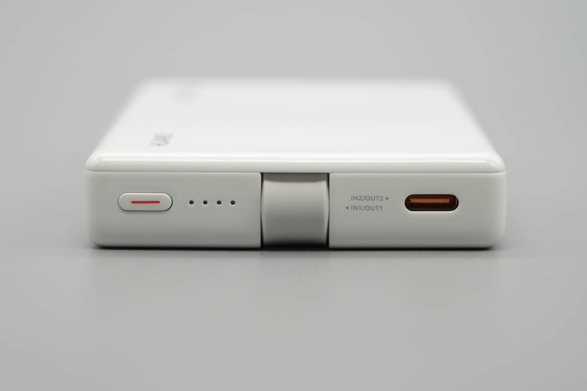
The other end features a power button, battery indicator lights, a built-in USB-C cable, and a USB-C2 port.

The battery indicator lights glow white, with each light representing 25% of the charge.
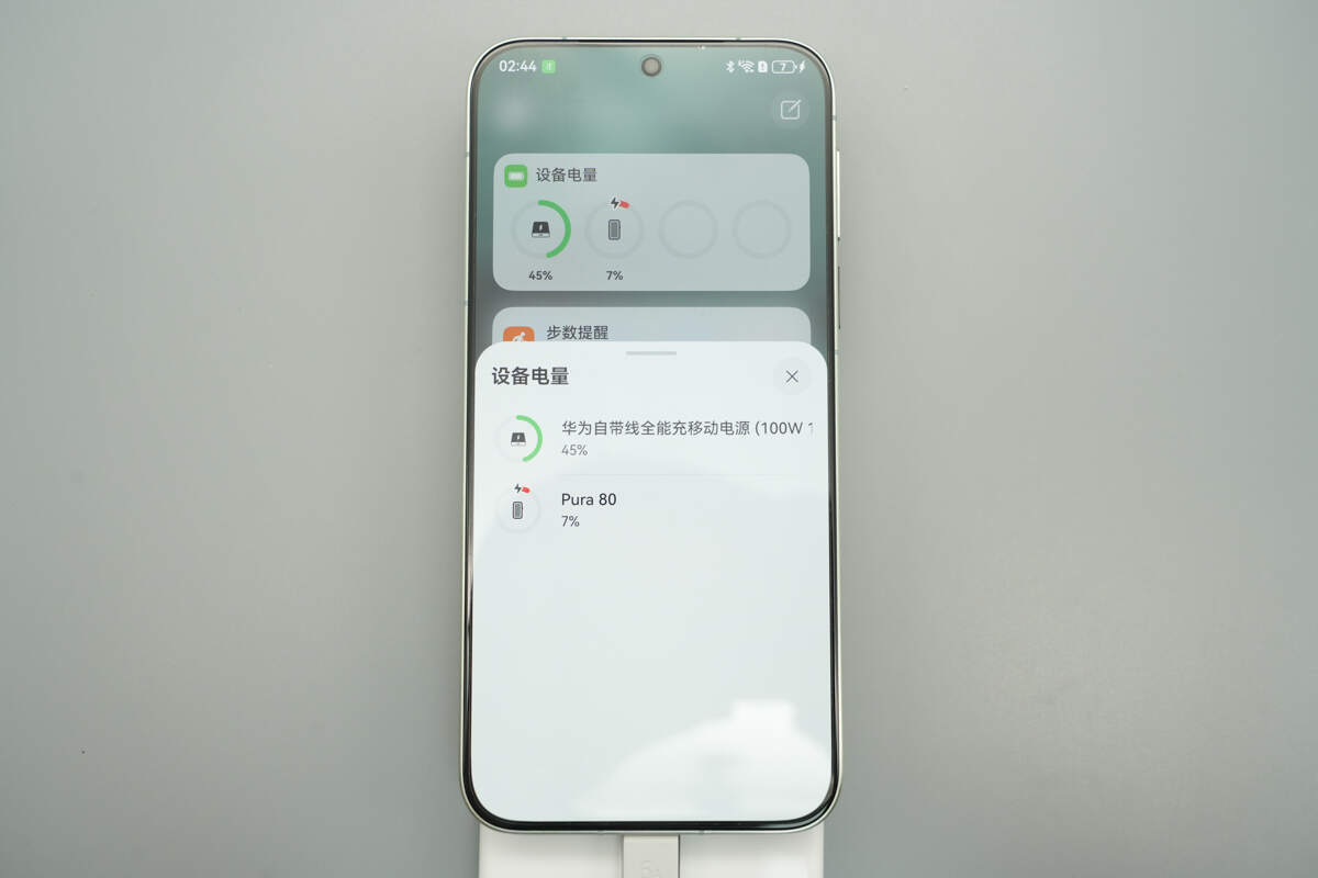
It supports HarmonyOS Smart Display, allowing users to check the remaining power of the power bank on their smartphones while charging.
The built-in USB-C cable has a flat design, and the outer layer is made of liquid silicone material.
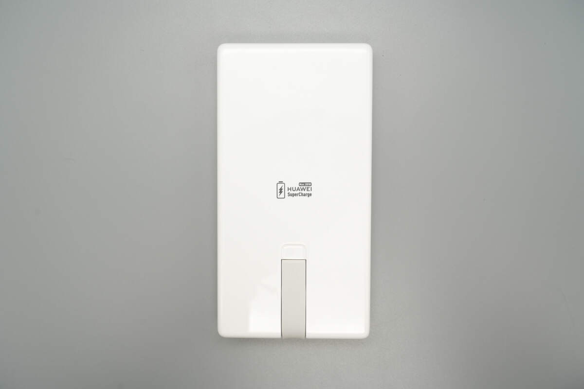
The back features a storage slot for the built-in USB-C cable.
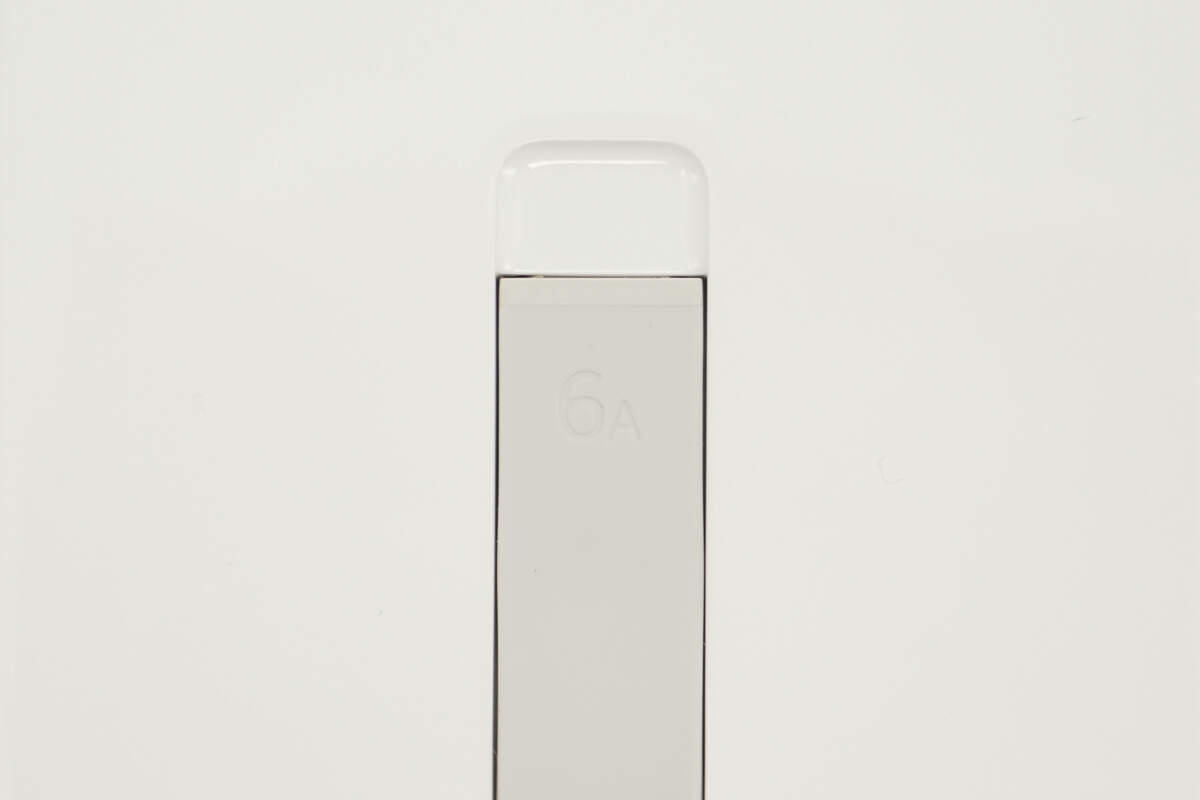
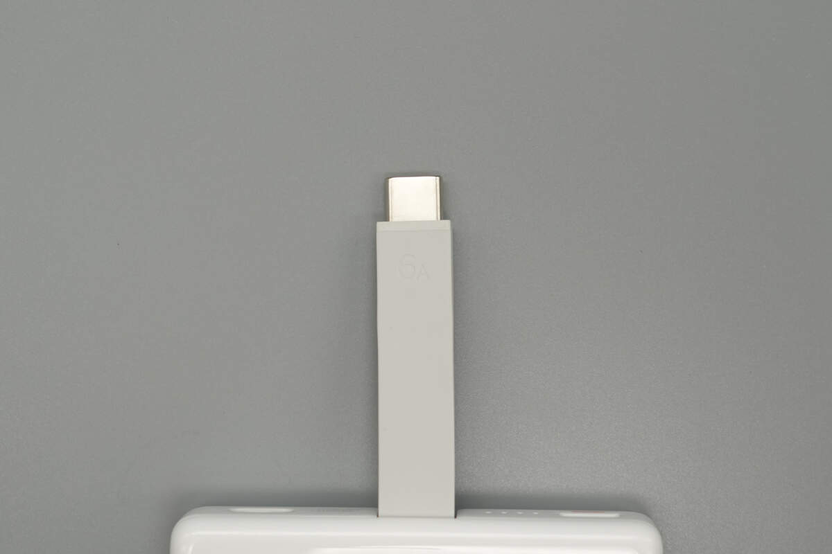
The built-in cable is marked with 6A.
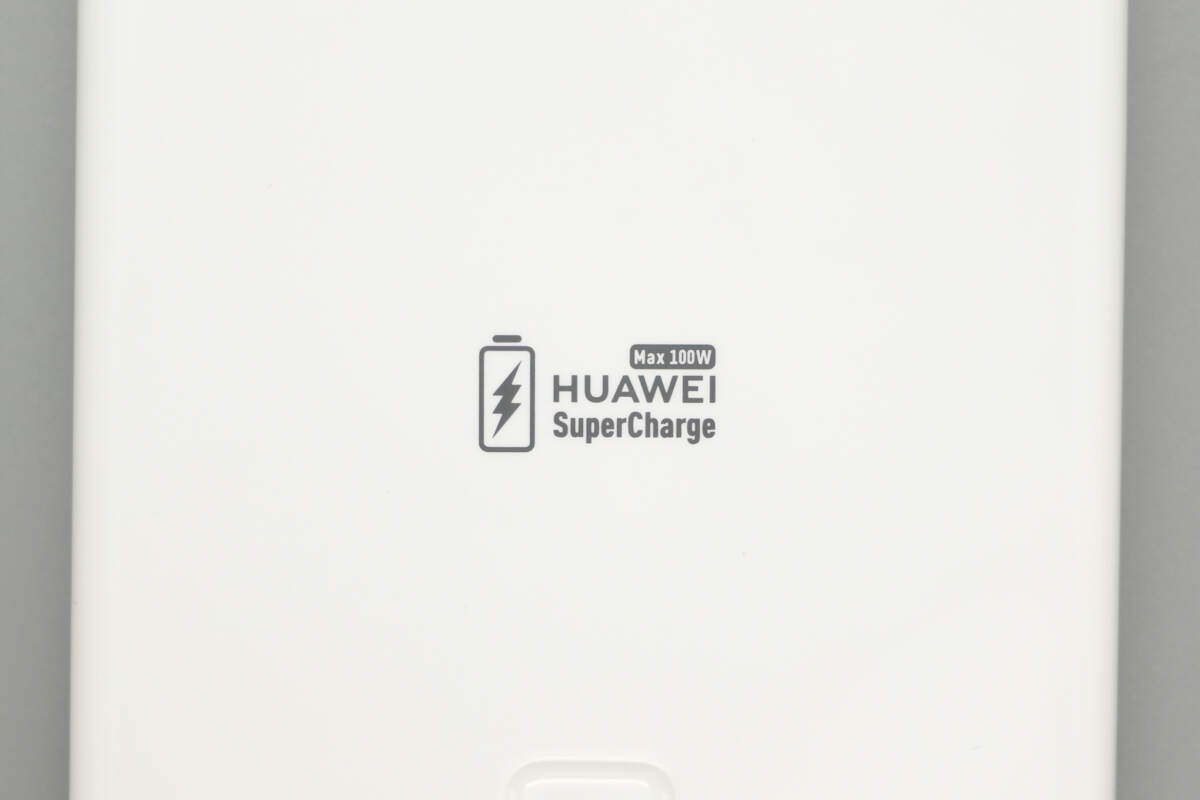
The center is printed with Max 100W and HUAWEI SuperCharge.
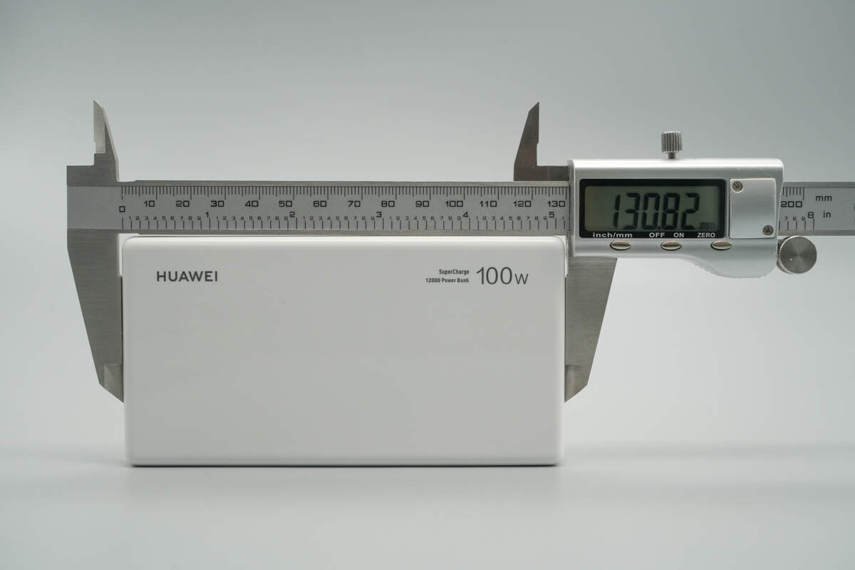
The length of the power bank is about 130.82 mm (5.15 inches).
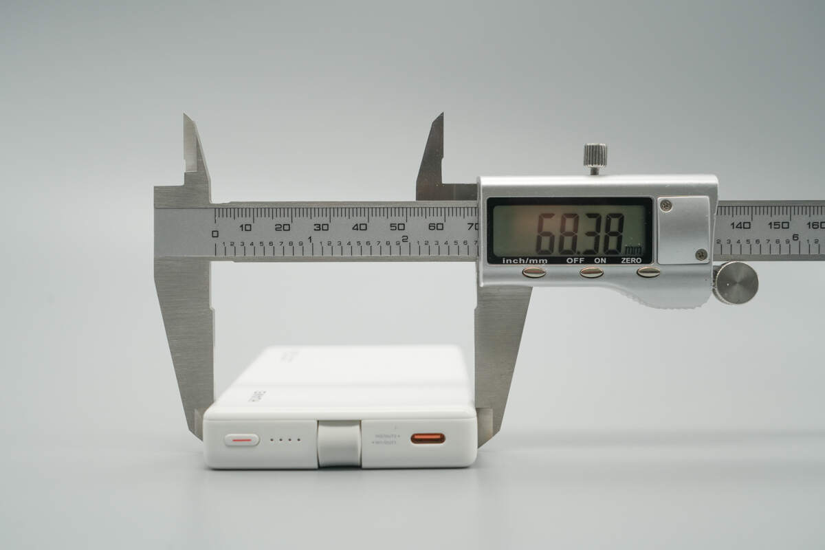
The width is about 68.38 mm (2.69 inches).

The thickness is about 15.72 mm (0.62 inches).
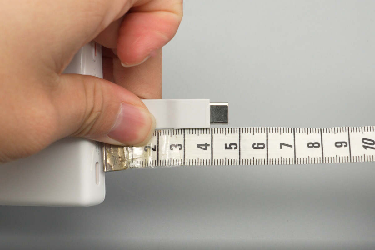
The length of the built-in USB-C cable is about 4.5 cm (1.77 inches).
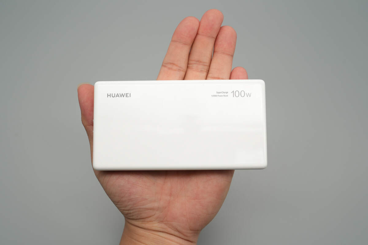
That's how big it is in the hand.

The weight is about 238 g (8.4 oz).

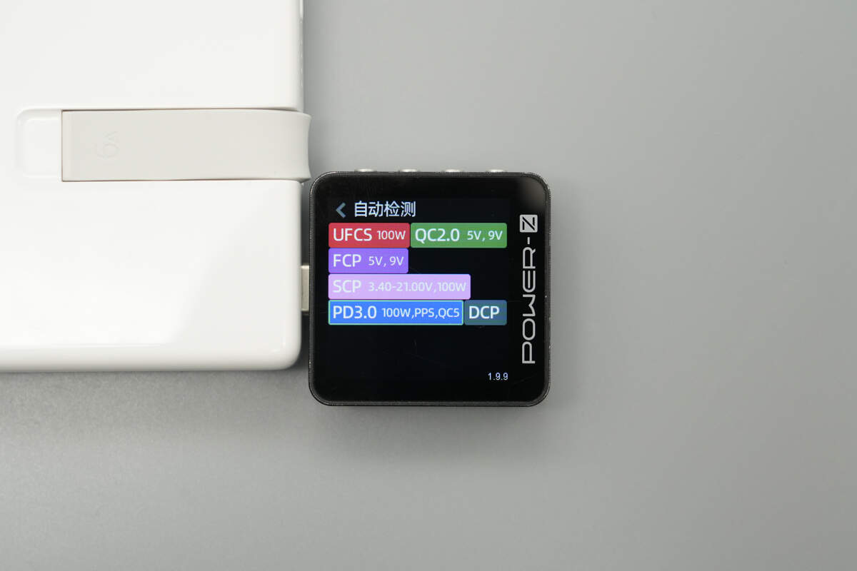
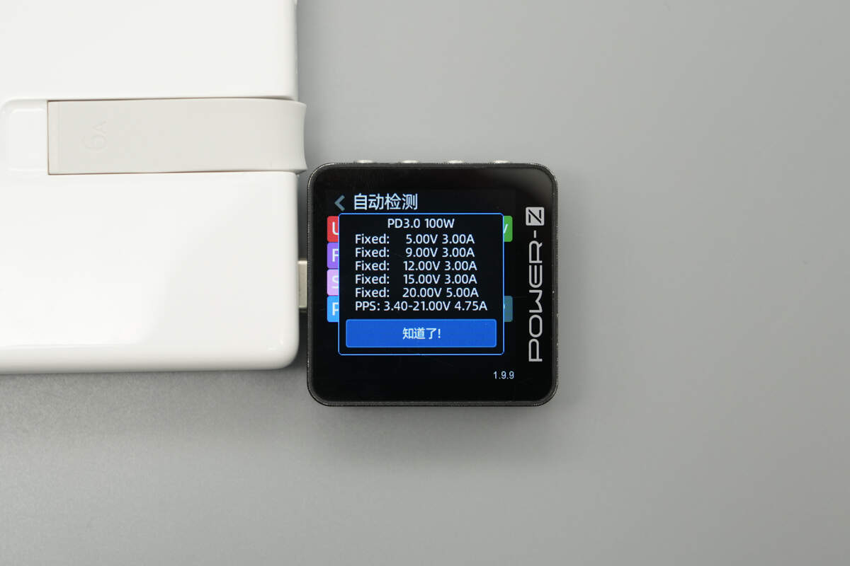
ChargerLAB POWER-Z KM003C shows that the build-in USB-C cable supports UFCS, QC2.0/5, FCP, SCP, PD3.0, PPS, and DCP charging protocols.
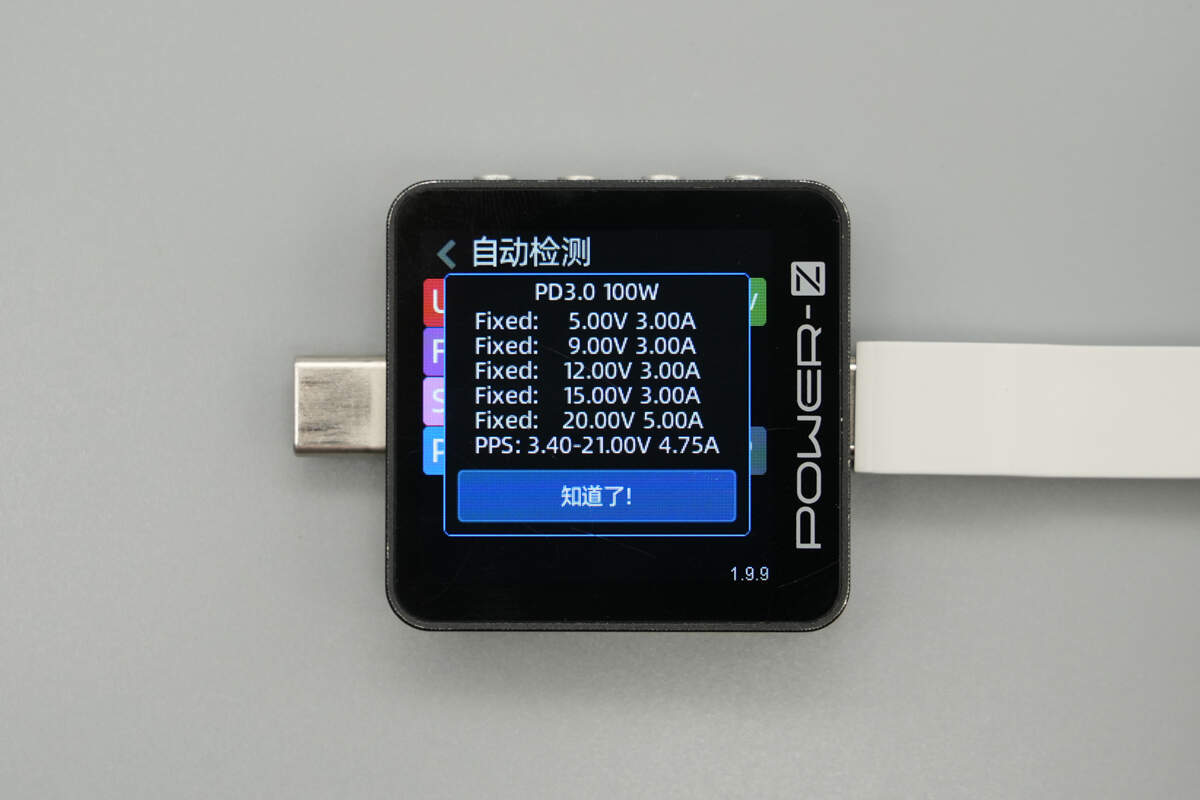
And it has five fixed PDOs of 5V3A, 9V3A, 12V3A, 15V3A, and 20V5A. It has one set of PPS, which is 3.4-21V4.75A.
The USB-C2 port supports the same charging protocols as the built-in USB-C cable.
The PDO reports are also identical.
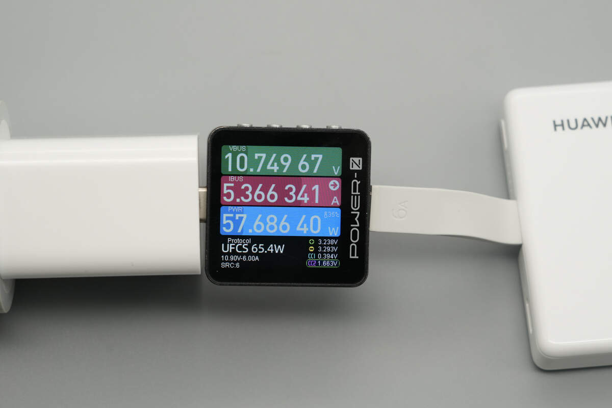
When charging the power bank using a Huawei 100W charger via the built-in USB-C cable, the measured output power of the charger is about 57.69W.

When charging the Huawei Mate 70 Pro+ using the power bank’s built-in USB-C cable, the measured charging power is about 70.03W.
Teardown
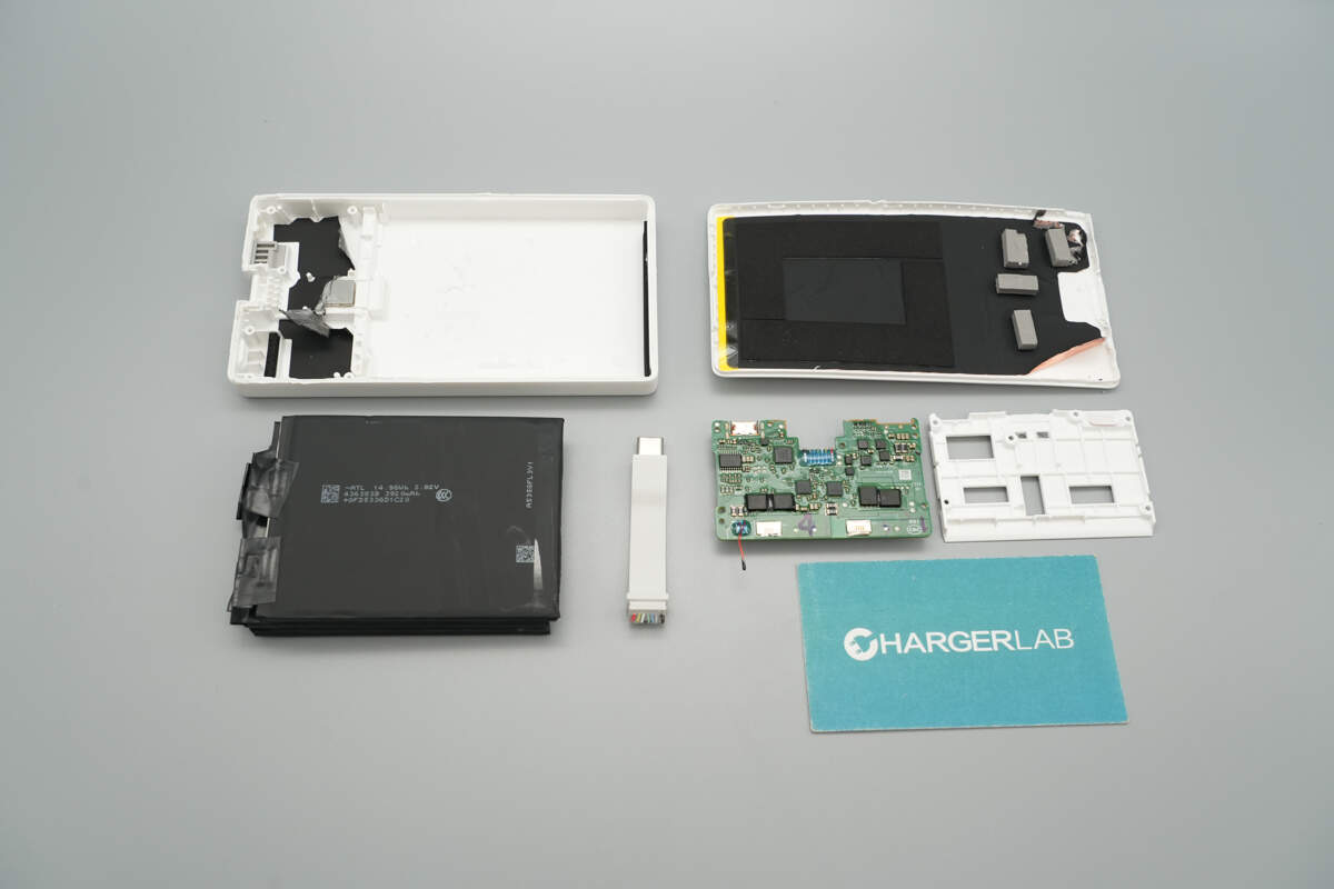
Next, let's take it apart to see its internal components and structure.
Remove the front casing. The PCB is covered with a white plastic plate for insulation. Areas corresponding to the main heat-generating components are cut out and fitted with thermal pads to facilitate heat dissipation.
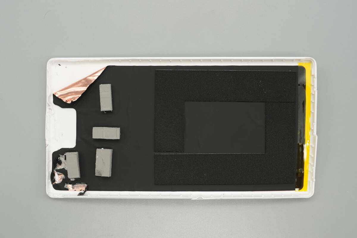
The inner side of the casing is lined with copper foil, thermal pads, and foam.

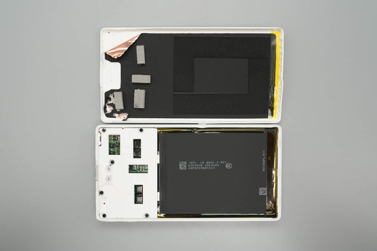
Remove the white plastic plate. The battery cells are connected to the PCB via nickel strips spot welding.
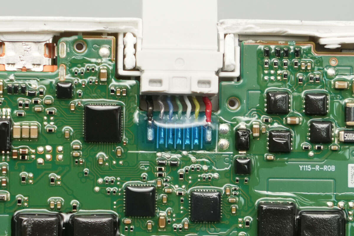
The connection between the built-in USB-C cable and the PCB is secured with adhesive for protection.
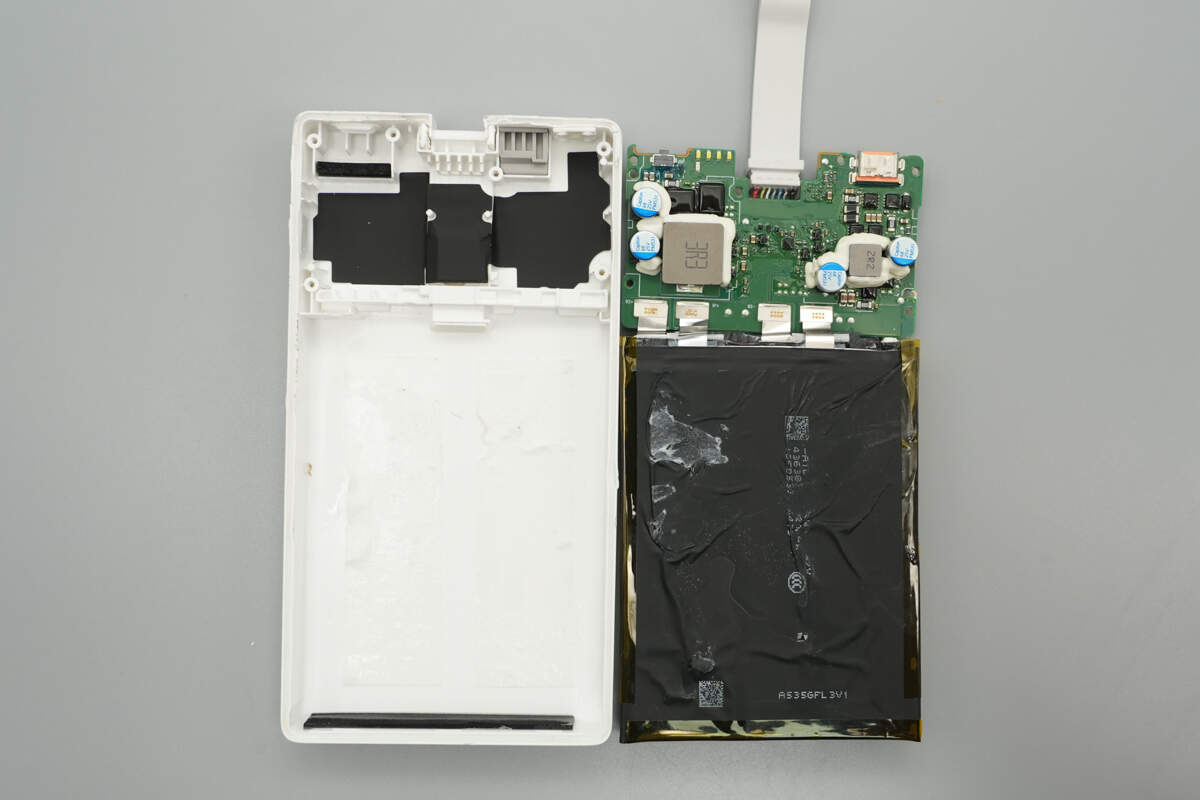
Remove the PCB and battery cells.
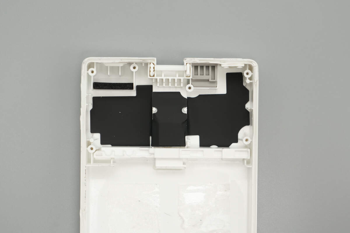
The other half of the casing, corresponding to the PCB area, is lined with graphite thermal tape.
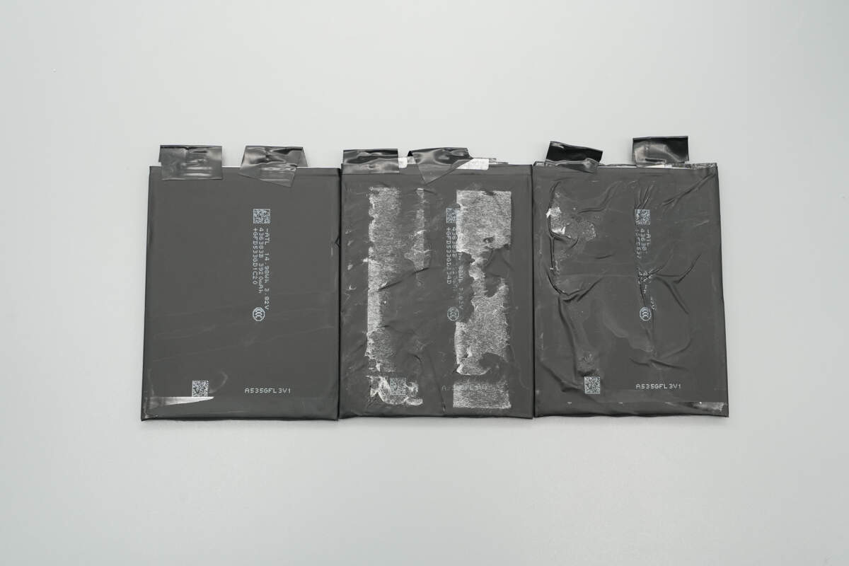
The battery pack consists of three cells.

All three battery cells share the same part number and are from ATL, model 436383B, with a nominal voltage of 3.82 V and a nominal capacity of 3920 mAh. They have passed CCC and CE certifications and comply with UL1642 and IEC62133 safety standards.
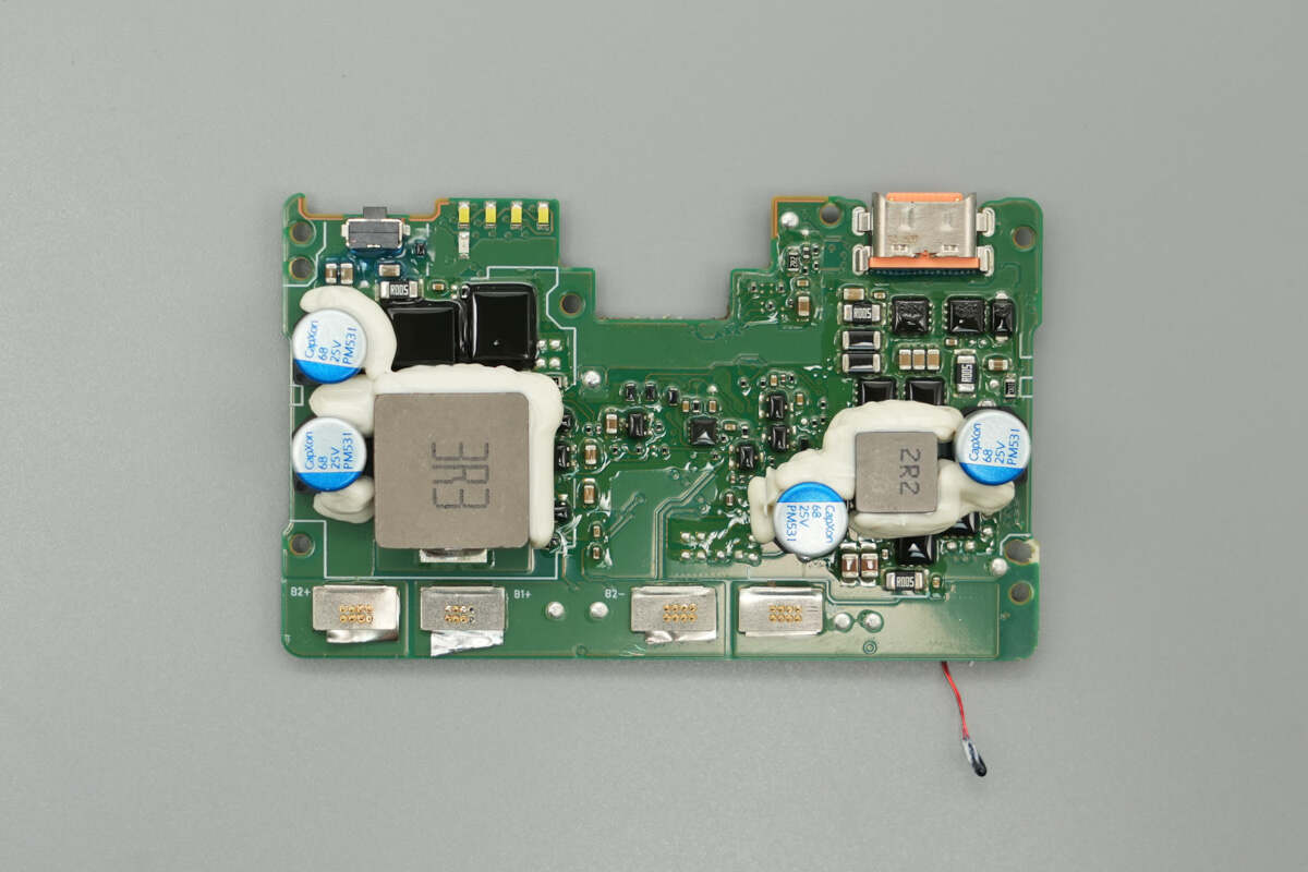
The front side of the PCB features synchronous buck-boost MOSFETs, VBUS MOSFETs, an E-Marker chip, inductors, and solid capacitors.
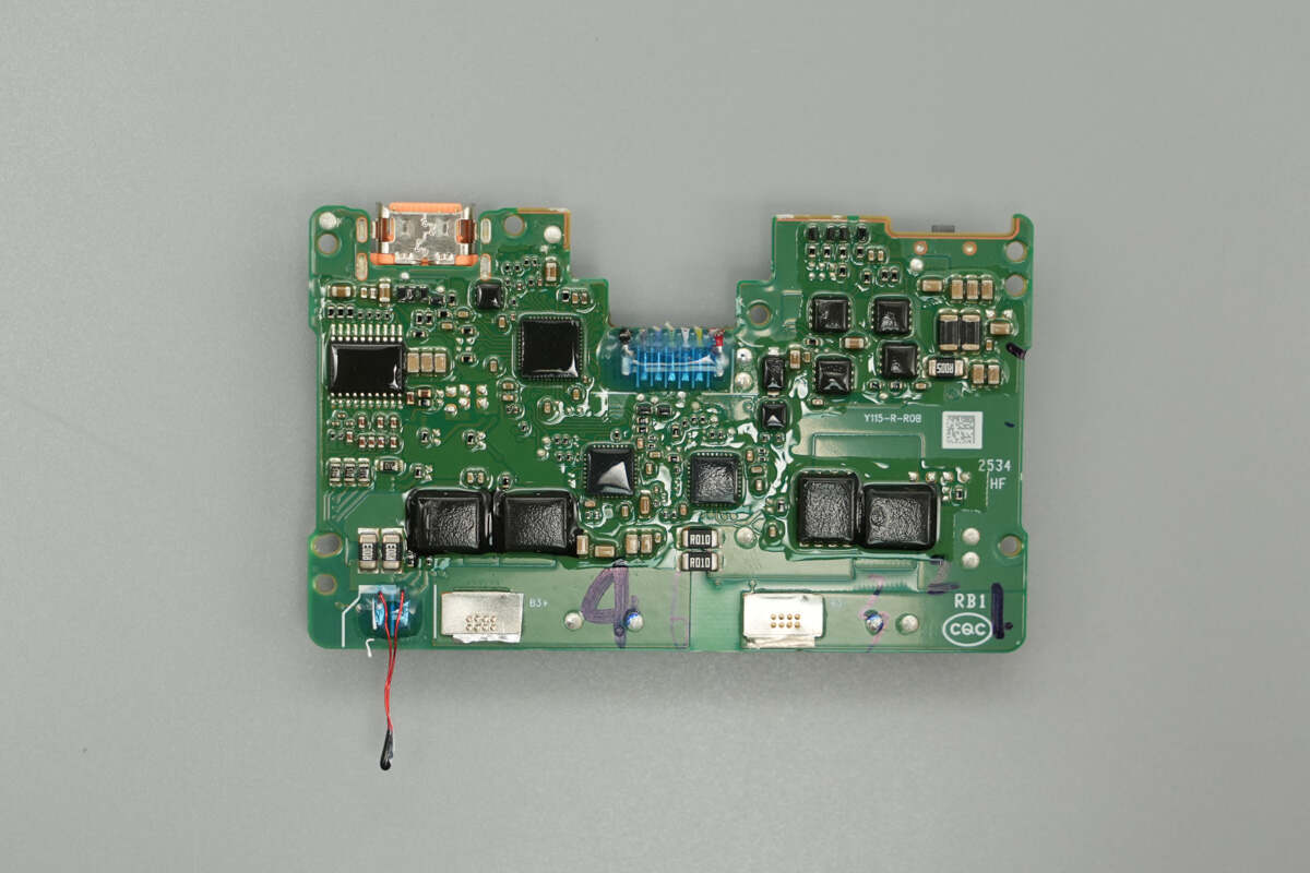
The back side of the PCB is equipped with a battery protection chip, battery protection MOSFETs, a synchronous buck-boost controller, synchronous buck-boost MOSFETs, a protocol chip, VBUS MOSFETs, and a thermistor.
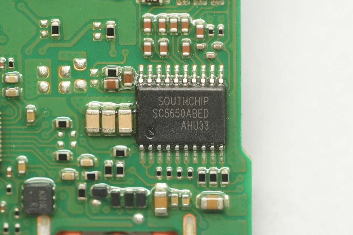
The battery protection chip is from SouthChip, model SC5650. It is designed for 2–5 series battery packs and provides protections including overvoltage, undervoltage, three-level overcurrent during discharge, and overcurrent during charging. It also supports an external NTC thermistor for high/low temperature battery protection and chip overheat shutdown.
The SC5650 supports cascaded applications, allowing two chips to be used for 6–10 series battery packs. It features extremely low quiescent current and high protection accuracy, with multiple variants available to accommodate different voltages and battery types.
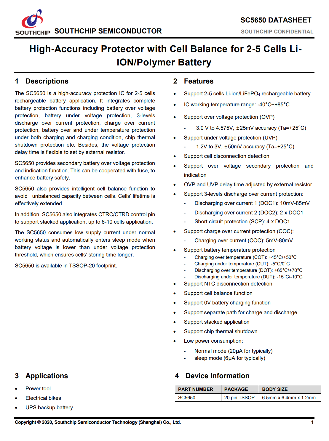
Here is the information about SouthChip SC5650.
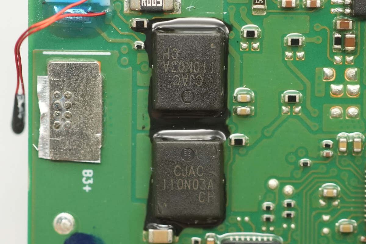
The battery protection MOSFETs are from JSCJ, model CJAC110N03A. They are N-channel MOSFETs with a voltage rating of 30 V and an on-resistance of 1.8 mΩ, packaged in a PDFNK 6 5×6-8L package.

The synchronous buck-boost controllers for both the built-in USB-C cable and the USB-C2 port are SouthChip SC8815A. This is a high-efficiency, bidirectional synchronous buck-boost controller that supports charging 1–6 series battery cells and features an I²C interface. It provides full lithium battery charging management, allowing battery charging current and voltage, reverse discharge output voltage, and input/output current limits to be controlled via the I²C bus.
The SC8815A integrates a 10-bit ADC and provides charging status indication. It supports automatic adapter and load insertion detection, undervoltage protection, overvoltage protection, overcurrent protection, short-circuit protection, and overheat shutdown. The chip comes in a QFN32 package and is suitable for PD fast-charging power banks, USB-C hubs, and industrial power applications.
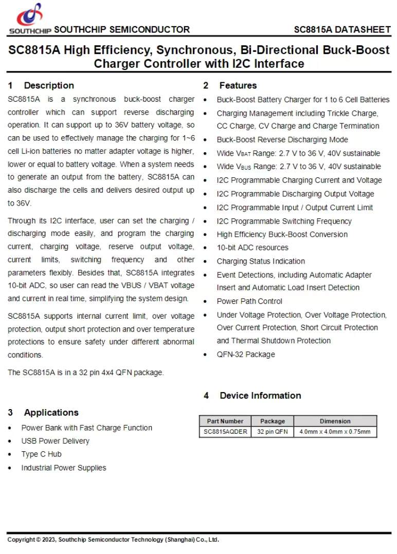
Here is the information about SouthChip SC8815A.

The synchronous buck-boost MOSFETs for the built-in USB-C cable’s buck-boost circuit are from Vergiga, model VS3610GPMT. They are N-channel MOSFETs with a voltage rating of 30 V and an on-resistance of 2.5 mΩ, packaged in a PDFN 5×6 package.
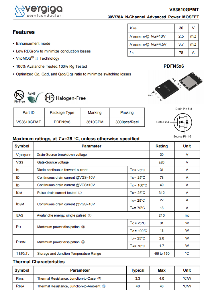
Here is the information about Vergiga VS3610GPMT.
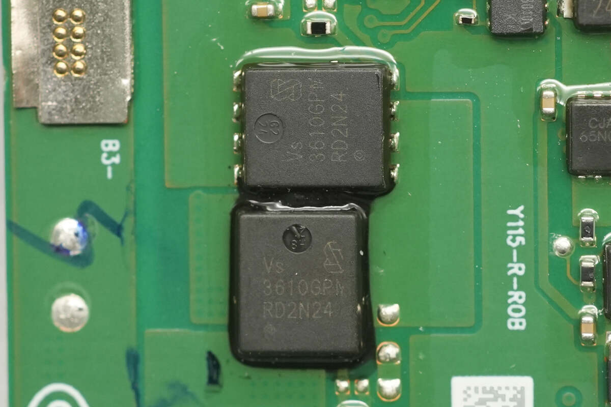
The other two Vergiga VS3610GPMT synchronous buck-boost MOSFETs are located on the back side of the PCB.

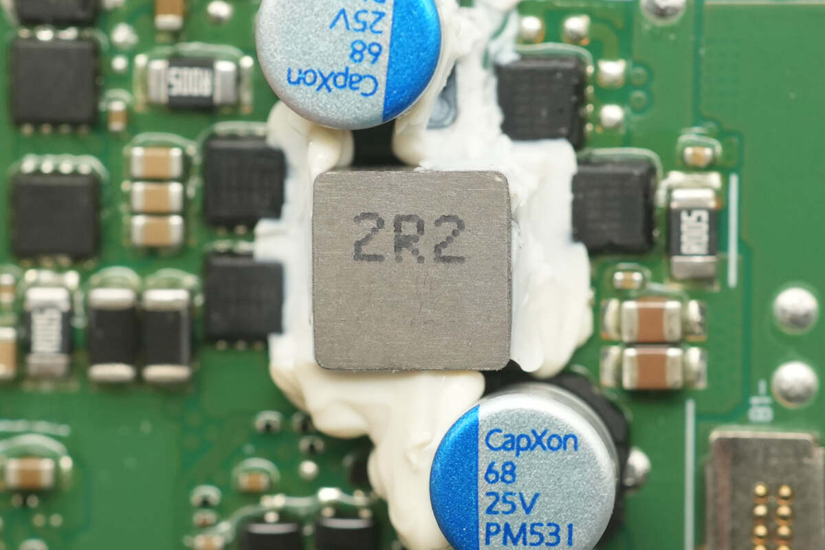
Close-up of the 3.3 μH buck-boost inductor.

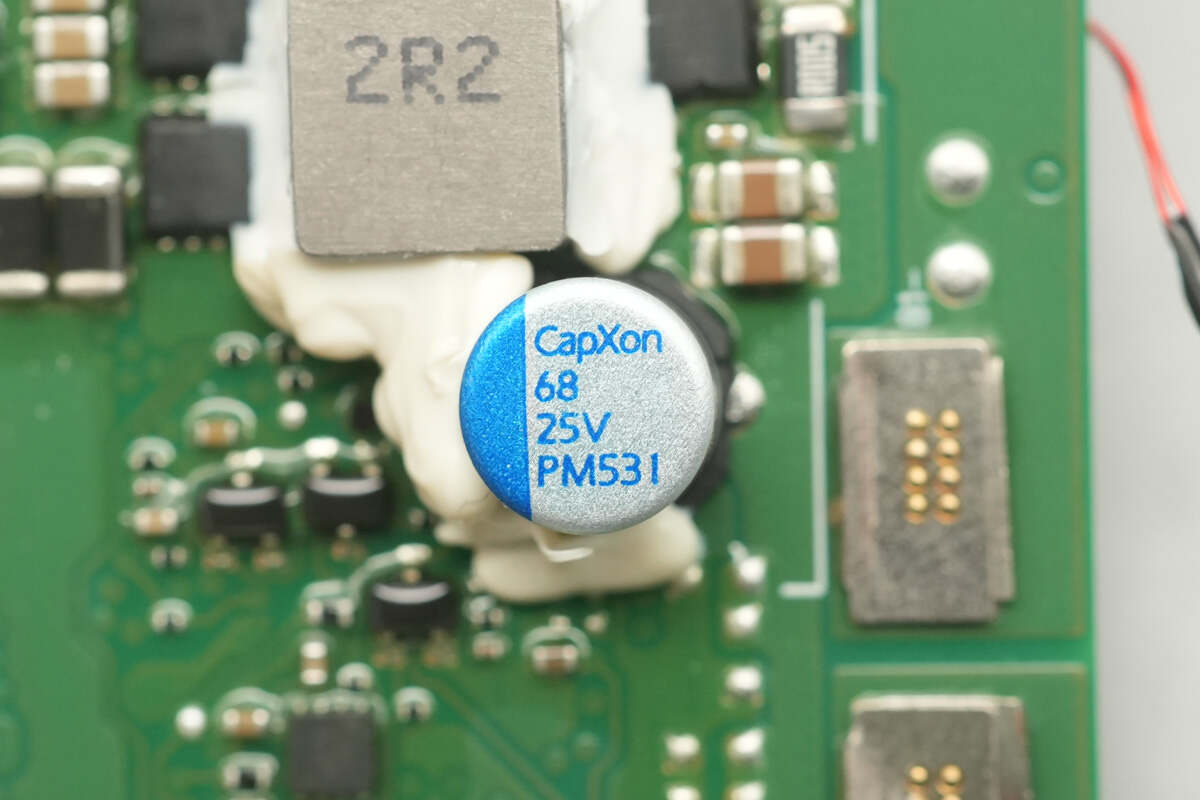
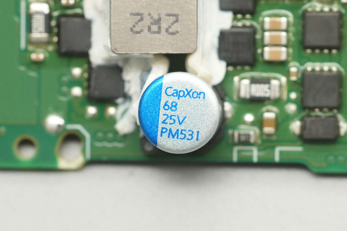
The two solid capacitors are from CapXon, each rated at 25 V and 68 μF.

The synchronous buck-boost MOSFETs for the USB-C2 port’s buck-boost circuit are Vergiga VS3610AE, N-channel MOSFETs with a voltage rating of 30 V and an on-resistance of 4 mΩ, packaged in PDFN3333.

Here is the information about Vergiga VS3610AE.

The other two Vergiga VS3610AE synchronous buck-boost MOSFETs are positioned on the other side of the inductor.
Close-up of the 2.2 μH buck-boost inductor.
The solid capacitor is also from CapXon, rated at 25 V and 68 μF.
The other solid capacitor has the same part number.
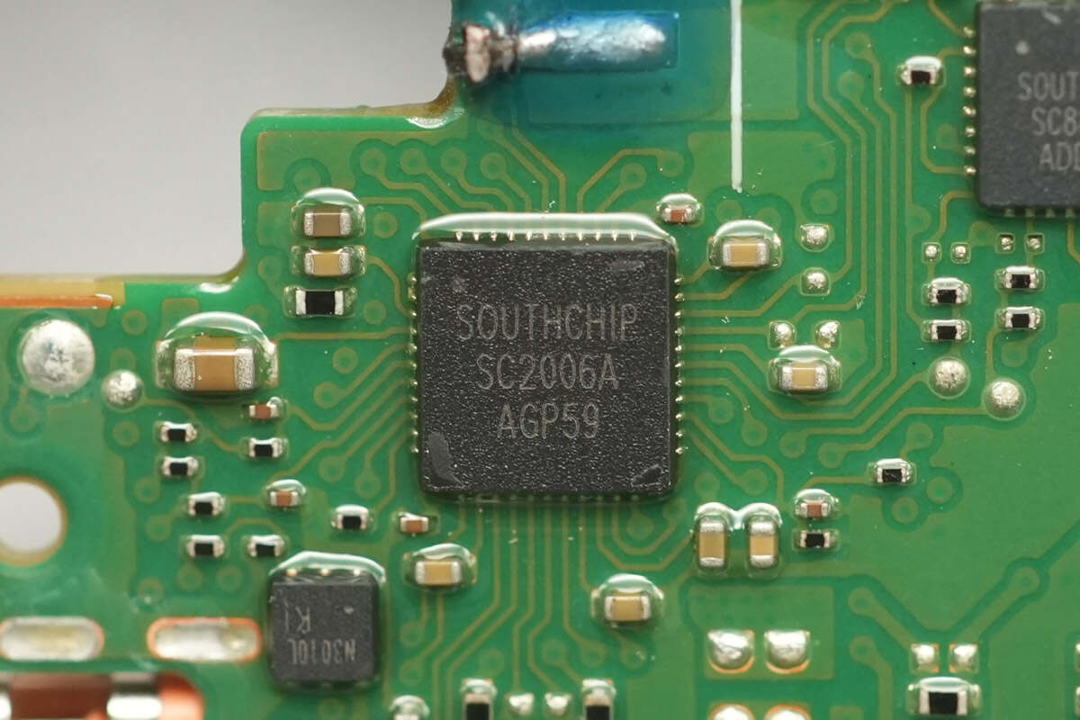
The protocol chip for both the built-in USB-C cable and the USB-C2 port is SouthChip SC2006A, a fast-charging controller that supports three Type-C DRP ports. It is compatible with all major fast-charging protocols and features CC and DPDM interfaces. Its target applications include power banks, car chargers, and power tools.
The SC2006A integrates Type-C/PD circuits, DPDM/UFCS fast-charging circuits, VBUS discharge paths, voltage and current detection, an 11-bit high-performance ADC, two 11-bit DACs, NMOS gate drivers, an I²C interface, and protection circuits, minimizing the need for external components.

The SC2006A features a built-in 32-bit high-performance microcontroller with 128 KB of flash memory and 8 KB of SRAM, offering a cost-effective solution for various applications. It also supports multiple protection mechanisms, including overvoltage, undervoltage, overcurrent, short-circuit, over-temperature, DPDM overvoltage, CC overvoltage, and VCONN overvoltage/overcurrent/short-circuit protections, ensuring stable and reliable system operation.

The MOSFET marked with N3010L is from JSCJ, model CJMN3010L. It is an N-channel MOSFET with a voltage rating of 30 V and an on-resistance of 8.3 mΩ, packaged in a DFNWB 2×2-6L package.
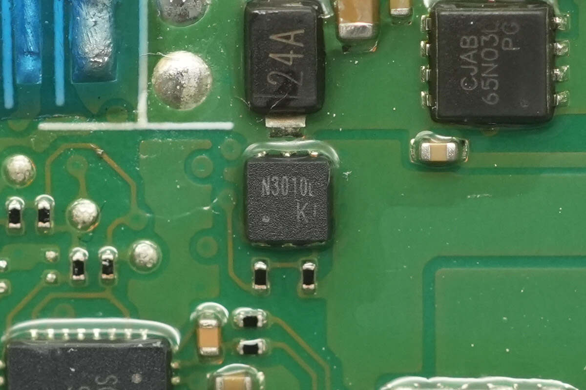
Close-up of the other JSCJ CJMN3010L MOSFET.

The VBUS MOSFETs for the built-in USB-C cable are from JSCJ, model CJAB65N03L. They are N-channel MOSFETs with a voltage rating of 30 V and an on-resistance of 2.5 mΩ, packaged in PDFNWB 3.3×3.3-8L.
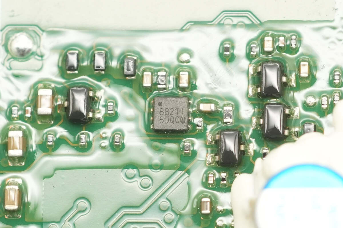
The E-Marker chip, marked with 8821H, is packaged in a DFN-8.

The VBUS MOSFETs for the USB-C2 port are also JSCJ CJAB65N03L.
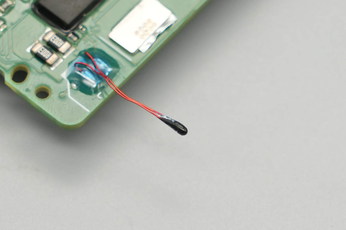
Close-up of the thermistor.
Well, those are all components of the Huawei SuperPower 100W 12000mAh Power Bank.
Summary of ChargerLAB

Here is the component list of the Huawei SuperPower 100W 12000mAh Power Bank for your convenience.
It supports 66W proprietary bidirectional fast charging and 100W PD/UFCS high-power fast charging, meeting the fast-charging needs of both Huawei and third-party devices. The pass-through charging feature allows simultaneous charging of the power bank and a smartphone. Smart dynamic power distribution enables the built-in cable and port to deliver flexible output combinations, such as 66W + 40W or 88W + 18W. It also supports HarmonyOS Smart Display, allowing users to check the remaining battery level of the power bank directly on their phones.
After taking it apart, we found that it uses three ATL cells connected in series. The higher battery voltage allows lower currents on the PCB during high-power output, ensuring efficiency and keeping heat generation under control. The design incorporates a full solution with the SouthChip SC5650 battery protection chip, SC8815A synchronous buck-boost controllers, and SC2006A protocol chip to provide battery protection and bidirectional fast-charging functionality.
CapXon solid capacitors are used, and both the capacitors and inductors are reinforced with adhesive. The front and back of the PCB are coated with conformal coating to protect the chips. Graphite thermal tape and copper foil are applied to the casing to assist heat dissipation, indicating high-quality materials and workmanship.
Related Articles:
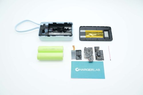
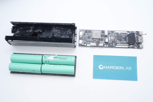
1. Teardown of EcoFlow RAPID Pro 230W 20,000mAh Power Bank with Built-in Cable (EF-HB-100)
2. Teardown of Nintendo Switch 2 Original 60W PD Fast Charger (Japan Version)
3. Teardown of Google 25W Qi2.2 Magnetic Wireless Charger (GH5UG)