Introduction
We recently got our hands on the EcoFlow RAPID Pro GaN Desktop Charger. This device delivers up to 320W of total output power and features a 3.02-inch display, with app-based customization and real-time monitoring via a connected app. The display supports clock mode, interactive idle animations, and dynamic charging effects.
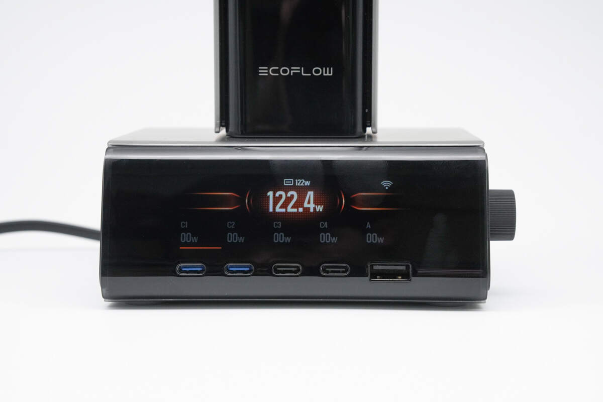
The front panel includes four USB-C ports and one USB-A port. Both USB-C1 and USB-C2 support up to 140W fast charging, capable of simultaneously charging two MacBooks at full speed. The USB-C3 port supports 65W fast charging, while USB-C4 and the USB-A port each support 30W fast charging.
On top, a POGO PIN magnetic connector provides an output power of 320W, designed to quickly and efficiently recharge the EcoFlow RAPID Pro series of power banks. Below, we take a closer look at the internal components and design.
Product Appearance
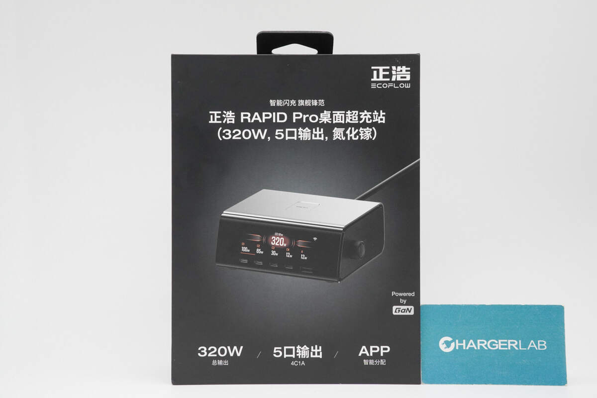
The front of the packaging box features the ECOFLOW logo, the product name, an image of the device, and key selling points.
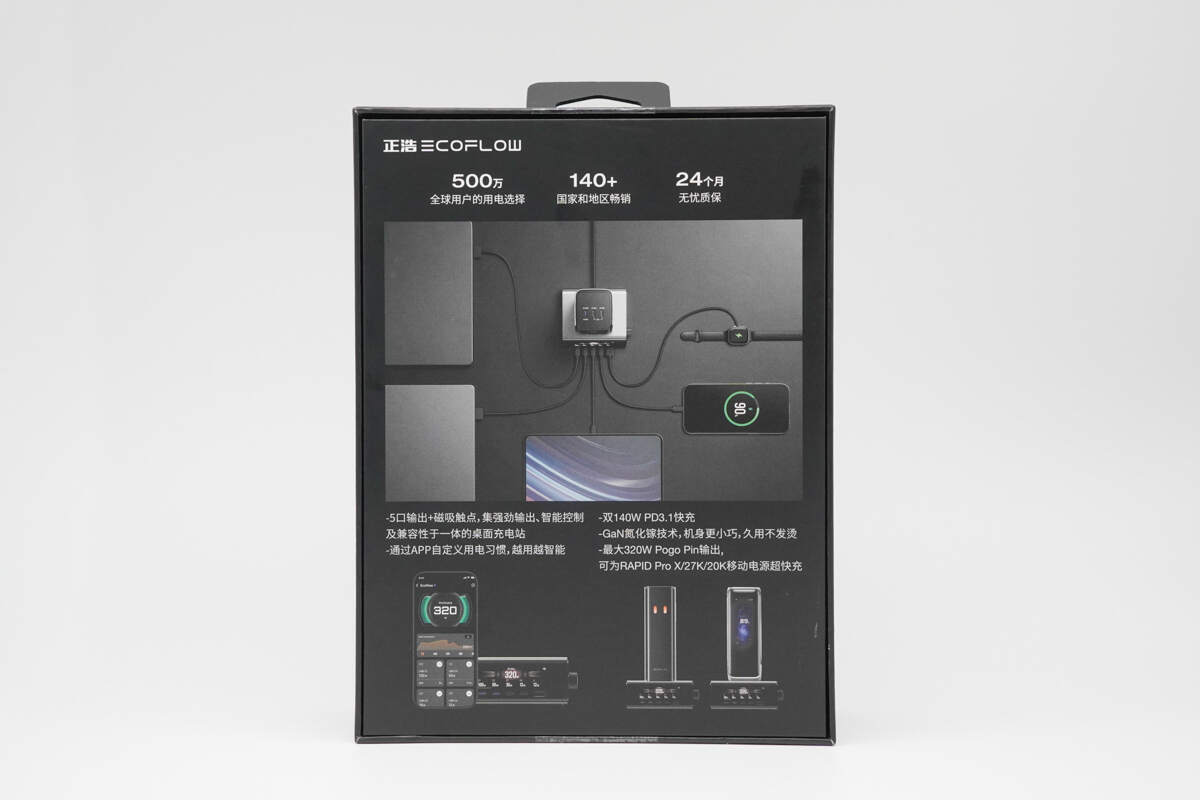
The back of the packaging displays the product’s usage scenarios and highlights its key features.
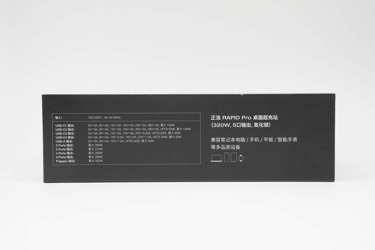
This side of the packaging displays the product specifications.
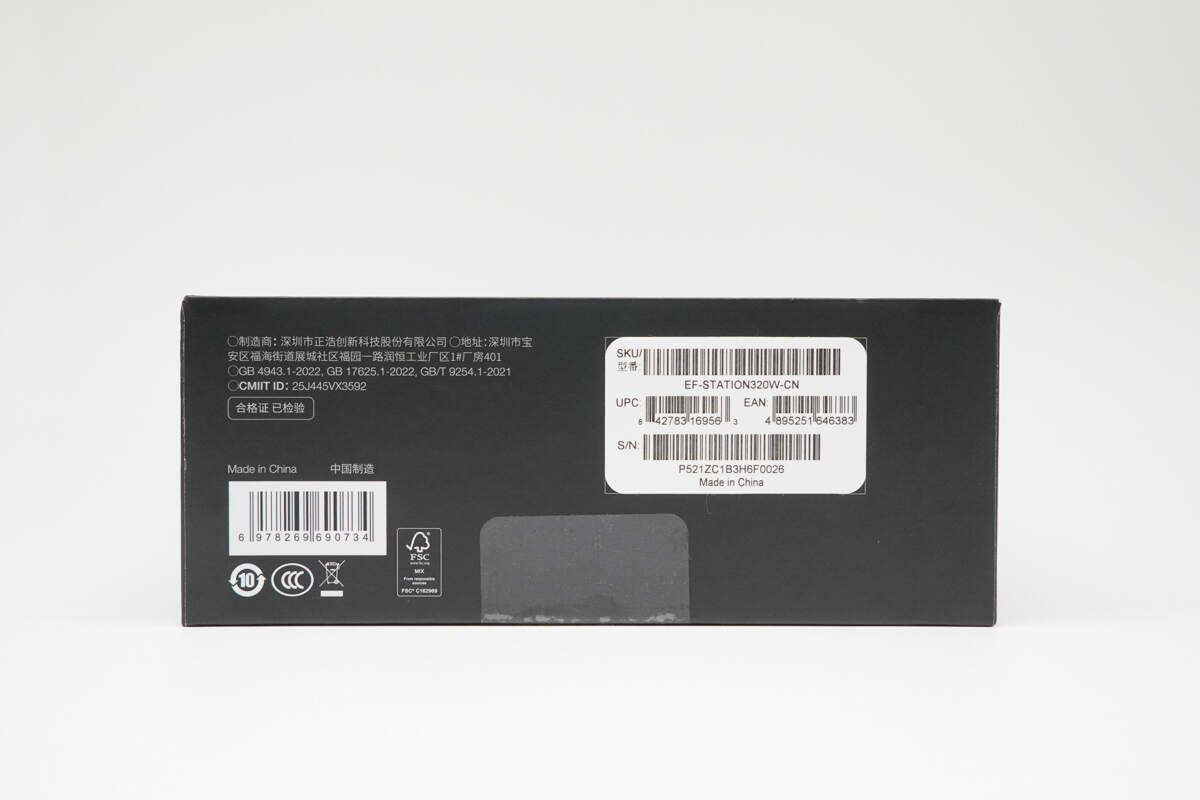
The bottom displays the manufacturer information and the serial number.

The package includes the desktop charger, a power cord, and a user manual.
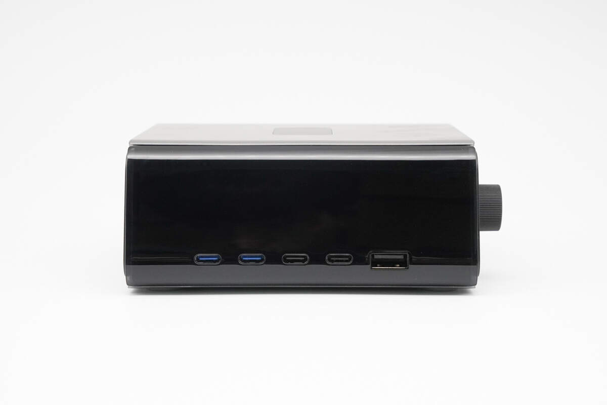
The front of the device features a display screen and multiple ports.
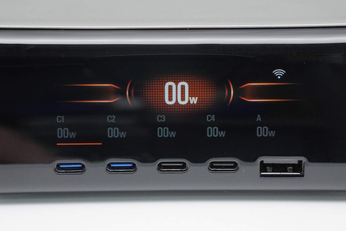
When powered on, the screen lights up and displays each port along with a total output power of 0W.
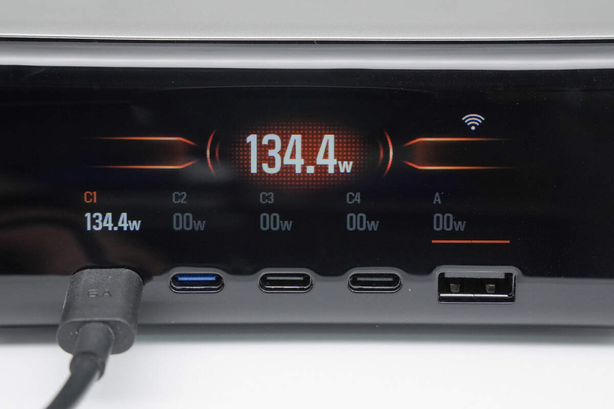
When a load is connected to the USB-C1 port, the screen displays the current output power of that port as well as the total output power.
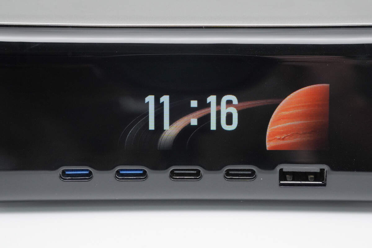
The screen displays the standby time interface.
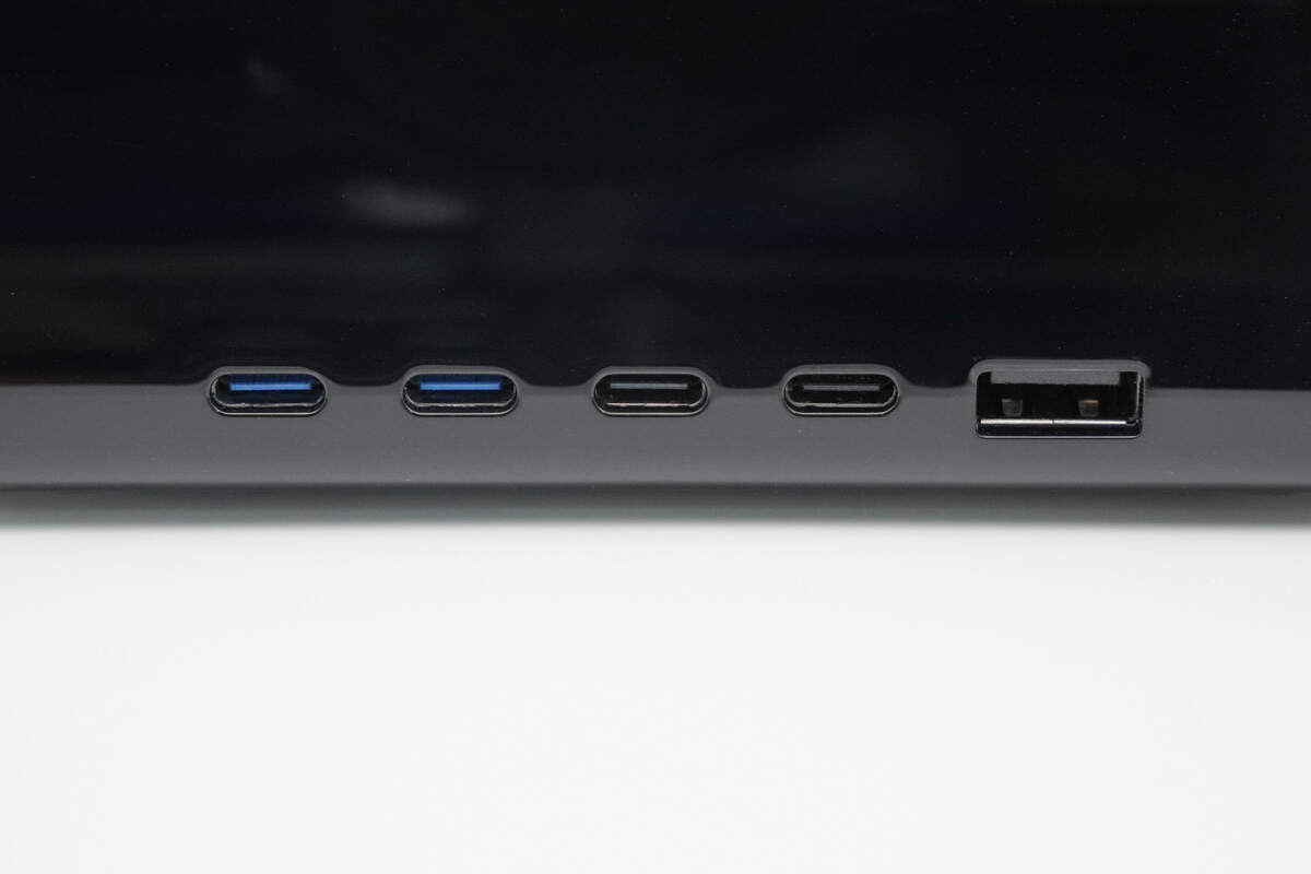
Below the screen are the USB ports.

The back of the device features a C7 power input socket.
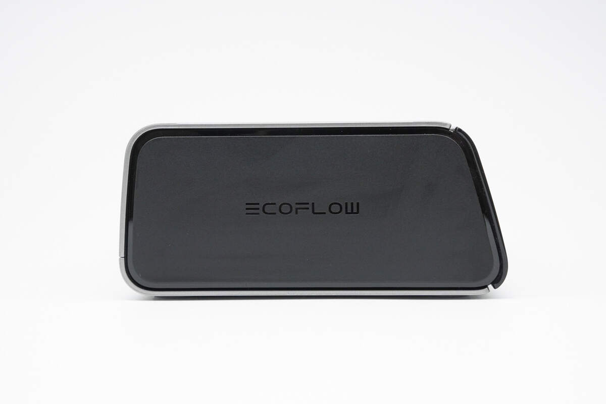
This side is printed with the ECOFLOW logo.
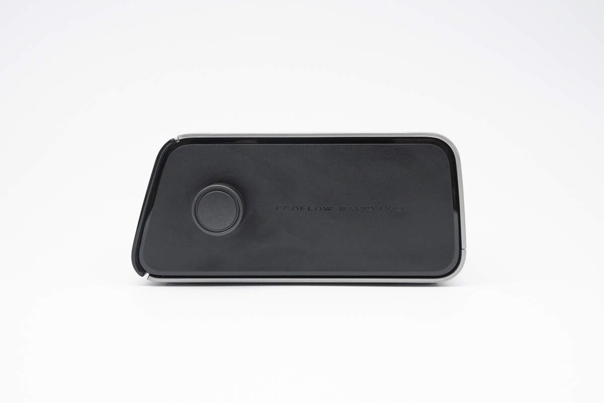
The other side features a rotary knob.

The rotary knob also supports pressing functionality.
The top features a POGO PIN magnetic connector.
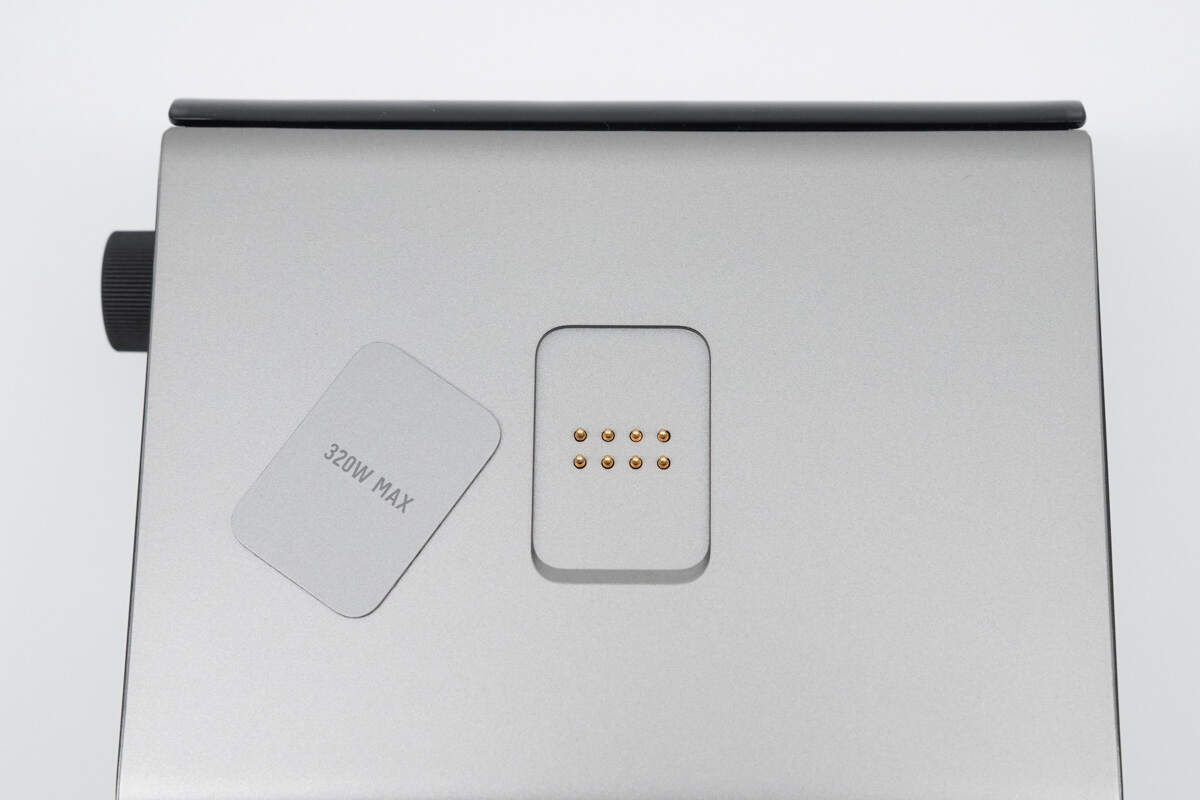
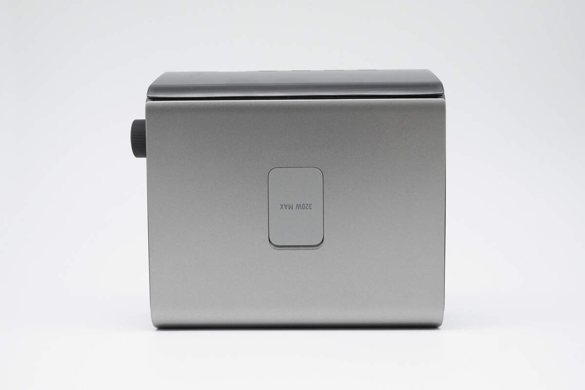
The protective cover is printed with “320W MAX,” indicating the maximum output power of the magnetic connector.
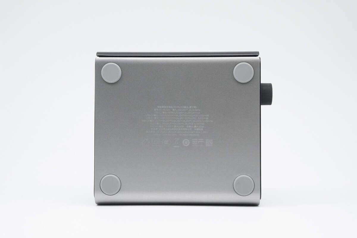
The bottom of the device displays the specifications and is equipped with anti-slip pads on four corners.
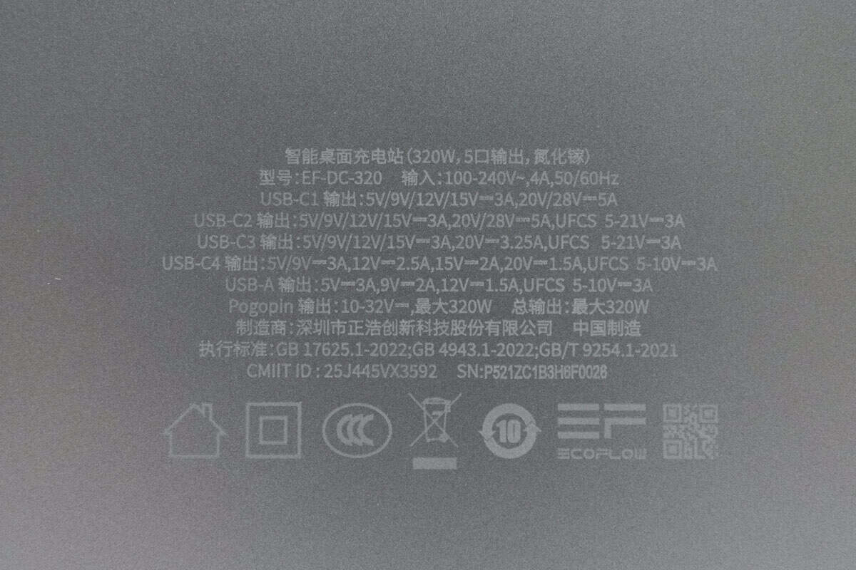
Model: EF-DC-320
Input: 100-240V~, 4A, 50/60Hz
USB-C1 Output: 5V/9V/12V/15V 3A, 20V/28V 5A
USB-C2 Output: 5V/9V/12V/15V 3A, 20V/28V 5A, UFCS 5-21V 3A
USB-C3 Output: 5V/9V/12V/15V 3A, 20V 3.25A, UFCS 5-21V 3A
USB-C4 Output: 5V/9V 3A, 12V 2.5A, 15V 2A, 20V 1.5A, UFCS 5-10V 3A
USB-A Output: 5V 3A, 9V 2A, 12V 1.5A, UFCS 5-10V 3A
PogoPin Output: 10-32V, 320W
Total Output: 320W
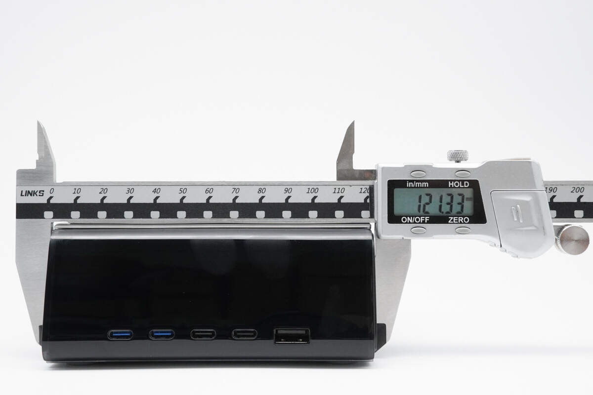
The length of the desktop charger is about 121.3 mm (4.78 inches).
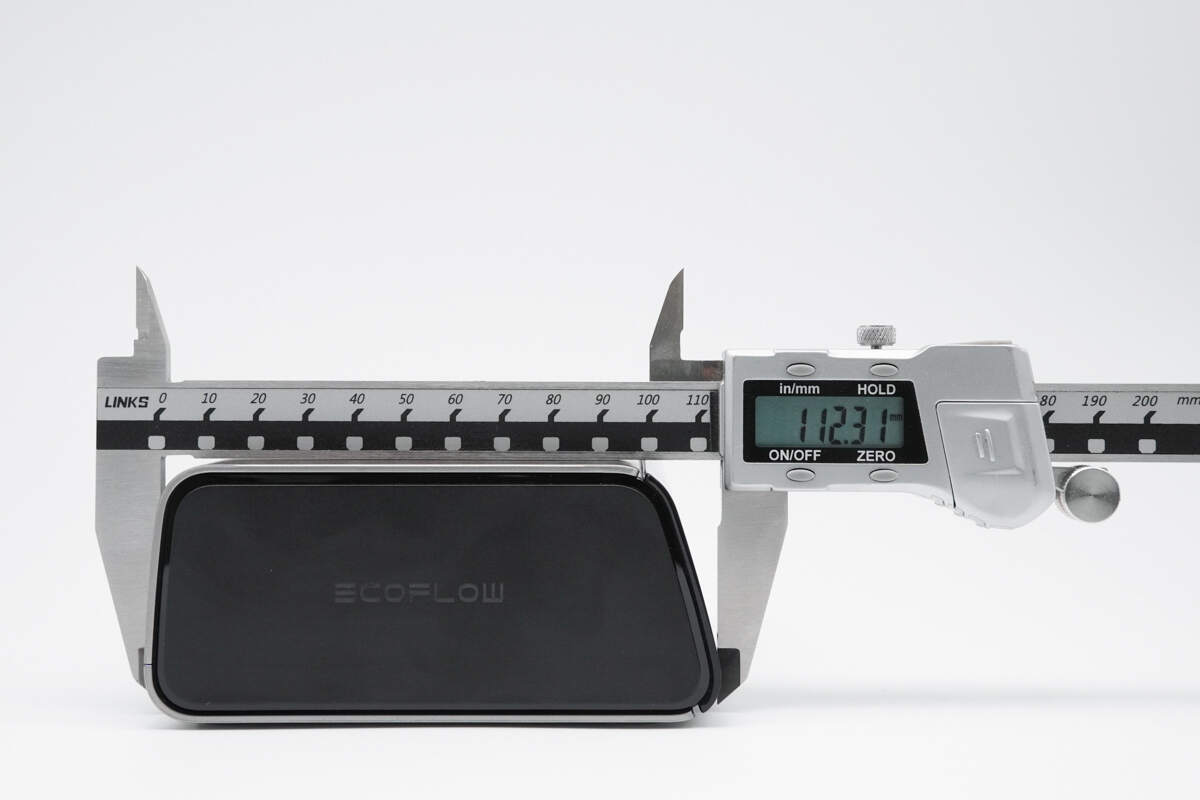
The width is about 112.3 mm (4.42 inches).
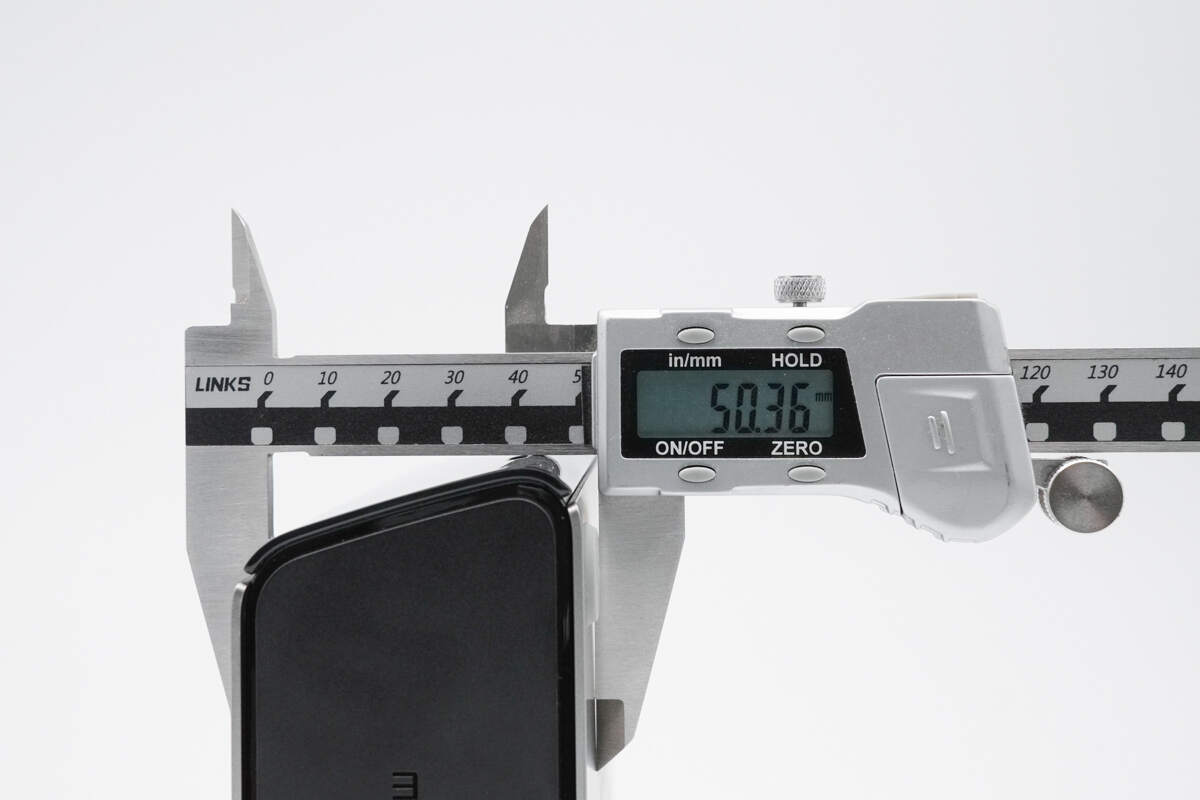
The height is about 50.4 mm (1.98 inches).
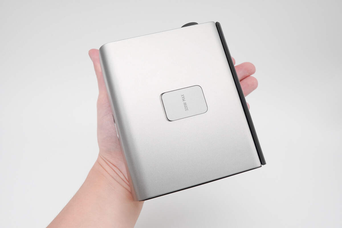
That's how big it is in the hand.
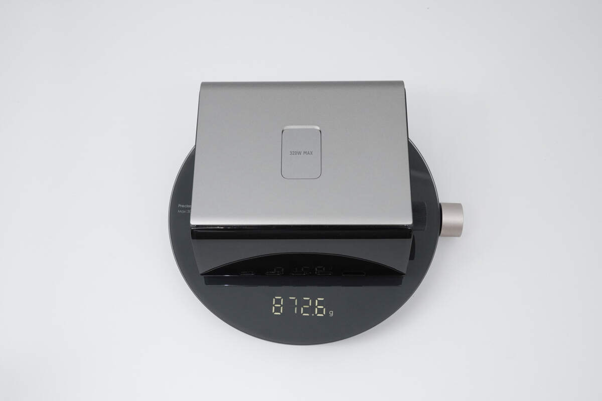
The weight is about 873 g (30.79 oz).
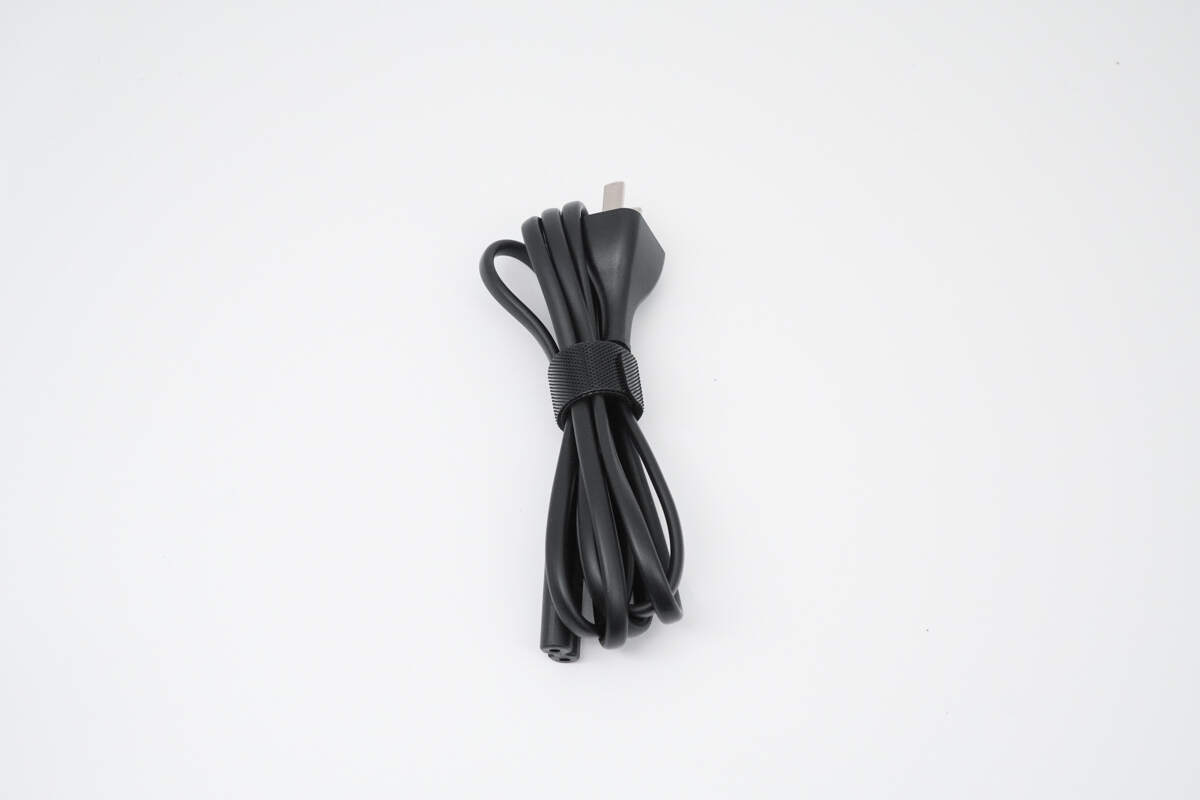
The power cord is secured with a Velcro strap.
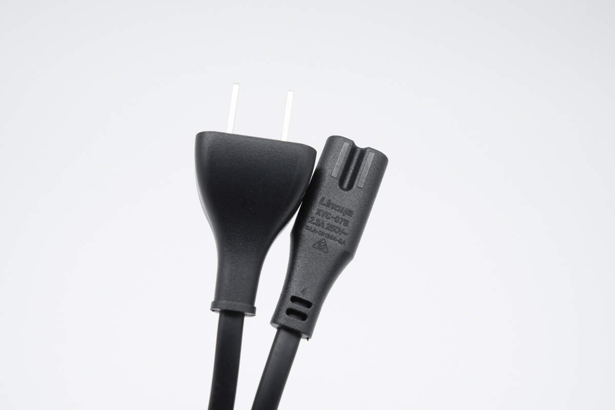
The power cord consists of two ends: a two-prong plug and a C7 connector.
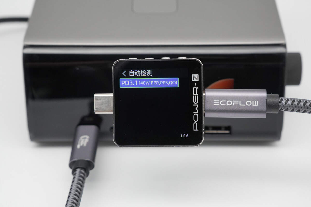
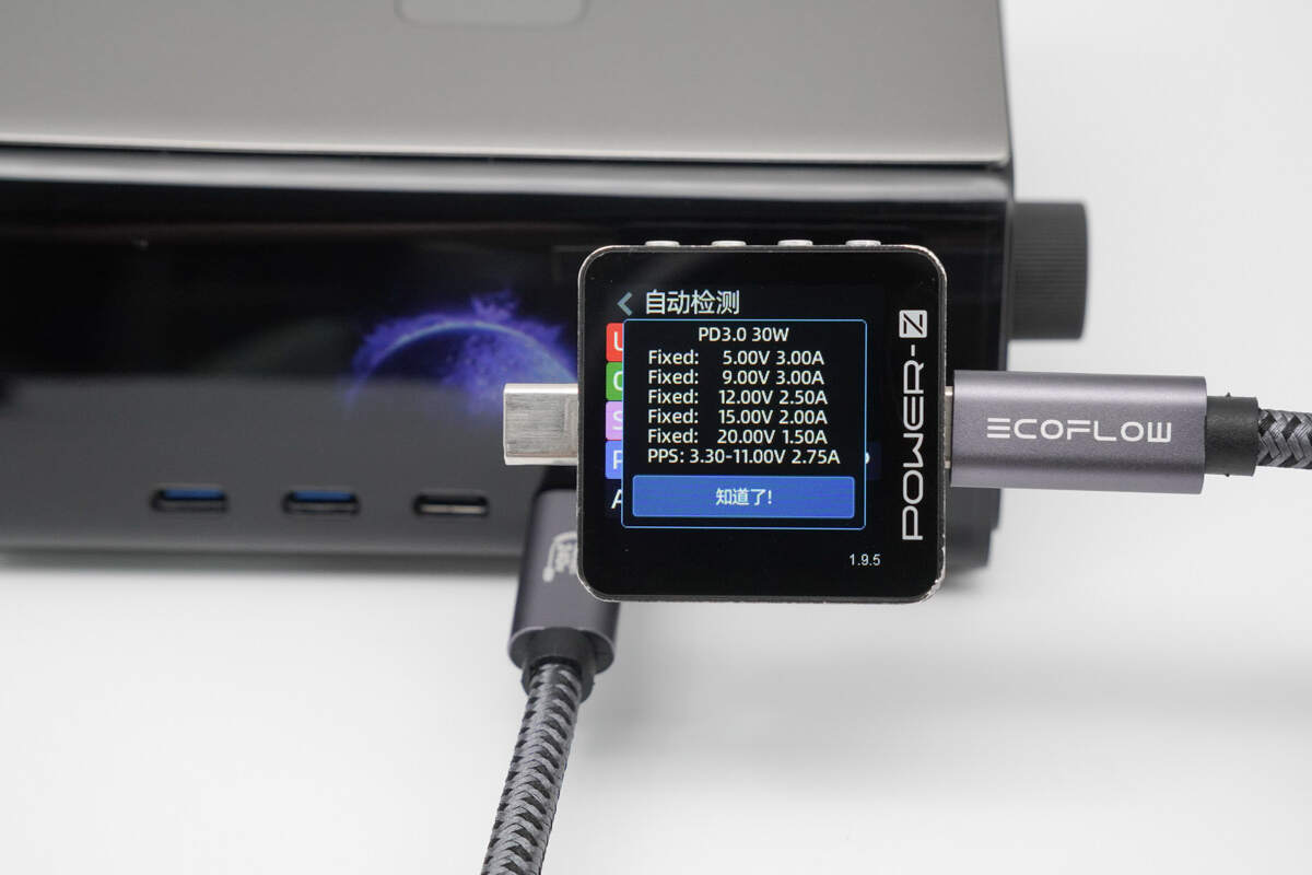
ChargerLAB POWER-Z KM003C shows that the USB-C1 supports PD3.1, PPS, and QC4 protocols.
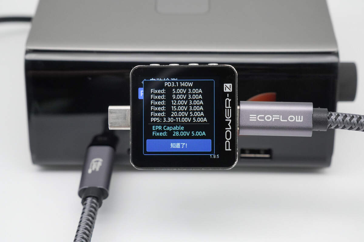
It has six fixed PDOs of 5V3A, 9V3A, 12V3A, 15V3A, 20V5A, and 28V5A. It also has one set of PPS, which is 3.3-11V5A.
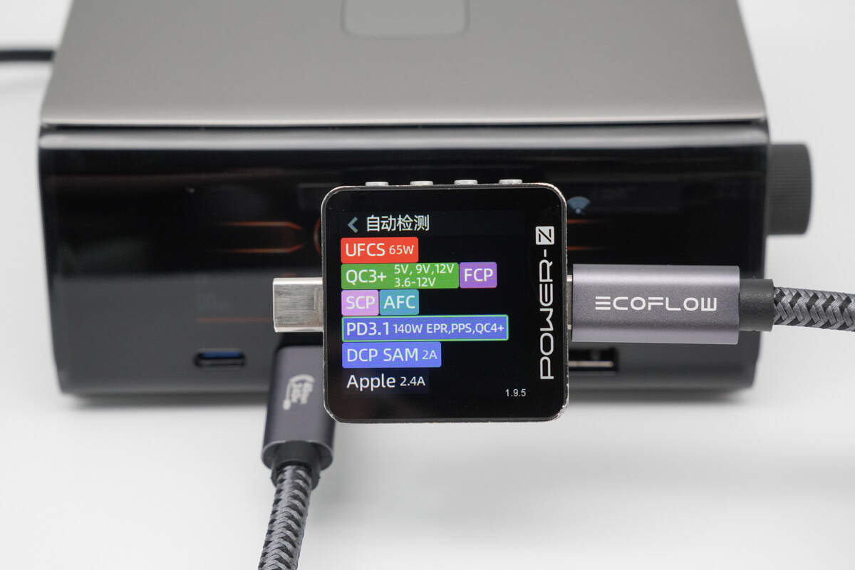
The USB-C2 supports UFCS, QC3+/4+, FCP, SCP, AFC, PD3.1, PPS, DCP, SAM 2A, and Apple 2.4A protocols.

The PDO profile is identical to that of the USB-C1 port.
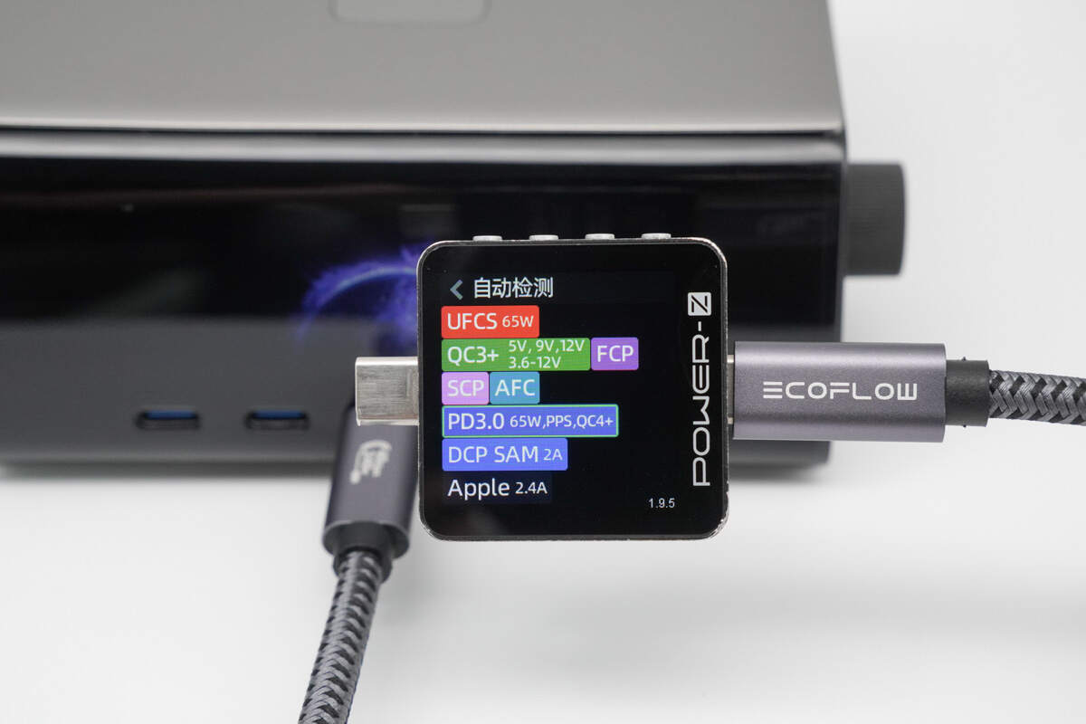
The USB-C3 supports UFCS, QC3+/4+, FCP, SCP, AFC, PD3.0, PPS, DCP, SAM 2A, and Apple 2.4A protocols.
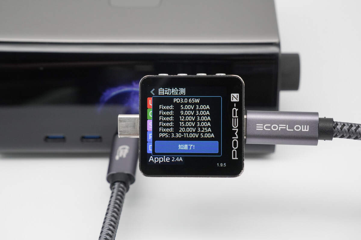
It has five fixed PDOs of 5V3A, 9V3A, 12V3A, 15V3A, and 20V3.25A. It also has one set of PPS, which is 3.3-11V5A.
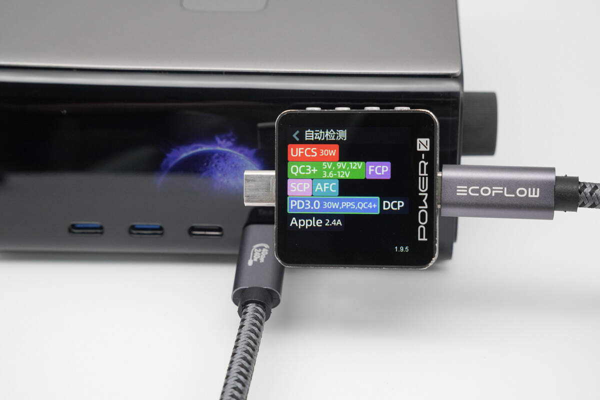
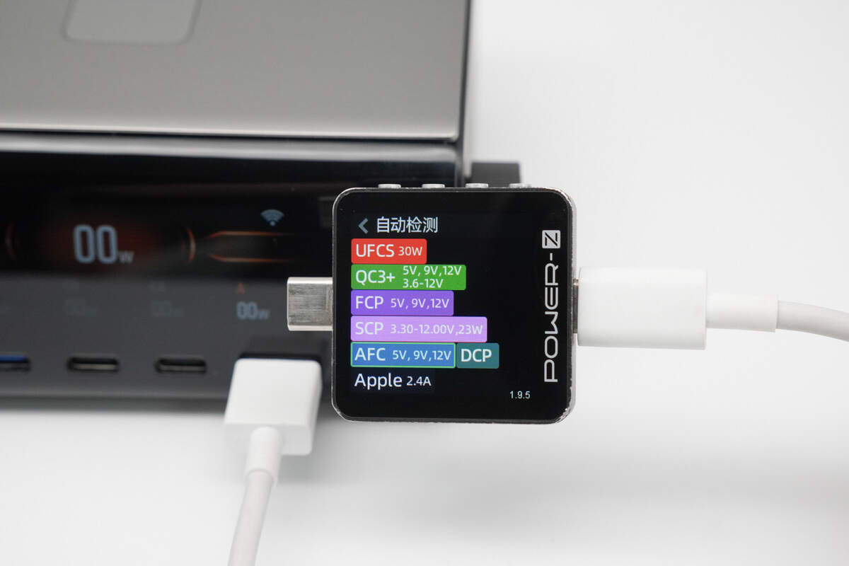
The USB-C4 supports UFCS, QC3+/4+, FCP, SCP, AFC, PD3.0, PPS, DCP, and Apple 2.4A protocols.
It has five fixed PDOs of 5V3A, 9V3A, 12V2.5A, 15V2A, and 20V1.5A. It also has one set of PPS, which is 3.3-11V2.75A.
The USB-A supports UFCS, QC3+, FCP, SCP, AFC, DCP, and Apple 2.4A protocols.
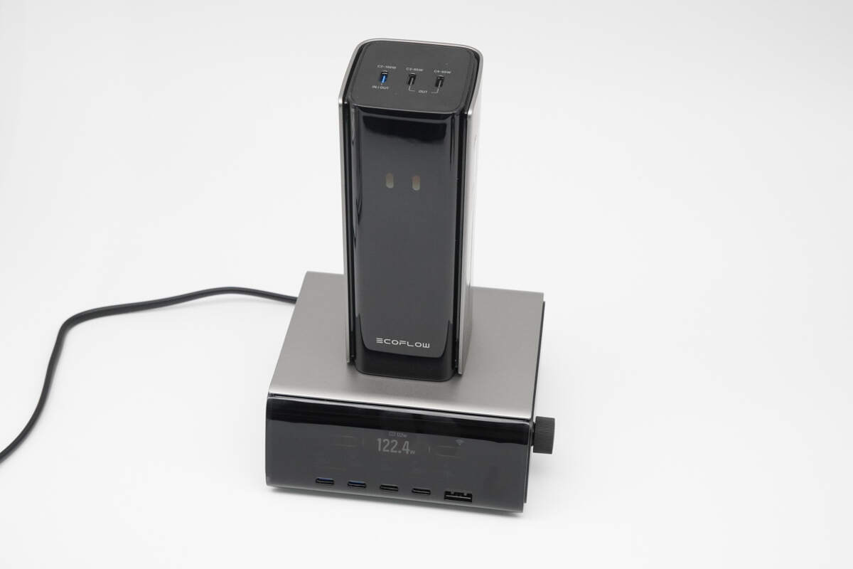
Use the PogoPin contacts on the top of the desktop charger to charge an EcoFlow portable power station.
The screen shows the charging power is 122.4W.

Charging the EcoFlow portable power station via the USB-C1 port shows a charging power of 136W.
Teardown
Next, let's take it apart to see its internal components and structure.
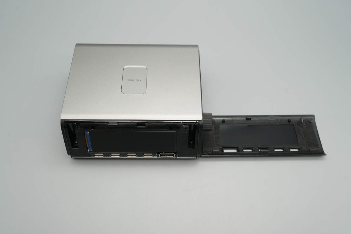
Pry open the front panel.

There are mounting screws located on both sides of the screen.
Unscrew the mounting screws to open the enclosure.
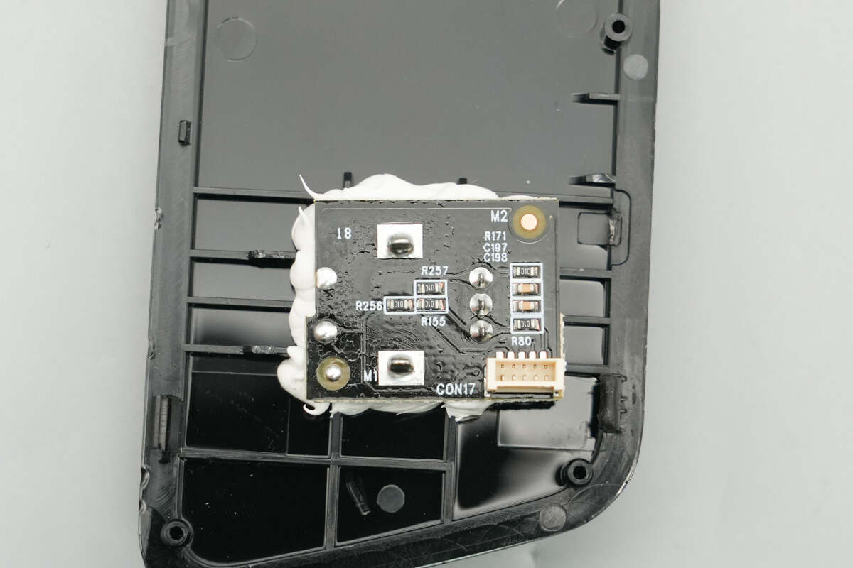
The side panel is secured with clips and contains the PCB for the rotary knob.
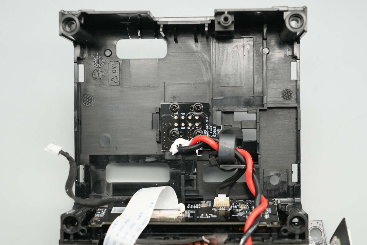
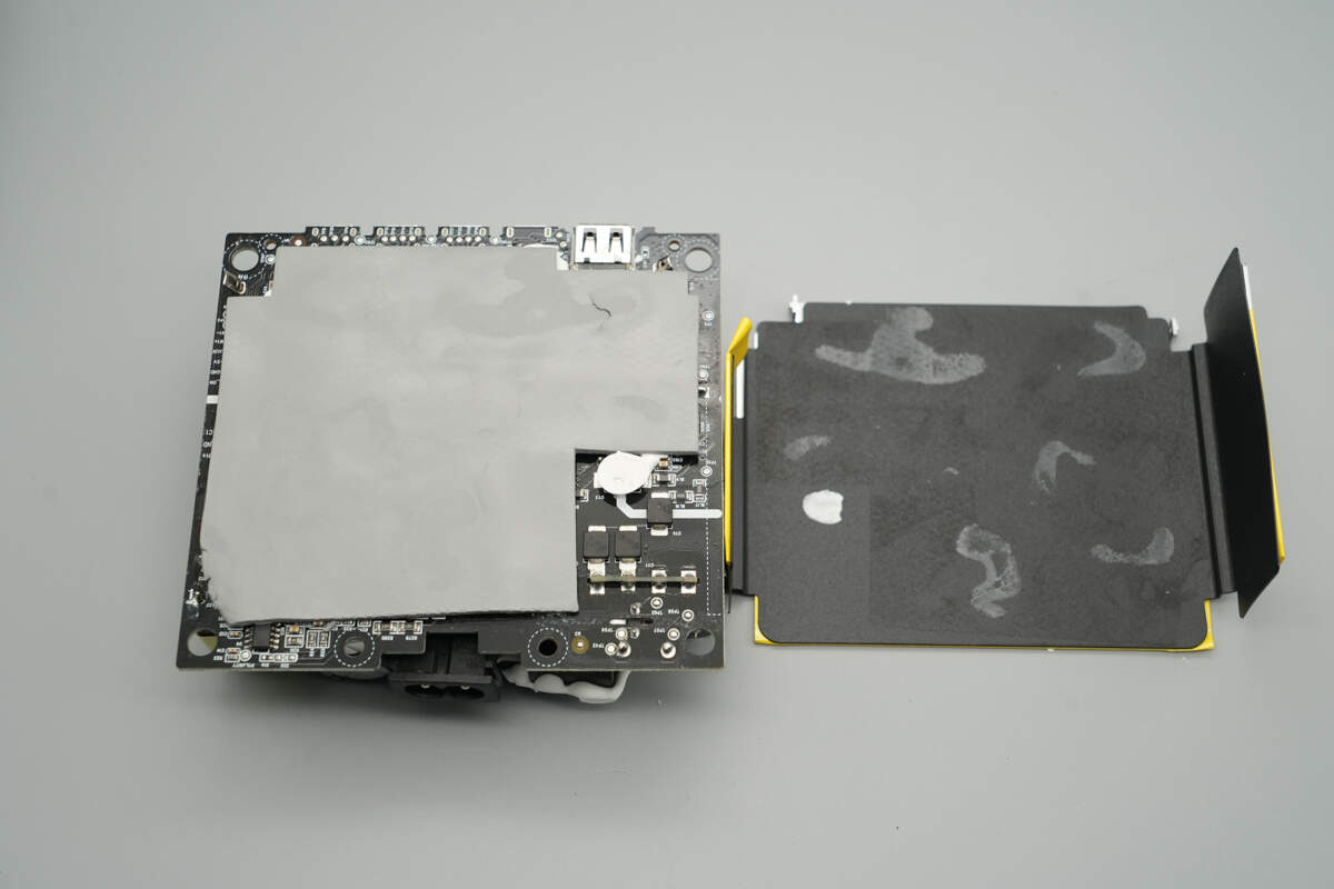
The PogoPin contact PCB is connected via wires, while the display PCB is connected via a ribbon cable.
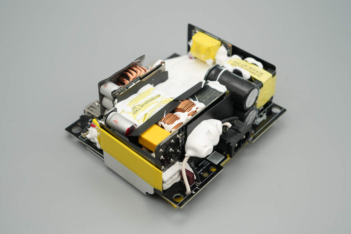
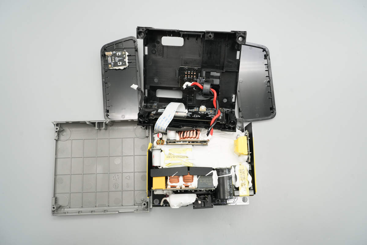
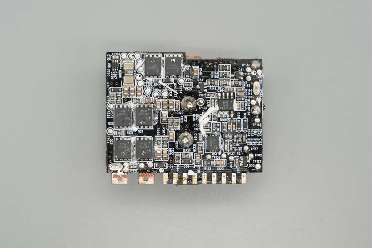
The PCBA module uses multiple small PCBs soldered vertically to save space.
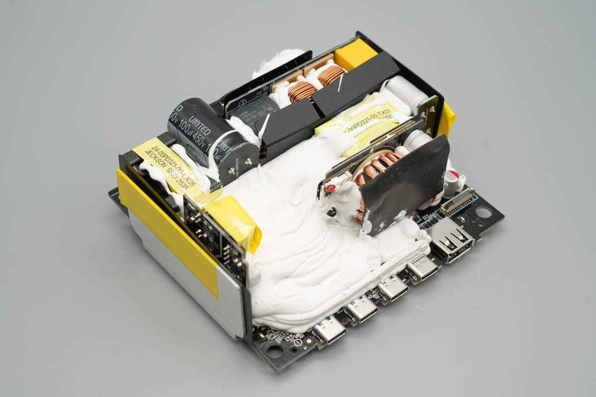
Mylar sheets are placed between the small PCBs for insulation, and adhesive is applied for structural reinforcement and protection.
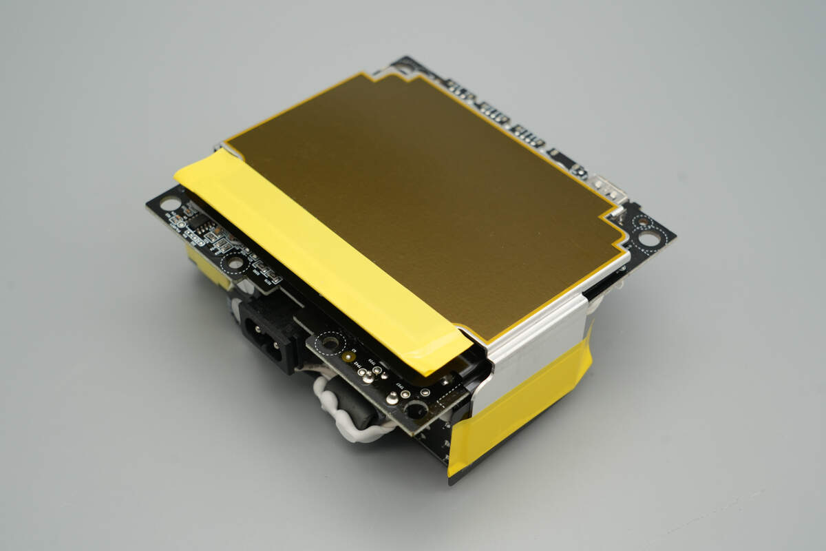
The back of the PCBA module is covered by an aluminum alloy heat sink, insulated with Mylar sheets.
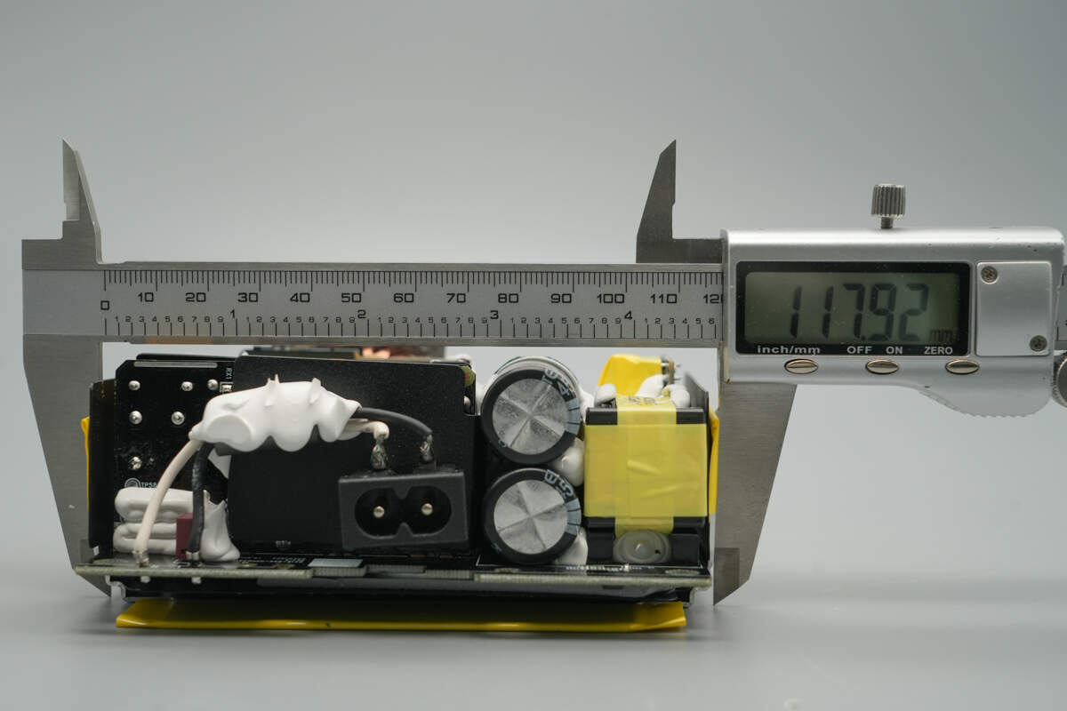
The length of the PCBA module is about 117.9 mm (4.64 inches).
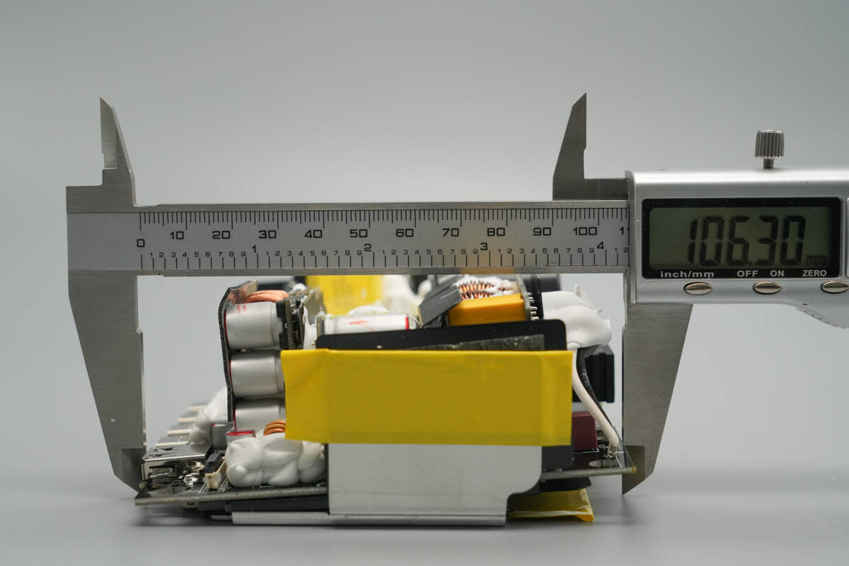
The width is about 106.3 mm (4.19 inches).
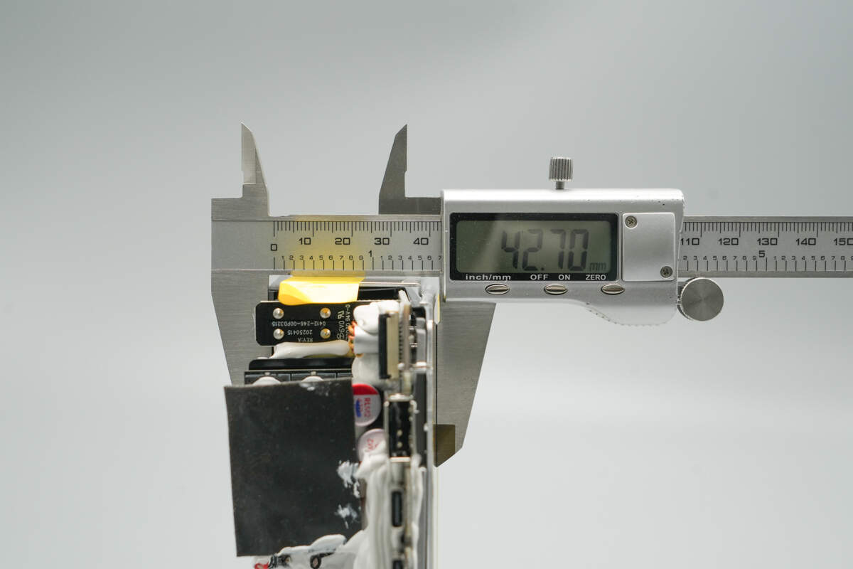
The thickness is about 42.7 mm (1.68 inches).
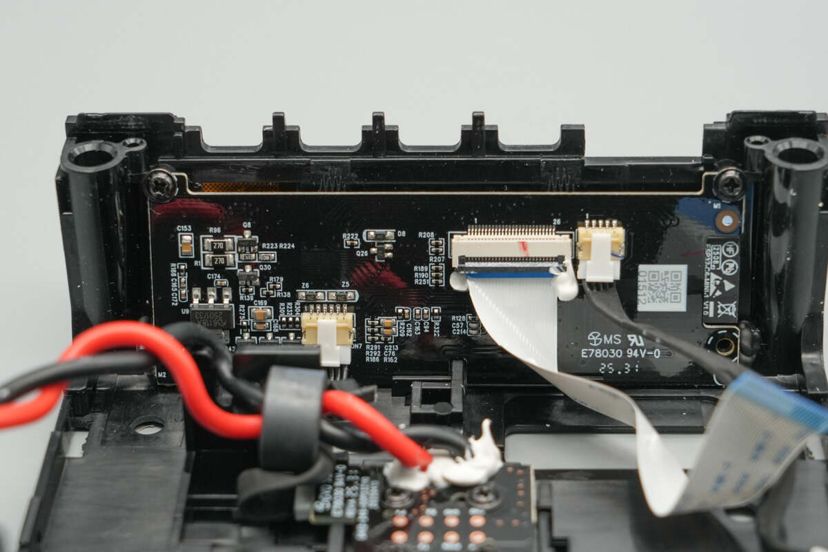
The display PCB is secured with screws, with a ribbon cable attached on the back.
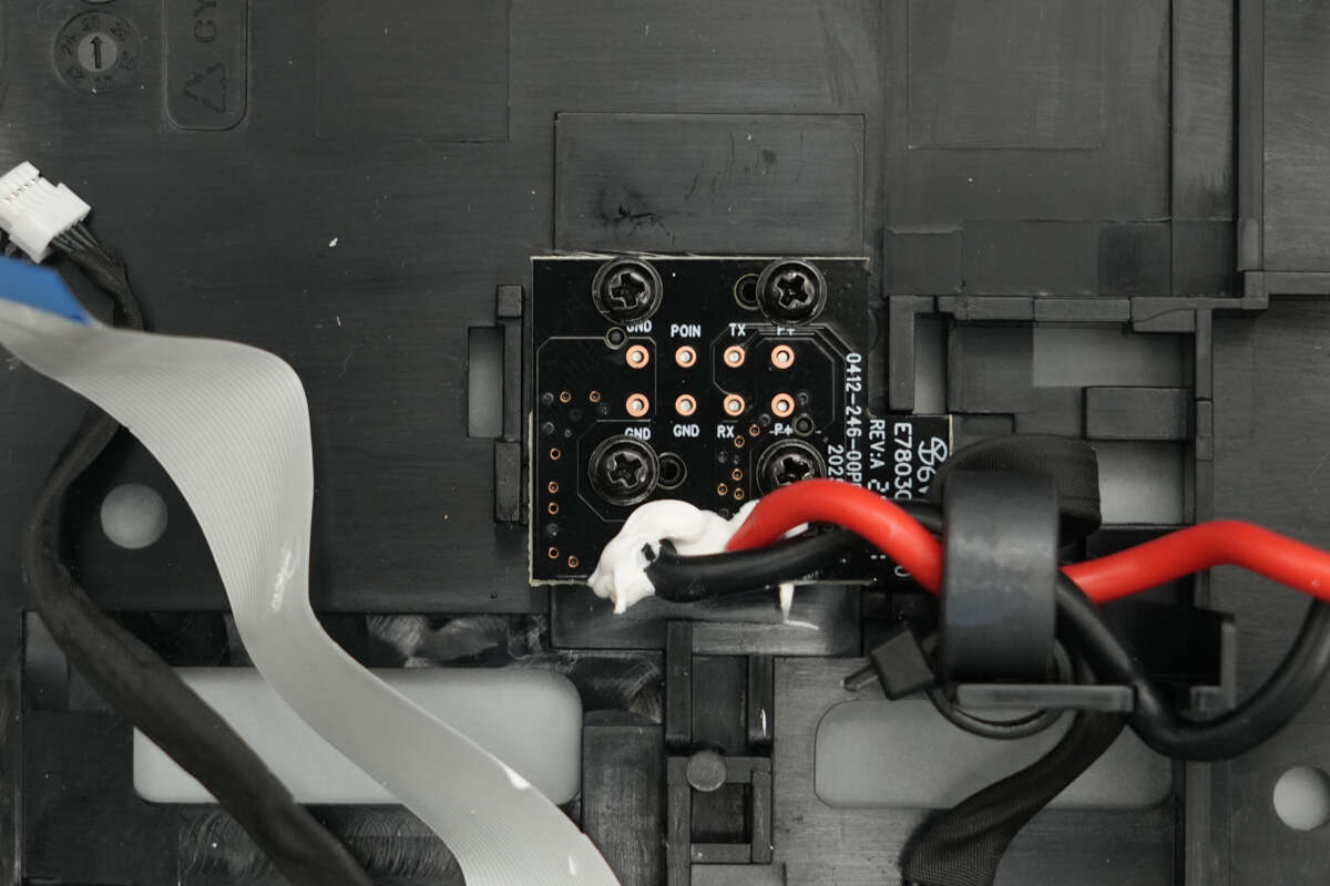
The PogoPin PCB is also secured with screws.
Remove the heat sink. The back of the PCBA module has a thermal pad for heat dissipation.

The front side of the PCBA module features components such as the PFC boost inductor, capacitors, auxiliary power PCB, LLC resonant capacitor, resonant inductor, LLC transformer, buck inductors, and buck converter PCB.
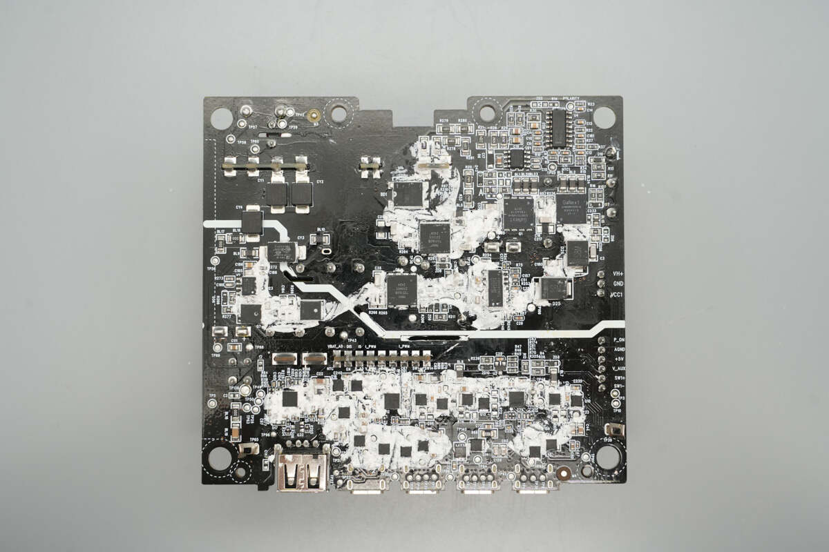
The back side houses components including the PFC controller, half-bridge driver, PFC MOSFETs, synchronous rectifiers, LLC controller, LLC MOSFETs, synchronous rectifier controller, synchronous buck chip, and buck MOSFETs.
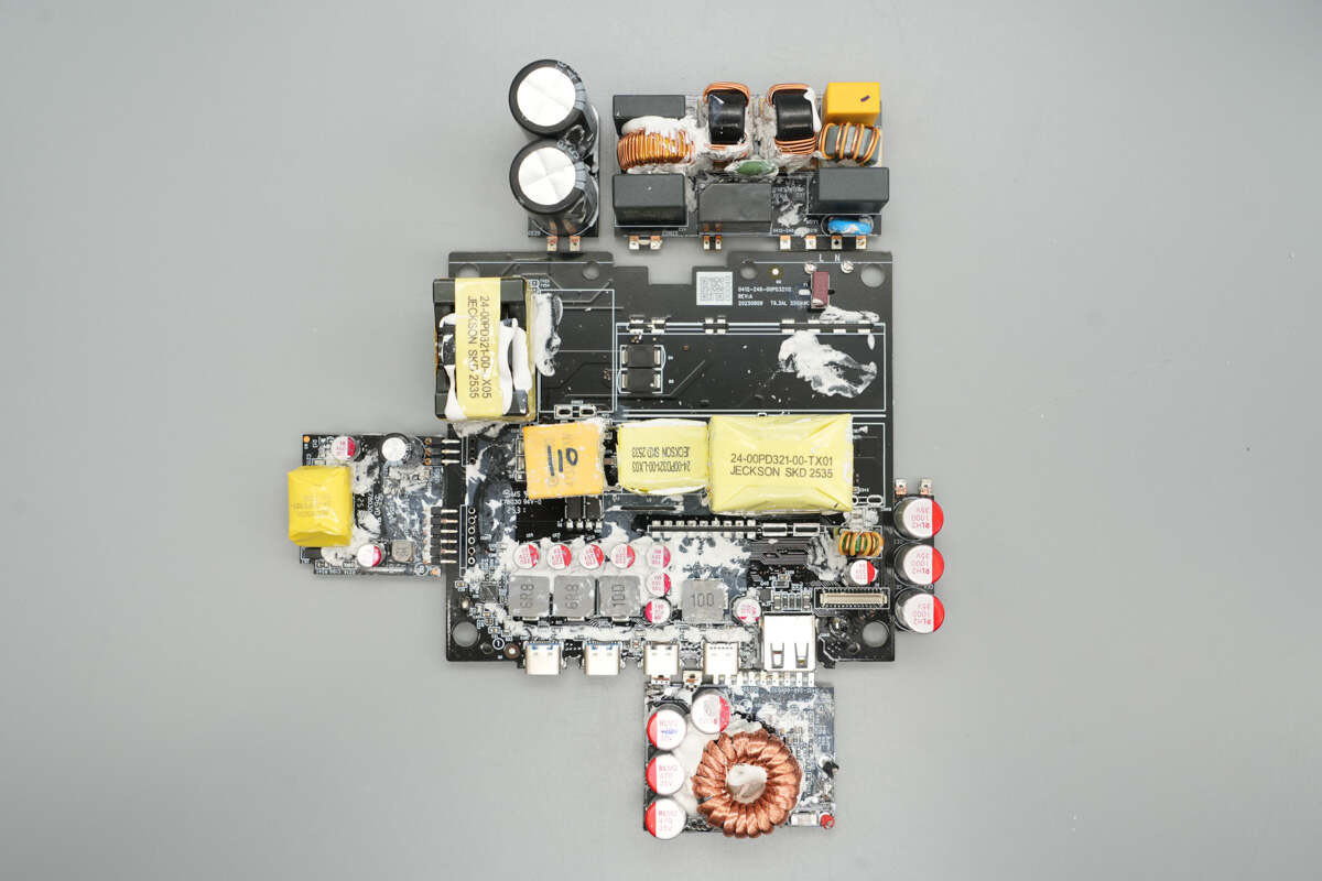
Remove the small PCBs.
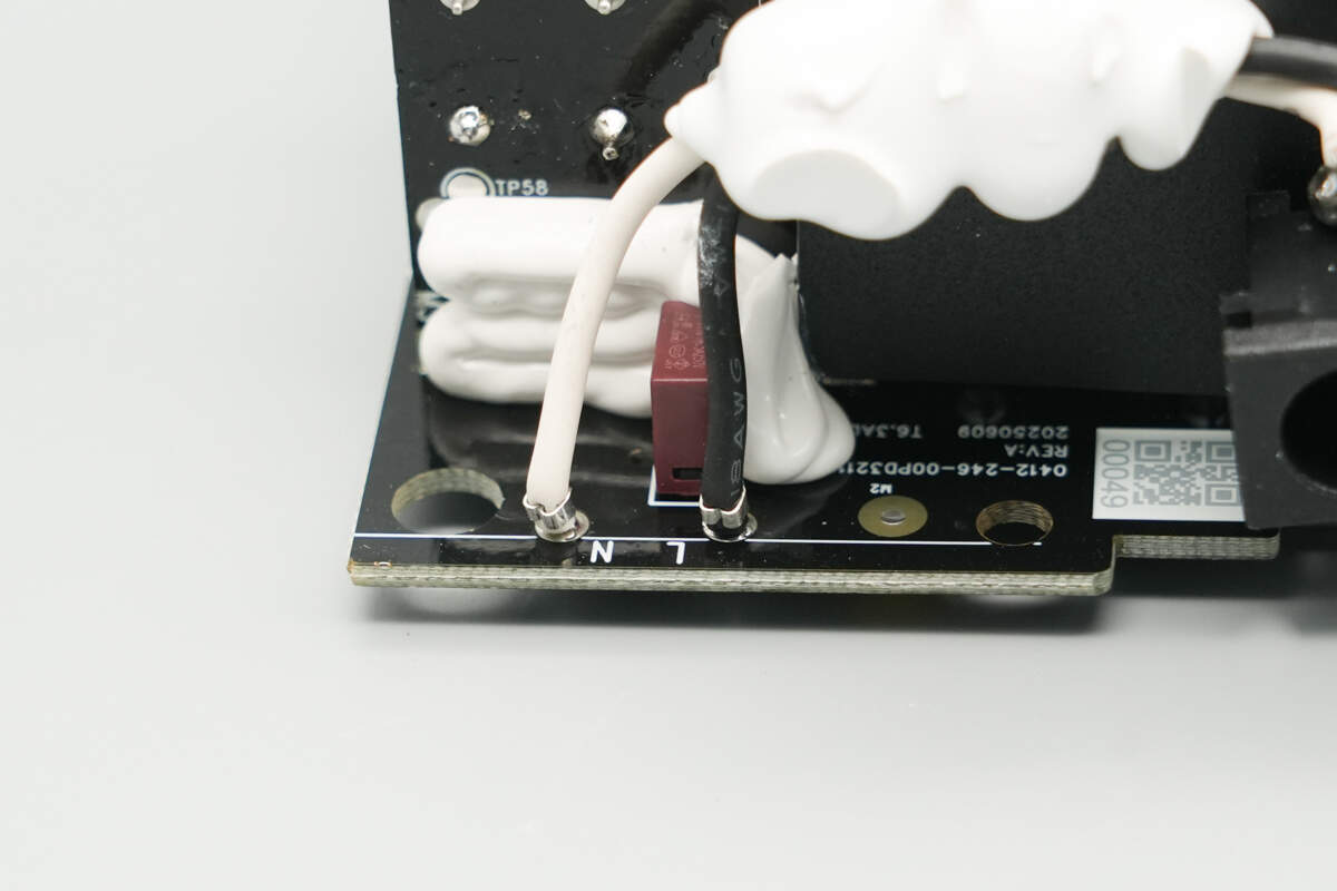
The input wires are connected via soldering.
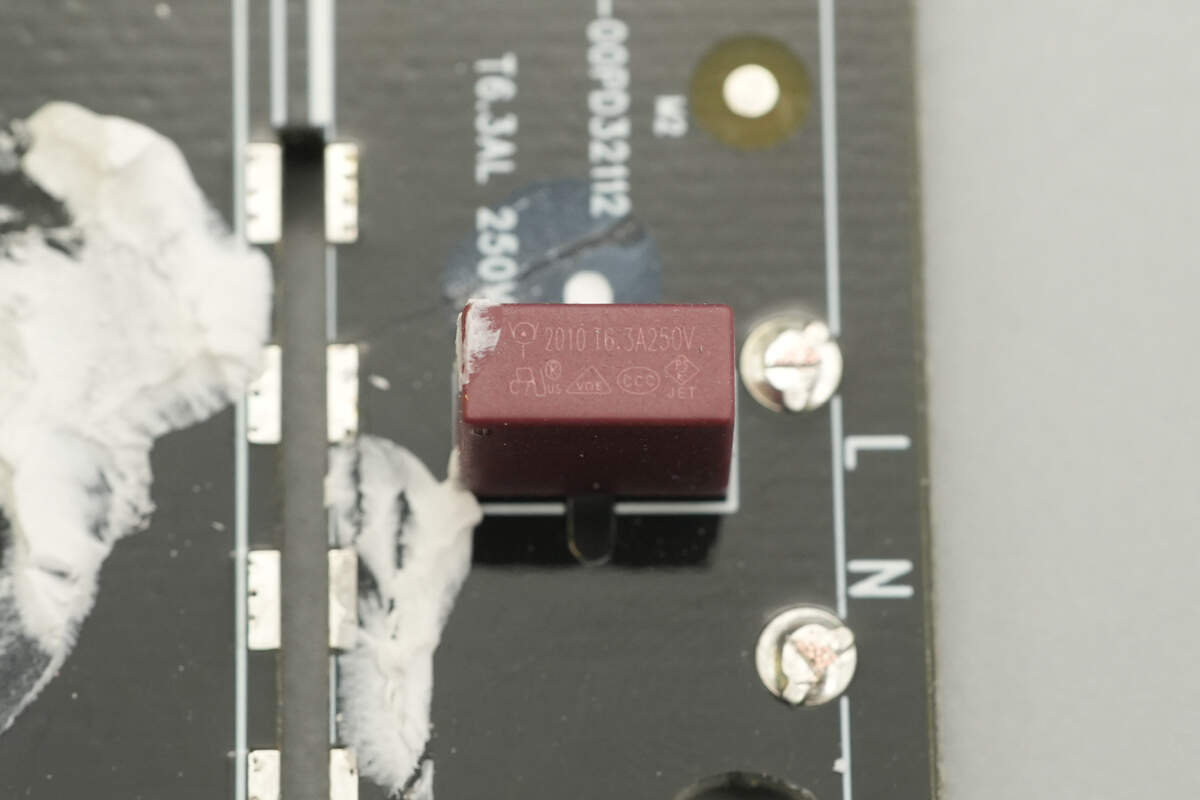
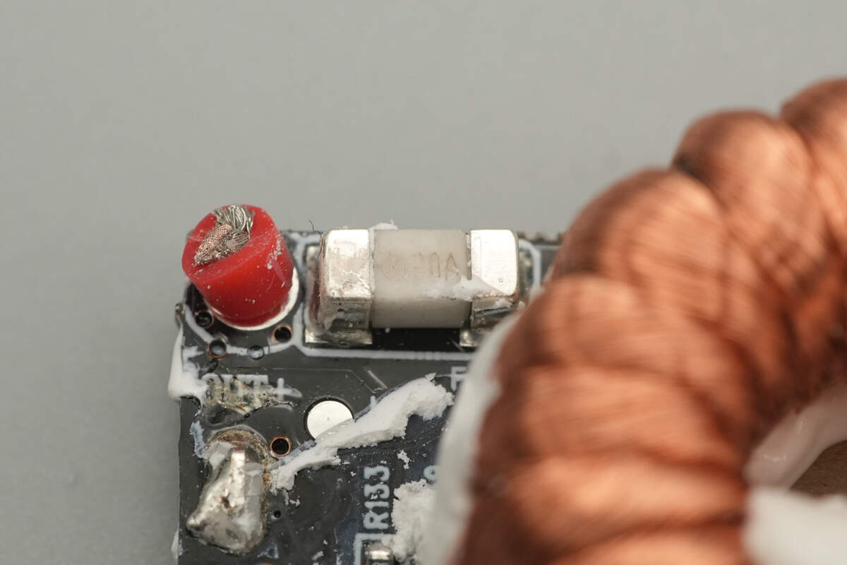
The fuse is from WalterFuse, rated at 6.3A 250V.
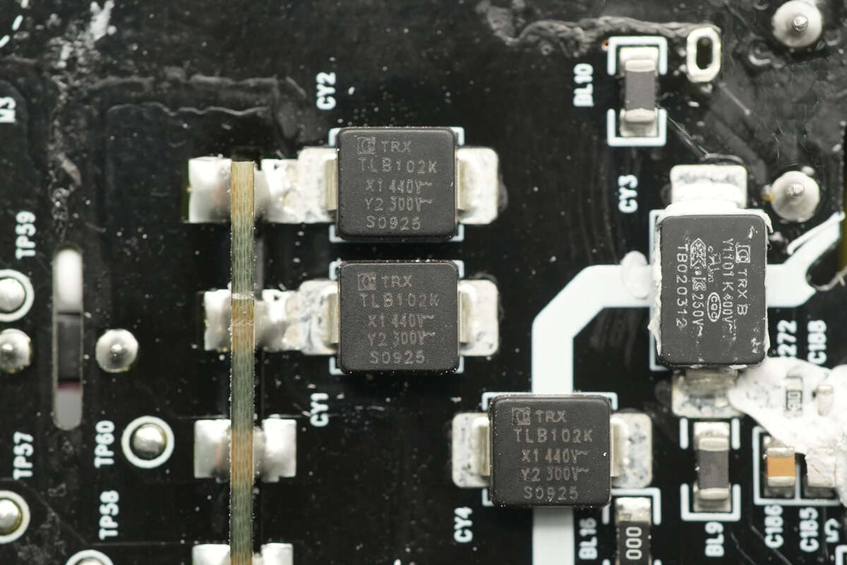
The SMD Y capacitors are from TRX. Their compact size and light weight make them ideal for high-density power products like GaN fast chargers. All three units share the part number TAY2102KB.
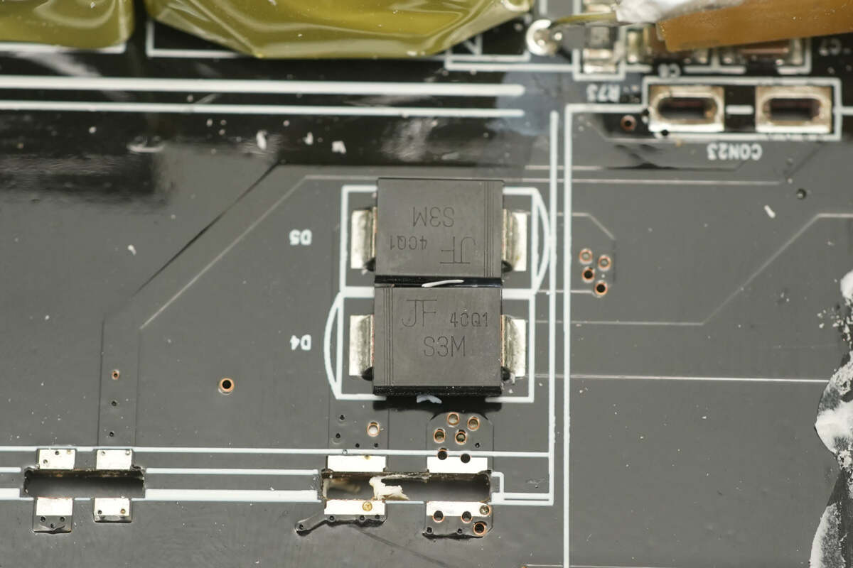
Two rectifiers are from JF, model S3M, using SMC packaging.
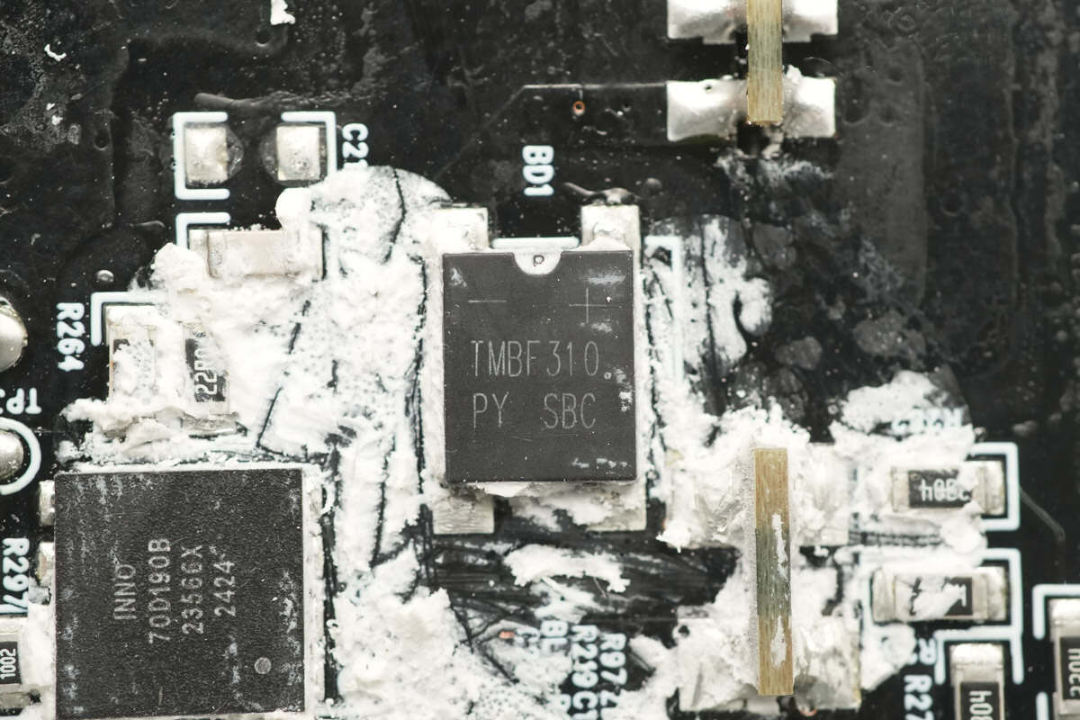
The bridge rectifier is from PY, model TMBF310, rated at 3A 1000V, and comes in a TMBF package.
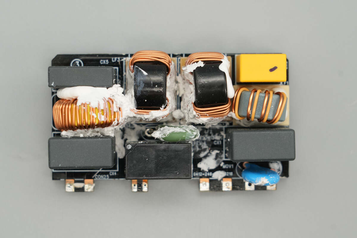
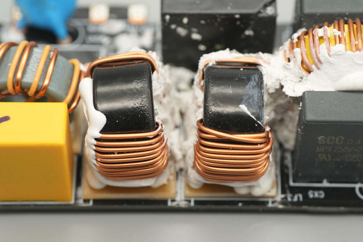
The filter PCB includes components such as a varistor, safety X2 capacitors, common mode chokes, a relay, and a filter inductor.
There are X-capacitor discharge resistors on the back.
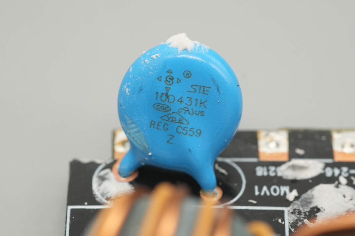
The input-side varistor is from STE, model 10D431K.
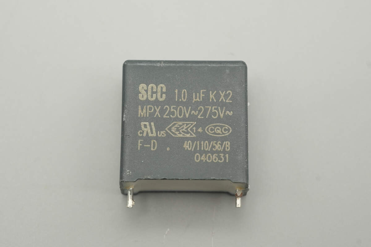
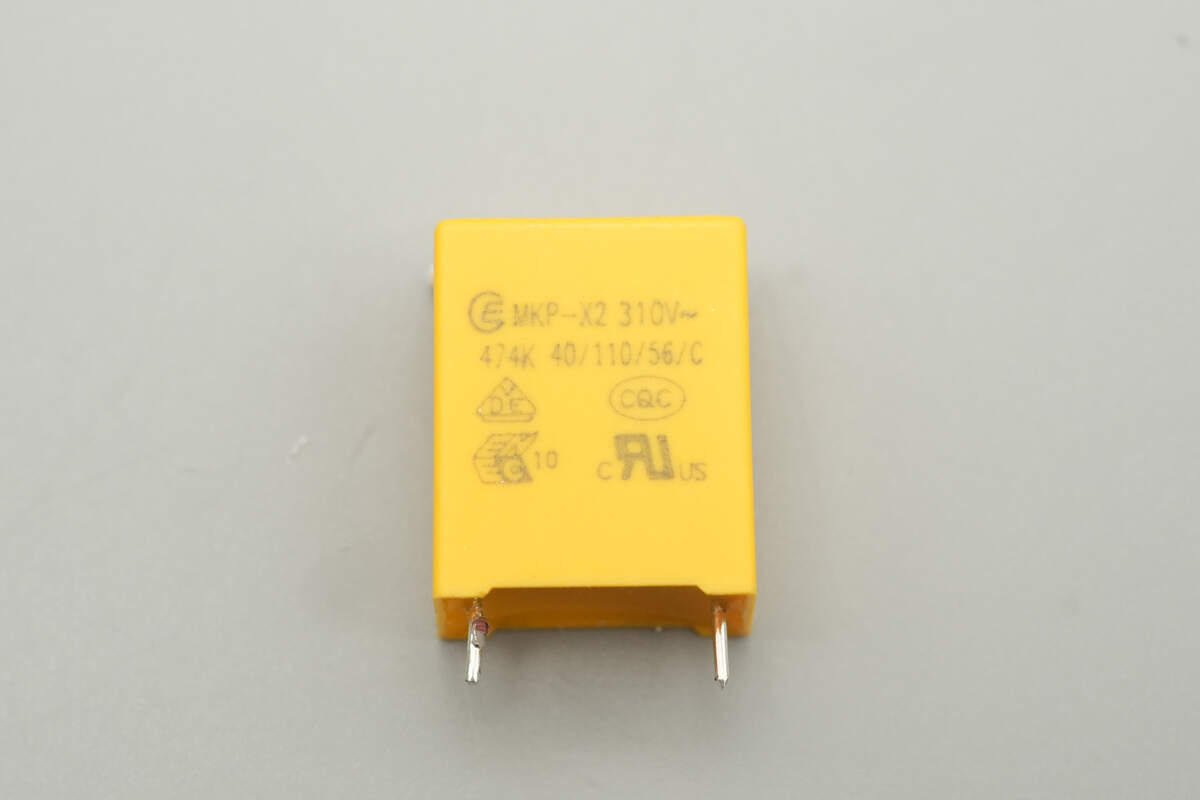
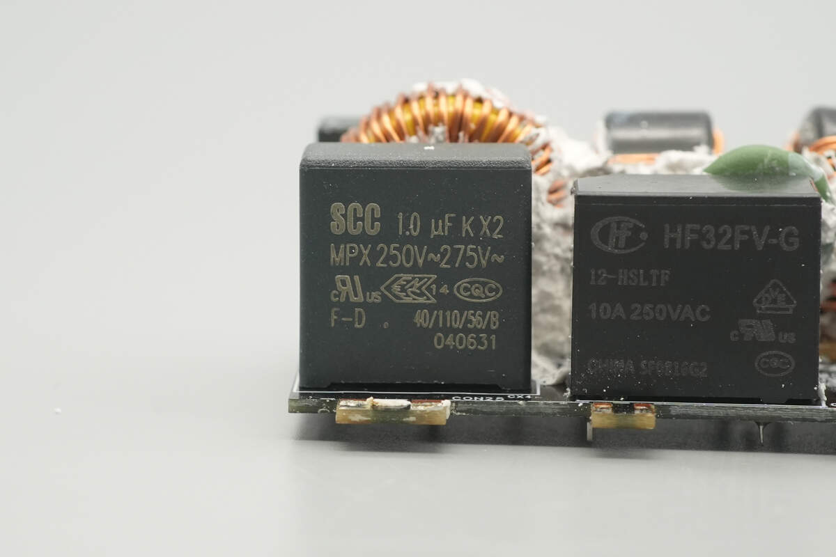
The safety X2 capacitor is supplied by SCC, with a specification of 1 μF.
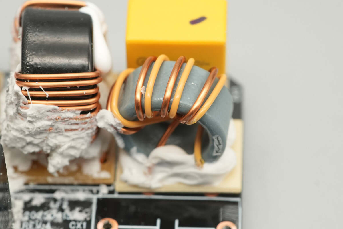
The common mode choke is wound with enameled wire and insulated wire, with a phenolic board installed at the bottom for insulation.
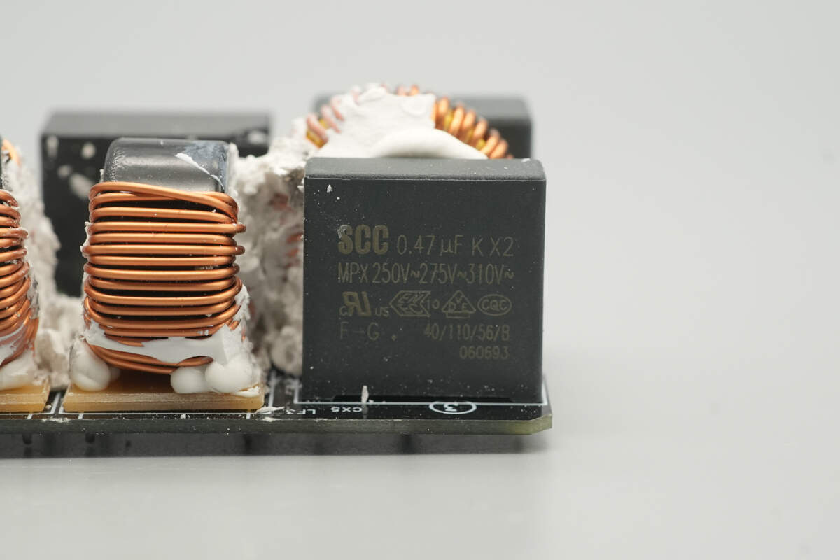
The safety X2 capacitor is sourced from EasyGather, with a specification of 0.47 μF.
Two common mode chokes are wound with enameled wire and feature phenolic board insulation at the bottom.
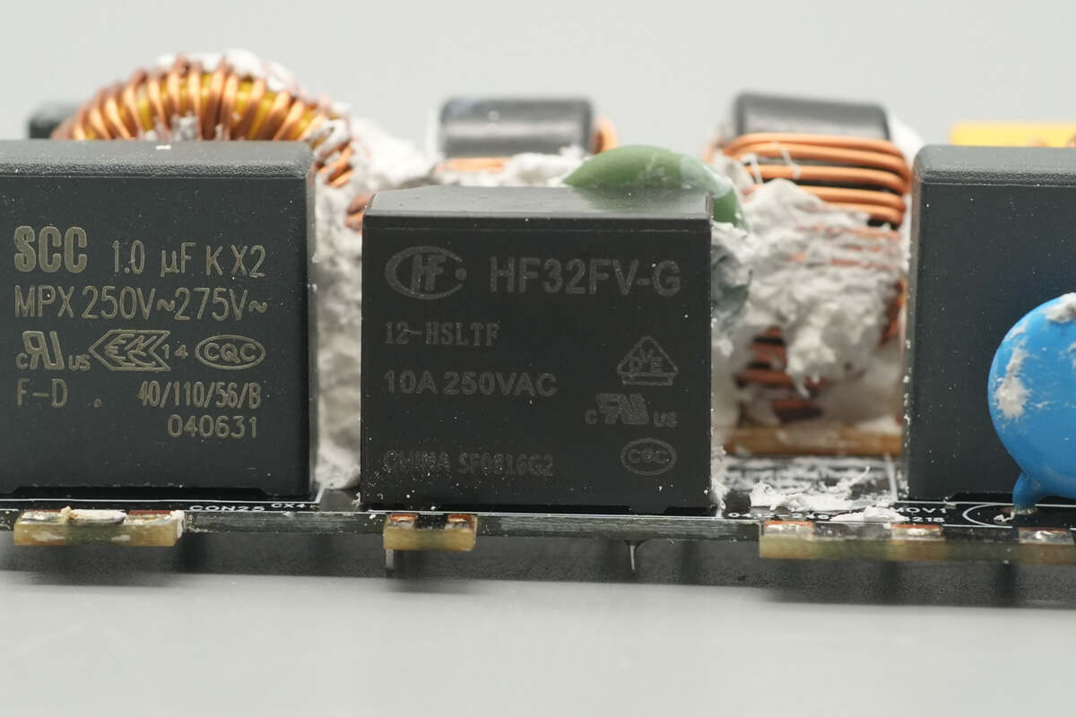
The relay is from HONGFA, model HF32FV-G/12-HSLTF. It is an ultra-compact medium-power relay with a contact rating of 10A and a coil voltage of 12V.
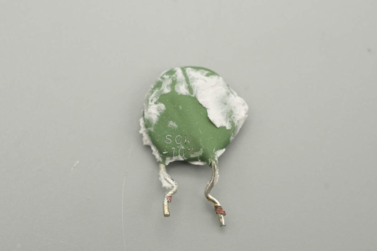
The NTC thermistor is marked with SCK 104.
The safety X2 capacitor has a specification of 0.47 μF.
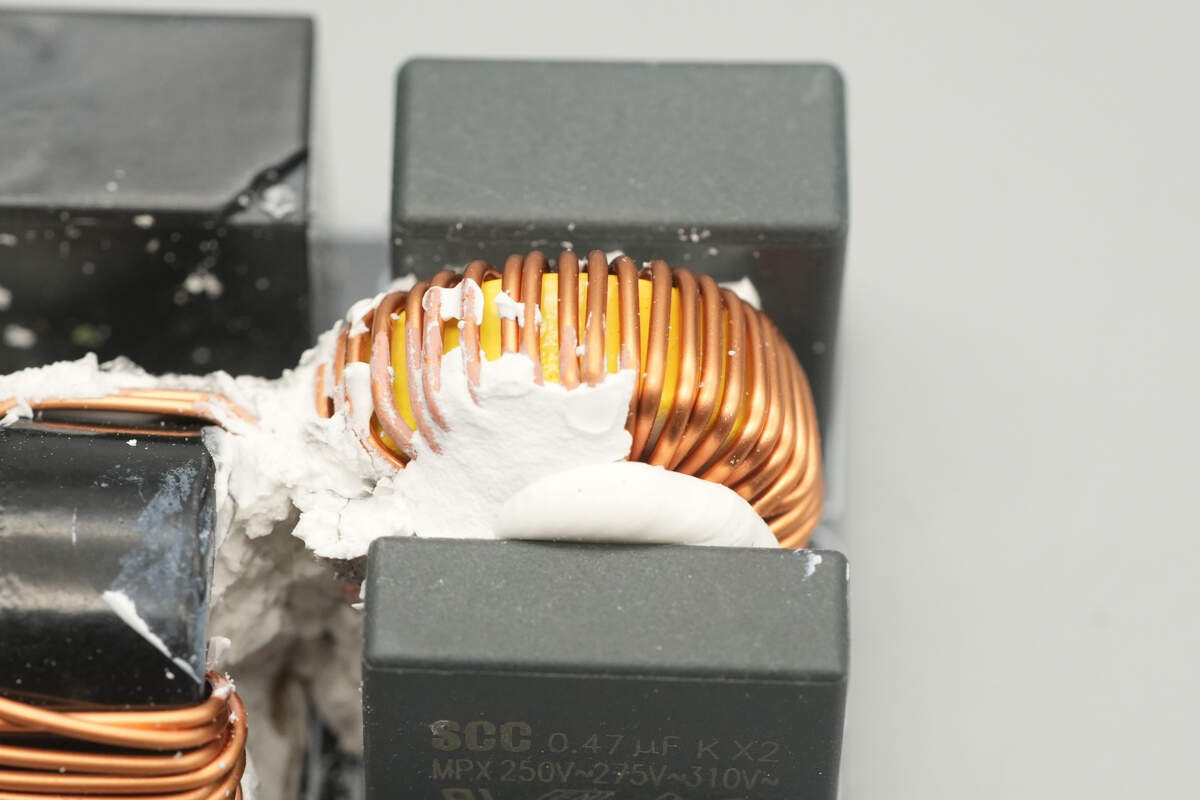
The filter inductor is wound on a ferrite core.
The safety X2 capacitor has a specification of 1 μF.
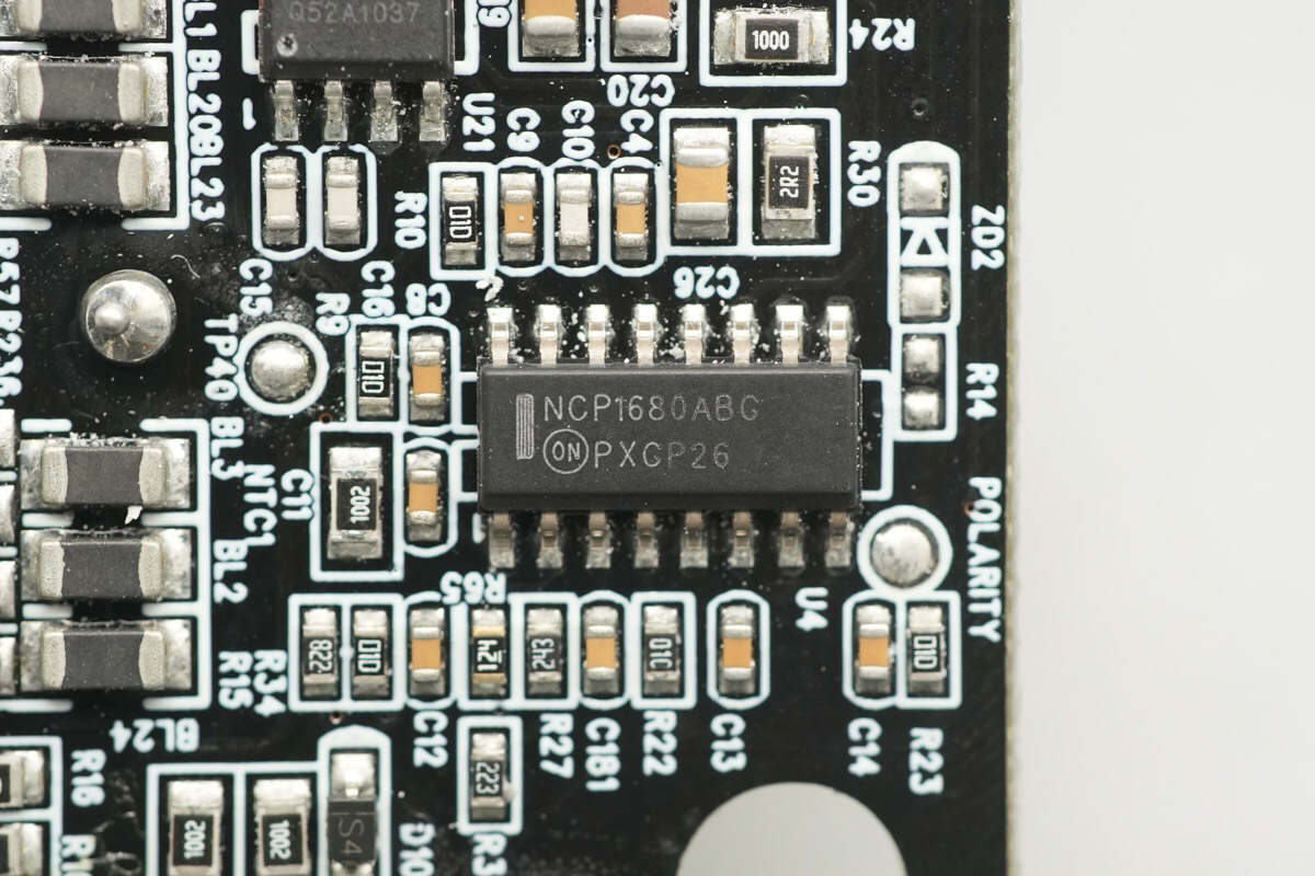
The totem-pole PFC controller is from Onsemi, model NCP1680. It integrates two half-bridges: one operates at the PWM switching frequency for PFC boost conversion, while the other functions at the AC line frequency for synchronous rectification. This design eliminates the losses associated with a traditional bridge rectifier, improving conversion efficiency and reducing thermal requirements. The controller is packaged in a SOIC-16.
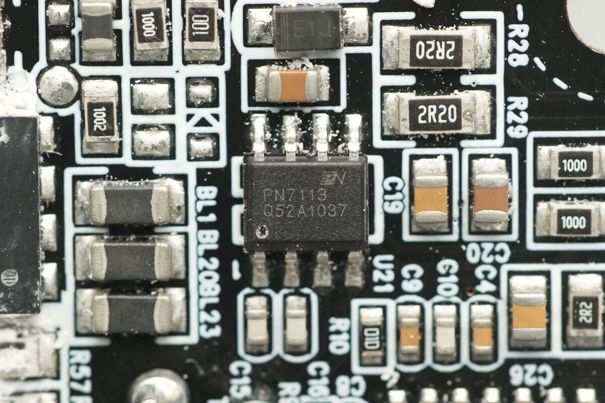
The driver is from Chipown, model PN7113. It is a half-bridge driver with a voltage rating of 600V and a driving capability of 2.5A, packaged in SOIC-8.
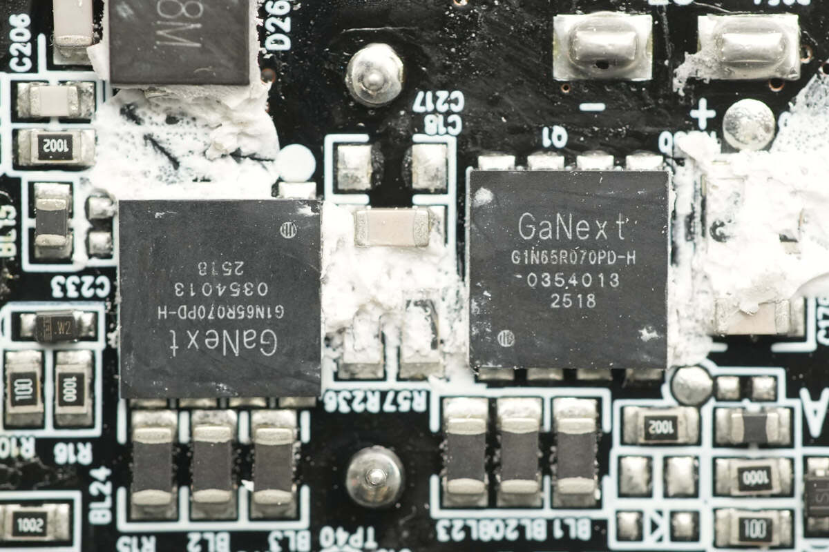
The PFC MOSFET is from GaNext, model G1N65R070PD-H. It is a 650V-rated gallium nitride (GaN) power device with a transient voltage tolerance of 800V. It features a typical Rds(on) of 70 mΩ and supports a gate voltage of ±20V, allowing it to be driven by conventional silicon MOSFET drivers. Compared to enhancement-mode GaN devices, it significantly simplifies gate drive circuit design. The device is packaged in XDFN8x8-8L, with the thermal pad connected to the source, which helps minimize high-frequency layout area and improve EMI performance.
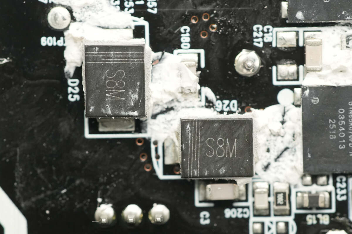
Two rectifiers are marked with S8M.
Close-up of the PFC boost inductor.
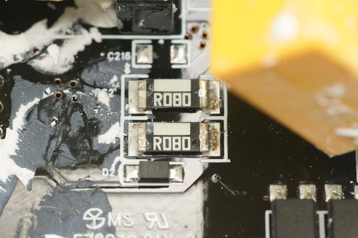
Two 80 mΩ resistors are connected in parallel for current sensing.
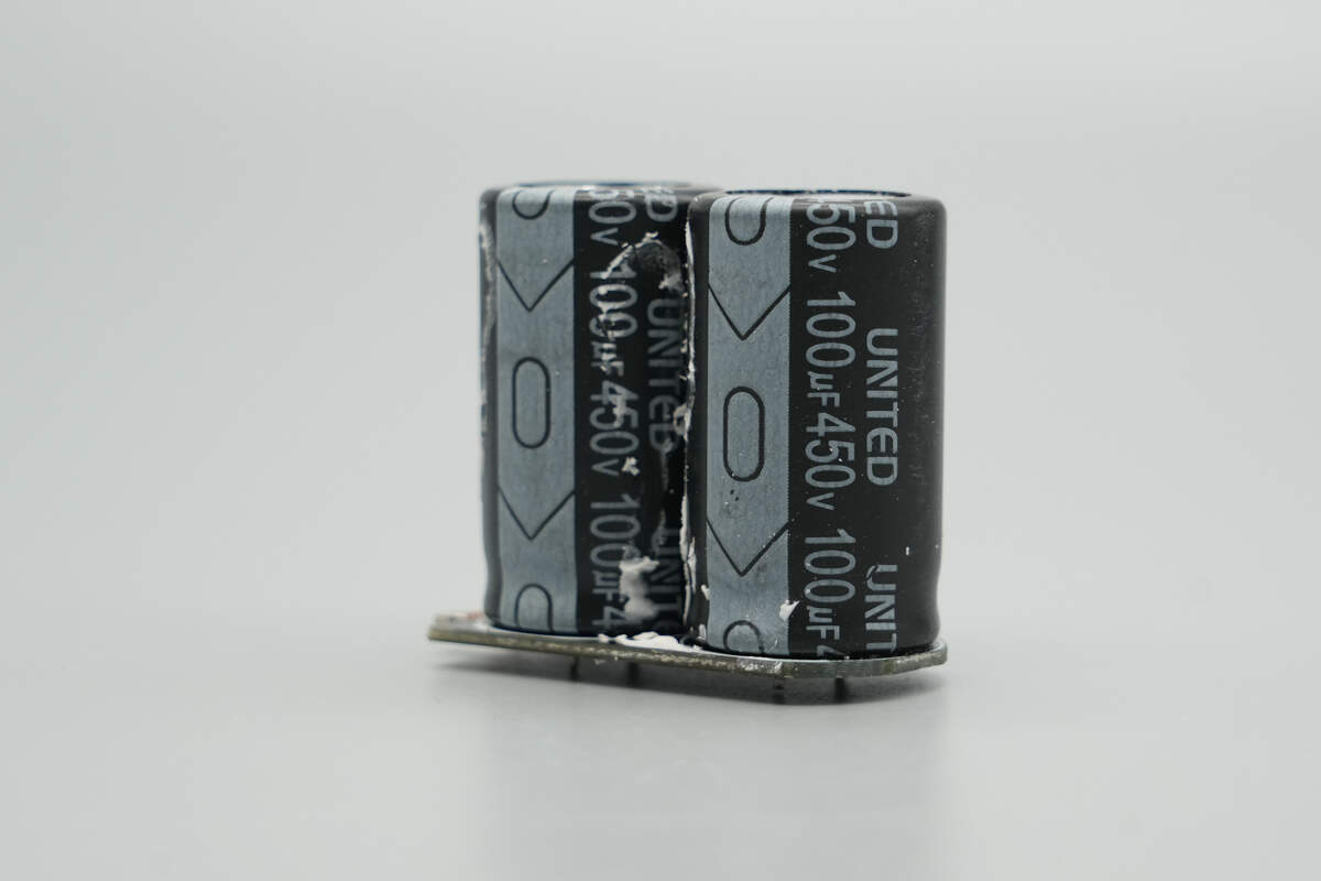
The filter capacitors are soldered onto a vertical PCB. They are supplied by UNITED, with a specification of 100 μF, 450 V.
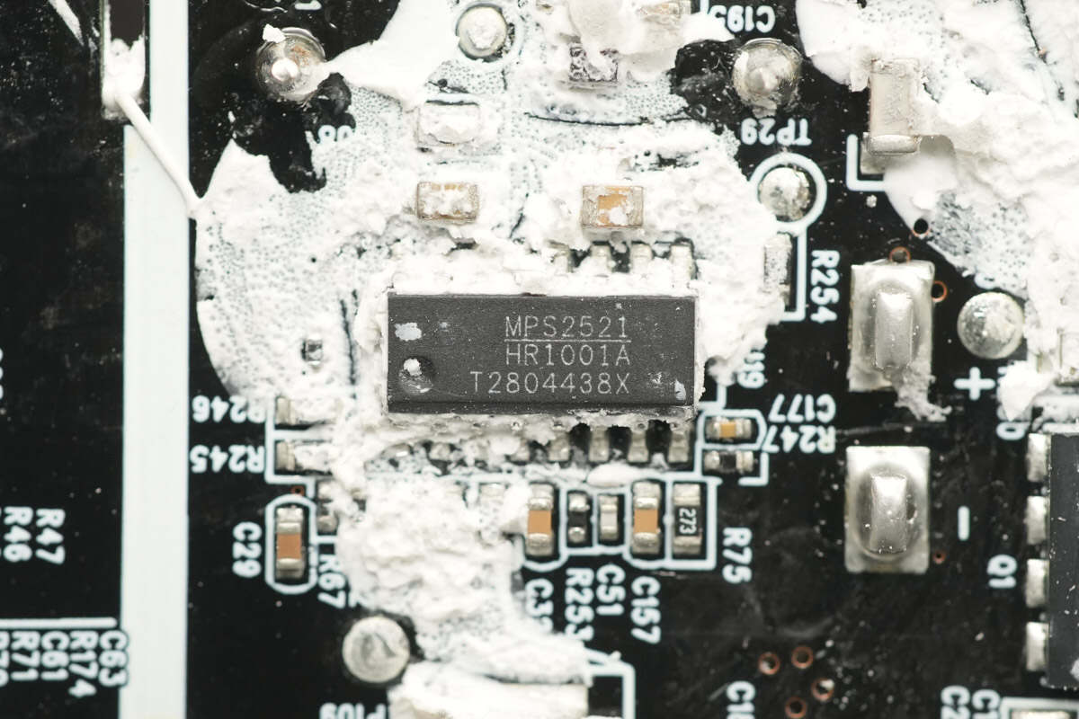
The LLC controller is from MPS, model HR1001A. It is an enhanced LLC controller featuring adaptive dead-time control and capacitive mode protection. The device offers dual-stage overcurrent protection, integrates an internal bootstrap diode, and supports remote on/off control and disable functions. It is packaged in SOIC-16.
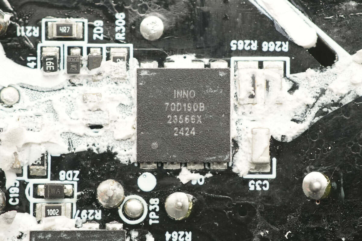
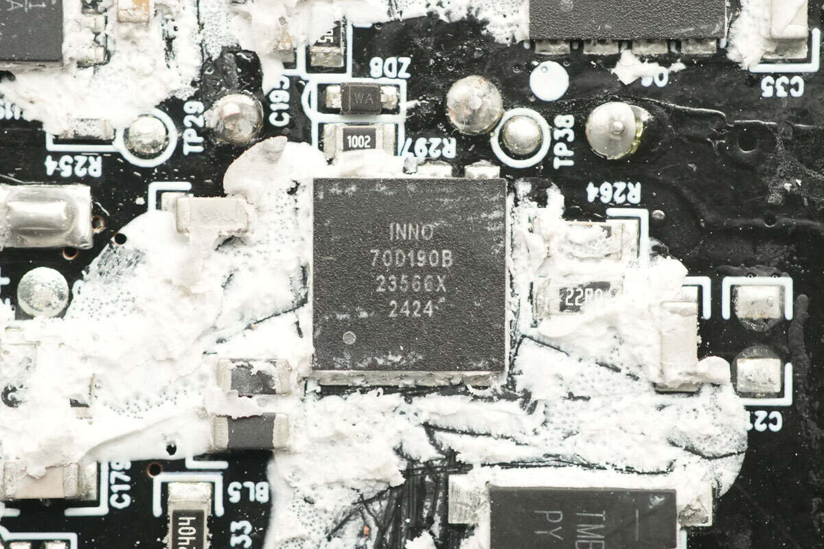
The LLC MOSFET is from Innoscience, model INN700D190B. It is a 700V-rated enhancement-mode GaN transistor, upgraded from the previous 650V rating, with a transient voltage tolerance of 800V. The device features an Rds(on) of 190mΩ, supporting higher power applications.
It supports ultra-high switching frequencies with no reverse recovery charge and has very low gate and output charge. The device meets JEDEC standards for industrial applications, includes built-in ESD protection, and complies with RoHS, lead-free, and EU REACH regulations. It is suitable for high-efficiency, high-density applications such as AC-DC and DC-DC conversion. The package type is DFN 8x8.
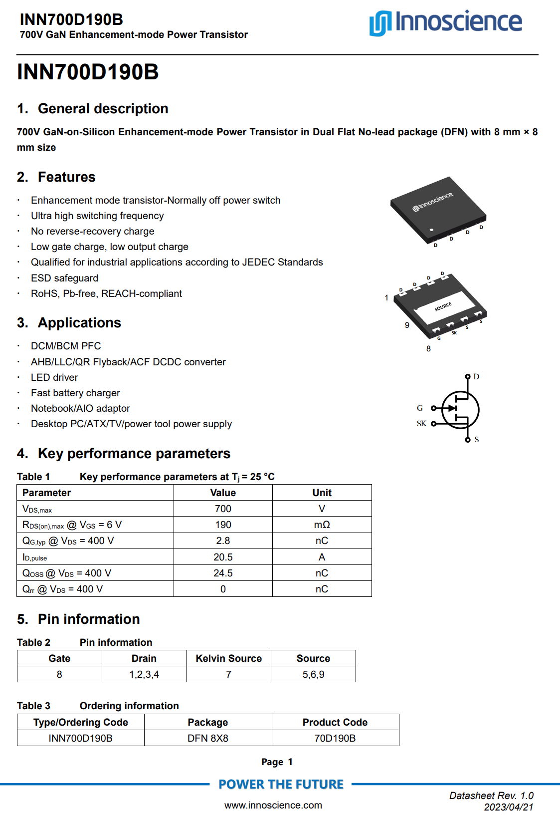
Here is the information about Innoscience INN700D190B.
The other LLC MOSFET has the same model.
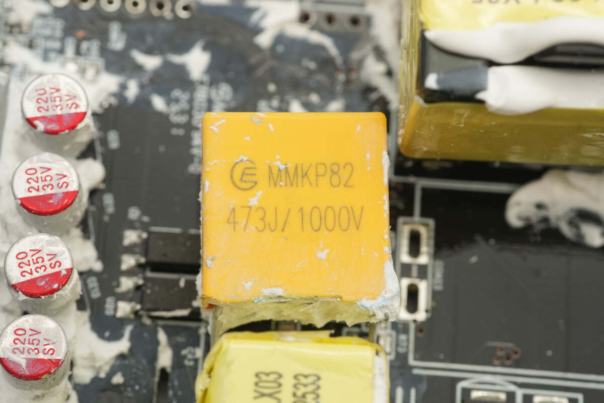
The resonant capacitor is specified at 0.047 μF, 1000 V.

The resonant inductor is tightly wrapped with insulating tape.
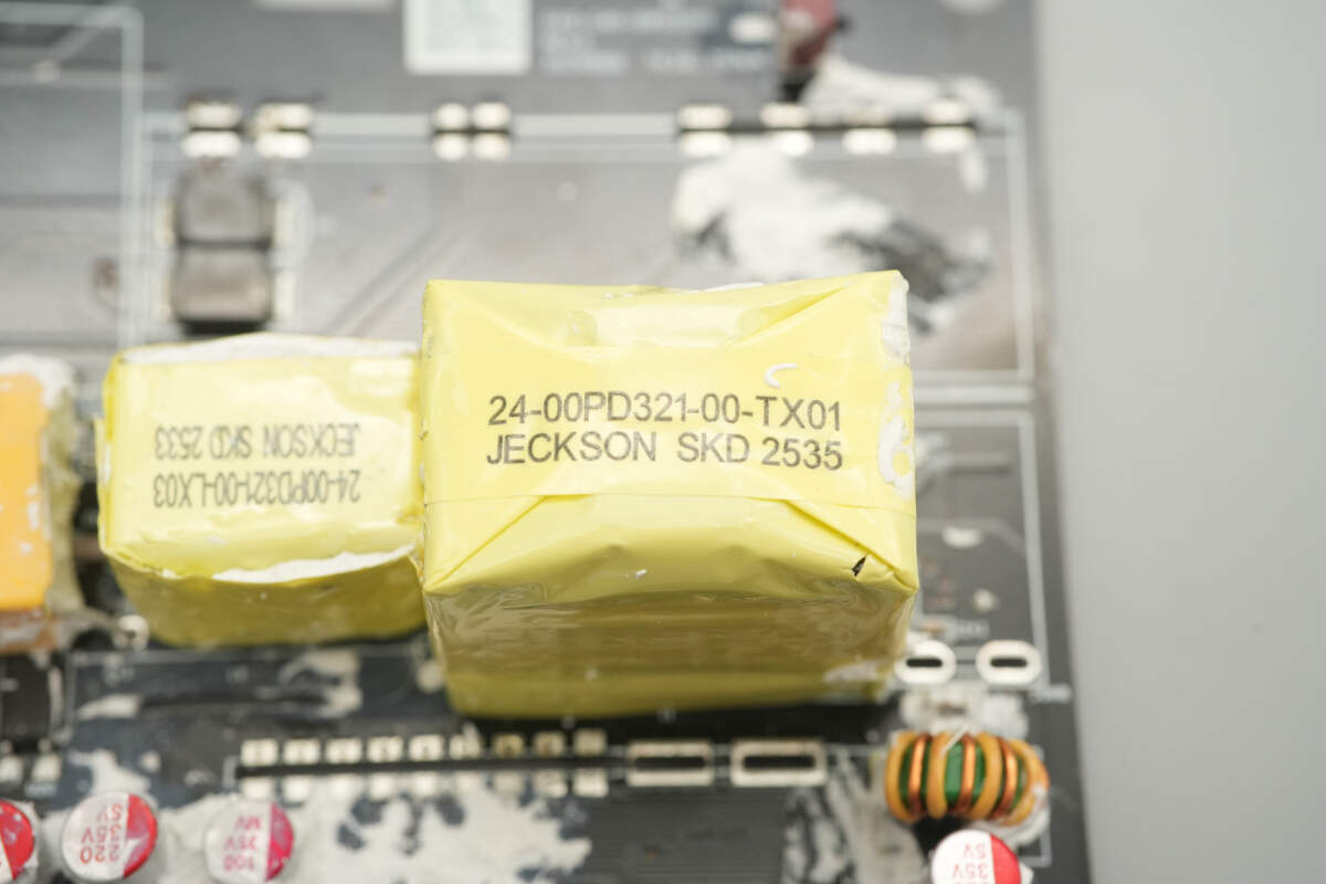
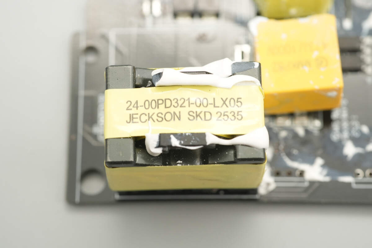
The LLC transformer is also tightly wrapped with insulating tape.
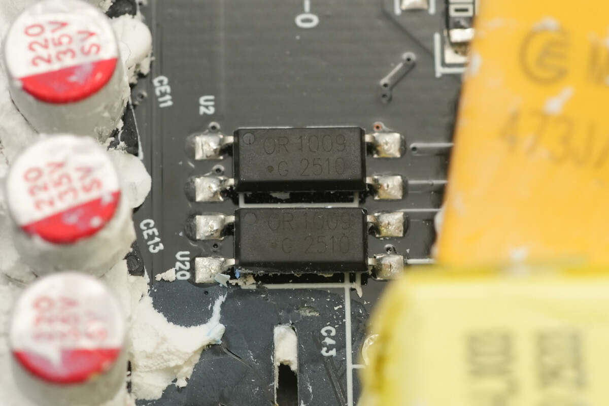
The OR OR-1009 optocouplers are used for output voltage feedback and output overvoltage protection functions.
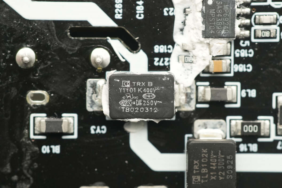
The SMD Y capacitor is from TRX. Its compact size and lightweight design make it ideal for high-density power products such as GaN fast chargers. The part number is TMY1101K.

The synchronous rectifier controller is from MPS, model MP6924B. It is an LLC synchronous rectifier controller featuring enhanced interference immunity and fast shutdown capability, compatible with CCM and DCM modes. The chip integrates two synchronous rectifier controllers internally, each dedicated to rectification of the two LLC secondary coil outputs. It is designed for LLC converter synchronous rectification applications and is packaged in SOIC-8.
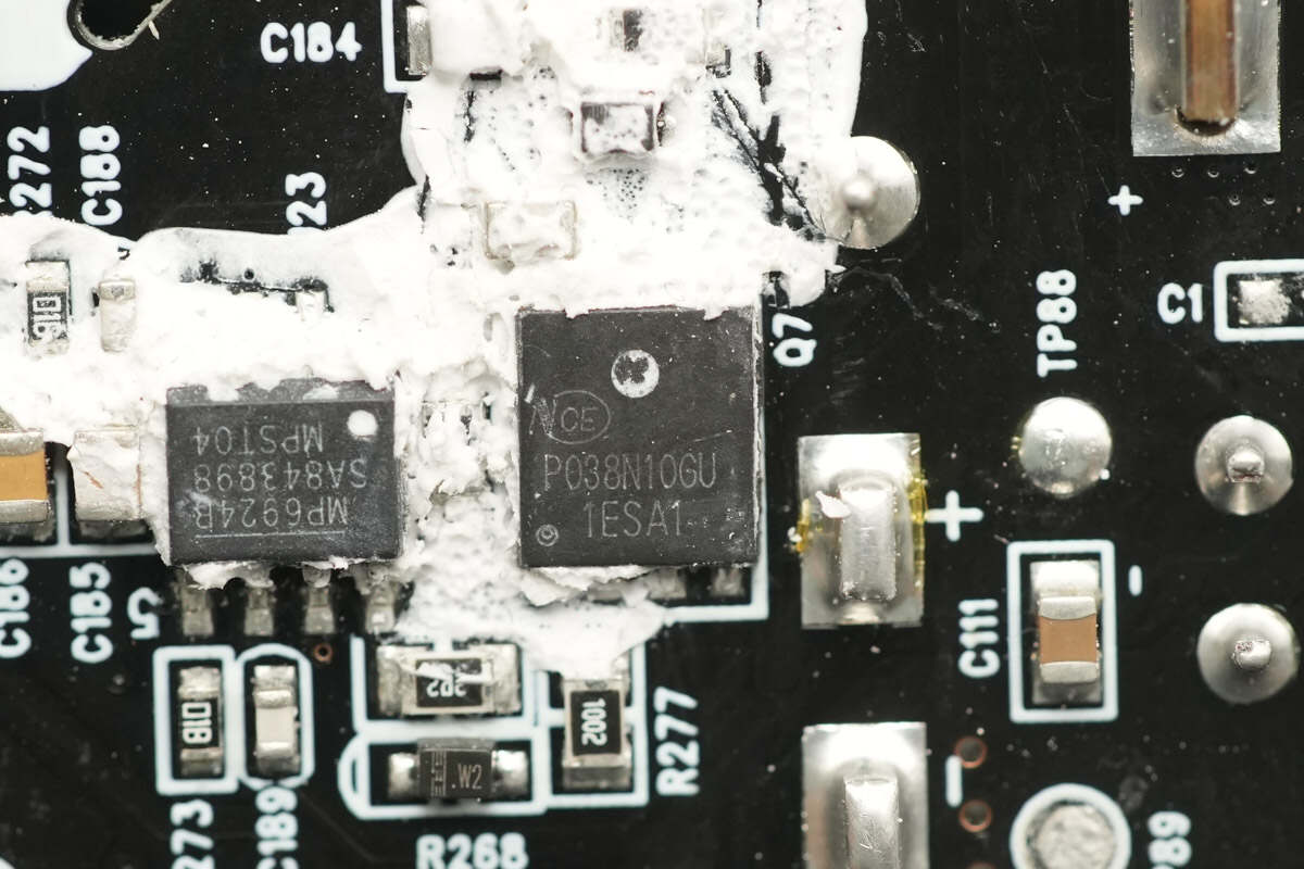
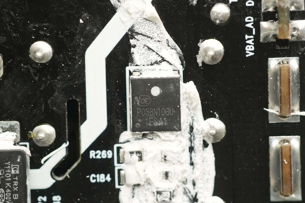
The synchronous rectifier is from NCE, model NCEP038N10GU. It is an NMOS device with a voltage rating of 100V and an Rds(on) of 3.45 mΩ, packaged in DFN 5×6.
The other synchronous rectifier has the same model.

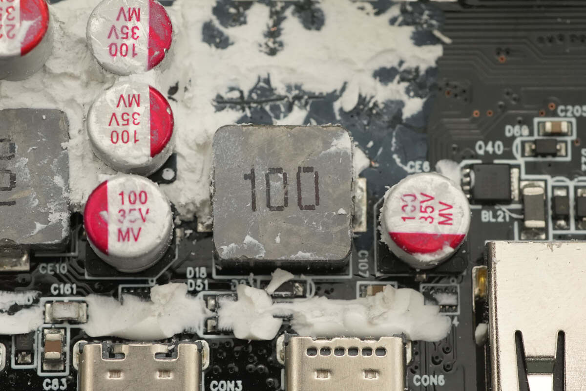
The output filter capacitors are from Relon, H2 series solid electrolyte aluminum electrolytic capacitors, each rated at 1000 μF, 35 V, connected in parallel with three units.
The filter inductor is wound with insulated wire and enameled wire.
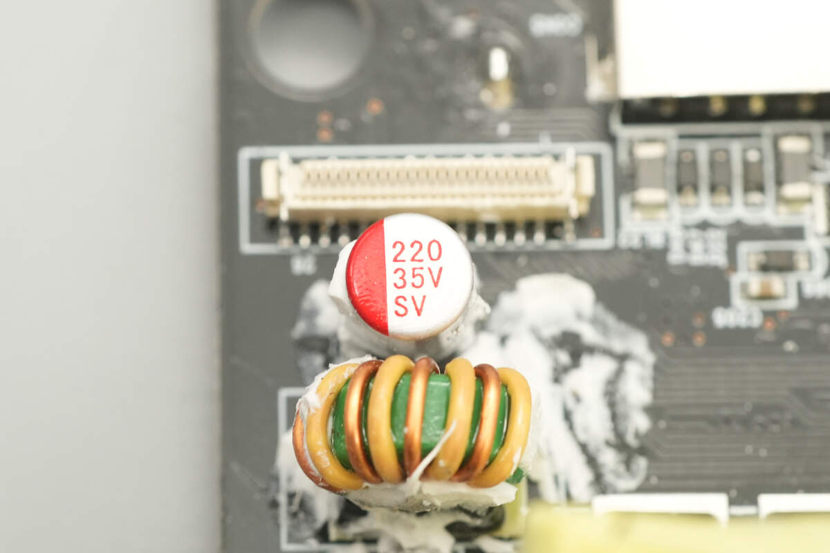
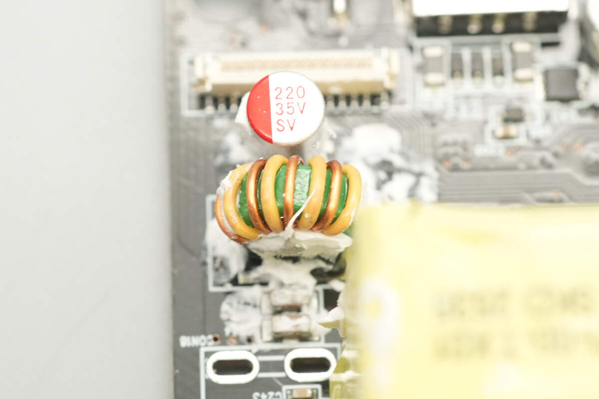
The filter capacitor has a specification of 220 μF, 35 V.
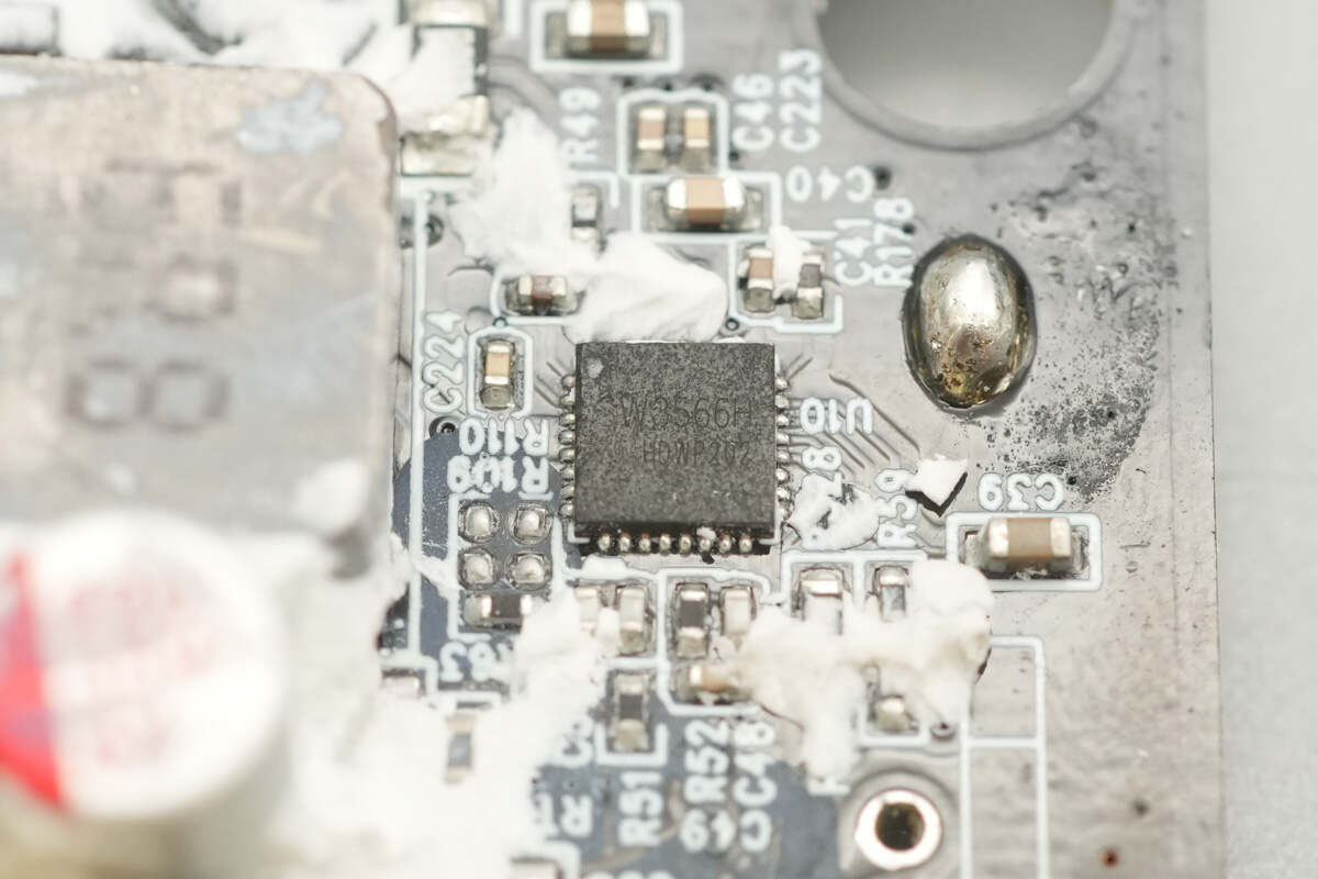
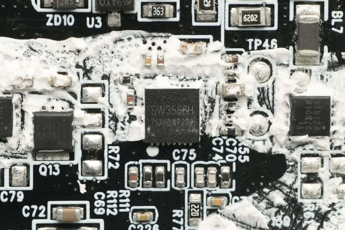
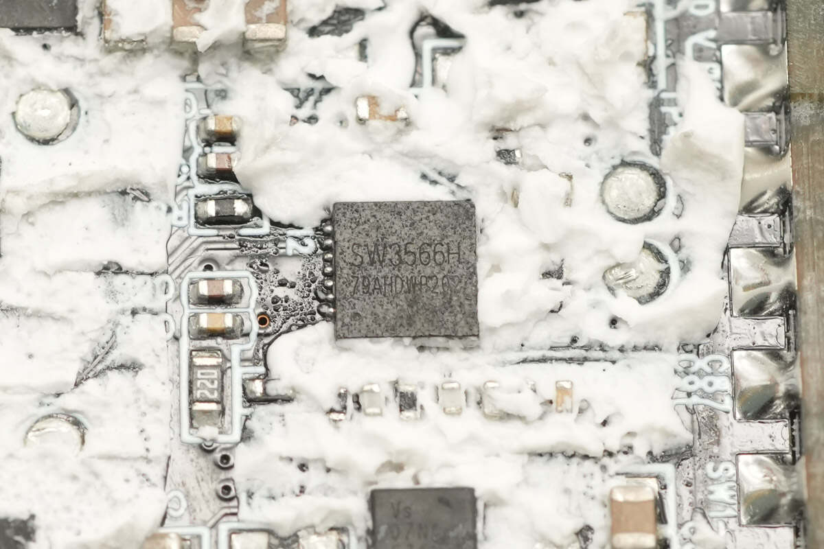
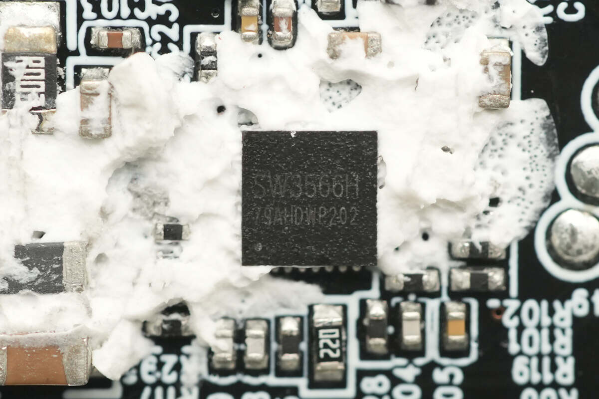
The buck protocol chip for USB-C1 is from iSmartWare, model SW3566H. It is a highly integrated dual-port fast charging SoC that supports both USB-C and USB-A interfaces with independent current limiting for each port. The chip integrates a high-efficiency synchronous buck converter and supports output up to 20 V/7 A and 28 V/5 A, with compatibility for fast charging protocols including PD3.1, QC, SCP, and UFCS. Custom protocol configurations are also supported, with a maximum output power of 140 W.
The device includes CC/CV modes, dual-port management logic, and bus voltage detection. With appropriate buck and VBUS MOSFETs, it enables dual-port buck output. The built-in buck converter operates at 180 kHz and supports both PWM and PFM modes. Protection thresholds for output current, line loss compensation, and more can be configured via an I²C interface. An integrated ADC supports data sampling across nine channels, including input/output voltage, output current, and chip temperature, and it supports external MCU integration for parameter monitoring.
It supports up to 36 V input voltage and a maximum output current of 7 A. The chip includes built-in soft start, input overvoltage/undervoltage protection, output overvoltage/undervoltage protection, output overcurrent/short-circuit protection, DP/DM/CC overvoltage protection, thermal protection, external NTC thermistor protection, and power limiting. It is packaged in a QFN 4×4–32.
Here is the information about iSmartWare SW3566.
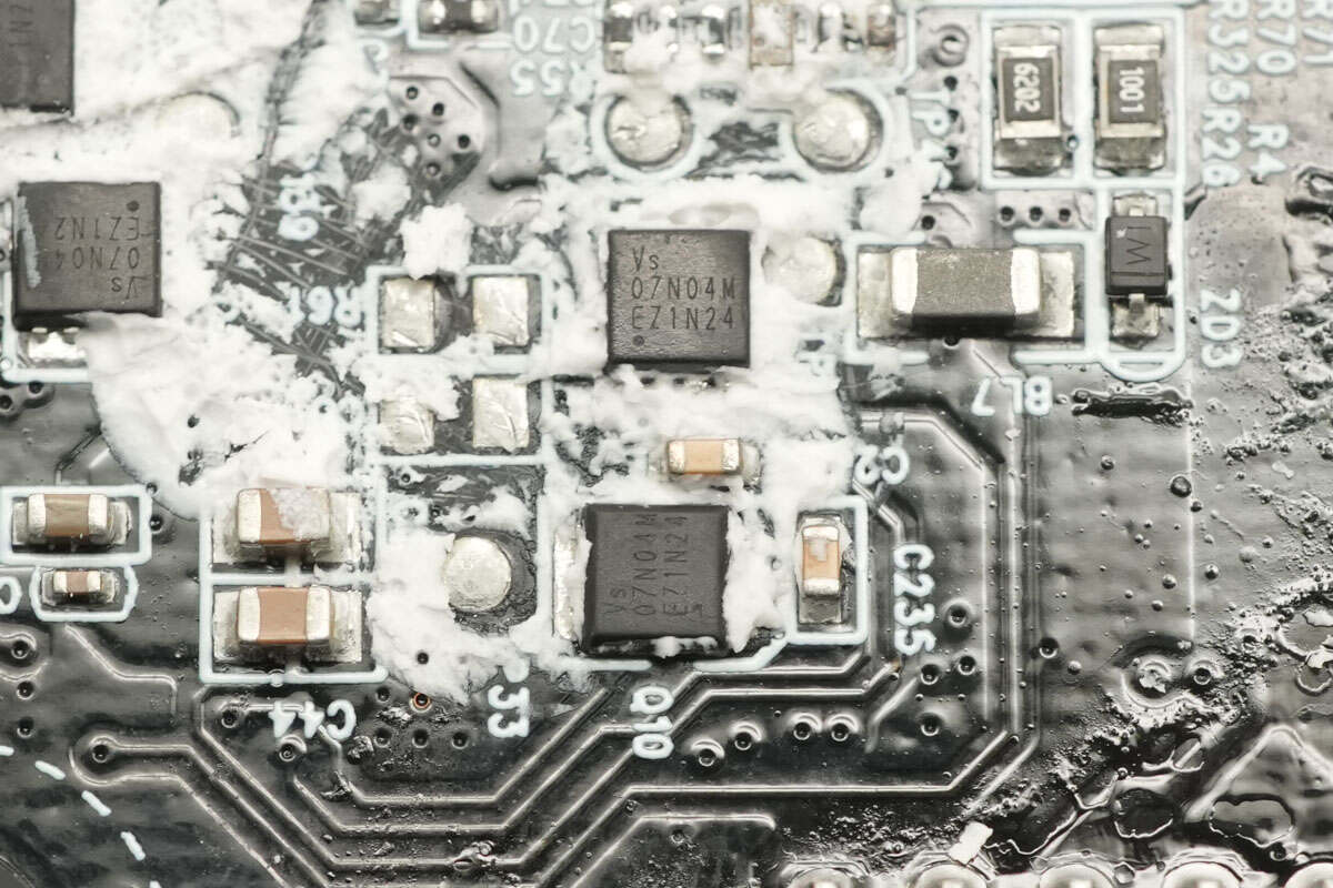
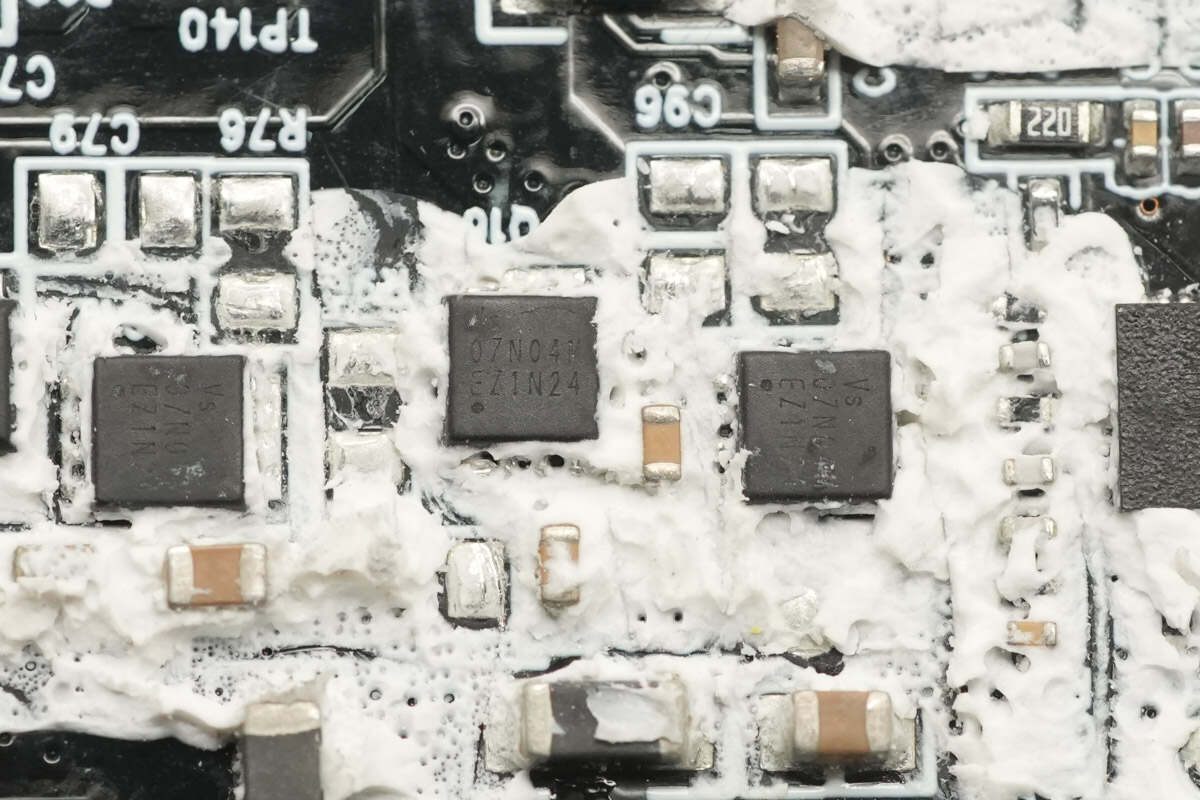
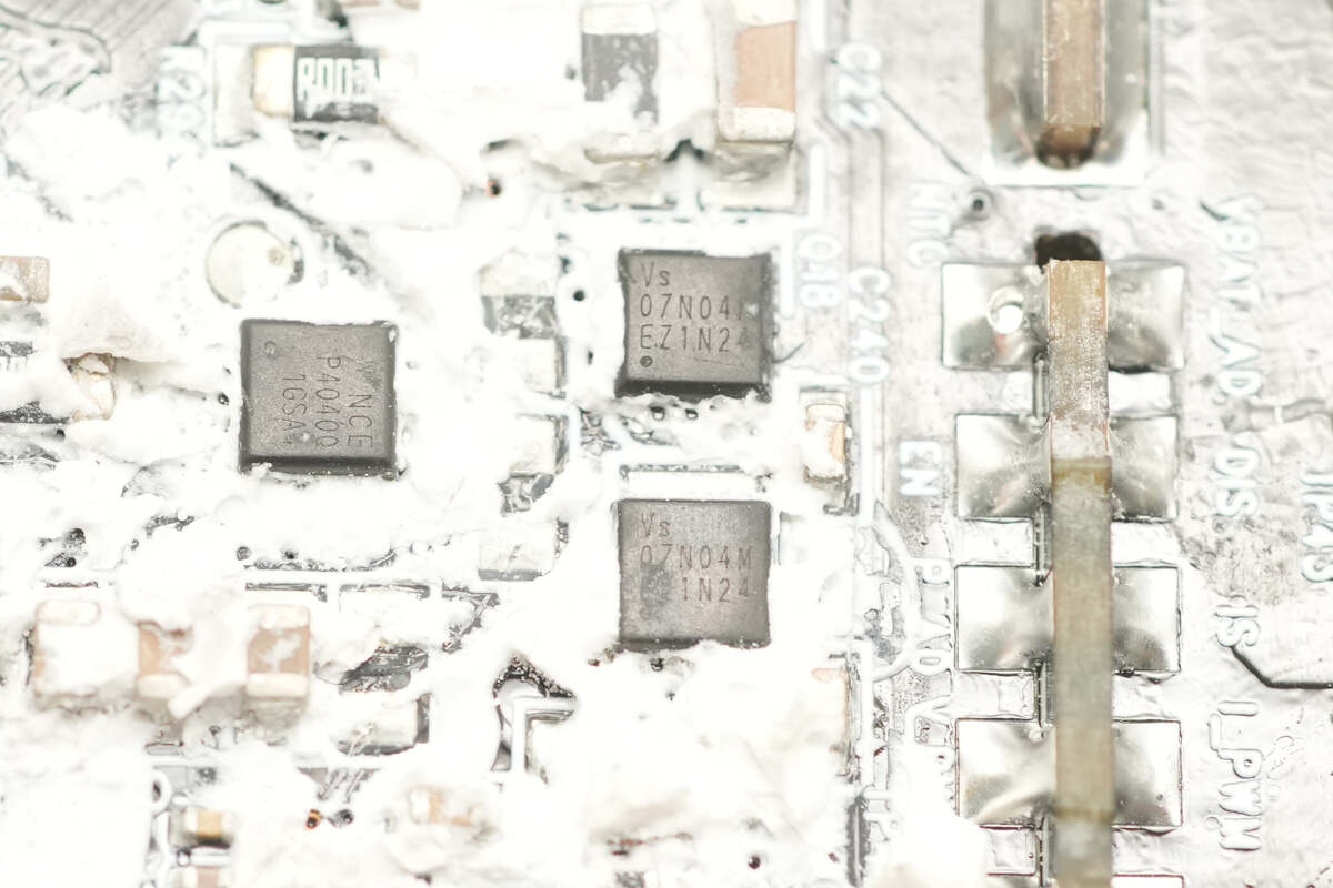
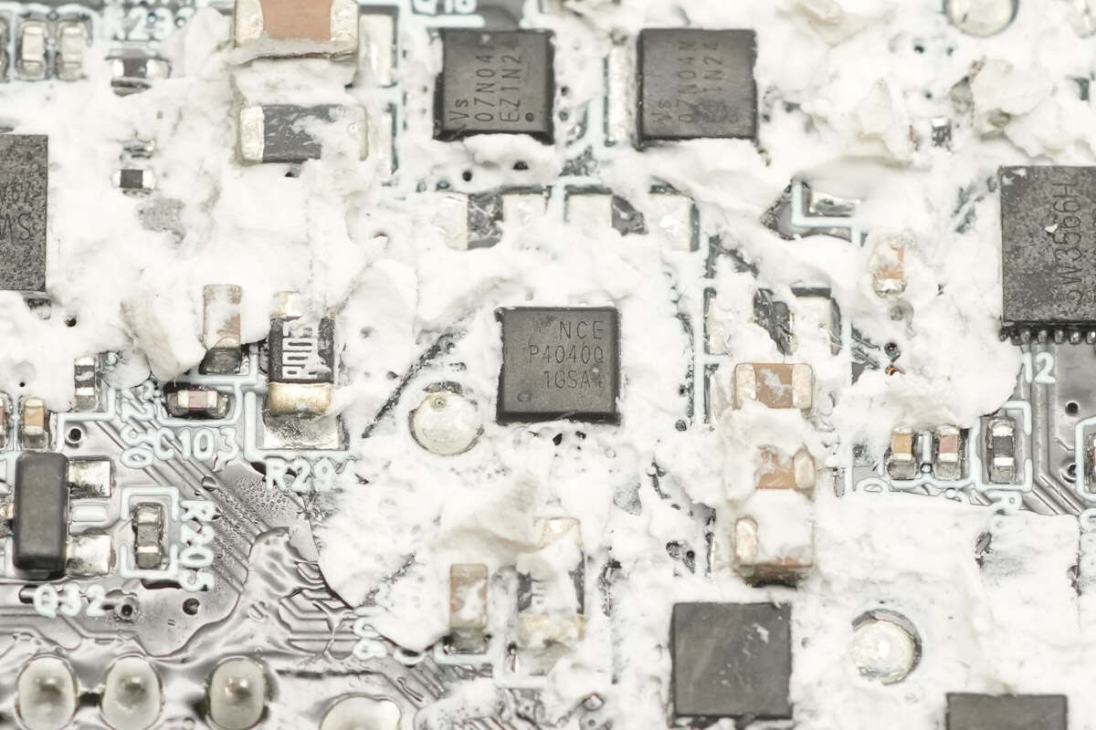
The synchronous buck MOSFETs are from Vergiga, marked with 07N04M, model VSE007N04MS-G. They are NMOS devices rated at 40V with an Rds(on) of 3.2 mΩ, packaged in PDFN 3×3×3.

Here is the information about Vergiga VSE007N04MS-G.
The VBUS MOSFETs also use the Vergiga VSE007N04MS-G.
The USB-C2 port uses the iSmartWare SW3566H buck protocol chip.
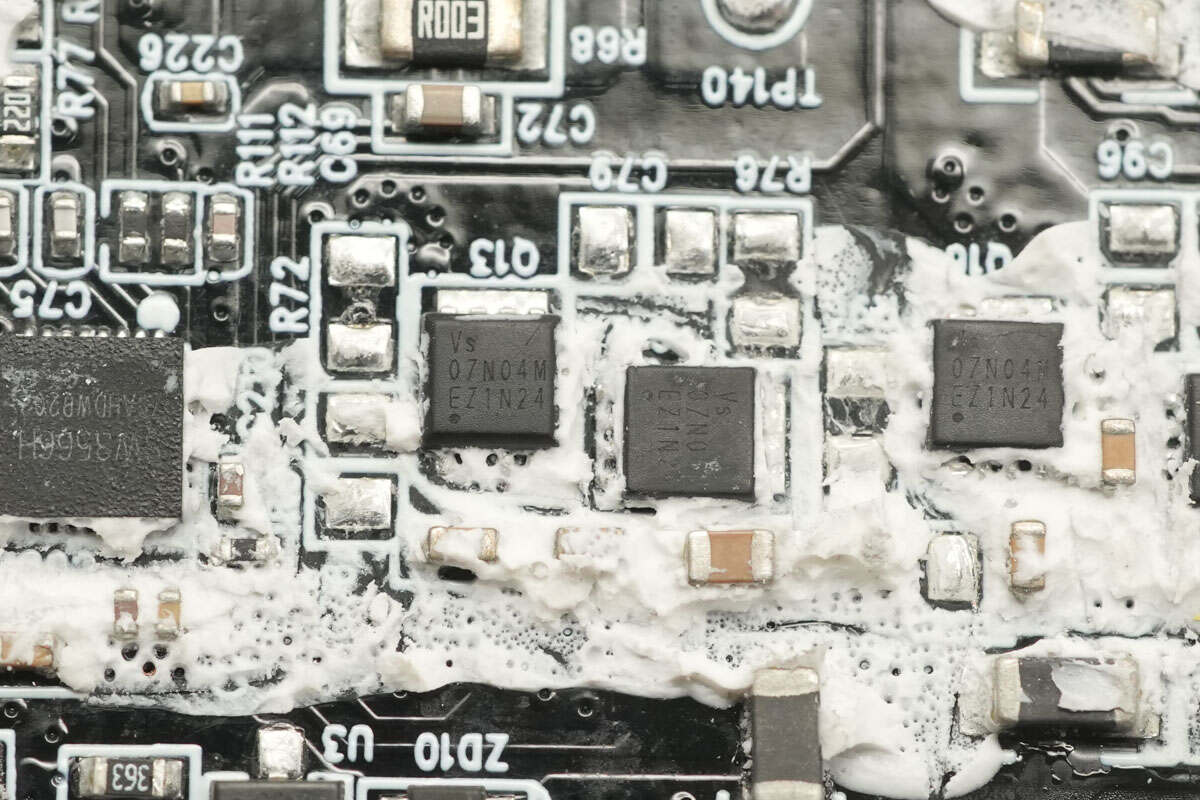
The synchronous buck MOSFETs also use Vergiga VSE007N04MS-G.
The VBUS MOSFETs also use Vergiga VSE007N04MS-G.
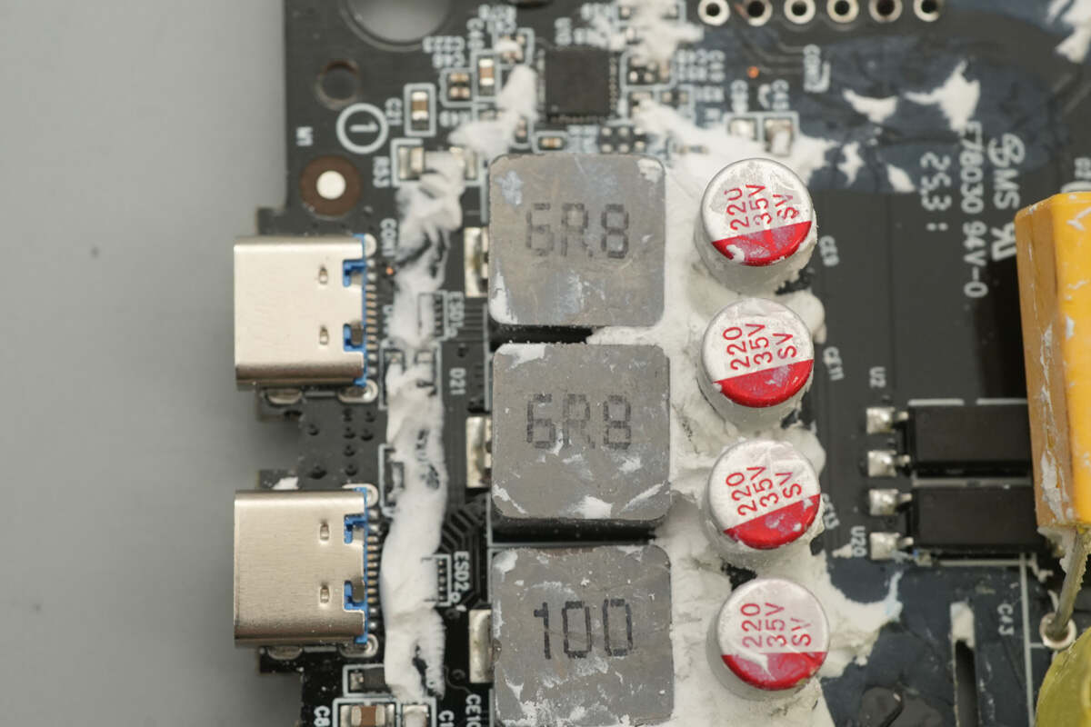
The buck inductors for both USB-C1 and USB-C2 ports are rated at 6.8 μH.
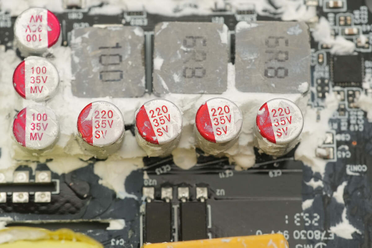
The filter capacitors have a specification of 220 μF, 35 V.
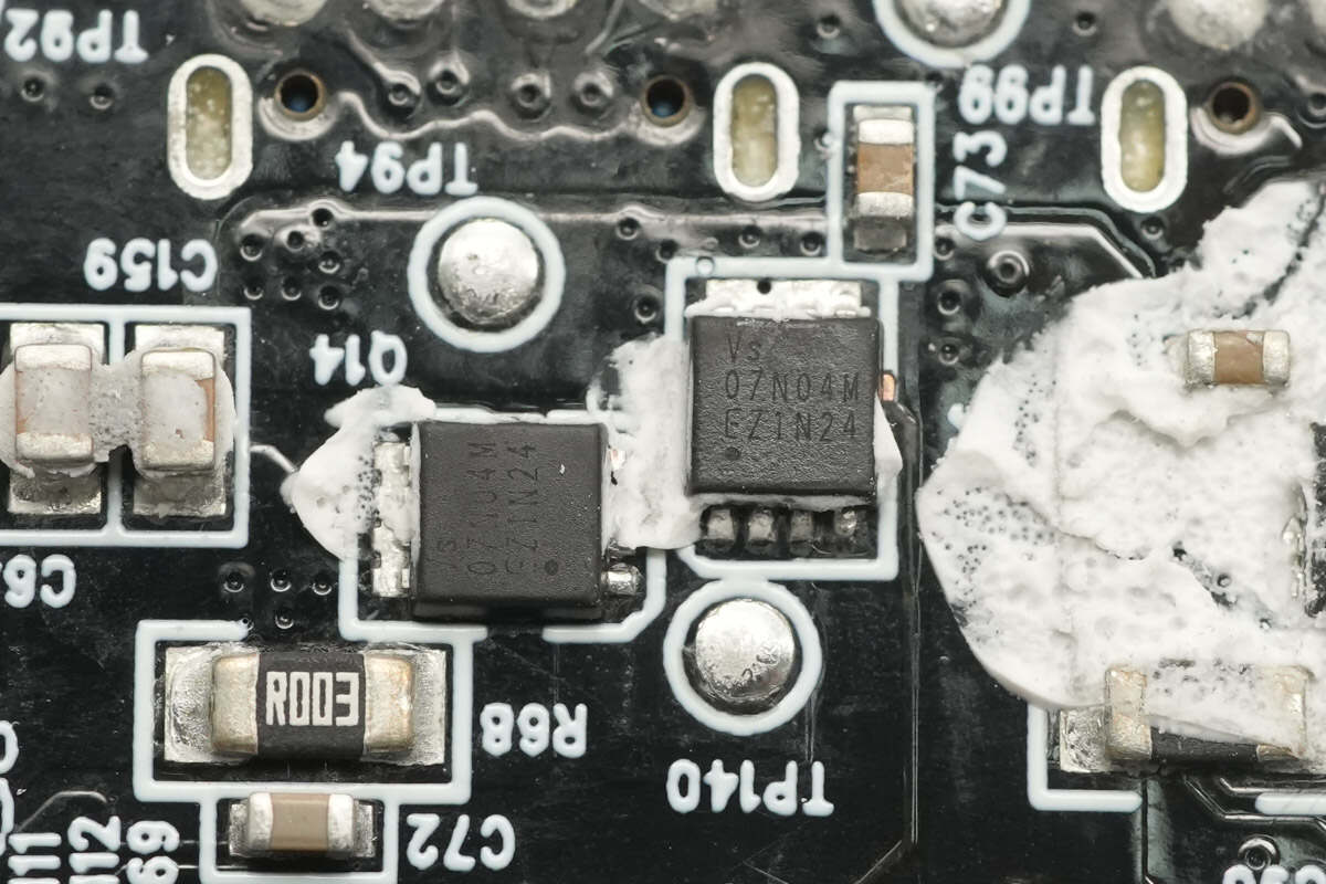
The USB-C3 port uses the iSmartWare SW3566H buck protocol chip.
The synchronous buck MOSFETs also use Vergiga VSE007N04MS-G.
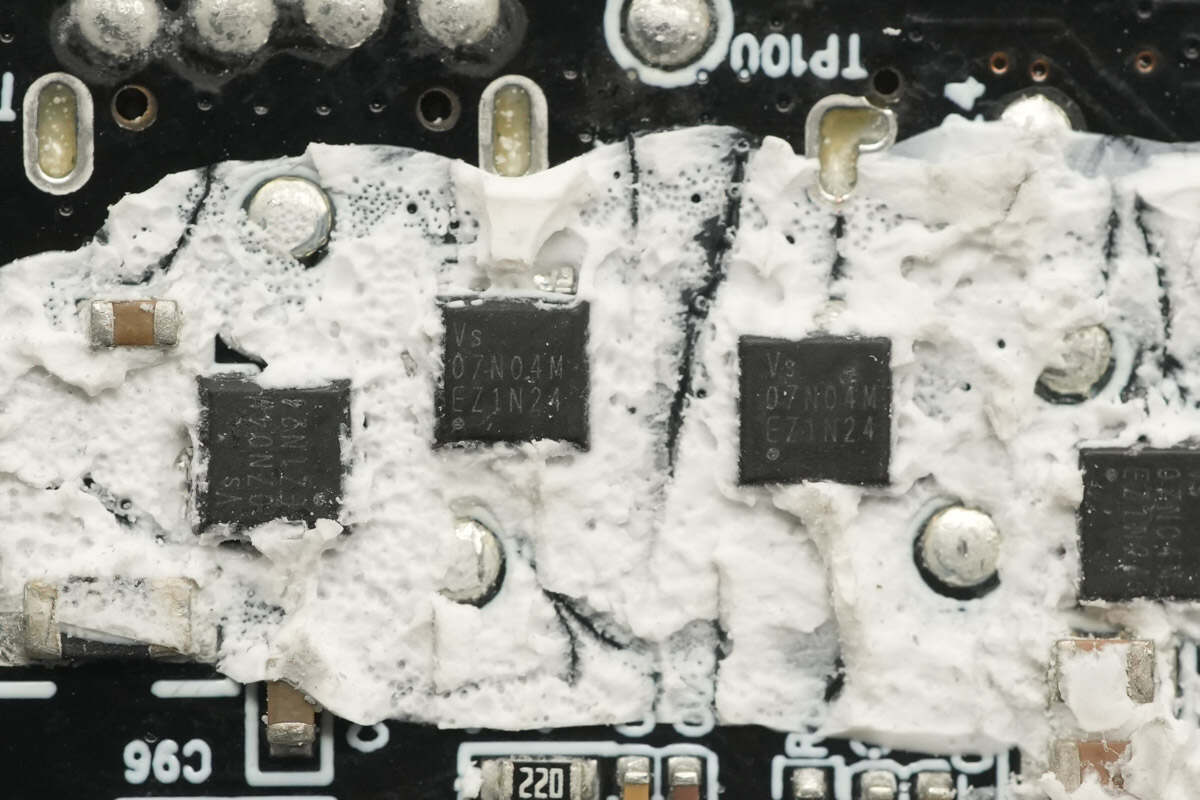
The VBUS MOSFETs also use Vergiga VSE007N04MS-G.
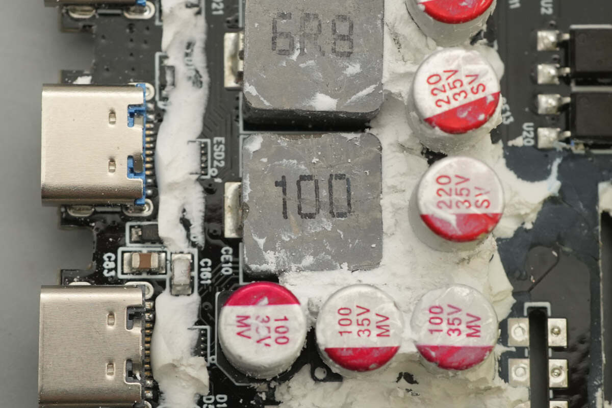
The USB-C3 port uses a 10 μH buck inductor.
The USB-C4 and USB-A ports use the iSmartWare SW3566H buck protocol chip.
The synchronous buck MOSFETs also use Vergiga VSE007N04MS-G.
The USB-A port VBUS MOSFET uses NCE NCEP4040Q. It is NMOS devices rated at 40V with an Rds(on) of 7.7 mΩ, packaged in DFN 3.3×3.3.
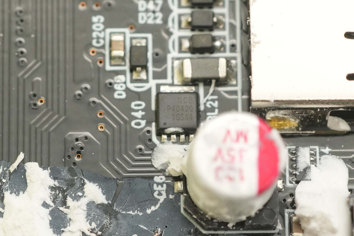
The other VBUS MOSFET has the same model.
The USB-C4 port uses a 10 μH buck inductor.
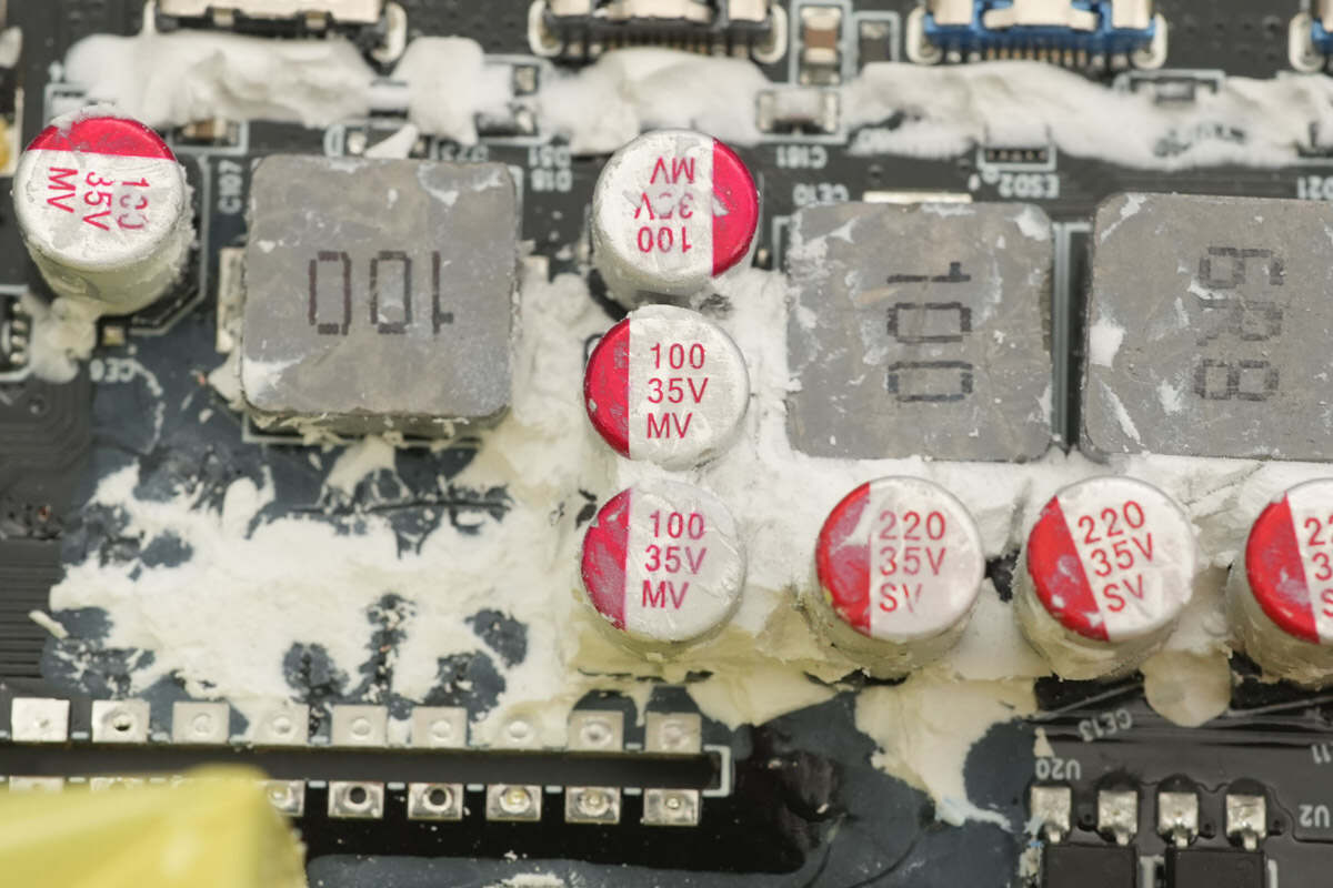
Three filter capacitors, each rated at 100 μF, 35 V.
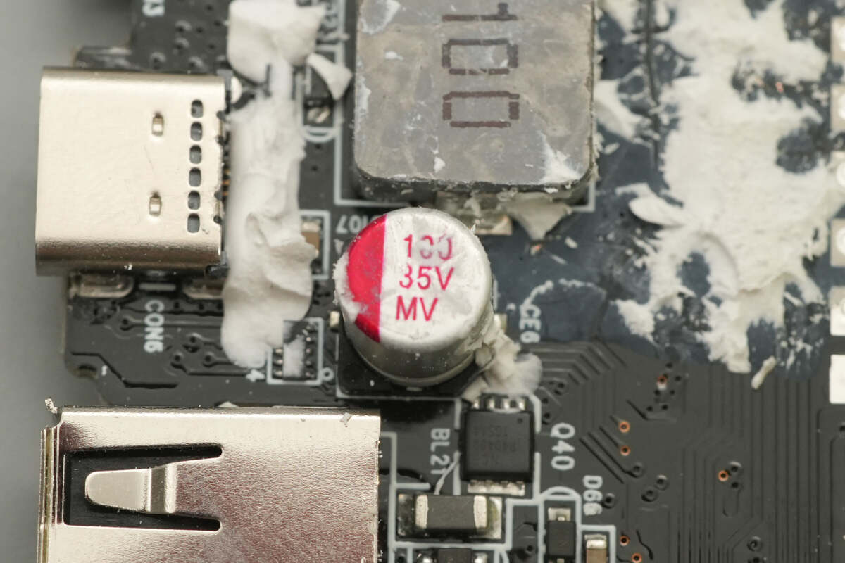
The filter capacitor has a specification of 100 μF, 35 V.
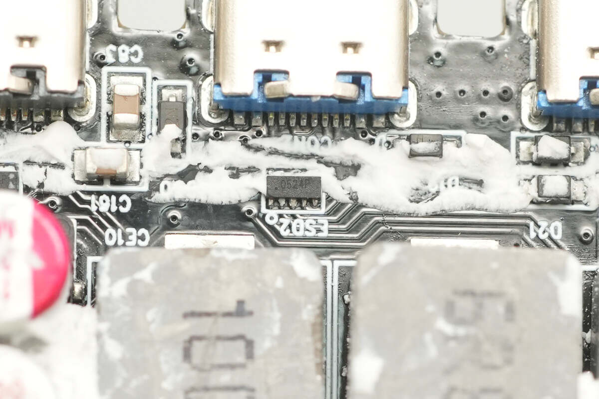
The TVS array marked with 0524P is used for electrostatic discharge protection.

The front side of the buck PCB features a fuse, a toroidal inductor, and filter capacitors.
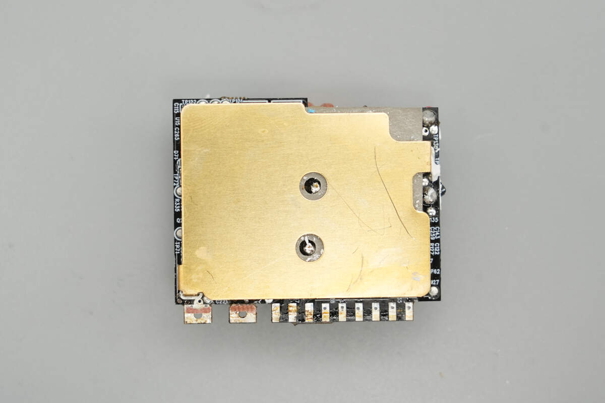
The back side of the PCB is equipped with a brass heat sink.

After removing the heat sink, the back side reveals thermal grease and a thermal pad.
The back side contains the synchronous buck controller, buck MOSFETs, an operational amplifier, current sensing resistors, and a sampling amplifier.
The synchronous buck controller is from JOULWATT, model JWH6344. It supports an input voltage range of 6–65 V and an output voltage range of 0.8–55 V. The controller operates at a switching frequency between 100 kHz and 1 MHz and features both synchronous signal input and output. It includes programmable current limiting and is packaged in QFN-20.

Here is the information about JOULWATT JWH6344.
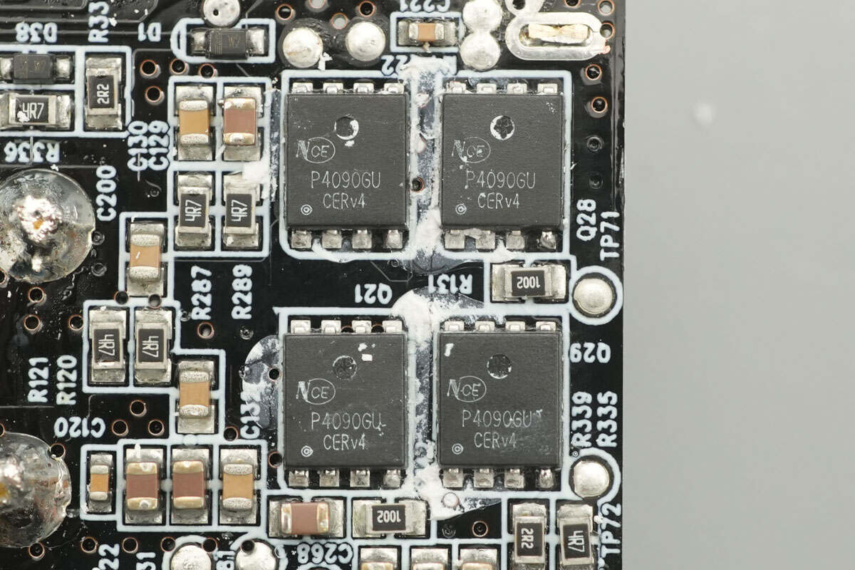
The synchronous buck MOSFETs are from NCE, model NCEP4090GU. They have a voltage rating of 40V and an Rds(on) of 2.2 mΩ, packaged in DFN 5×6.
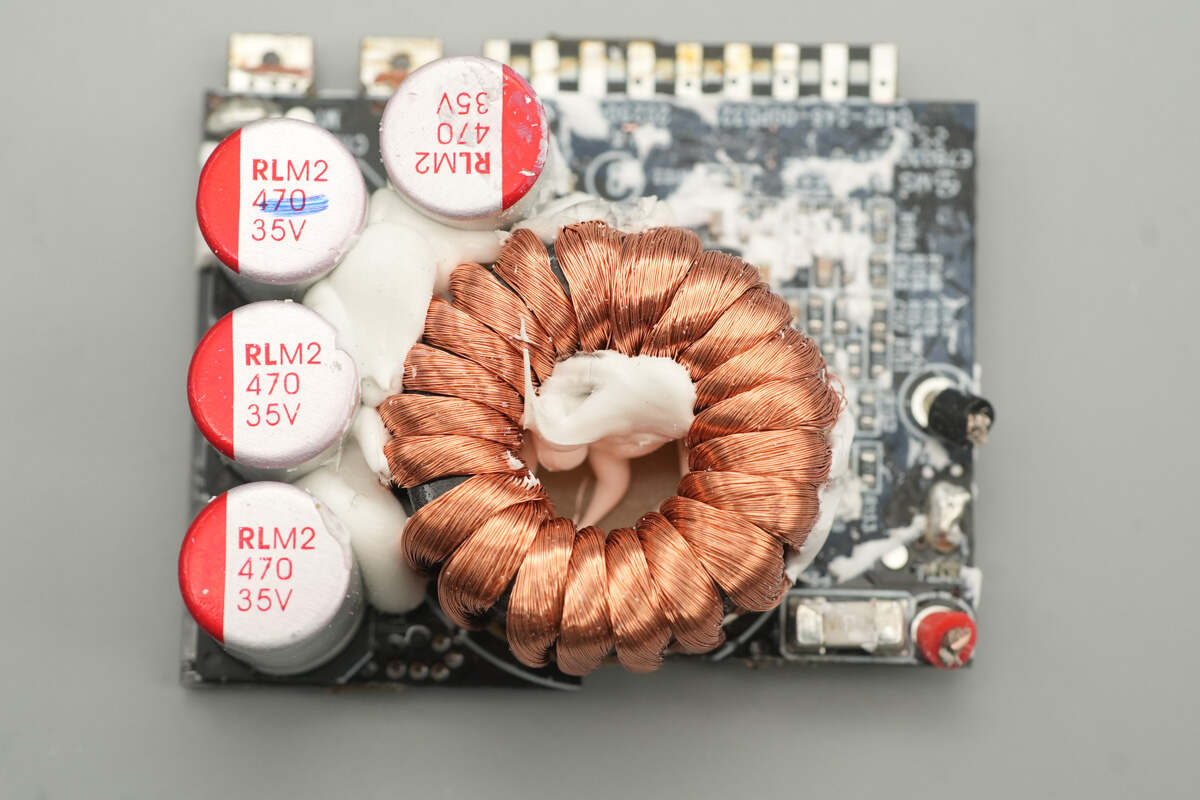
The buck inductor is wound with Litz wire.
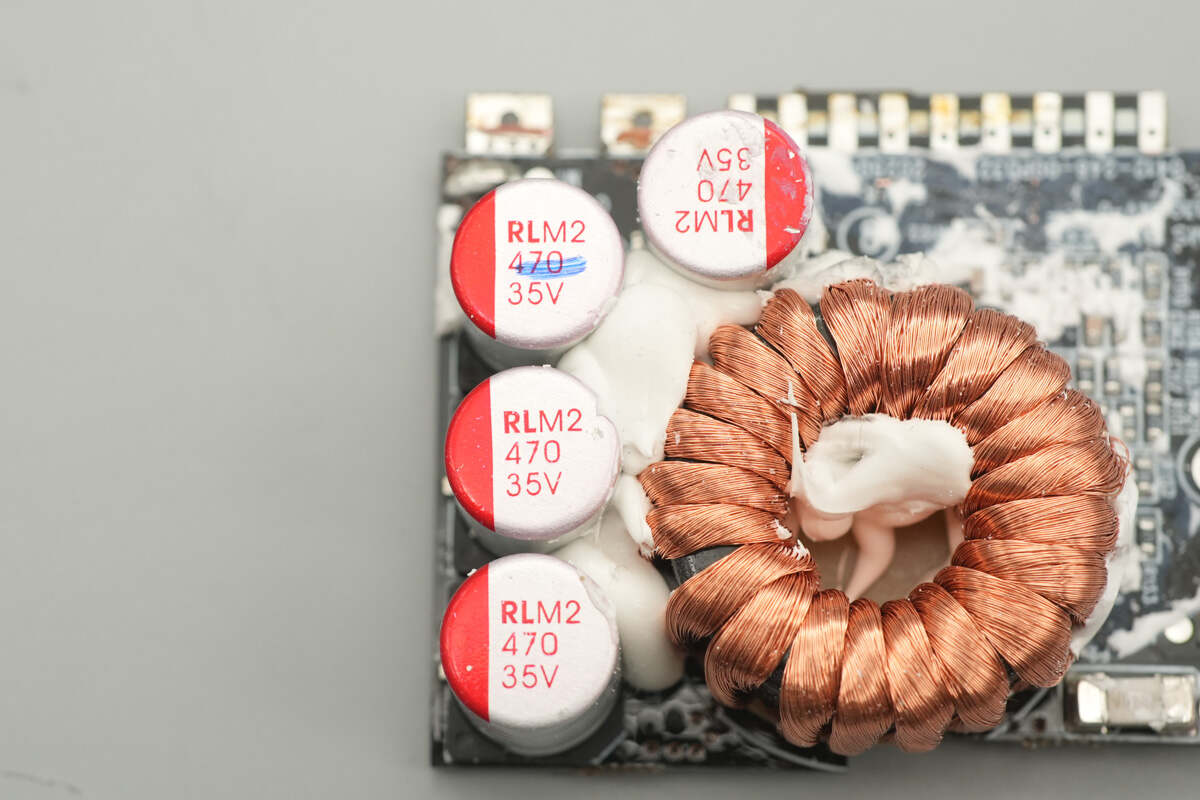
The filter capacitors are from Relon, with a specification of 470 μF, 35 V.
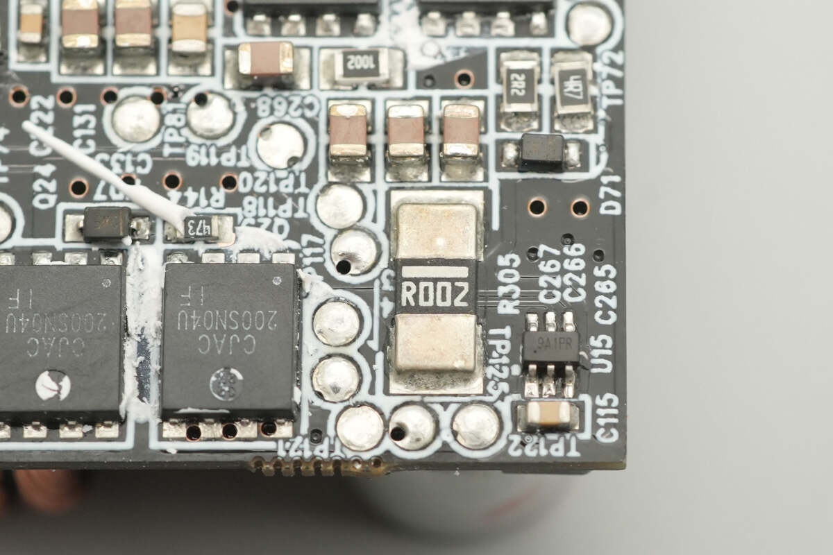
A 2 mΩ sensing resistor is used for output current detection.
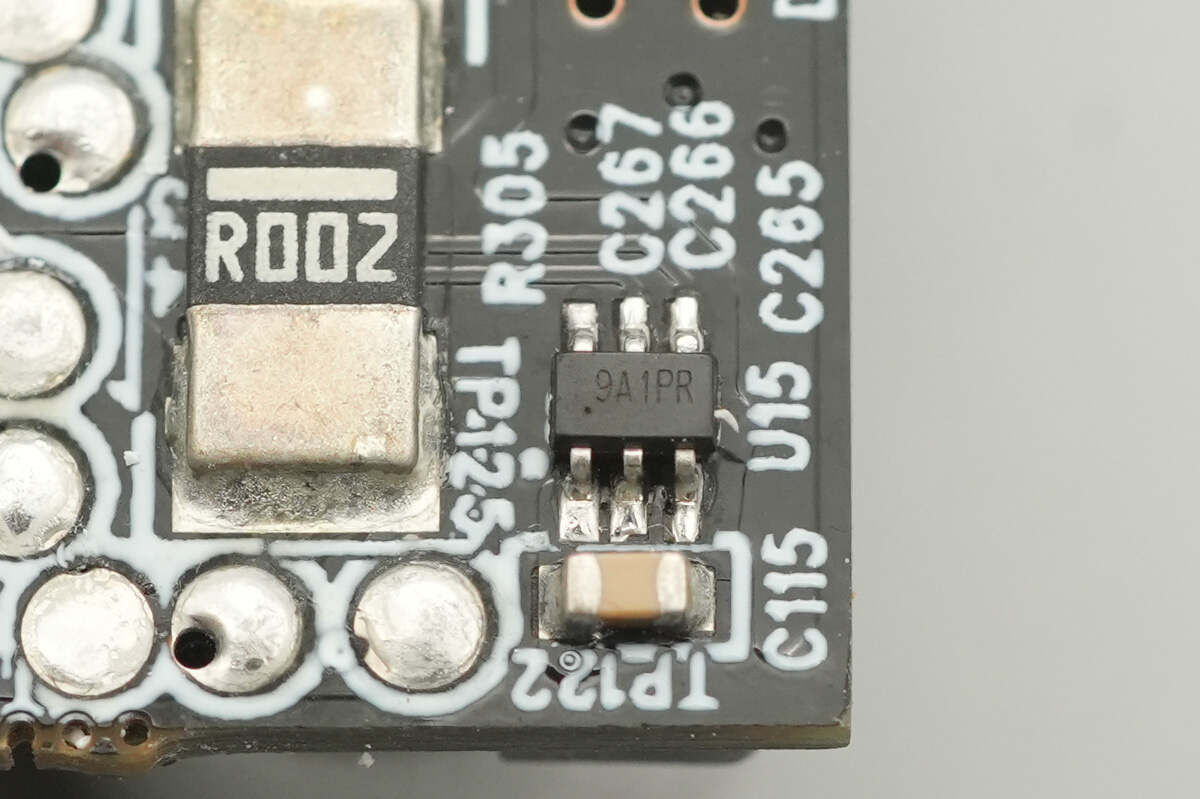
The current sensing chip is from 3PEAK, marked with 9A1, model TP181A1. It is a zero-drift, bidirectional current sense amplifier, packaged in SC70.
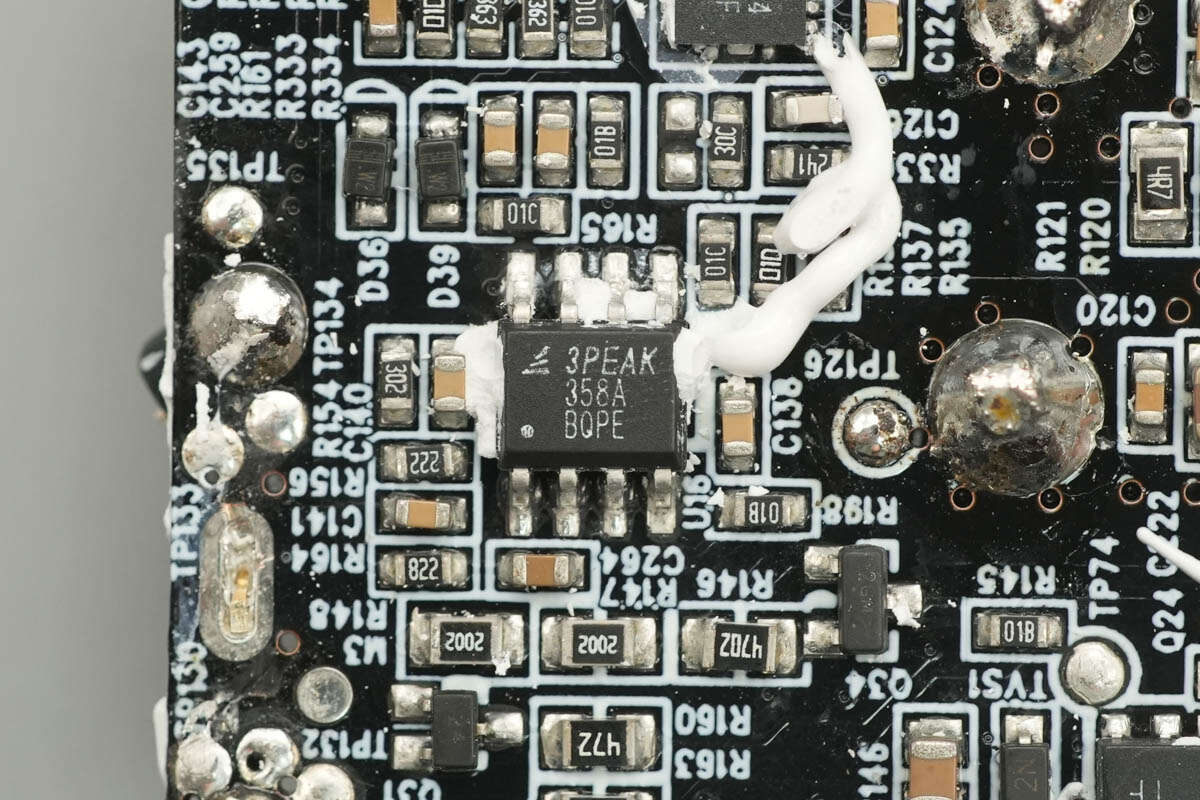
The operational amplifier is from 3PEAK, model LM358A. It is a high-voltage amplifier featuring low offset, low power consumption, and stable frequency response, packaged in SOP-8.
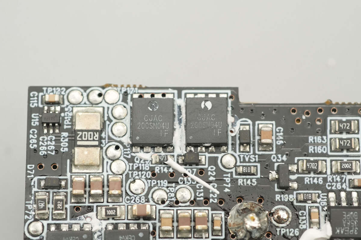
The output control MOSFETs are from JSCJ, model CJAC200SN04U. They are NMOS devices rated at 40V with an Rds(on) of 0.67 mΩ, packaged in PDFNWB 5×6-8L.
The output fuse is rated at 20A.
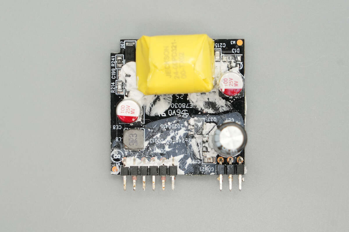
The auxiliary power PCB includes filter capacitors, a transformer, and a buck inductor.
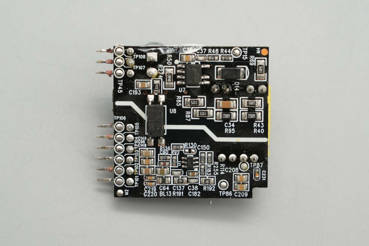
The back side features a power IC, feedback optocoupler, and a synchronous buck converter.
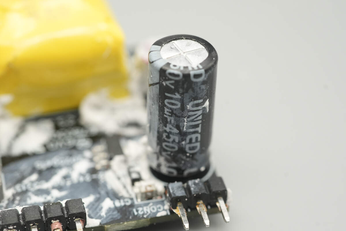
The filter capacitor has a specification of 10 μF, 450 V.
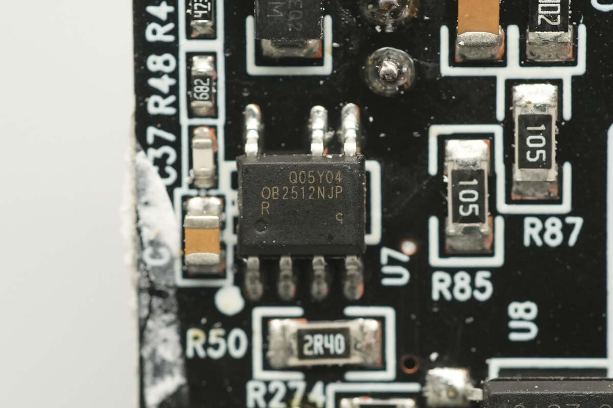
The primary power chip is from On-Bright, model OB2512RN. It is a high-performance offline power IC featuring primary-side feedback, an integrated controller, and a MOSFET, packaged in SOP-7.
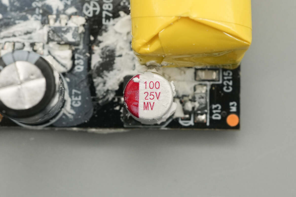
The filter capacitor has a specification of 100 μF, 25 V.
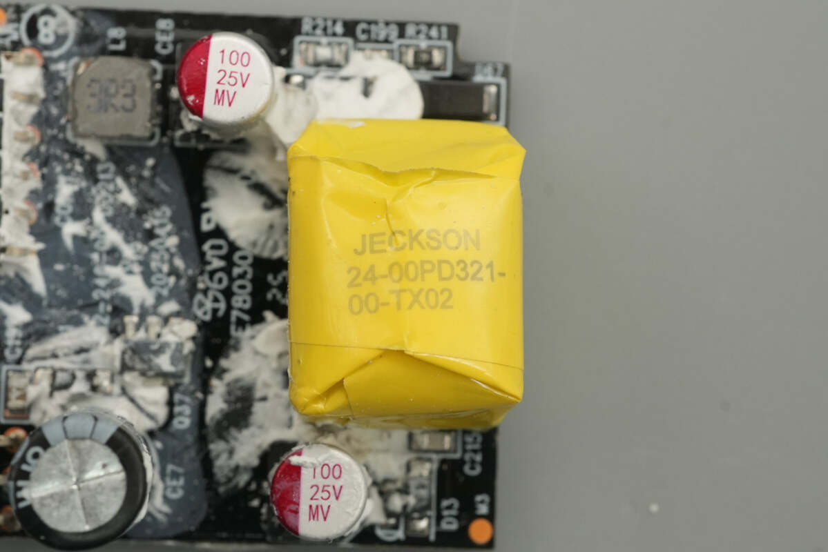
The transformer is tightly wrapped with insulating tape.
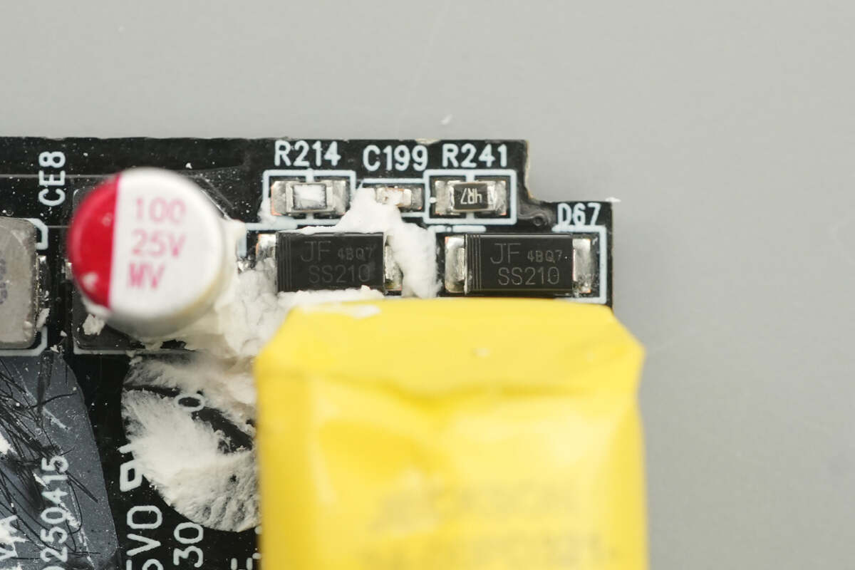
Two rectifiers, model SS210, rated at 2A, 100V.
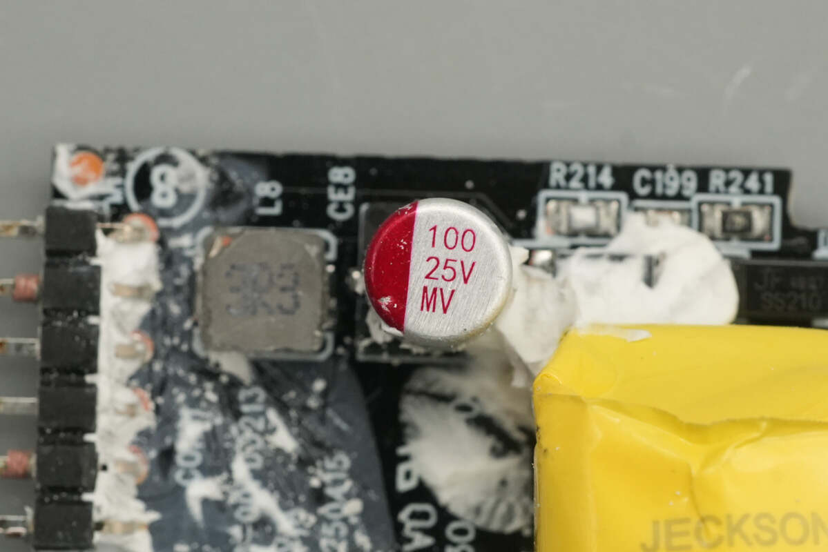
The filter capacitor has a specification of 100 μF, 25 V.

The synchronous buck chip is from SILERGY, marked with Iu, model SY8301. It features an integrated MOSFET, supports a maximum input voltage of 40V, delivers an output current of 1A, and is packaged in SOT23-6.
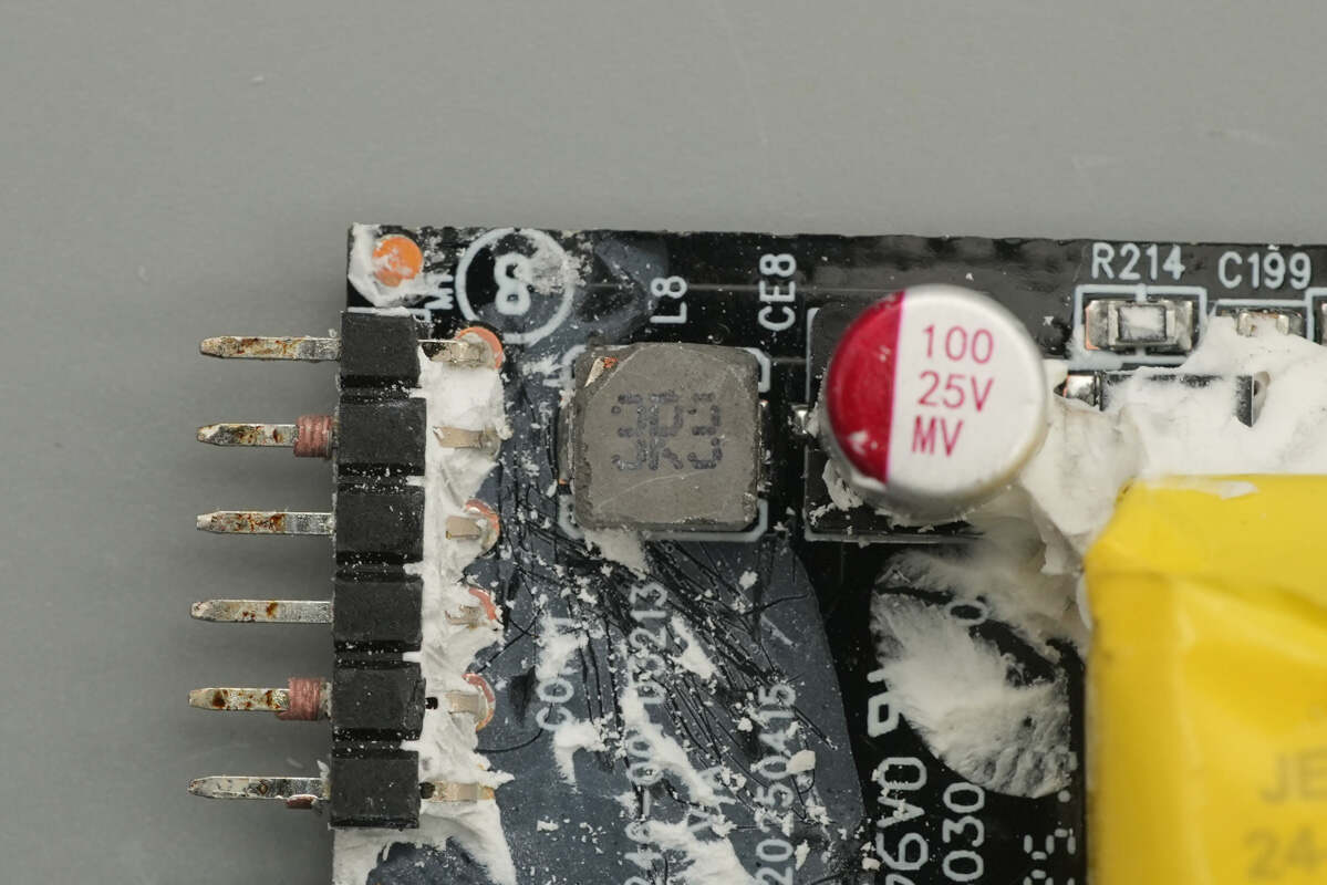
Close-up of the 3.3 μH buck inductor.
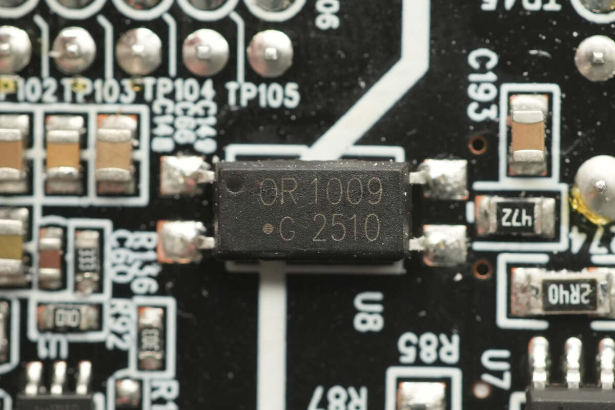
The OR OR1009 optocoupler is used for feedback control.
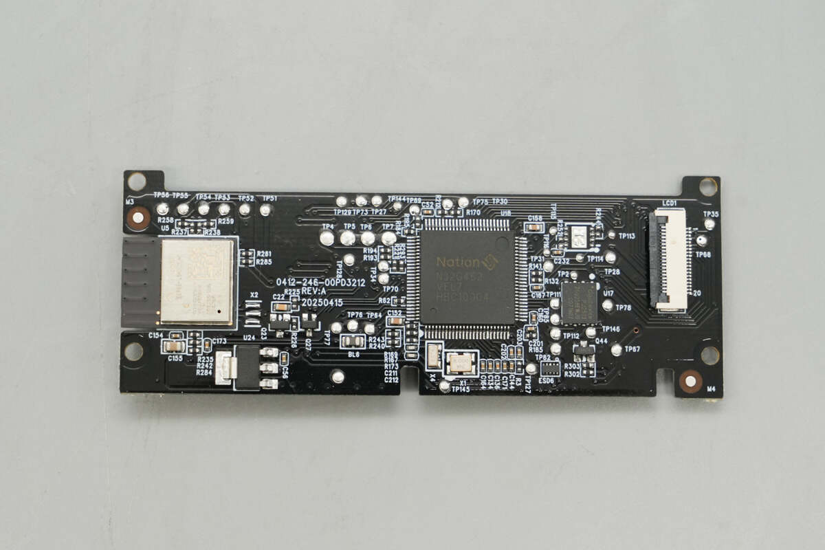
The left side of the display driver PCB houses the wireless communication module, voltage regulator, MCU, and memory.
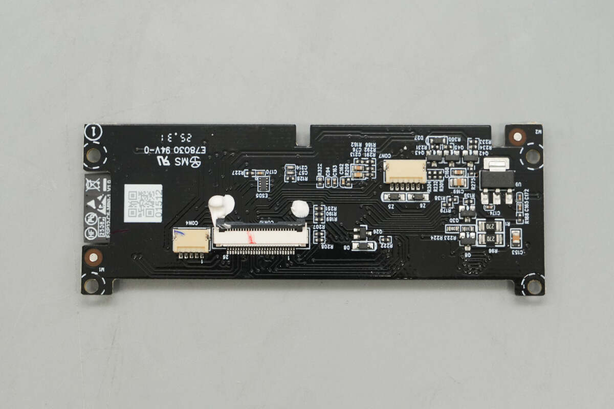
The back side of the PCB is equipped with a voltage regulator chip.
The MCU is from Nations, model N32G452VEL7. It features a 32-bit ARM Cortex-M4F core running at 144 MHz, with 512 KB FLASH and 144 KB SRAM. The device supports UART, SPI, QSPI, I2C, USB 2.0, CAN, SDIO, and XFMC interfaces. It is packaged in LQFP-100.

Close-up of the 8.000 MHz SMD crystal oscillator.
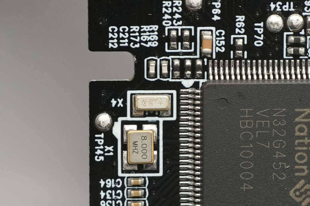
Close-up of the 32.768 kHz SMD crystal oscillator.
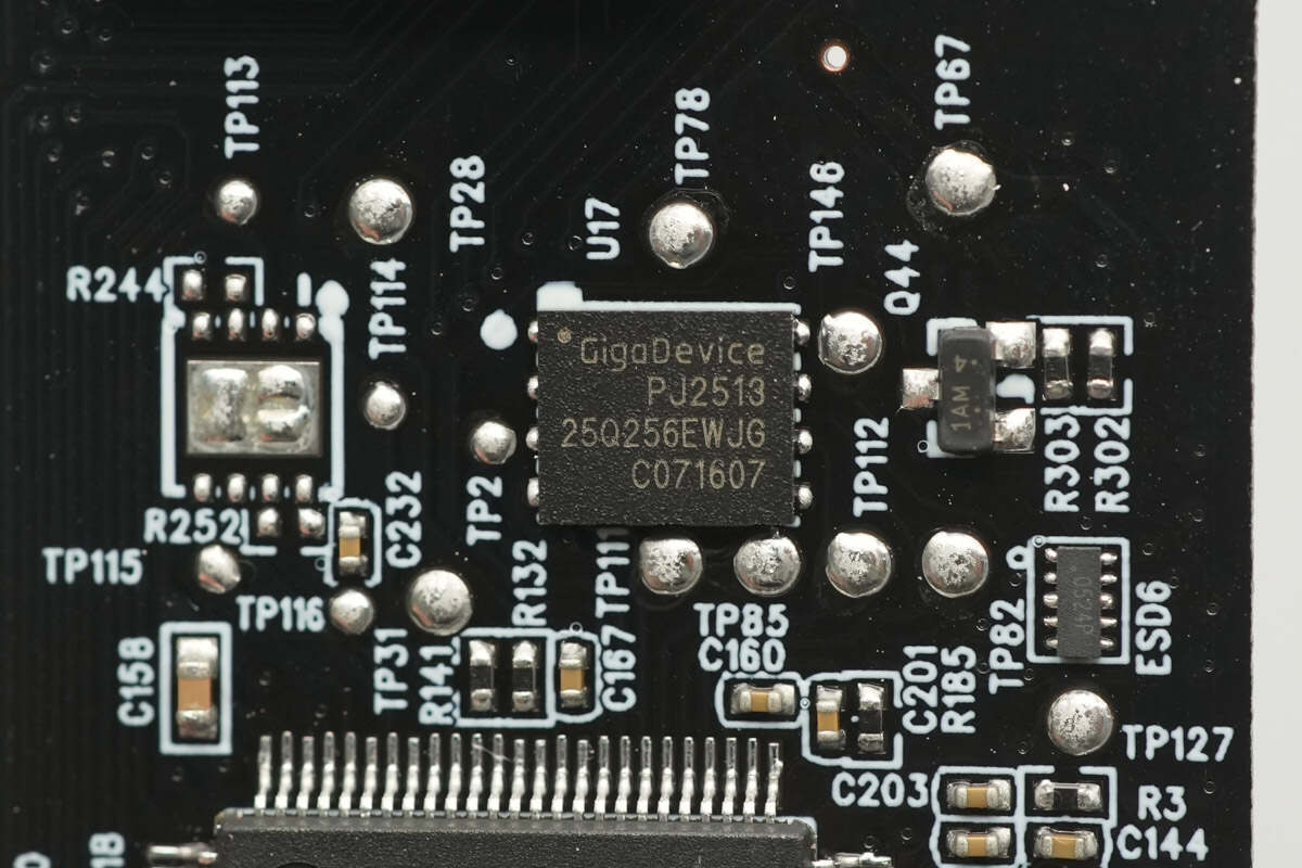
The memory is from GigaDevice, model GD25Q256EWJG, with a capacity of 32MB. It supports an operating voltage of 2.7–3.6V and is packaged in WSON8.

The wireless communication module is from ESPRESSIF, model ESP32-C6-MINI-1. It supports 2.4 GHz WiFi 6, Bluetooth BLE, Zigbee, and Thread. It integrates the ESP32-C6 chip and features an onboard PCB antenna design.
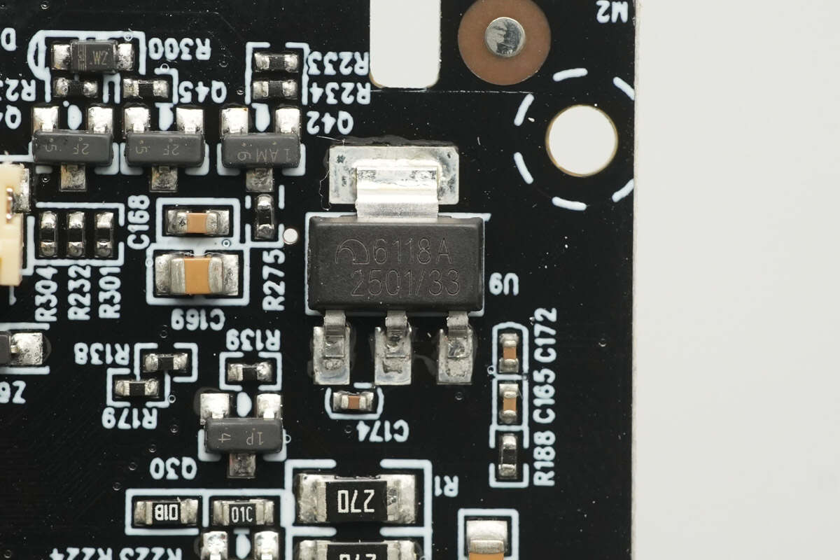
The voltage regulator chip is from Microne, model ME6118A33B3. It supports an input voltage range of 2.5–18 V, delivers a maximum output current of 1A, and is packaged in SOT-223.
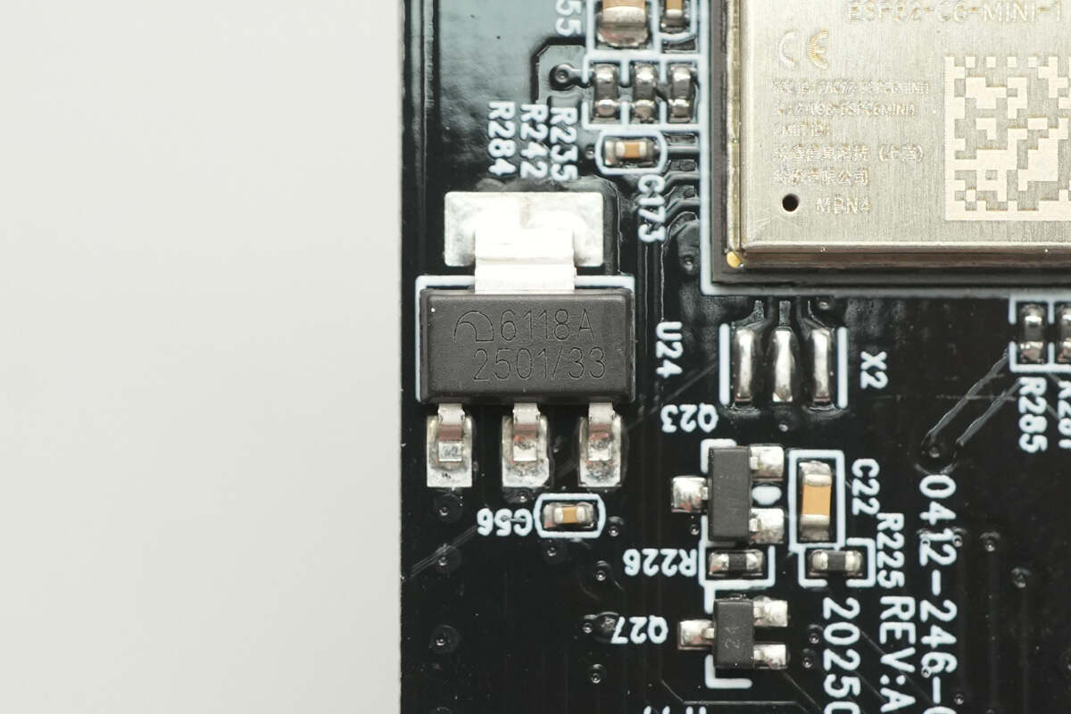
The other voltage regulator chip has the same model.
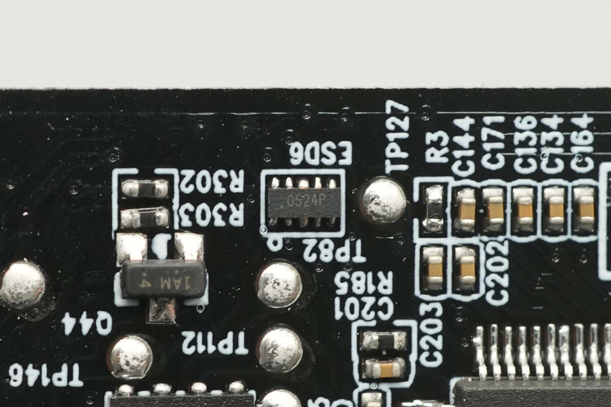
Close-up of the TVS array marked with 0524P.
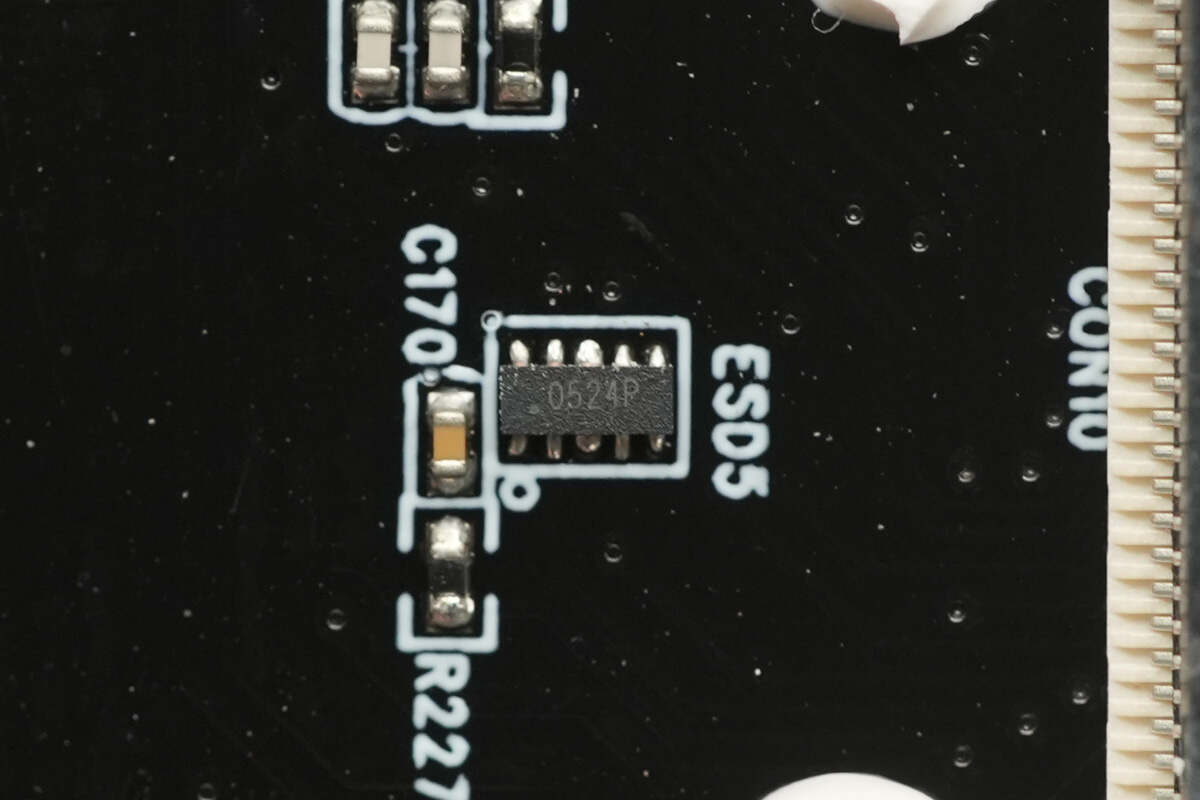
The other TVS array has the same model.
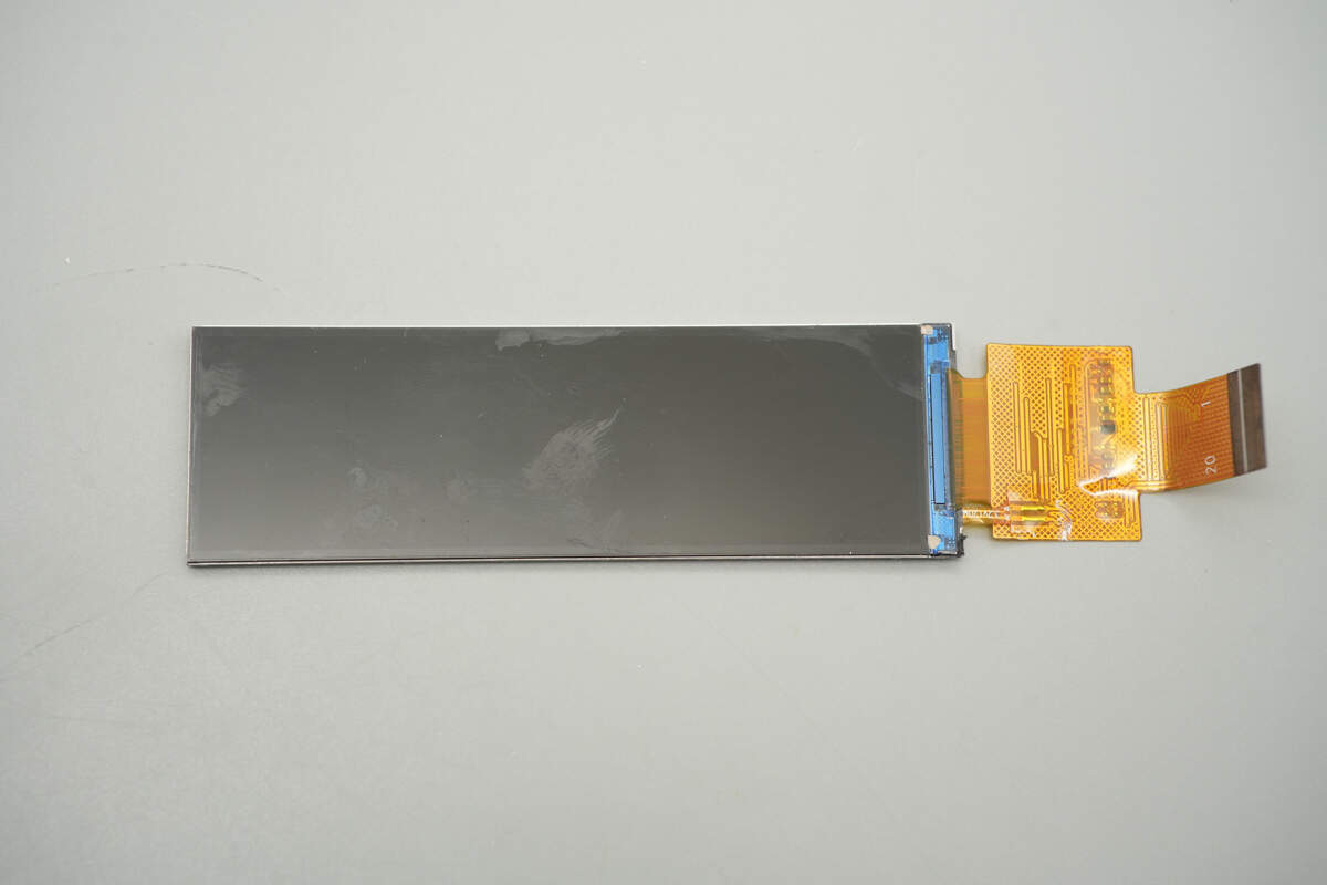
The LCD screen is connected via a flat ribbon cable.

Well, those are all components of the EcoFlow RAPID Pro 320W GaN Desktop Charger.
Summary of ChargerLAB
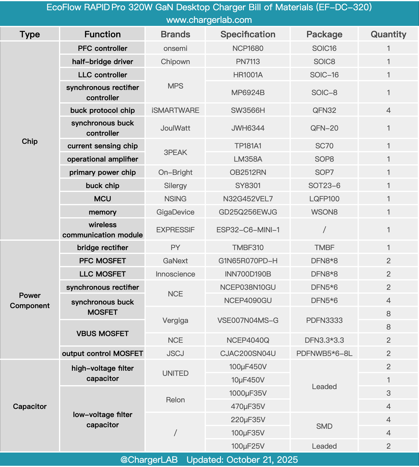
Here is the component list of the EcoFlow RAPID Pro 320W GaN Desktop Charger for your convenience.
It features four USB-C ports and one USB-A port. The top has a Pogopin magnetic connector. Both USB-C1 and USB-C2 support 140W fast charging, while the magnetic connector supports up to 320W output power. The screen displays the clock, standby interactive emojis, and charging animations, and supports app monitoring and deep customization.
After taking it apart, we found that it is composed of multiple PCBs soldered together. The PFC controller is an Onsemi NCP1680, paired with a Chipown PN7113 half-bridge driver and GaNext G1N65R070PD-H GaN FETs. The LLC controller is an MPS HR1001A, paired with Innoscience INN700D190B GaN FETs.
The synchronous rectifier controller uses an MPS MP6924B, paired with NCE NCEP038N10GU synchronous rectifiers. The buck output employs iSmartWare SW3566H buck protocol chips combined with Vergiga VSE007N04MS-G MOSFETs. A Nations N32G452VEL7 MCU handles parameter acquisition and function display. The PCBA modules feature thermal pads and heat sinks, with components reinforced and thermally secured using adhesive, demonstrating solid craftsmanship and reliable materials.
Related Articles:
1. Teardown of MEGMEET 600W Switching Power Supply (MSP600)
2. Teardown of vivo 120W Multi-Port GaN Charger (V12060L0D0-CN)
3. Teardown of Xiaomi 30W 2-in-1 Magnetic Wireless Charger (MDY-20-EC)