Introduction
Today, we're going to tear down a power adapter from Delta. This adapter not only comes with a built-in USB-C cable but also supports PD 3.1 with up to 240W output—something that's rare on the market. In addition, it features a dual-material design using both GaN and SiC, offering improved reliability and efficiency compared to traditional power supplies. That makes it well worth a teardown and a detailed introduction for everyone, so let’s dive in and take a closer look.
Product Appearance
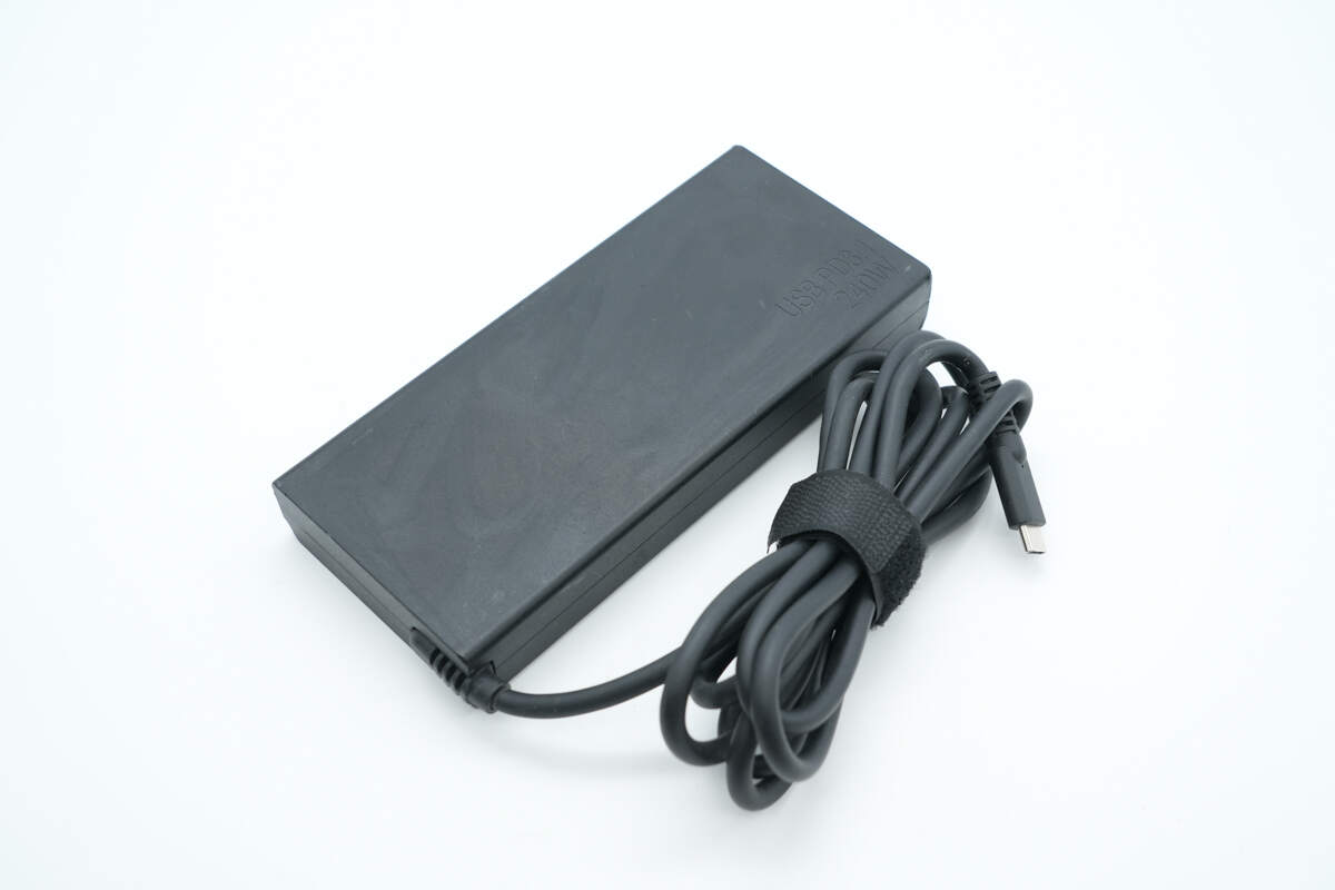
It features a traditional design with a matte-finish casing. The input power cord uses a detachable design, while the output USB-C cable is integrated into the adapter.
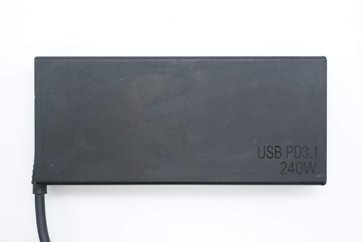
The lower right corner of the top surface is labeled with “240W USB PD3.1.”
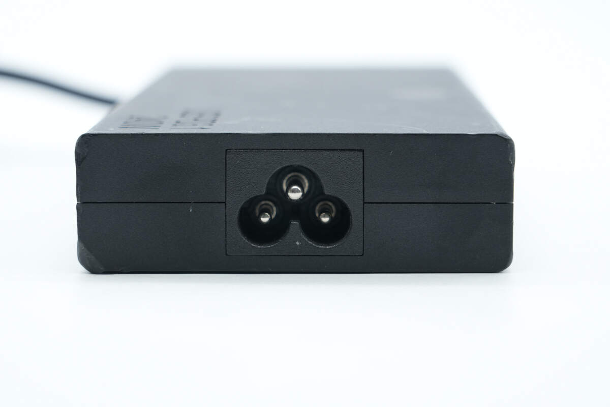
The input interface uses a C5 inlet.
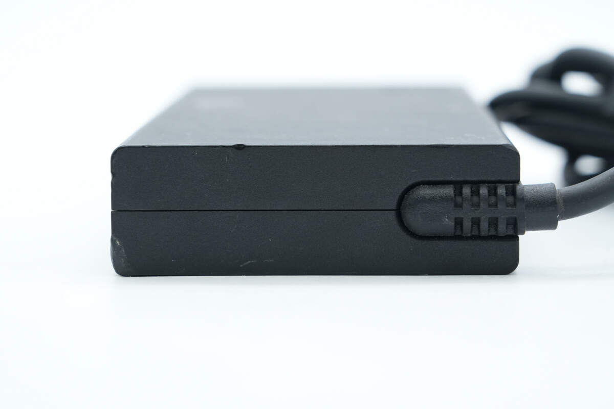
The output cable features a bend-resistant design.
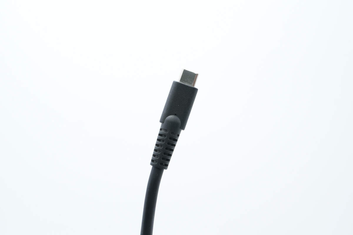
The USB-C plug also features a bend-resistant design.
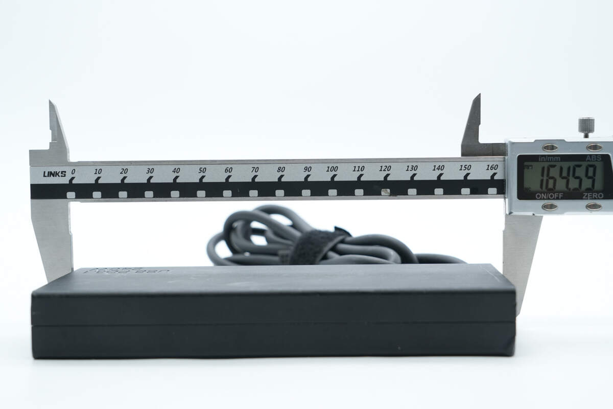
The length of the adapter is about 164.59 mm (6.48 inches).
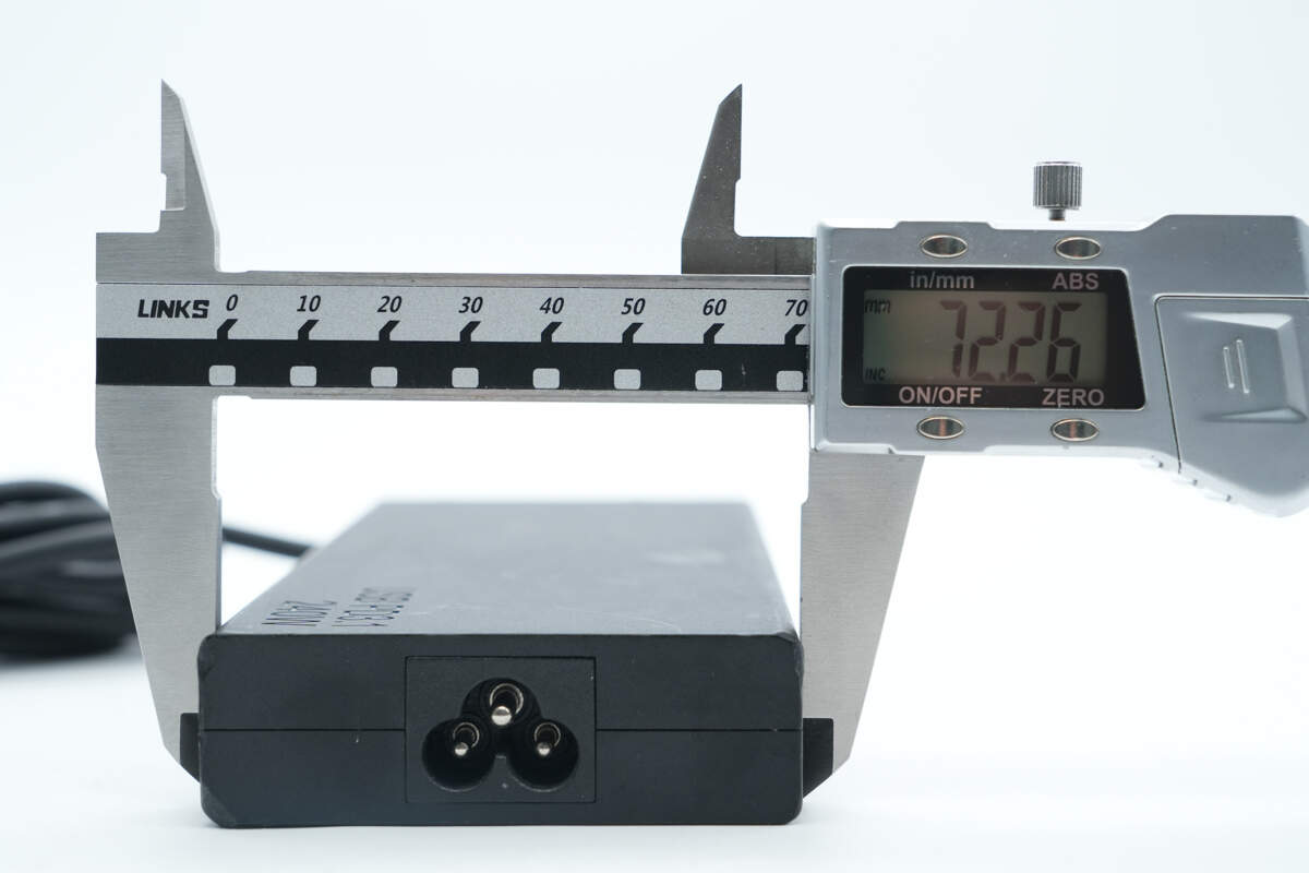
The width is about 72.26 mm (2.84 inches).
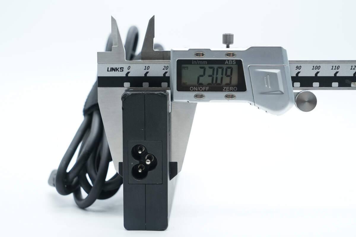
The thickness is about 23.09 mm (0.91 inches).
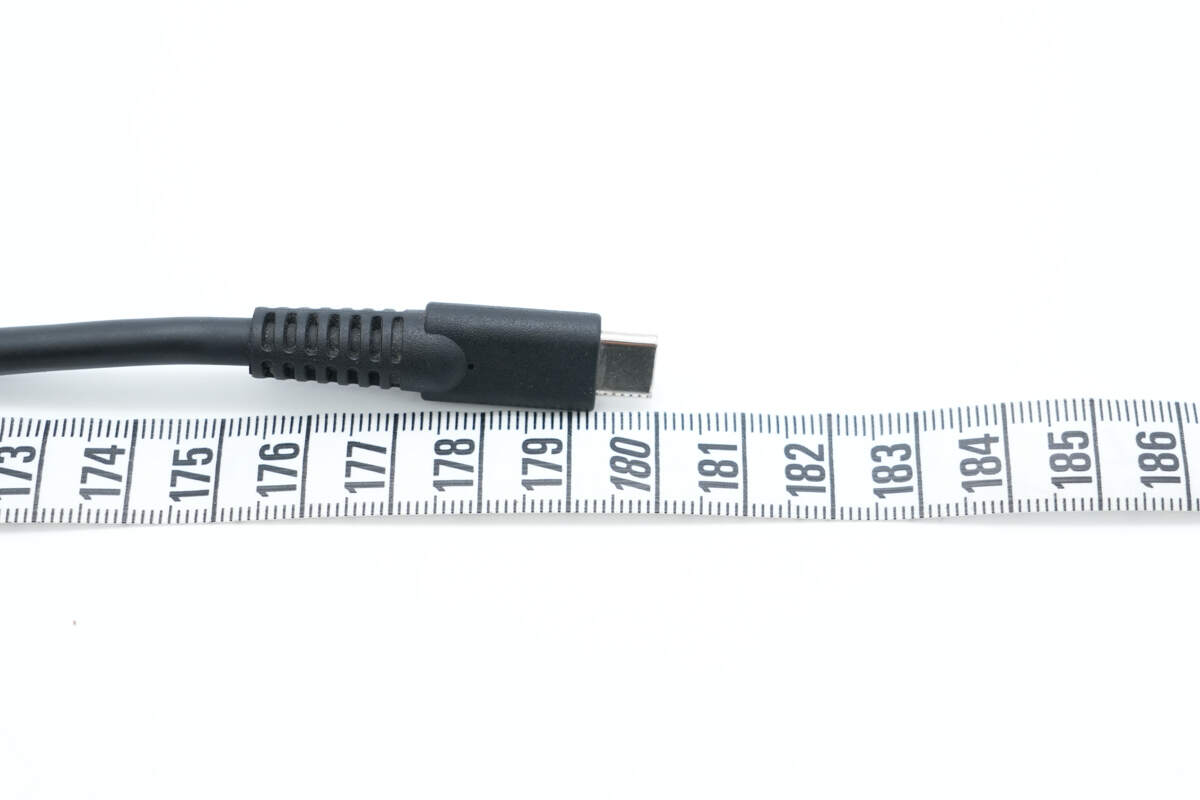
The length of the output cable is about 1.8 meters.

That's how big it is in the hand.
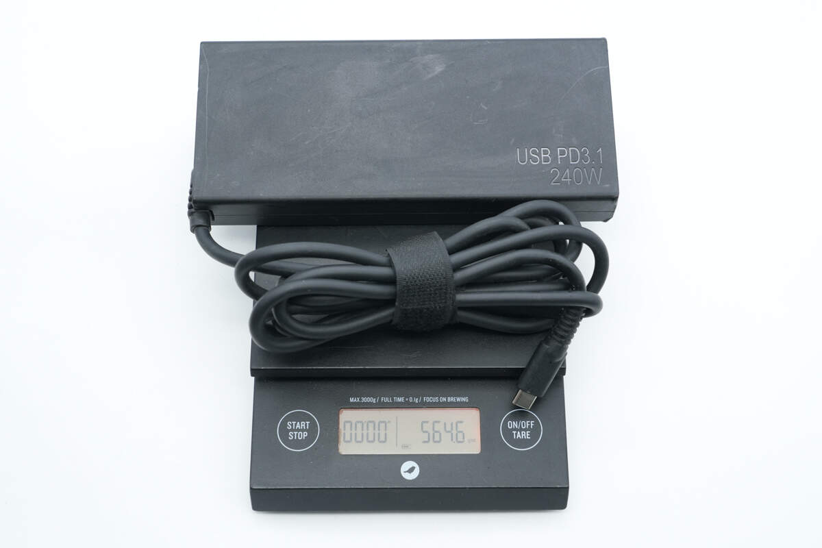
The weight is about 565 g (19.93 oz).
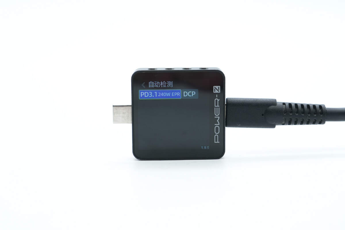
ChargerLAB POWER-Z KM003C shows that the USB-C cable supports PD3.1 and DCP charging protocols.
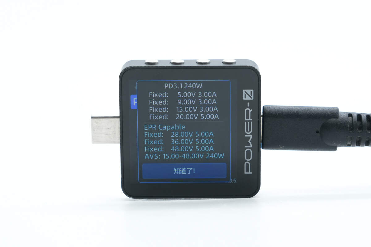
And it has seven fixed PDOs of 5V3A, 9V3A, 15V3A, 20V5A, 28V5A, 36V5A, and 48V5A. It also has one set of AVS, which is 15-48V 240W.
Teardown
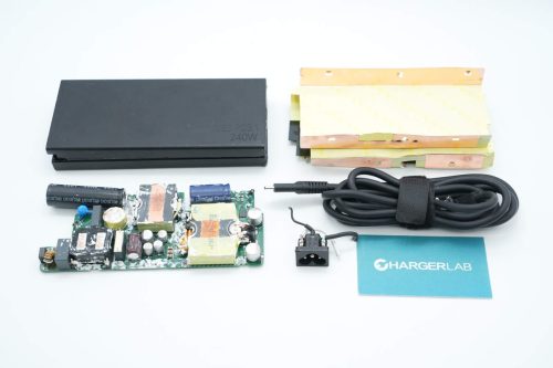
Next, let's take it apart to see its internal components and structure.
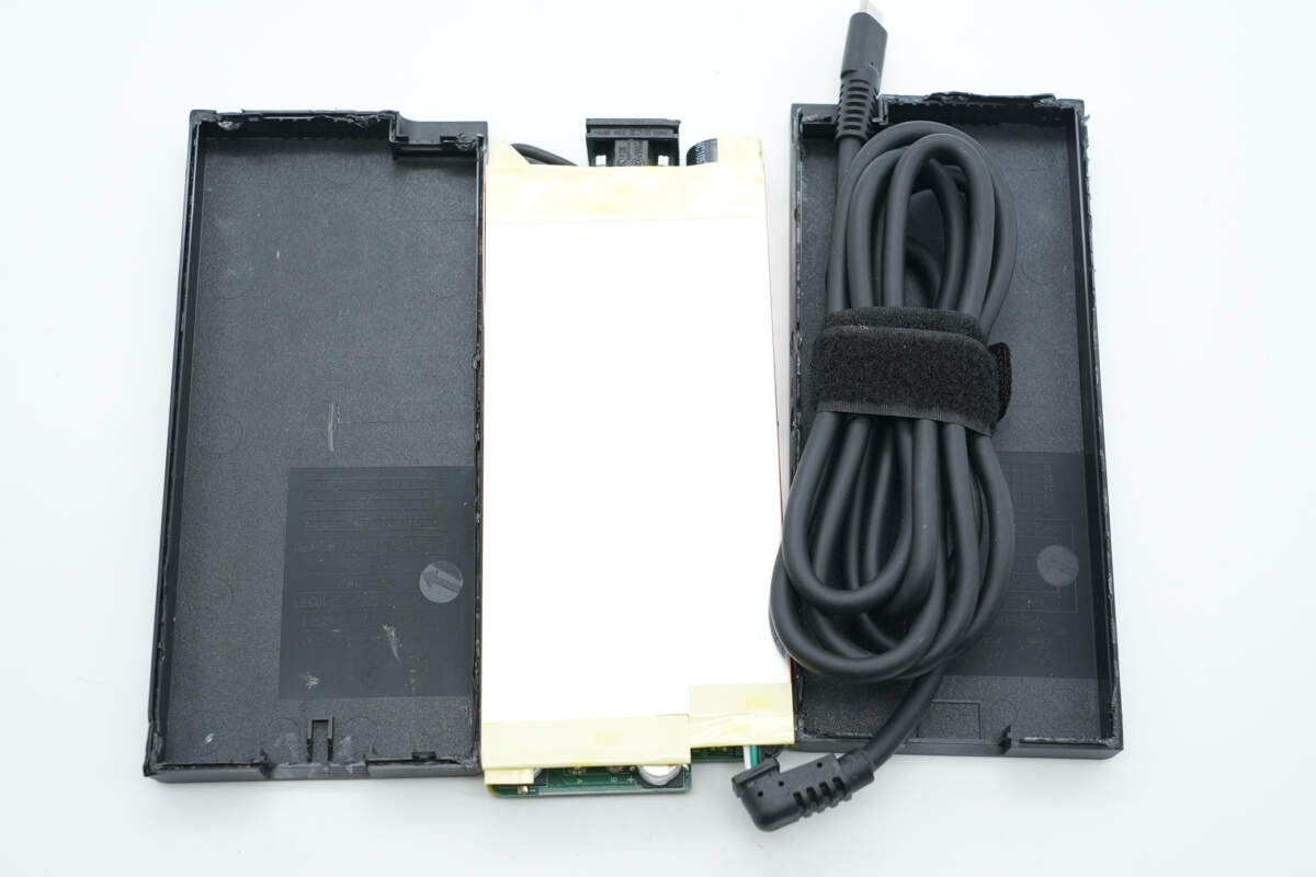
Open the casing. It is assembled using ultrasonic welding.
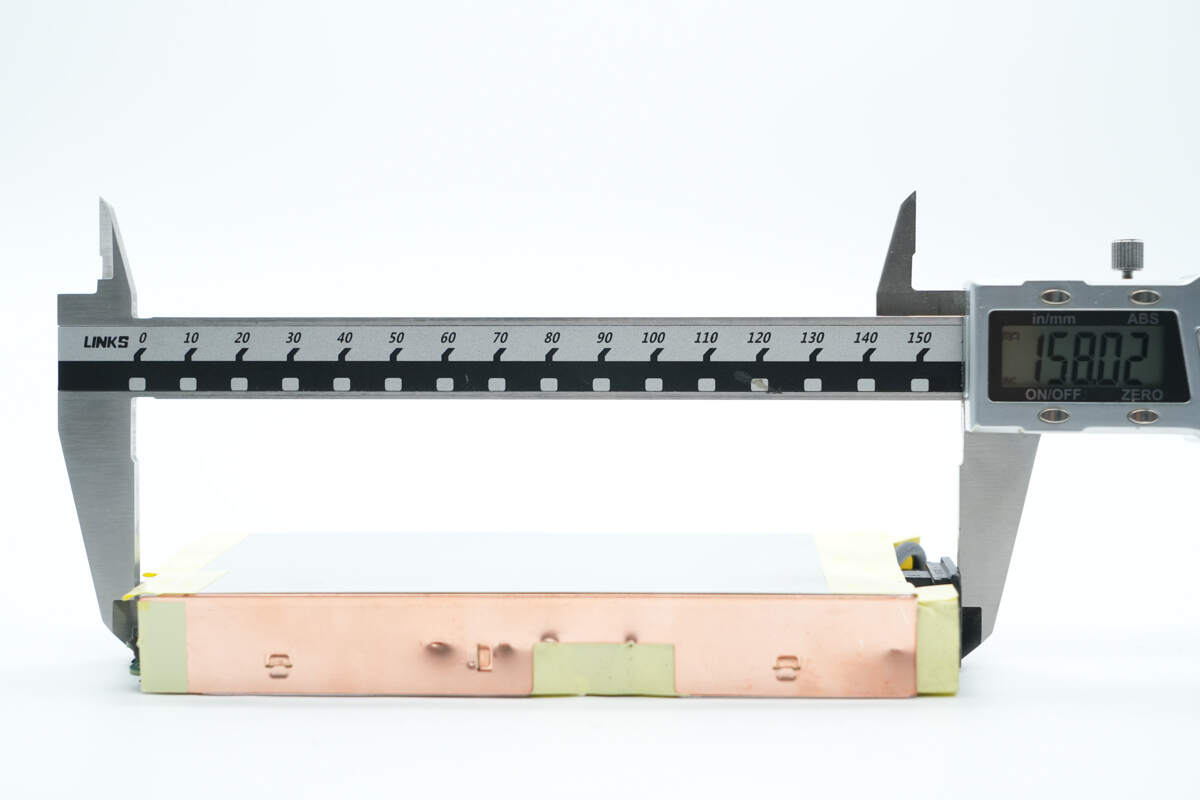
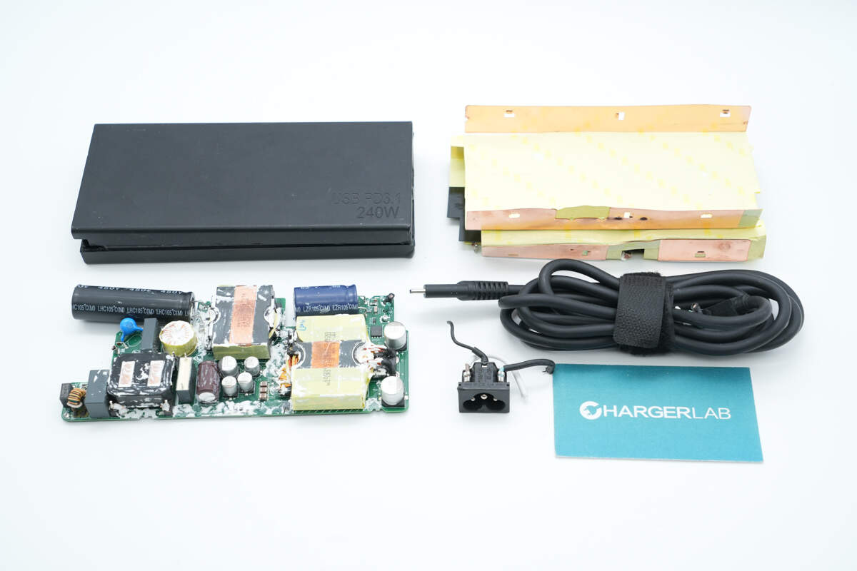
The length of the PCBA module is about 158.02 mm (6.22 inches).
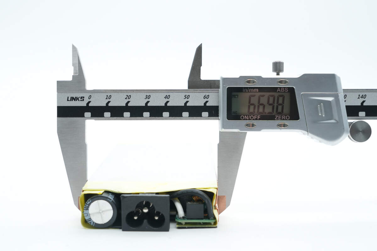
The width is about 66.98 mm (2.64 inches).

The thickness is about 18.39 mm (0.72 inches).
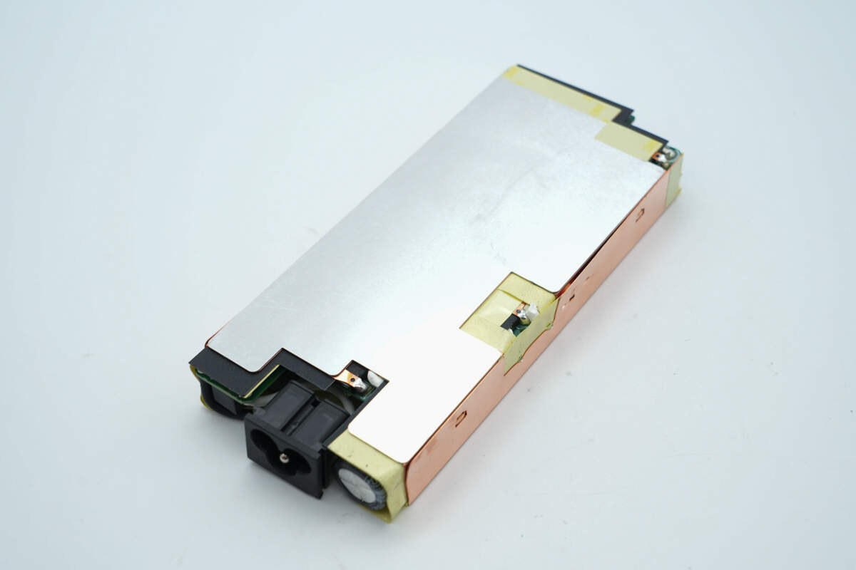
The PCBA module is covered by a metal heat sink, which is secured in place with clips and soldering.
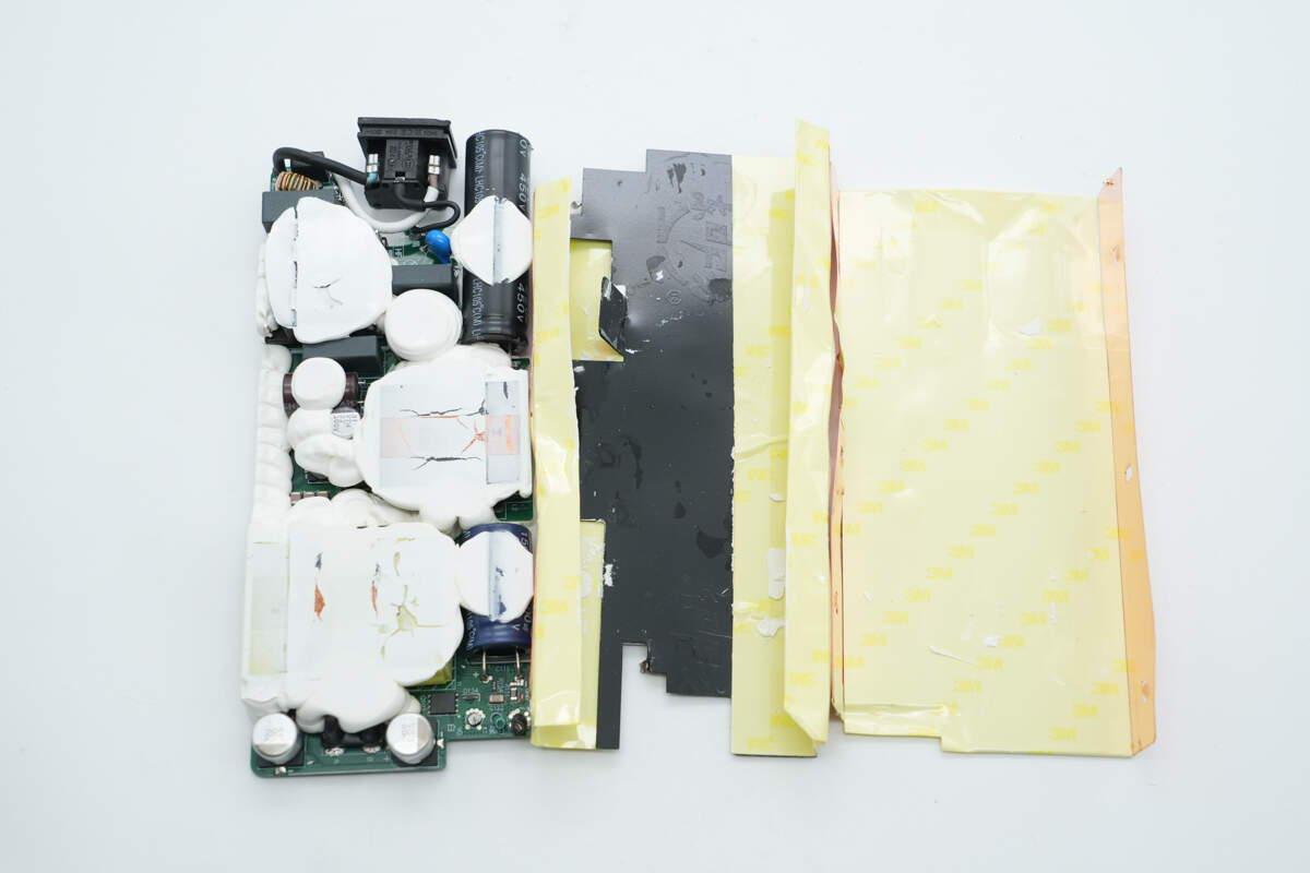
Remove the heat sink. Insulation tape and Mylar sheets are attached to the inside of the heat sink. Capacitors, transformers, and other components are reinforced with white adhesive.
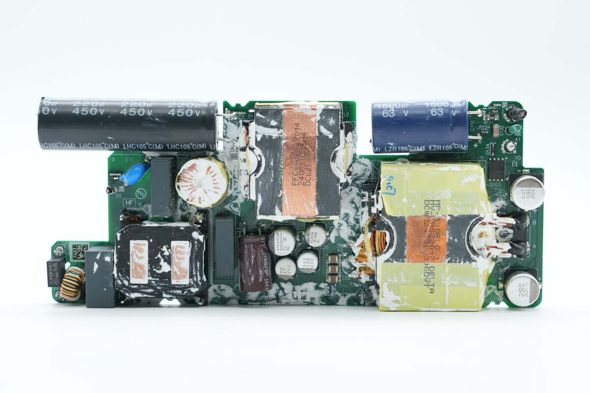
After removing the white adhesive, the front side of the PCBA module reveals components such as a time-delay fuse, common mode chokes, electrolytic capacitors, a PFC boost inductor, and a transformer.
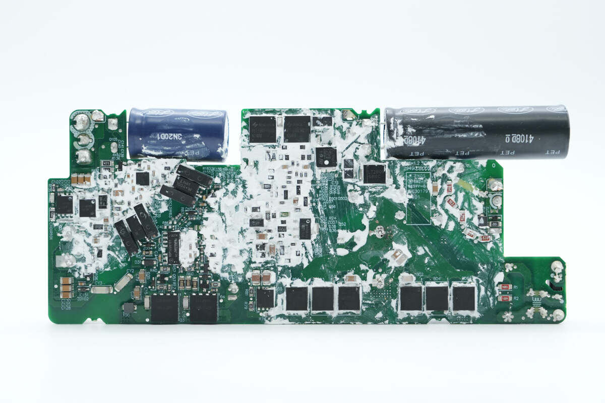
On the back side, components such as bridge rectifiers, the master control chip, PFC MOSFETs, primary MOSFETs, a synchronous rectifier controller, synchronous rectifiers, and the protocol chip are present.
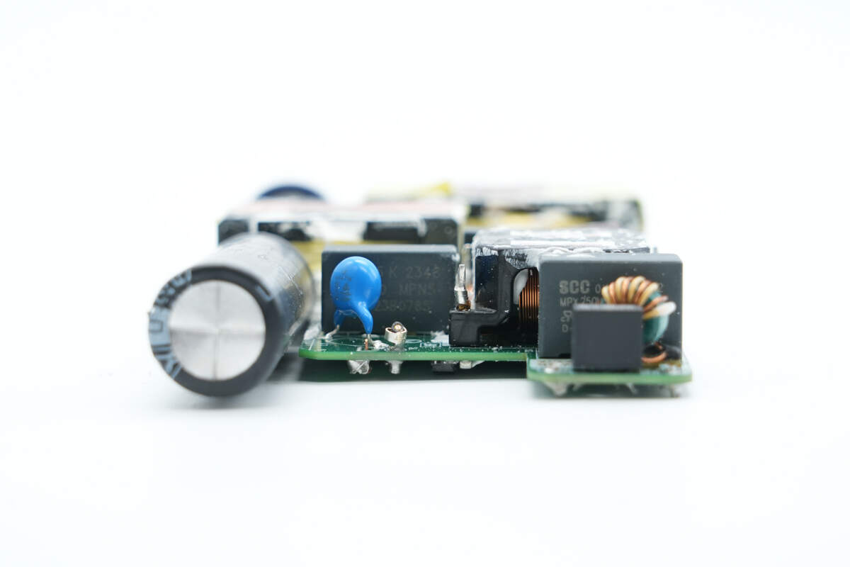
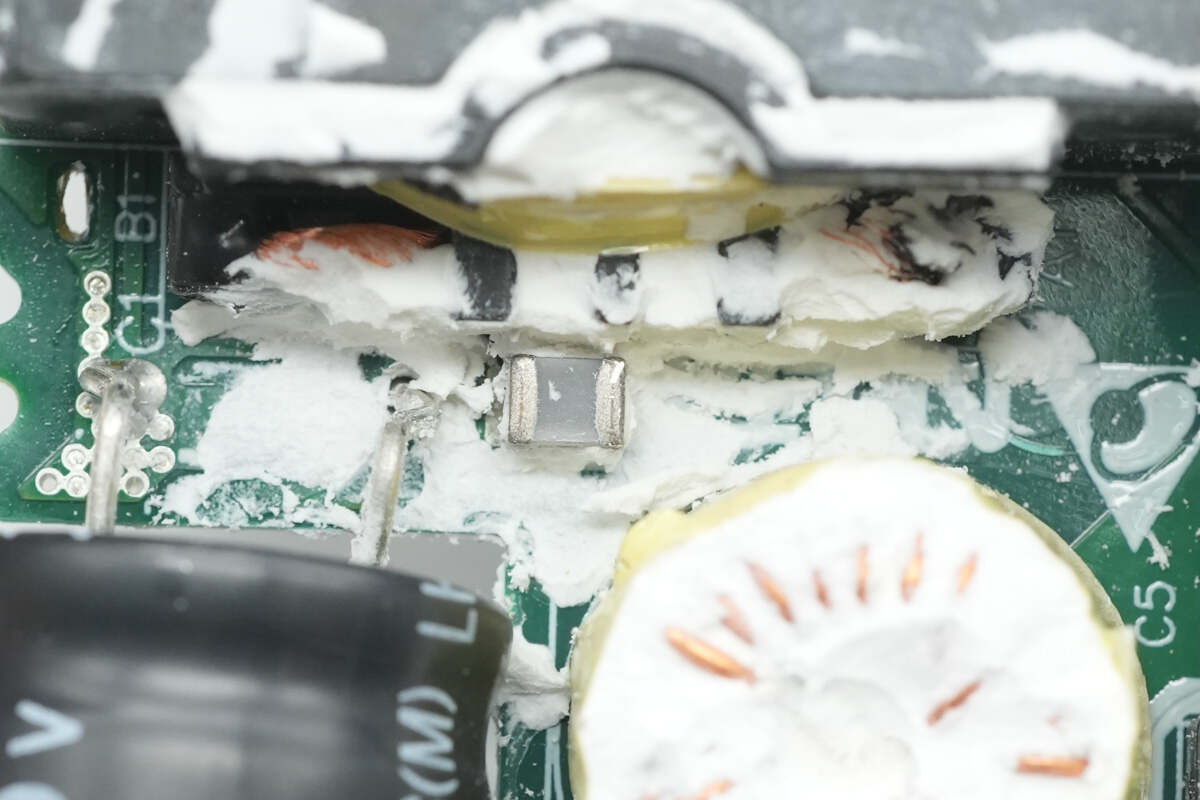
At the front end of the PCBA module, there is a time-delay fuse, common mode chokes, a safety X2 capacitor, blue Y capacitors, and filter capacitors.

The time-delay fuse is rated at 6.3A, 250V.
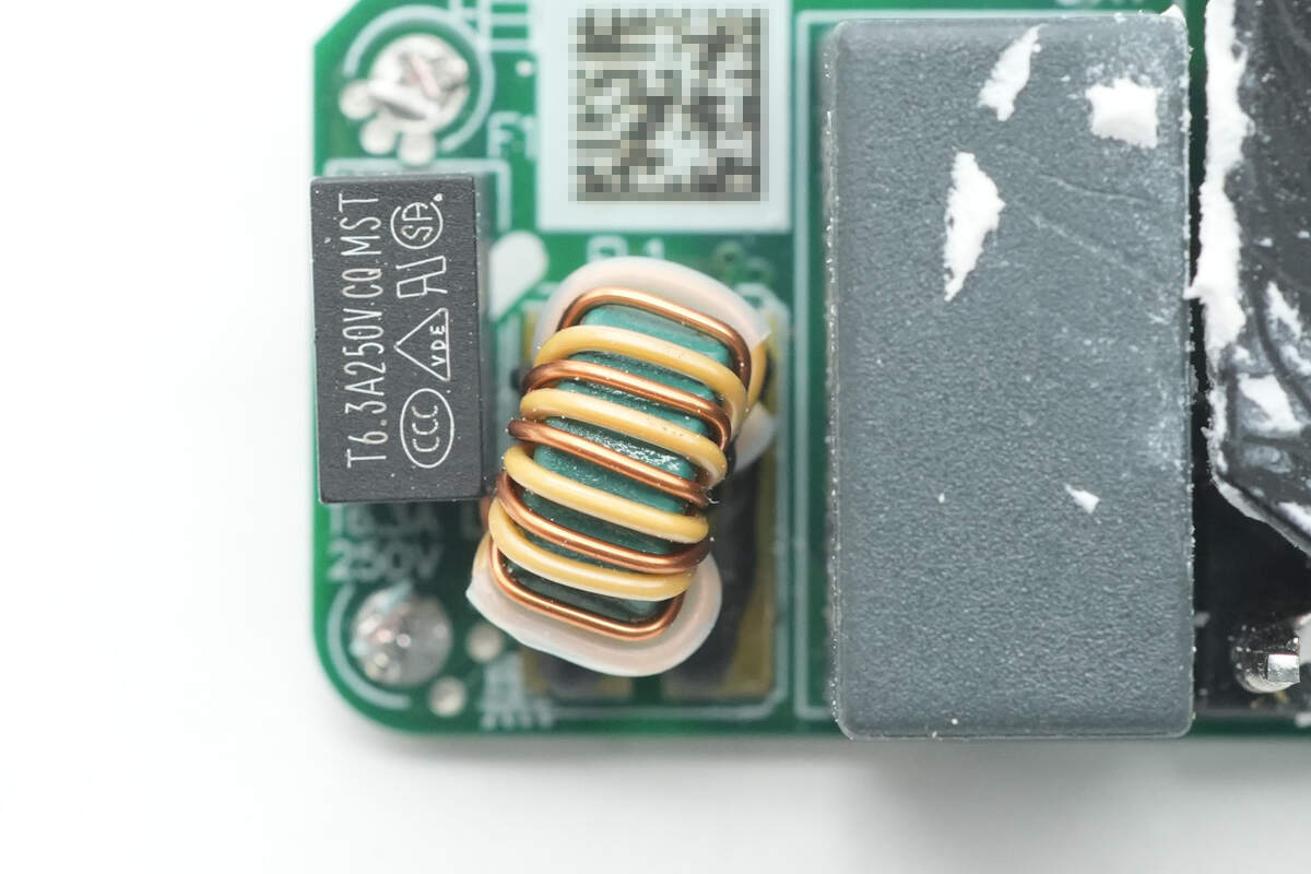
The common mode choke is wound with two wires and is used to filter out EMI interference.
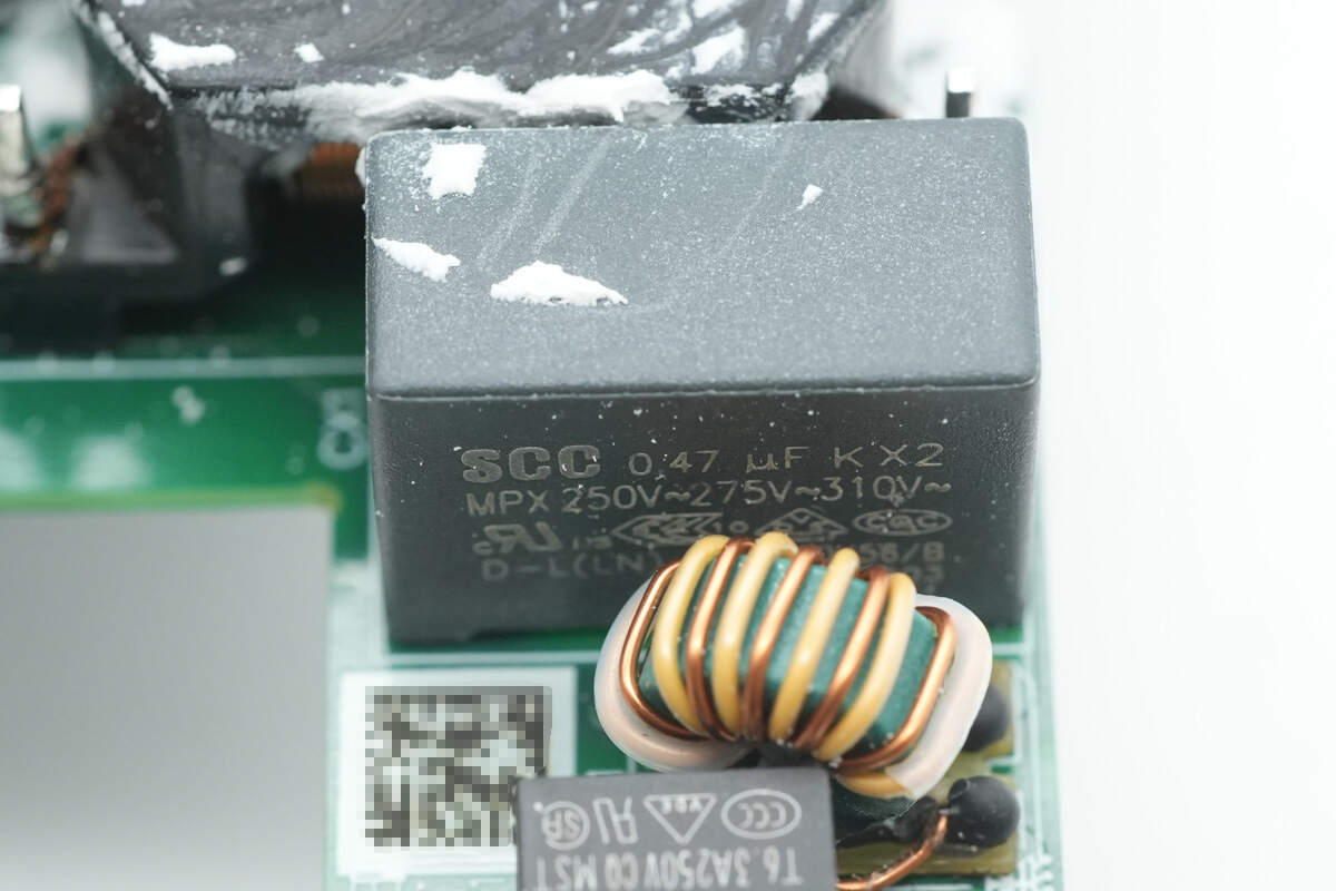
The safety X2 capacitor is from SCC. 0.47μF.
Close-up of the secondary common mode choke.
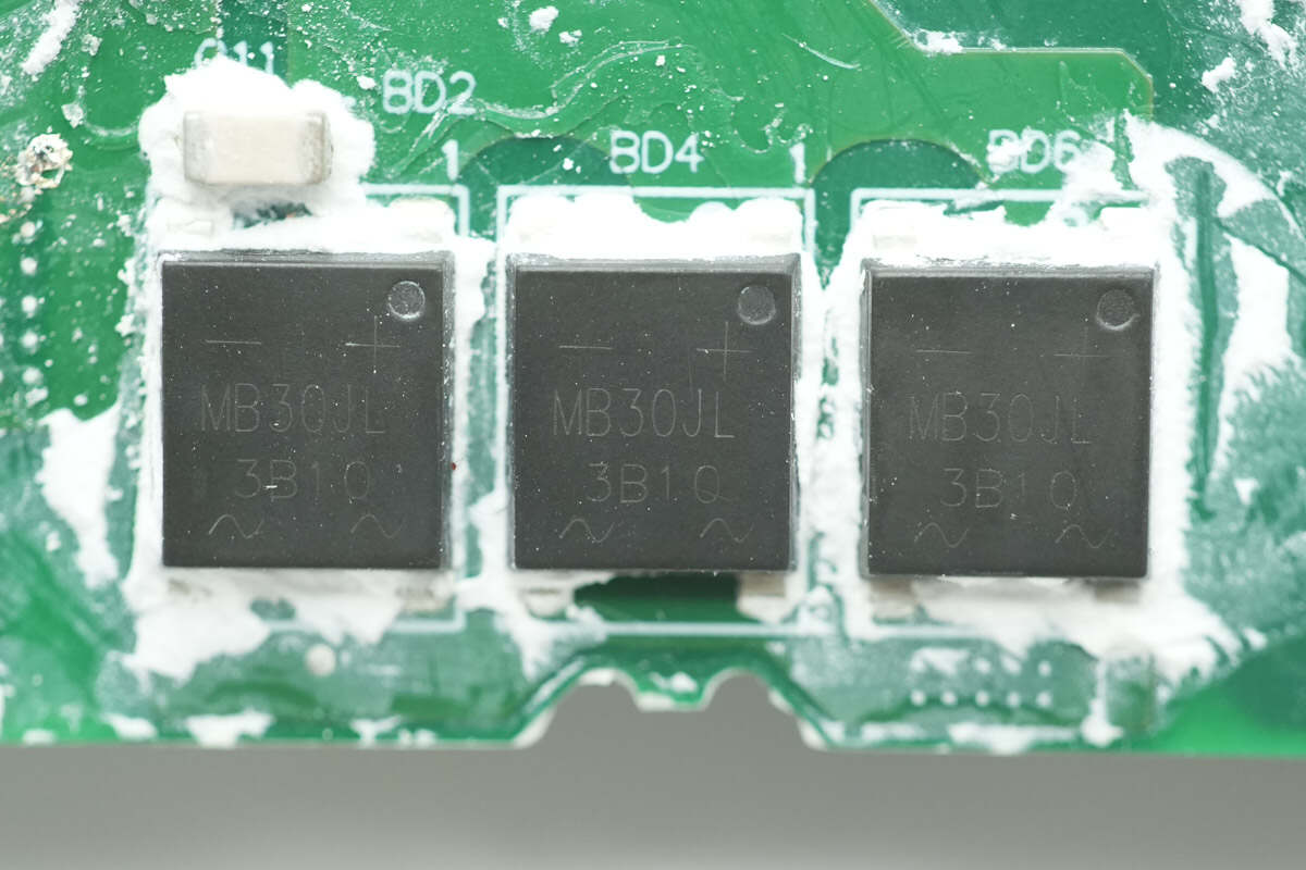
There are three bridge rectifiers marked with MB30JL, each rated for 3A current.

There are another three bridge rectifiers with the same part number.
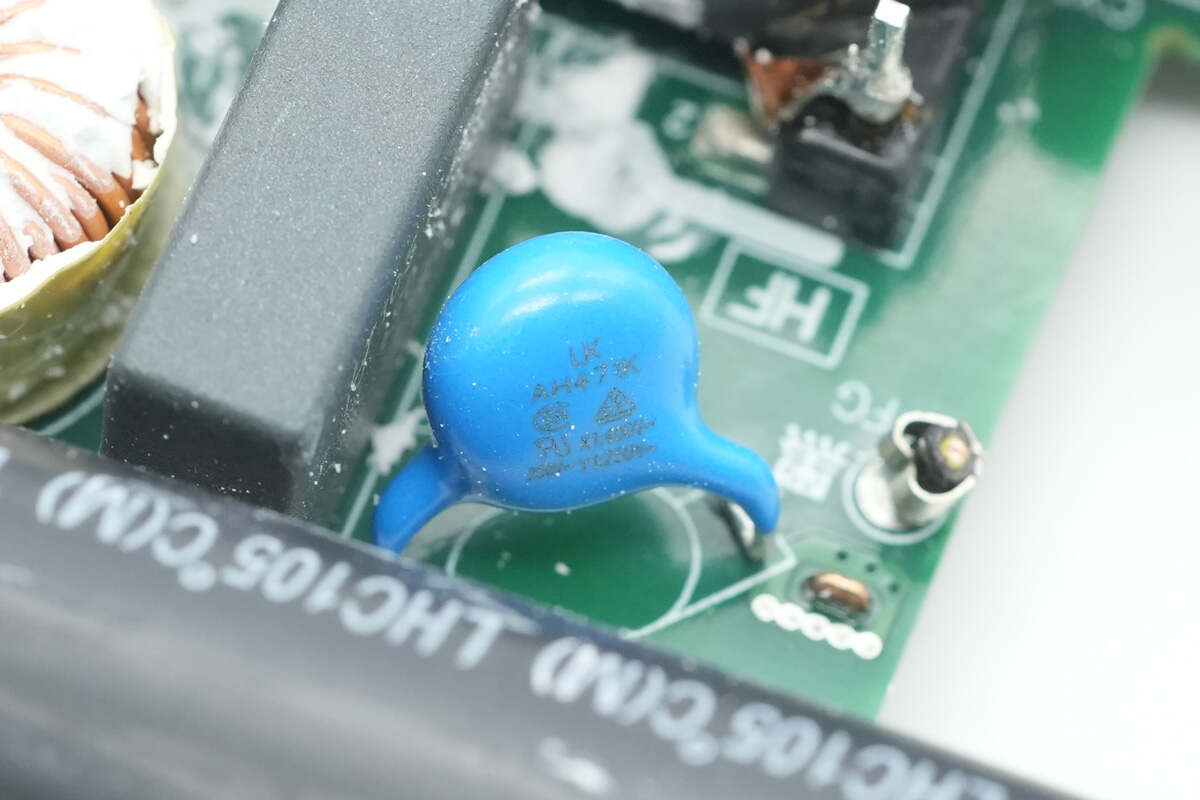
Close-up of the blue Y capacitor.

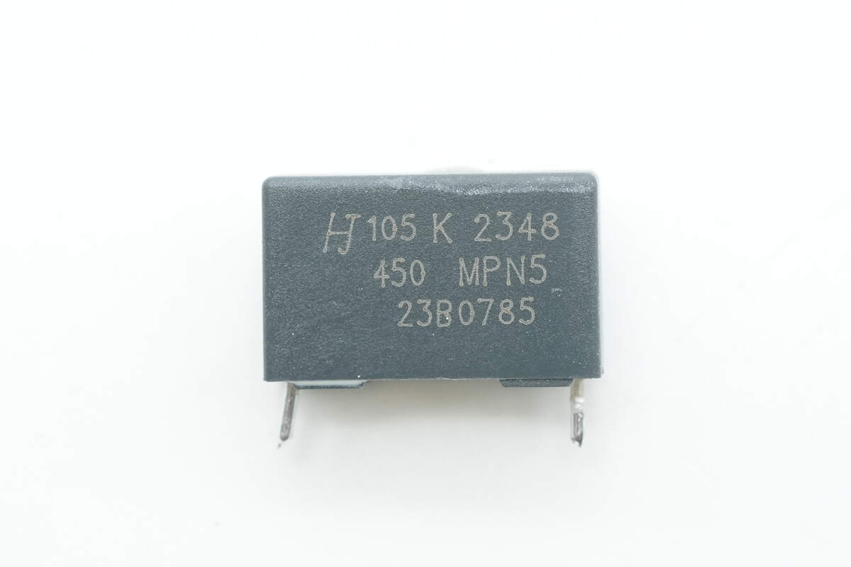
The filter capacitor is from HJC. 1μF 450V.
The filter inductor is wrapped with tape.
Another filter capacitor has the same part number.

The master control chip is from Infineon, marked XDPS2201D1. It is a digital hybrid flyback controller with built-in PFC and LLC controllers. The chip integrates a 600V high-voltage startup circuit and high- and low-side MOSFET drivers. It uses peak current mode control for fast load response and automatically switches to burst mode operation based on output current levels. It supports primary-side overvoltage protection and features standby power consumption under 75mW. Parameters can be configured via a single-pin UART interface. The chip comes in a DSO-14 package and requires minimal external components.
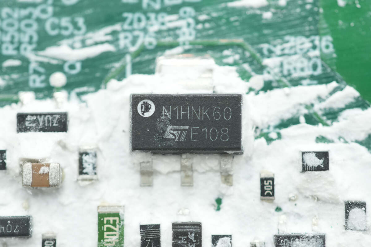
The MOSFET powering the master control chip is from STMicro, model STN1HNK60. It has a voltage rating of 600V and an on-resistance of 8.5Ω, packaged in a SOT-223 case.

The filter capacitor is from AiSHi, rated at 250V, 33μF.
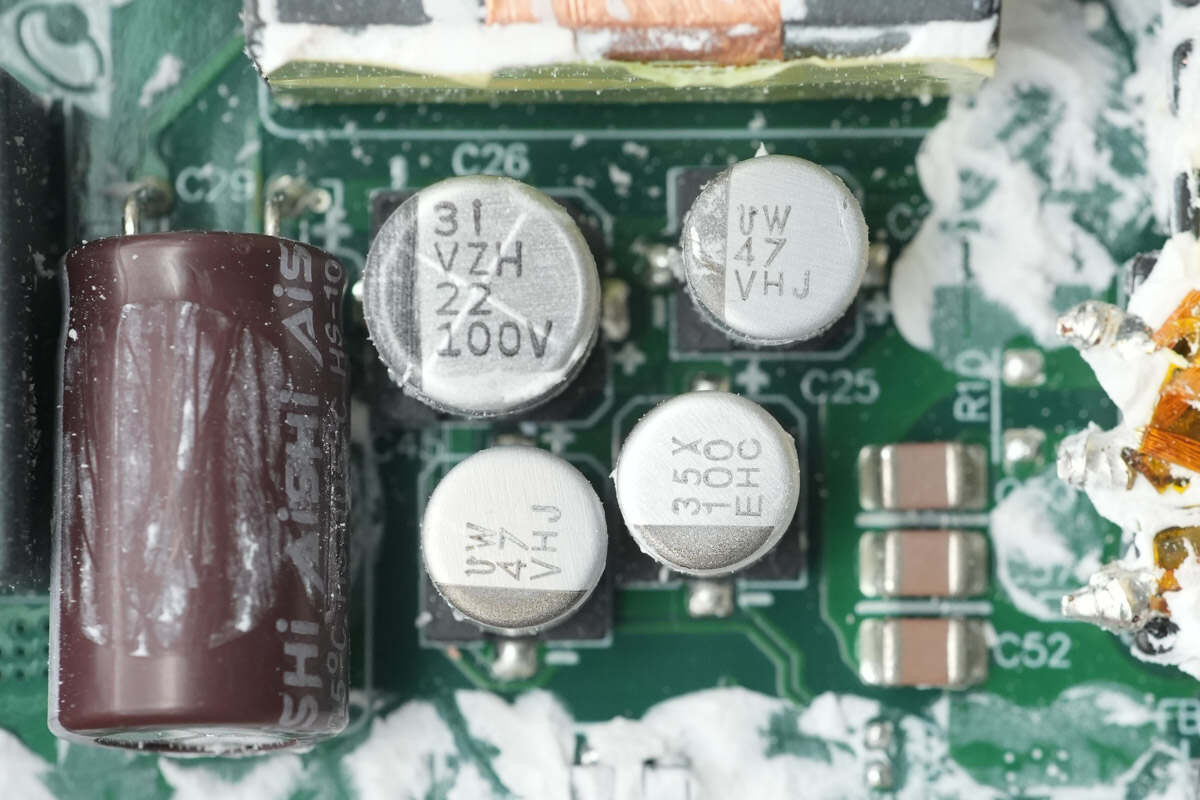
There are four capacitors supplying power to the master control chip. The top-left capacitor is from Lelon, rated at 22μF, 100V. The remaining three are from NCC: the bottom-right one is rated at 100μF, 25V, and the other two are rated at 47μF, 35V.
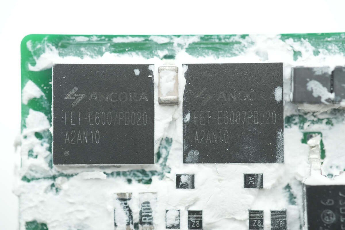
The PFC MOSFETs are from ANCORA, model FET-E6007PB020. These are enhancement-mode GaN FETs with a voltage rating of 650V and an on-resistance of 65mΩ, housed in a PDFN 8×8 package.
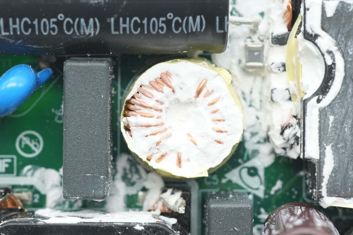
Close-up of the PFC boost inductor.
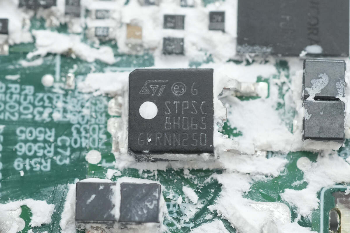
The PFC rectifier is from STMicroelectronics, model STPSC8H065D. It is a 650V, 8A high-surge SiC power Schottky diode in a DPAK package.
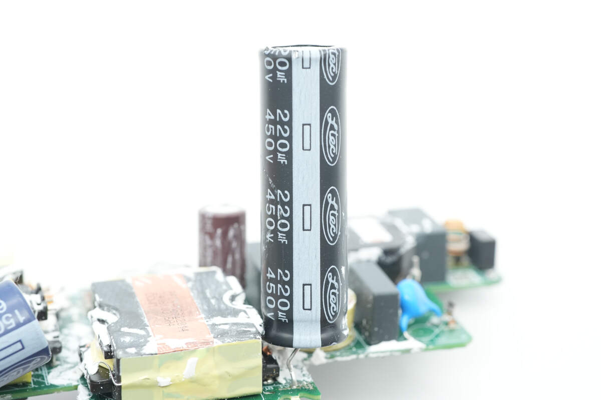
The electrolytic capacitor is from LTEC, with a specification of 450V 220μF.
A close-up of an NPO filter capacitor.
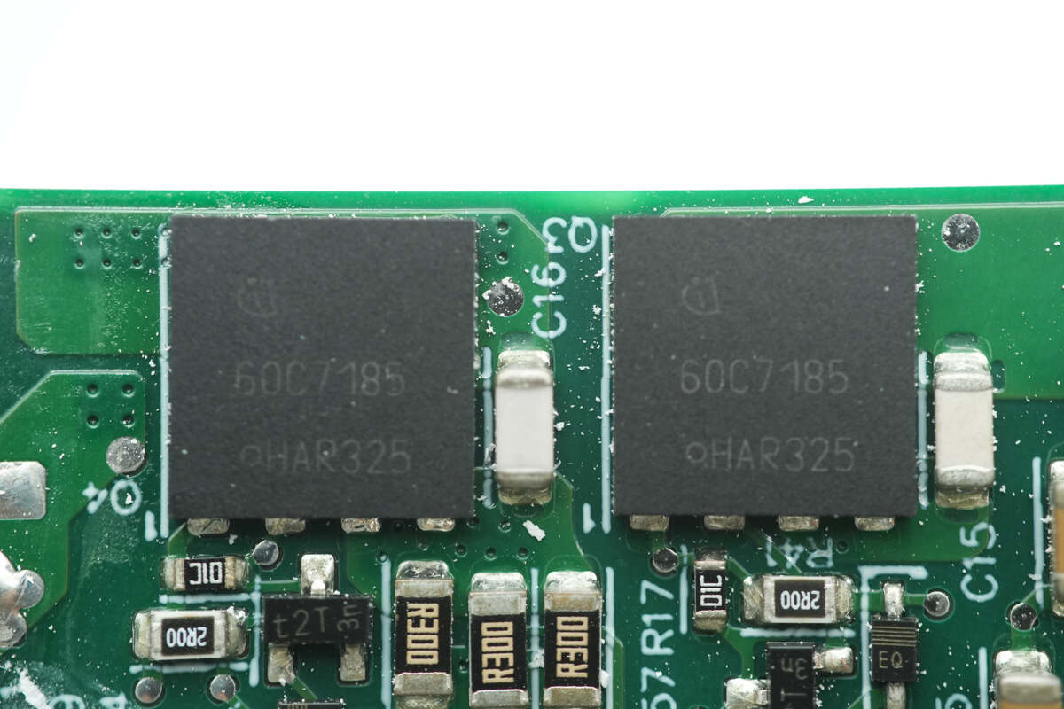
The primary MOSFETs are from Infineon, marked with 60C7185, model IPL60R185C7. They are NMOS devices with a voltage rating of 650V and an on-resistance of 185mΩ, housed in a ThinPAK 8×8 package.
A close-up of three parallel-connected resonant capacitors.
A close-up of the other two resonant capacitors.
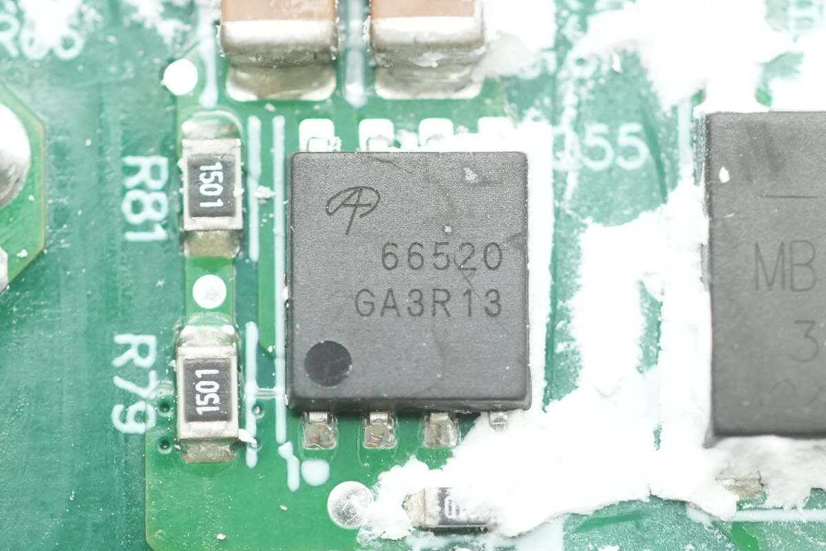
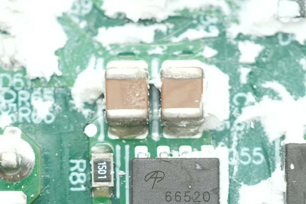
The MOSFET used to control the resonant capacitor is from AOS, model AONS66520. It is an N-channel MOSFET with a voltage rating of 150V, an on-resistance of 9.5mΩ, and comes in a DFN 5x6 package.
Here is the information about AOS AONS66520.
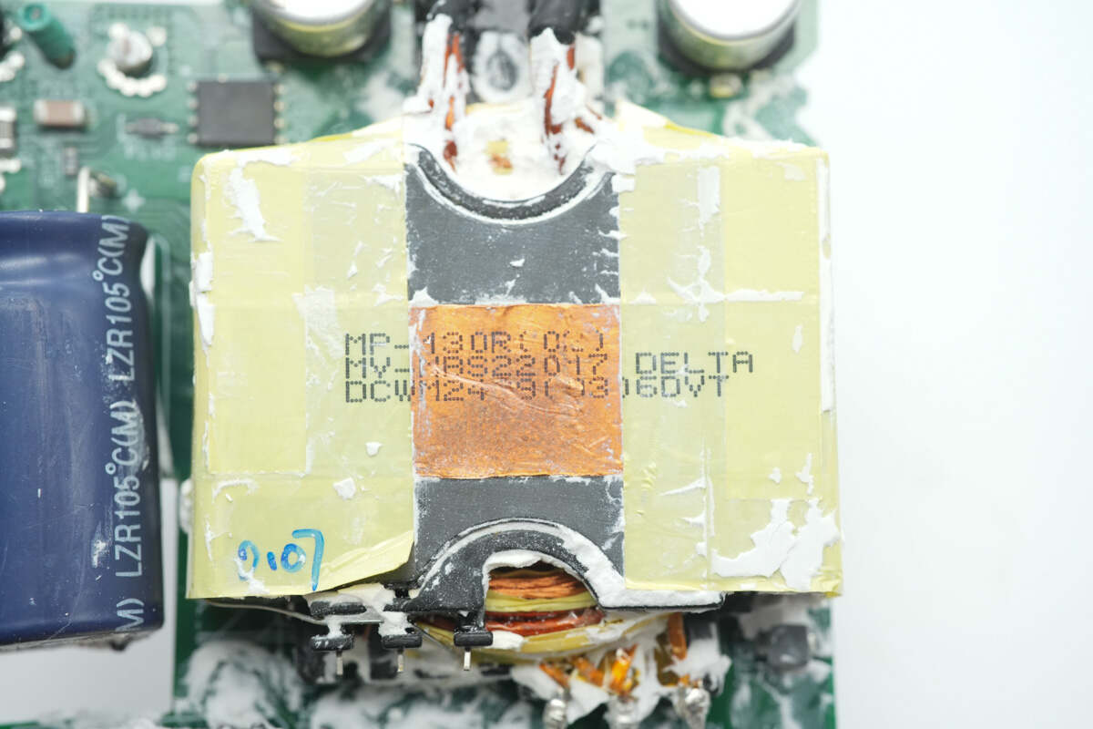
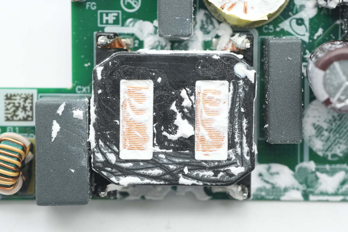
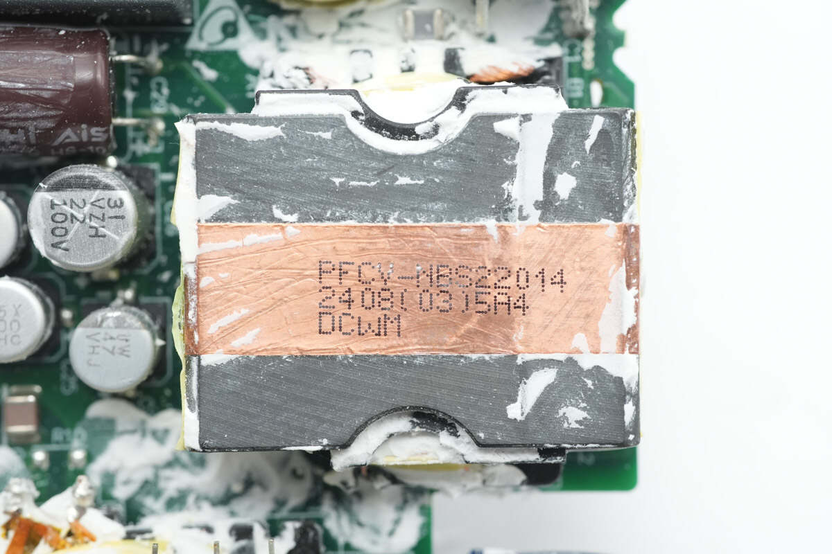
Close-up of the transformer.

The LITEON LTV-1004 optocoupler is used for output voltage feedback, with plastic brackets soldered on both sides for support.

Close-up of another optocoupler, with the same part number LTV-1004.
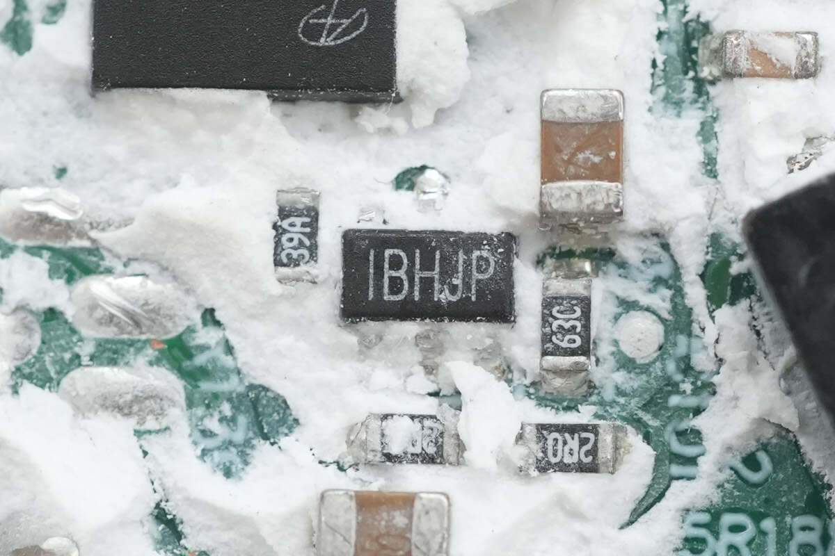
The synchronous rectifier controller, marked with IBHJP, is the MP6908A from MPS. It supports a maximum operating frequency of 600 kHz and multiple working modes, including DCM, CCM, QR, and ACF. The device is suitable for both high-side and low-side applications and features ringing detection to prevent false turn-on. It comes in a TSOT23-6 package.
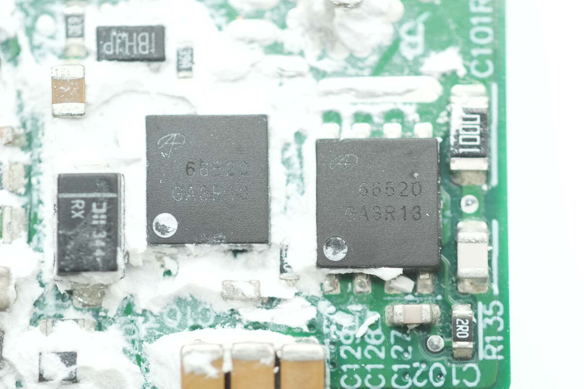
The synchronous rectifiers also use AOS AONS66520.
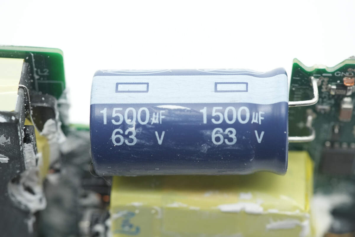
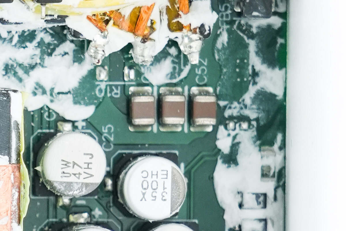
The electrolytic capacitor for output filtering is from LTEC, rated 63V 1500μF.
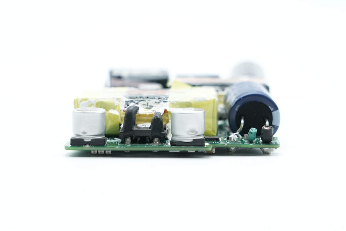
There are two filtering capacitors and a VBUS MOSFET at the output end.
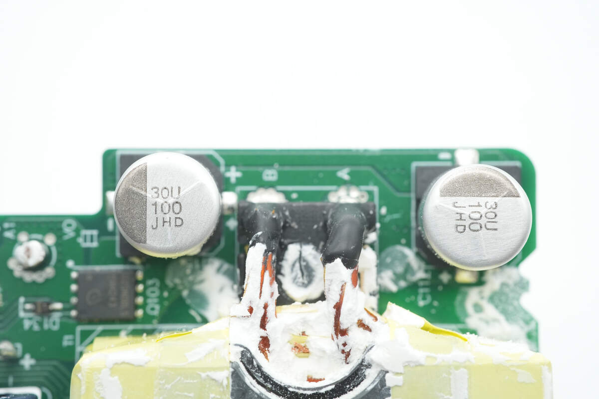
The output filtering capacitors are from NCC, HXD series conductive polymer hybrid aluminum electrolytic capacitors, rated at 63V 100μF.
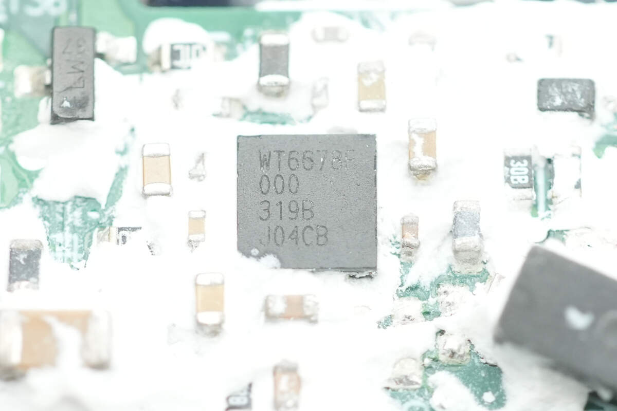
The protocol chip is from Weltrend, model WT6678F, supporting USB PD 3.1 SPR and ERP 48V standards. It integrates PD PHY, USB Type-C detection, voltage and current detectors, an MCU, and drivers. It supports an operating voltage range of 3.3–56V and comes in a QFN16 package.
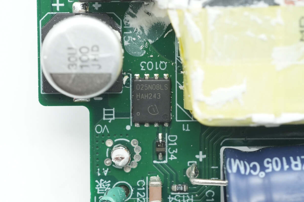
The VBUS MOSFET is from Infineon, model BSC025N08LS5, with an 80V voltage rating and 2.5mΩ on-resistance, packaged in TDSON-8.
Well, those are all components of the Delta 240W PD3.1 USB-C Power Adapter.
Summary of ChargerLAB
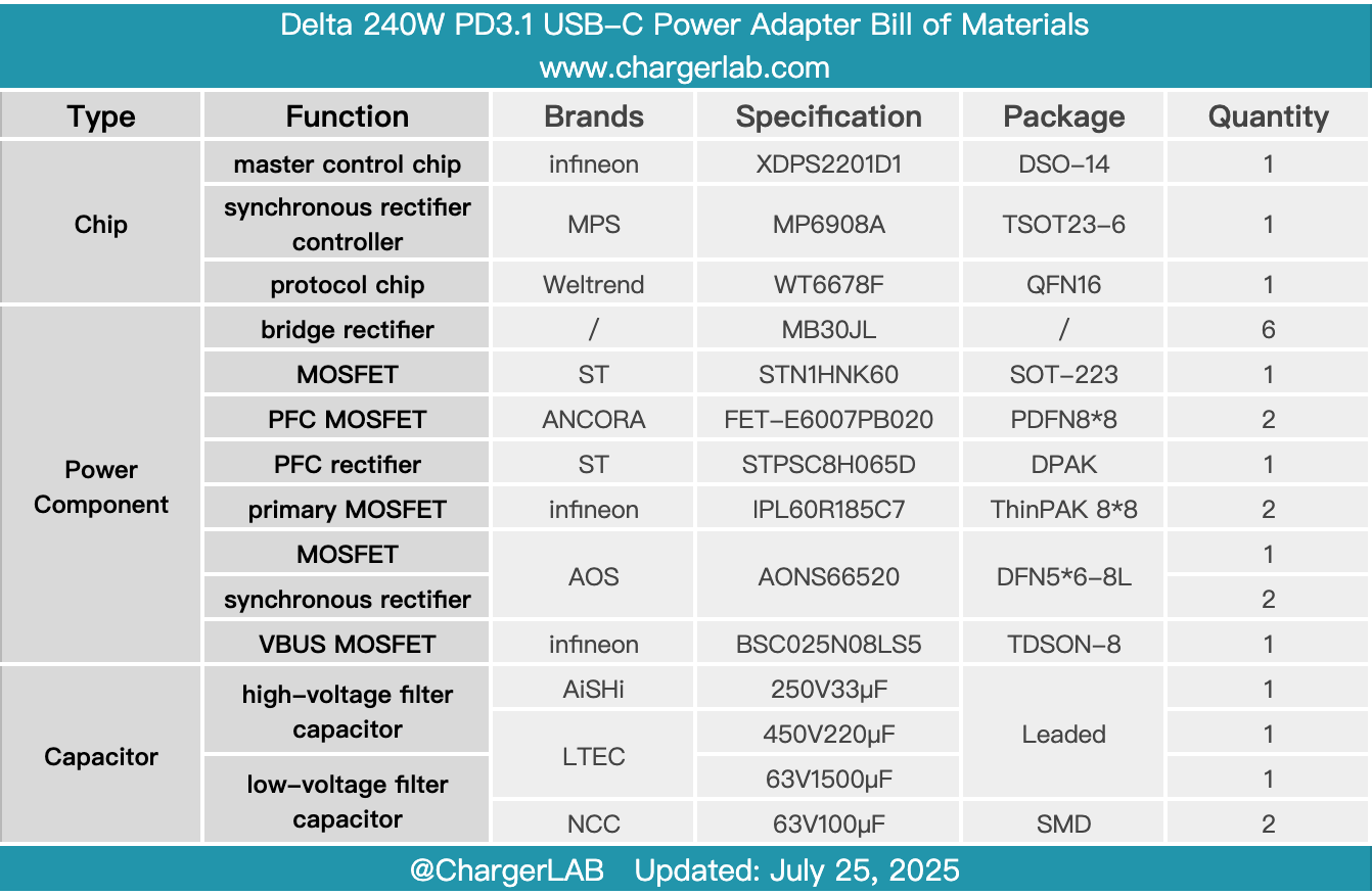
Here is the component list of the Delta 240W PD3.1 USB-C Power Adapter for your convenience.
It continues the traditional power adapter design, comes with a built-in USB-C output cable, and supports PD 3.1 240W output. Its powerful performance is enough to meet the power needs of a wide range of devices.
After taking it apart, we found that it is designed based on a power solution consisting of the Infineon XDPS2201D1 master control chip and the MPS MP6908A synchronous rectifier controller. It uses power devices from well-known manufacturers, including ANCORA FET-E6007PB020 GaN PFC MOSFETs, STMicro STPSC8H065D silicon carbide PFC rectifiers, Infineon IPL60R185C7 primary MOSFETs, and AOS AONS66520 synchronous rectifiers.
The output is controlled by the Weltrend WT6678F protocol chip. The filtering capacitors are also sourced from well-known manufacturers such as LTEC, AiSHi, Lelon, and NCC. The component selection is truly premium. The PCBA module is covered with a heat sink, and the workmanship is excellent.
Related Articles:
1. Teardown of Ford 1760W Portable EV Charger
2. Teardown of Enphase IQ8P 480W Microinverter (IQ8P-72-2-INT)
3. Teardown of Xiaomi 33W 5000mAh 3-in-1 Power Bank (NPB0533)