Introduction
ChargerLAB recently got a magnetic power bank from CUKTECH, with a simple and elegant appearance. It has a USB-C port and a USB-C cable, both support PD 20W fast charging, and it also supports 7.5W wireless output. There are also two indicator lights for wireless charging and wired charging. Next, take its 253W power adapter apart to see its internal components and structure.
Product Appearance
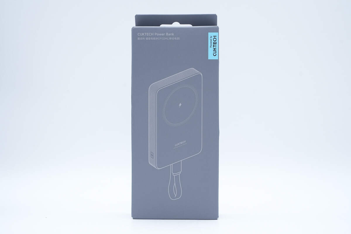
The packaging box adopts CUKTECH's consistent gray tone, and the product appearance outline is printed on the front.
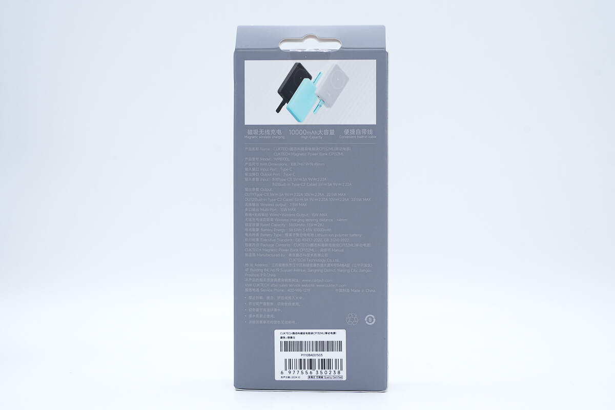
The specs info is printed on the back.

Model: CP132ML
Item Dimensions: 108.7 x 67.9 x 19.45 mm
Input Port: Type-C
Output Port: Type-C
Input:
IN1(Type-C1): 5V3A、9V2.22A
IN2(Built-in Type C2 Cable): 5V3A、9V2.22A
Output:
OUT1(Type-C1): 5V3A、9V2.22A、10W2.25A、22.5W(MAX)
OUT2(Built-in Type C2 Cable): 5V3A、9V2.22A、10W2.25A、22.5W(MAX)
Wireless output: 7.5W MAX
Multi-Port: 15W MAX
Wired+Wireless Output: 15W MAX
Wireless charging sensing distance: ≤4mm
Rated Capacity: 5800mAh(5V2A)
Battery Energy: 36.5Wh 3.65V 10000mAh
Battery Type: Lithium-ion polymer battery

The packaging contains the power bank and some documents.

There is a white sticker on the magnetic panel, which contains instructions for the use of the product.

It has a frosted surface and rounded edges with a delicate touch.

CUKTECH is printed on the upper right corner of the front, and 10000mAh is printed on the lower right corner.
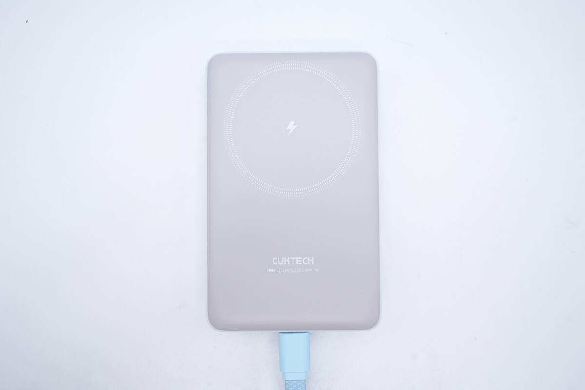
The magnetic panel uses a white ring to indicate the position of the magnet.
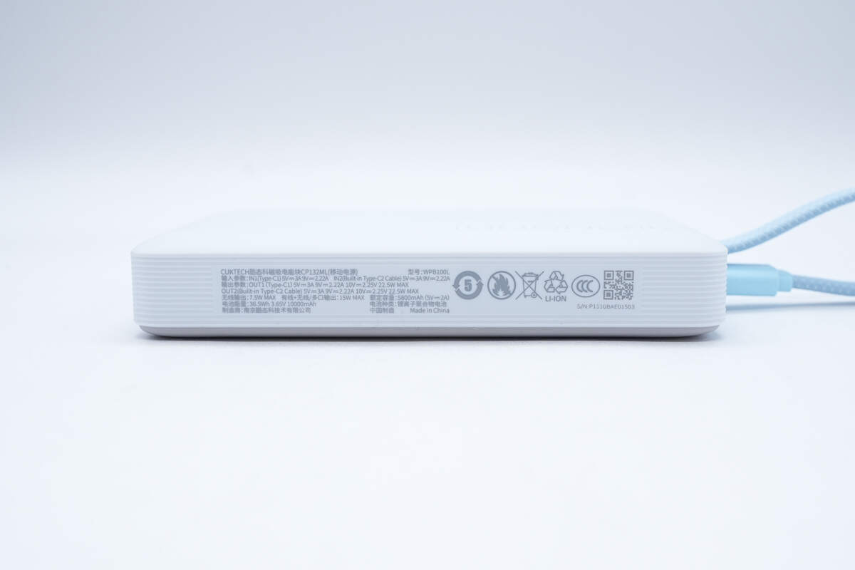
The specs info is also printed on the side.

There are two LED indicator lights on the right side.
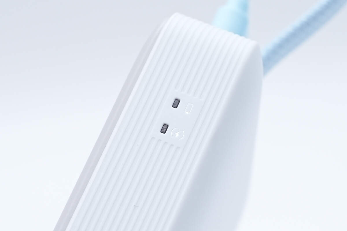
Two are used for wireless and wired indication respectively.
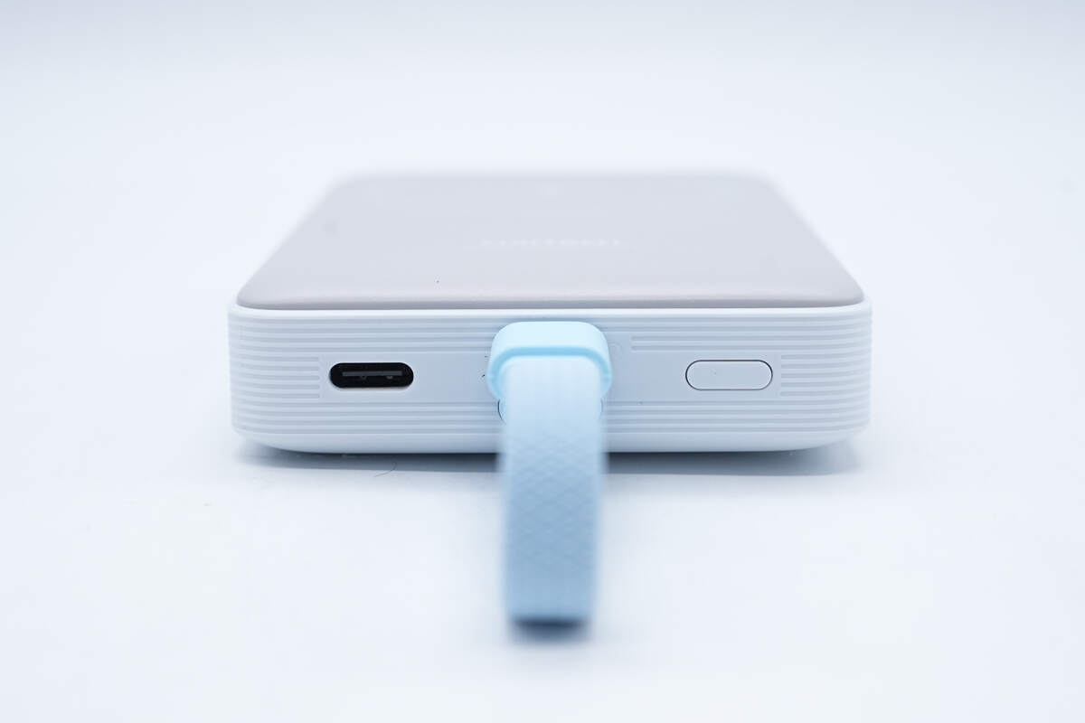
From left to right are the USB-C port, USB-C integrated cable, and the switch button.

The slot of the integrated cable does not have input/output capabilities.
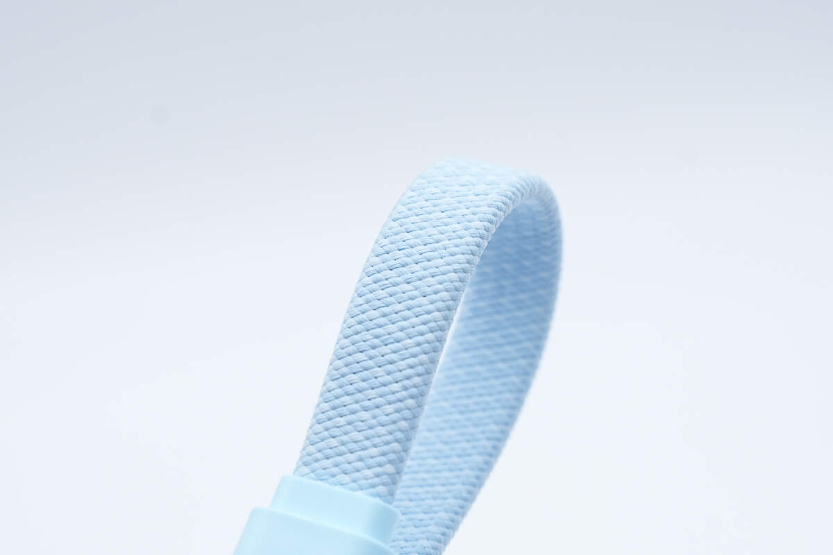
The cable is braided.
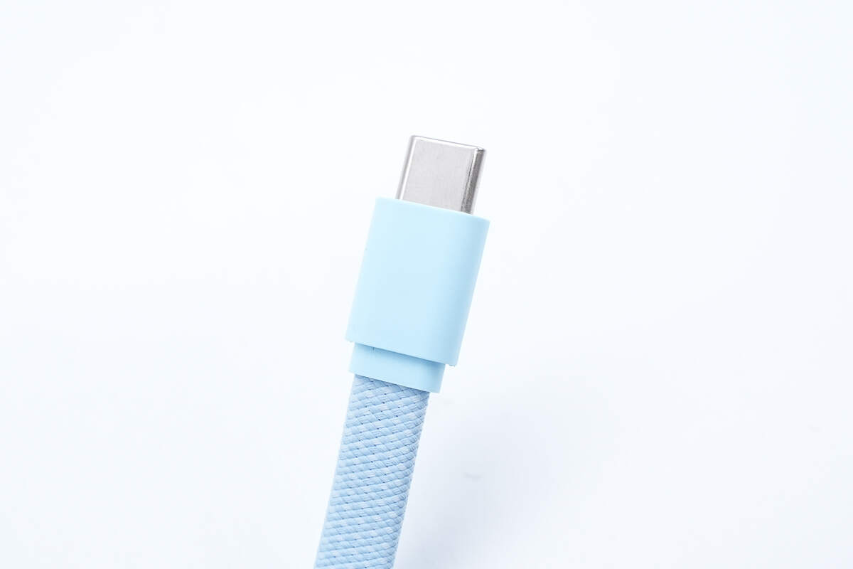
There is no information engraved on the connector.

The length of the cable is about 11 cm (4.33 inches).
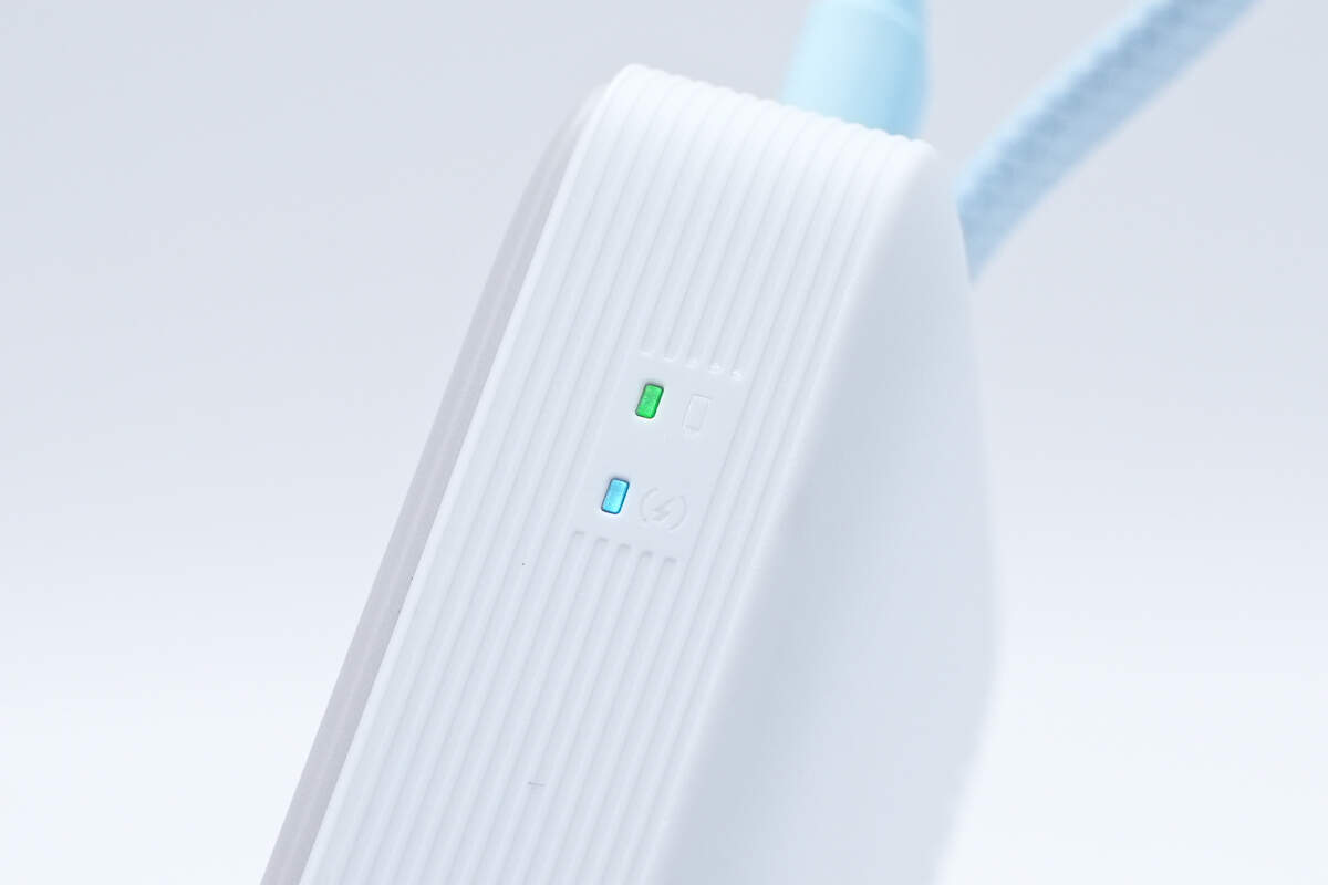
The wireless indicator light is blue and the wired indicator light is green.
When a single device is using both wireless and wired charging, it automatically switches to the faster wired charging mode.

The length of the power bank is about 108.84 mm (4.29 inches).
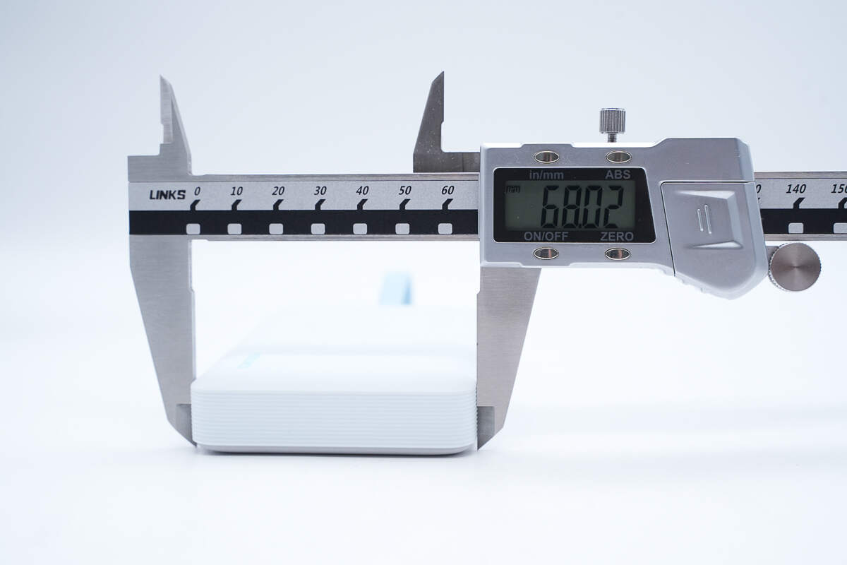
The width is about 68.02 mm (2.68 inches).
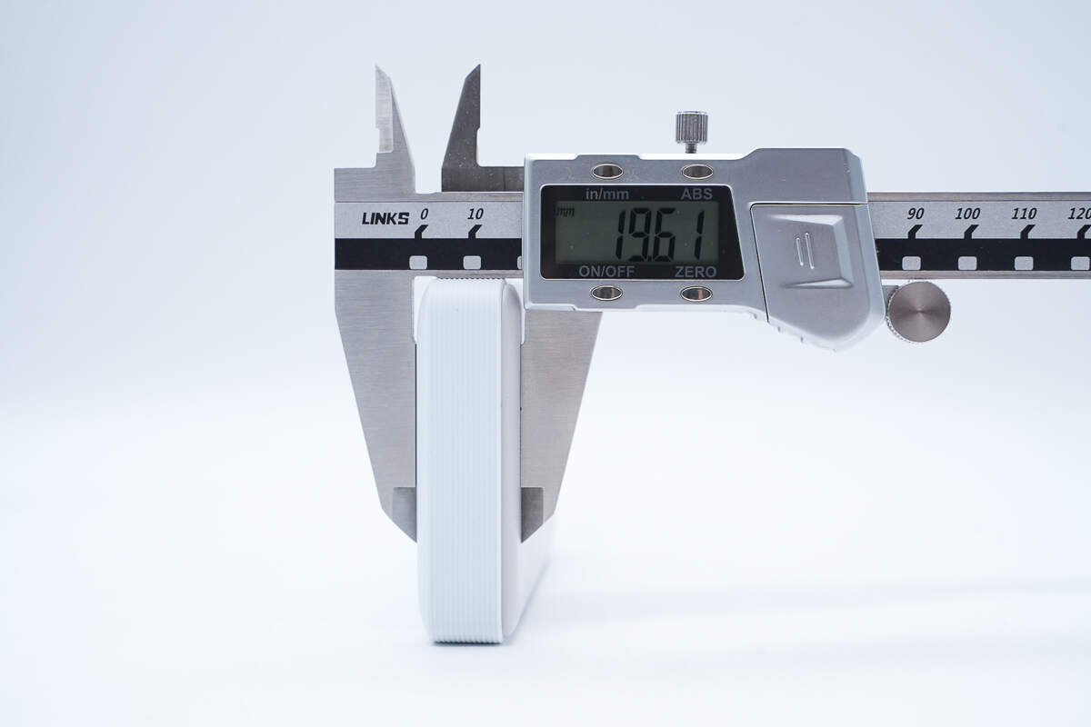
The thickness is about 19.61 mm (0.77 inches).
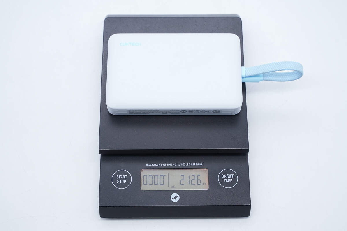
The weight is about 212.6 g (7.5 oz).

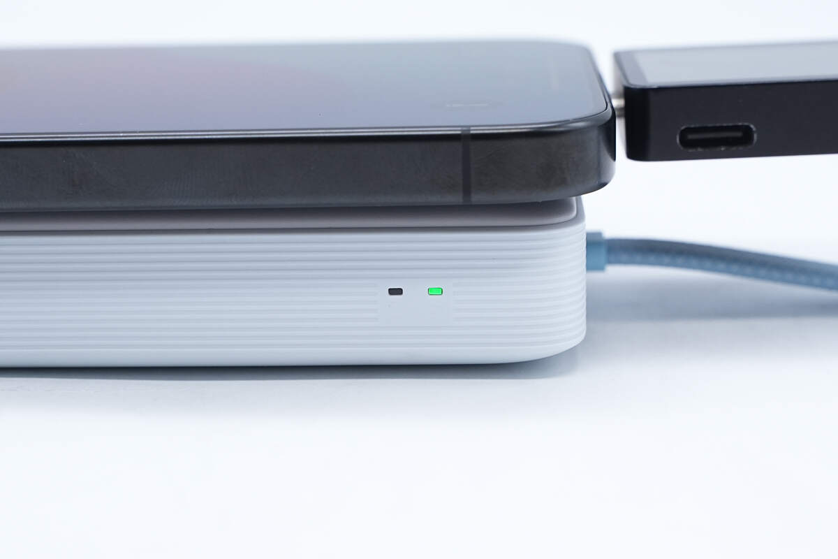
That's how big it is in the hand.
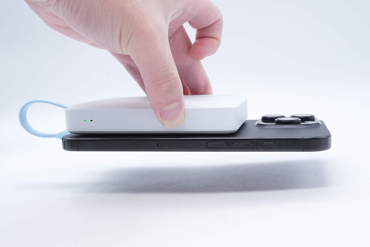
The magnetic force is so strong that the phone won't fall off even if it's upside down.
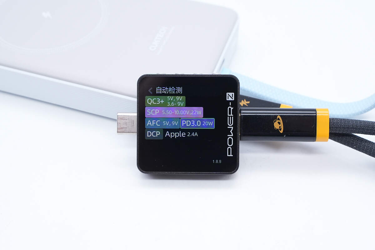
ChargerLAB POWER-Z KM003C shows the USB-C port can support QC3+, SCP, AFC, PD3.0, DCP, and Apple 2.4A charging protocols.

And it has two fixed PDOs of 5V2.4A and 9V2.22A.
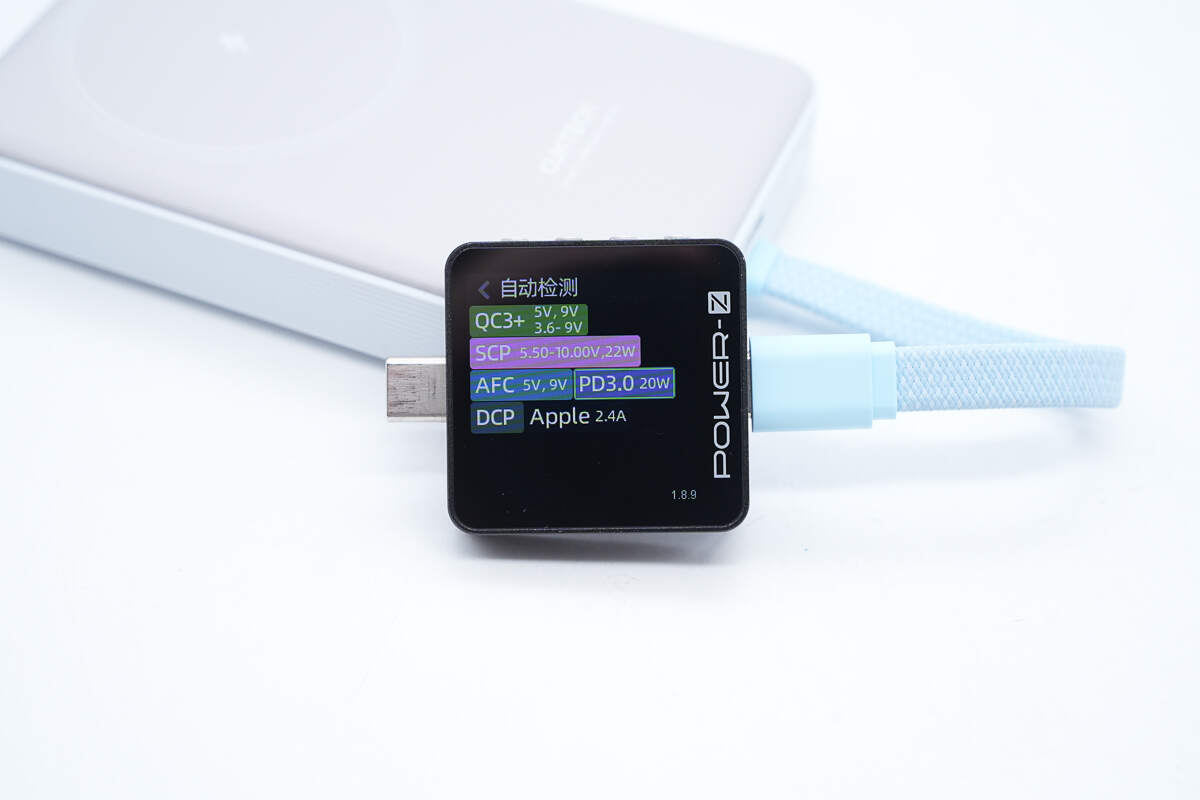
Our tester shows the cable can support QC3+, SCP, AFC, PD3.0, DCP, and Apple 2.4A charging protocols, the same as the USB-C port.

So as the PDOs.
Teardown
Next, let's take it apart to see its internal components and structure.

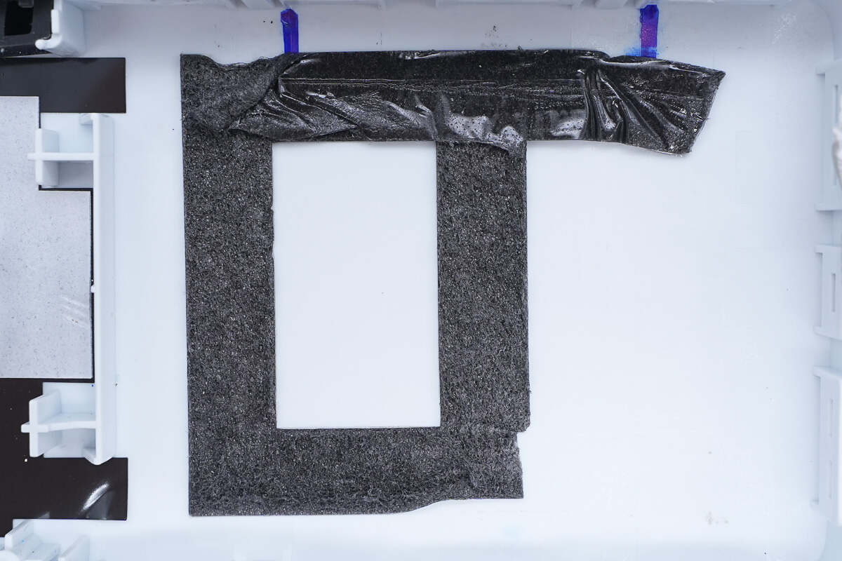
First, pry along the gap to open the cover.

There are magnets embedded under the cover. There is a ring-shaped metal sheet on the upper layer of the ring-shaped magnet ring for fixing.

There is a layer of sticker on the contact surface with the PCBA module.
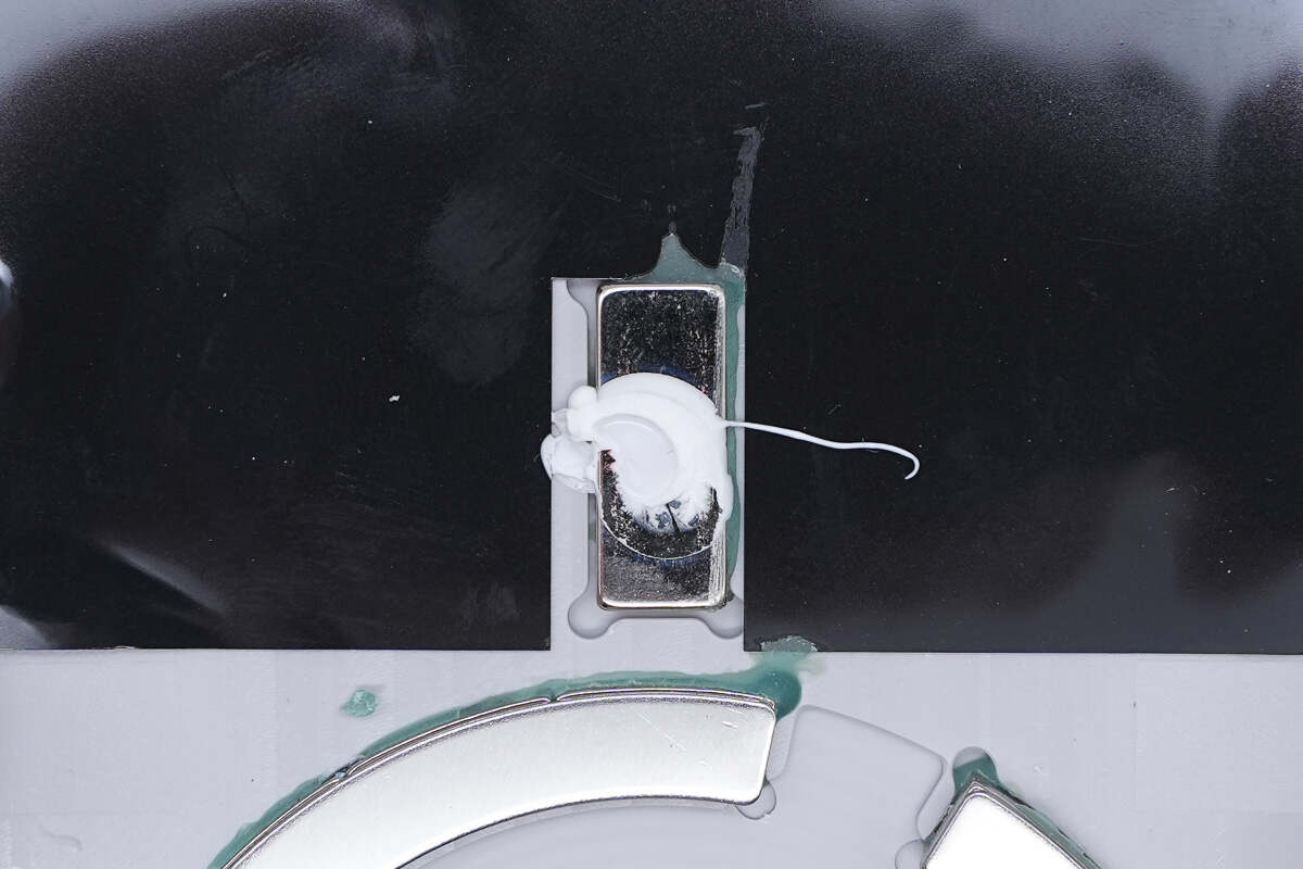
This long strip of magnet is reinforced with glue.
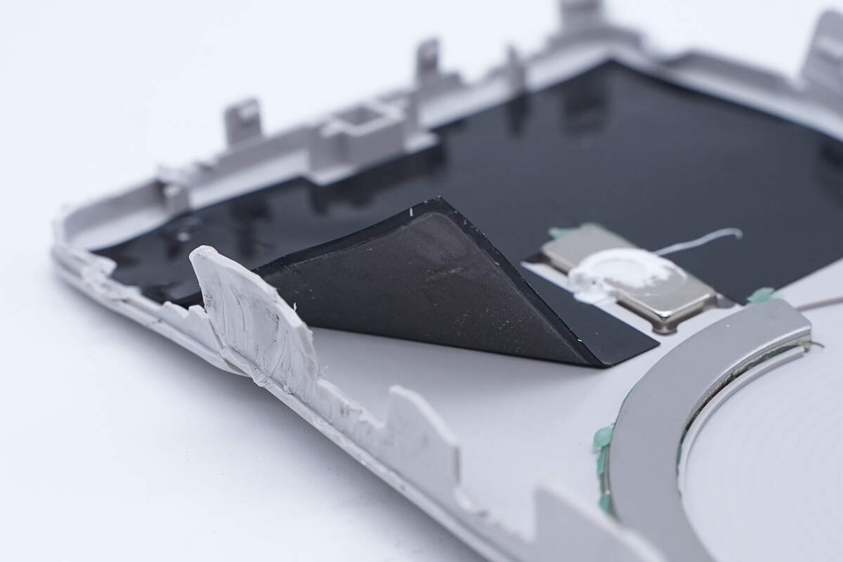
Opening the sticker, we found that it uses a composite material of plastic and graphite, which can both insulate and help dissipate heat.

Remove the ring-shaped metal sheet and you will see that the magnets inside are glued together.
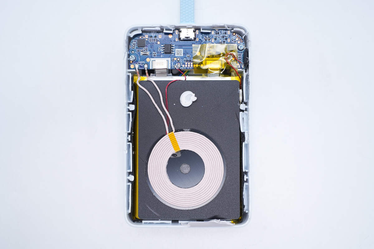
Let’s take a look at the internal structure on the other side.

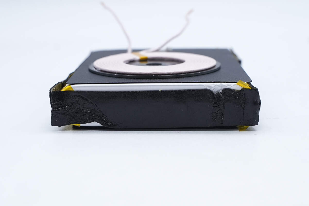
The wireless charging coil is wound with yarn-wrapped wire and attached to the top of the battery cell.
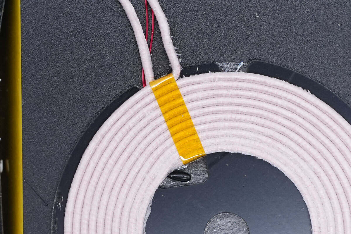
The coil is tied tightly with high-temperature tape to prevent it from falling apart. A thermistor is fixed between the magnetic isolation sheet and the coil for temperature monitoring.
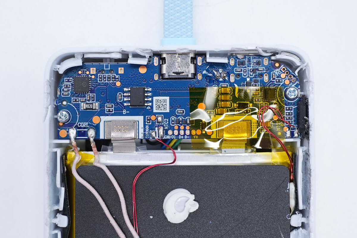
Above the battery pack is the PCBA module.
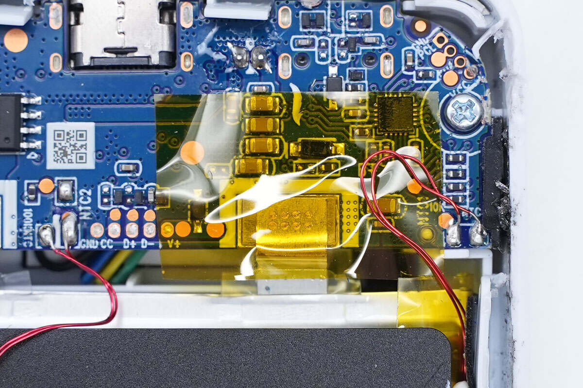
This solder joint of the battery is covered with high-temperature tape for insulation.

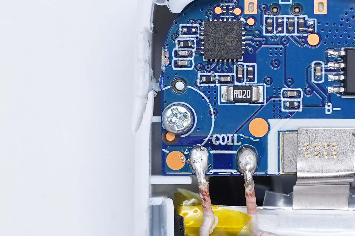
This is another solder joint.
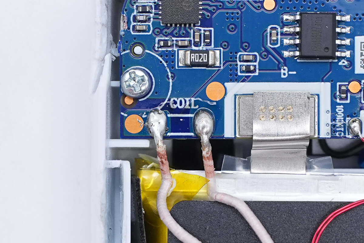
This is the soldering point of the coil on the PCBA module.
The PCBA module is fixed with screws.
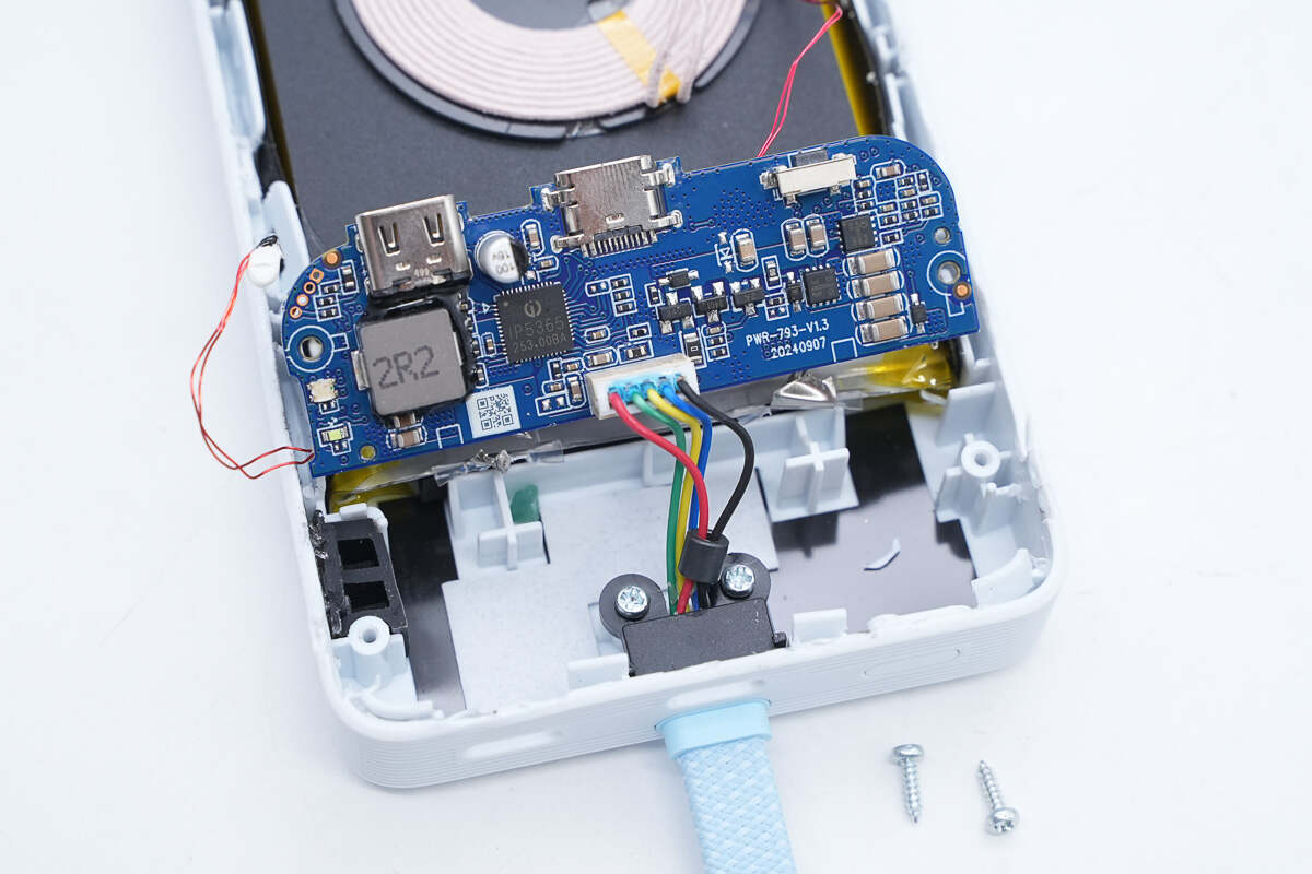
Turn the PCBA module over and look at the structure on the other side.

This is the socket for the integrated cable.
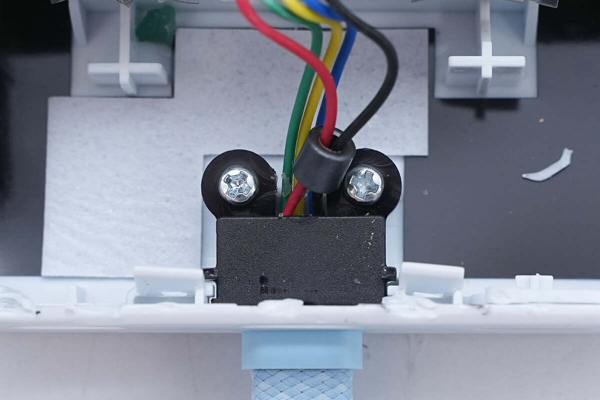
The other side is secured with screws.
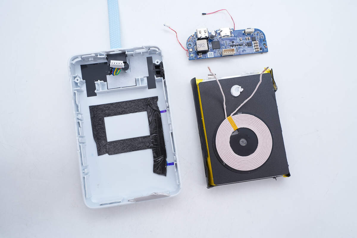
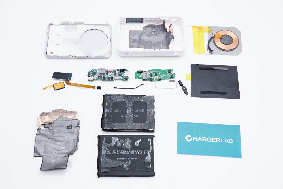
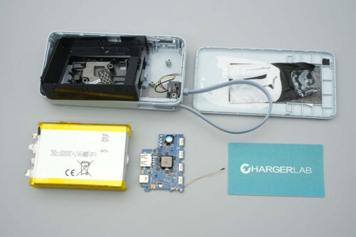
Remove the PCBA module and battery pack from the housing.
The contact surface with the battery cell is covered with foam for cushioning protection.

An overview of the battery pack and coil.
The battery pack is also protected by foam cushioning.
There is also foam on the bottom and a layer of double-sided tape on the outside.
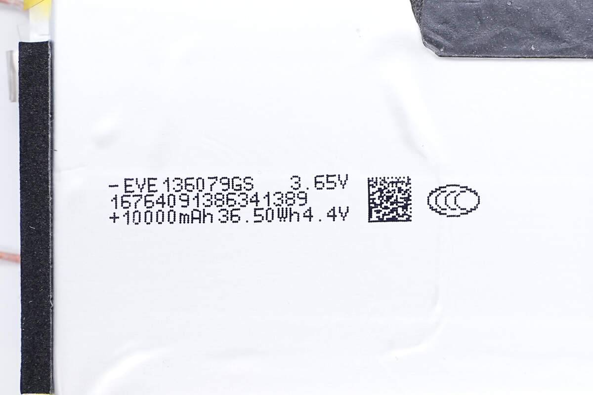
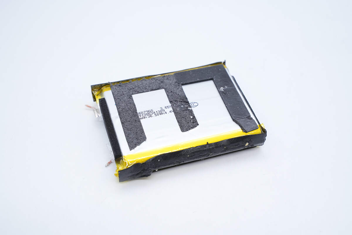
The battery cell is from EVE. Nominal voltage 3.65V, charging limit voltage 4.4V, nominal capacity 10000mAh, energy 36.5Wh. Model is 136079GS.
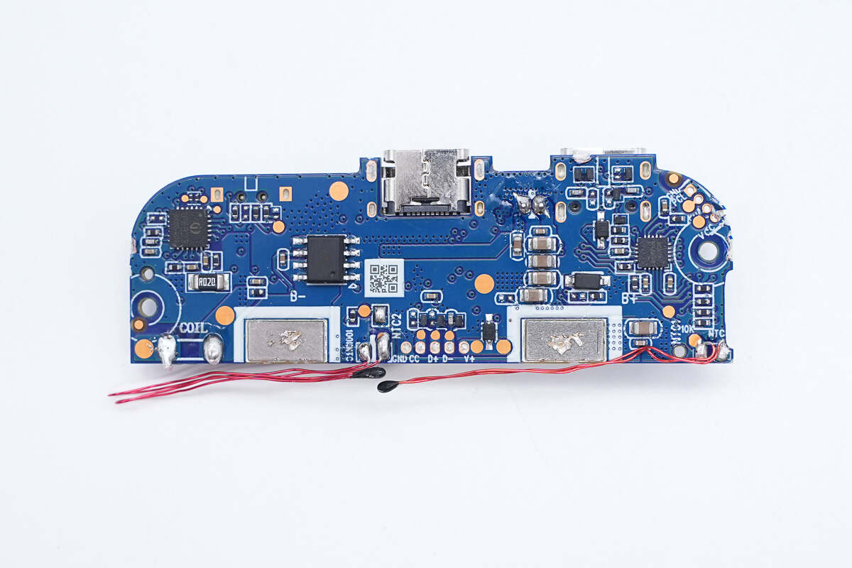
The front of the PCBA module has a wireless charging master control chip, a battery protection chip, a USB-C female connector, an MCU, and two thermistors.

The back of the PCBA module has an alloy inductor, SOC, USB-C cable socket, VBUS MOSFET, two wireless charging MOSFETs, and a series of resonant capacitors.
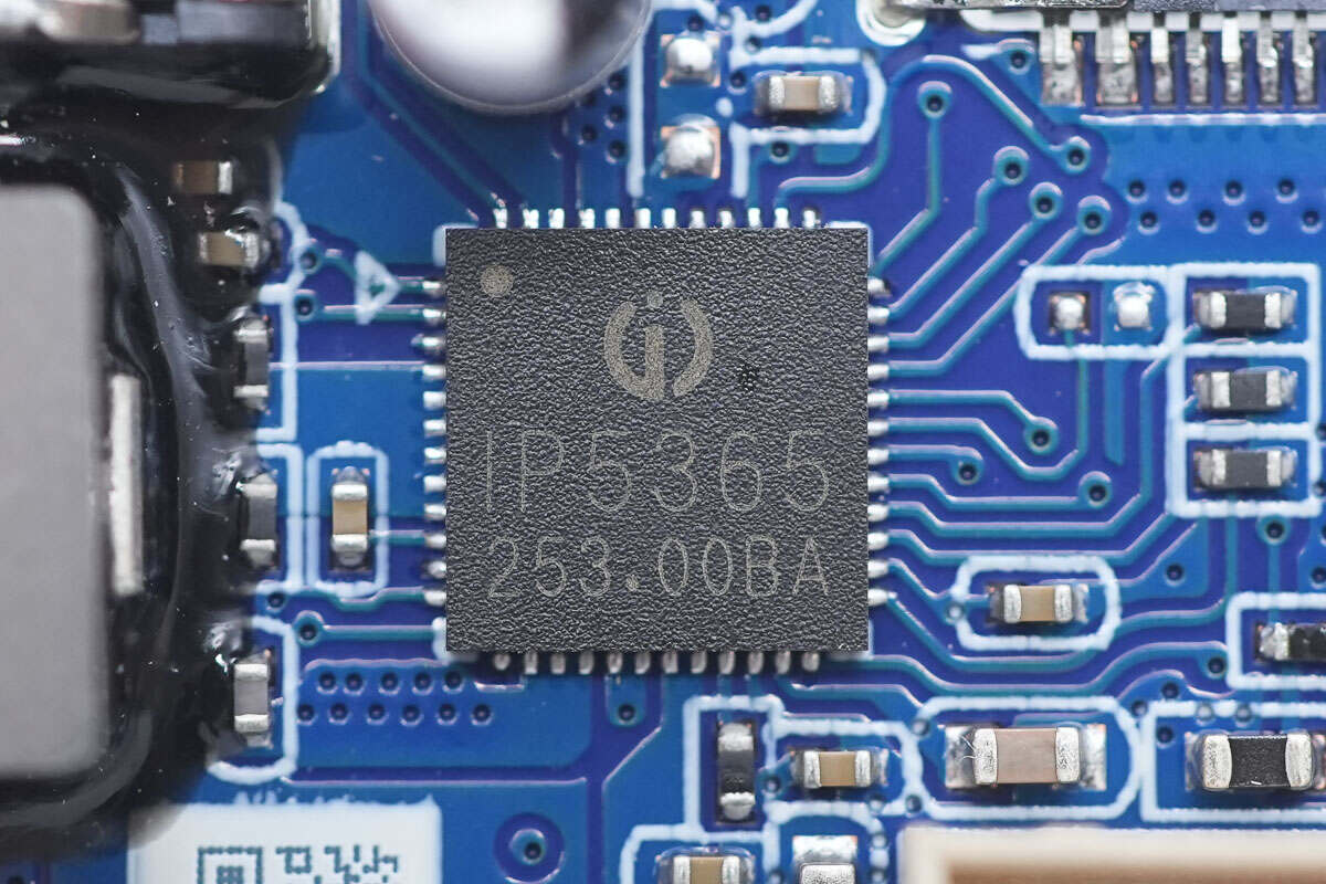
The SoC is from INJOINIC. It supports PD3.0, PPS, UFCS, AFC, and SCP fast charging protocols, and integrates Lightning input communication. It supports 18W fast charging, the battery charging current can reach 5A, and supports 4.2, 4.3, 4.35, and 4.4V battery applications. The chip has built-in MOSFET and VBUS MOSFET, internal integrated 14-bit ADC, supports 1-4 LED power display, 88 or 188 digital tube power display, supports automatic power on and off, integrated input overvoltage, under-voltage protection, output overcurrent, overvoltage, short circuit protection, battery overcharge, over-discharge and overcurrent protection, built-in overheat protection, and supports external NTC for battery temperature protection. Model is IP5365.

Here is the information about INJOINIC IP5365.
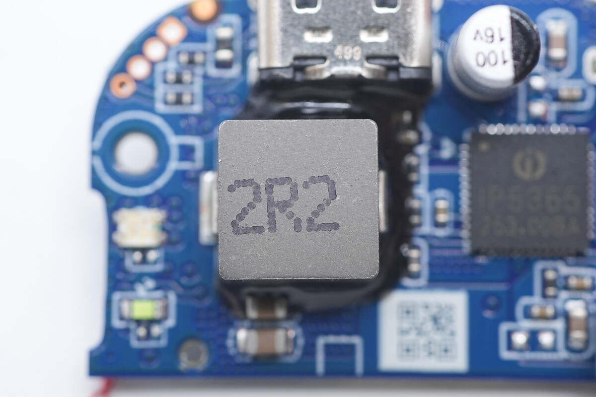
The alloy inductor is reinforced with glue. 2.2μF.
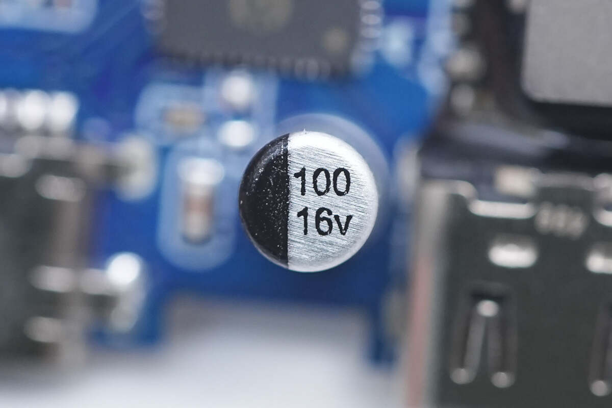
The capacitors are soldered through the vias. 100μF 16V.
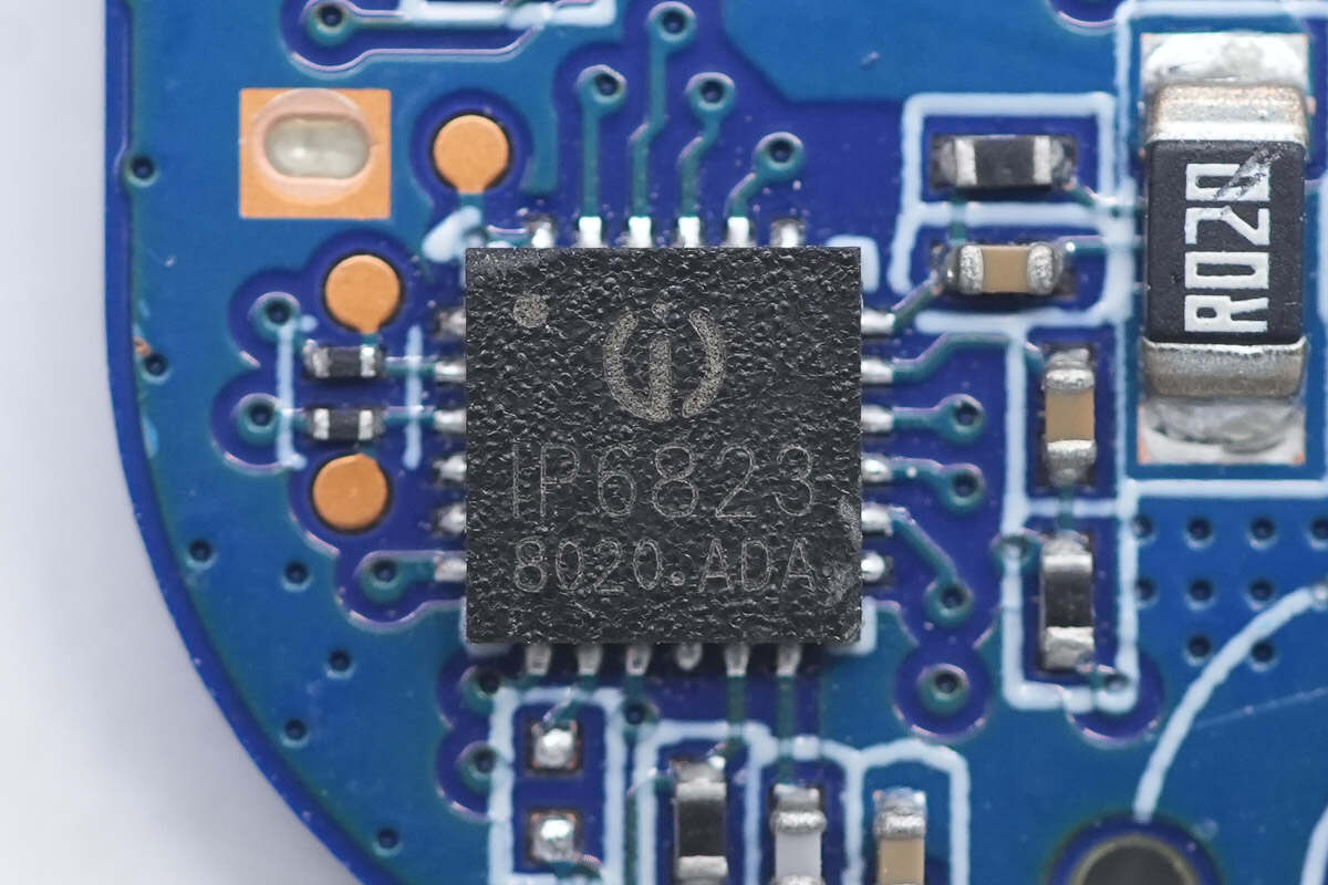
The wireless charging master control chip is from INJOINIC and adopts QFN24 package. It is a highly integrated wireless charging transmitter control chip that complies with the WPC qi standard. It integrates an H-bridge driver module and an ASK communication demodulation module. Model is IP6823.
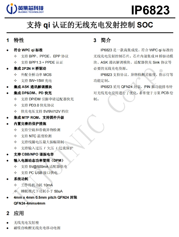
Here is the information about INJOINIC IP6823.
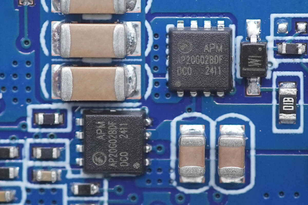
These two wireless charging MOSFETs are from APM and adopt the PDFN3*3-8L package. It has a withstand voltage of 20V. Model is AP20G02BDF.

There are NPO resonant capacitors.

The MCU marked with M320F3V6 is from CHIPSEA and adopts the QFN20 package. It has built-in 8K×16-bit Flash and 488 bytes of SRAM, covering a variety of products with 16 to 20 pins. It provides standard communication interfaces (including I2C and UART), equipped with 12-bit ADC, CVC, and timer functions. Its operating temperature range is -40℃~85℃, and the operating voltage is 1.8V5.5V. Model is CS8M320.

Here is the information about CHIPSEA CS8M320.
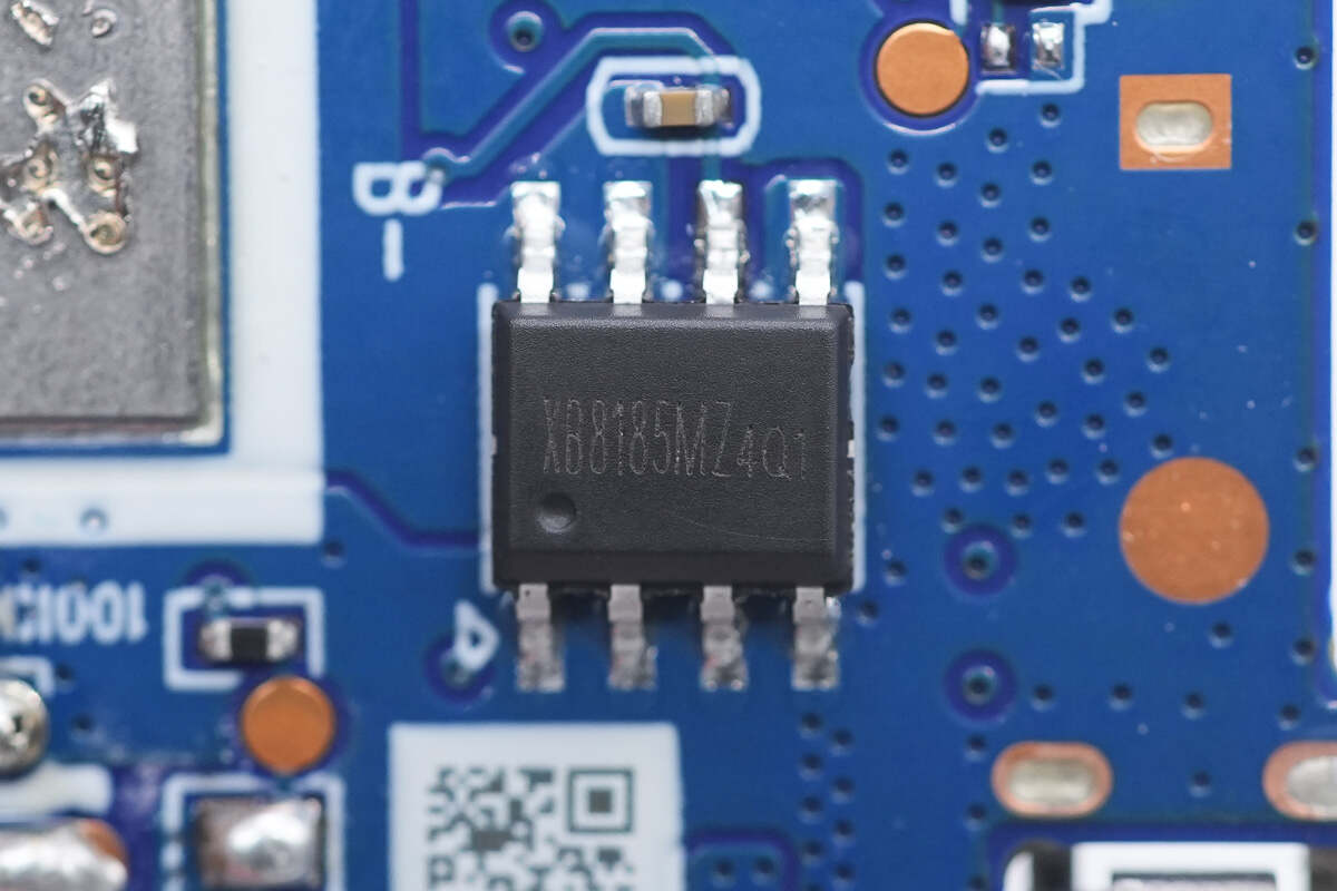
The battery protection chip marked with XB8185MZ is from Xysemi and adopts the SOP8 package.

The USB-C socket has a black plastic sheet.

This is the SMD switch button.

This is the socket of the integrated cable.

There are indicator beads.

The NTC thermistor is used to monitor the battery pack temperature and provide over-temperature protection.
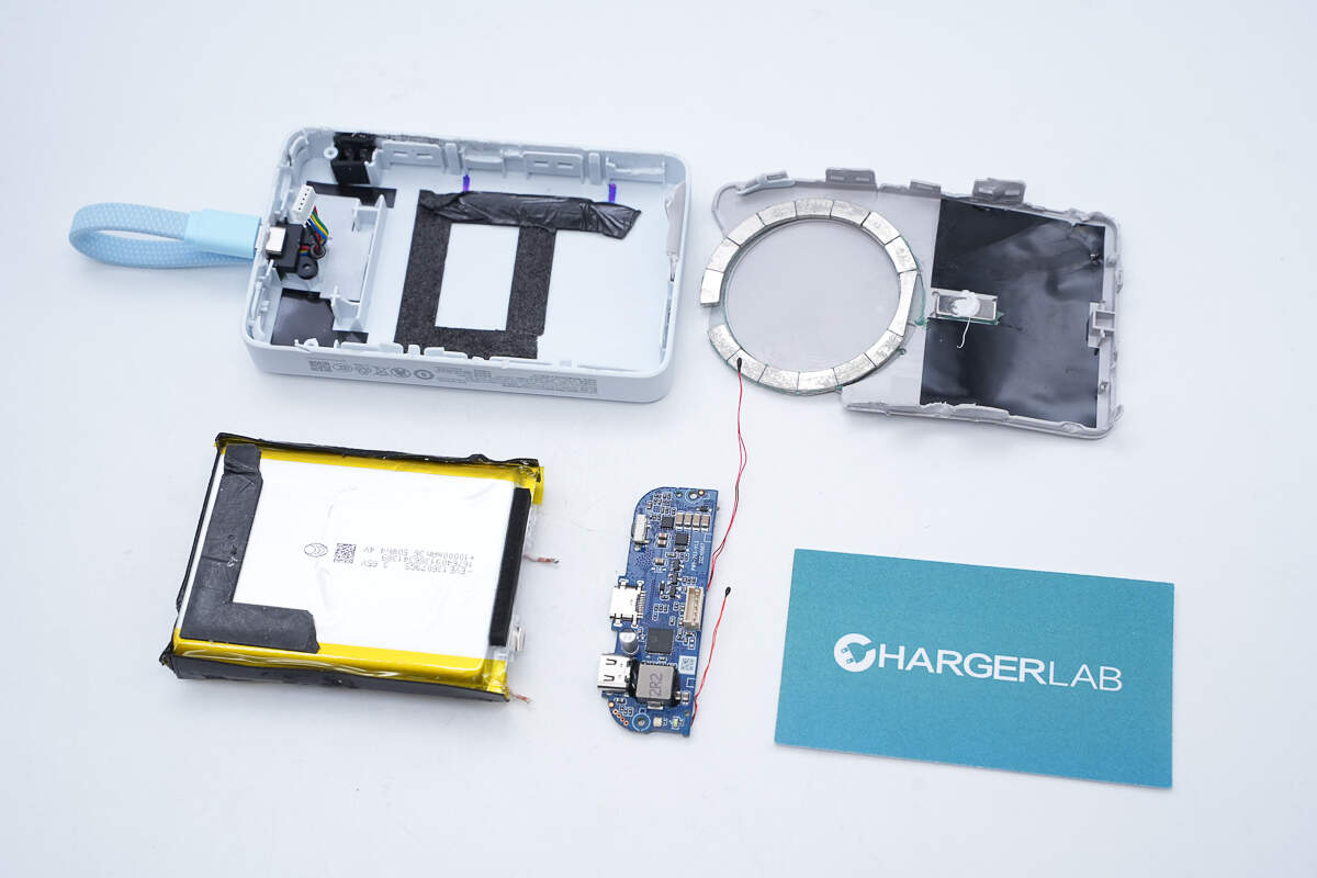
Well, those are all components of the CUKTECH 10000mAh Magnetic Power Bank.
Summary of ChargerLAB

Here is the component list of the CUKTECH 10000mAh Magnetic Power Bank for your convenience.
It has a battery capacity of 10000mAh, equipped with a USB-C port and a USB-C cable, both of which support PD 20W fast charging. The wireless charging module supports a maximum output of 7.5W.
After taking it apart, we found that graphite stickers are attached around the battery pack and PCBA module for heat dissipation, and two thermistors are used to monitor the temperature of the battery pack and PCBA module respectively. Its internal structure is stable and reliable, and the space utilization is compact and reasonable.
Related Articles:
1. Teardown of OPPO 5000mAh Slim Magnetic Power Bank (MPBV01)
2. Teardown of Xiaomi 5000mAh Ultra-thin Power Bank (PB0520MI)
3. 5000mAh | Teardown of Tesla Wireless Portable Charger (TSL02)