Introduction
CUKTECH has launched the 10 Mini GaN Charger. This charger is very compact, measuring 44.5 × 39 × 60 mm, and features a sleek, attractive design. It features foldable plugs for easy portability. The charger is equipped with two USB-C ports and one USB-A port. Both USB-C ports support Xiaomi’s 120W Surge fast charging and 100W PD, while the USB-A port supports 33W UFCS fast charging.
It offers versatile multi-port output options, allowing you to quickly charge laptops, tablets, and smartphones at the same time. Next, let’s take it apart to see its internal components and structure.
Product Appearance

The packaging box front displays the product name, an image of the charger, “Powered by CUKTECH,” and “GaN.”

The back displays usage scenarios, key features, and specifications.

The package includes the charger, cable, and some documents.

The USB-C cable has a matte-finish connector housing, with “CUKTECH” and “6A” engraved on each end.

The length of the cable is about 101 cm (39.76 inches).

ChargerLAB POWER-Z KM003C shows that the cable has an E-Marker chip, supporting power delivery up to 50V/5A and data transfer at USB 2.0 speed.

The casing features a gray and black contrast design, compact and refined.

The front is printed with "CUKTECH," "120W GaN Adapter," and the number "10."

The input-side casing is printed with the specification.

Model: AD1203P
Input 1: 100-240V\~50/60Hz 1.7A
Output 1:
C1/C2: 5V⎓3A, 9V⎓3A, 11V⎓6.1A, 12V⎓3A, 15V⎓3A, 20V⎓5A (100W Max)
A: 5V⎓3A, 9V⎓2A, 12V⎓1.5A, 11V⎓3A (33W Max)
C1 + C2: 67W + 33W Max
C1/C2 + A: 67W + 22.5W Max
C1 + C2 + A: 45W + 33W + 18W Max
Input 2: 200-240V\~50/60Hz 1.7A
Output 2:
C1/C2: 20V⎓6A (120W Max)
C1 + C2: 67W + 55W Max
C1/C2 + A: 90W + 22.5W Max
C1 + C2 + A: 45W + 45W + 22.5W Max
Certified by CCC.

Equipped with foldable prongs.

The top features two USB-C ports and one USB-A port.

The length is about 60.06 mm (2.36 inches).

The width is about 39.33 mm (1.55 inches).

The thickness is about 44.88 mm (1.77 inches).

That's how big it is in the hand.

The weight is about 182 g (6.42 oz).

ChargerLAB POWER-Z KM003C shows that the USB-C1 supports PD3.0, DCP, and Apple 2.4A charging protocols, as well as Xiaomi’s proprietary 120W protocol.

And it has five fixed PDOs of 5V3A, 9V3A, 12V3A, 15V3A, and 20V5A, as well as two Xiaomi proprietary voltage ranges of 5-11V6A and 5-20V6A.

The USB-C2 supports UFCS, PD3.0, DCP, and Apple 2.4A charging protocols, as well as Xiaomi’s proprietary 120W protocol.

And it has five fixed PDOs of 5V3A, 9V3A, 12V3A, 15V3A, and 20V5A, as well as two Xiaomi proprietary voltage ranges of 5-11V6A and 5-20V6A.

The USB-A supports UFCS, FCP, SCP, AFC, QC3.0, DCP, and Apple 2.4A charging protocols.

Using USB-C1 to charge the Redmi K80 Pro successfully activated Xiaomi’s 120W Surge fast charging.

When the charging power stabilized, the power was about 93.08 W.
Teardown
Next, let's take it apart to see its internal components and structure.

Cut open the casing to remove the PCBA module.

The PCBA module is connected to the prongs by wires.

The length of the PCBA module is about 54.99 mm (2.16 inches).

The width is about 40.72 mm (1.6 inches).

The thickness is about 34.79 mm (1.37 inches).

The PCBA module is potted and covered with heatsinks.

After removing the heatsinks, Mylar sheets and insulating tape are found on the inner sides.

The PCBA module features a planar transformer design, with small PCBs on both the input and output ends. Components are tightly stacked, and a plastic casing separates the transformer from the capacitors.

On the back side, there are components including a PFC controller, PFC MOSFET, PFC rectifier, master control chip, primary MOSFET, optocouplers, and an SMD Y capacitor.

A delay fuse is installed on the small PCB at the input side.

After removing the small PCB, the front side features an NTC thermistor, common mode choke, safety X2 capacitor, and bridge rectifiers.

On the other side, there is a film filter capacitor.

The delay fuse is from Betterfuse, part number 936, rated at 3.15A 250V.

The NTC thermistor is used to suppress inrush current during power-up.

The common mode choke is used to filter out EMI interference; it is wound with two wires and insulated with a heat-shrink tube.

The safety X2 capacitor is sourced from Surong. 0.22 μF.

The two bridge rectifiers are from Pingwei, model TMBFR310, rated at 3A 1000V, and use the TMBF package.

The CBB21 film filter capacitor is also from Surong, rated at 1μF 450V.

On this side of the mainboard, there is another film filter capacitor and a PFC boost inductor.

The other Surong CBB21 film filter capacitor is rated at 1.2μF 450V.

The filter inductor is insulated with heat-shrink tubing and mounted on a bakelite base.

The PFC controller is from TI, marked “805C,” model UCC28056. It operates in critical conduction mode and features ultra-low no-load power consumption.

The PFC MOSFET is from TI, model LMG3624. It’s a 650V, 170mΩ GaN FET designed for switch-mode power supply applications. The LMG3624 integrates the power FET and gate driver within an 8mm × 5.3mm QFN package, simplifying the design and reducing component count.

Close-up of the PFC boost inductor.

The PFC rectifier is from Pingwei, model PBMUR5JE. It is an ultra-fast recovery diode rated at 5A 600V, featuring low forward voltage drop and high surge current capability, housed in a PS-277B package.

The two high-voltage filter electrolytic capacitors are from Koshin, each rated at 420V 33μF.

On the other side, there is a planar transformer module, insulated with a plastic casing for isolation.

After removing the small PCB, the left side reveals a synchronous rectifier controller and a synchronous rectifier. The planar transformer core is wrapped in copper foil and grounded.

A label on the top of the transformer core reads "TEC25006" and "CUK."

On the other side, there are a resonant capacitor and a solid capacitor on both sides.

After breaking the core, the internal racetrack-shaped coil of the planar transformer is revealed.

The AHB controller is from JOULWATT, model JW1556. It is an asymmetric half-bridge flyback controller housed in a QFN 4x4-20 package, designed for offline flyback converter applications. It integrates a power boost converter with an input voltage range of 2.5–38V and operates at up to 1.5MHz, supporting fast charging applications from 65W to 300W.
Under heavy loads, the JOULWATT JW1556 operates in ZVS (Zero Voltage Switching) mode with Adaptive ZVS switching to optimize efficiency. Under light loads, it switches to DCM (Discontinuous Conduction Mode) and provides dual output control for both the main power switch and auxiliary switch. Additional features include high-voltage startup, X capacitor discharge, burst mode control, and adjustable line compensation.

Here is the information about JOULWATT JW1556.

The primary MOSFET is also from TI, model LMG2640. It is a 650V GaN power field-effect transistor half-bridge device designed specifically for switching power supply applications. This device integrates half-bridge power FETs, gate drivers, a bootstrap diode, and a high-side gate driver level shifter within a 9mm × 7mm QFN package, significantly simplifying design, reducing component count, and saving PCB space.

The resonant capacitor is rated at 0.27μF 250V.

The SMD Y capacitor is from TRX. Its compact size and light weight make it ideal for high-density power products like GaN fast chargers. The part number is TMY1471K.

The CT 1018 optocoupler is used for output voltage feedback.

Close-up of the other CT 1018 optocoupler.

The synchronous rectifier controller is from JOULWATT, marked "JWRU," model JW7726H. It supports ACF, AHB, DCM, QR, and CCM flyback operation modes, and can be used for both high-side and low-side applications. It supports direct power supply from the output voltage, features ultra-low quiescent current, and offers fast driving capability for CCM mode operation.

Here is the information about JOULWATT JW7726H.

The synchronous rectifier is from Vergiga, model VS18208GPM. It is an NMOS device rated for 100V with an on-resistance of 3.8mΩ, housed in a PDFN 5×6 package.

Here is the information about Vergiga VS18208GPM.

The solid capacitor for output filtering is from Koshin. 25V 100μF.

All three USB interface sockets are soldered onto the small PCB.

The other solid capacitor for output filtering is also from Koshin, rated at 25V 680μF.

The two small PCBs with the USB-C sockets share an identical design. On the front side, there is a buck inductor and a solid capacitor. On the back side, there is a synchronous buck controller, synchronous buck MOSFETs, a protocol chip, and an output VBUS MOSFET.

The synchronous buck controller used is the Injoinic IP6550. It supports up to 36V input and features a built-in NMOS driver, using two external MOSFETs for high-efficiency synchronous buck conversion. Output voltage is regulated via the feedback pin. It operates at a switching frequency of 135kHz, with an input voltage tolerance up to 48V, and includes comprehensive protection features. It comes in a 3×3mm QFN16 package, enabling simplified synchronous buck circuit designs.
The IP6550 is suitable for applications such as car chargers, multi-port adapters, smart power strips, USB-C-enabled power strips, and dash cams. Its synchronous buck architecture provides high conversion efficiency and supports high output currents for multi-port 5V outputs. When paired with a PD protocol chip, it enables wide-range voltage adjustment, making it suitable for USB PD 3.1 applications.

Here is the information about Injoinic IP6550.

The synchronous buck MOSFETs are CQAOS CQY7534N, which are NMOS devices rated at 30V with an on-resistance of 4.8mΩ, housed in a DFN3×3EP package.

Close-up of the 6.8μH buck inductor.

The secondary filter solid capacitor is from Koshin, rated at 25V 330μF.

The protocol chip used is the Hynetek HUSB362, a high-performance USB PD controller that supports PD 3.1 EPR and integrates a 32-bit RISC-V MCU. It comes with 32 KB of MTP memory and supports multiple programmable voltage and current PDOs, including PPS and EPR PDOs, all fully compliant with the USB PD 3.1 V1.7 specification. It has passed the USB-IF PD 3.1 compliance test, with an EPR TID of 9692.
The HUSB362 also features a programmable DPDM PHY, with D+ and D− pins configurable to support QC2.0, QC3.0, AFC, FCP, and Divider 3 modes, ensuring broad compatibility with legacy devices.
It integrates an N-MOS driver to control the connection between VIN and VBUS, protecting devices connected via the Type-C connector. Additionally, its high-voltage tolerance and protection on CC1, CC2, D+, and D− pins enhance system reliability. The HUSB362 also includes comprehensive protection features for Limited Power Source (LPS) applications.

The HUSB362 integrates high-quality CV and CC control loops, along with an integrated feedback voltage regulation mode, making it suitable for both AC-DC and DC-DC applications. Its dual-loop design allows users to achieve application designs with minimal external components, improving space utilization and simplifying design complexity while reducing BOM costs.

The output VBUS MOSFET also uses the CQAOS CQY7534N model.

The USB-C socket is protected by a plastic housing.

The small PCB for the USB-A socket also has a buck inductor and a solid capacitor on the front side.

On the back side, there is a synchronous buck converter, a protocol chip, and a VBUS MOSFET.

The synchronous buck converter is from SouthChip, model SC8101. It supports a wide input voltage range from 5V to 32V and delivers a high-efficiency synchronous buck DC-DC conversion with an adjustable output voltage up to 5V/5A. It also features high-precision output current limiting, entering constant current mode when the output reaches the set current limit. The device integrates MOSFETs internally, reducing the need for external components.

Here is the information about SouthChip SC8101.

Close-up of the 6.8μH buck inductor.

The solid-state capacitor is rated at 16V 150μF.

The protocol chip is from SouthChip, model SC2152A, housed in a QFN16 package.

The USB-A output VBUS MOSFET is marked with "8205T."

The USB-A socket is also protected by a plastic housing.
Well, those are all components of the CUKTECH 10 Mini GaN Charger.
Summary of ChargerLAB
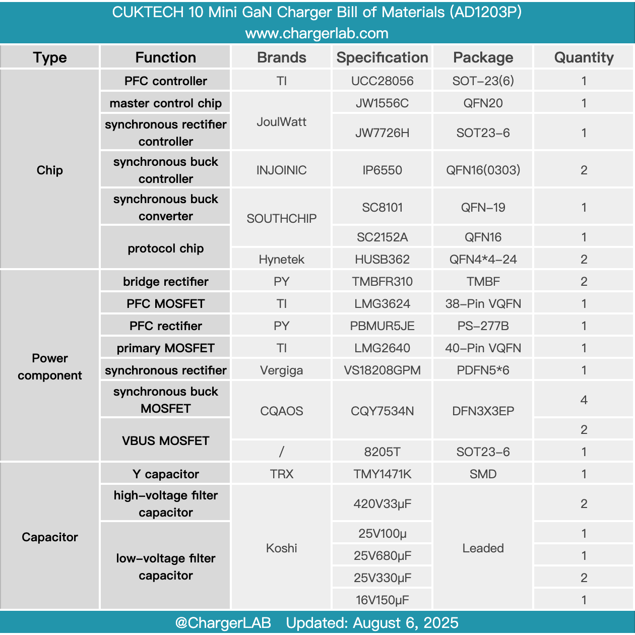
Here is the component list of the CUKTECH 10 Mini GaN Charger for your convenience.
Its design is compact and exquisite, and it comes with a 240W 6A USB-C cable. Both USB-C ports support Xiaomi’s 120W proprietary fast charging protocol, as well as 100W PD and 60W UFCS. The USB-A port supports 33W UFCS and 22.5W SCP. Featuring a GaN design and a custom TOB high-integration planar transformer, it achieves a smaller size and higher efficiency. The charger offers nine layers of safety protection, including short circuit, overvoltage, and overcurrent protection, and has passed CCC certification, ensuring reliable quality.
After taking it apart, we found that it adopts a PFC + AHB power architecture with three-channel secondary step-down outputs using synchronous rectification. The power solution includes the TI UCC28056 PFC controller and JOULWATT’s JW1556C + JW7726H combo, along with two GaN devices from TI: the LMG3624 and LMG2640.
The two USB-C ports use a pair of Injoinic IP6550 chips for synchronous buck conversion, with two Hynetek HUSB362 protocol chips managing output control. The USB-A port uses the SouthChip SC8101 for synchronous buck conversion, with output controlled by the SC2152A. The PCBA module is potted as a single unit for enhanced stability, and heatsinks are included to assist with thermal dissipation. Overall, the build quality and component selection are highly reliable.
Related Articles:
1. Teardown of StarCharge 7kW Smart AC Charger (AC0070GB060)
2. Teardown of UGREEN Thunderbolt 5 80Gbps M.2 NVMe SSD Enclosure (D705)
3. Teardown of OPPO 10000mAh 22.5W Energy Jelly Power Bank (PBSV00)