Introduction
In this issue, we present a teardown of a 67W dual USB-C GaN charger from Belkin. The charger supports 67W power output with unrestricted port usage, as well as a 45W + 20W power distribution strategy when both ports are in use. It also adopts a zero-standby-power energy-saving power supply design and integrates advanced gallium nitride power devices, delivering improved system reliability and efficiency compared with conventional power supplies. Below, we take a closer look at the detailed design and internal components of this charger.
Product Appearance
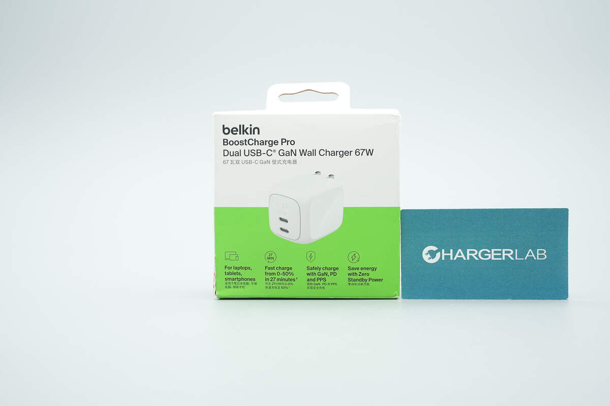
The front of the packaging box features the Belkin logo, the product name, an image of the charger, and its key selling points.
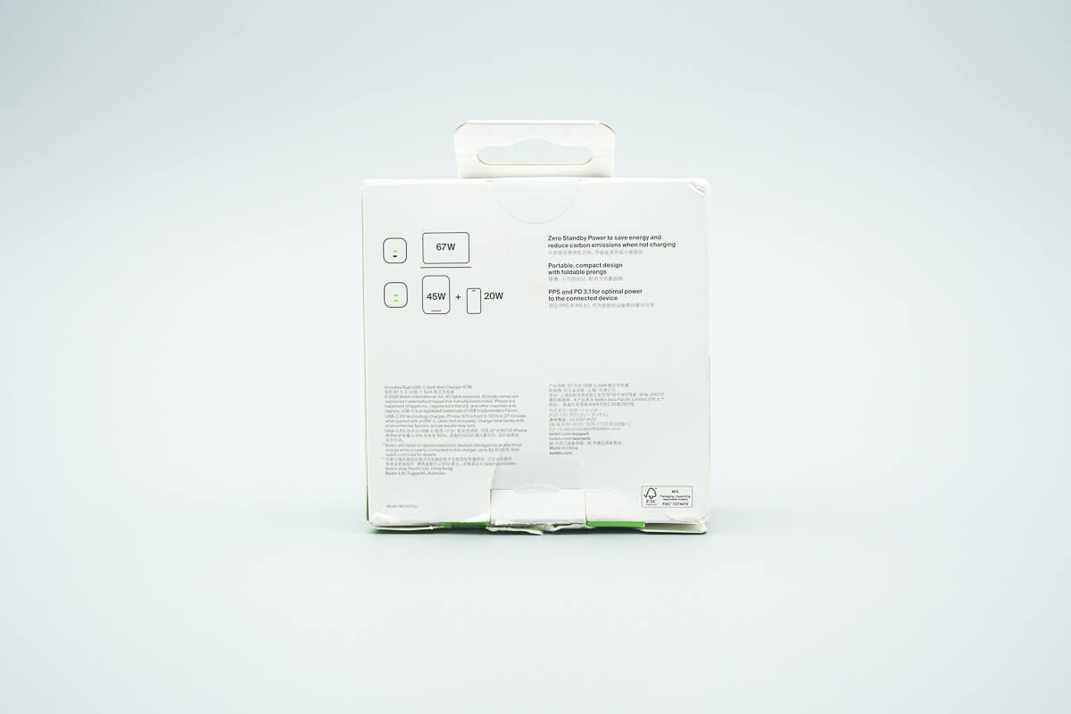
The back of the packaging is printed with the product’s technical specifications.
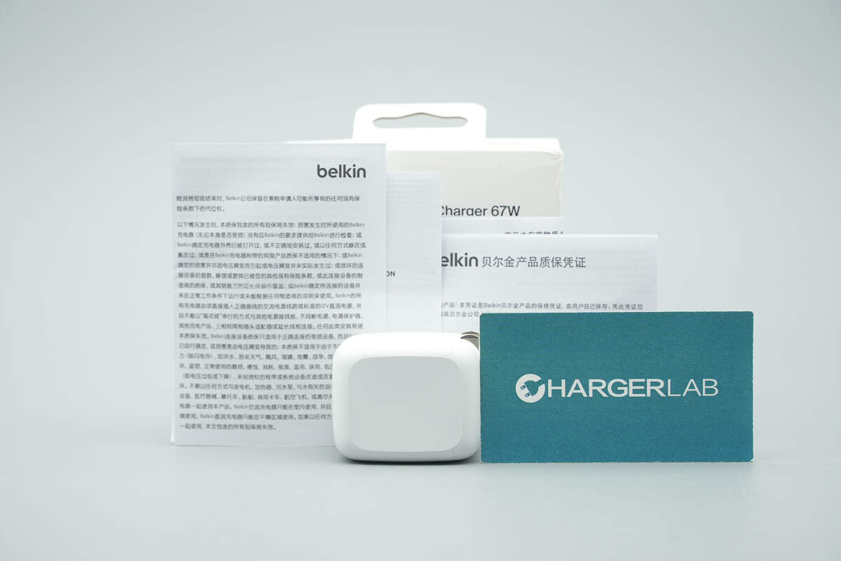
The package includes the charger, a user manual, and other documents.
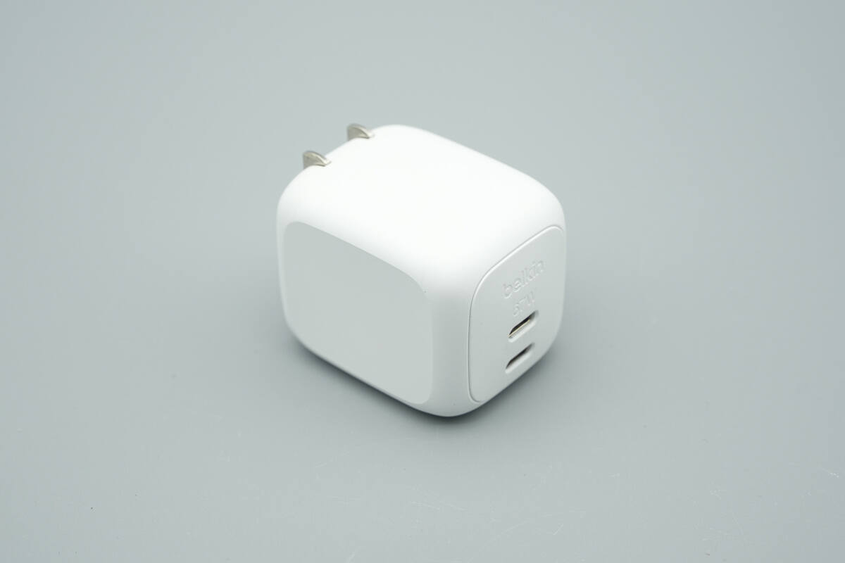
It features a compact form factor.
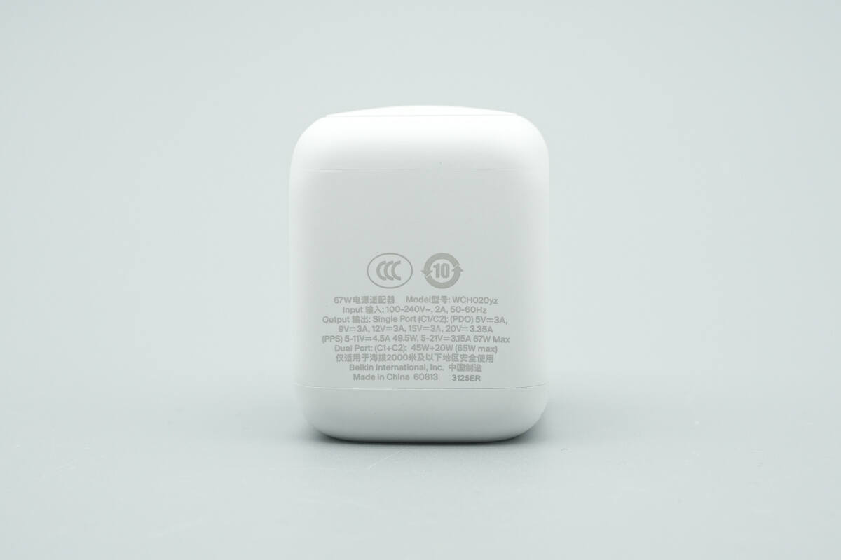
The product specifications are printed on the back.
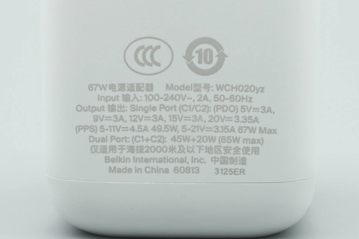
Model: WCH020yz
Input: 100–240V~ 50/60Hz 2A
Single-port output:
USB-C1 / C2 (PDO): 5V⎓3A, 9V⎓3A, 12V⎓3A, 15V⎓3A, 20V⎓3.35A
(PPS): 5–11V⎓4.5A, 5–21V⎓3.15A
Dual-port output:
C1 + C2: 45W + 20W (65W Max)
The product has passed CCC certification.
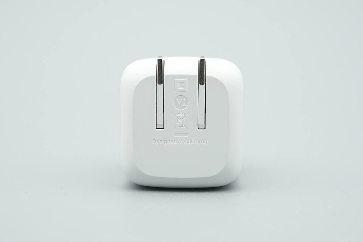
It has passed Level VI energy efficiency certification.
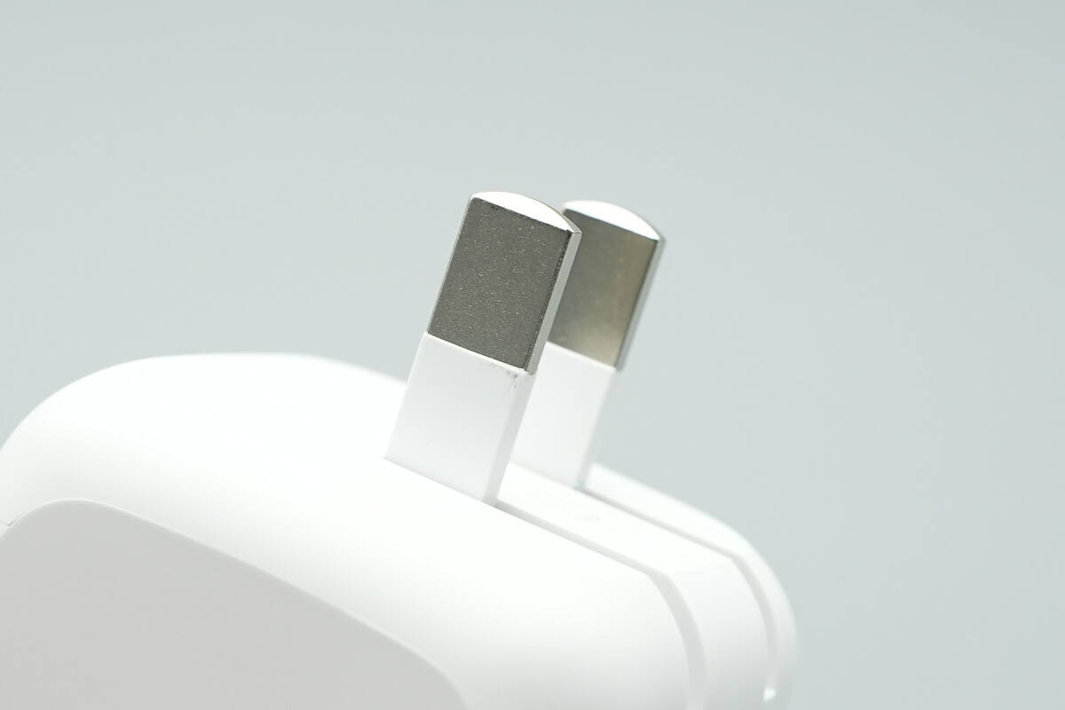
It is equipped with a foldable plug.
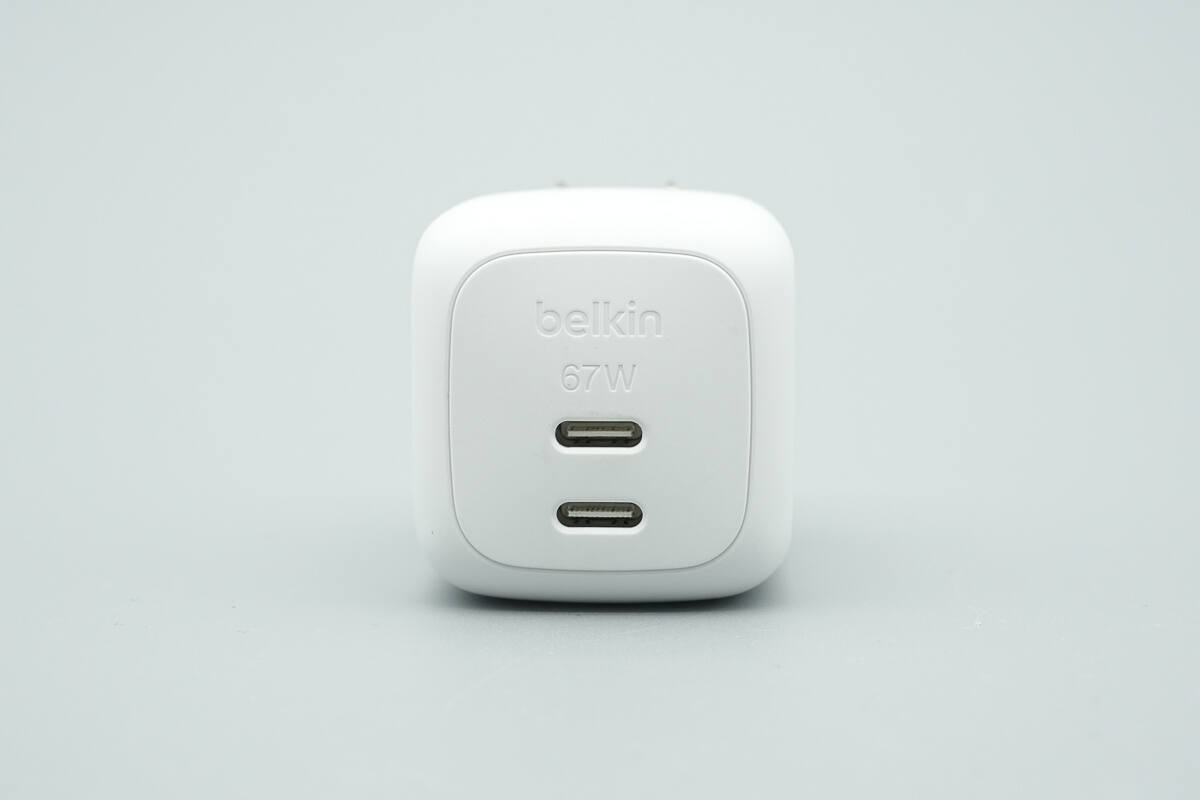
The output side features two USB-C ports, with "Belkin" and "67W" engraved above them.
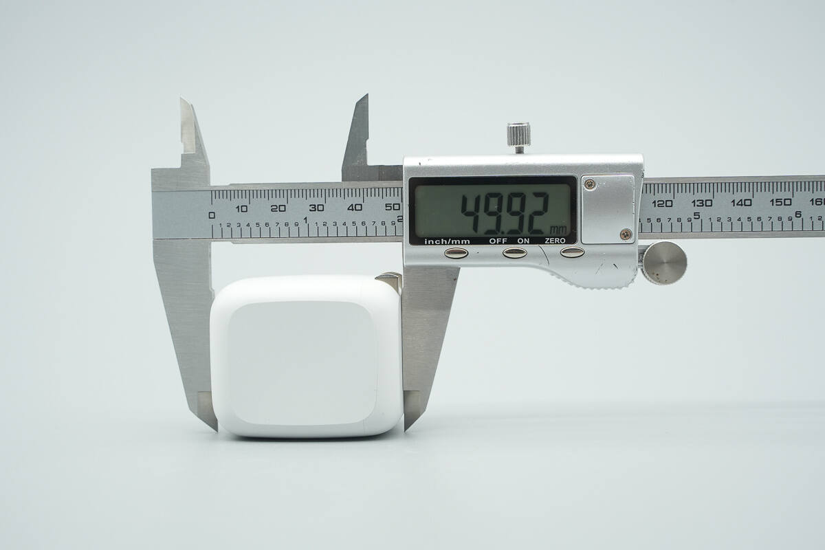
The length of the charger is about 49.92 mm (1.97 inches).
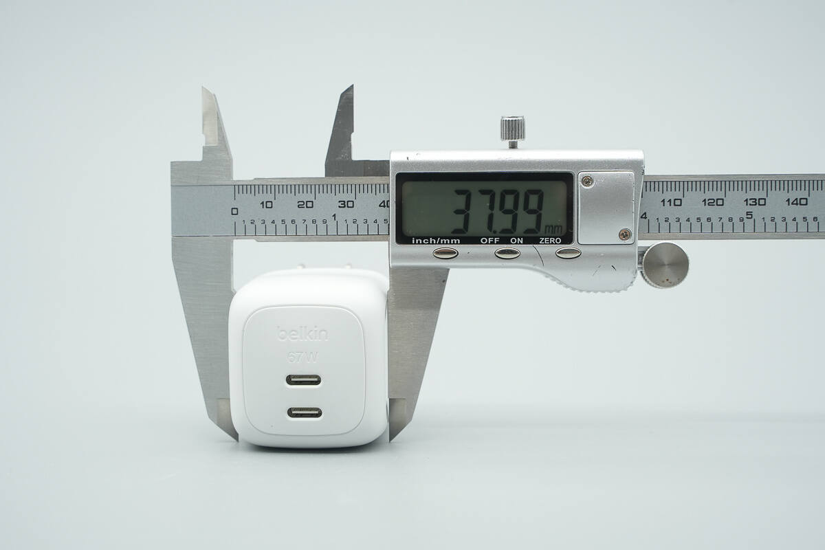
The width is about 37.99 mm (1.5 inches).
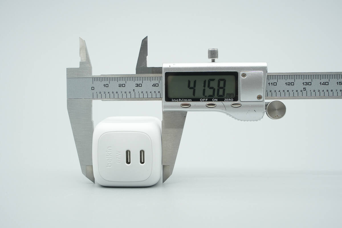
The thickness is about 41.58 mm (1.64 inches).
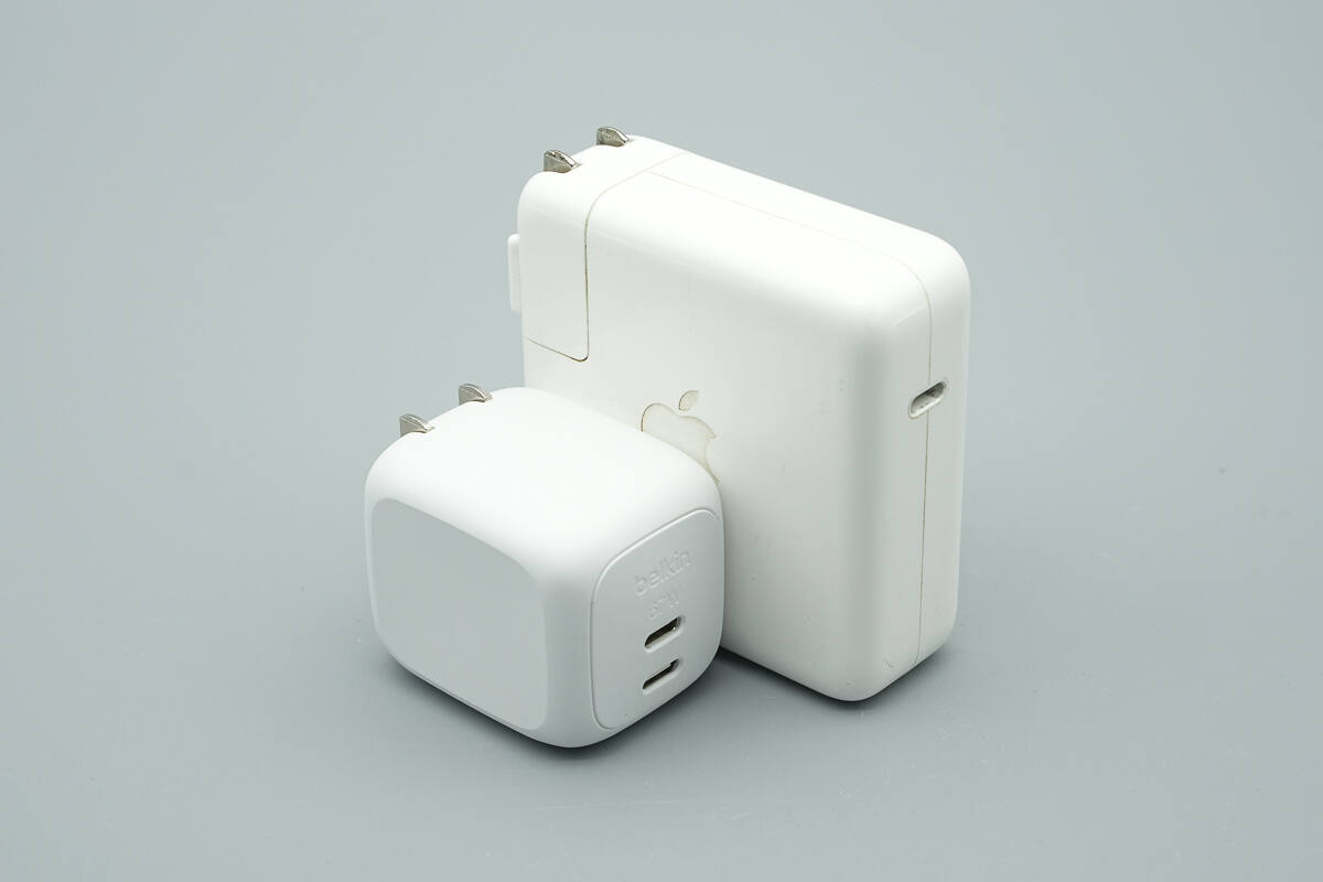
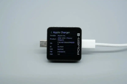
Compared with the Apple 67W charger, its size advantage is obvious.

That's how big it is on the hand.
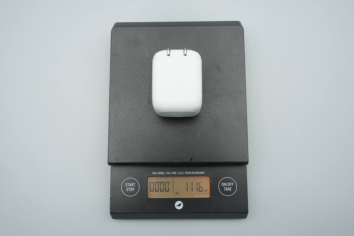
The weight is about 112 g (3.95 oz).
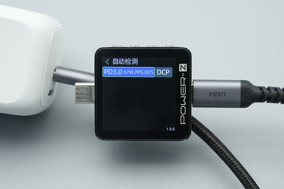
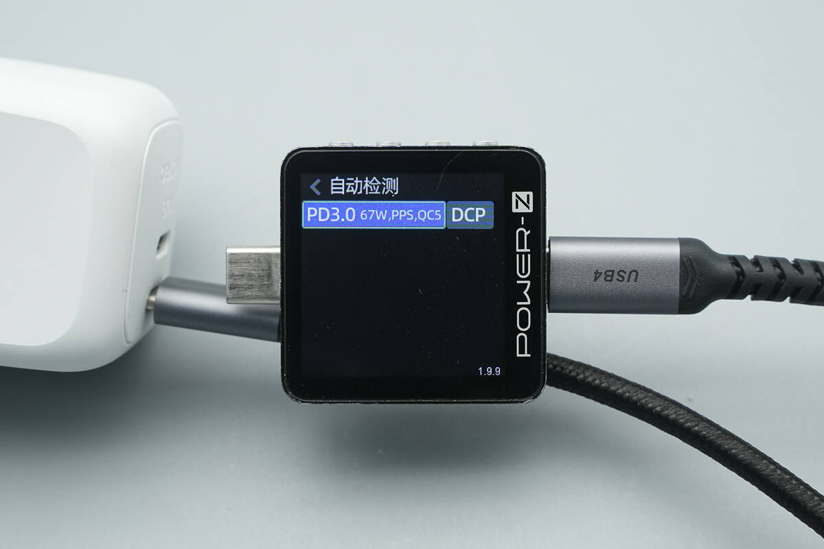
ChargerLAB POWER-Z KM003C shows that the USB-C1 supports PD3.0, PPS, QC5, and DCP protocols.
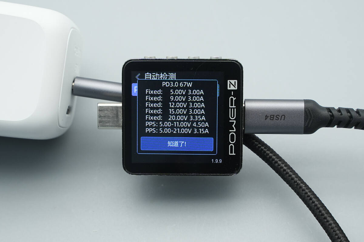
It has five fixed PDOs of 5V3A, 9V3A, 12V3A, 15V3A, and 20V3.35A, along with two sets of PPS, which are 5-11V4.5A and 5-21V3.15A.
The USB-C2 port supports the same protocols as the USB-C1 port.
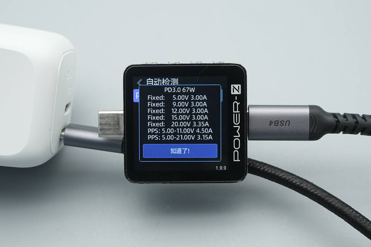
The PDO profiles are also identical.
Teardown
Next, let's take it apart to see its internal components and structure.
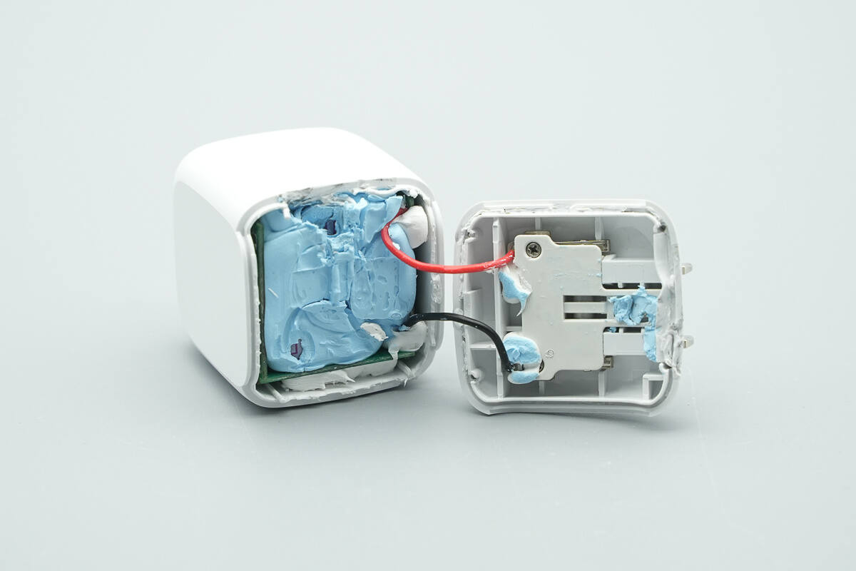
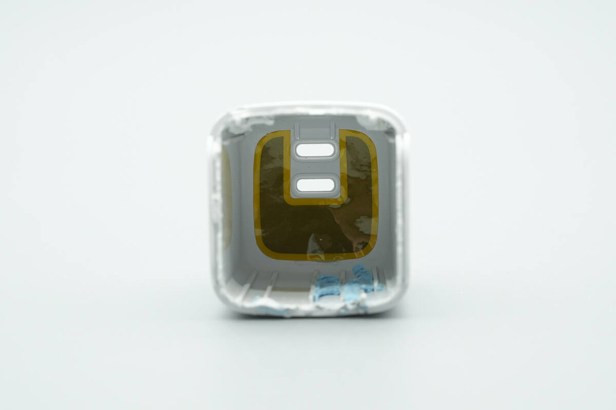
Cut open the input-side casing. The plug is secured with a plastic plate and screws.

The connecting wires are secured with adhesive for protection.
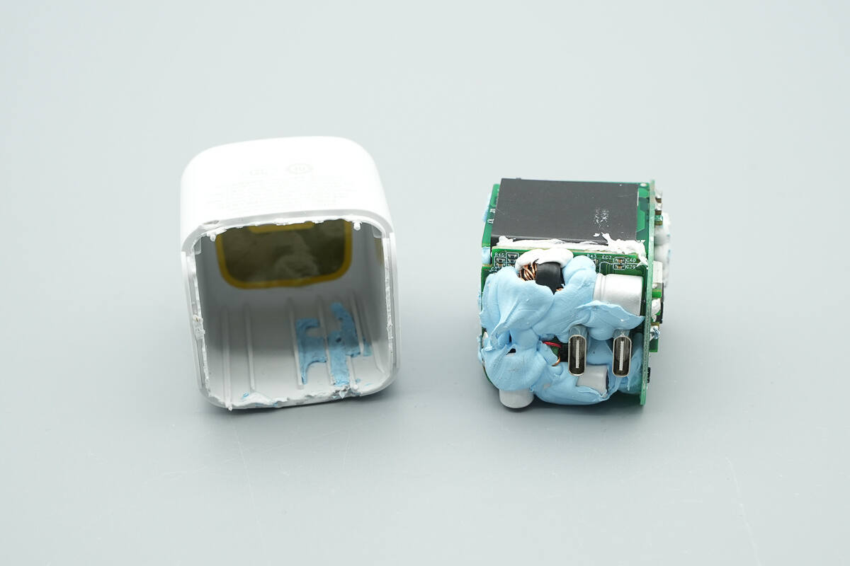
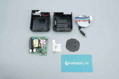
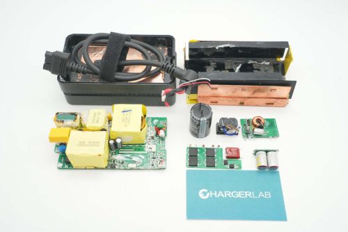
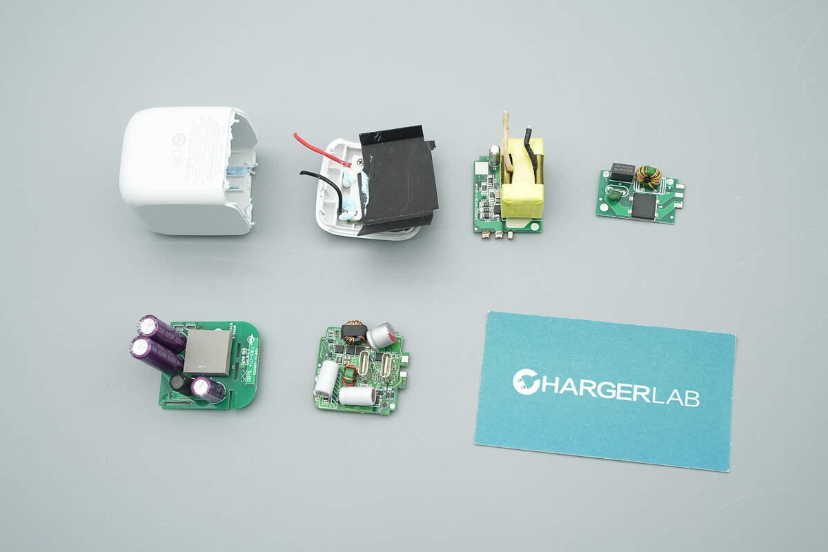
Remove the PCBA module.
The inner side of the casing is lined with a graphite thermal pad.
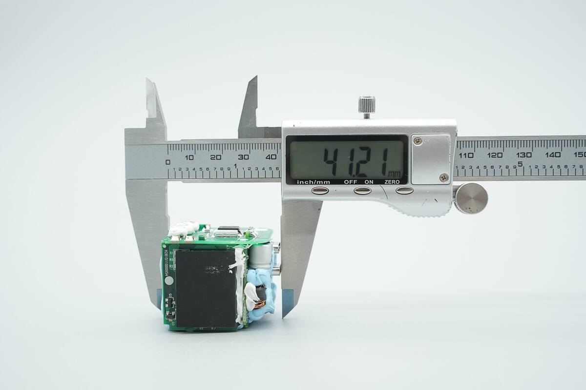
The length of the PCBA module is about 41.21 mm (1.62 inches).
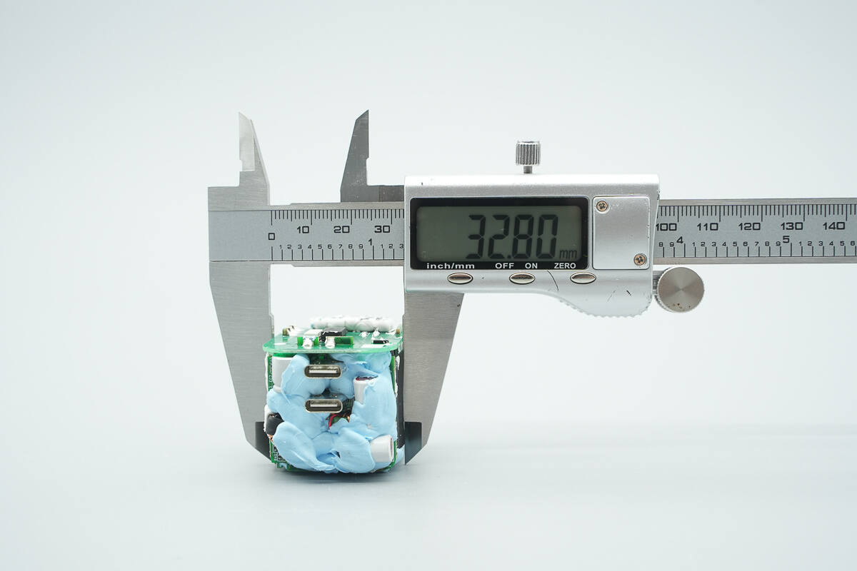
The width is about 32.8 mm (1.29 inches).

The thickness is about 35.64 mm (1.4 inches).
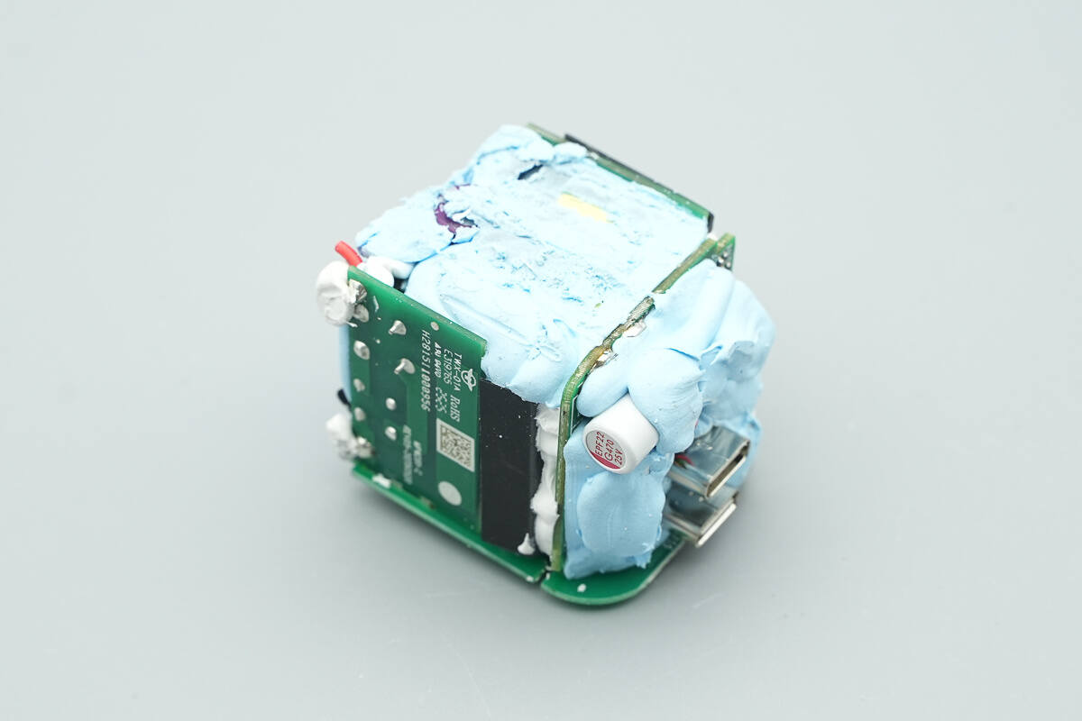
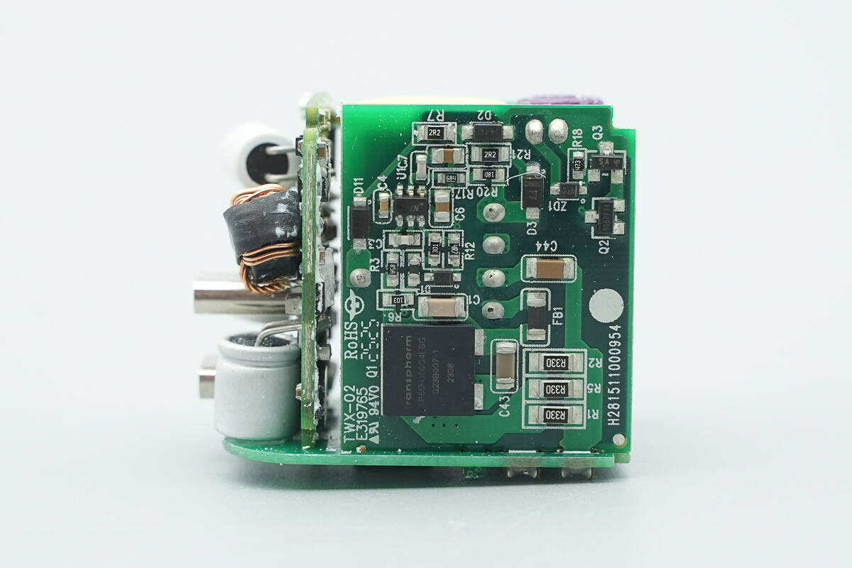
The PCBA module consists of multiple small stacked PCBs, with extensive adhesive applied on the module for reinforcement and heat dissipation.
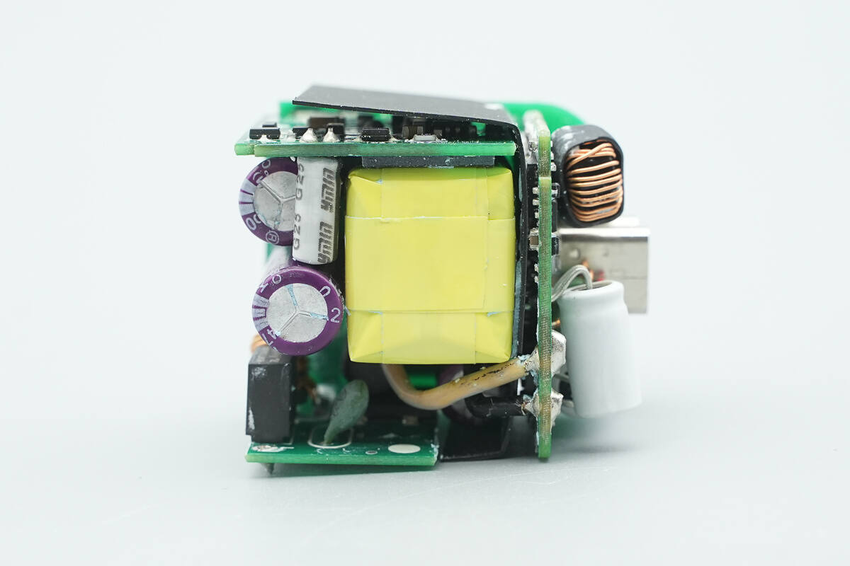
After removing the adhesive, the front of the module reveals three small PCBs, making efficient use of the available space. A Mylar sheet is also placed between the primary and secondary sides for insulation.
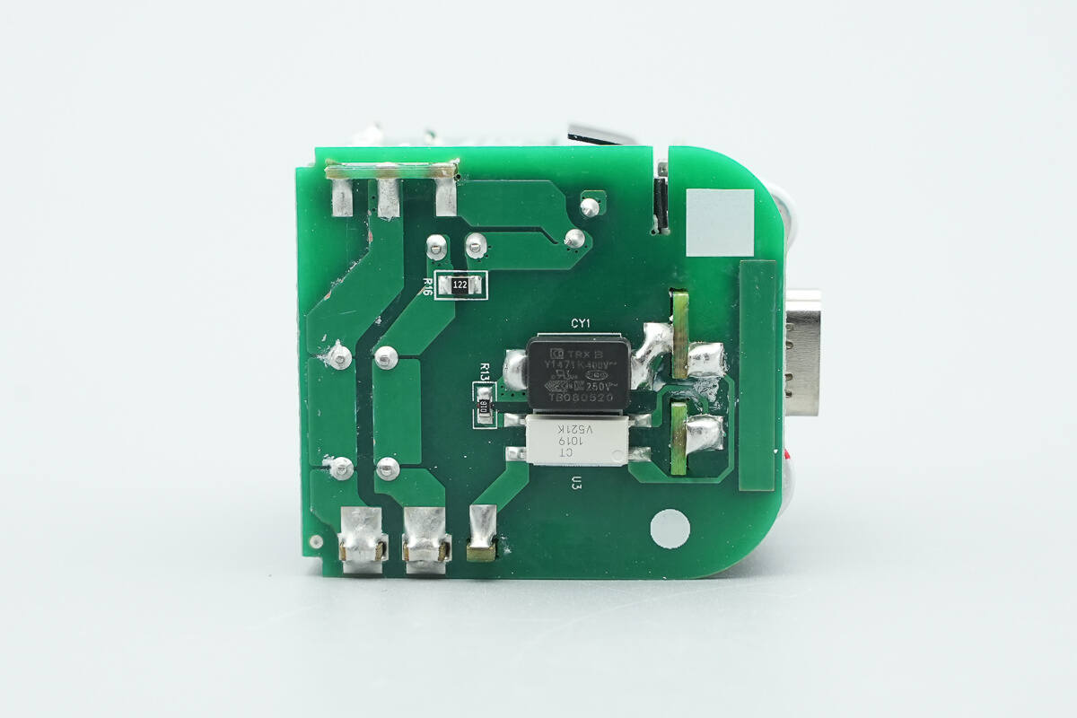
The back side features an SMD Y capacitor and an optocoupler.
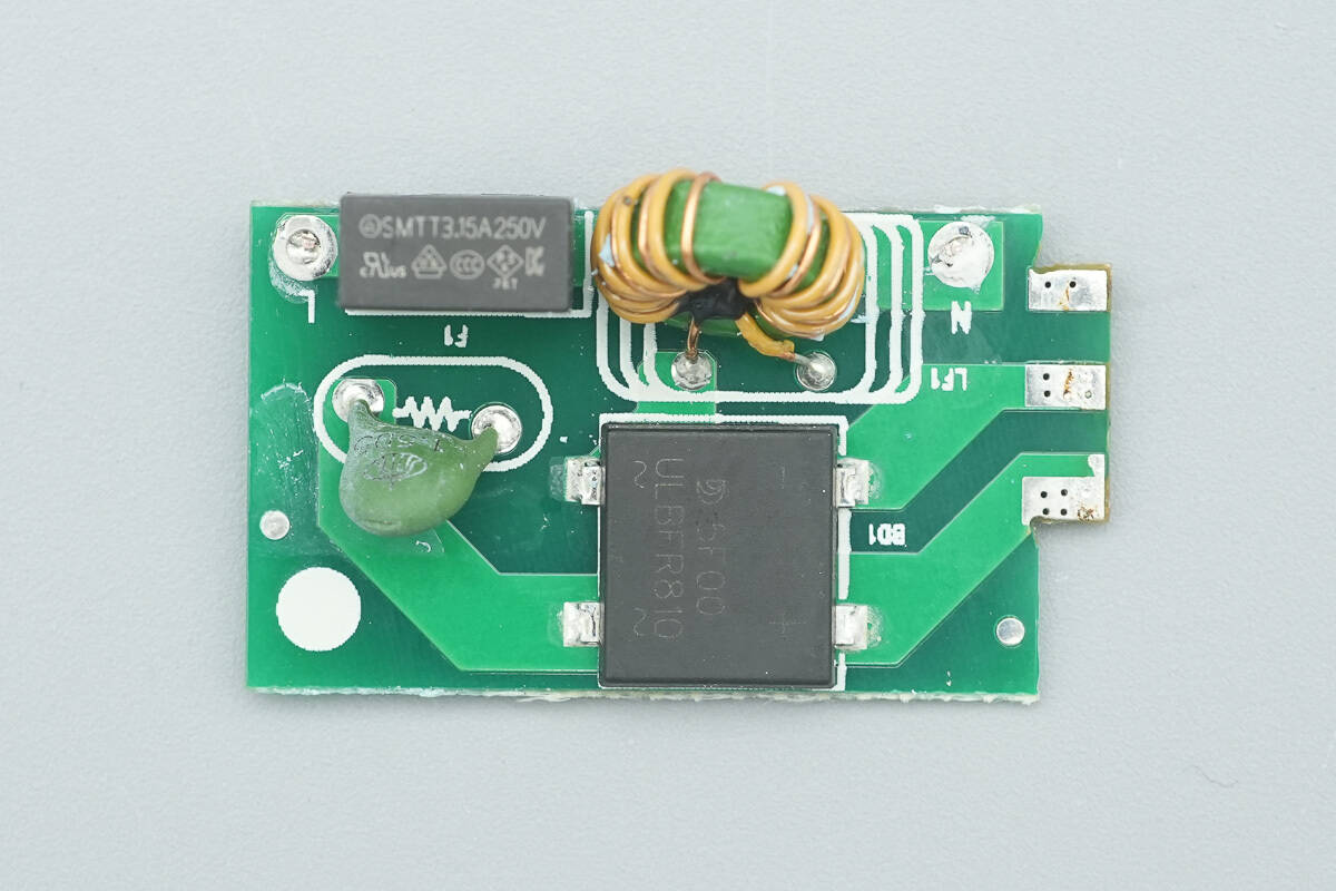
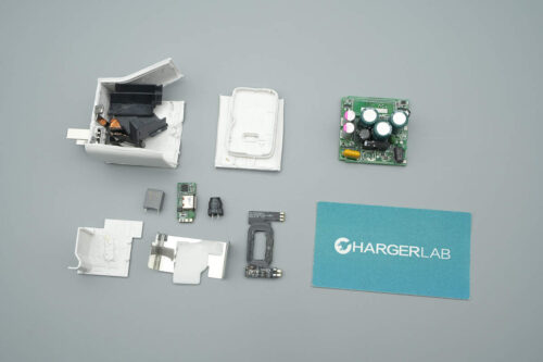
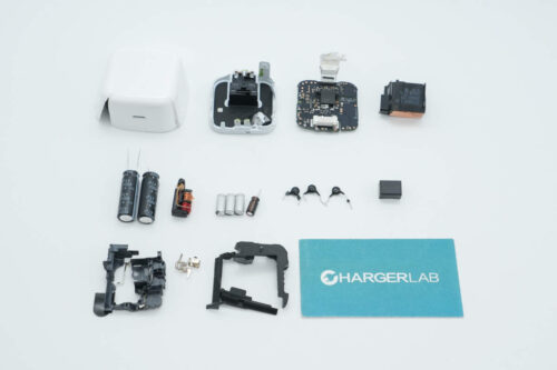
Remove one of the small PCBs. Its front side is equipped with a time-delay fuse, an NTC thermistor, a common mode choke, and a bridge rectifier.
The back side of the small PCB has no components.
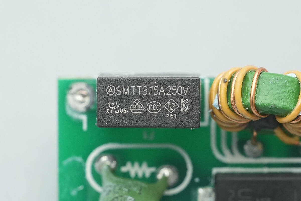
The time-delay fuse is rated at 3.15 A, 250 V.

The NTC thermistor from Shiheng is used to suppress inrush current during power-on.
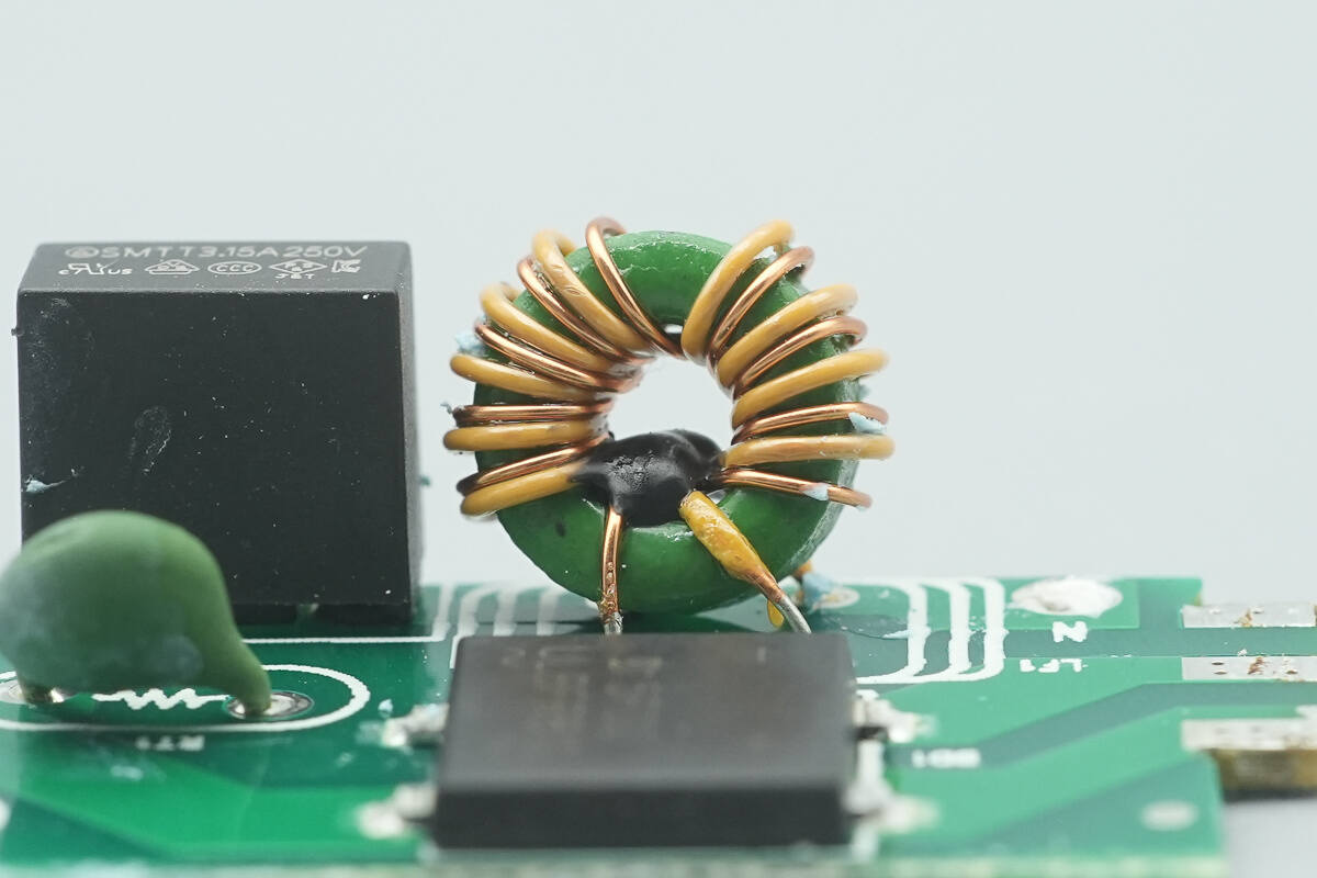
The common mode choke is used to filter out EMI interference.
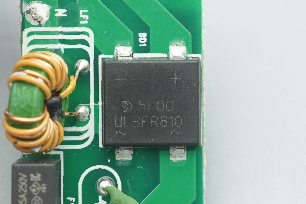
The ULBFR810 bridge rectifier is rated at 8 A, 1000 V, and comes in a ULBF package.
On the other small PCB, there is a master control chip and a primary MOSFET.
The PCBA module is fully disassembled.
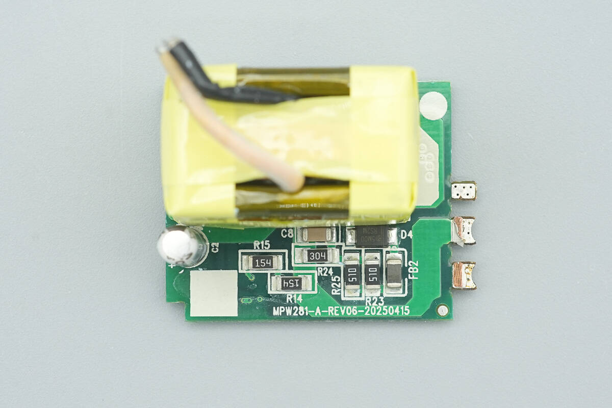
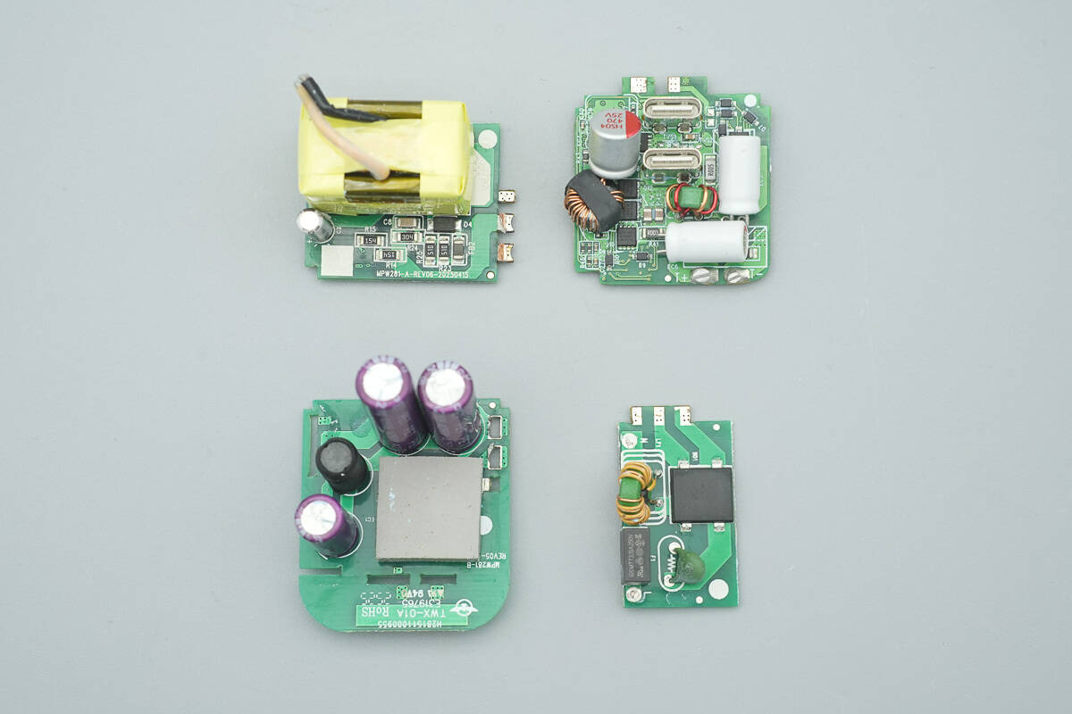
The front side of the small PCB also features a transformer and a capacitor that supplies power to the master control chip.
There are three electrolytic capacitors and one I-shaped inductor, with a thermal pad positioned beneath the transformer.
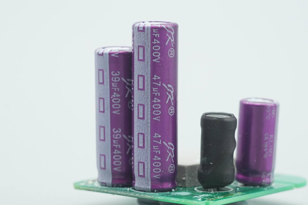
All three electrolytic capacitors are from JK, with one rated at 400 V, 47 μF.

The second capacitor is rated at 400 V, 39 μF.
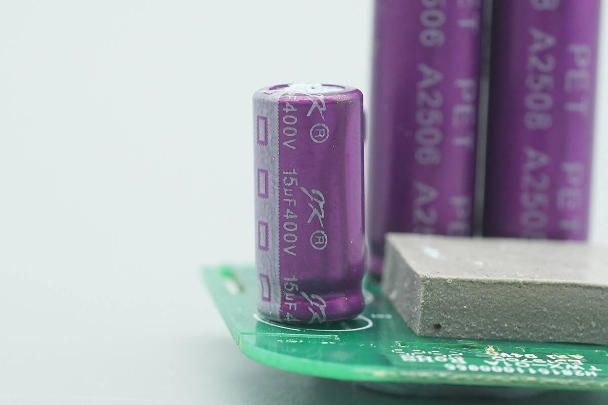
The third capacitor is rated at 400 V, 15 μF.
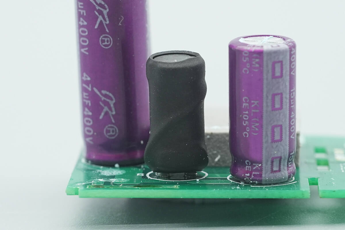
The I-shaped inductor is covered with heat-shrink tubing for insulation and protection.
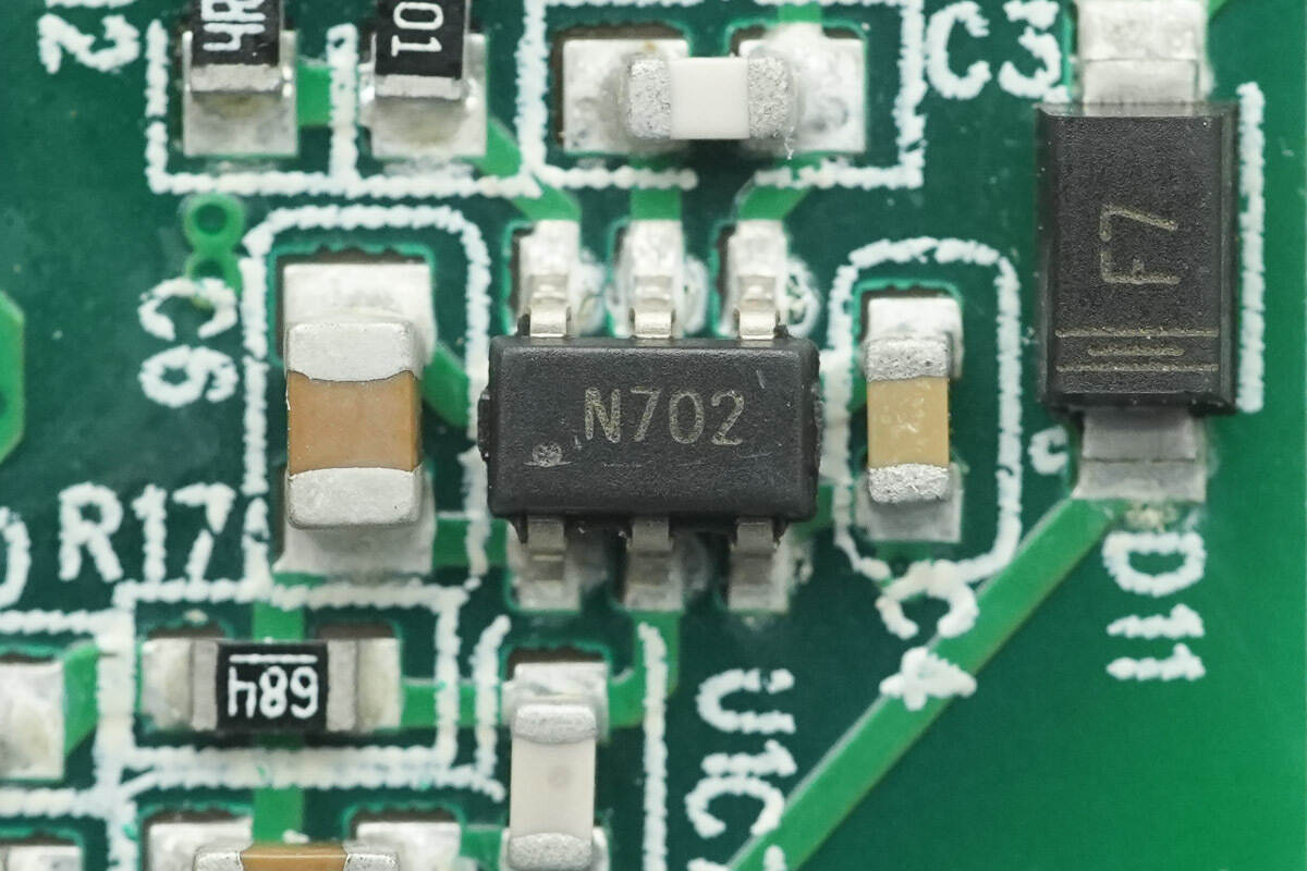
The master control chip is from RENESAS, marked with N7, model is iW9870, and comes in a SOT-23-6 package.
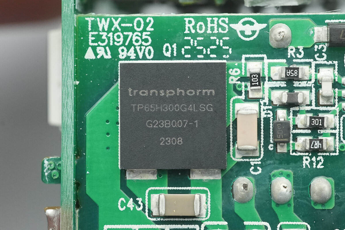
The primary MOSFET is from RENESAS, model TP65H300G4LSG, with a voltage rating of 650 V and an on-resistance of 240 mΩ. It utilizes advanced epi and patented design technologies to simplify the manufacturing process and reduce costs, while improving silicon efficiency by lowering gate charge, output capacitance, cross-conduction losses, and reverse recovery charge. The device comes in a DFN 8×8 mm package.
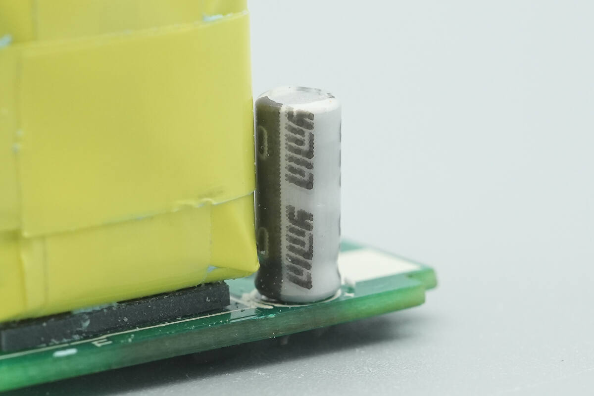
The capacitor supplying power to the master control chip is from YMIN.
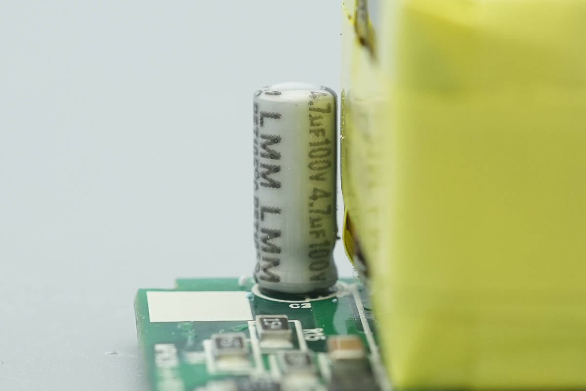
It is rated at 100 V, 4.7 μF.
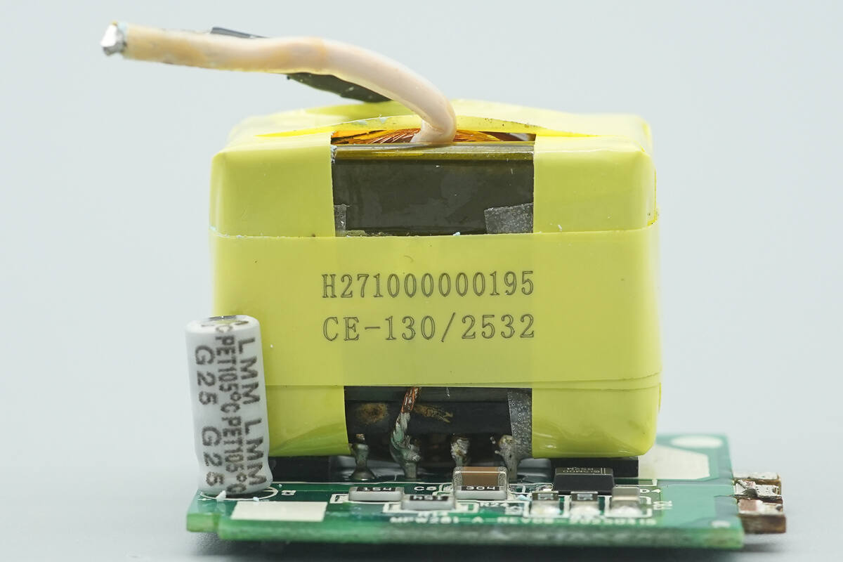
Close-up of the transformer.
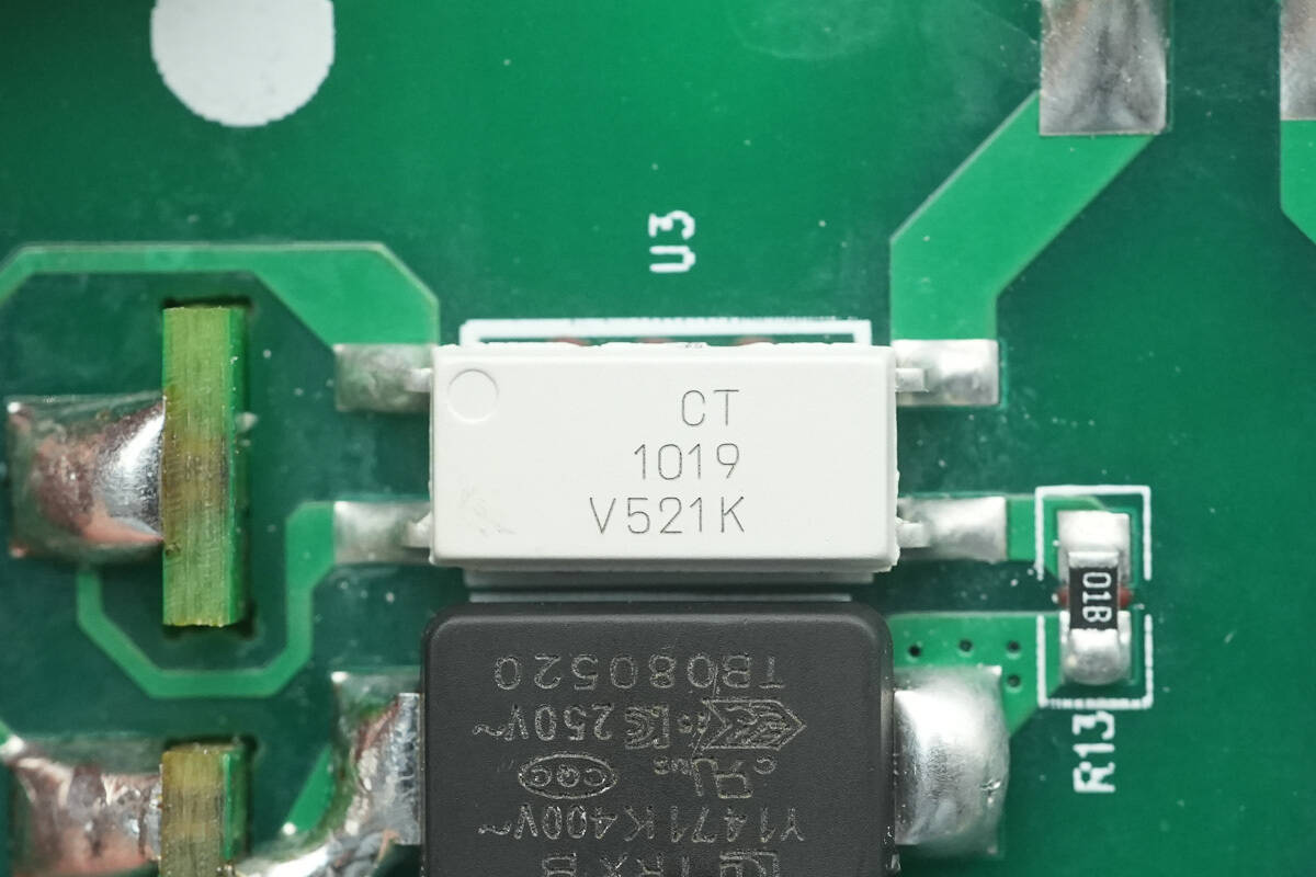
The CT1019 optocoupler is used for output voltage feedback.
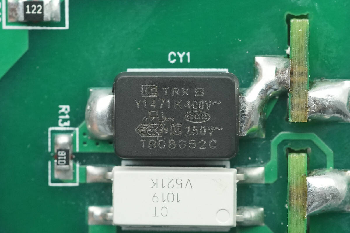
The SMD Y capacitor is from TRX, part number TMY1471K. Its compact size and light weight make it well-suited for high-density power products such as GaN fast chargers.
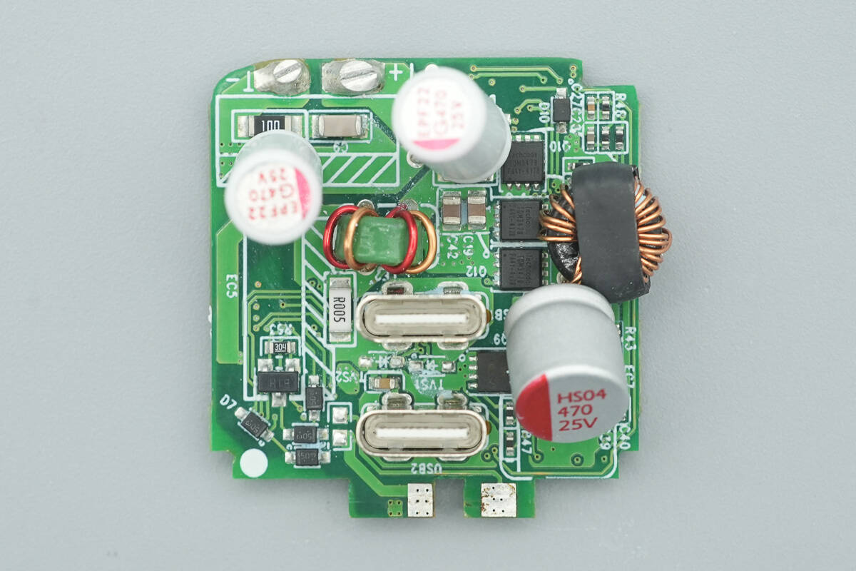
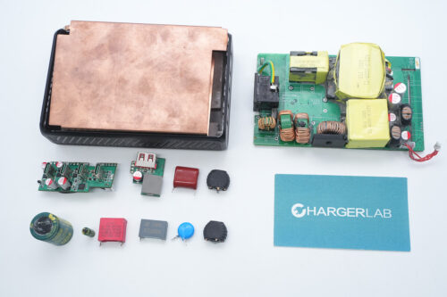
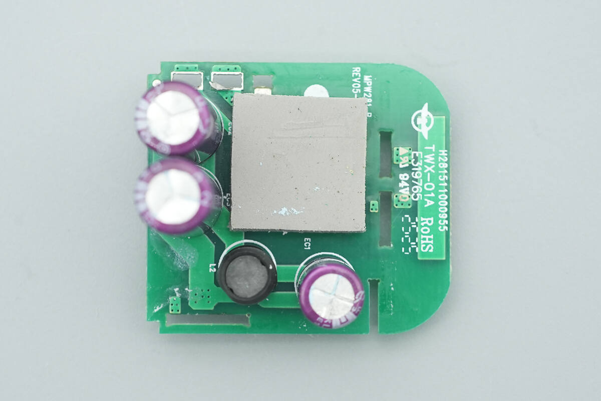
The front side of the output small PCB features synchronous buck MOSFETs, a buck inductor, solid capacitors, and a VBUS MOSFET, among other components.
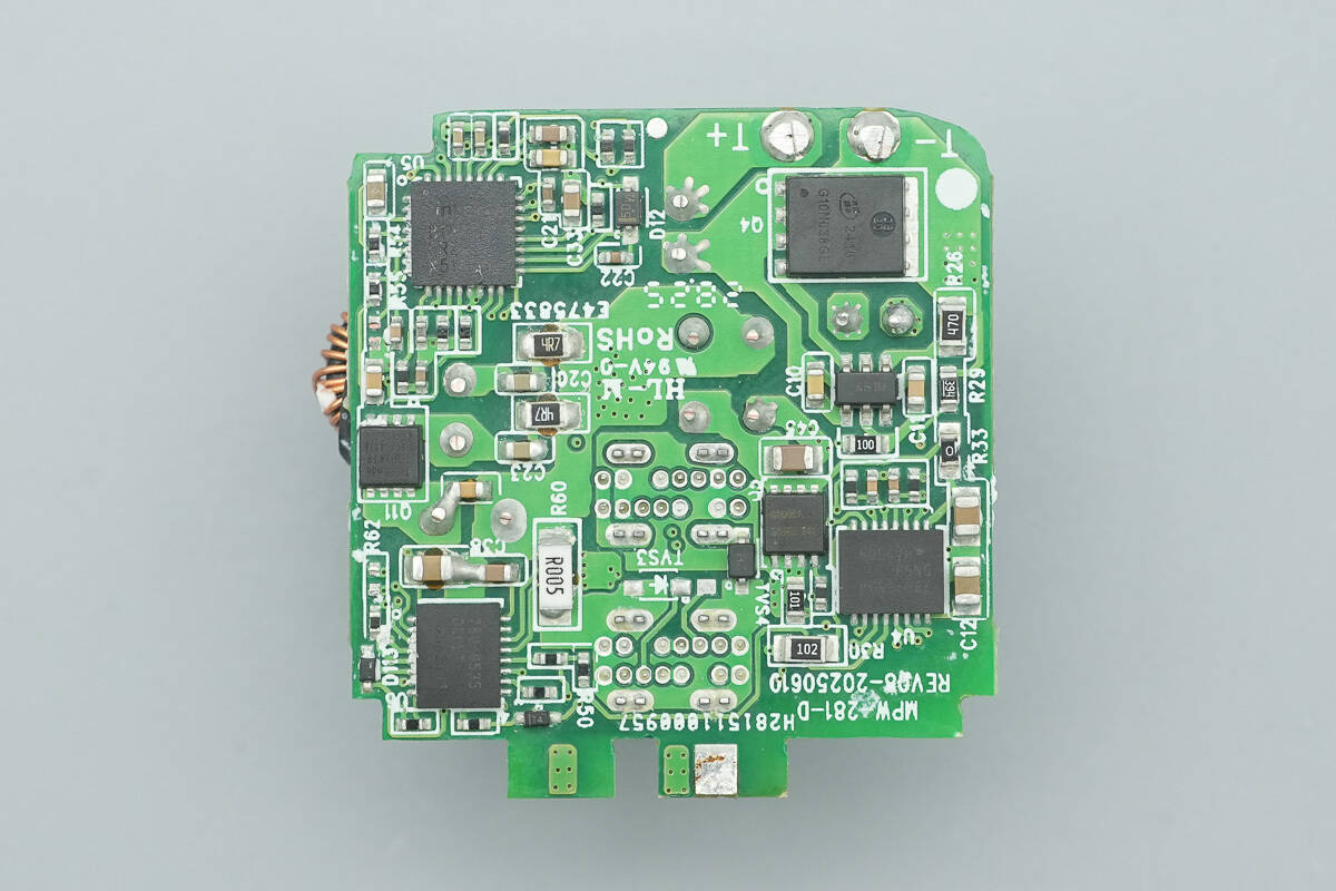
The back side houses a synchronous rectifier controller, a synchronous rectifier, a synchronous buck-boost controller, a synchronous buck MOSFET, protocol chips, and a VBUS MOSFET.
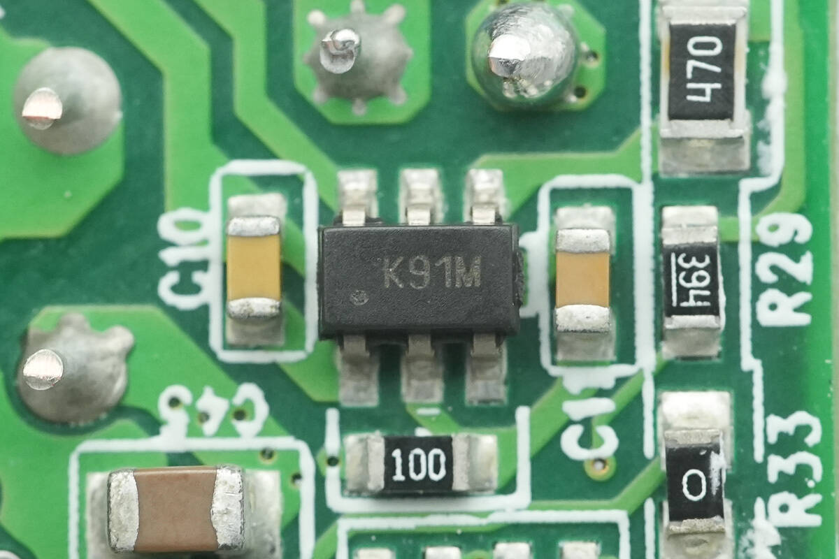
The synchronous rectifier controller is from RENESAS, marked with K9, model iW610-06, and integrates a MOSFET driver. RENESAS’ proprietary lossless VDS sensing and control technology allows it to support multiple AC/DC topologies, including QR, DCM, CCM, ZVS, and ACF. It comes in a SOT-23-6 package.
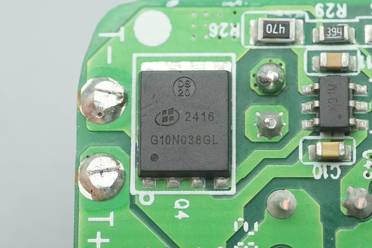
The synchronous rectifier is from ALKAIDSEMI, model AKG10N038GL. It is an NMOS with a voltage rating of 100 V and an on-resistance of 3.8 mΩ, packaged in a PDFN 5×6 mm case.
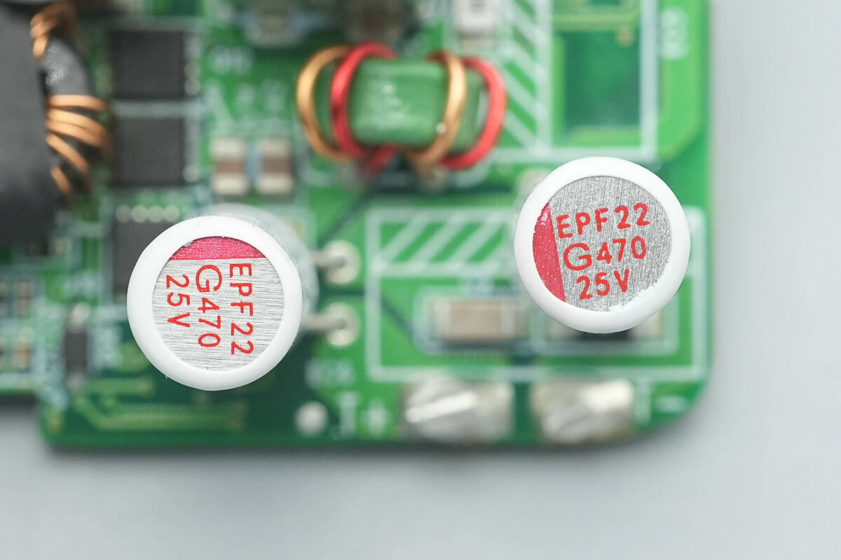
The two solid capacitors are covered with plastic insulation sleeves, each rated at 25 V, 470 μF.
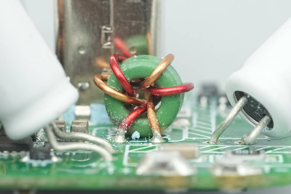
Close-up of the filter inductor.
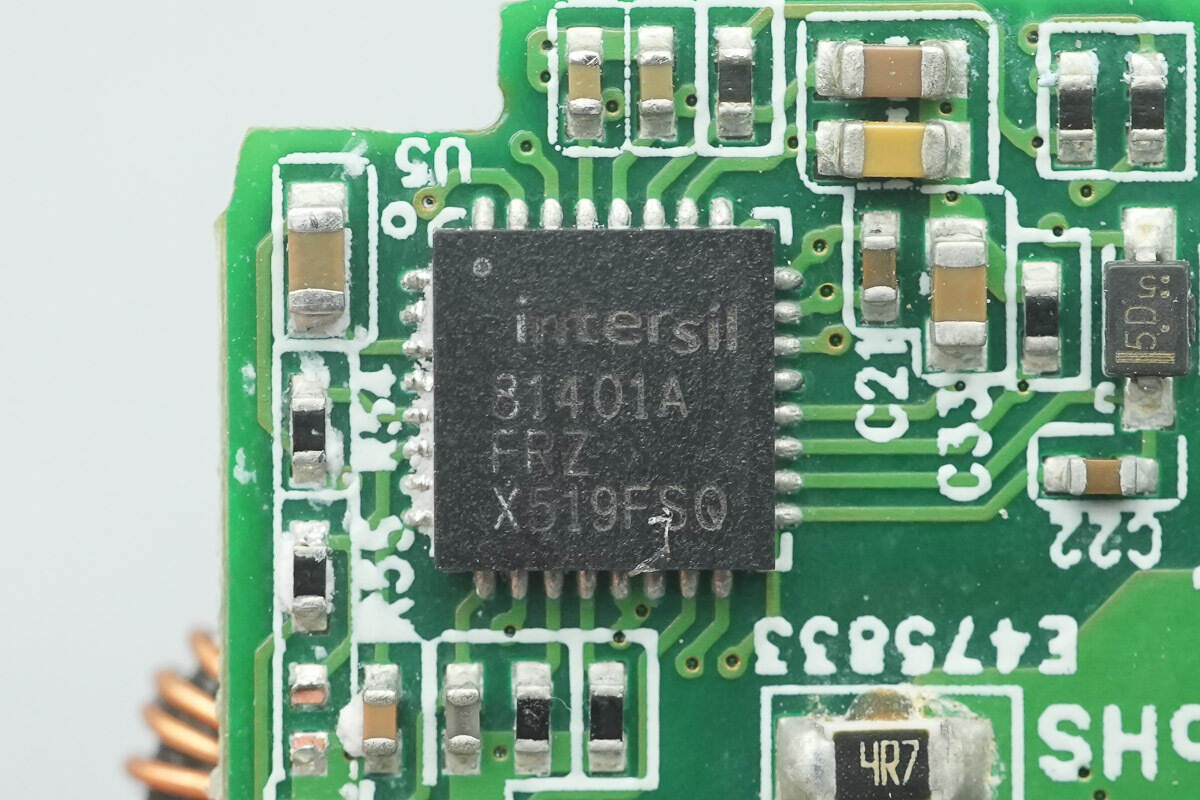
The synchronous buck-boost controller is from RENESAS, model ISL81401A. It is a four-switch controller supporting a wide input voltage range of 4.5–40 V and an output voltage range of 0.8–40 V. The switching frequency is programmable from 100 kHz to 600 kHz. It provides comprehensive protection features, including over-voltage protection, under-voltage protection, over-temperature protection, and both average and peak current limits at the input and output, ensuring high reliability in both step-up and step-down operations. The device comes in a QFN-32 package.
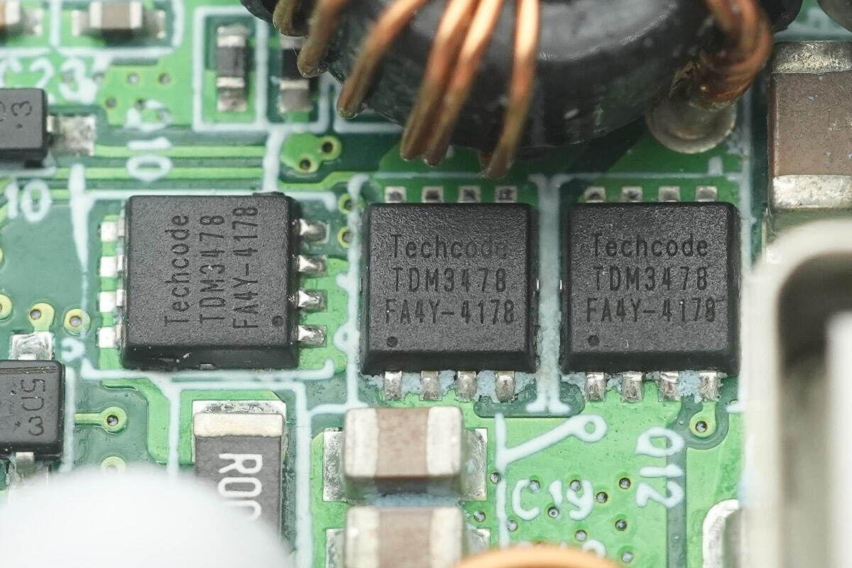
The four synchronous buck MOSFETs are from Techcode, model TDM3478. They are NMOS with a voltage rating of 30 V and an on-resistance of 5 mΩ, packaged in PPAK 3×3-8 cases.
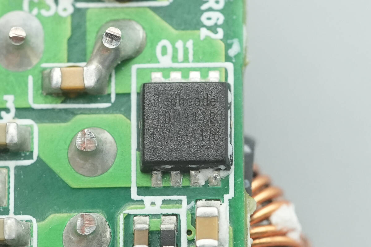
One of them is located on the back side of the small PCB.
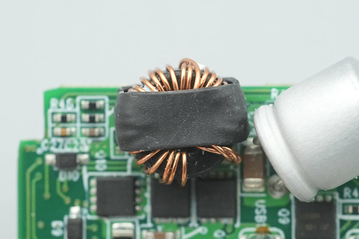
Close-up of the buck inductor.
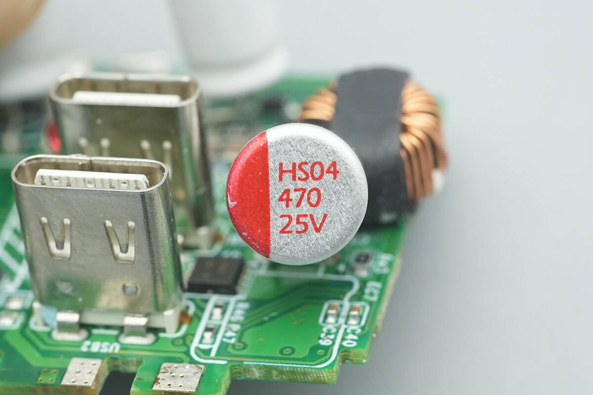
The buck output filter solid capacitor is rated at 25 V, 470 μF.
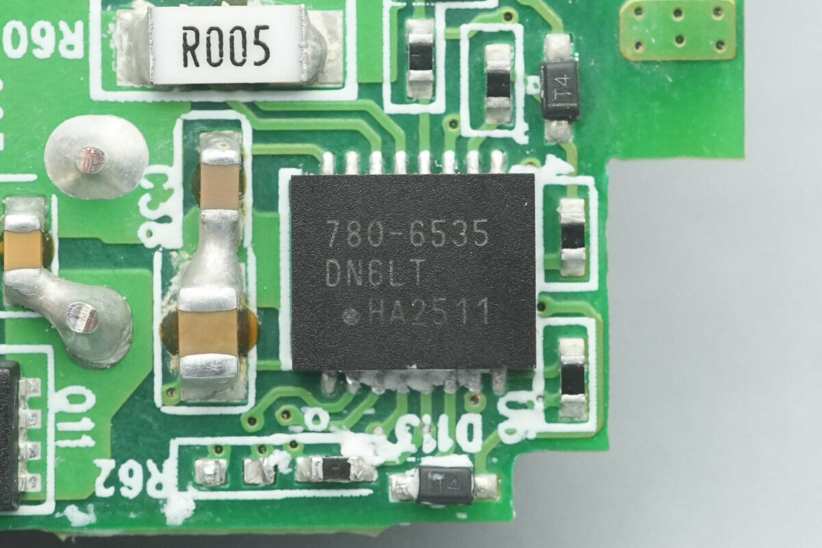
The USB-C1 protocol chip is from RENESAS, model iW780. It is a programmable AC/DC multi-protocol controller that integrates a secondary-side regulation controller, an interface protocol controller, and a USB VBUS NFET driver. It supports multiple fast-charging protocols, including PD3.1, PPS, UFCS, SCP, and QC3+. The device comes in a TDFN 16×5×4 mm package.
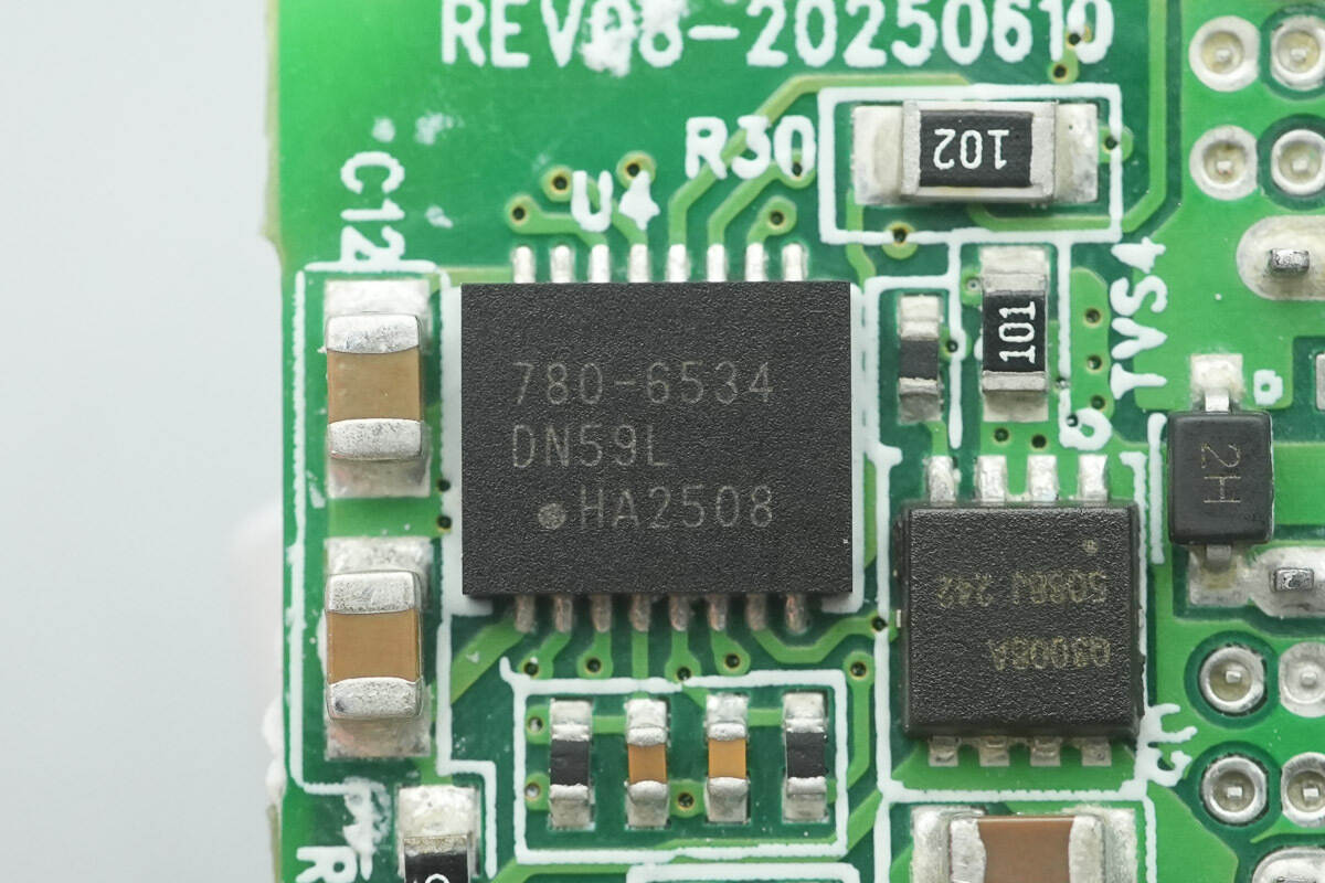
The protocol chip for the other port is also a RENESAS iW780.
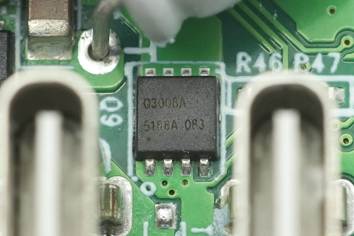
The output VBUS MOSFET is marked Q3008A and comes in a PDFN 3×3 mm package.
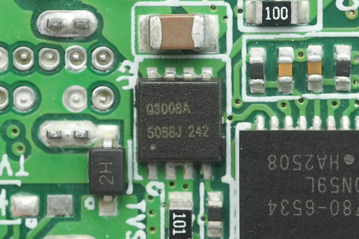
The other VBUS MOSFET has the same part number.
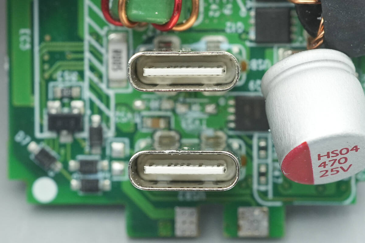
Close-up of the two USB-C sockets.
Well, those are all components of the Belkin BoostCharge Pro Dual USB-C 67W GaN Wall Charger.
Summary of ChargerLAB
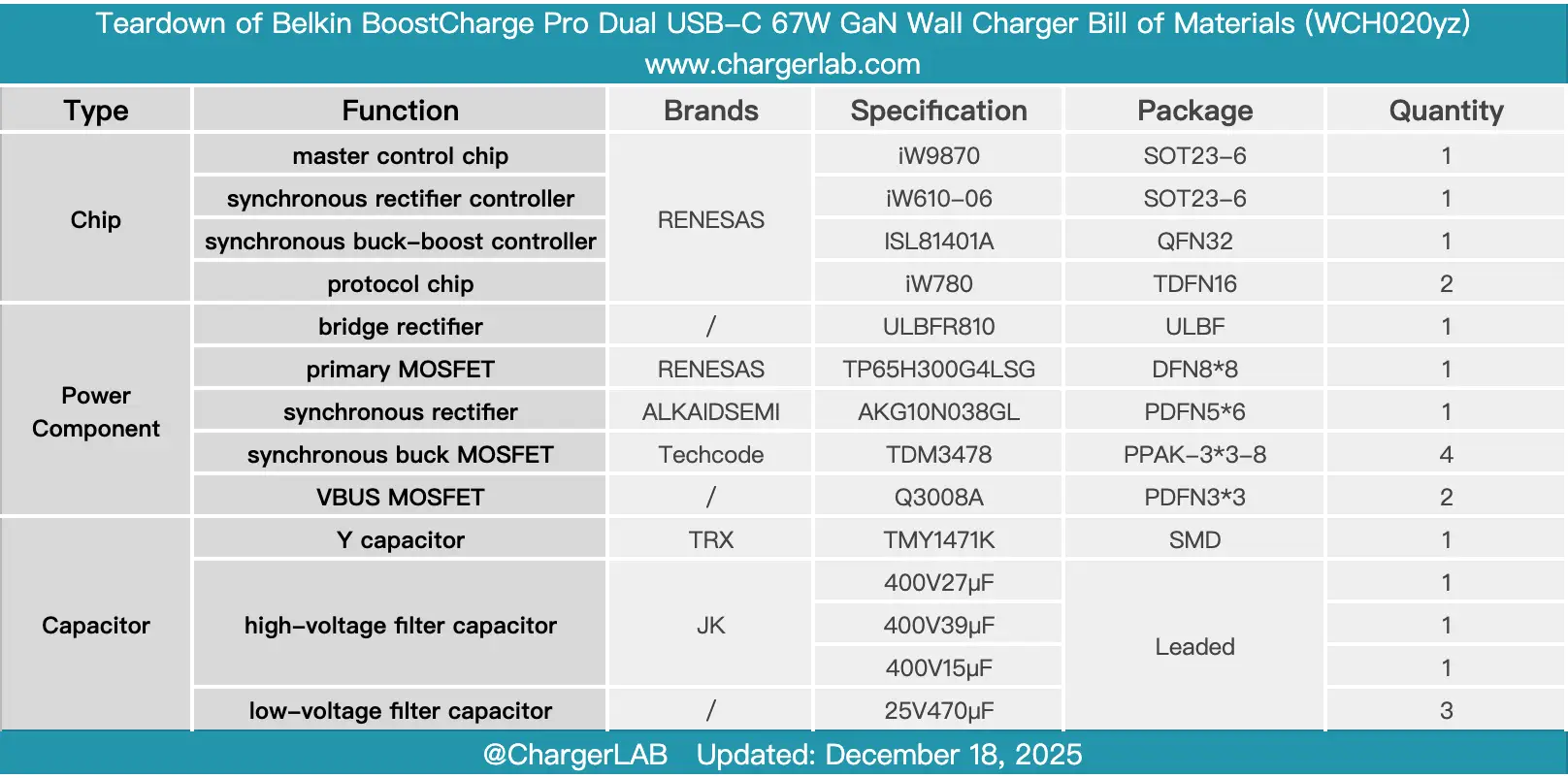
Here is the component list of the Belkin BoostCharge Pro Dual USB-C 67W GaN Wall Charger for your convenience.
It continues the series’ design language, combining a compact size with a foldable plug for portability. Both USB-C ports support up to 67 W output and are compatible with PD and PPS fast-charging protocols.
After taking it apart, we found that it uses multiple RENESAS components, including the power management solution, GaN devices, synchronous buck controllers, and protocol chips. This not only results in high overall integration and reliability, but the chip performance is also excellent. Additionally, the design employs a stacked configuration of four PCBs to maximize space utilization, with extensive adhesive applied for reinforcement and heat dissipation. The build quality and component selection are commendable.
Related Articles:
1. Teardown of Huawei SuperCharge 66W GaN Charger for Mate 80 (HW-110600C05)
2. Teardown of Huntkey 140W GaN Charger (HKC14028050-0B1)
3. Teardown of NIU 280W E-bike Charger (DZL482015N)