Introduction
Today, we take a look at the teardown of the Belkin BoostCharge Pro 140W 4-Port GaN Wall Charger. The charger is equipped with three USB-C ports and one USB-A port. The USB-C1 port supports PD3.1 with up to 140W output. USB-C2 and USB-C3 share a 65W power budget, while the USB-A port provides a fixed 12W output. This configuration makes it a single charger capable of meeting the charging needs of most users’ devices. Next, let’s take a closer look at its internal components and design.
Product Appearance
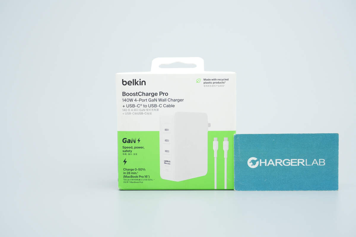
The front of the packaging displays the Belkin logo, the product name, an image of the charger, and its key selling points.
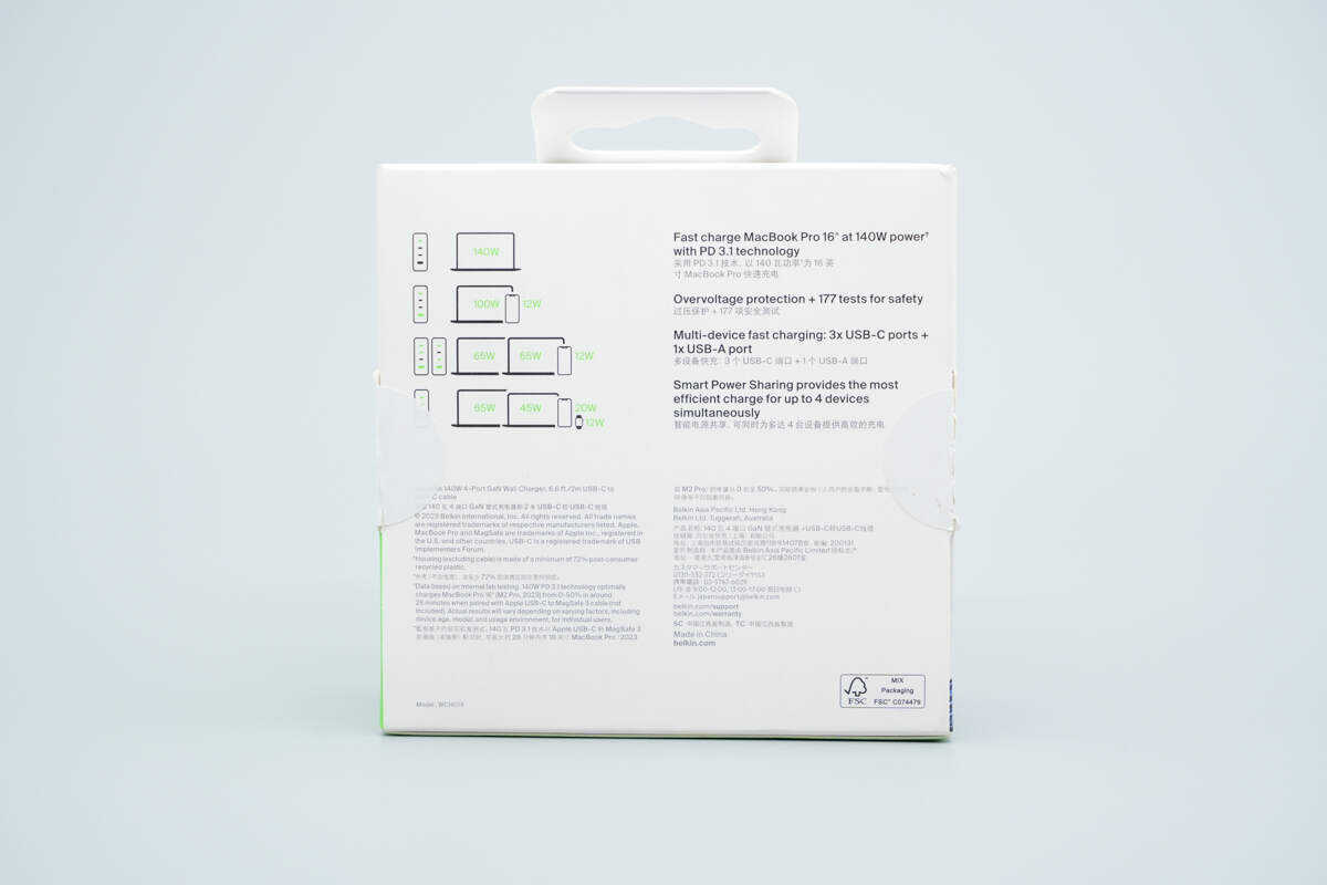
The back of the packaging features the product information.
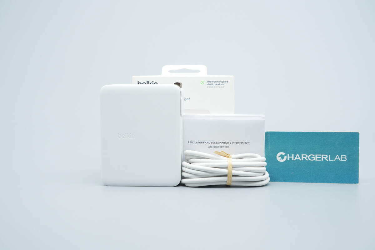
The package includes the charger, a data cable, and a user manual.
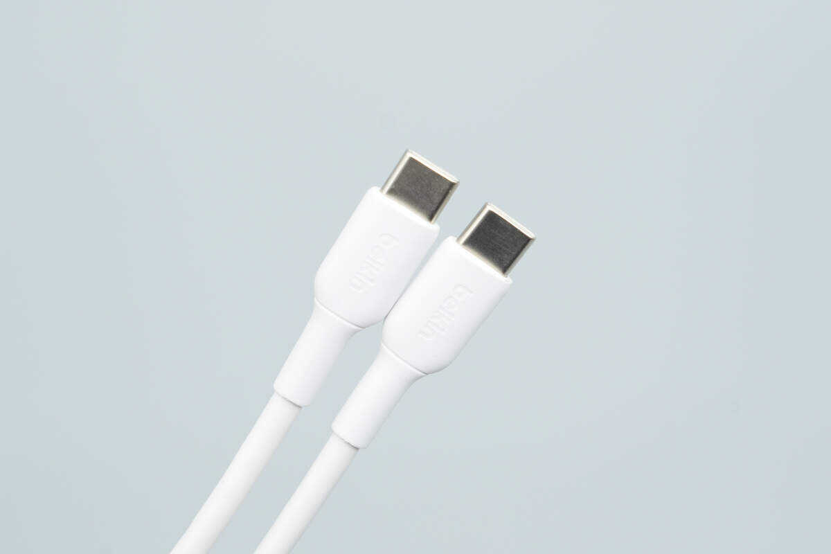
The included data cable is a dual USB-C type, with the Belkin logo printed on the connector housings.
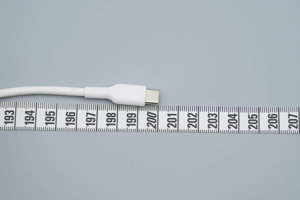
The length is about 200 cm (78.74 inches).
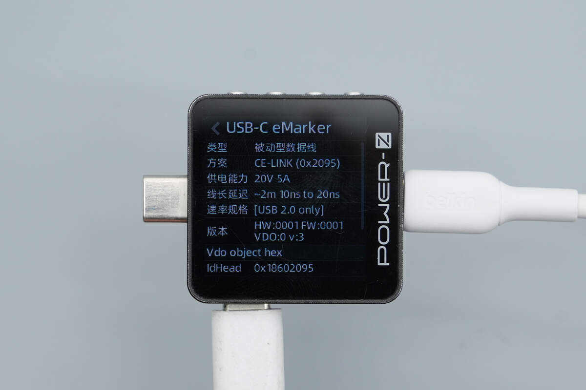
ChargerLAB POWER-Z KM003C shows it has an E-Marker chip, supports power delivery up to 20V5A, and offers data transfer capability compliant with the USB 2.0 standard.
The casing is made of white recycled plastic with a matte finish, featuring a clean and minimalist design style.

The front side features the Belkin logo.
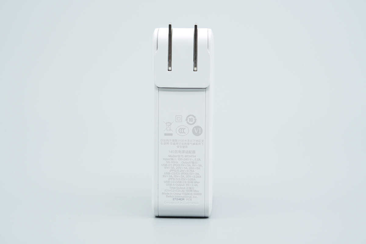
The input side of the casing is printed with the specification information.
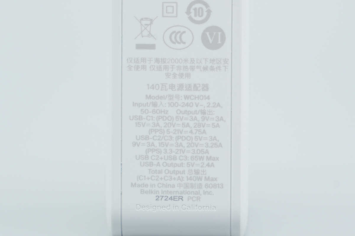
Model: WCH014
Input: 100–240V~ 50/60Hz 2.2A
Output:
USB-C1: PDO 5V 3A, 9V 3A, 15V 3A, 20V 5A, 28V 5A; PPS 5–21V 4.75A
USB-C2/C3: PDO 5V 3A, 9V 3A, 15V 3A, 20V 3.25A; PPS 3.3–21V 3.05A
USB-C2 + USB-C3: 65W Max
USB-A: 5V 2.4A
Total output (C1 + C2 + C3 + A): 140W Max
The charger has obtained CCC certification and Level VI energy efficiency certification.
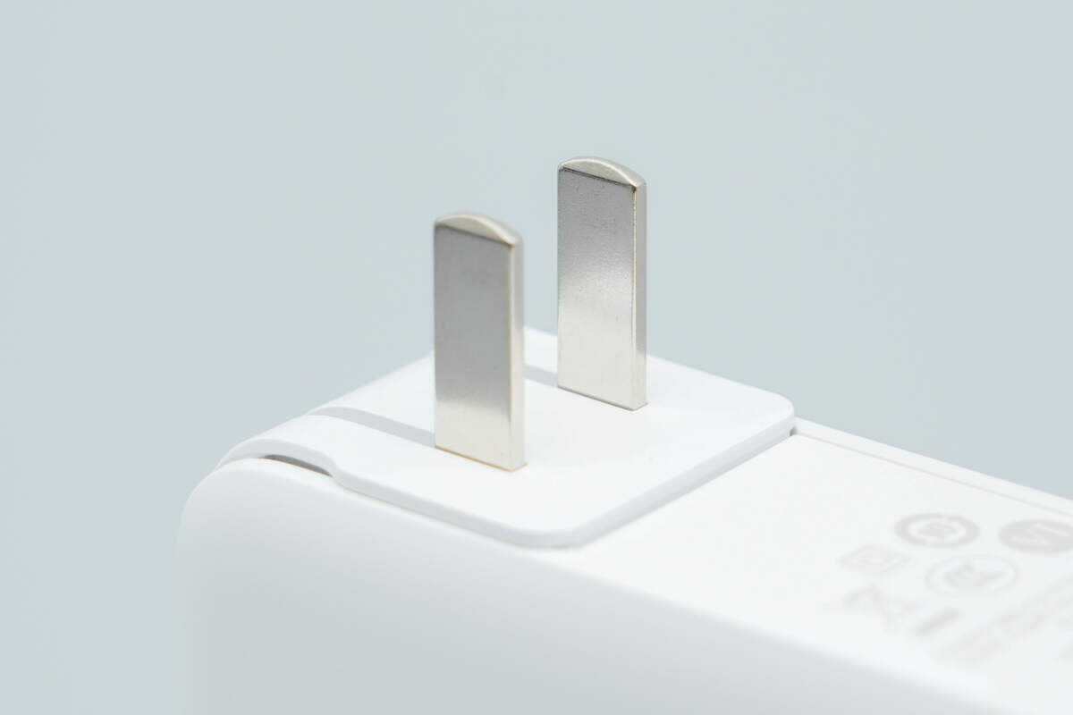
It features foldable plug pins.
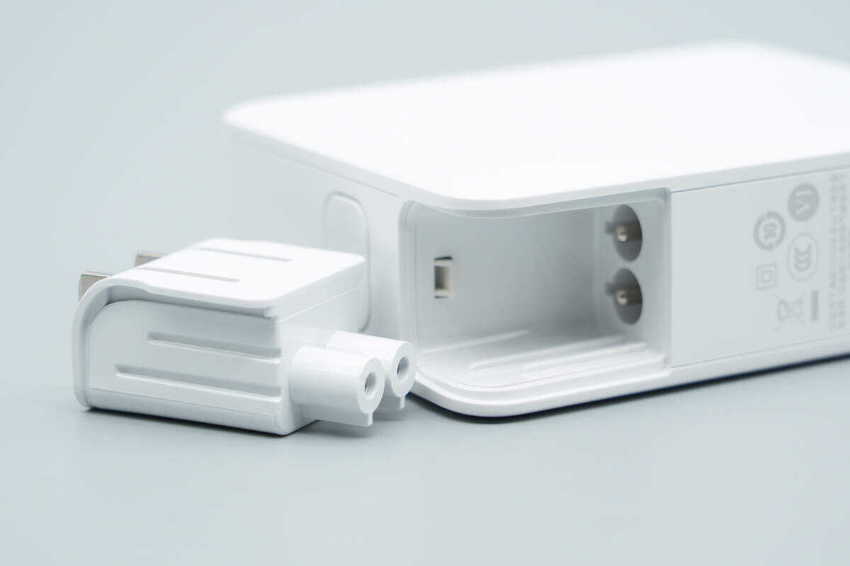
The plug uses a detachable modular design with a locking mechanism to prevent accidental detachment. The interchangeable plugs allow compatibility with different countries and regions.
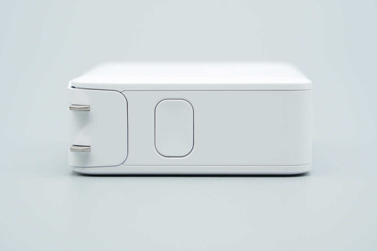
This is the release button for the plug module.
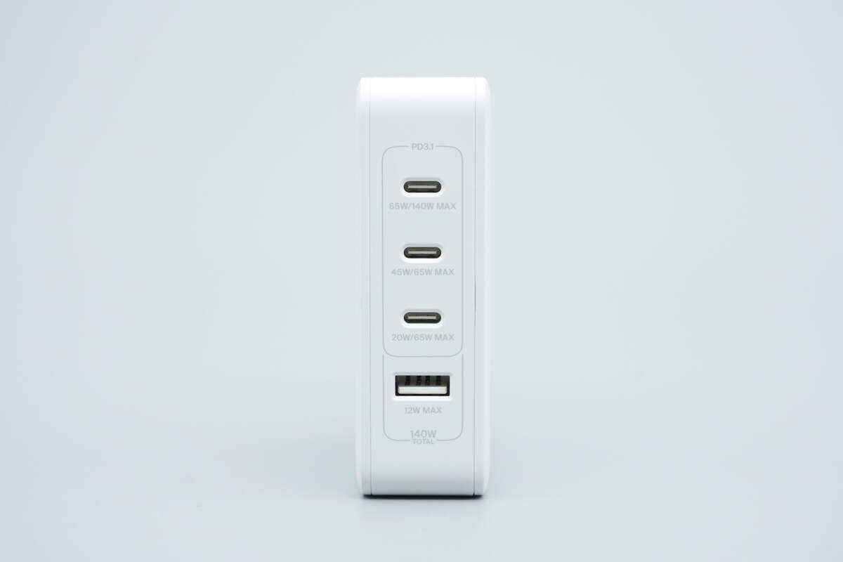
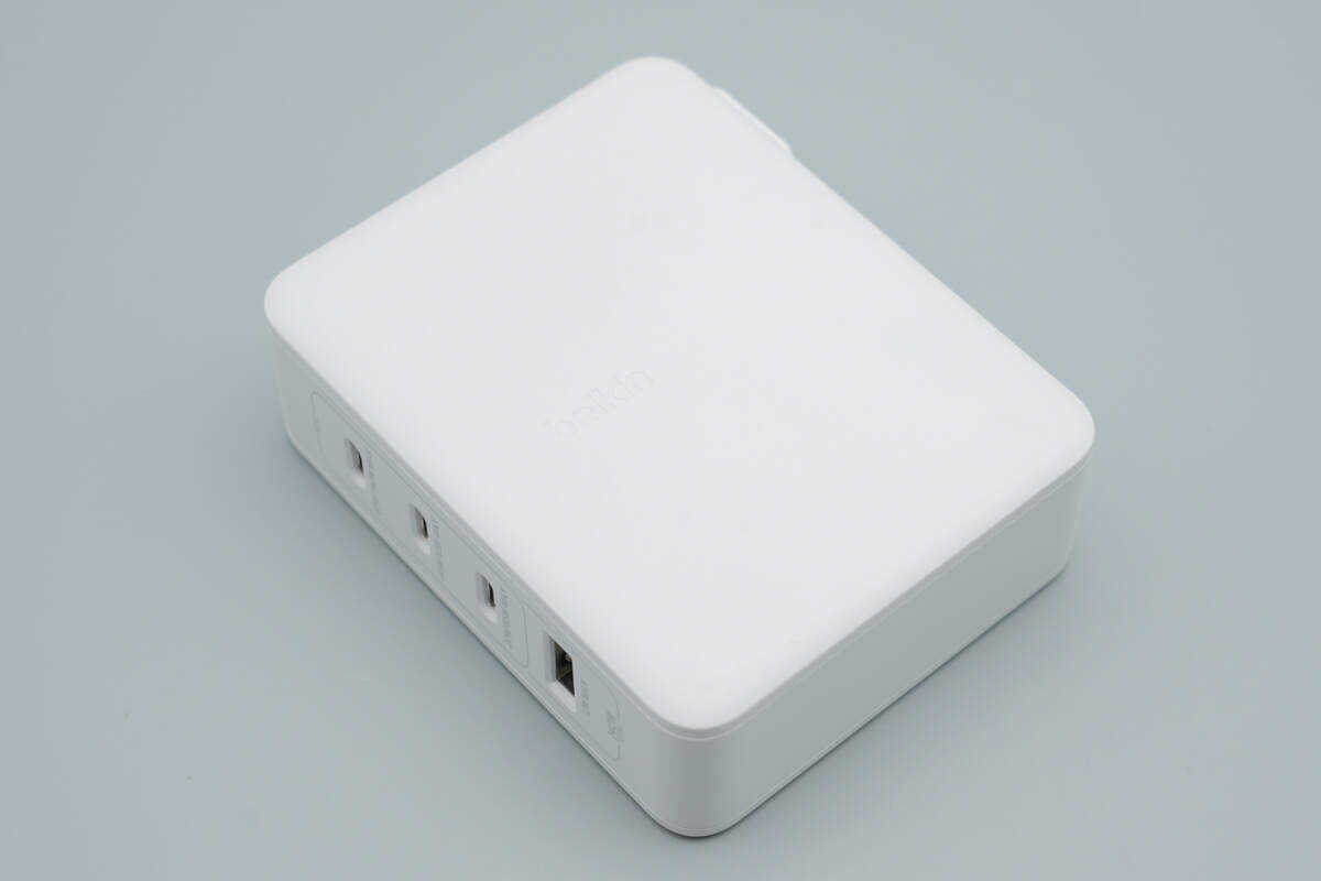
The output side is equipped with three USB-C ports and one USB-A port.
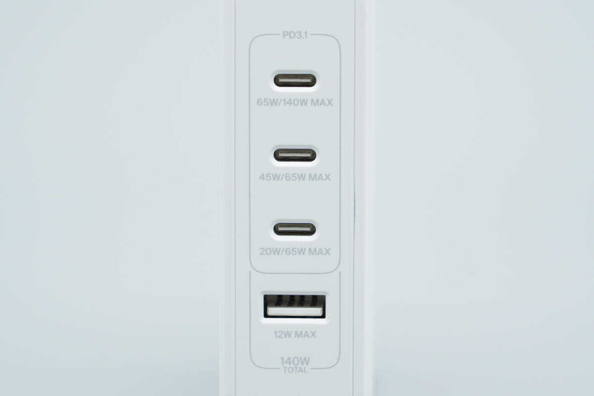
Next to the ports, the power ratings for single-port and multi-port outputs are printed.

The length of the charger is about 95.97 mm (3.78 inches).
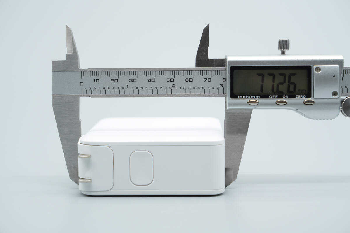
The width is about 77.26 mm (3.042 inches).
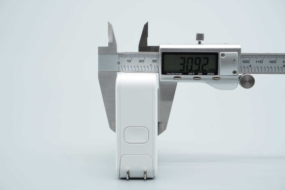
The thickness is about 30.92 mm (1.22 inches).
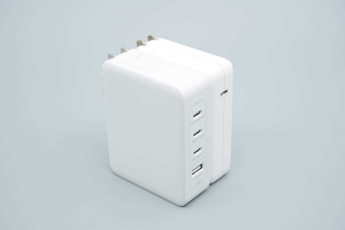
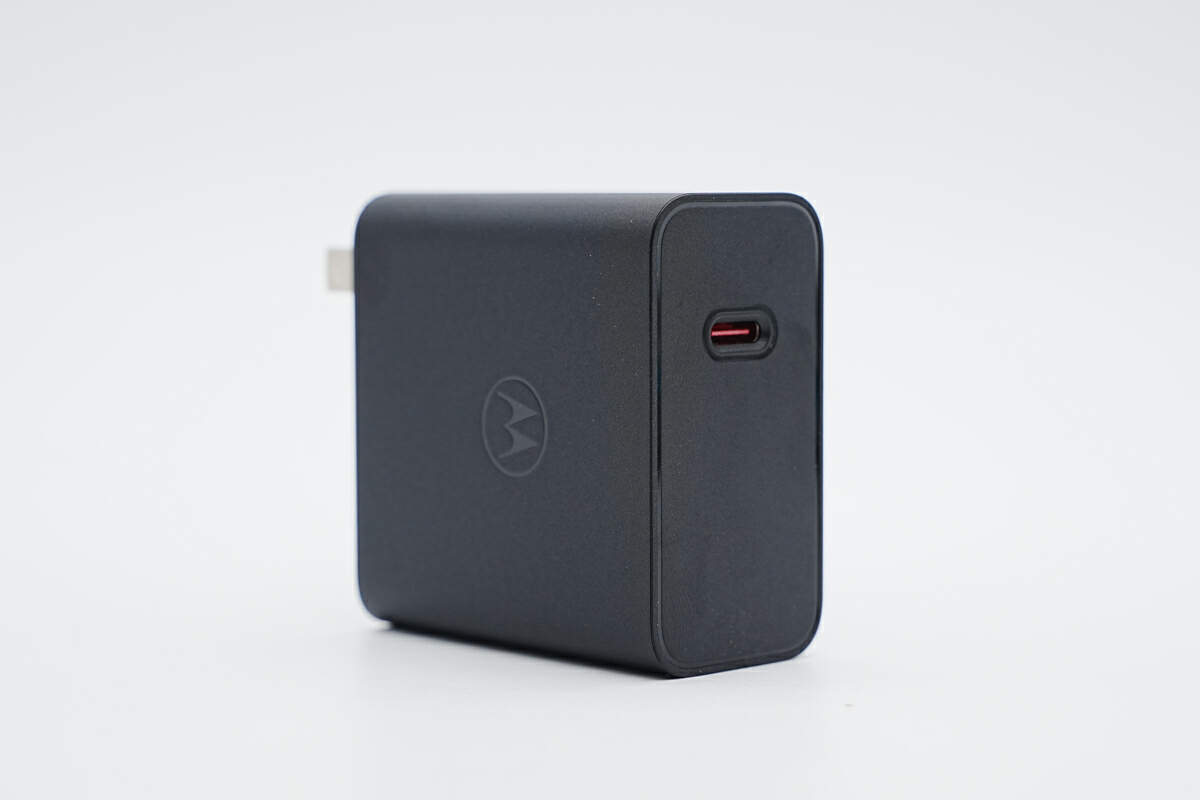
This Belkin charger is slightly larger than Apple 140W GaN charger.

That's how big it is in the hand.
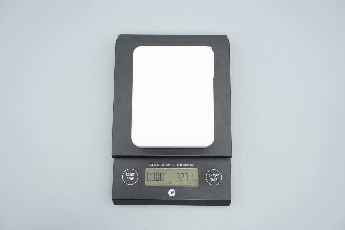
The weight is about 327 g (11.53 oz).
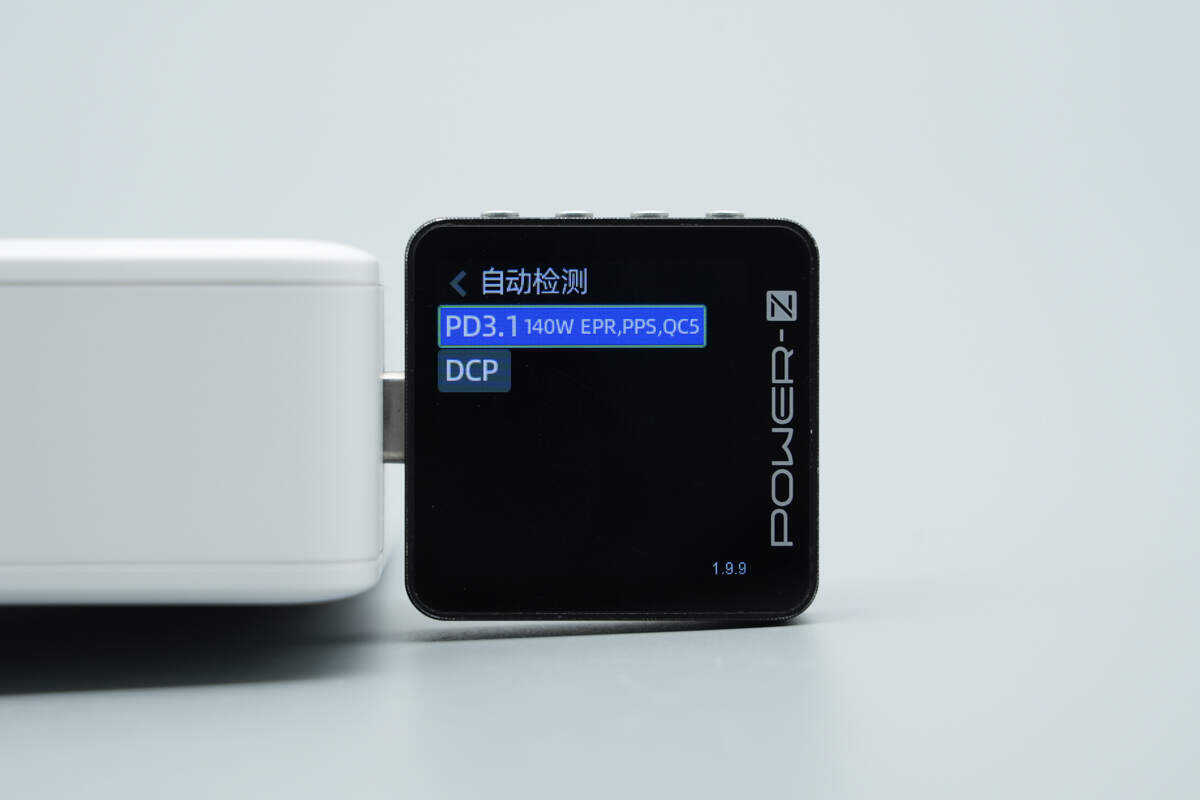
ChargerLAB POWER-Z KM003C shows that the USB-C1 supports PD3.1, PPS, QC, and DCP charging protocols.

It features five fixed PDOs: 5V3A, 9V3A, 15V3A, 20V5A, and 28V5A, as well as a set of PPS, which is 5-21V5A.
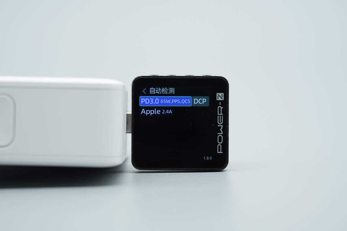
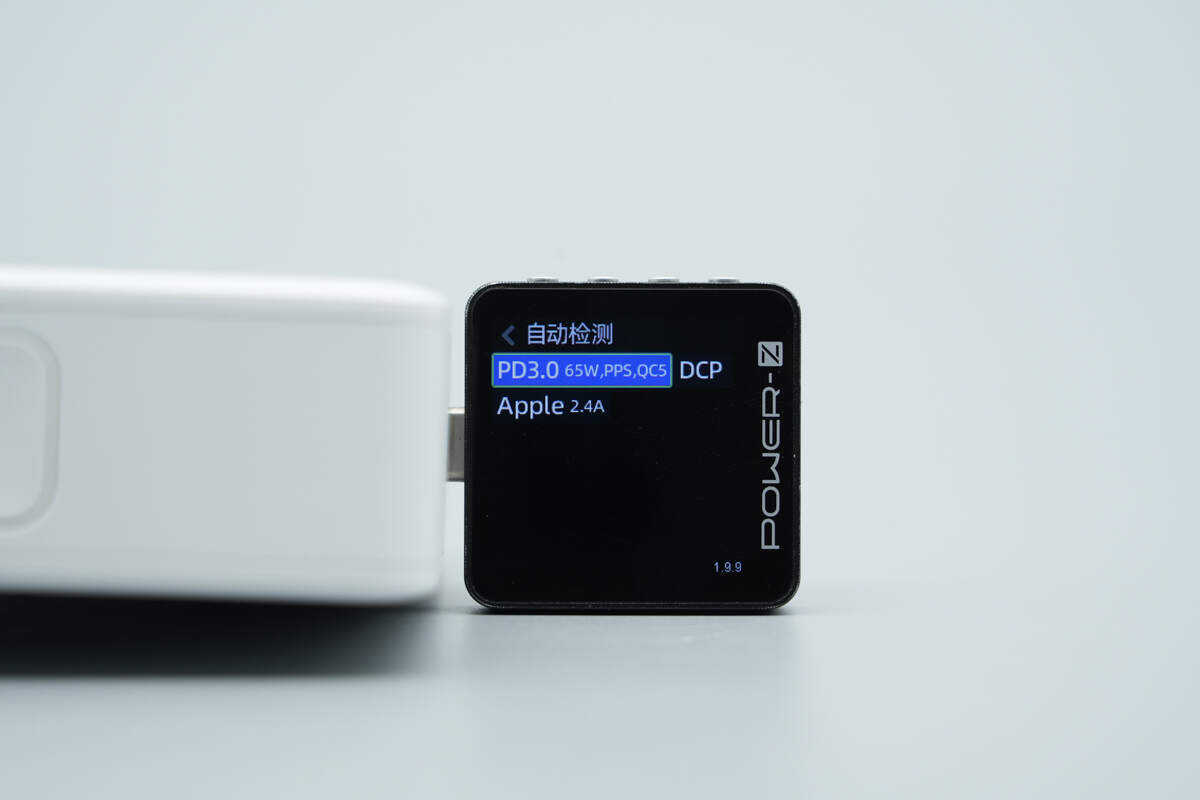
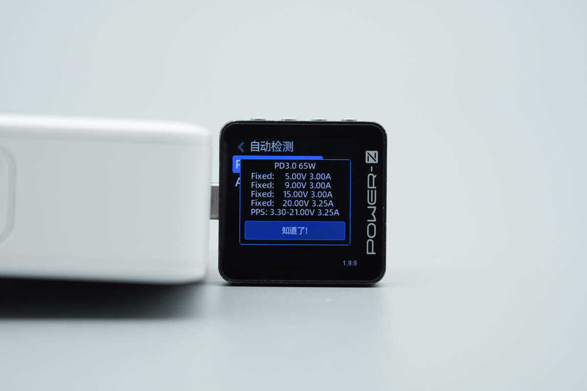
The USB-C2 port supports PD3.0, PPS, DCP, and Apple 2.4A protocols.
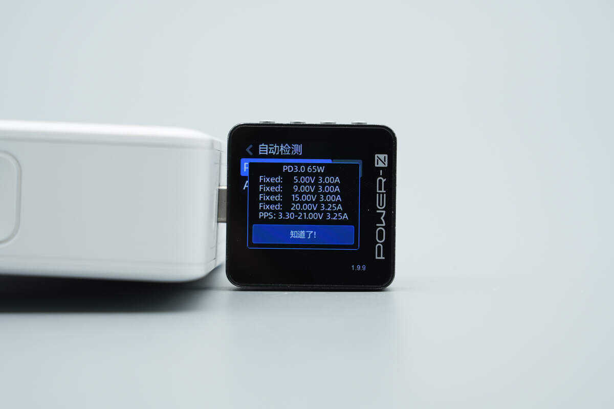
And it has four fixed PDOs of 5V3A, 9V3A, 15V3A, and 20V3.25A. It has one set of PPS, which is 3.3-21V3.25A.
The USB-C3 port supports the same protocols as the USB-C2 port.
The PDO reports are also identical.
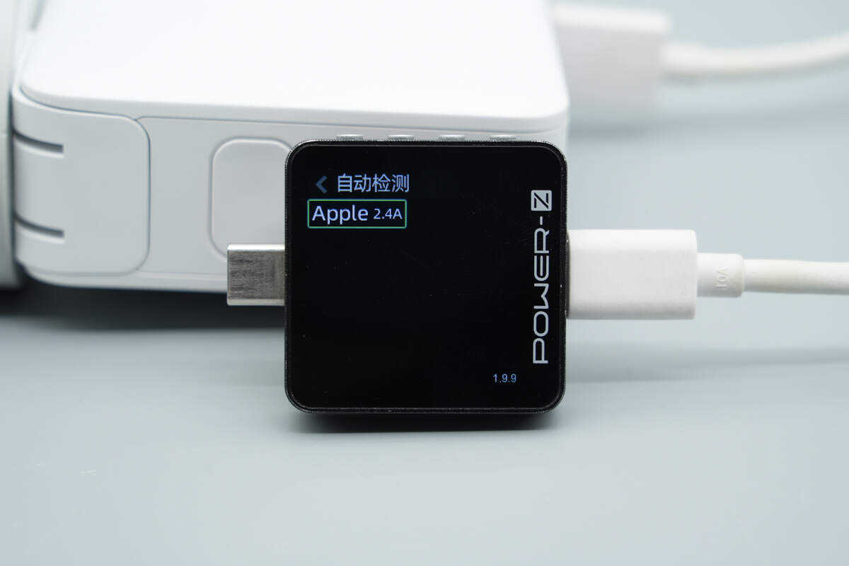
The USB-A port supports the Apple 2.4A protocol.
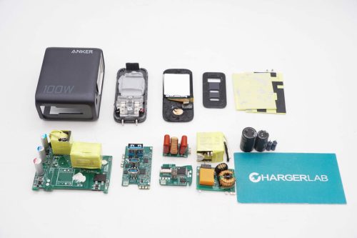
Teardown
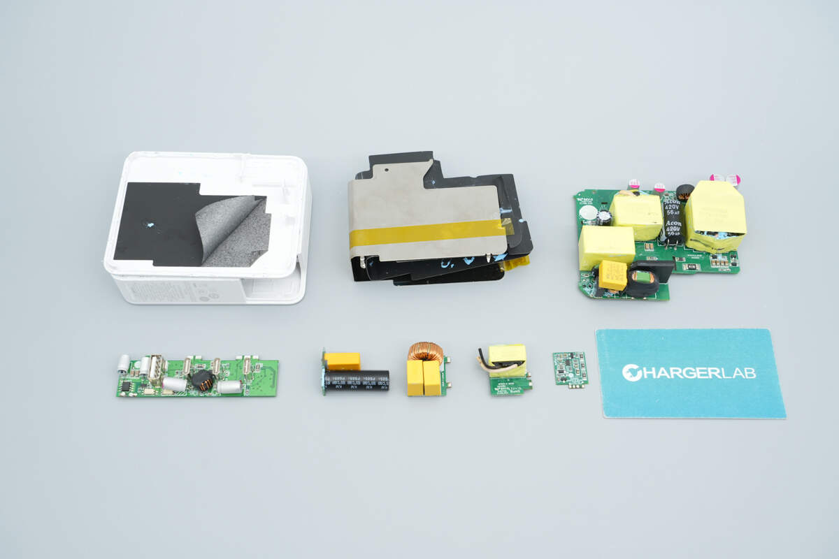
Next, let's take it apart to see its internal components and structure.
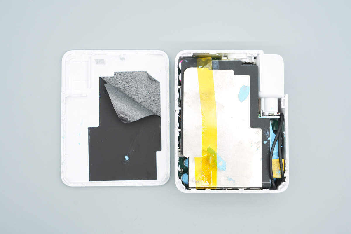
Upon opening the casing, a graphite thermal pad is attached to the inner side of the shell.
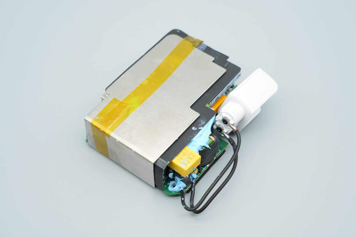
Remove the PCBA module. The module is encased in a U-shaped metal heat sink and secured with tape.
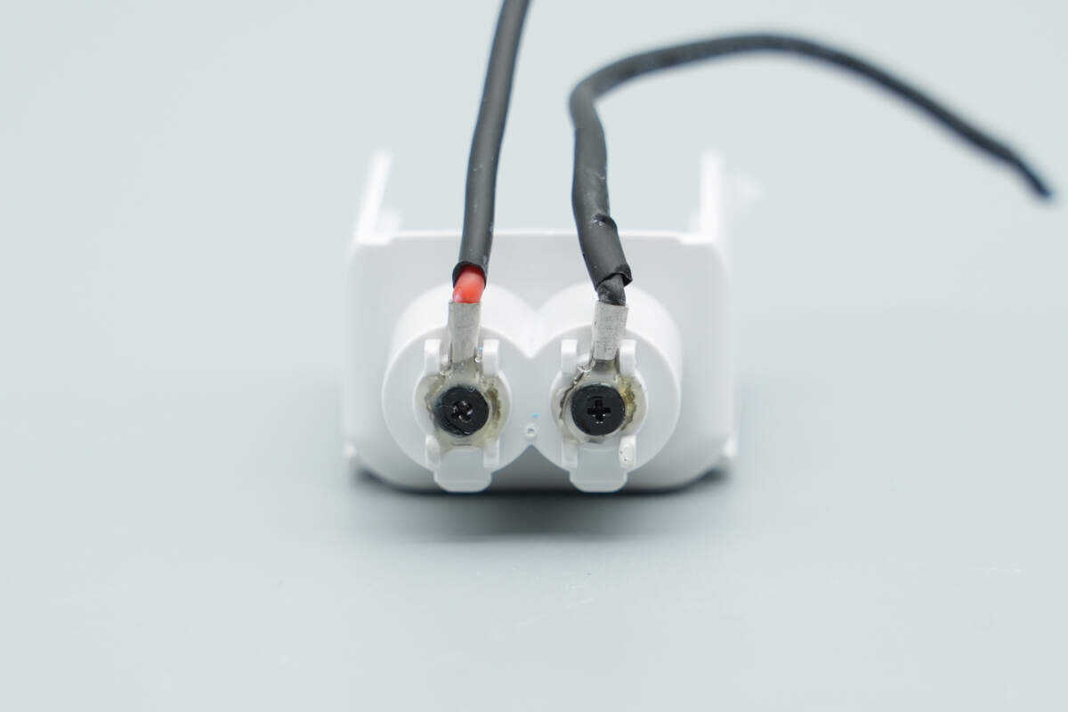
One end of the socket wires is secured with screws and treated with adhesive for added stability.
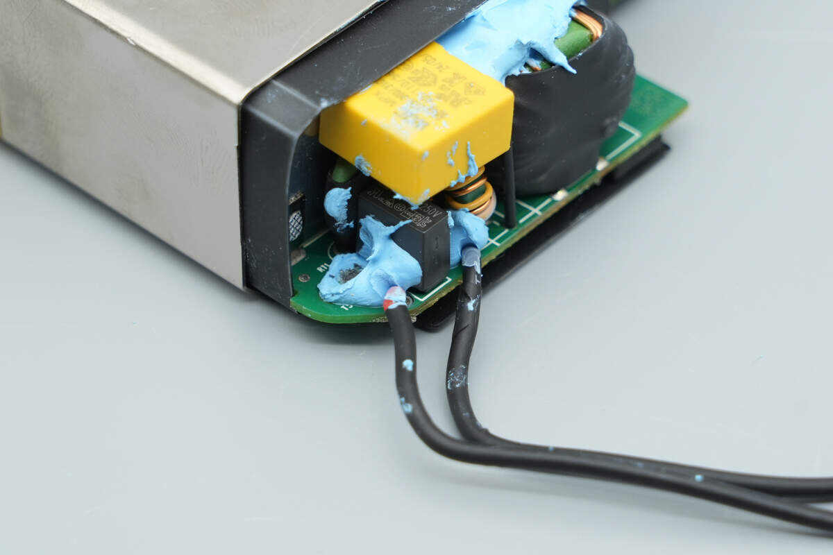
The other end is soldered to the PCBA module, with thermal paste applied at the soldered joints.
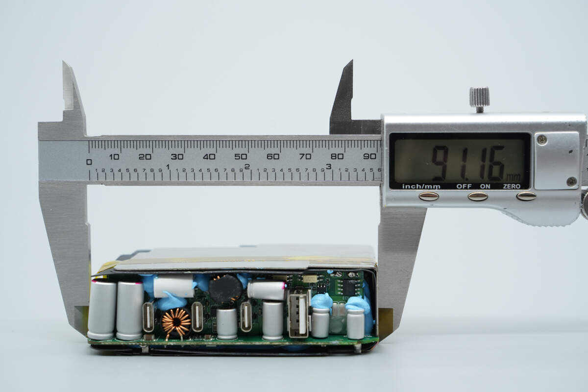
The length of the PCBA module is about 91.16 mm (3.59 inches).
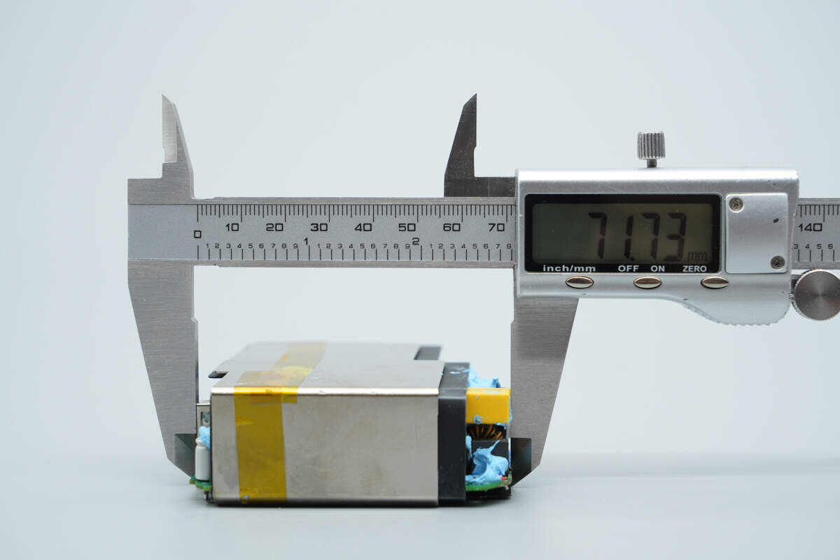
The width is about 71.73 mm (2.82 inches).
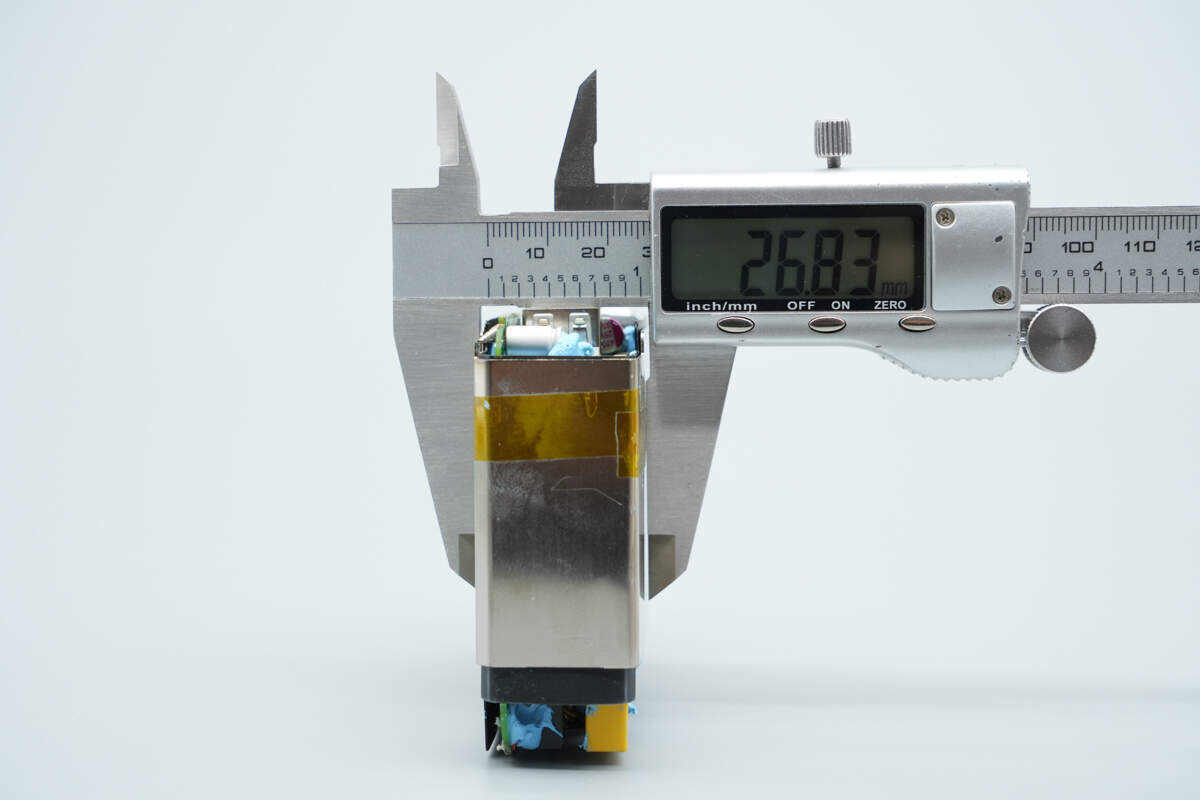
The thickness is about 26.93 mm (1.06 inches).
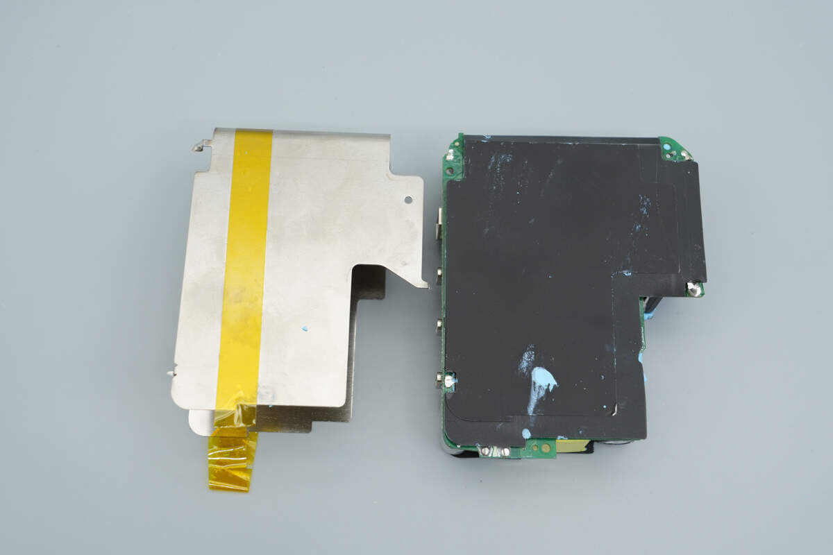
Remove the heat sink. A Mylar sheet is installed on the inner side for insulation.
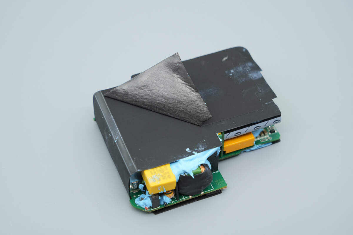
A graphite thermal pad is also attached to the Mylar sheet.
Remove the Mylar sheet. The gaps between the components on the front of the PCBA module are filled with thermal paste.
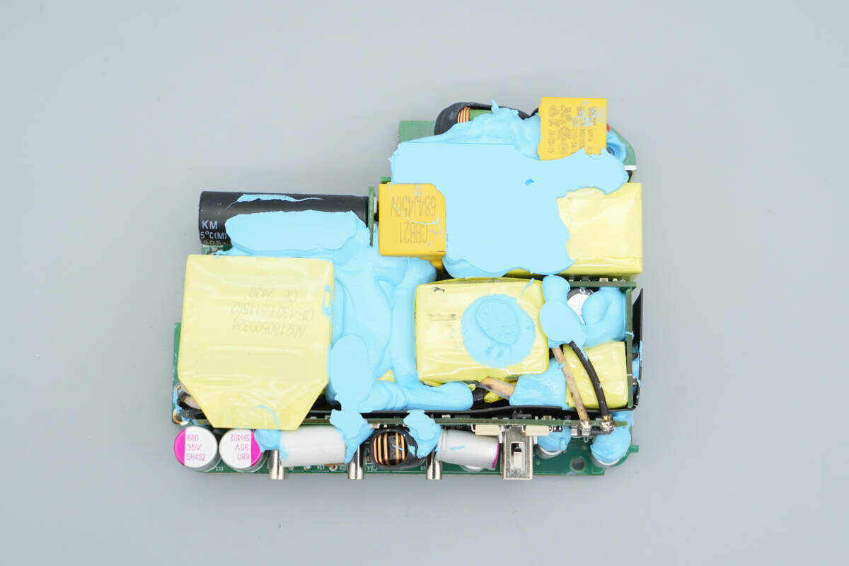
The back side is also filled with thermal paste.
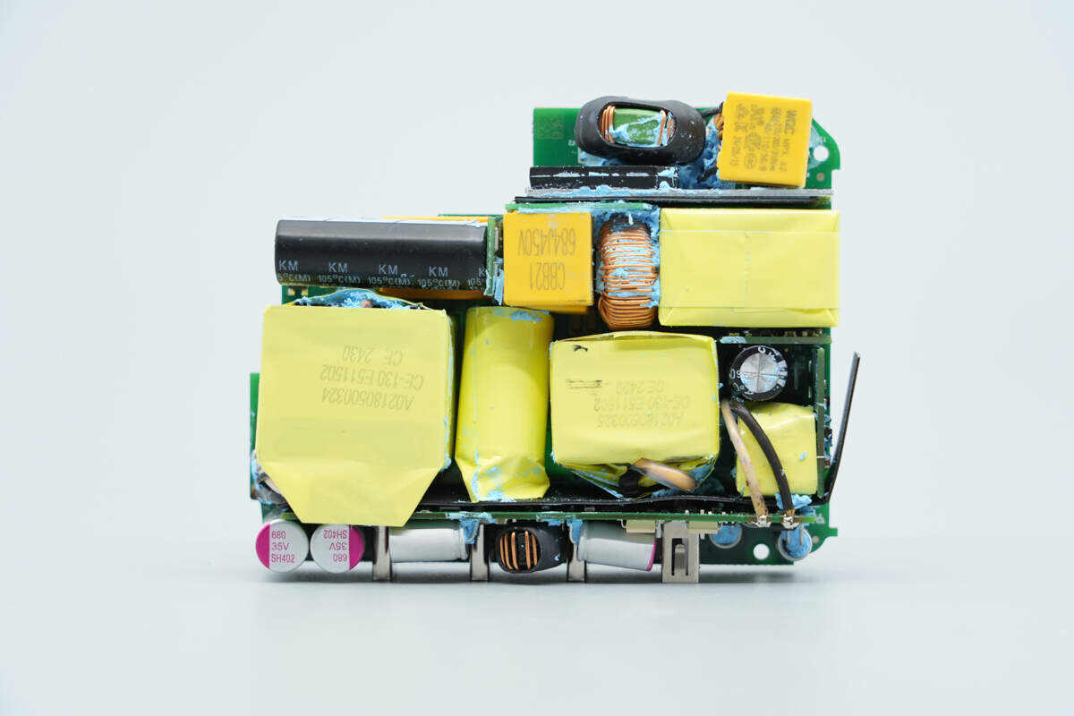
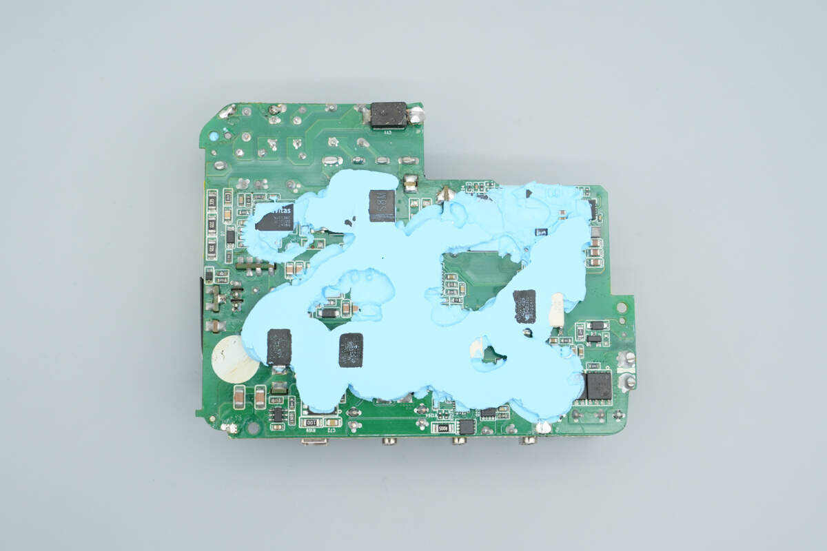
Clean off the thermal paste. The front of the PCBA has three transformers, indicating that this charger uses a three-channel switching power supply design.
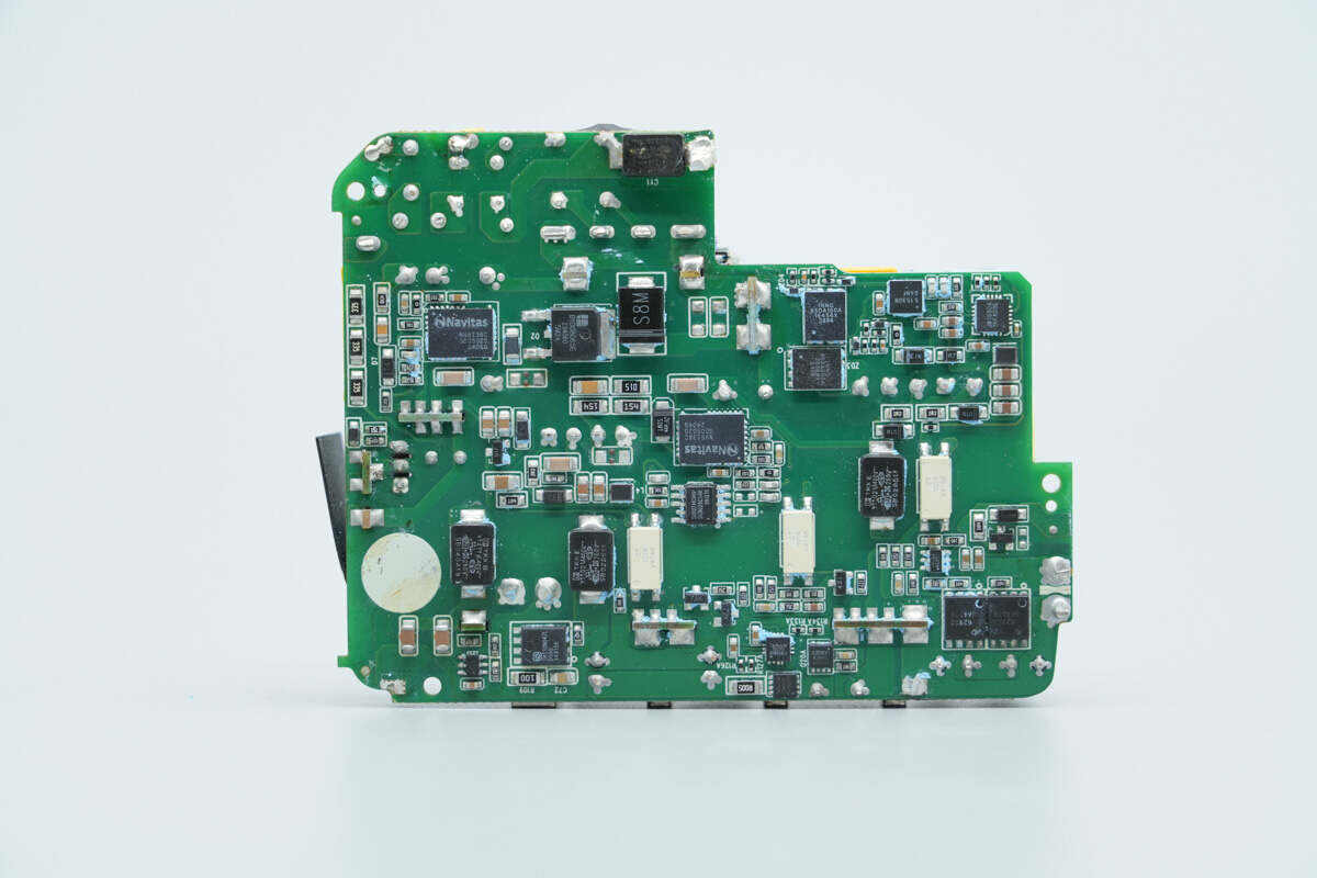
On the back side, there is a PFC boost controller, MOSFETs, and rectifiers, along with primary and secondary controllers, MOSFETs, and synchronous rectifiers for two of the switching power supply channels. There is also a synchronous buck controller and buck MOSFETs dedicated to the secondary step-down output for USB-C1.
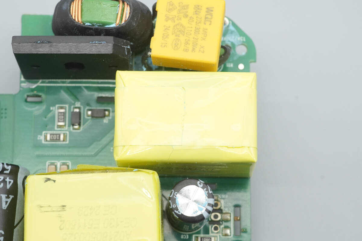
At the front end of the module, there is a time-delay fuse, common mode chokes, a safety X2 capacitor, a bridge rectifier, and a filter PCB.
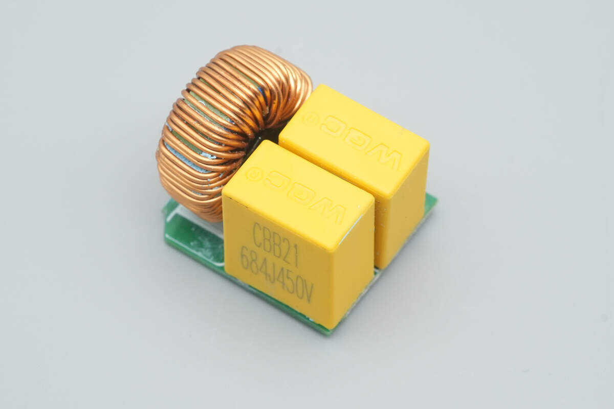
Remove the filter PCB. The front side reveals two film capacitors and a filter inductor.
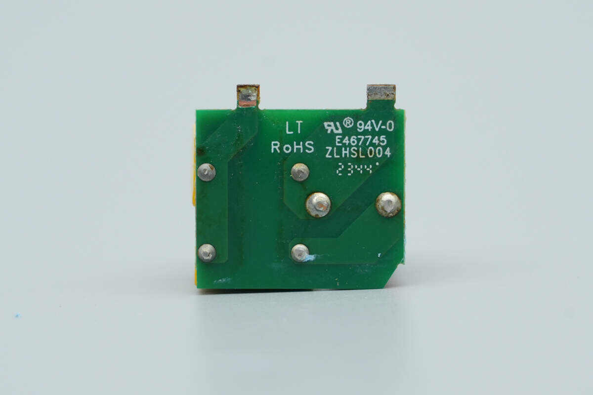
The back side has no components.
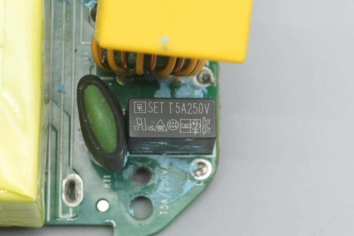
The time-delay fuse is from Chevron, rated at 5A 250V.
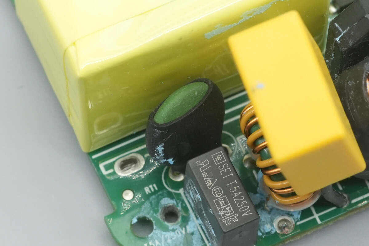
The NTC thermistor is used to suppress inrush current, and it is insulated with a heat-shrink tube for protection.
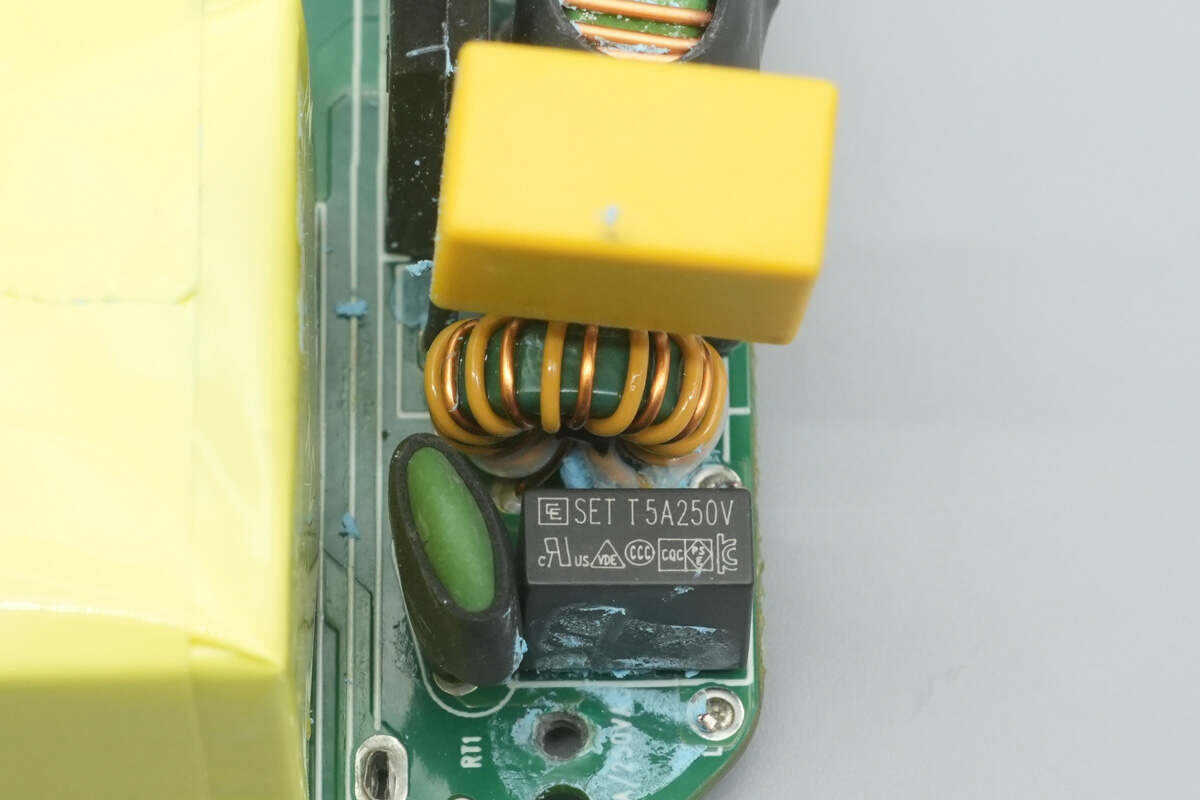
The common mode choke is dual-wound and used to filter EMI interference.
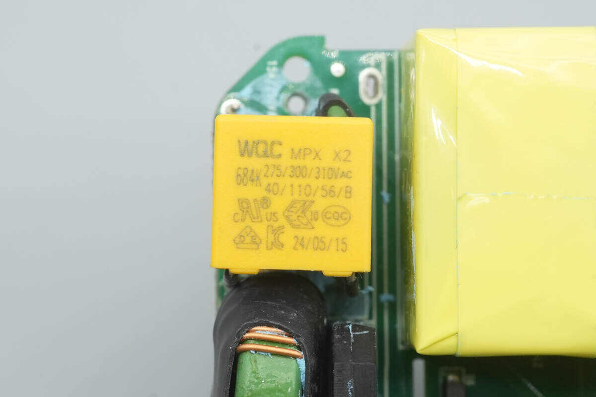
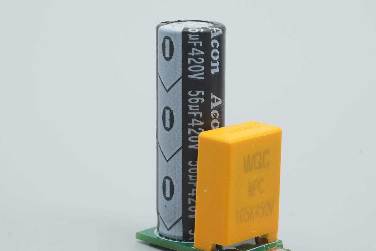
The safety X2 capacitor is from WQC, with a capacitance of 0.68 µF.
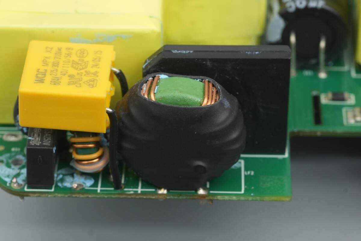
Another common-mode choke is covered with a heat-shrink tube for insulation and protection.
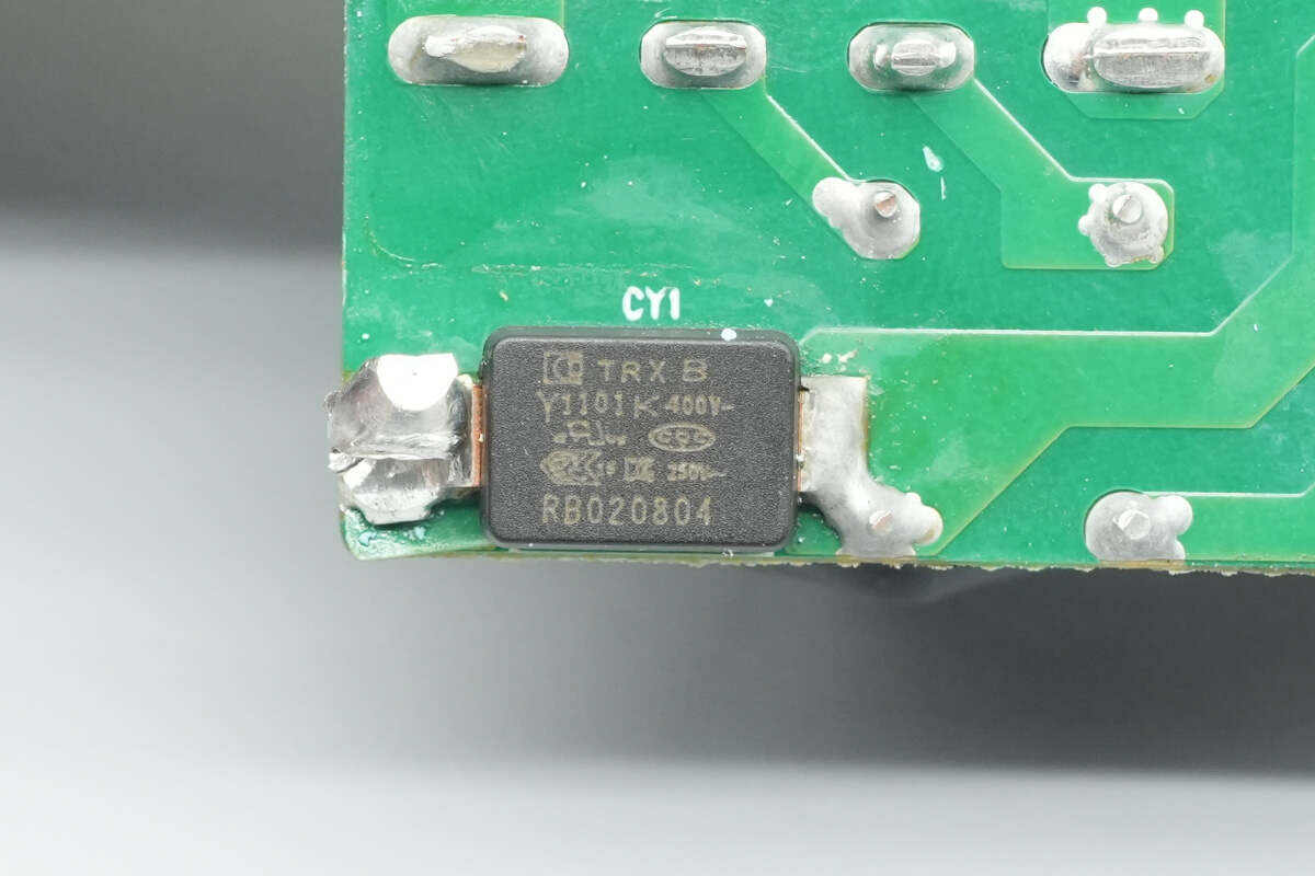
The SMD Y capacitor is from TRX, part number TMY1101K. Its compact size and light weight make it well-suited for high-density power products such as GaN fast chargers.
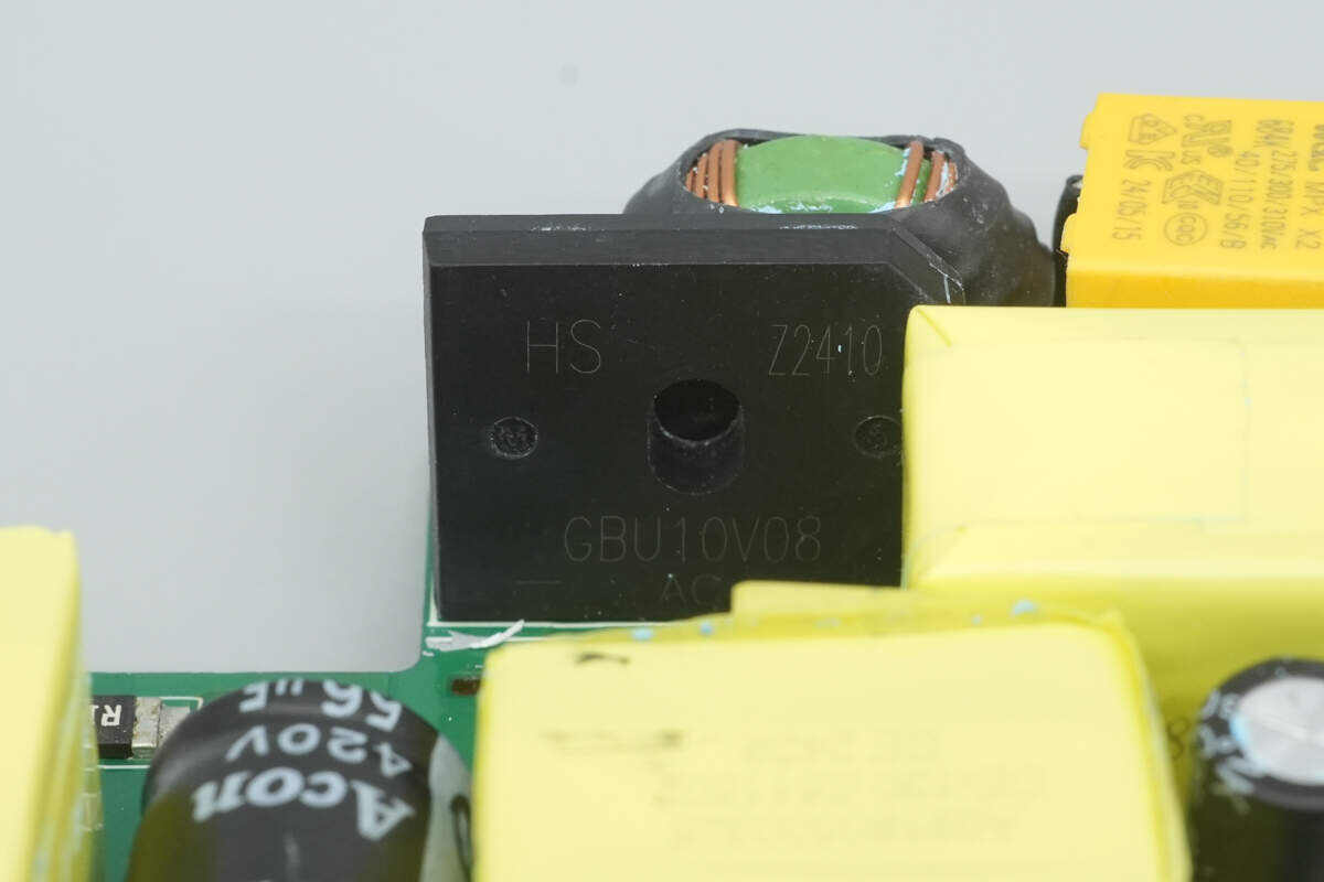
The bridge rectifier is model GBU10V08, rated at 10A 800V.
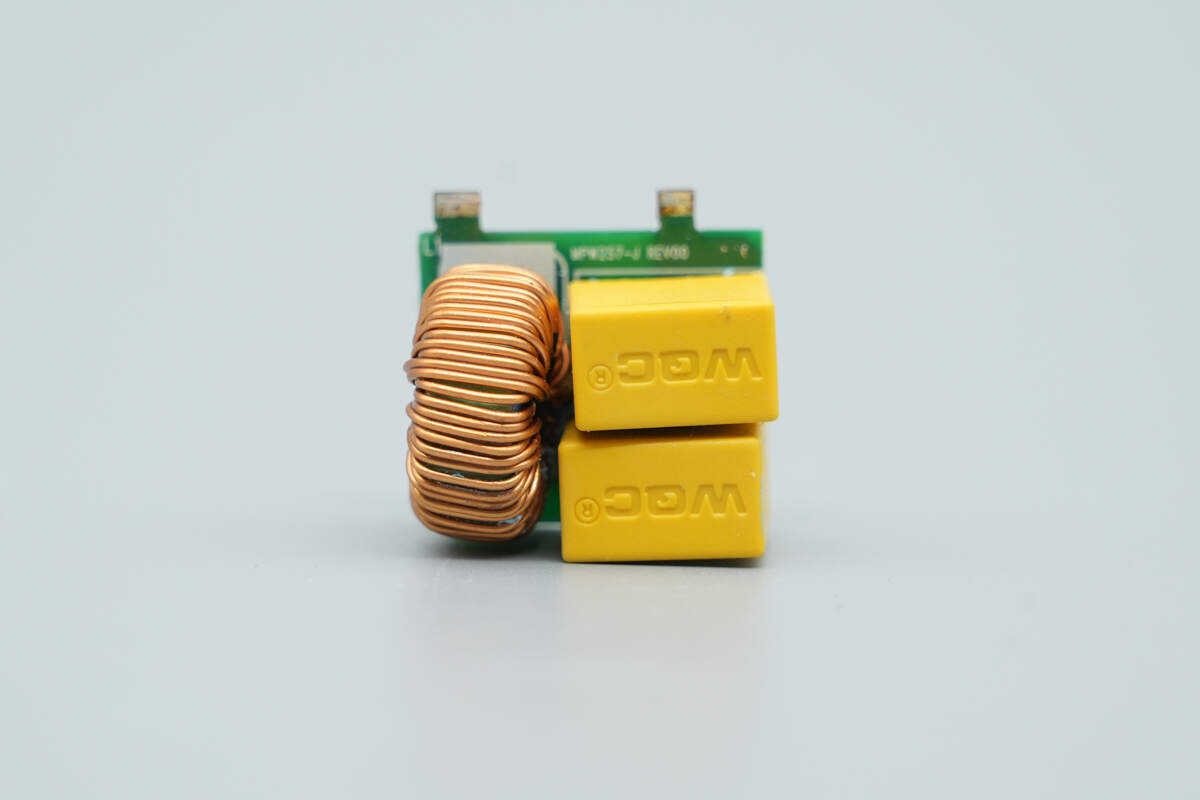
The two film capacitors are from WQC and share the same part number.
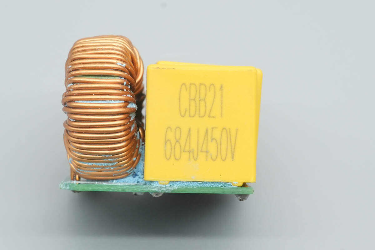
The CBB21 film capacitors are rated at 0.68 μF 450 V.
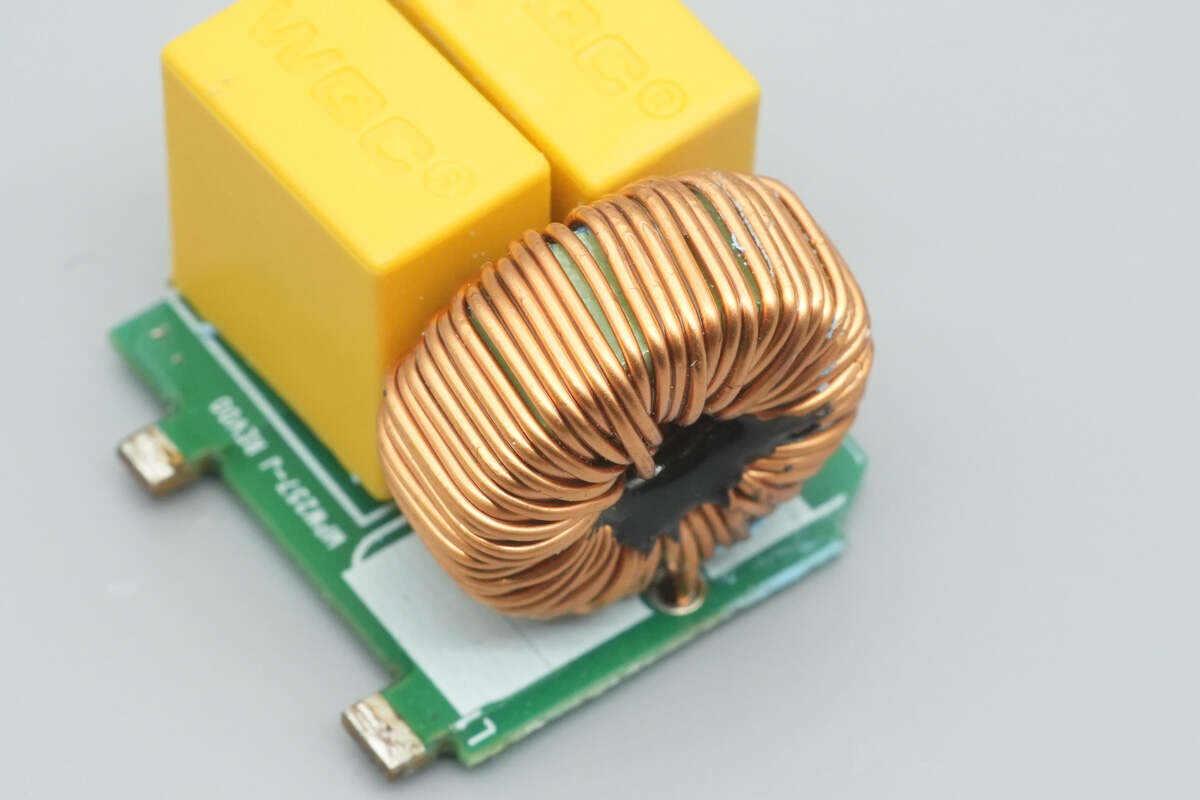
The toroidal filter inductor is dual-wound in parallel.
Remove the PFC control PCB. The front side reveals the PFC controller and its peripheral components.
The back side has no components.
The PFC boost controller is from Onsemi, model NCP1622. It is an enhanced critical-mode boost PFC controller featuring valley-frequency skipping, improved transient response, and higher conversion efficiency. It requires minimal external components and comes in a TOSP-6 package.
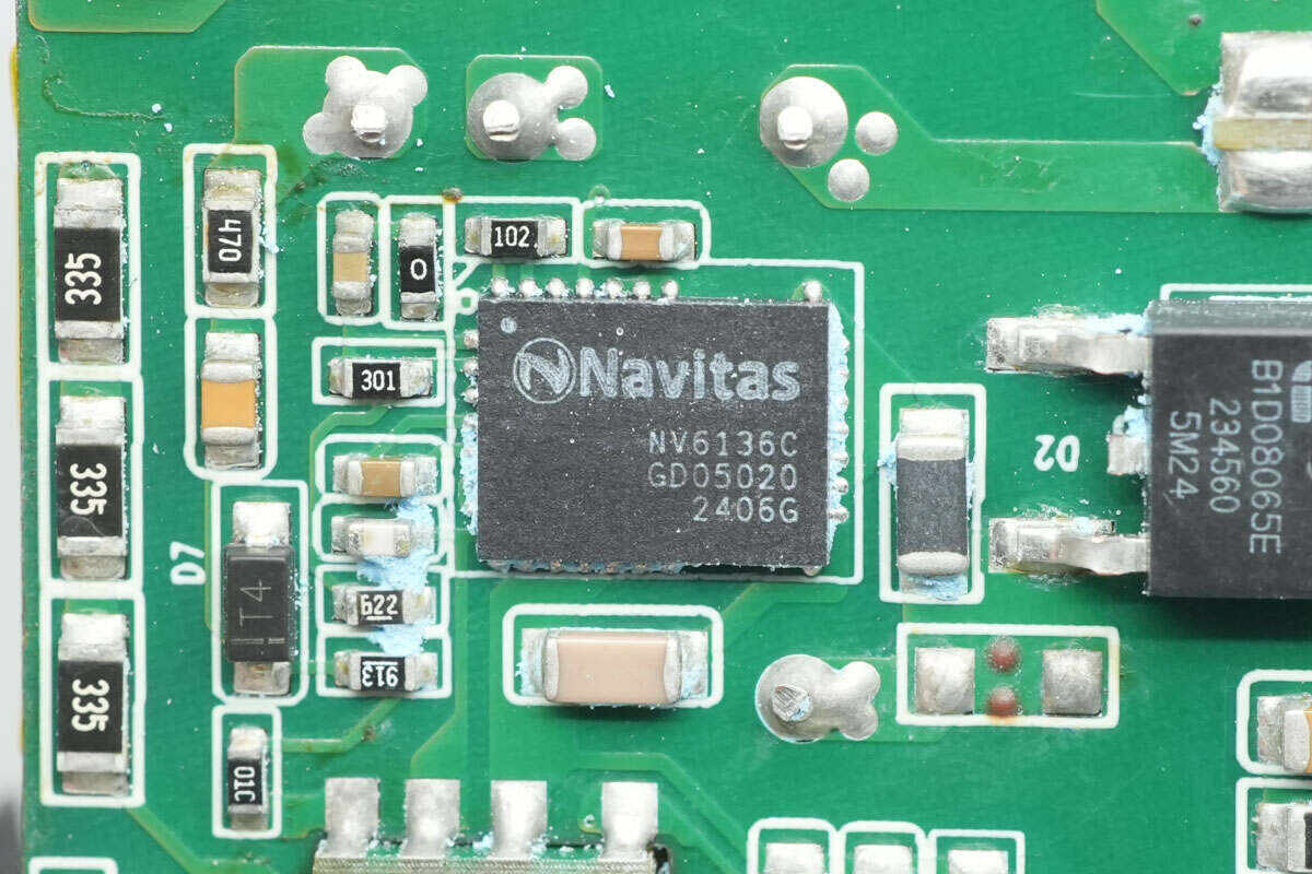
The PFC MOSFET is from Navitas, model NV6136C. It is a highly integrated GaN power device with a built-in driver and high-precision lossless current-sensing circuit, eliminating the losses associated with sense resistors. The NV6136C features a 170 mΩ on-resistance, a 700 V GaN switch, supports up to 2 MHz switching frequency, and comes in a compact 6×8 mm QFN package, saving PCB space.
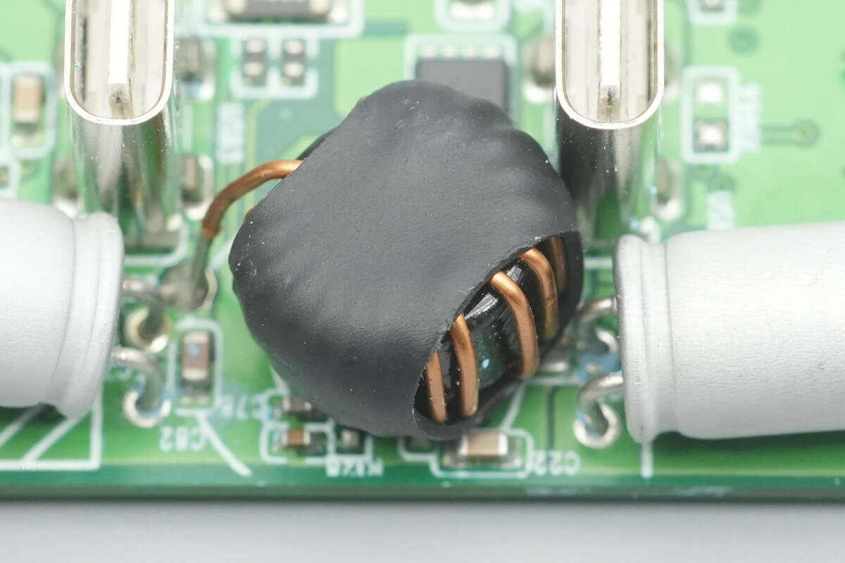
The PFC boost inductor is wrapped with tape.
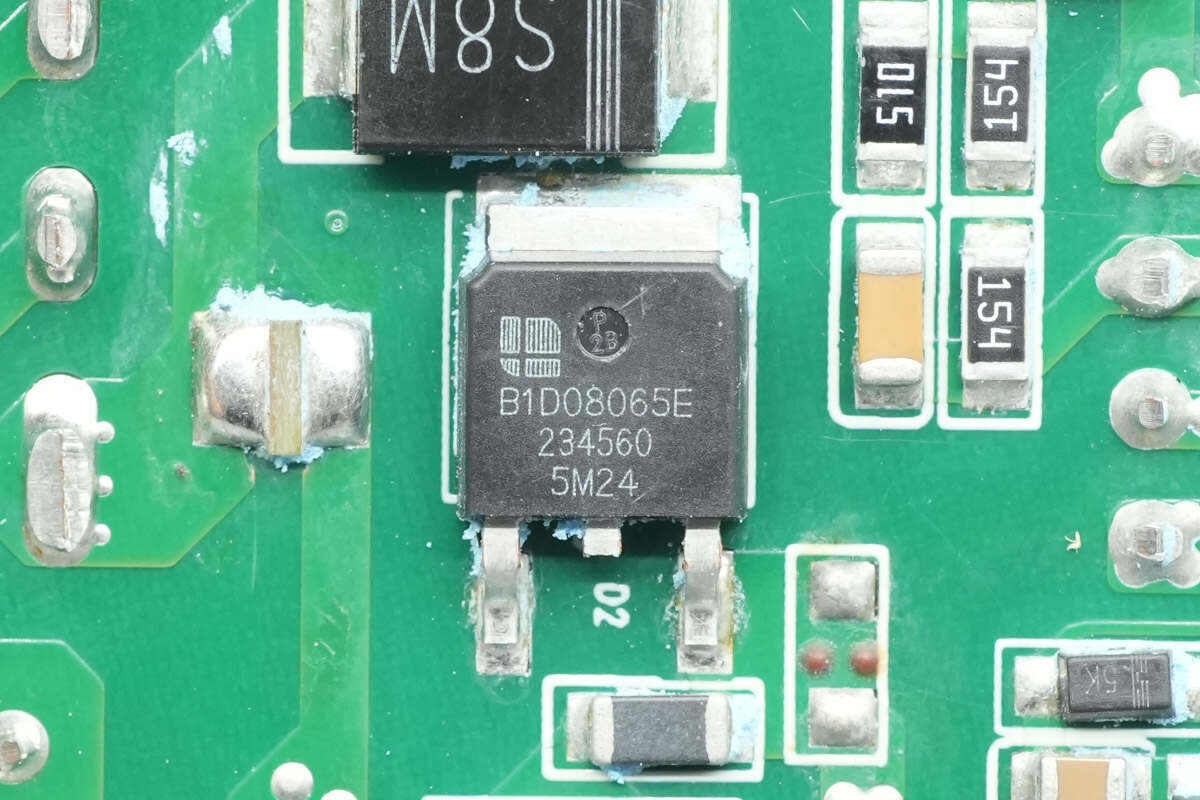
The PFC rectifier is from BASiC, model B1D08065E. It is a 650 V SiC diode with an 8 A operating current at 155 °C, packaged in TO-252-2.
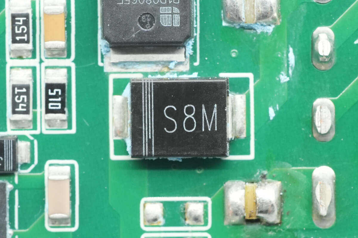
An SMD diode marked S8M is used for bypass purposes.
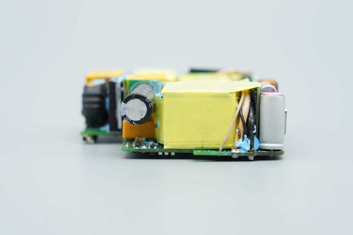
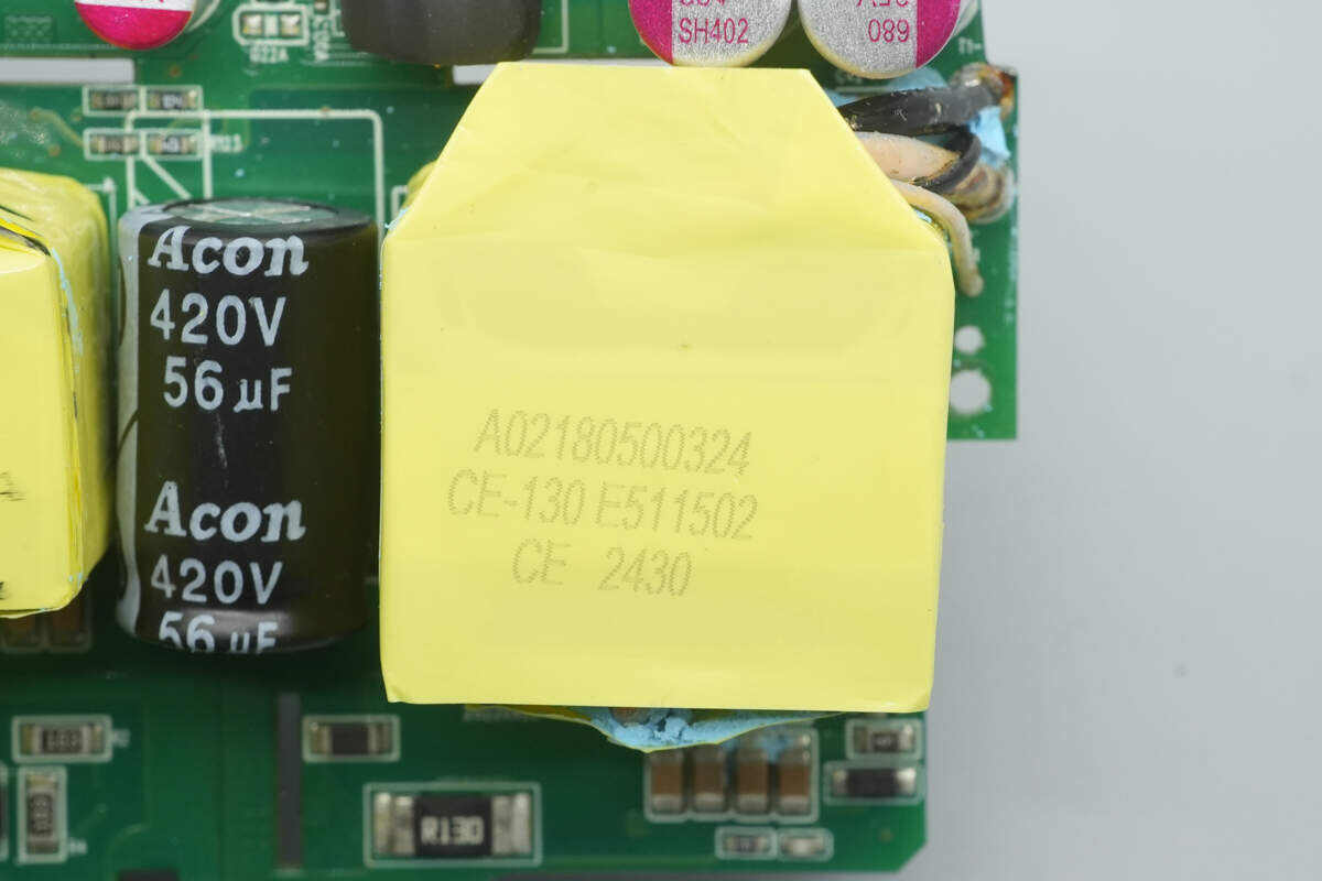
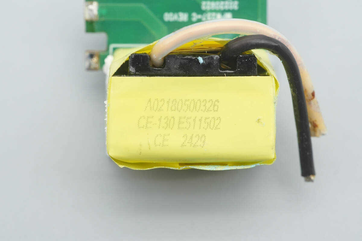
On the other side features a transformer, and a small PCB hosts a film capacitor and a high-voltage filter electrolytic capacitor.
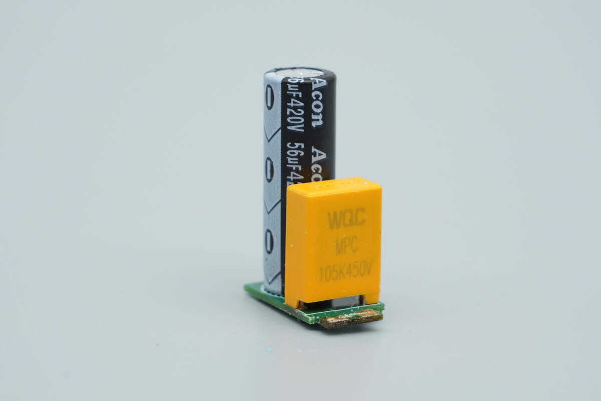
Remove the small PCB holding the two capacitors.
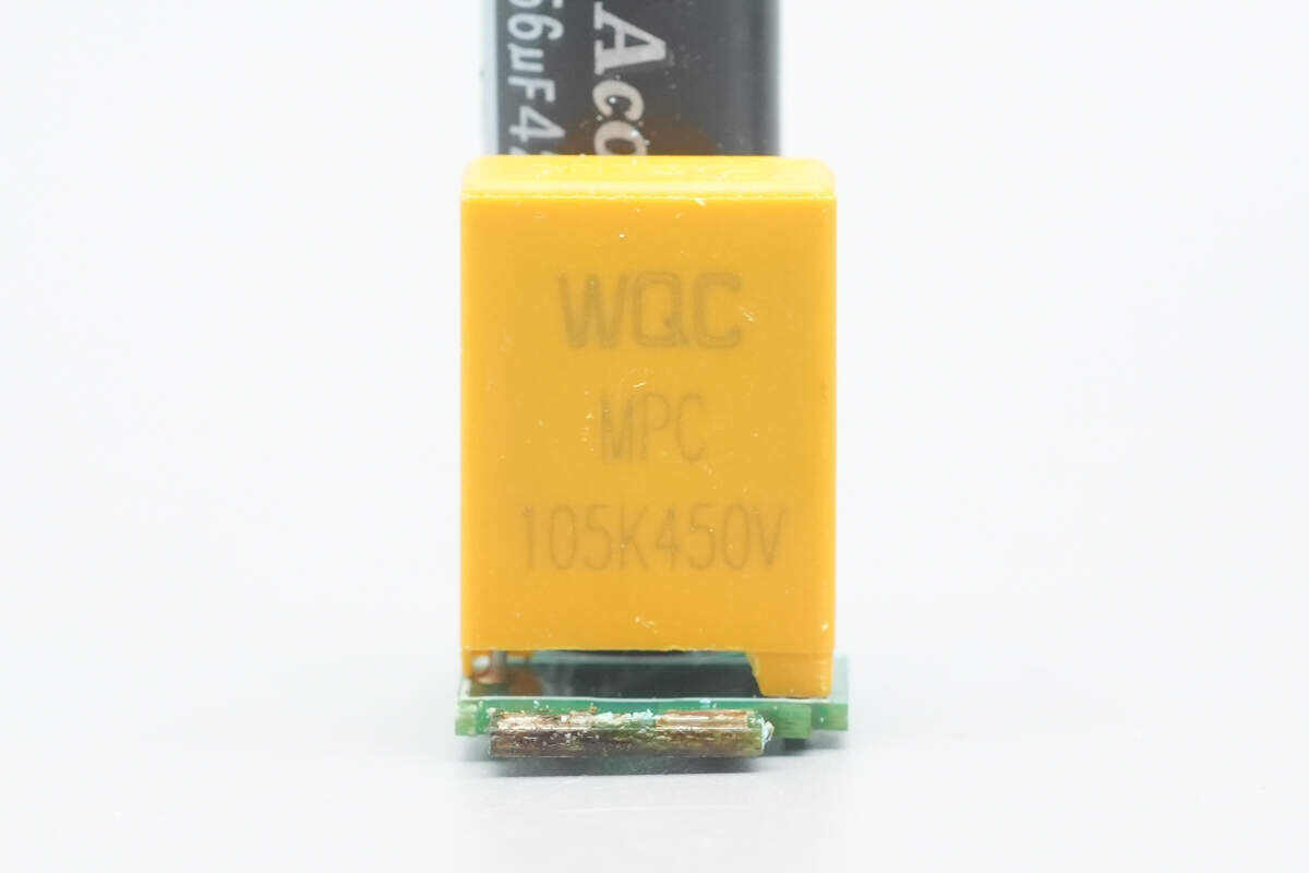
The film capacitor is from WQC, part of the MPC series, rated at 1 μF 450 V.
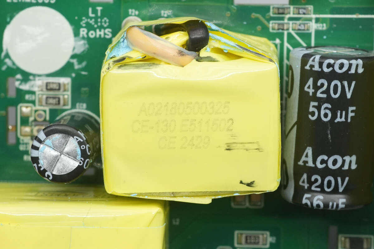
The high-voltage filter electrolytic capacitor is from Acon, rated at 56 μF 420 V.
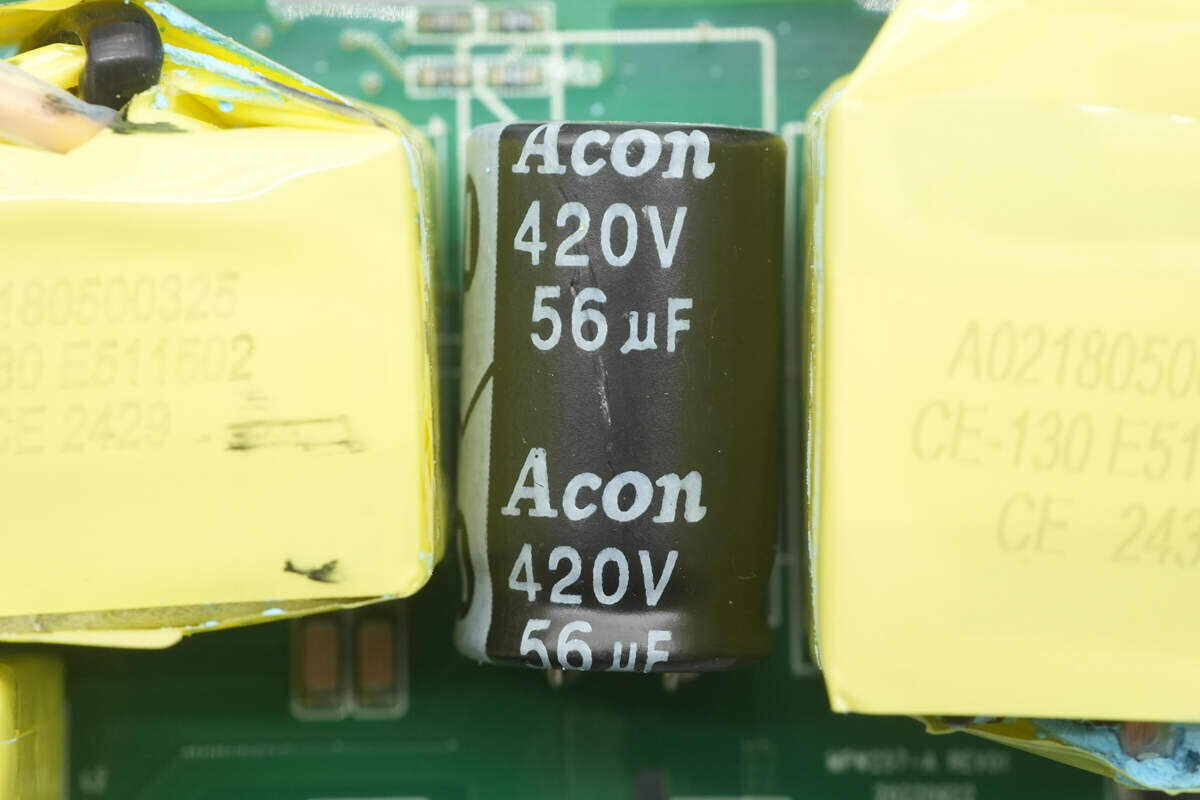
The other high-voltage filter electrolytic capacitor is also from Acon, with the same rating of 56 μF 420 V.
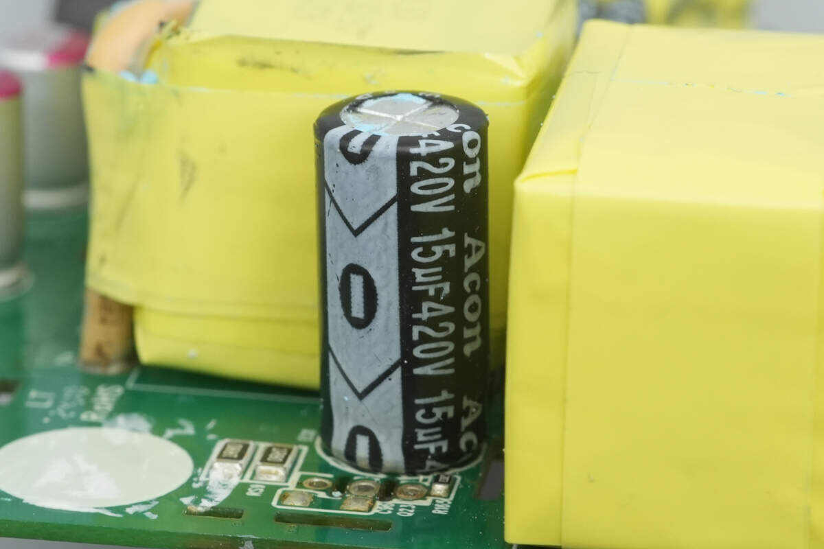
There is also a filter capacitor rated at 15 μF 420 V, bringing the total filter capacitance to 127 μF.
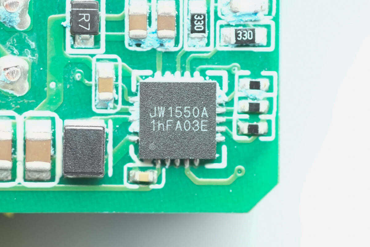
The active-clamp flyback controller is from JOULWATT, model JW1550A. It enables ZVS turn-on to improve efficiency and supports high-frequency applications. The controller also recovers leakage inductance energy for further efficiency gains, incorporates spread-spectrum frequency modulation to enhance EMI performance, and supports X-cap discharge. Its internal boost circuit allows wide-range output operation while minimizing power loss, and the external circuitry is simple, facilitating easy implementation.
Here is the information about JOULWATT JW1550A.
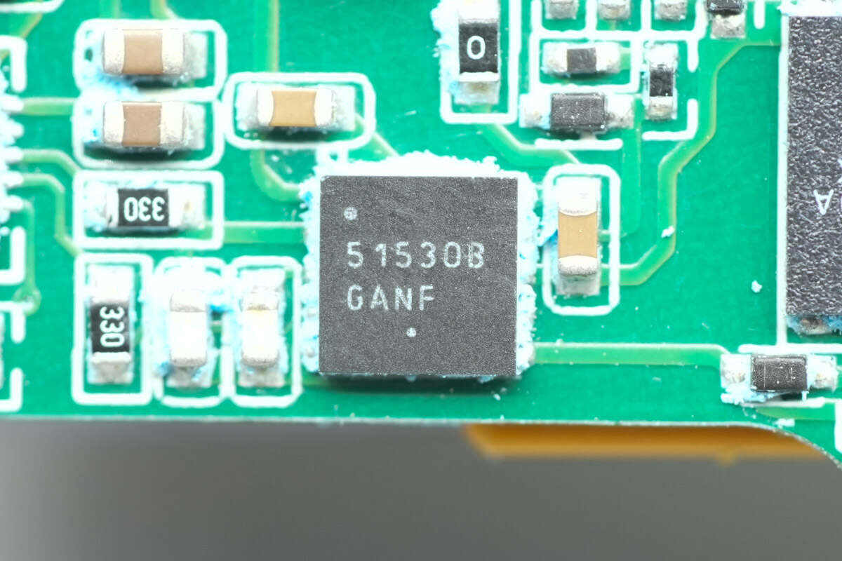
The driver for the two GaN FETs is from Onsemi, model NCP51530B. It is a 700 V high- and low-side driver with 3.5 A/3 A driving capability, suitable for AC/DC power supplies and inverters. It offers optimal propagation delay, low quiescent current, and low switching current during high-frequency operation.
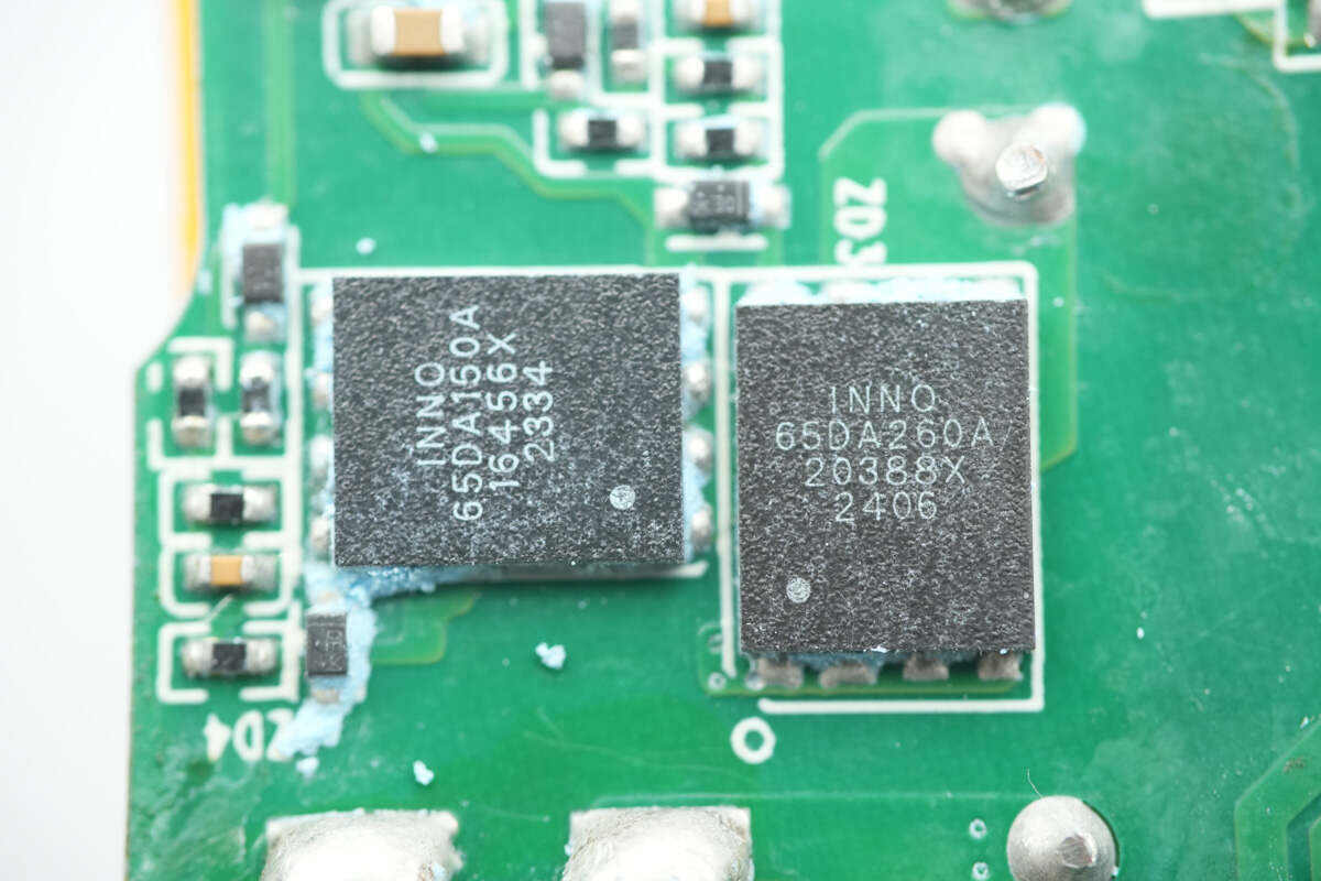
The MOSFETs are from Innoscience, model INN650DA260A. They are high-performance, cost-effective GaN high-voltage devices rated at 650 V, with a transient voltage tolerance of 750 V. Thanks to process improvements, their performance is significantly enhanced, making them suitable for 65–120 W flyback designs and 120–200 W LLC topologies.
They support ultra-high switching frequencies, have zero reverse-recovery charge, very low gate and output charges, and meet JEDEC standards for industrial applications. They also feature built-in ESD protection and comply with RoHS, lead-free, and EU REACH regulations.
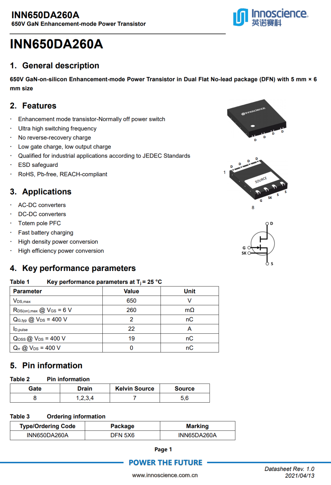
Here is the information about Innoscience INN650DA260A.
Close-up of a transformer.
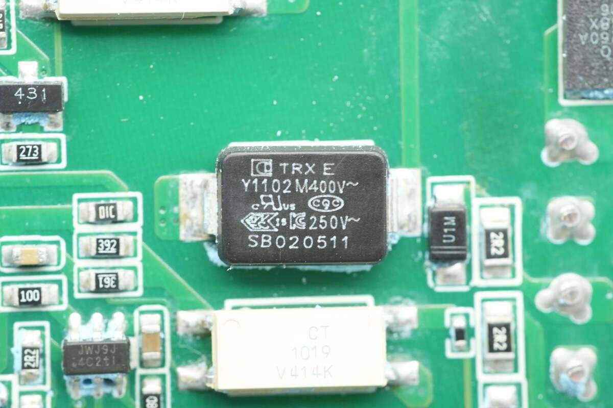
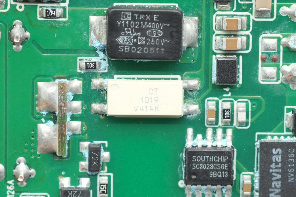
Another SMD Y capacitor is used, with part number TMY1102M.
The CT 1019 optocoupler is used for output voltage feedback.
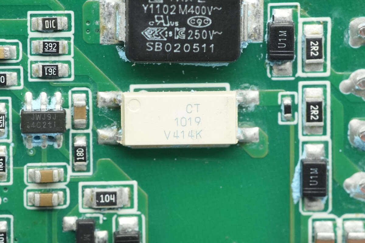
Close-up of another CT 1019 optocoupler.
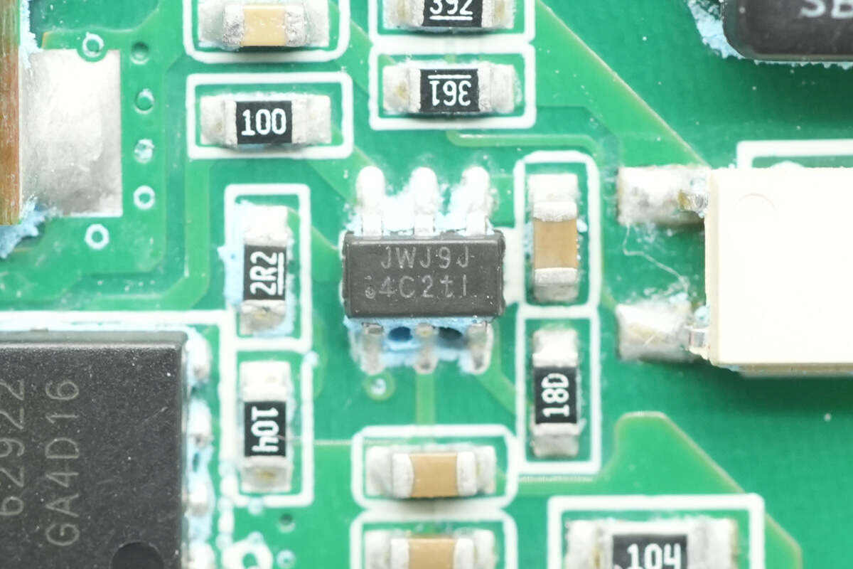
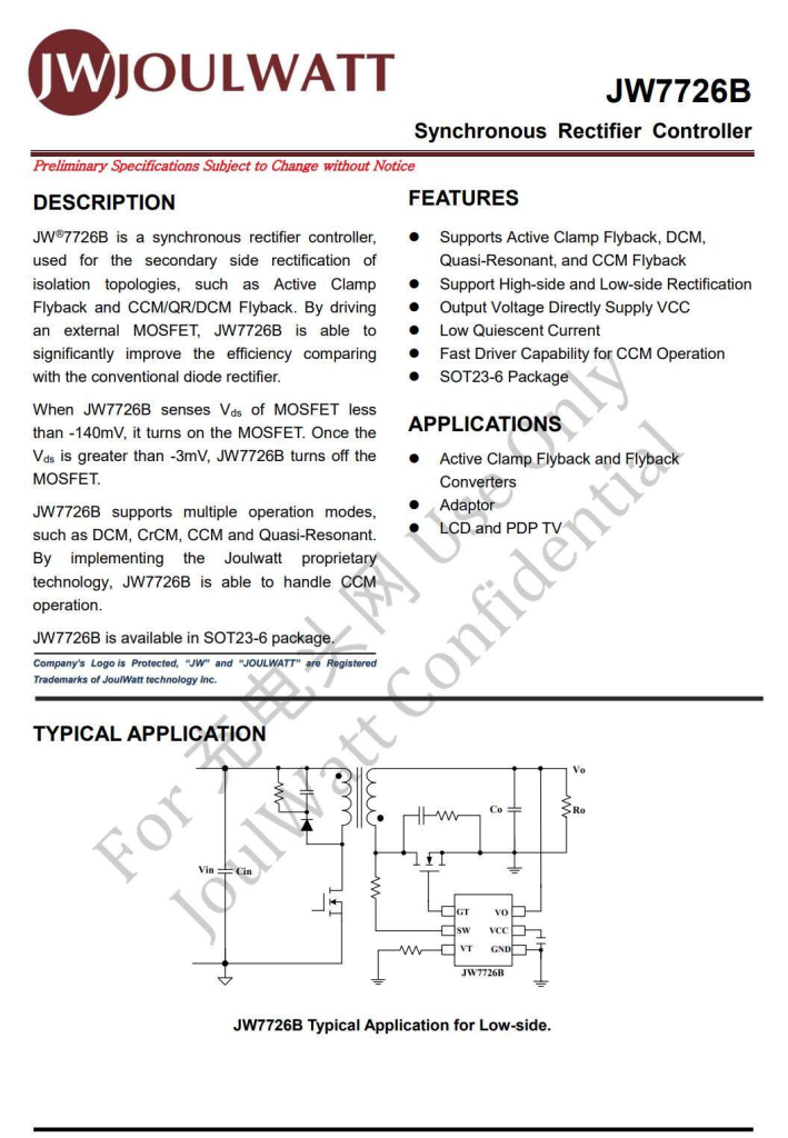
The synchronous rectifier controller is from JOULWATT, marked JWJ9J, model JW7726B. It supports CCM, DCM, QR, and ACF modes, effectively preventing false turn-on of the synchronous rectifier MOSFET during ringing. It features fast turn-off capability to remain compatible with CCM and prevents the gate from being coupled to the turn-on voltage during startup (before VCC is established). The controller supports both high-side and low-side synchronous rectification, offering flexible applications.
The JOULWATT JW7726B features low quiescent current and an output voltage detection function for automatic power source switching. When the output voltage exceeds 4.6 V, it is powered from the output voltage to reduce losses on the regulator. When the output voltage drops below 4.5 V, it is powered from the switching pin. The device comes in a SOT23-6 package with minimal external components required.
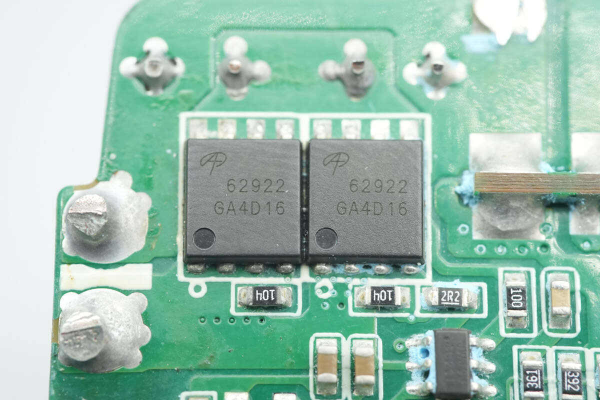
The synchronous rectifiers are from AOS, model AONS62922. They are 120 V NMOS devices with an on-resistance of 5.8 mΩ, packaged in a 5×6 mm DFN.
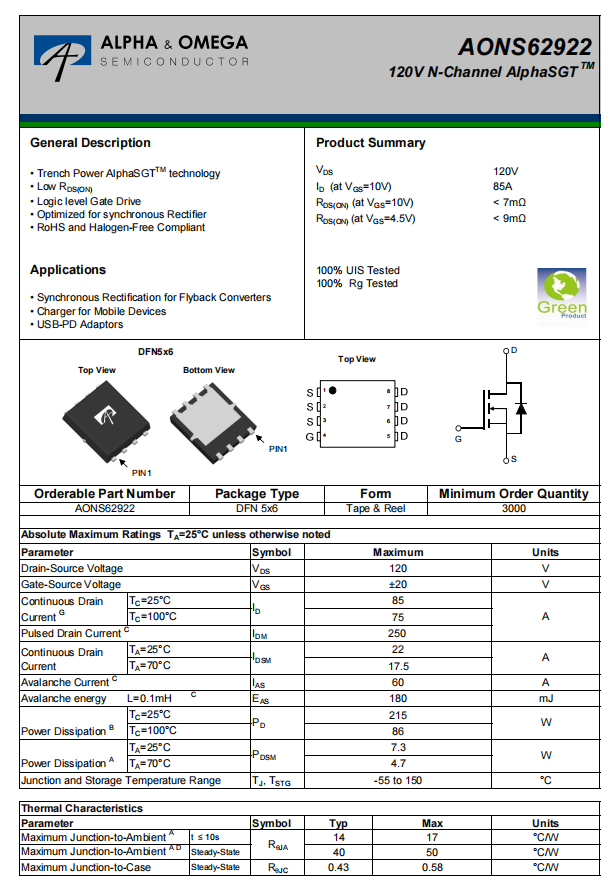
Here is the information about AOS AONS62922.
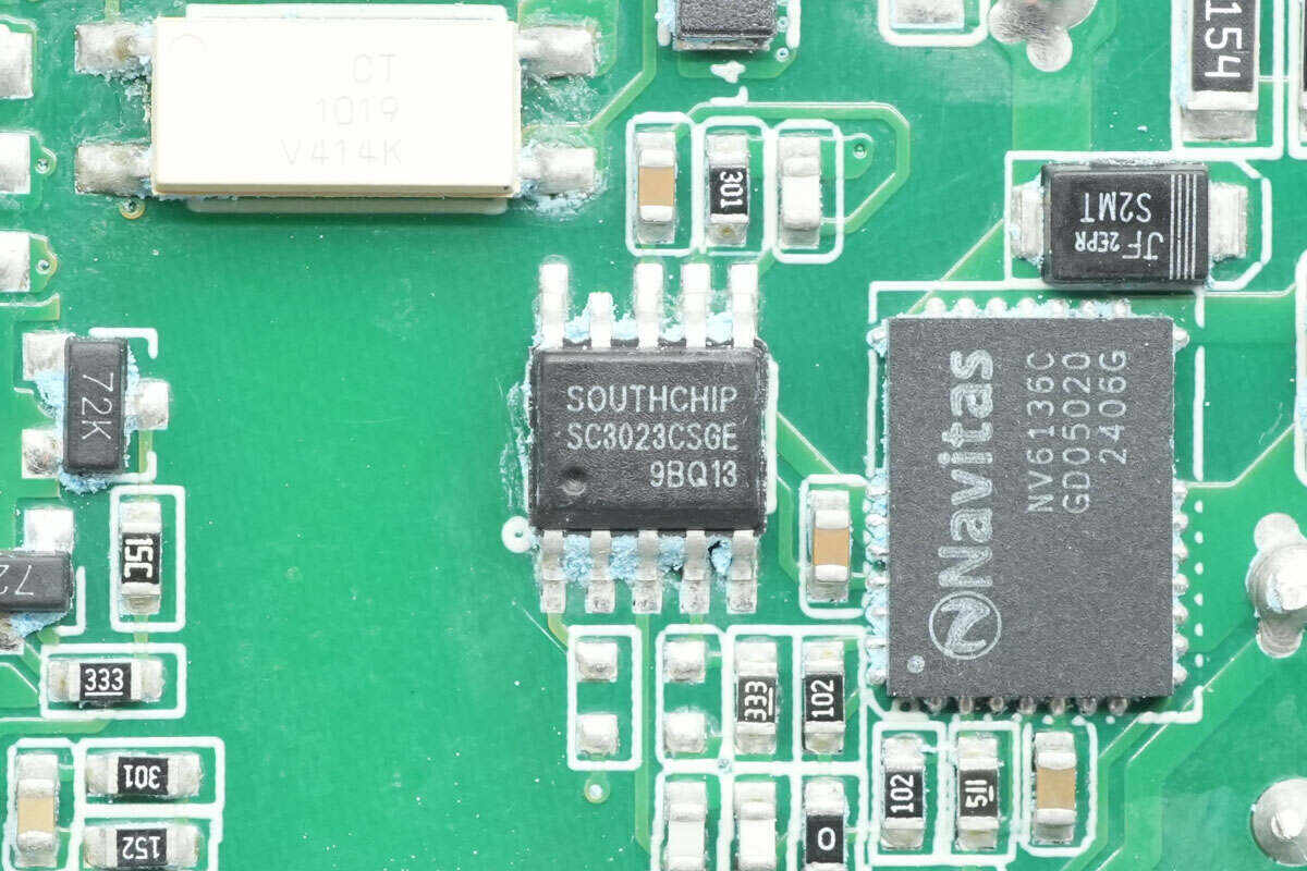
The master control chip is from SouthChip, model SC3023. It is a high-frequency quasi-resonant flyback controller with a built-in GaN driver, capable of directly driving GaN FETs. It features X-capacitor discharge, high-voltage startup, and adaptive switching frequency valley-skipping for higher efficiency across the full load range. In QR and DCM modes, it achieves high efficiency through valley turn-on. During no-load operation, it enters a low-power mode to reduce standby consumption. The chip also integrates comprehensive protection functions, supporting both internal and external over-temperature protection.
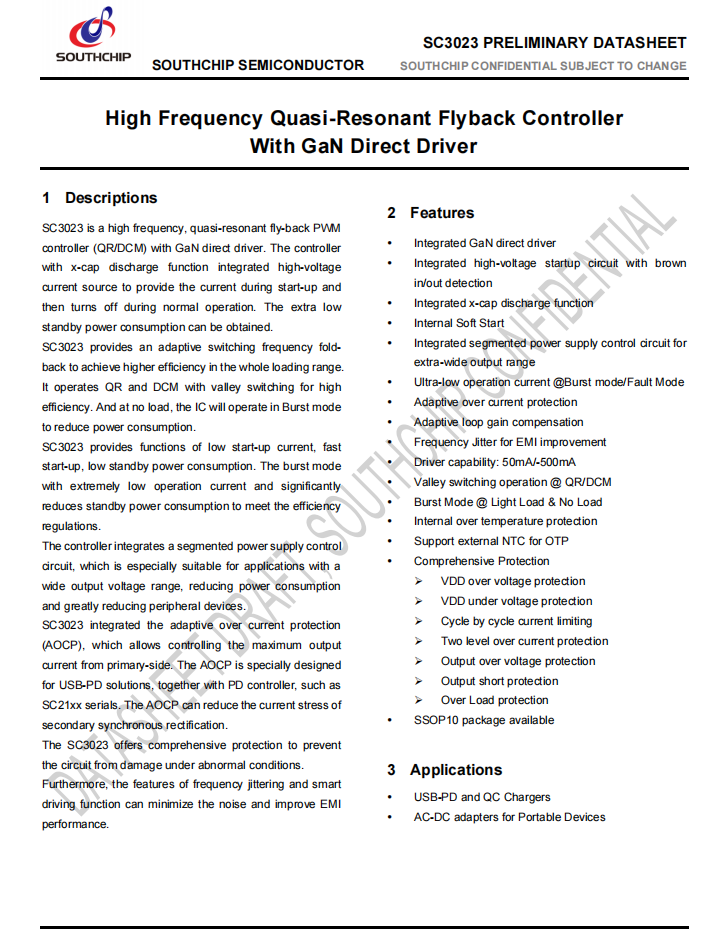
Here is the information about SouthChip SC3023.
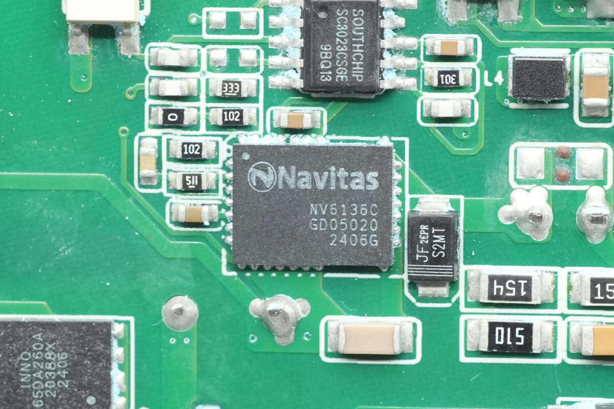
The flyback MOSFET uses the Navitas NV6136C GaN power device.
The flyback transformer is tightly wrapped with tape for insulation.
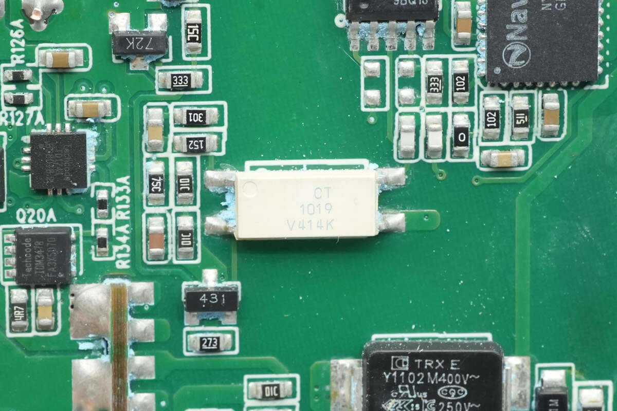
Close-up of the CT 1019 optocoupler.
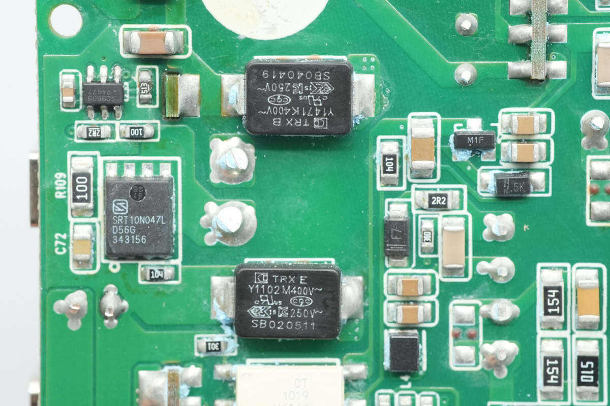
Two TRX Y capacitors are used, with part numbers TMY1471K and TMY1102M.
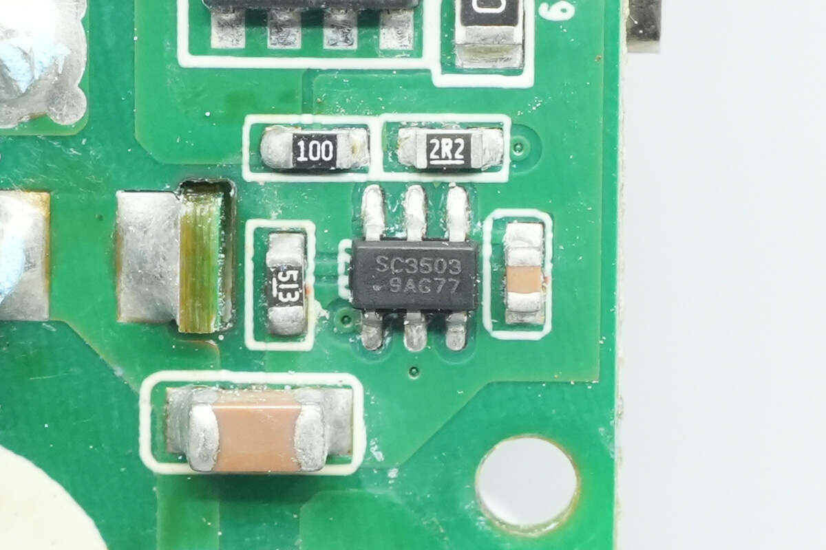
The synchronous rectifier controller is from SouthChip, model SC3503. It features adaptive turn-on detection and fast turn-off for synchronous rectification, requiring no auxiliary winding for power. It can operate with output voltages as low as 0 V. Its patented adaptive turn-on detection circuit prevents false conduction of the synchronous rectifier, is compatible with various MOSFETs, and has ultra-low quiescent current. It supports multiple operating modes, high-side and low-side synchronous rectification, and requires very few external components.
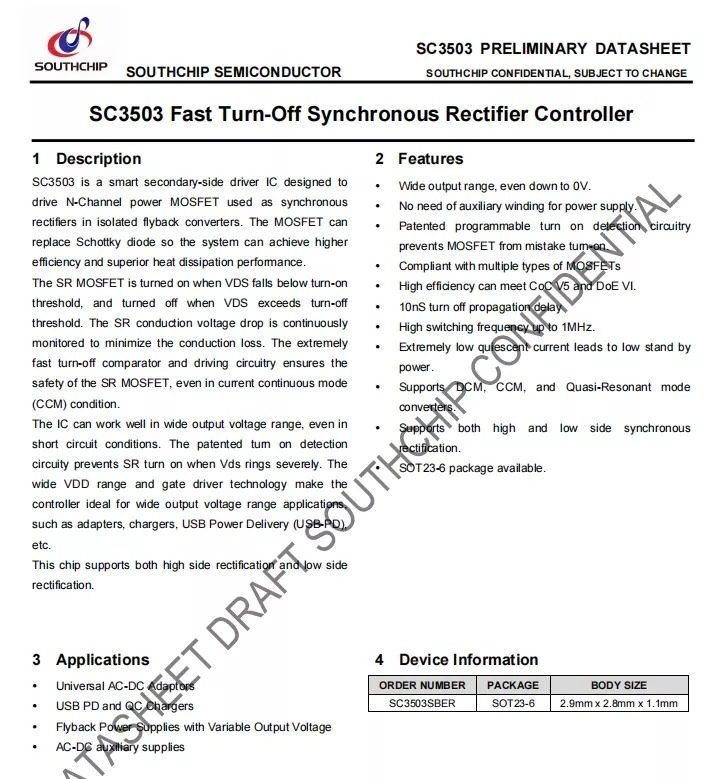
Here is the information about SouthChip SC3503.
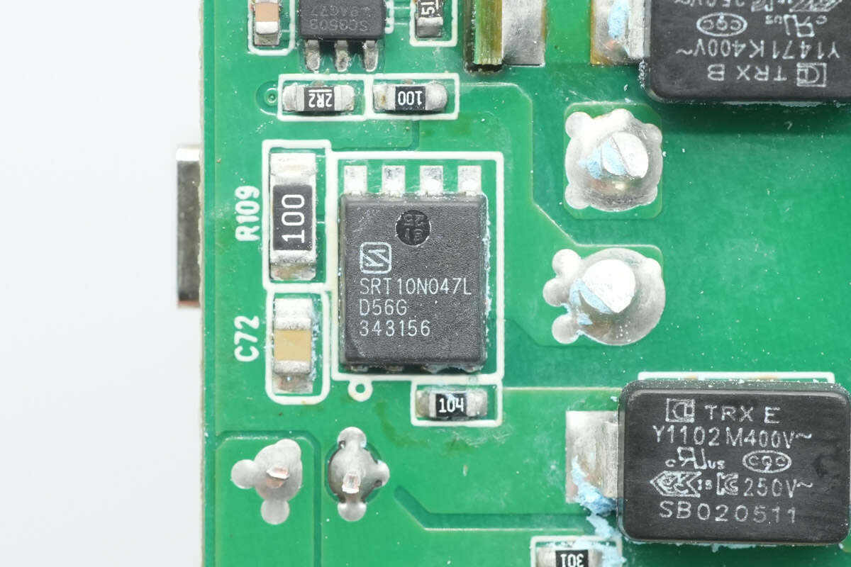
The synchronous rectifier is from Sanrise, model SRT10N047L. It is a 100 V NMOS with an on-resistance of 3.9 mΩ, packaged in a 5×6 mm PDFN.
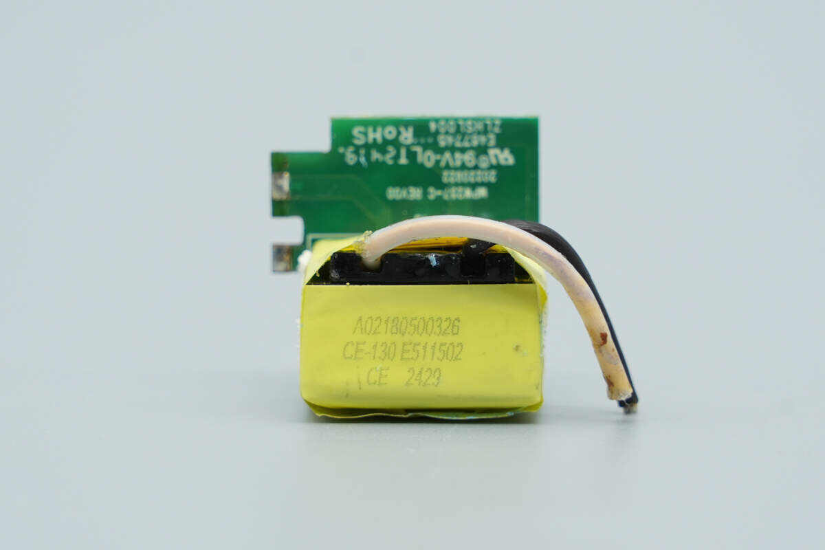
Another small PCB hosts a switching transformer.
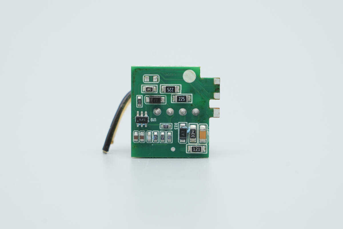
The back side of the PCB is soldered with the switching power supply controller.
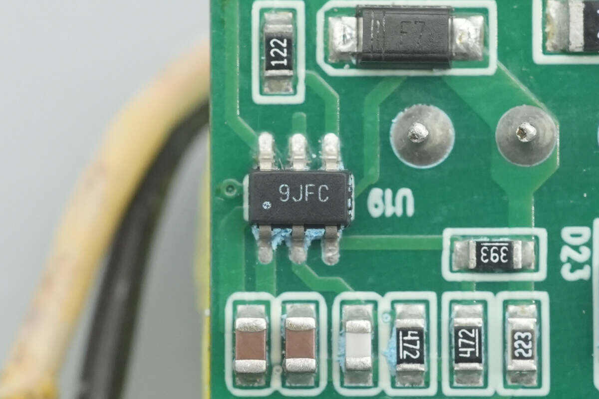
The controller is marked with 9JFC.
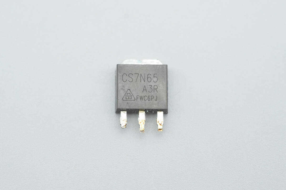
The primary MOSFET is from CR MICRO, model CS7N65A3R. It is a 650 V NMOS with an on-resistance of 1.2 Ω, packaged in TO-251.
Close-up of the transformer.
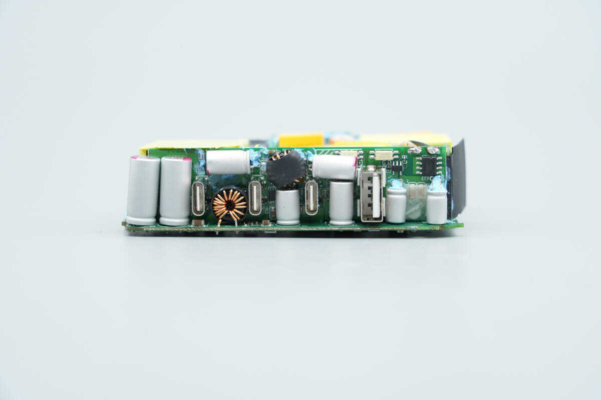
The output side features four solid capacitors along with the output PCB.
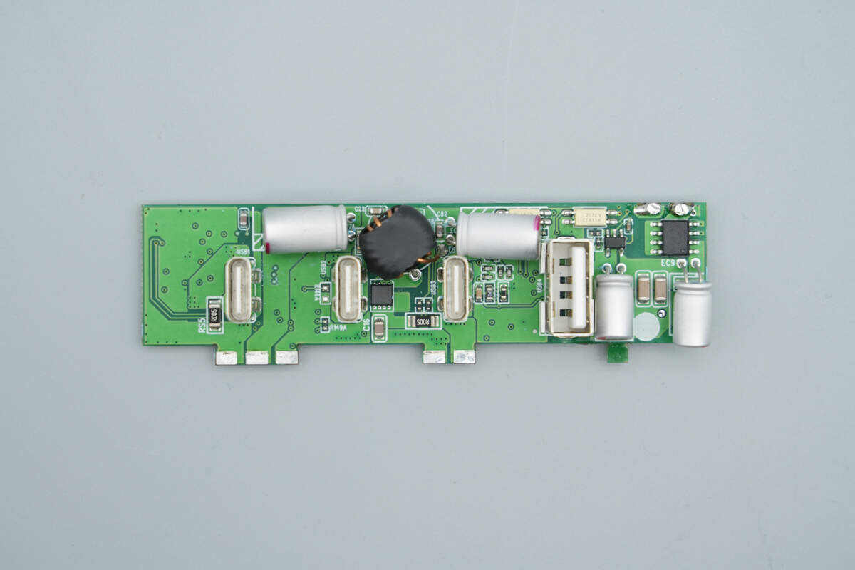
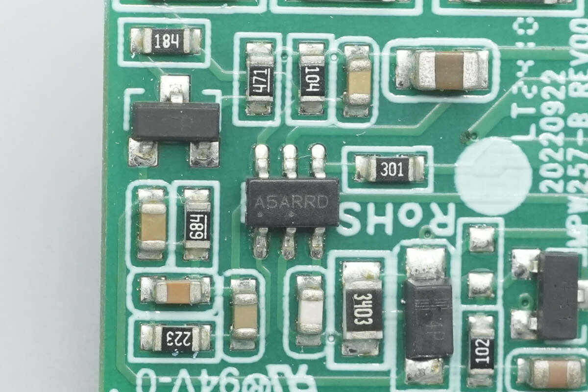
Remove the output PCB. The front side reveals filter solid capacitors, the synchronous rectifier controller, and sockets.
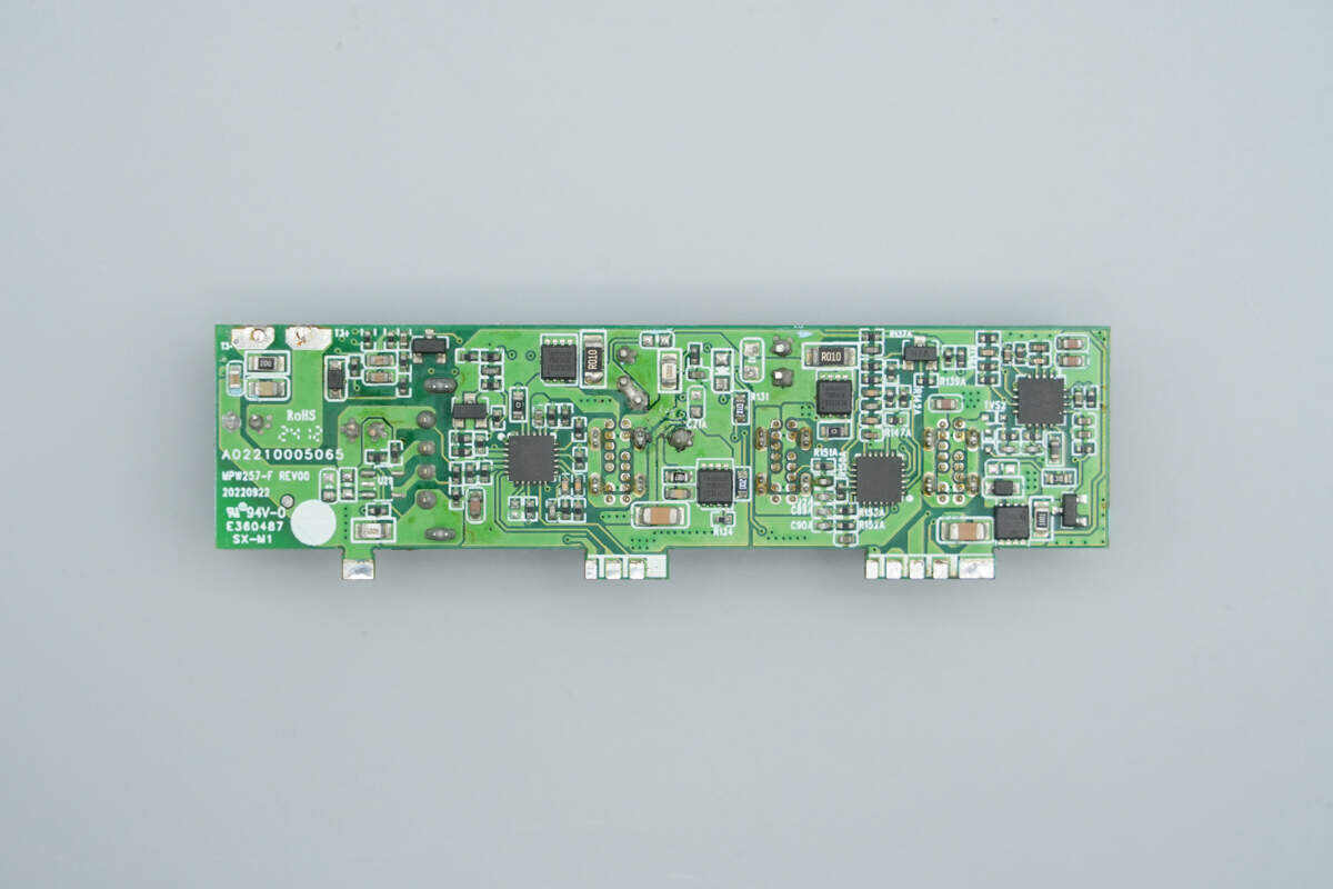
On the back side, in addition to the protocol chips and VBUS MOSFETs corresponding to the three USB-C ports, there is also a synchronous buck MOSFET.
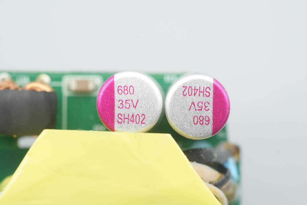
These two solid capacitors are both rated at 35 V, 680 μF.
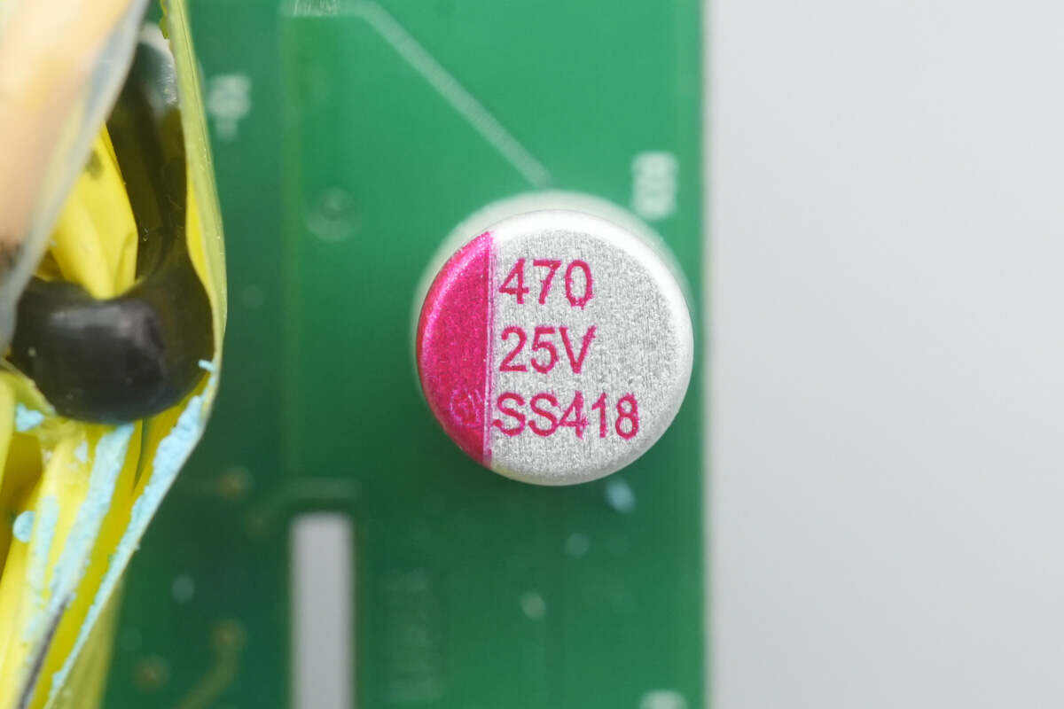
The third solid capacitor is rated at 25 V, 470 μF.
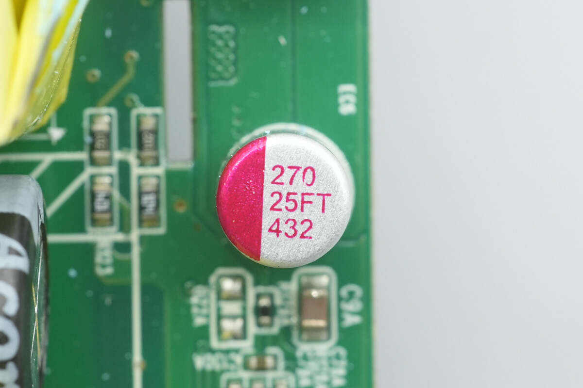
The fourth solid capacitor is rated at 25 V, 270 μF.
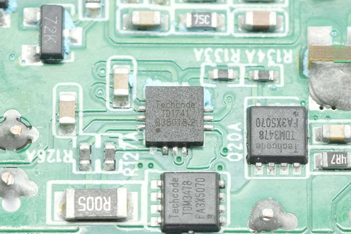
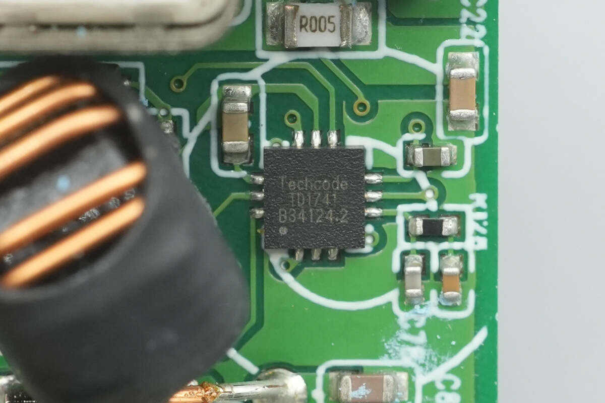
The synchronous buck controller is from Techcode, model TD1741. It supports a 40 V input and 28 V output, provides precise constant voltage/constant current control, and supports burst and PFM modes to improve light-load efficiency. The chip features dual independent output current sensing and offers comprehensive protection functions.
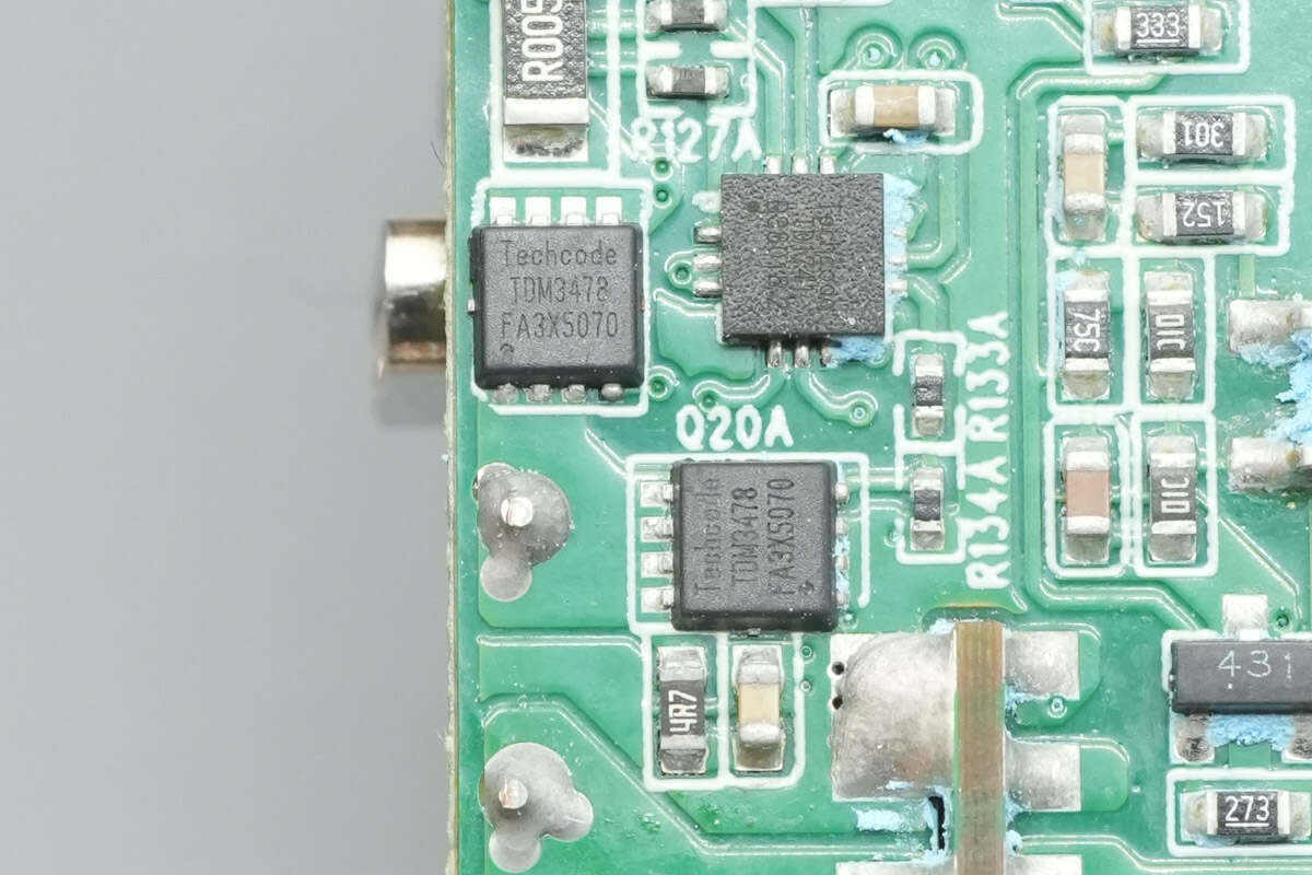
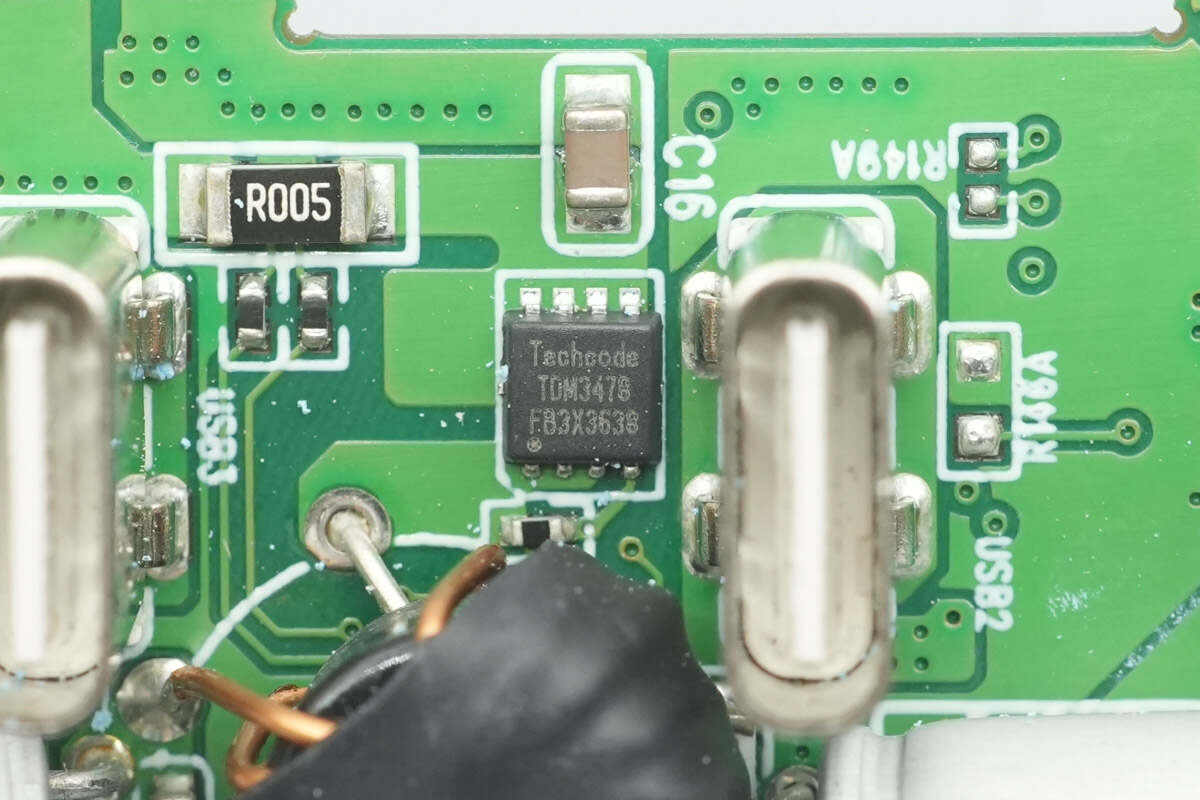
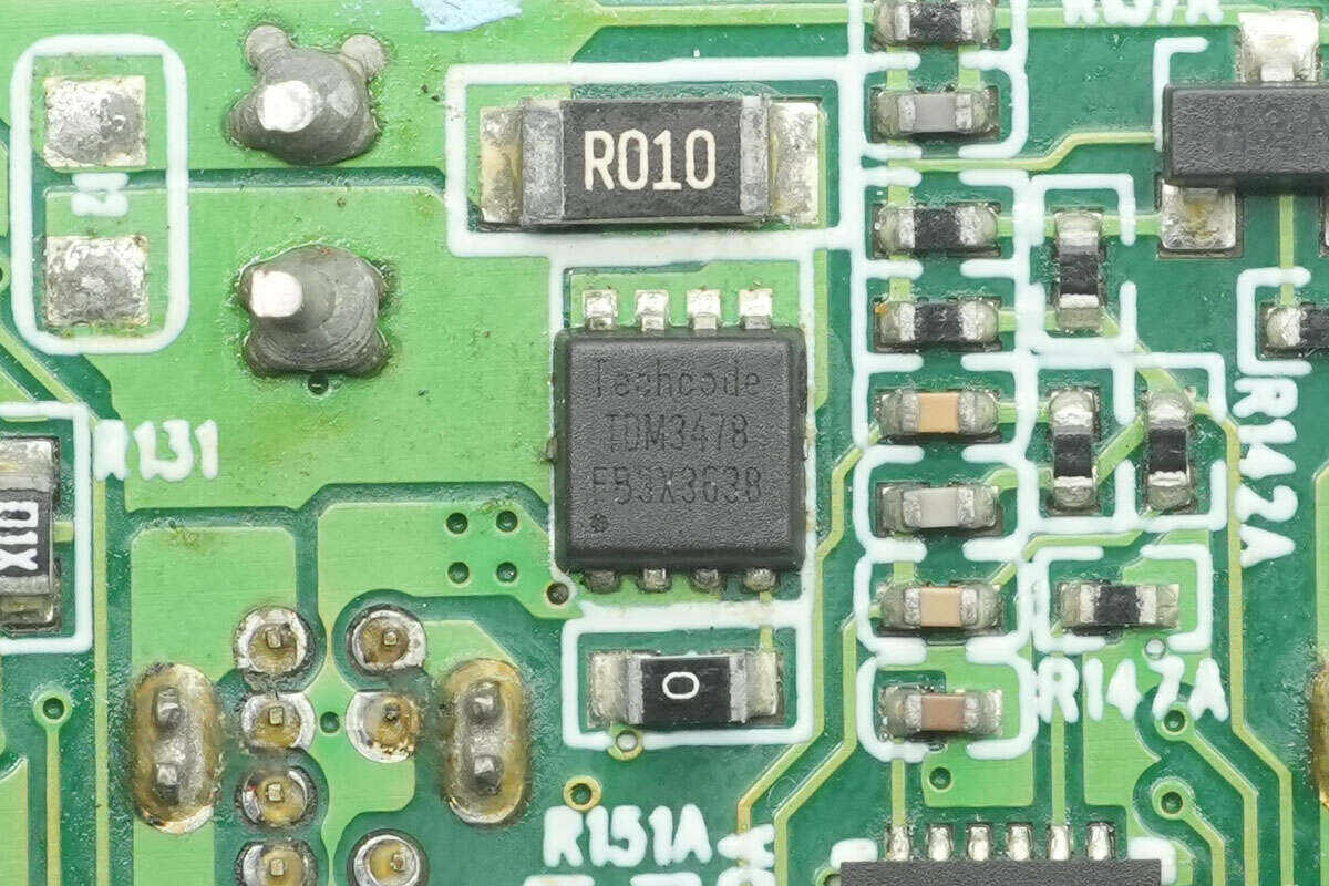
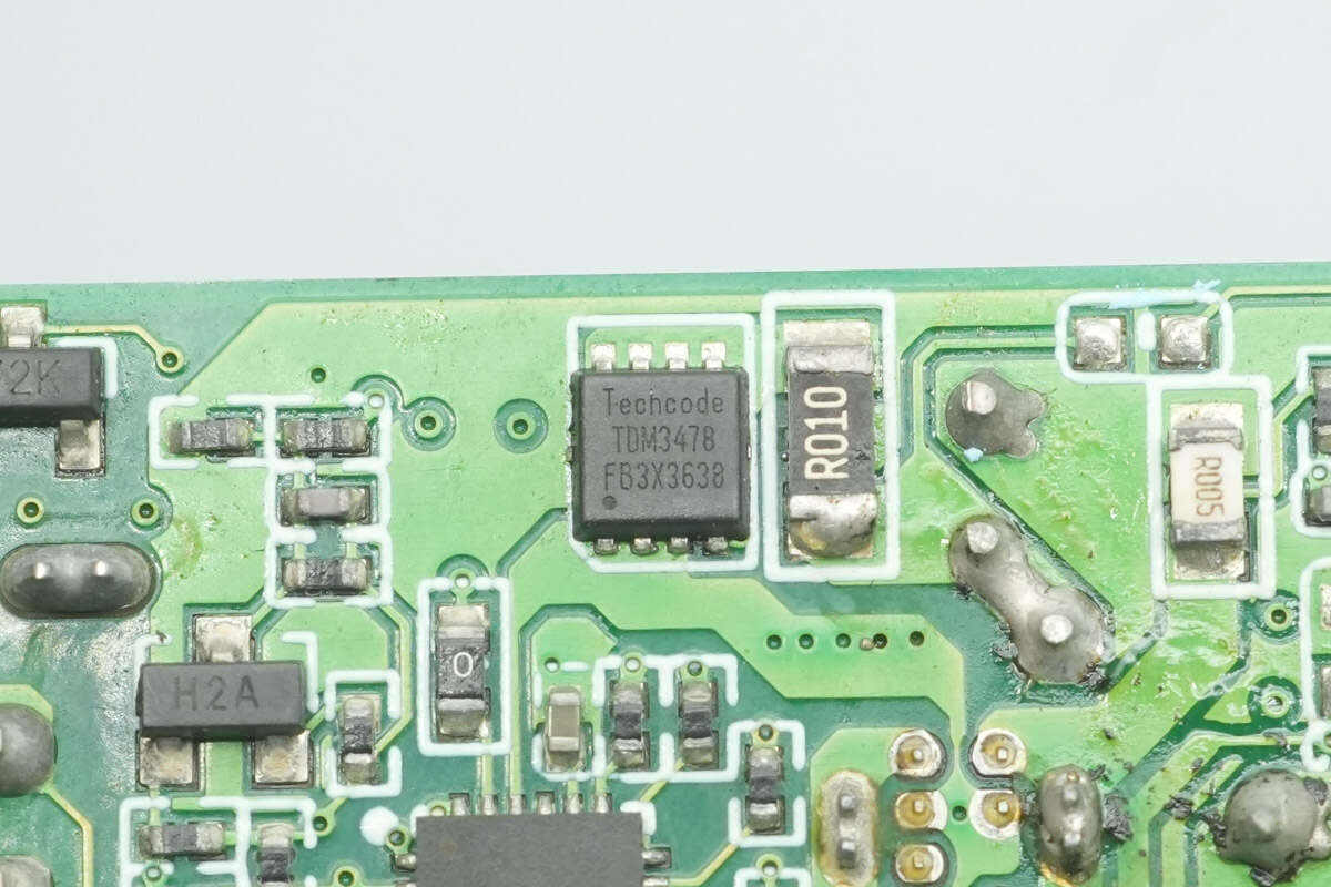
The synchronous buck MOSFETs are also from Techcode, model TDM3478. They are 30 V NMOS devices with an on-resistance of 5 mΩ, packaged in PPAK-3×3-8.
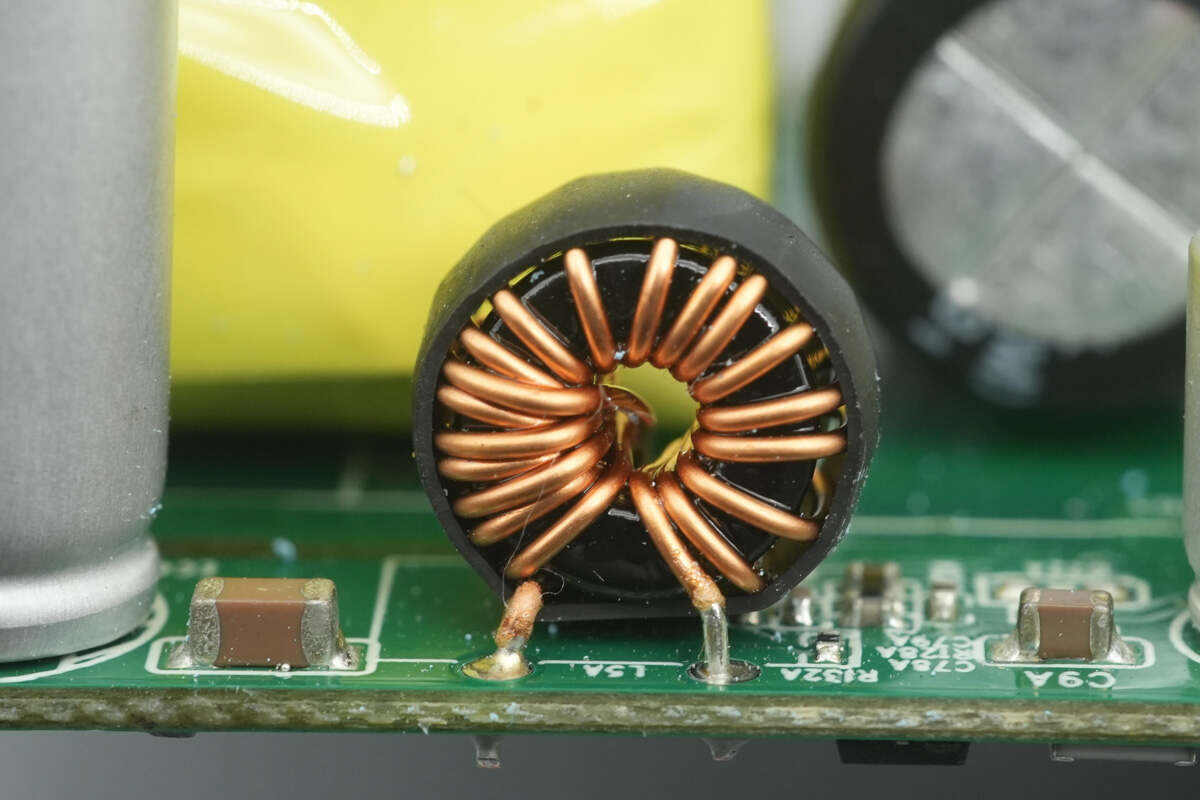
The buck inductor is insulated with a heat-shrink tube.

The protocol chip for the USB-C1 port is from Weltrend, model WT6676F. It supports USB PD 3.1 with up to 36 V output, programmable constant voltage/constant current control, an internal low-side current-sense amplifier, and line-loss compensation.
The WT6676F also features programmable protection functions, including over-voltage, under-voltage, over-current, and over-temperature protection. It has a built-in 10-bit ADC for voltage and current monitoring, an NMOS load switch driver, an output discharge MOSFET, integrated voltage regulation, PFC control support, and an energy-saving mode. The input voltage can reach up to 45 V, and it comes in a QFN-16 package. A thermistor is soldered next to the chip to monitor the internal temperature of the charger for over-temperature protection.
The VBUS MOSFET for the USB-C1 port is from Techcode, model TDM3482. It is a 40 V NMOS with an on-resistance of 7.9 mΩ, packaged in PPAK-3×3-8.
The synchronous buck controller for the other buck channel also uses the Techcode TD1741.
The synchronous buck MOSFETs also use the Techcode TDM3478.
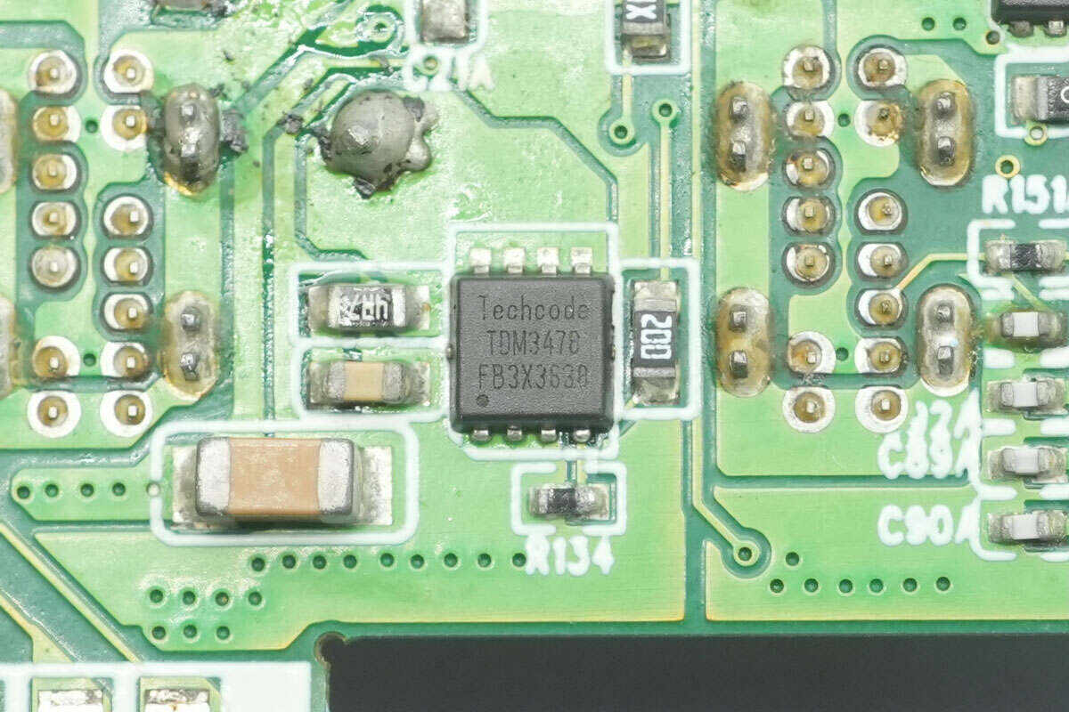
Another Techcode TDM3478 synchronous buck MOSFET is located on the back side of the PCB.
Close-up of the buck inductor.
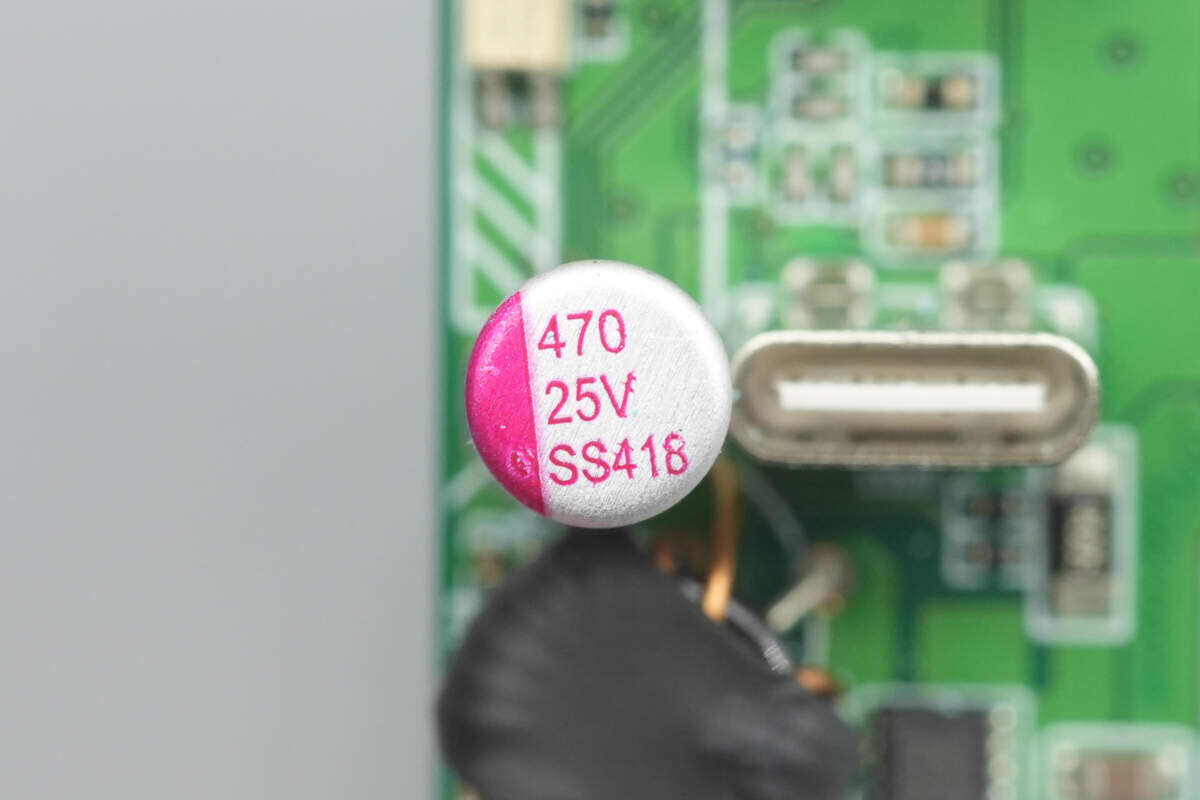
The solid capacitor is rated at 25 V, 470 μF.
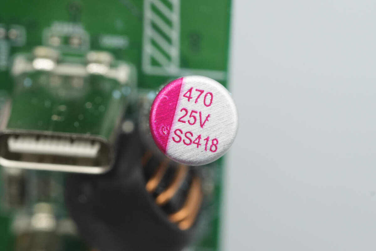
Another capacitor with the same model is also used.
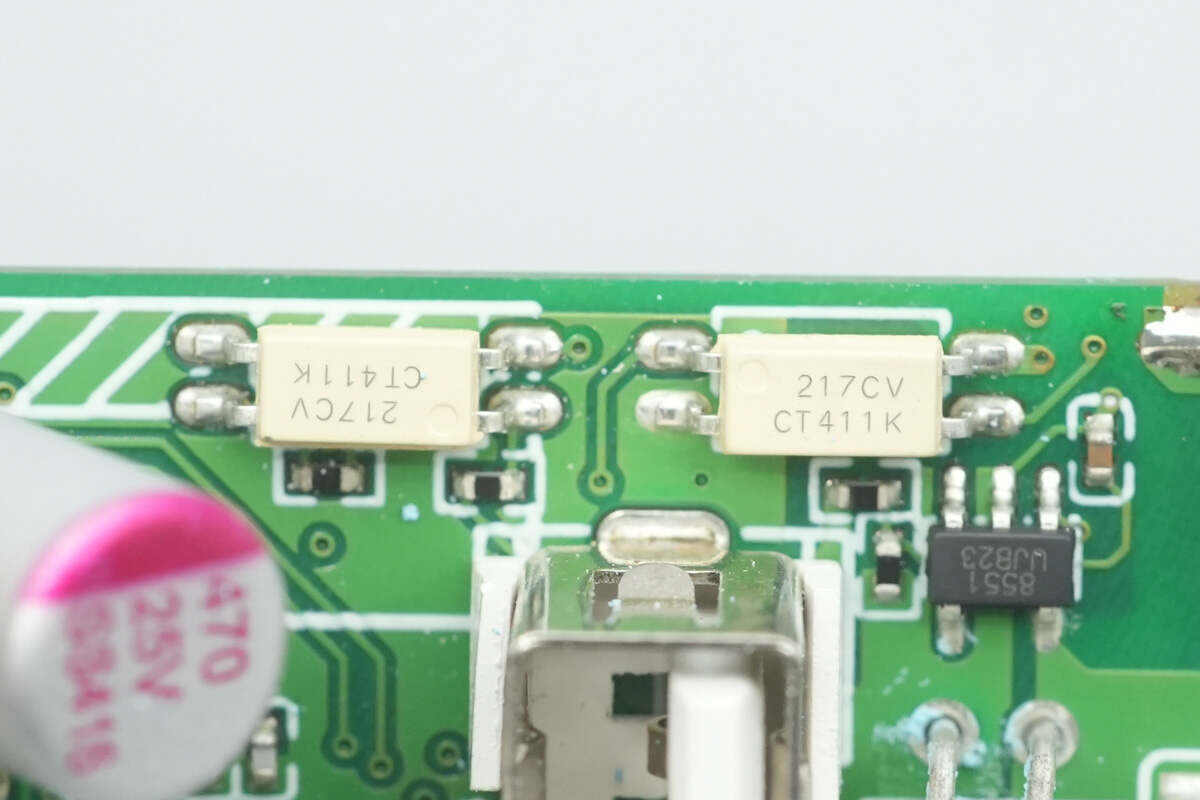
Two optocouplers are used for output power switching control.
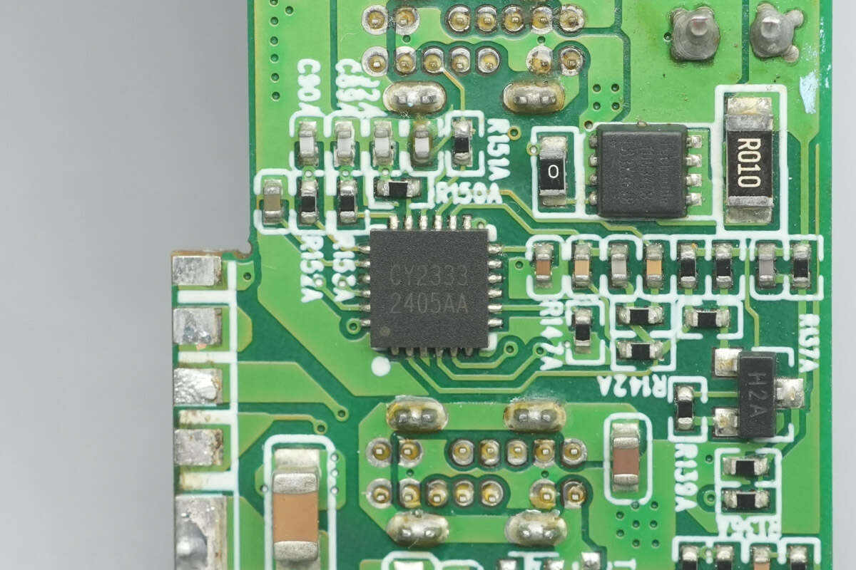
The protocol chip for the USB-C2 port is from Canyon, model CY2333. It is compatible with USB Type-C Specification Rev 1.2, USB PD Rev 3.0 V1.1, and QC5.
The VBUS MOSFET for the USB-C2 port uses the Techcode TDM3478.
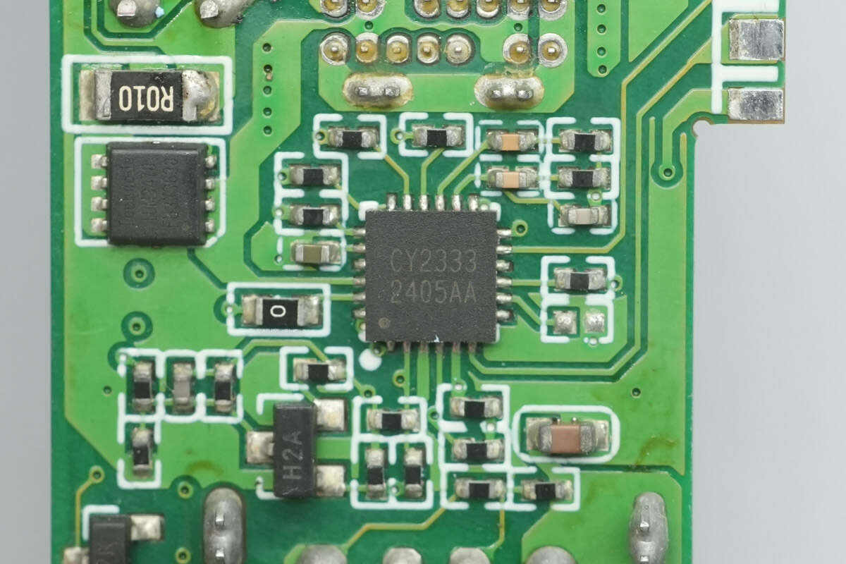
The USB-C3 port also uses the Canyon CY2333 protocol chip.
The VBUS MOSFET for the USB-C3 port is also the Techcode TDM3478.
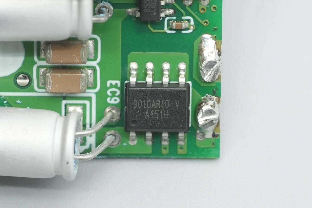
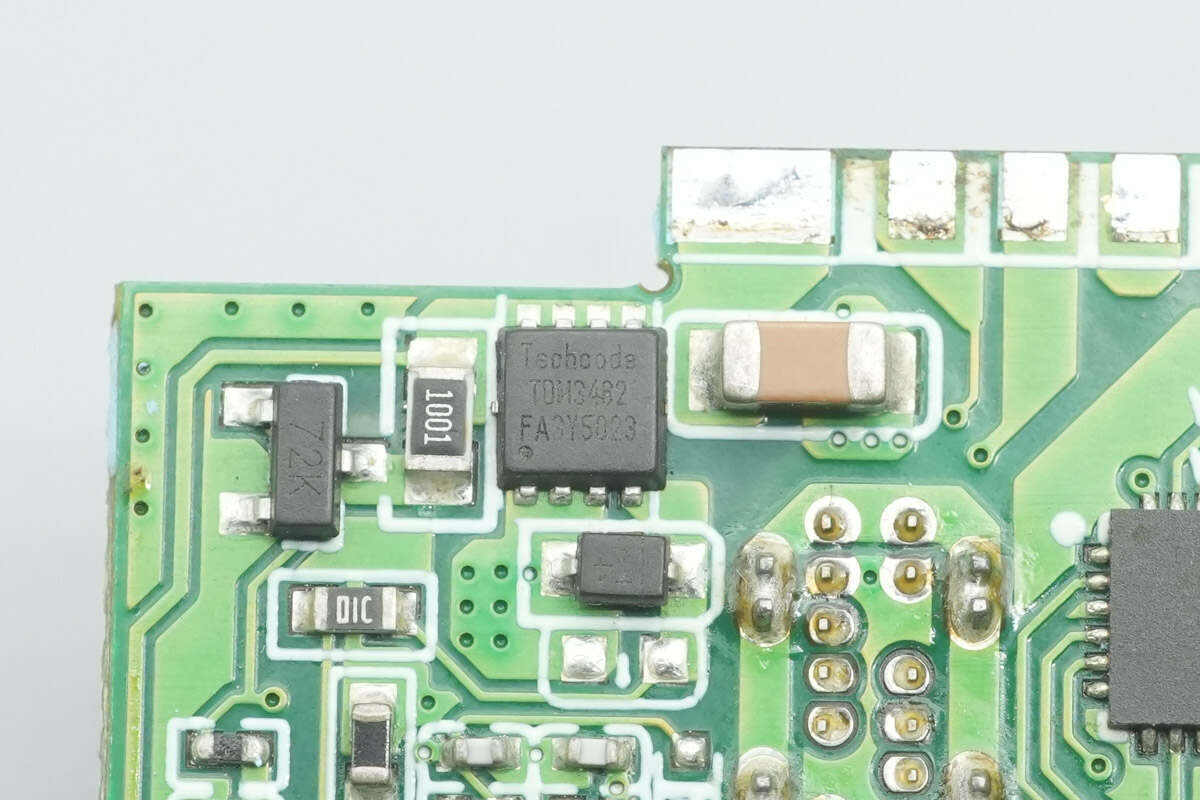
The synchronous rectifier controller for the USB-A port is from HYASiC, model HYC9010.
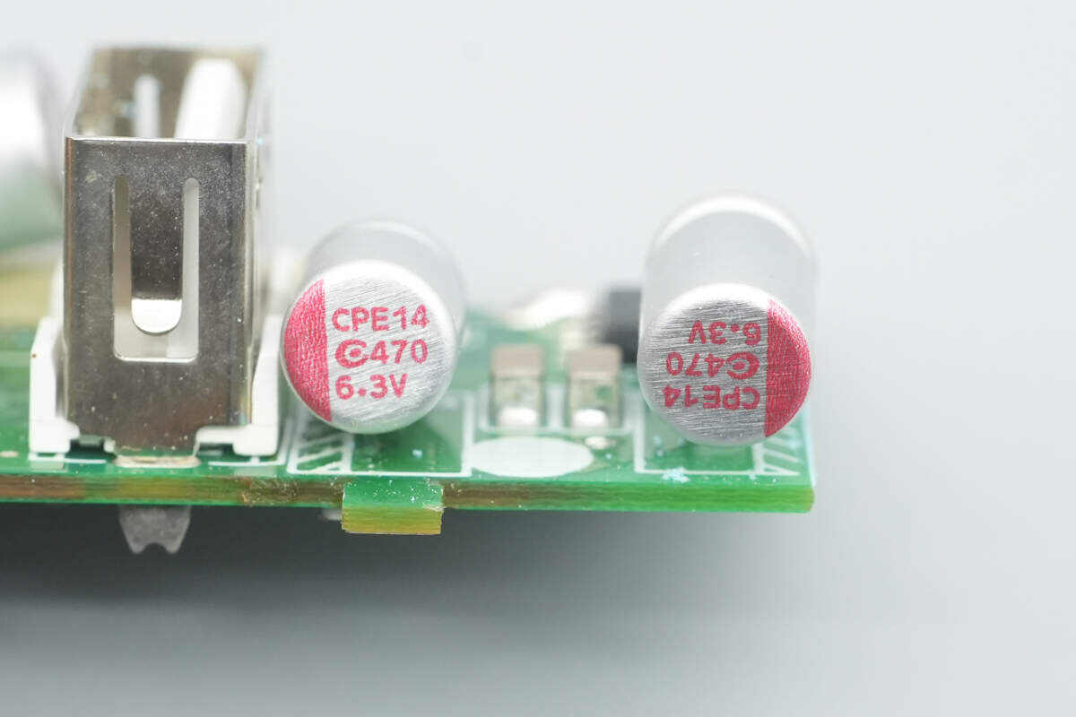
The two output filter capacitors are from APAQ, each rated at 6.3 V, 470 μF.
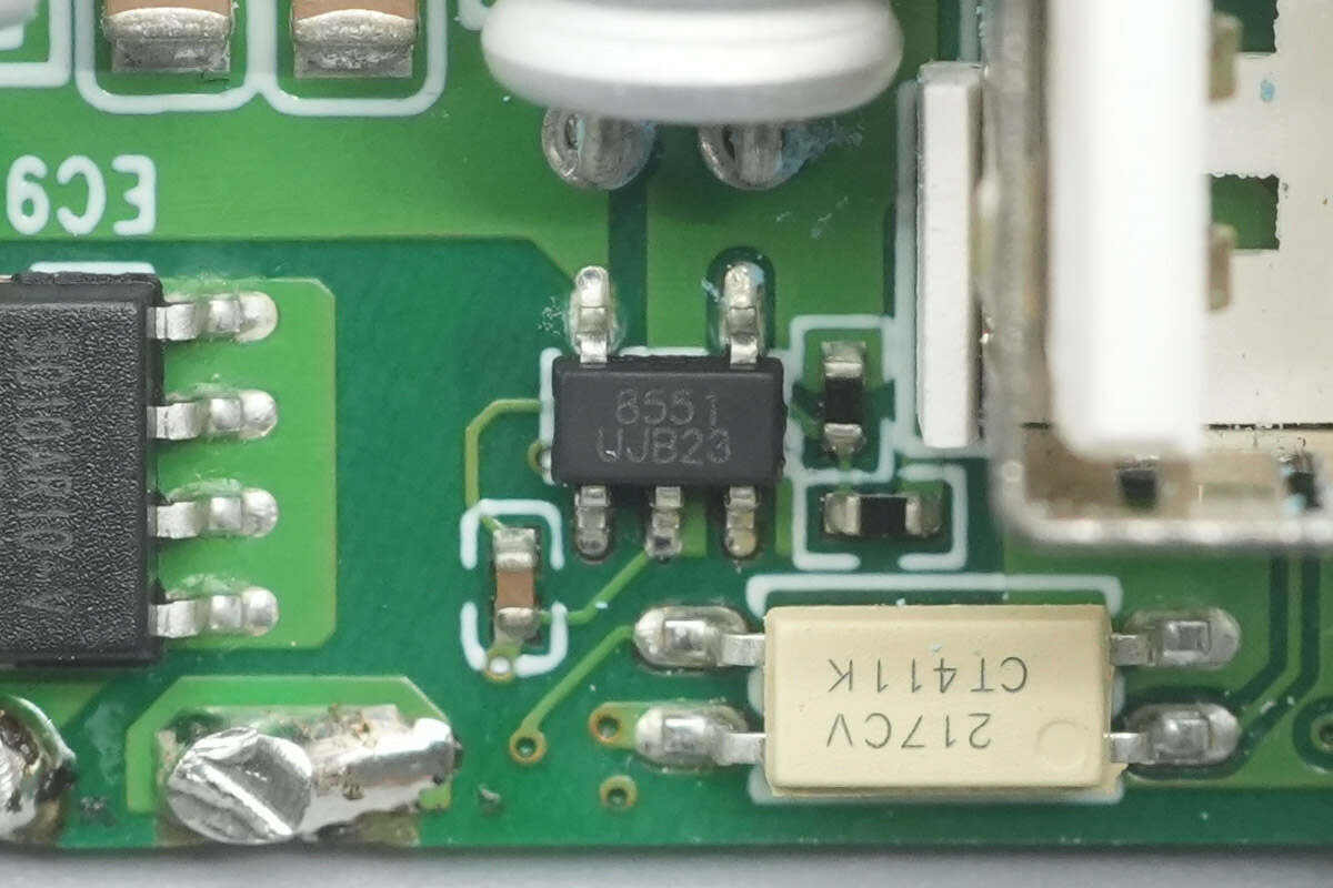
An auto-identification chip marked 8551 is used for the USB-A port protocol functions.
Well, those are all components of the Belkin BoostCharge Pro 140W 4-Port GaN Wall Charger.
Summary of ChargerLAB
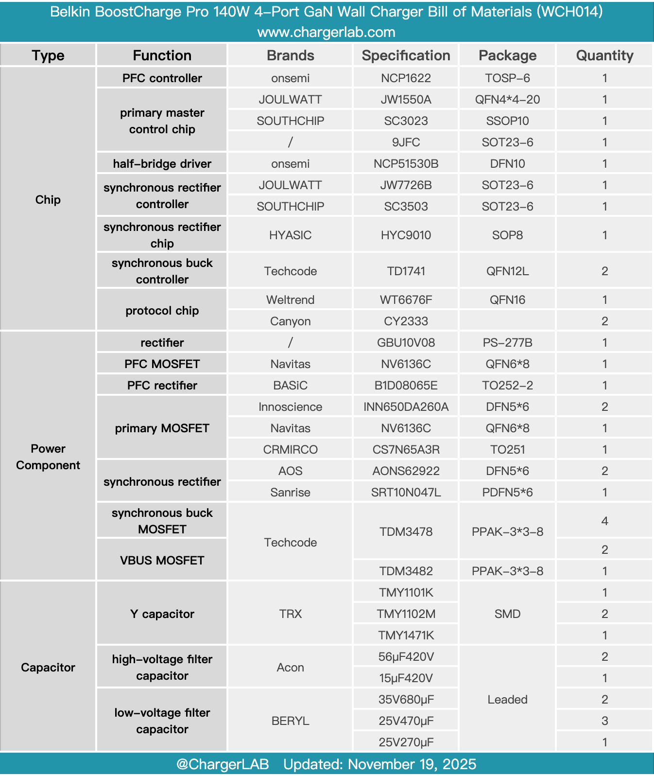
Here is the component list of the Belkin BoostCharge Pro 140W 4-Port GaN Wall Charger for your convenience.
The casing is made of recycled plastic. The plug features a detachable modular design, enabling easy replacement for use in various countries and regions. It supports up to 140 W PD 3.1, as well as 65 W + 65 W and 65 W + 45 W + 20 W fast-charging configurations.
After taking it apart, we found that it is based on a PFC boost circuit combined with a three-channel switching power supply design. The PFC stage uses the Onsemi NCP1622 paired with the Navitas NV6136C GaN power device and the BASiC B1D08065E SiC diode.
The 140 W output is managed by the JOULWATT JW1550A controller paired with the Onsemi NCP51530 driver, using Innoscience INN650DA260A GaN FETs, with voltage output controlled by the Weltrend WT6676 protocol chip. The 65 W output uses the SouthChip SC3023 GaN main controller paired with NV6136C, providing fixed-voltage output. Two buck circuits and two protocol chips regulate the output voltage.
The PCBA module is composed of multiple PCBs soldered together, improving space utilization and reducing overall size. The module uses a large metal plate for heat dissipation, with graphite thermal pads applied to enhance cooling performance.
Related Articles:
1. Teardown of SMSL GaN Power Amplifier (PA200)
2. Teardown of RedMagic 80W Air-Cooled Wireless Charging Dock (PA0404)
3. Teardown of Momax 45W 3-in-1 GaN Power Bank with Retractable Cable (IP167)