Introduction
Belkin has launched a new 100W GaN charger featuring three output ports: two USB-C ports and one USB-A port. It supports up to 100W from a single port and offers multi-port power distribution, such as 60W + 22W + 18W. The charger adopts a single-stage high-PF switched-mode power-supply architecture, which eliminates the need for a dedicated PFC controller, boost inductor, additional power components, and large high-voltage electrolytic capacitors while still achieving effective power-factor correction. This design reduces overall size and meets the requirements of high-power power-supply applications. Next, let’s take a closer look at its internal components and design.
Product Appearance
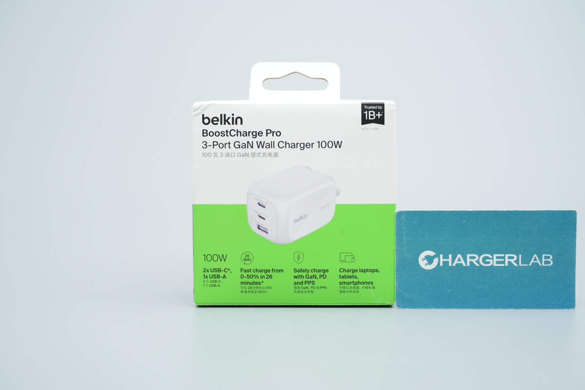
The front of the packaging displays the Belkin logo, the product name, the charger’s appearance, and its key selling points.
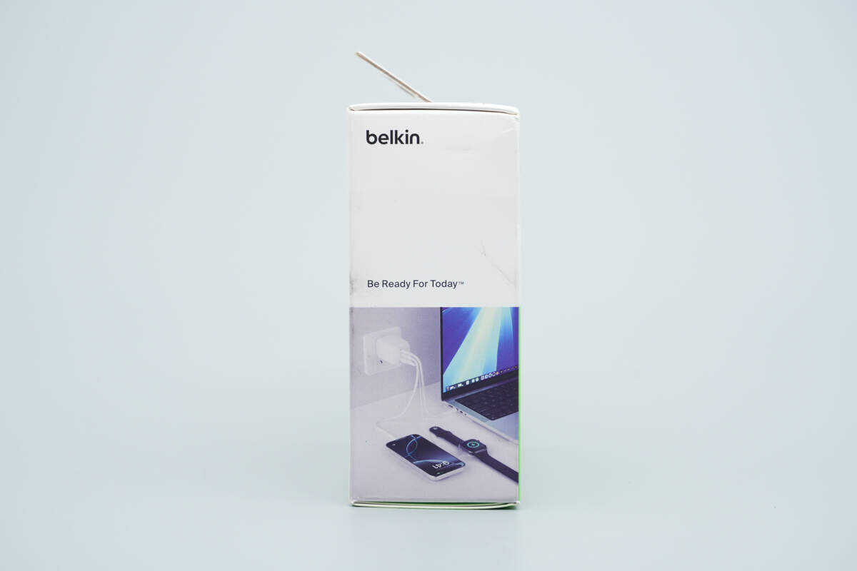
One side of the box illustrates a usage scenario showing the charger powering a laptop, a smartphone, and a smartwatch simultaneously.
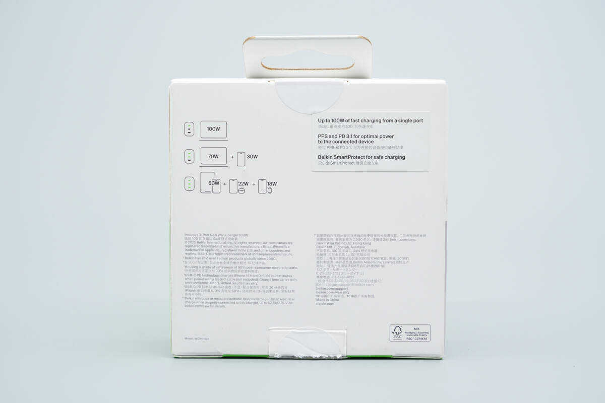
The back of the packaging shows a diagram of the port power-distribution profiles along with an overview of the charger’s key features.

The package includes the charger itself along with a user manual.
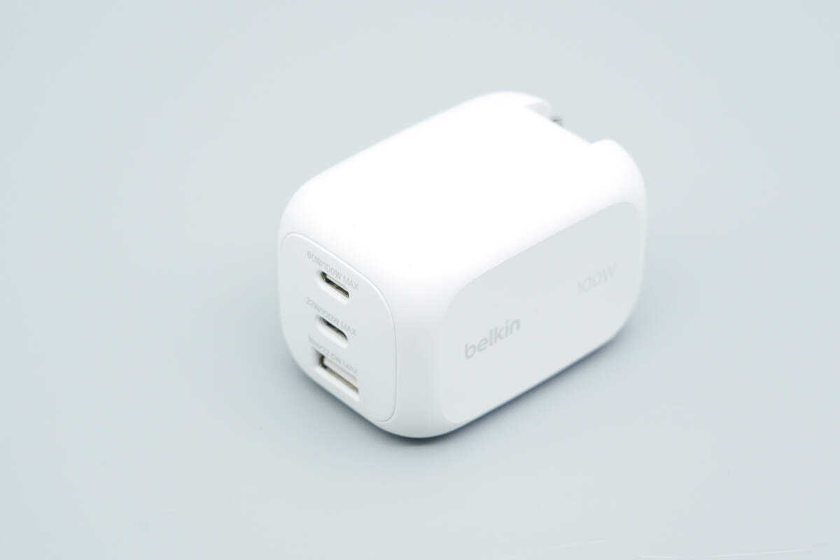
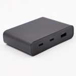
The enclosure is made of white recycled plastic with a matte finish.

One side of the charger is printed with the Belkin logo and the “100W” marking.
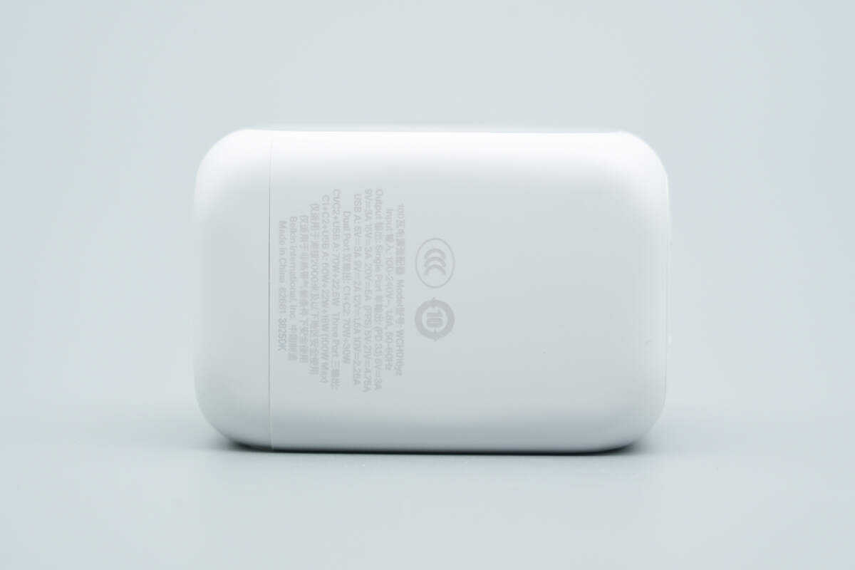
This side carries the charger’s technical specifications.
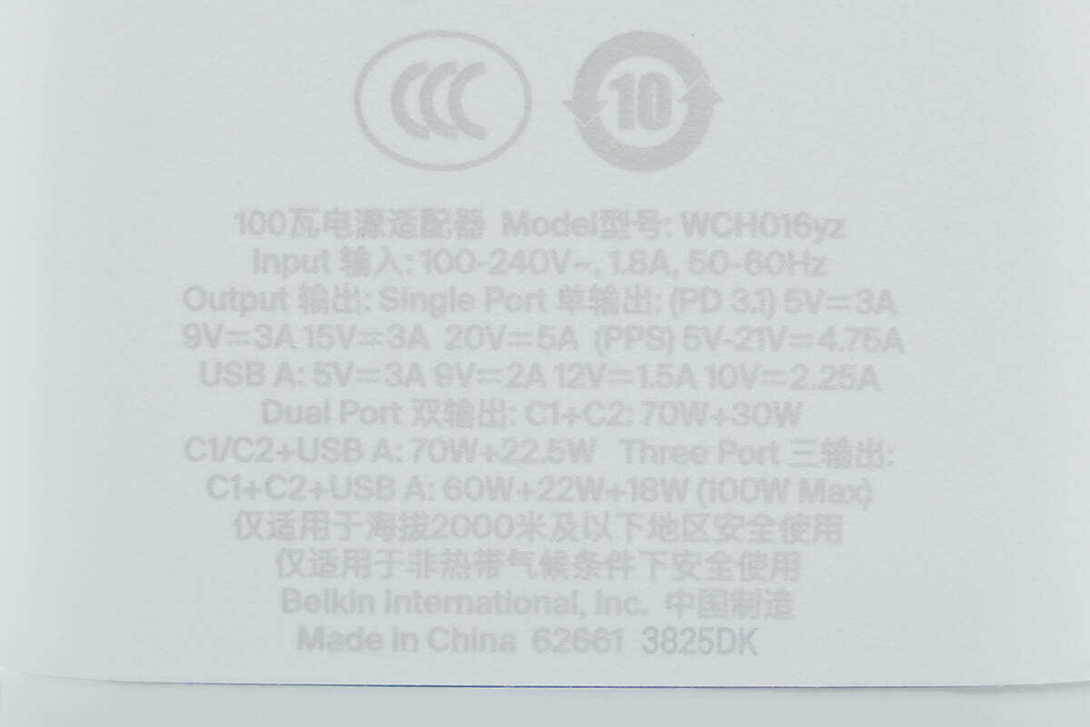
Model: WCH016yz
Input: 100–240V~ 50/60Hz 1.8A
Single-port output:
USB-C1/USB-C2: 5V 3A, 9V 3A, 15V 3A, 20V 5A
(PPS) 5–21V 4.75A
USB-A: 5V 3A, 9V 2A, 12V 1.5A, 10V 2.25A
Dual-port output:
C1 + C2: 70W + 30W
C1/C2 + USB-A: 70W + 22.5W
Three-port output:
C1 + C2 + USB-A: 60W + 22W + 18W (100W Max)
The product has passed CCC certification.

It has passed Level VI energy efficiency certification. The input-side housing features a detachable design, allowing different plug types to be swapped to meet the requirements of various countries and regions.
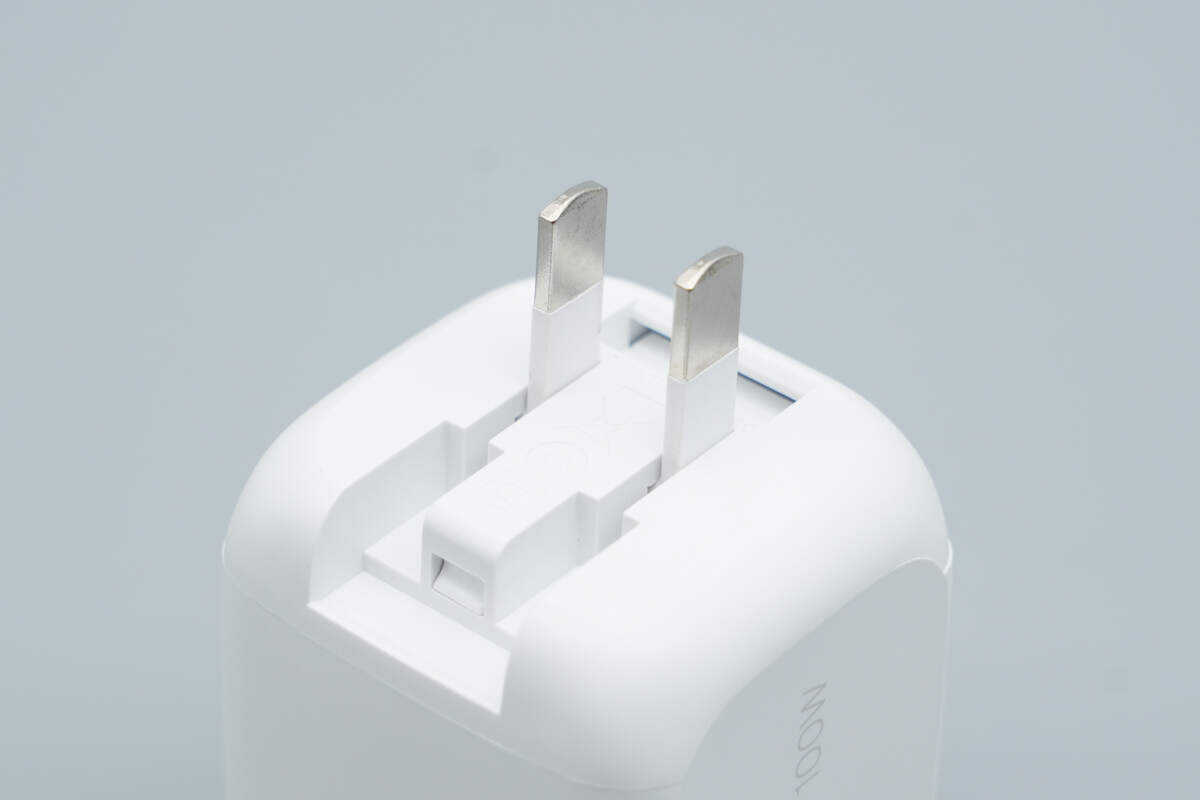
The plug is foldable.
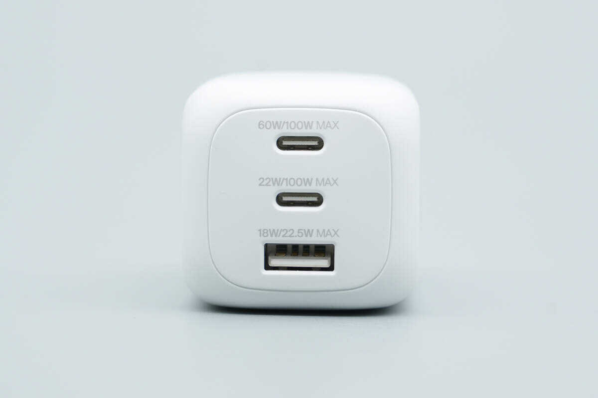
The output side is equipped with two USB-C ports and one USB-A port, with the power ratings for single- and multi-port output printed next to each port.
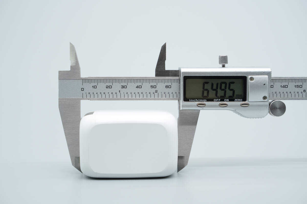
The length of the charger is about 64.95 mm (2.56 inches).
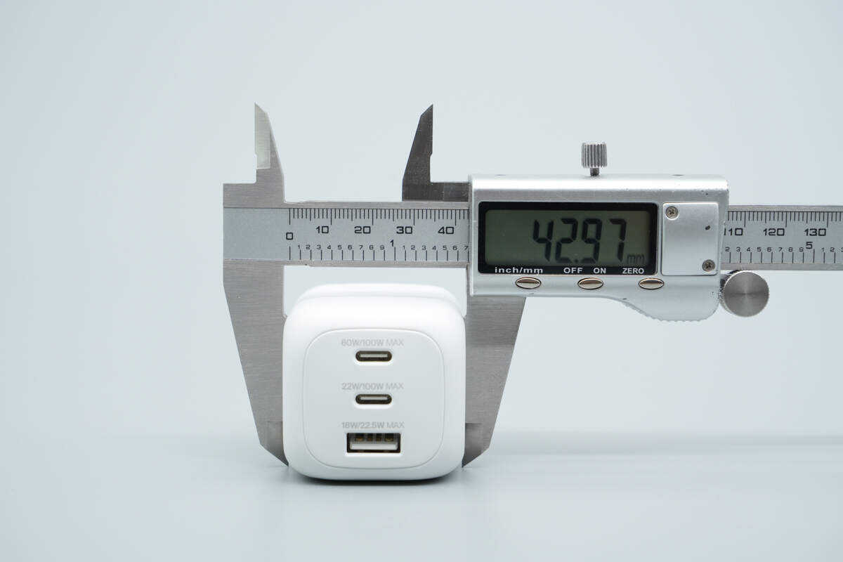
The width is about 42.97 mm (1.69 inches).

The thickness is about 42.78 mm (1.68 inches).
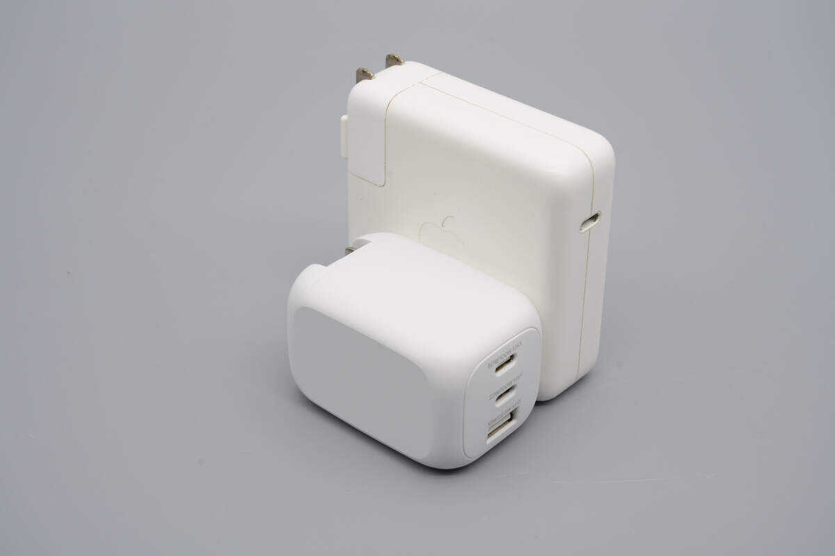
It is much smaller in size compared to the Apple 96W charger.

That's how big it is in the hand.
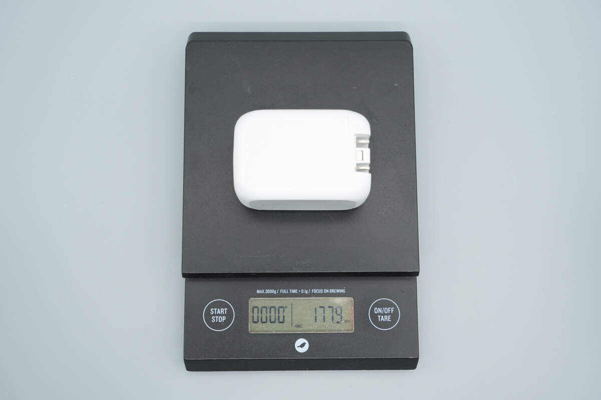
The weight is about 178 g (26.28 oz).

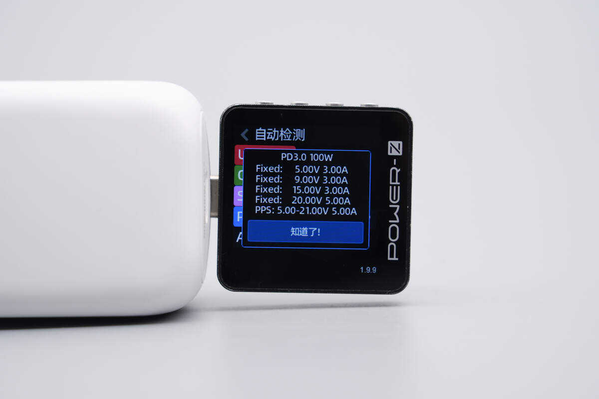
ChargerLAB POWER-Z KM003C shows that the USB-C1 supports UFCS, QC3.0/5, FCP, SCP, AFC, PD3.0, PPS, DCP, and Apple 2.4A charging protocols.
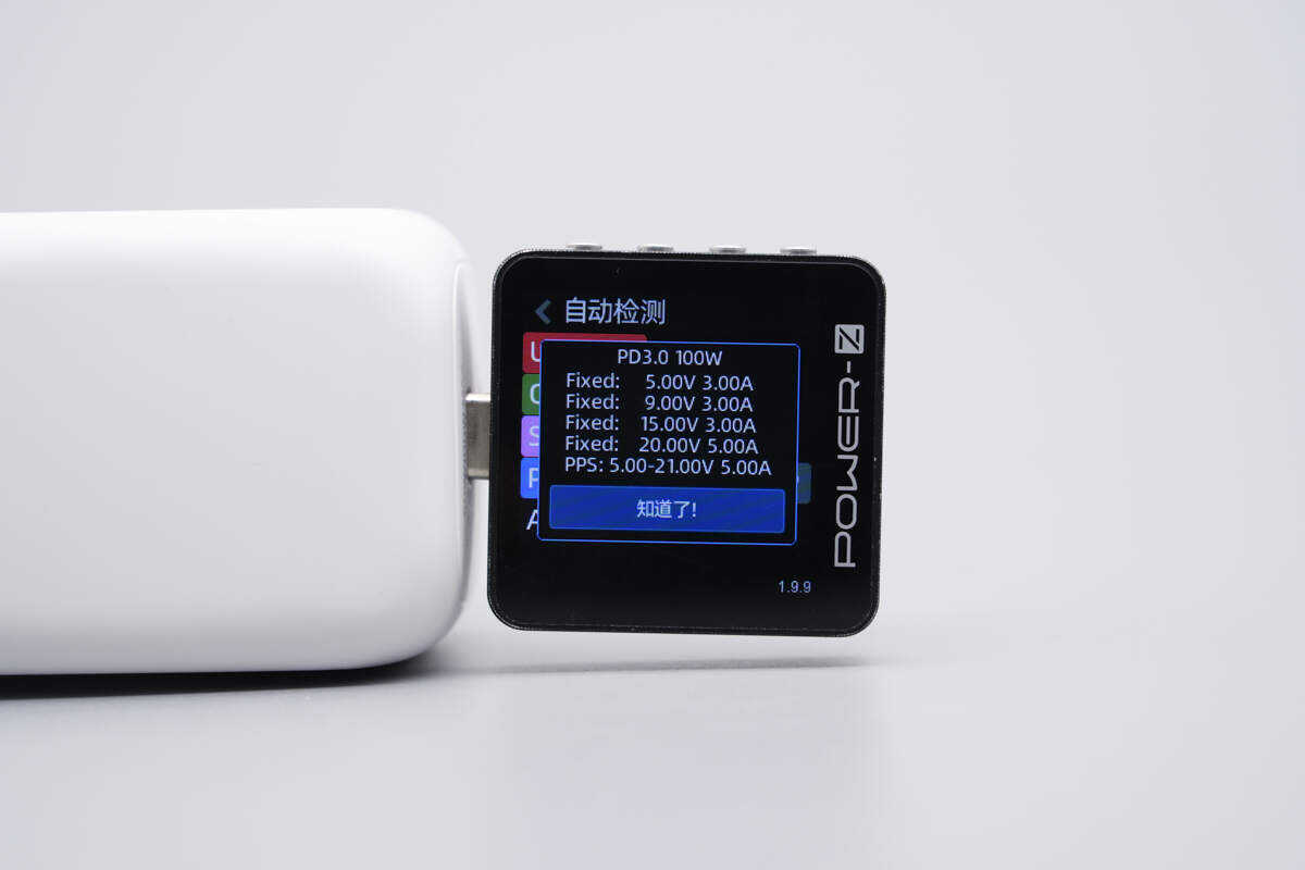
It features four fixed PDOs of 5V3A, 9V3A, 15V3A, and 20V5A. It also has one set PPS, which is 5-21V5A.
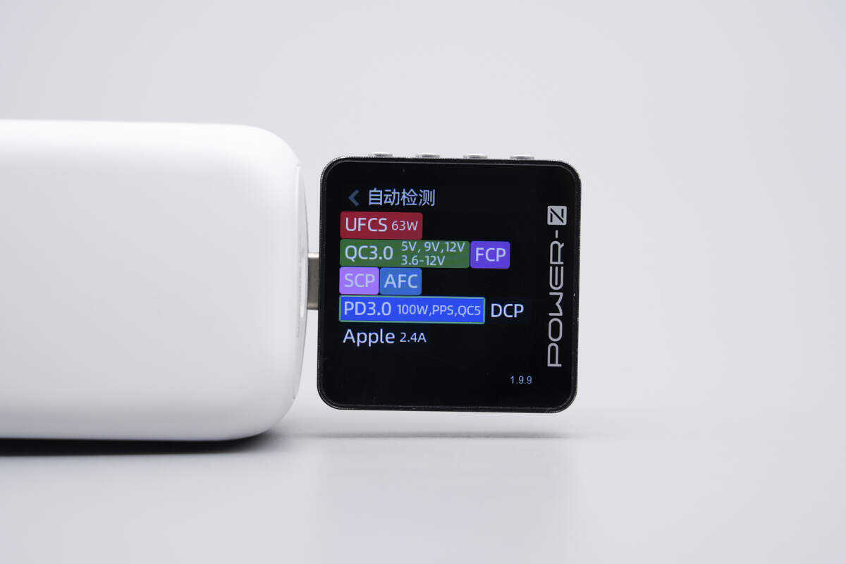
The USB-C2 port supports the same protocols as the USB-C1 port.
The PDO messages are also identical.

The USB-A supports QC3.0, FCP, SCP, AFC, DCP, and Apple 2.4A charging protocols.
Teardown
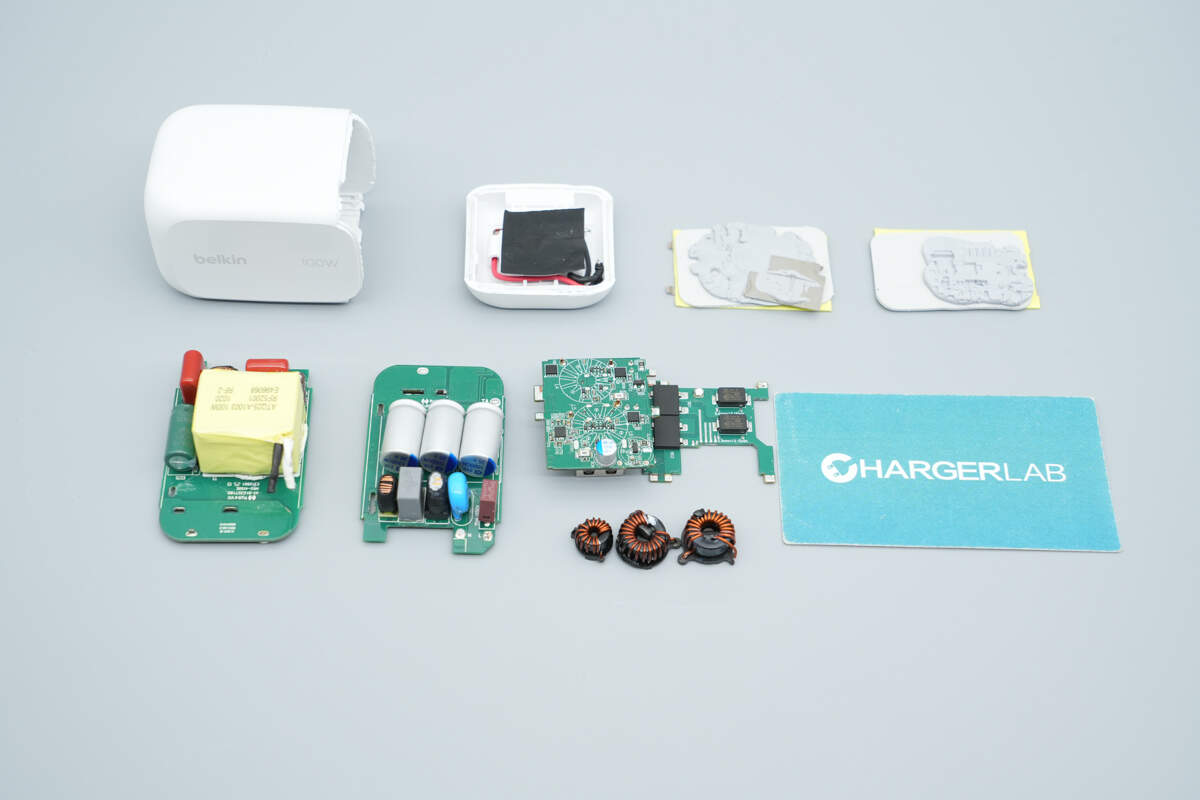
Next, let's take it apart to see its internal components and structure.
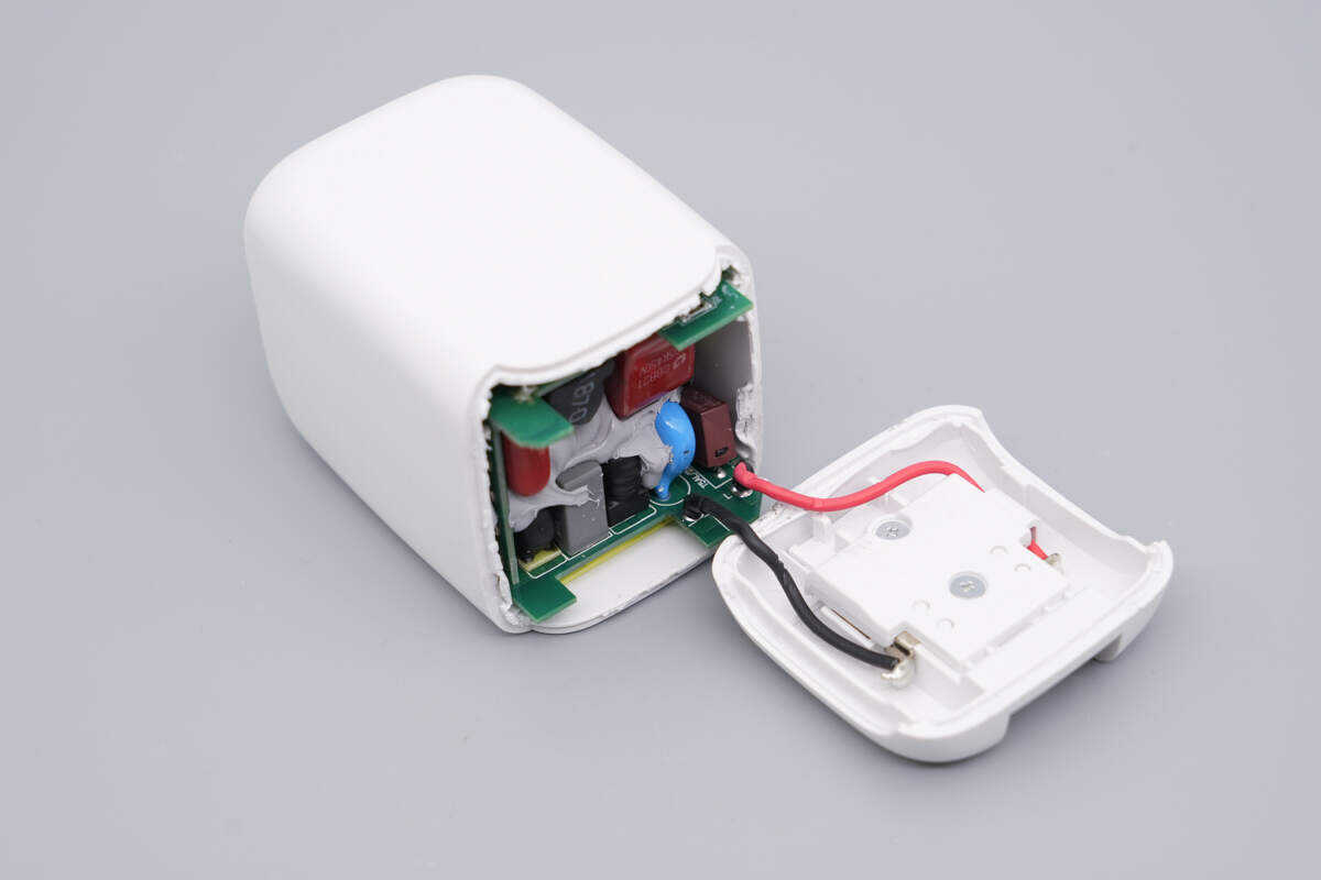
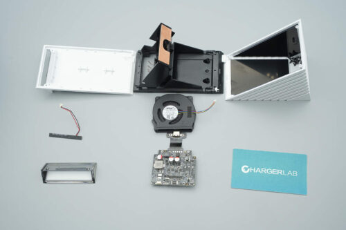
Remove the input-side housing. The plug is secured with a plastic plate and screws and is connected to the PCB via wires.
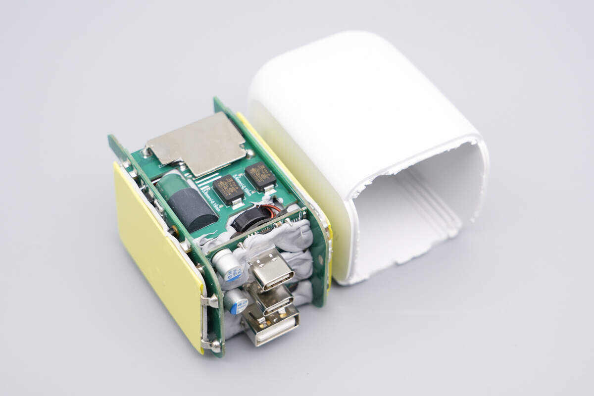
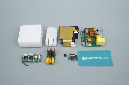
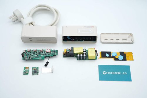
Remove the PCBA module.
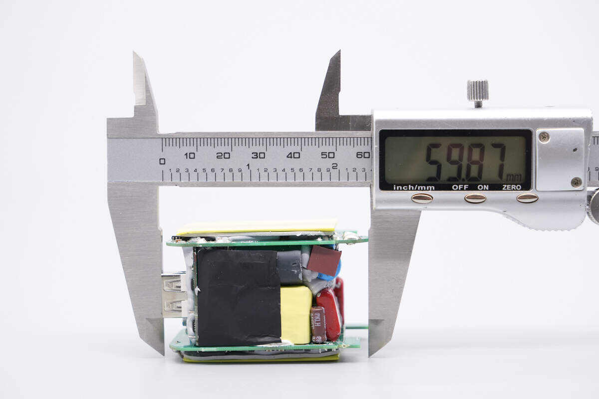
The length of the PCBA module is about 59.87 mm (2.36 inches).
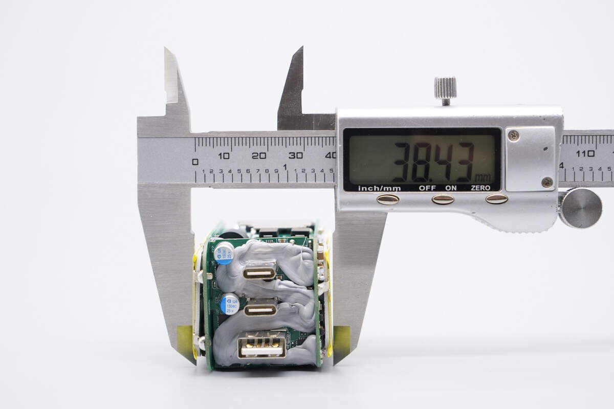
The width is about 38.43 mm (1.51 inches).
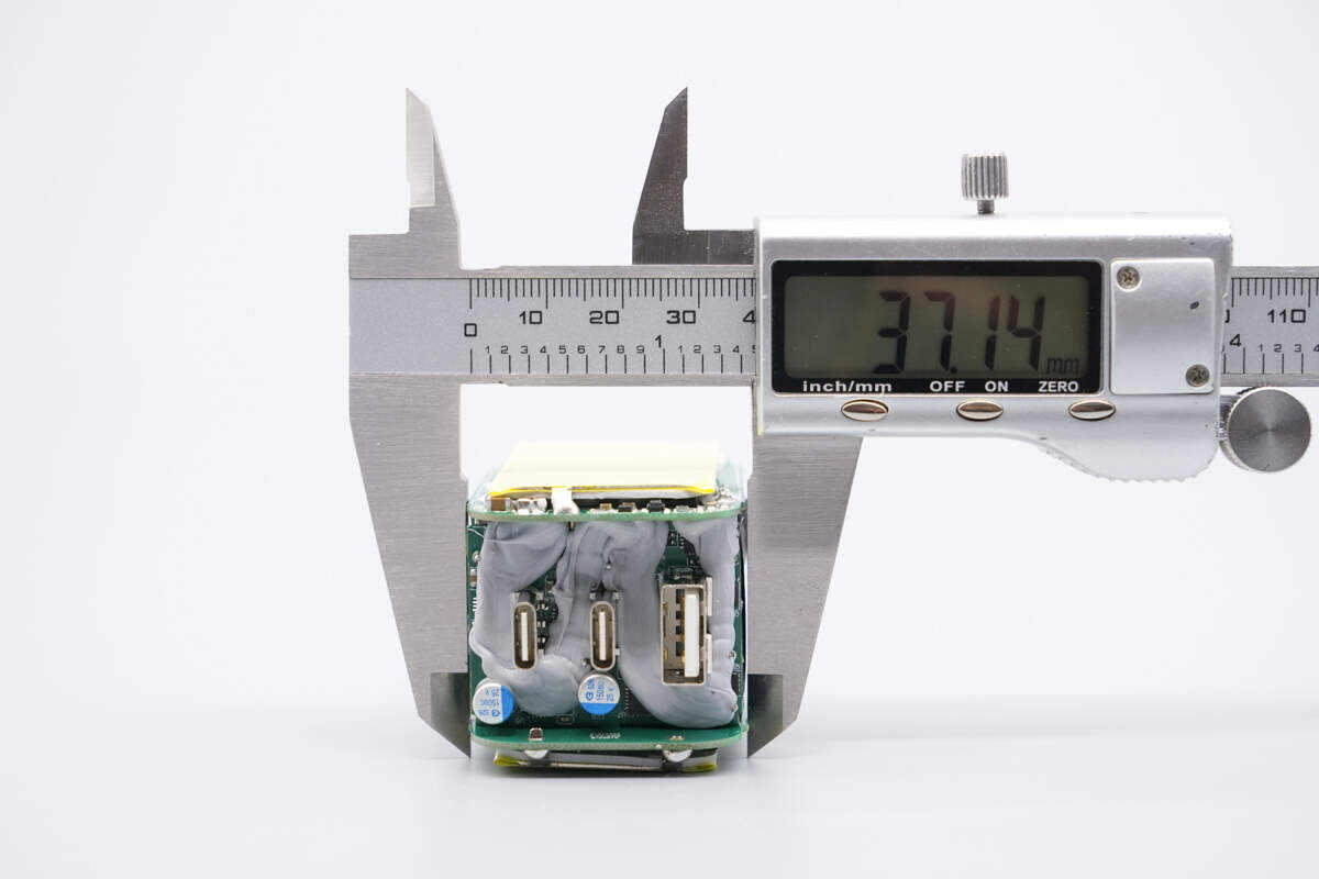
The thickness is about 37.14 mm (1.46 inches).
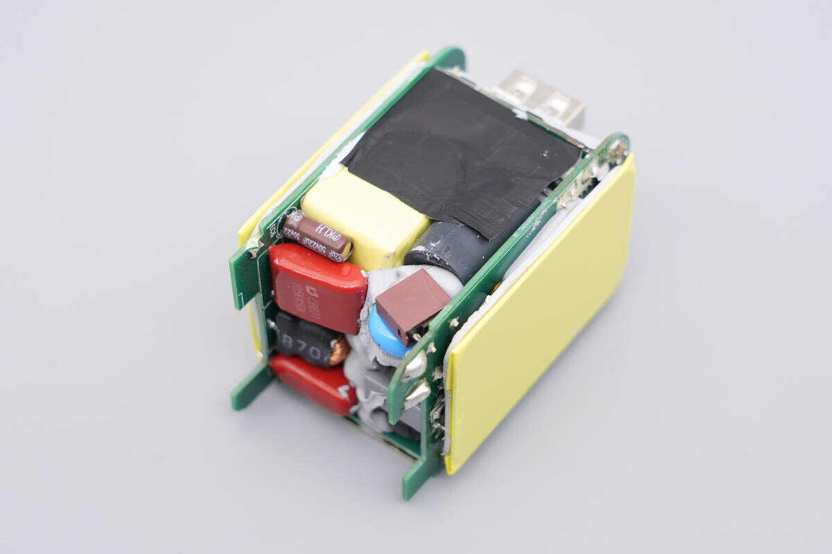
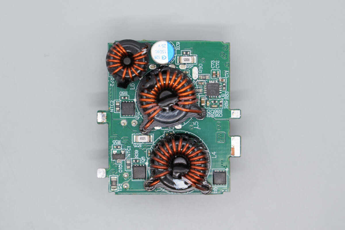
The PCBA module is stacked with four PCBs. The gaps are filled with thermal adhesive, and a graphite thermal pad is also applied. The PCBs on the sides are equipped with metal heat sinks.
The bottom PCB, corresponding to the bridge rectifier area, is equipped with a heat sink. The front side of the output PCB is coated with adhesive.
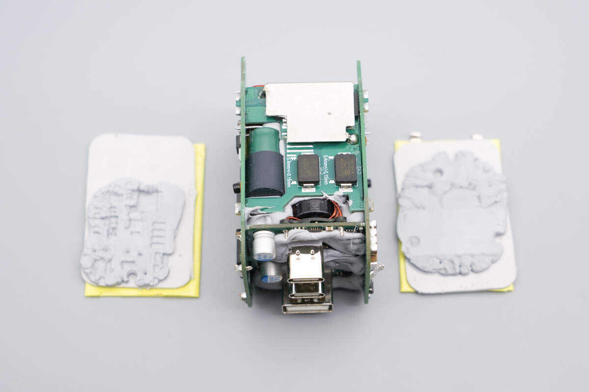
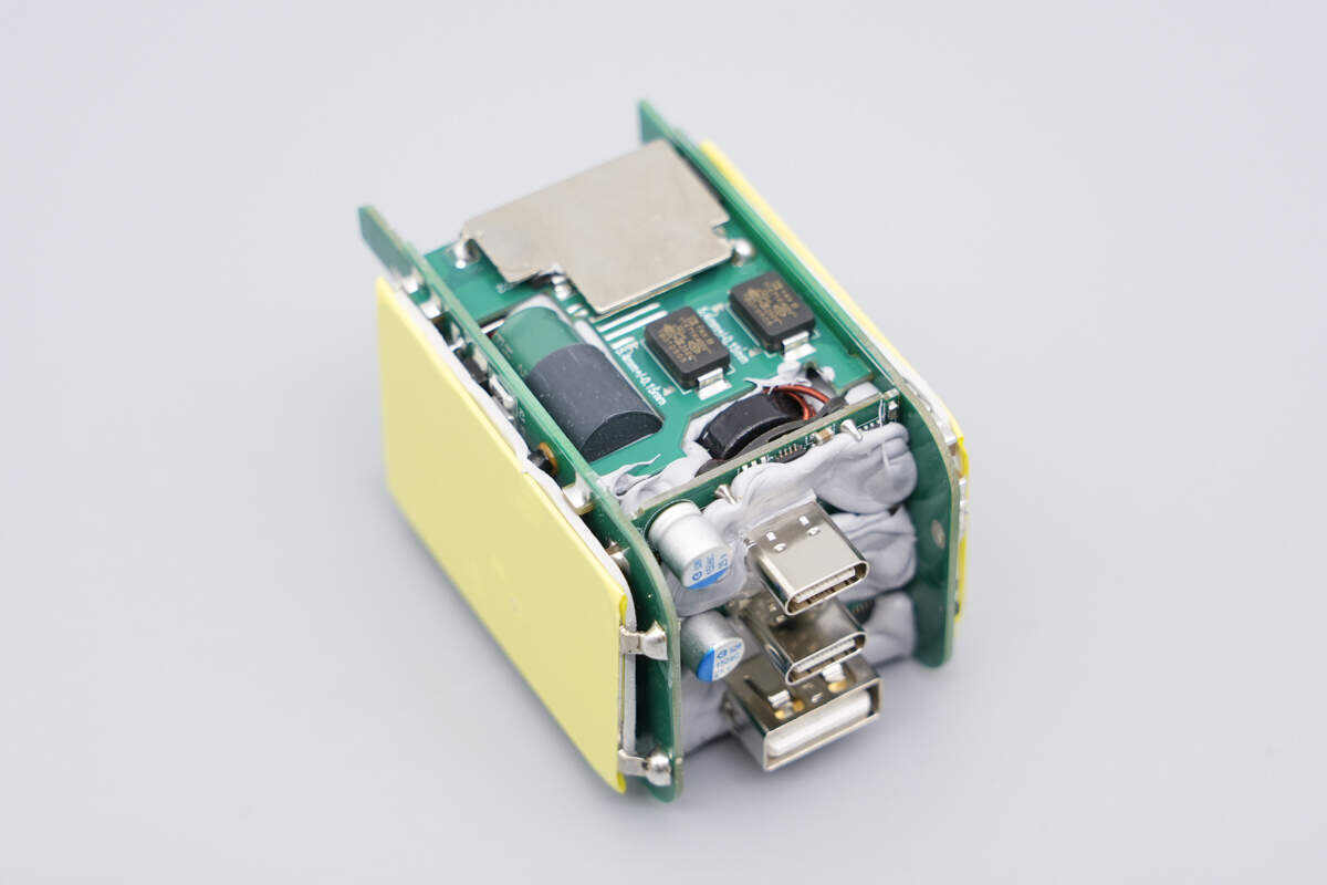
Remove the heat sinks on both sides, revealing thermal adhesive and thermal pads on the inner side.

The PCBA module is disassembled and cleaned. Both the electrolytic capacitor and the solid capacitors are covered with insulating sleeves.

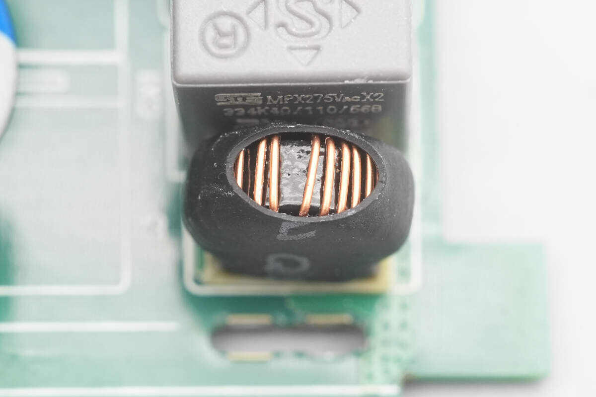
One of the side PCBs has, on its front side, a time-delay fuse, a varistor, a common-mode choke, a safety X2 capacitor, a differential-mode choke, and three solid capacitors.
On the back side, there is a synchronous rectifier controller along with the synchronous rectifiers.
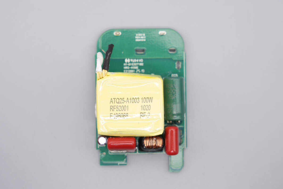
On the front side of this PCB, there are film capacitors, a filter inductor, an electrolytic capacitor, a capacitor supplying power to the master control chip, and a transformer.
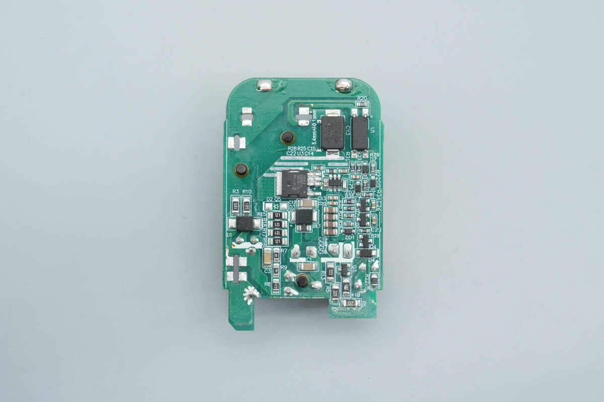
On the back side, there is the master control chip, the primary MOSFET, an optocoupler, and an SMD Y capacitor.
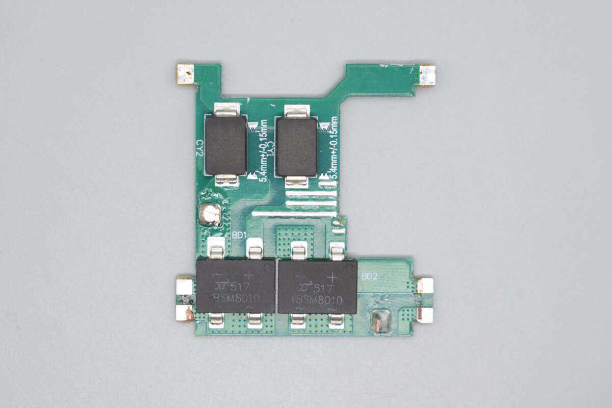
On the bottom PCB, there are two bridge rectifiers and two SMD Y capacitors.
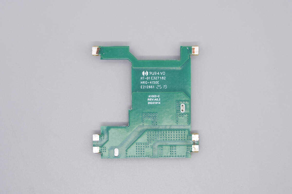
The other side has no components.
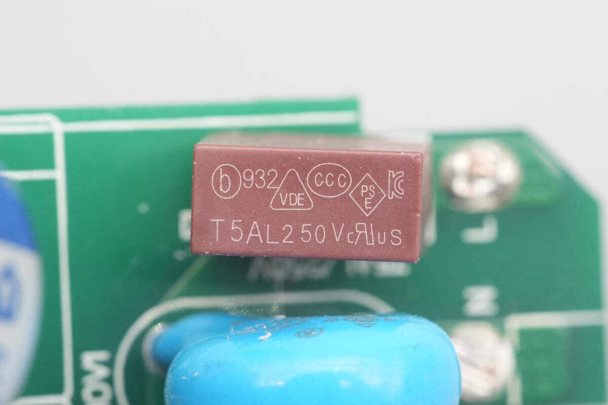
The time-delay fuse is from Betterfuse, part number 932, rated at 5A 250V.

The 10D681K varistor is from STE and is used for input overvoltage protection.
The common mode choke is used to filter EMI interference and is insulated with a heat-shrink tube for protection.
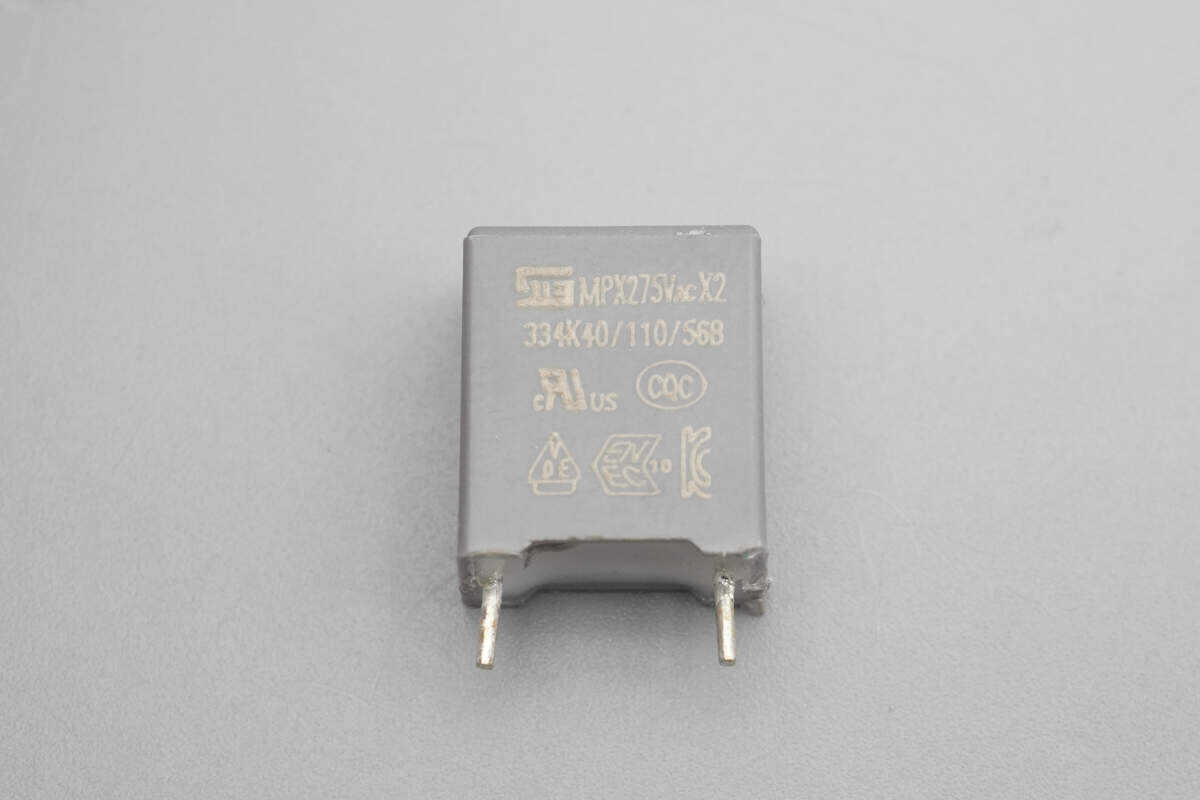
The safety X2 capacitor is also from STE, with a capacitance of 0.33 μF.
The differential mode choke is also covered with a heat-shrink tube, and a bakelite board is installed at the bottom.
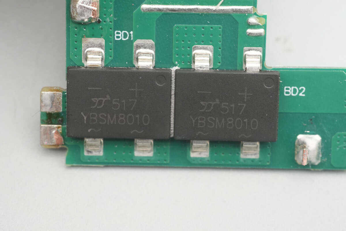
The bridge rectifiers are from YJ, model YBSM8010, rated at 8A 1000V, with two units used to share heat dissipation.
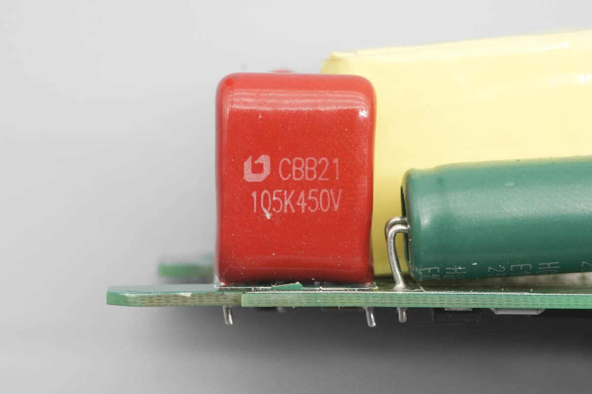
The CBB21 film capacitor is from Surong, rated at 450V 1 μF.
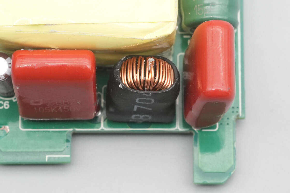
The filter inductor is protected with a heat-shrink tube.
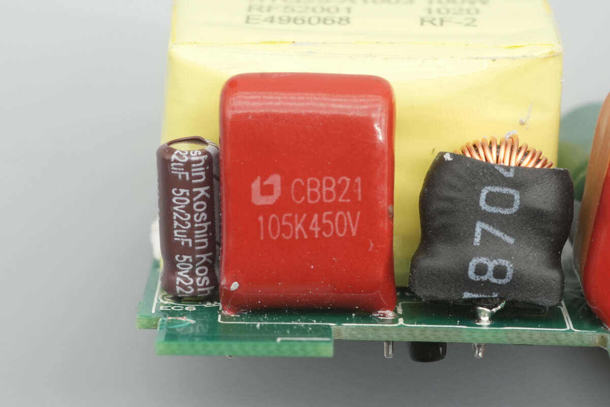
The other film capacitor has the same part number.
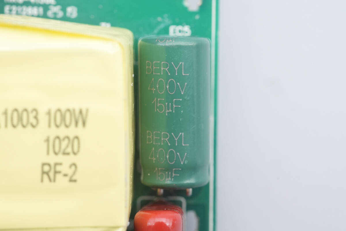
The electrolytic capacitor is from BERYL, rated at 400V 15 μF.

The primary master control chip is from RENESAS, marked with “5H,” model iW3627-00. It is a single-stage AC/DC constant-voltage controller with power factor correction, supporting both isolated and non-isolated topologies. The chip achieves very low load and line voltage regulation without requiring secondary feedback circuits, and it does not need external loop compensation components. It comes in a SOT-23 package.
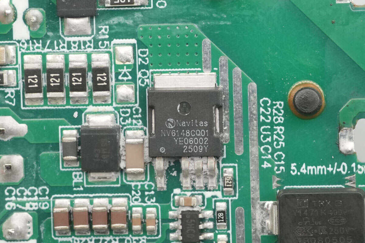
The primary MOSFET is from Navitas, model NV6148C. It is a 700V GaNSlim series power IC featuring a high-performance eMode GaN FET with an on-resistance of 120 mΩ. The IC integrates a gate driver along with multiple extended functions, aiming to deliver one of the fastest, most compact, highly efficient, and reliable power integration solutions on the market.
The NV6148C includes lossless current sensing to improve system efficiency and incorporates over-temperature protection to enhance reliability. Its automatic standby and sleep modes significantly increase efficiency under light-load and no-load conditions. Additionally, it offers very high dV/dt immunity. The device comes in a DPAK-4L package.
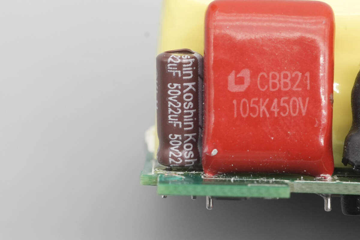
The capacitor supplying power to the master control chip is from Koshin, rated at 50V 22 μF.

The transformer uses an ATQ25 magnetic core.
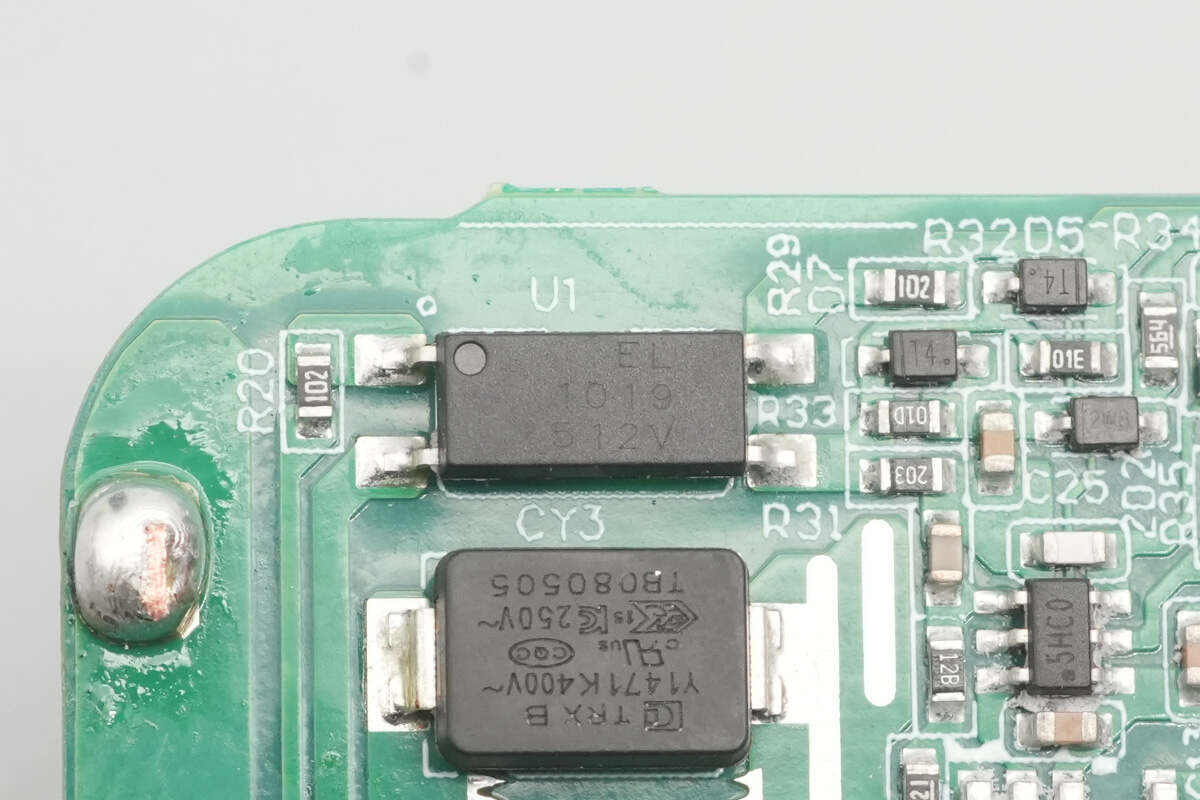
The Everlight EL1019 optocoupler is used for output voltage feedback.
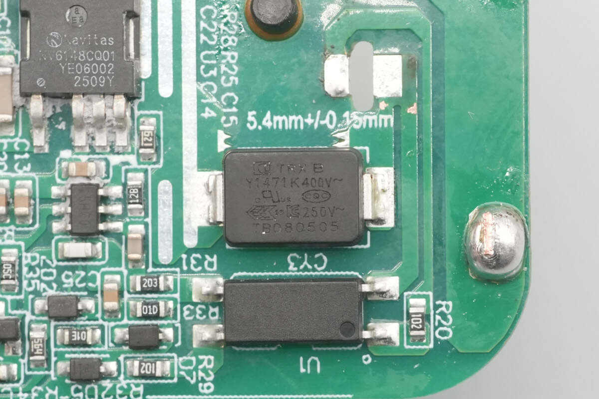
The SMD Y capacitor is from TRX, part number TMY1471K. Its compact size and light weight make it well-suited for high-density power products such as GaN fast chargers.
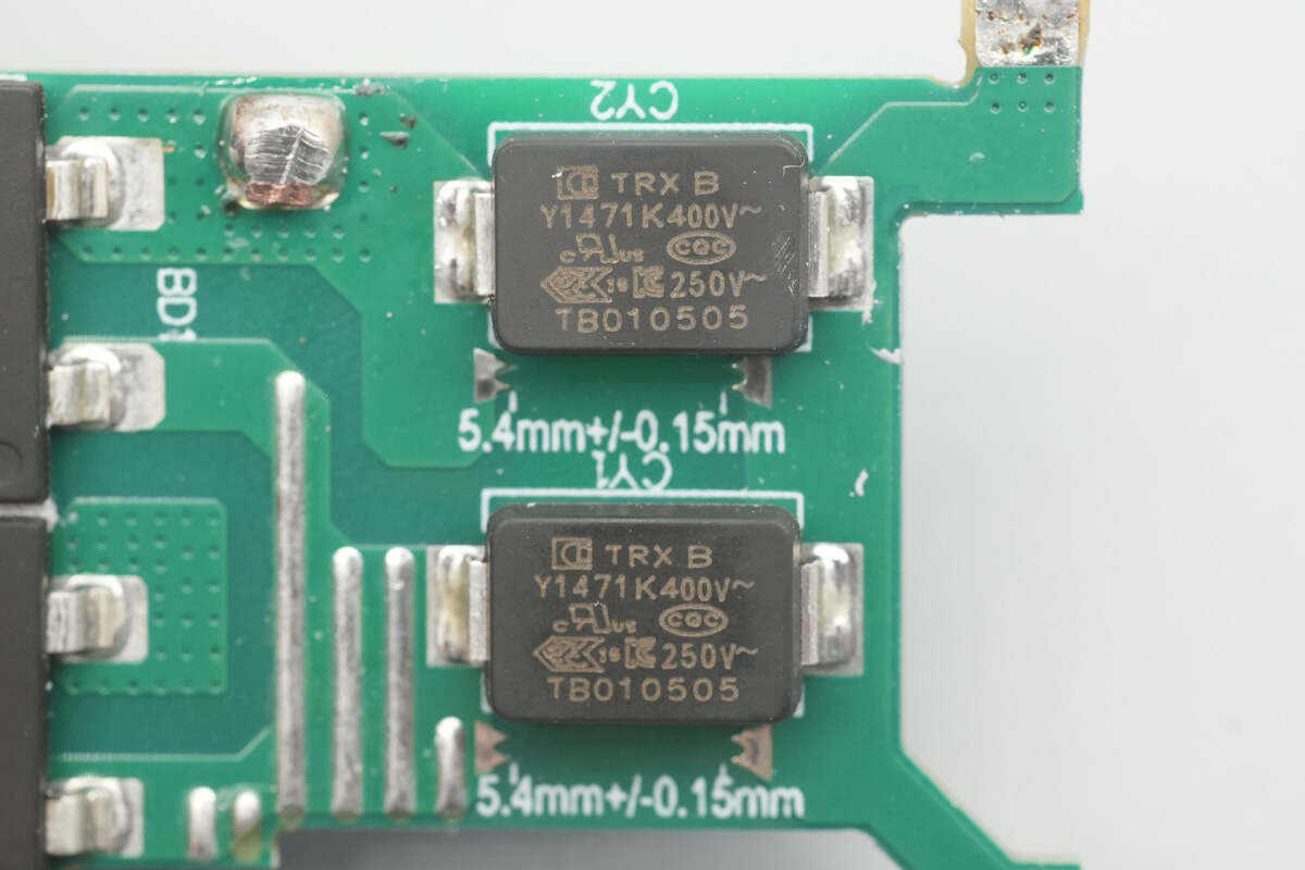
The other two SMD Y capacitors have the same part number.
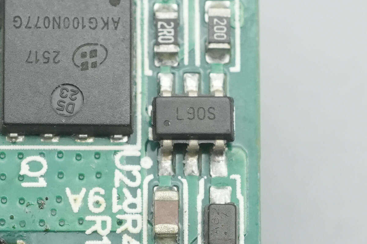
The synchronous rectifier controller is from RENESAS, marked “L9,” model iW610-01C. It supports QR, ZVS, ACF, and LLC switching power supply applications, and operates in both DCM and CCM modes. It can be used for low-side and high-side applications, supports an output voltage range of 3–28 V, and comes in a SOT-23 package.
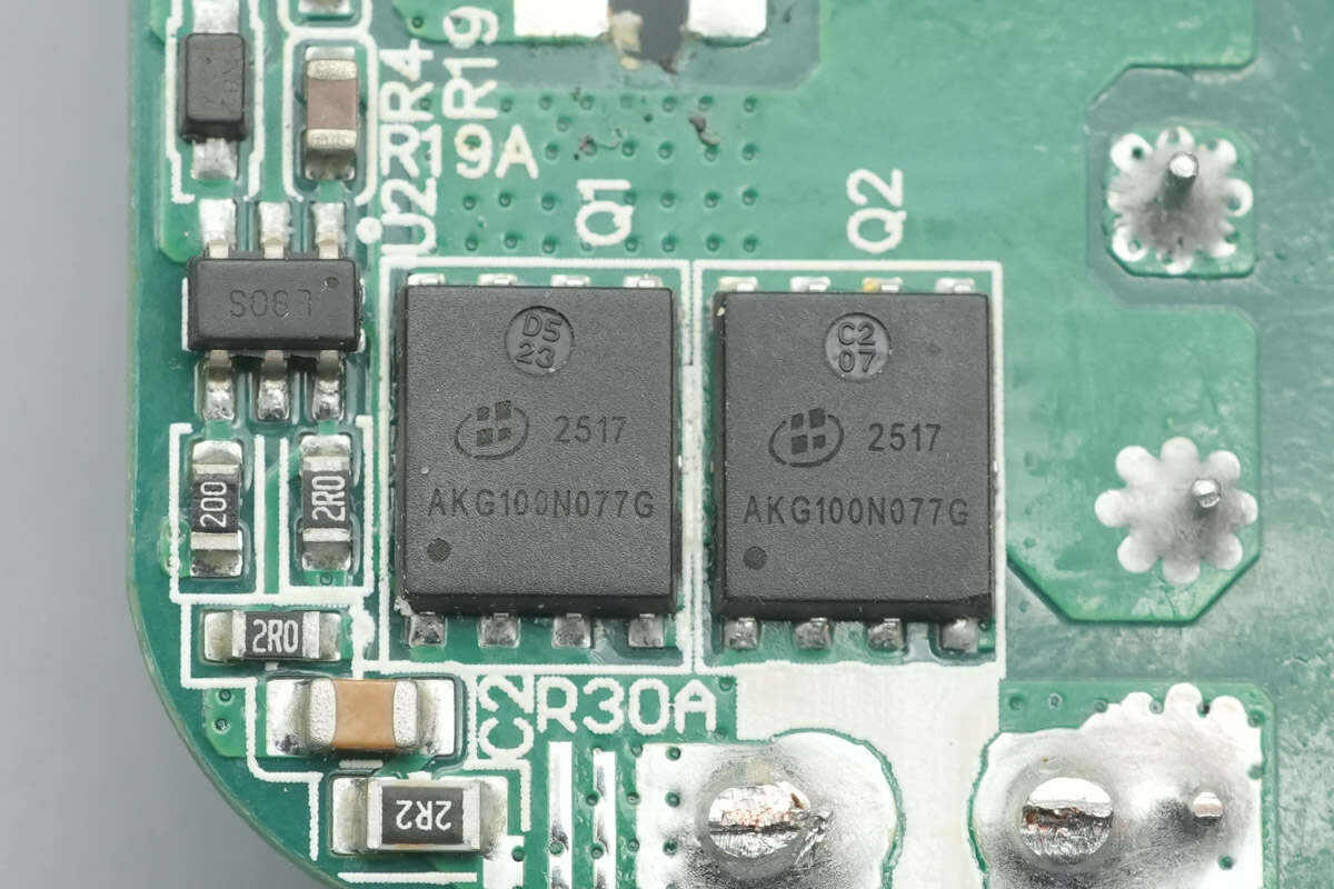
The synchronous rectifiers are from ALKAIDSEMI, model AKG100N077G. They are NMOS devices rated at 100 V with an on-resistance of 7.7 mΩ, and come in a PDFN 5×6-8L package.

The three solid capacitors are from BERYL, each rated at 35 V 1000 μF.
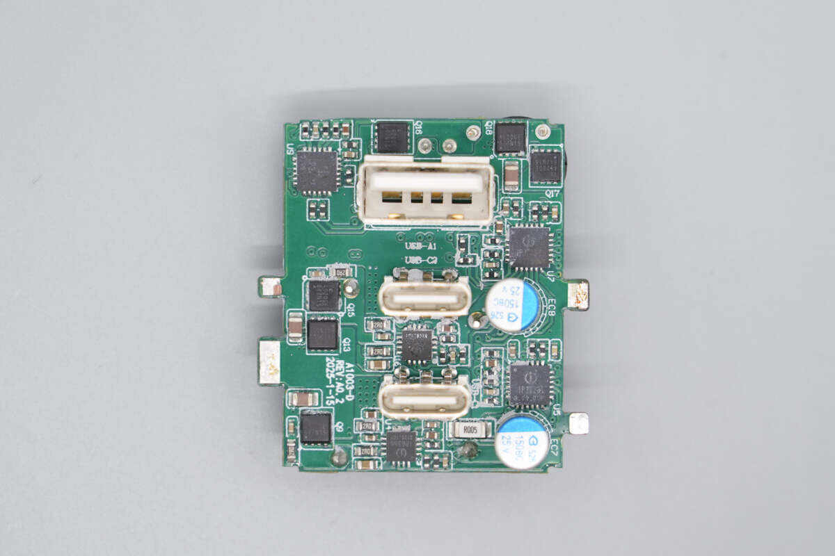
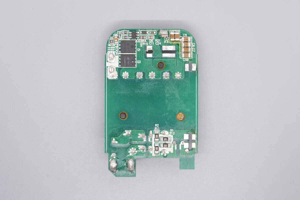
On the front side of the output PCB, there are synchronous buck controllers, synchronous buck MOSFETs, solid capacitors, protocol chips, and a VBUS MOSFET.
On the back side, there are a synchronous buck controller, synchronous buck MOSFETs, buck inductors, a solid capacitor, and VBUS MOSFETs.
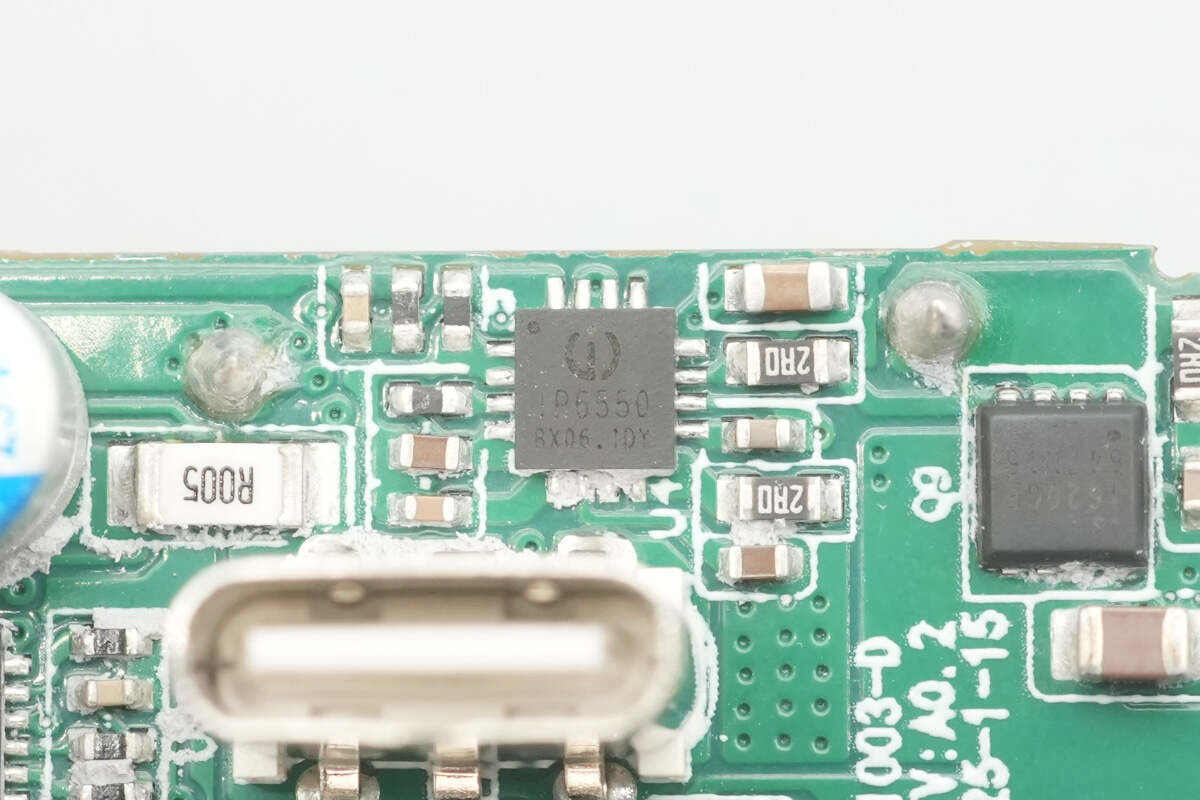
The synchronous buck controller for the USB-C1 port is from Injoinic, model IP6550. It supports 36 V input, features a built-in NMOS driver, and uses two external MOSFETs for efficient synchronous buck conversion. The switching frequency is 135 kHz, the input voltage rating is 48 V, and it includes comprehensive protection features. It comes in a 3×3 mm QFN16 package.
The IP6550 can be used in car chargers, multi-port adapters, smart power strips, USB-C–enabled power strips, and dashcam applications. Its synchronous buck design offers high conversion efficiency and supports high output currents for multiple 5 V outputs. When paired with a PD protocol chip, it enables wide-range voltage regulation, meeting the requirements of USB PD3.1 applications.
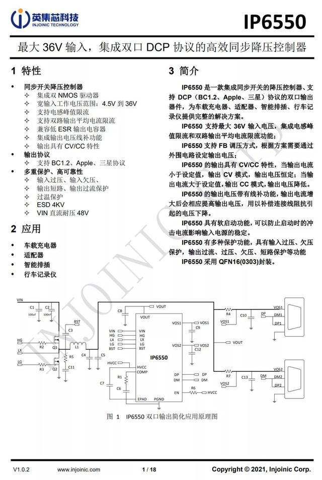
Here is the information about Injoinic IP6550.
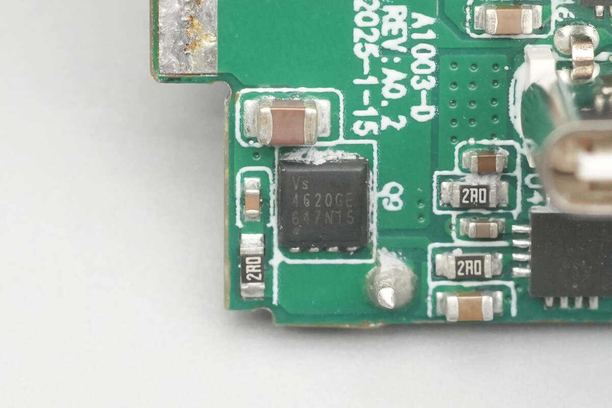
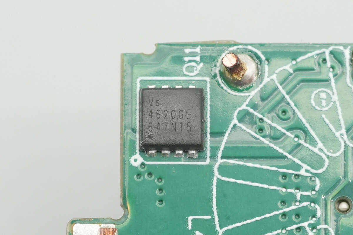
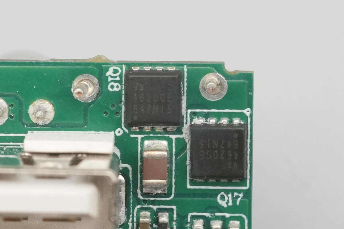
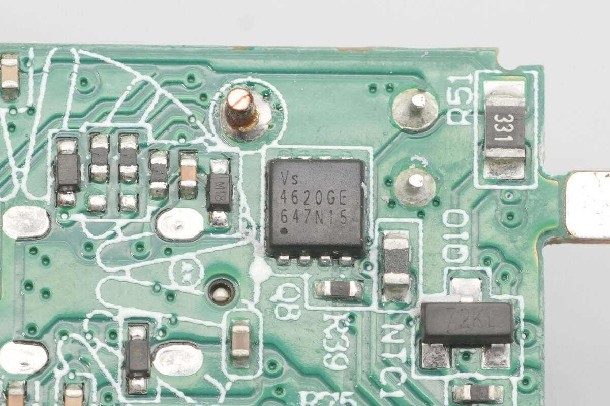
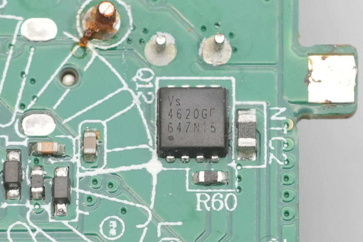
The synchronous buck MOSFET is from Vergiga, model VS4620GEMC. It is an NMOS device rated at 40 V with an on-resistance of 6.4 mΩ, and comes in a PDFN3333 package.
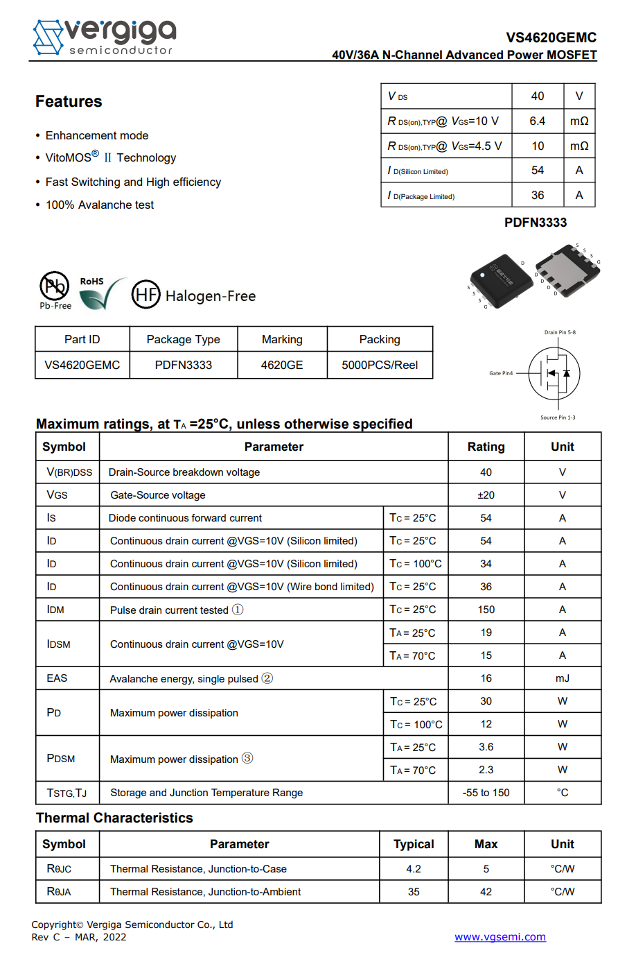
Here is the information about Vergiga VS4620GEMC.
The other Vergiga VS4620GEMC synchronous buck MOSFET is located on the back side of the PCB.

The synchronous buck controller for the USB-C2 port also uses the Injoinic IP6550.
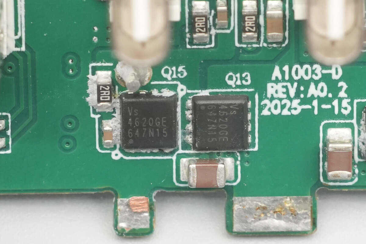
These two synchronous buck MOSFETs are also Vergiga VS4620GEMC.
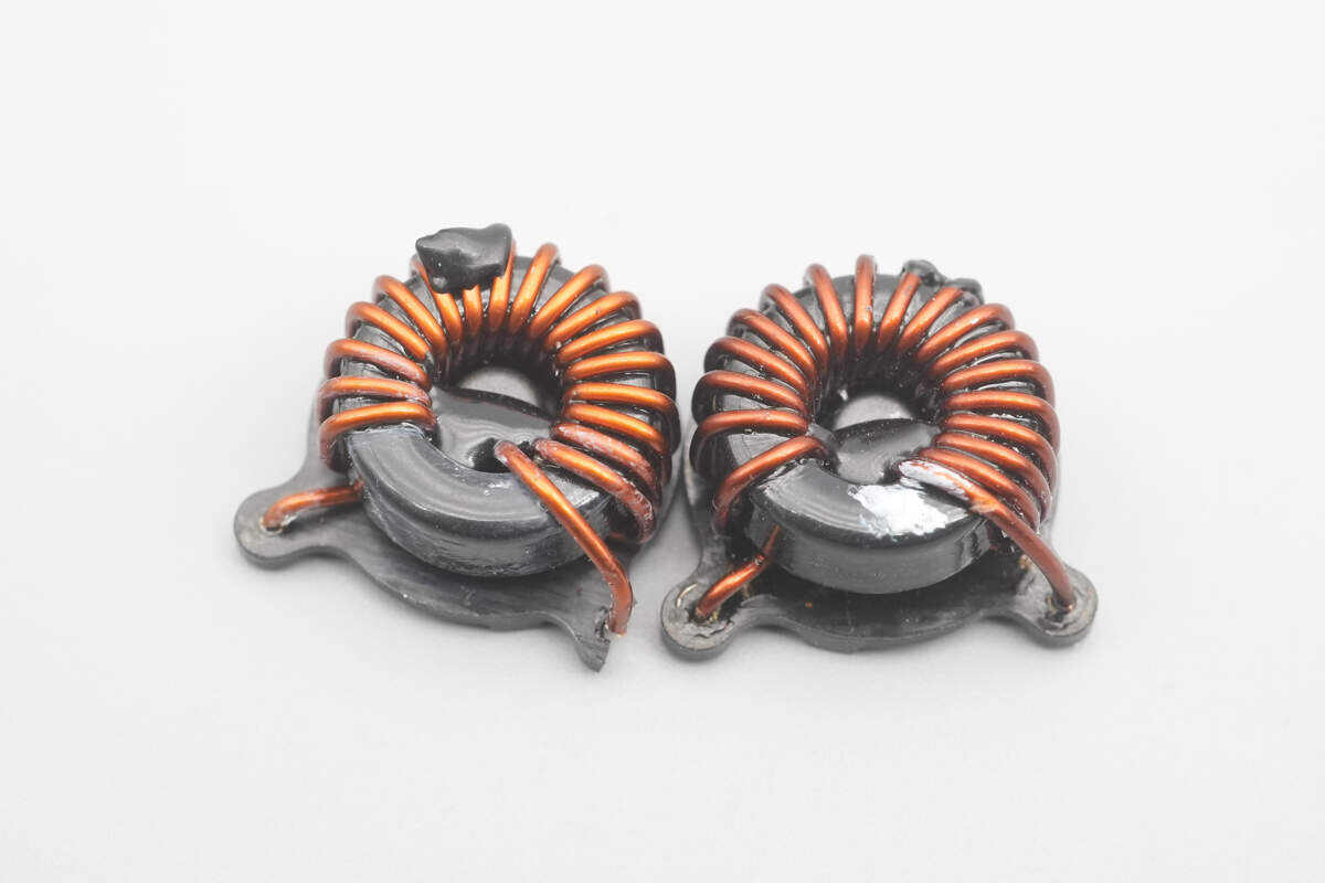
The buck inductors have plastic plates at the bottom, with the center reinforced using adhesive.
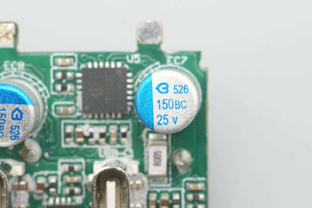
The solid capacitor for the secondary buck output filter is from BERYL, rated at 25 V 150 μF.
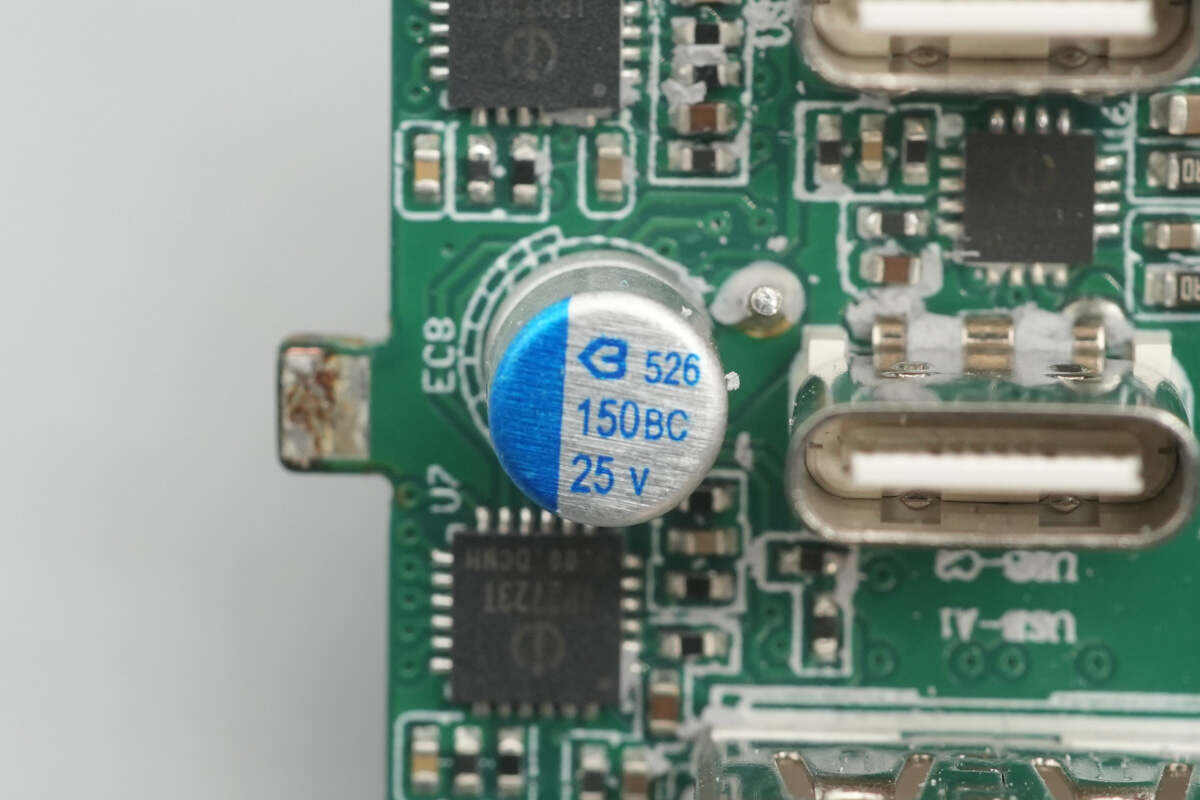
The other solid capacitor has the same part number.

The synchronous buck controller for the USB-A port also uses the Injoinic IP6550.
These two synchronous buck MOSFETs are also Vergiga VS4620GEMC.

A close-up view of the third buck inductor.
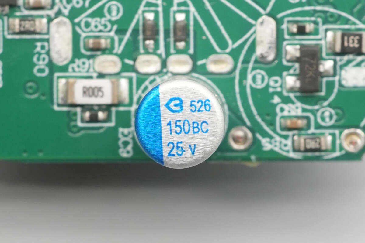
This solid capacitor is from BERYL, rated at 25 V 150 μF.
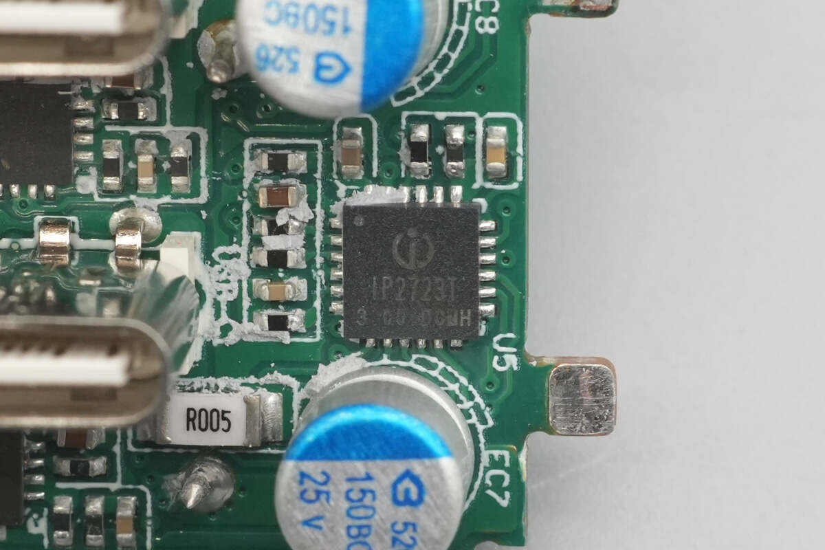
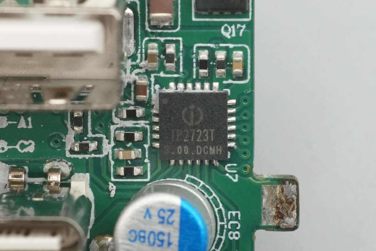
The protocol chip for the USB-C1 port is from Injoinic, model IP2723T. It is USB-IF PD3.0 PPS certified, TID: 3135, and is an integrated fast-charging protocol IC for USB output ports. It supports multiple fast-charging protocols, including USB Type-C DFP, PD2.0/3.0, PPS, HVDCP QC4, QC4+, QC3.0/2.0, FCP, SCP, AFC, MTK PE+ 2.0/1.1, Apple 2.4 A, BC1.2, and Samsung 2.0 A. On the right side of the USB-C female port, a TVS diode provides electrostatic protection.
It offers a complete Type-C solution for unidirectional output applications such as adapters and car chargers. The IP2723T is highly integrated and feature-rich, requiring minimal external components, which helps reduce overall design size and lower BOM costs.
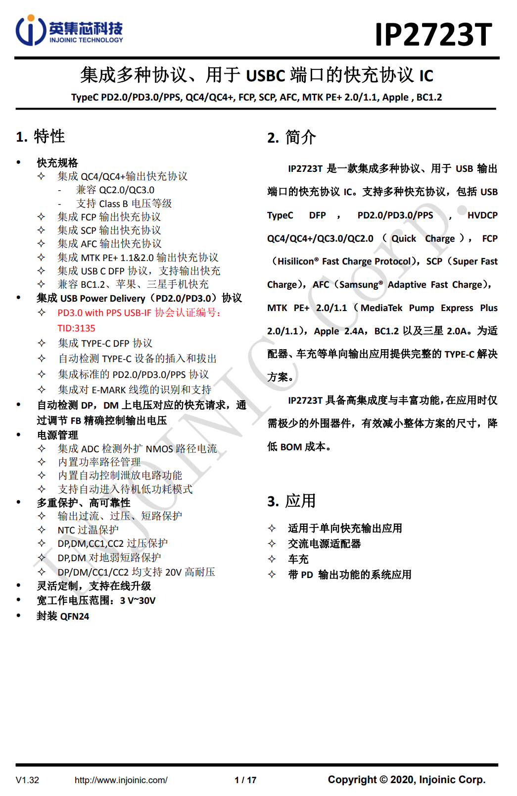
Here is the information about Injoinic IP2723T.
The protocol chip for the USB-C2 port also uses the Injoinic IP2723T.
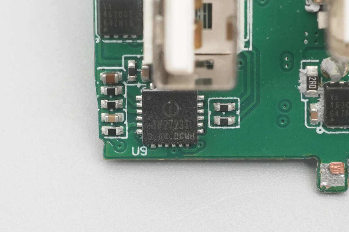
The protocol chip for the USB-A port also uses the Injoinic IP2723T.
The VBUS MOSFET for the USB-C1 port also uses the Vergiga VS4620GEMC.
The VBUS MOSFET for the USB-C2 port also uses the Vergiga VS4620GEMC.
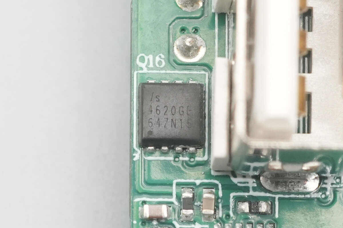
The VBUS MOSFET for the USB-A port also uses the Vergiga VS4620GEMC.
Well, those are all components of the Belkin BoostCharge Pro 100W 3-Port GaN Wall Charger.
Summary of ChargerLAB
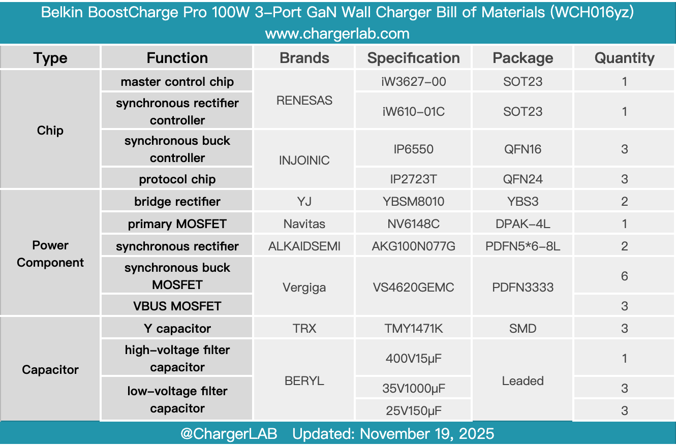
Here is the component list of the Belkin BoostCharge Pro 100W 3-Port GaN Wall Charger for your convenience.
Its enclosure is made of recycled plastic. The plug features a detachable design, allowing different plug types to be installed for use in various countries and regions. Both USB-C ports support up to 100 W output, while the USB-A port supports 22.5 W output, and it is compatible with protocols such as UFCS, PD, PPS, and SCP.
After taking it apart, we found that it uses a RENESAS iW3627-00 + iW610-01C single-stage high-PF power supply architecture and a Navitas NV6148C GaN device. The PCBA module consists of four stacked PCBs to optimize space utilization.
The output side features three independent DC-DC secondary buck circuits, all implemented identically. Each uses an Injoinic IP6550 synchronous buck controller paired with Vergiga VS4620GEMC MOSFETs for voltage conversion, with an Injoinic IP2723T protocol chip managing the interface output. All capacitors are from BERYL. The module is cooled with heat sinks and thermal adhesive, and the build quality and material selection are reliable.
Related Articles:
1. Teardown of HONOR CHOICE 100W 20000mAh Power Bank (QHL-PB06)
2. Teardown of realme 45W Cabled Power Bank (RMC2501)
3. Teardown of Belkin BoostCharge 45W GaN Wall Charger – Spider-Man Limited Edition (WCA013yz)