Introduction
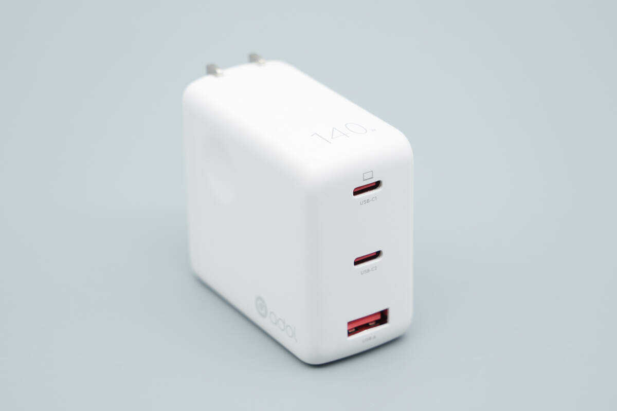
This issue presents a teardown of the ASUS Adol 140W GaN charger. The overall design is largely consistent with the previously disassembled 100W version, but while the power output has been increased, the size has grown only slightly. The charger is equipped with two USB-C ports and one USB-A port, and both USB-C ports support 140W PD 3.1 as well as Xiaomi’s 120W fast-charging protocol. The following provides a closer look at this product.
Product Appearance
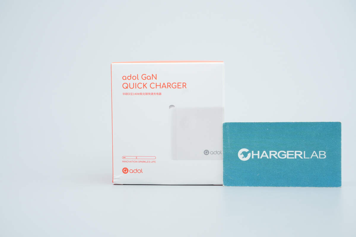
The front of the packaging box features the Adol logo, the product name, and an image of the charger.
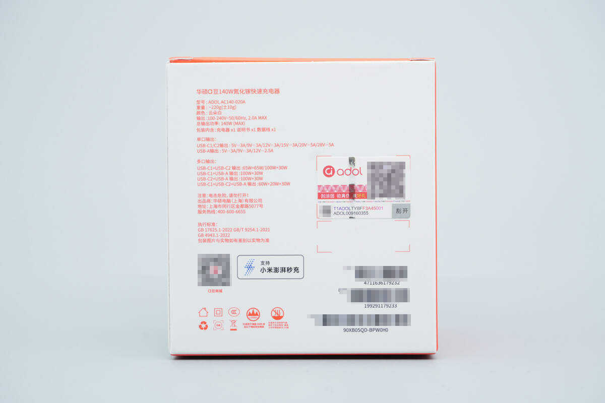
The back side lists the product specifications, safety information, and certification details.
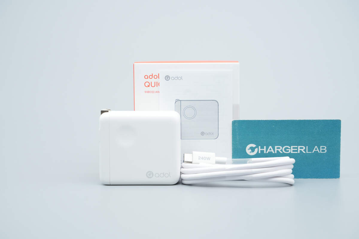
The package includes the charger, a data cable, and the user manual.
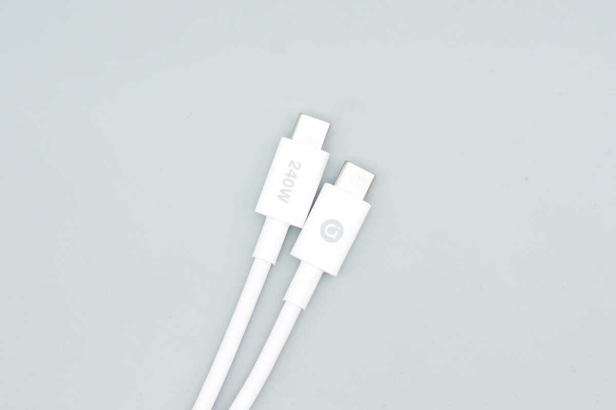
The included cable is a dual USB-C type, with the connector housings printed with the Adol logo on one end and “240W” on the other.
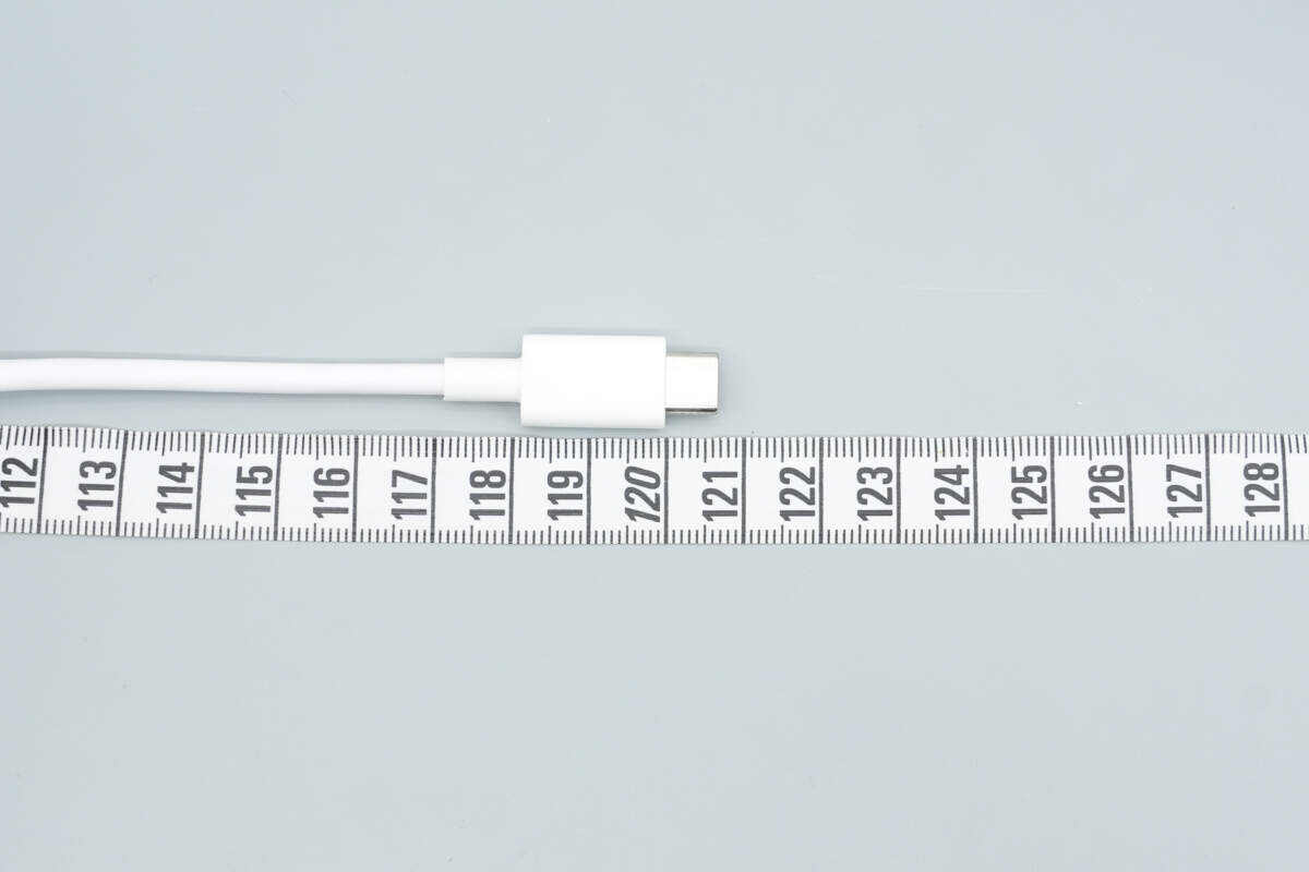
The length of the cable is about 120.5 cm (47.44 inches).
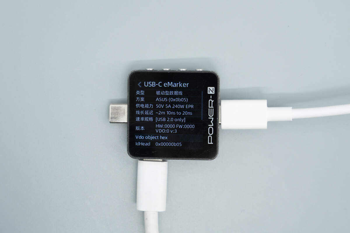
ChargerLAB POWER-Z KM003C shows it has an E-Marker chip. Its power transmission capability is 50V5A, and its data transmission capability is USB 2.0.
The enclosure is made of flame-retardant PC material and follows the same design language as the 100W version.
The front side features the Adol logo.
Both the front and back sides have grooves designed for easy plugging and unplugging.
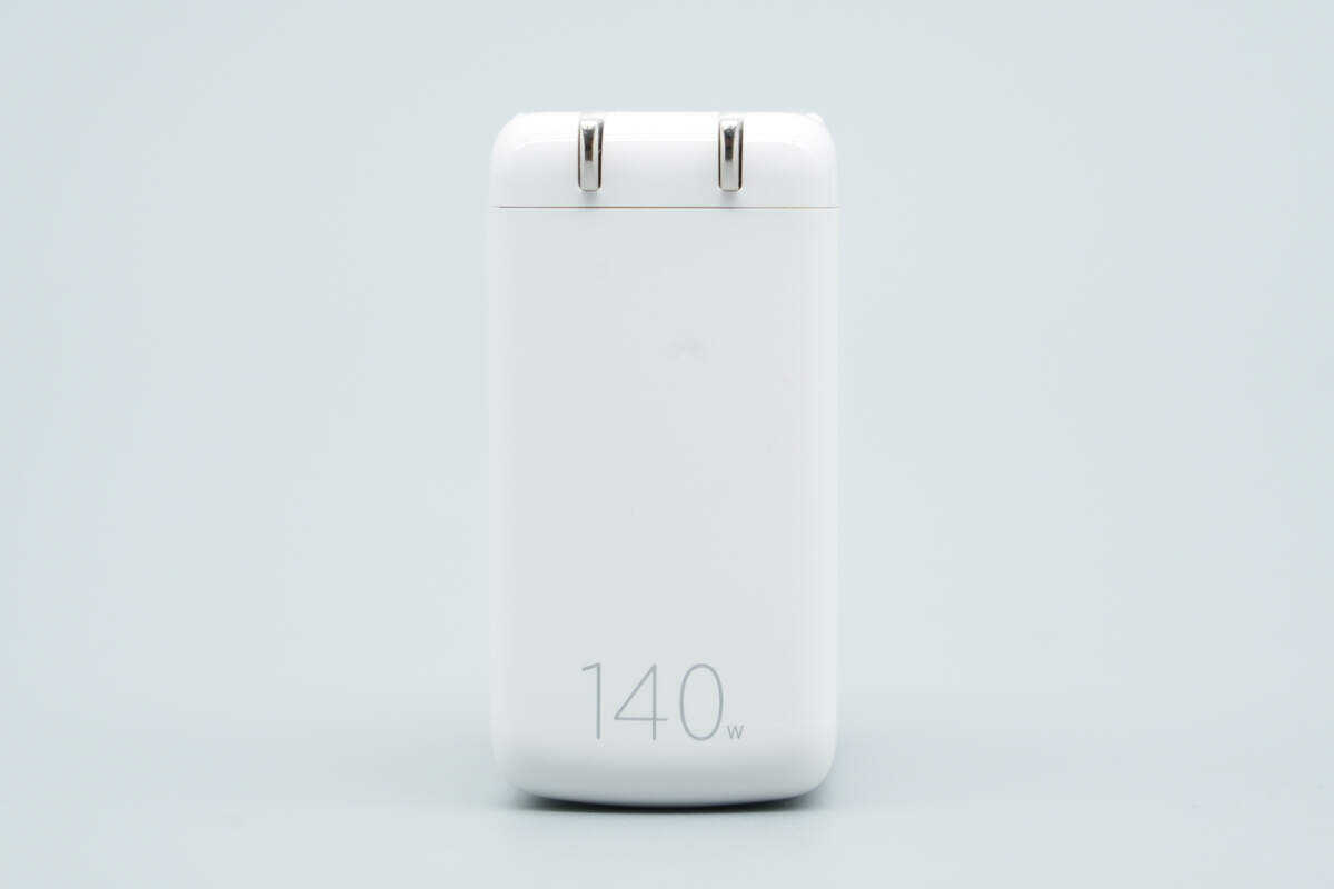
This side is marked with "140W".
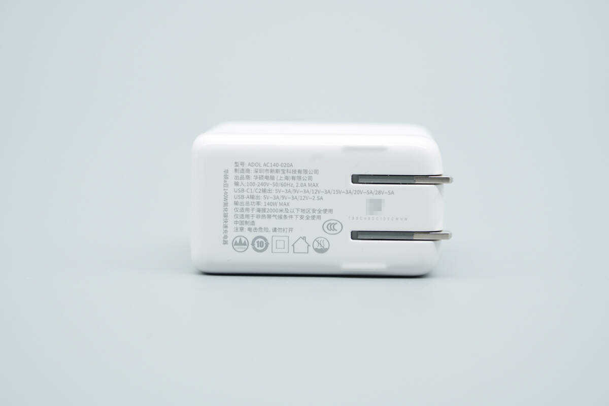
The input port housing is marked with the specifications.
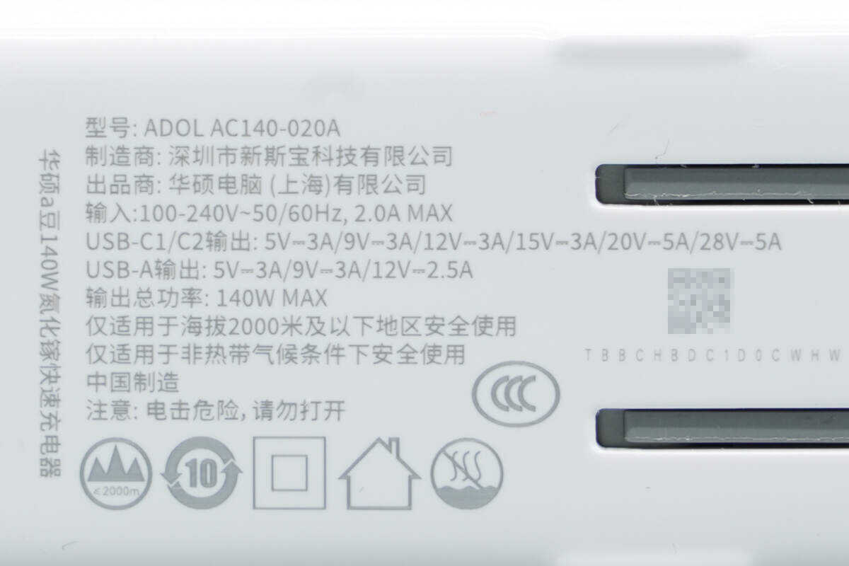
Model: Adol AC140-020A
Input: 100–240V~ 50/60Hz 2A Max
Output:
USB-C1/C2: 5V 3A, 9V 3A, 12V 3A, 15V 3A, 20V 5A, 28V 5A
USB-A: 5V 3A, 9V 3A, 12V 2.5A
Total Output Power: 140W Max
The charger is CCC certified.
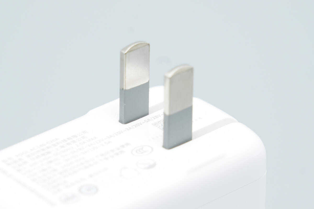
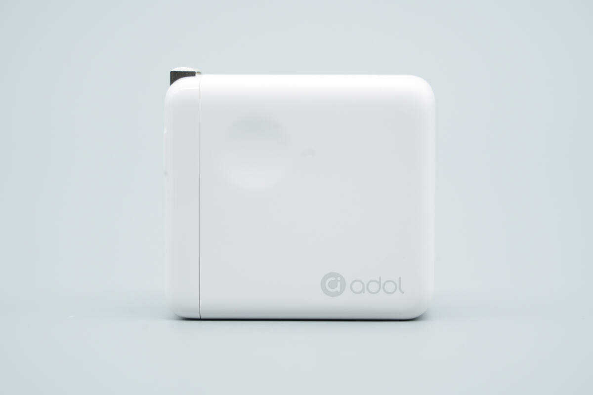
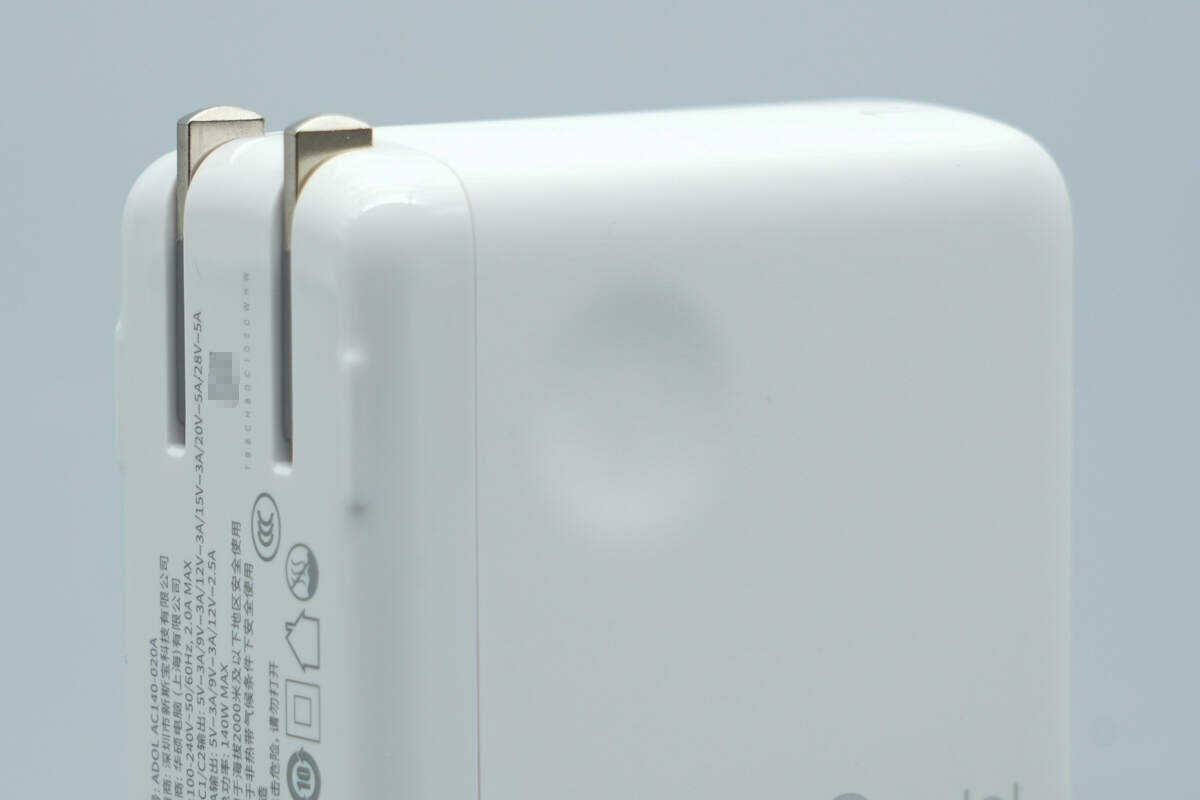
The charger comes with a foldable plug.
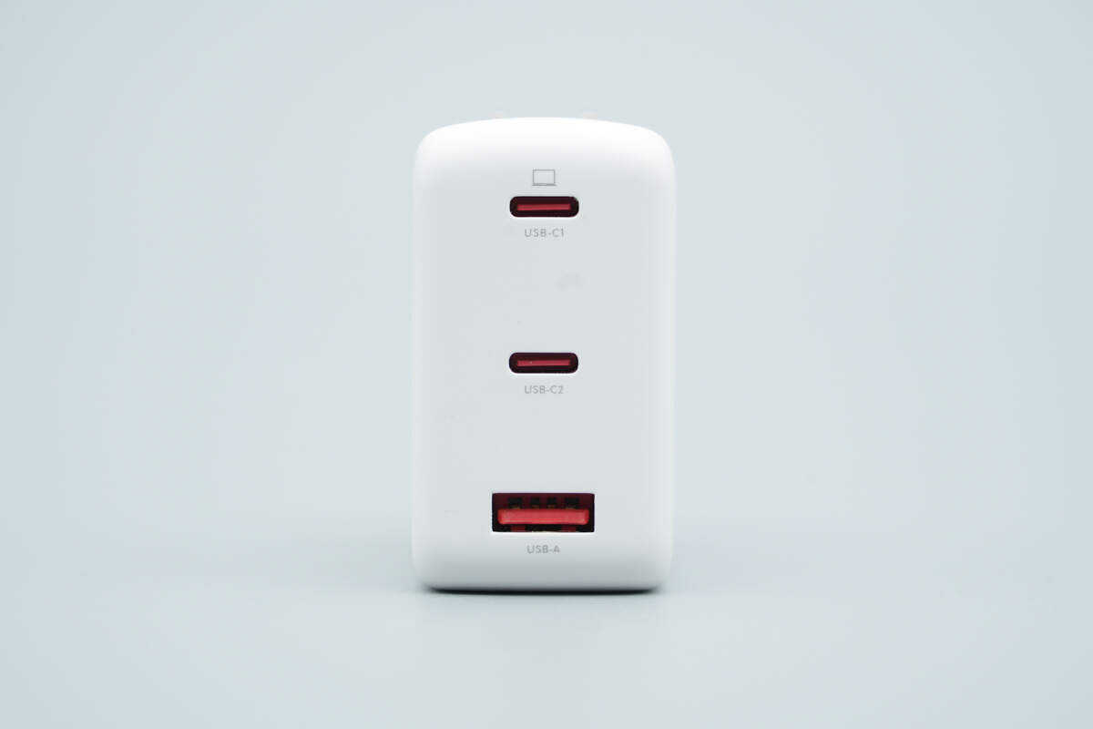
Equipped with two USB-C ports and one USB-A port.
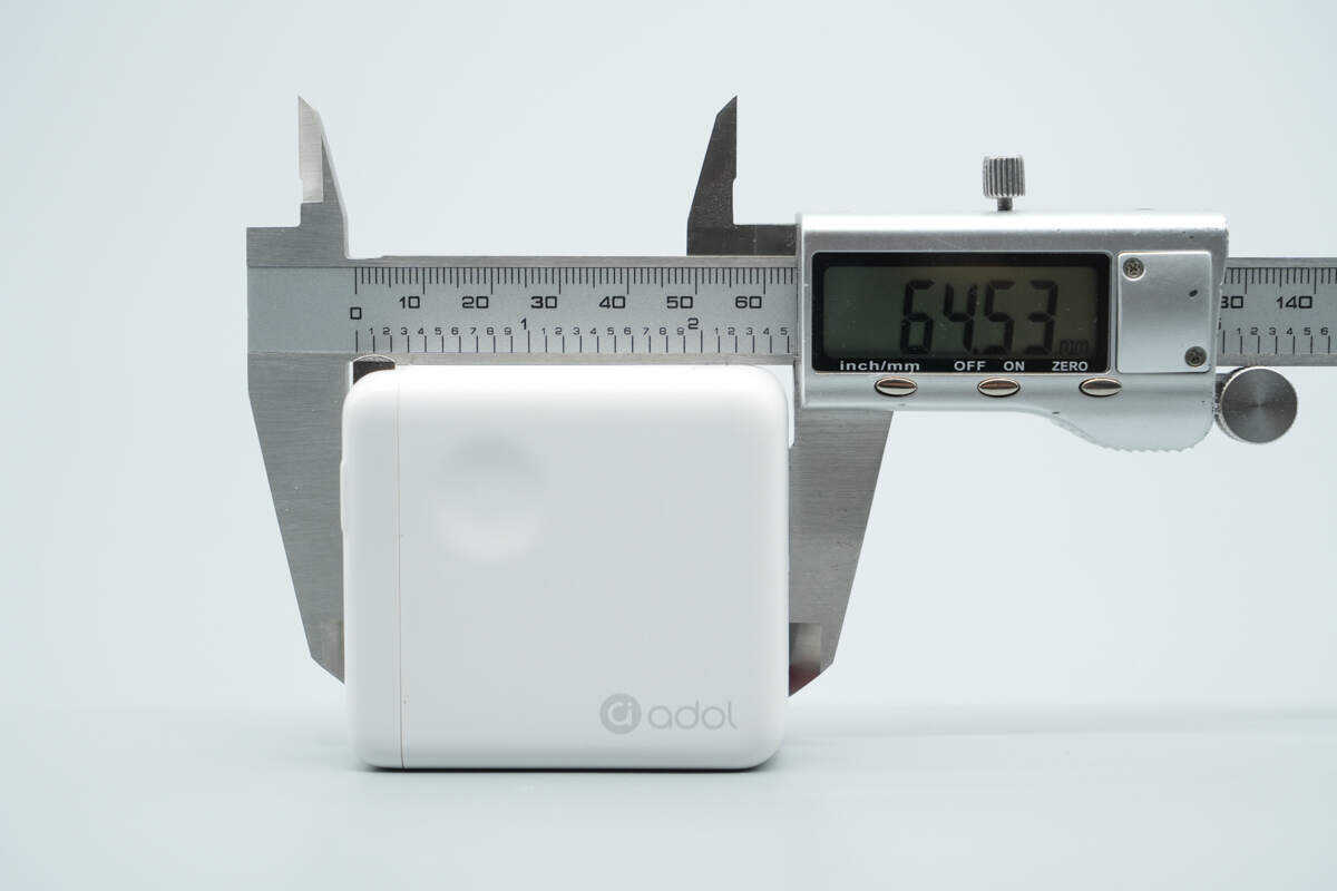
The length of the charger is about 64.53 mm (2.54 inches).
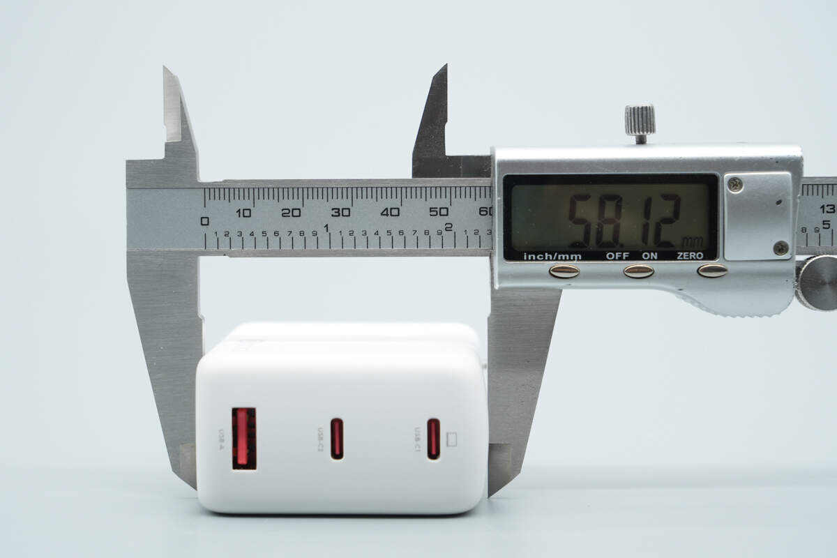
The width is about 58.12 mm (2.29 inches).
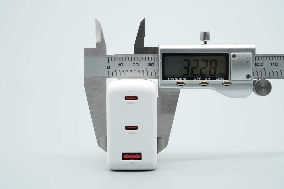
The thickness is about 32.28 mm (1.27 inches).
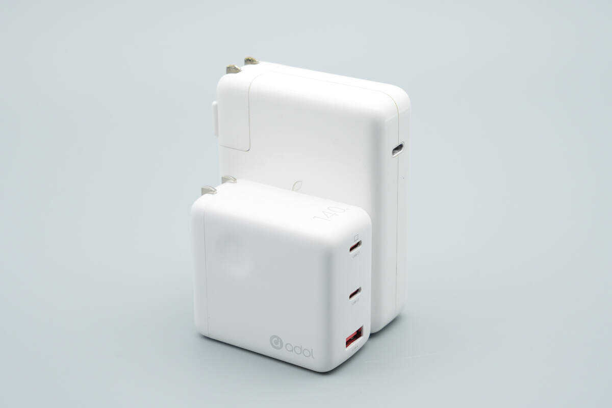
Compared with the Apple 140 W charger, its size advantage is obvious.
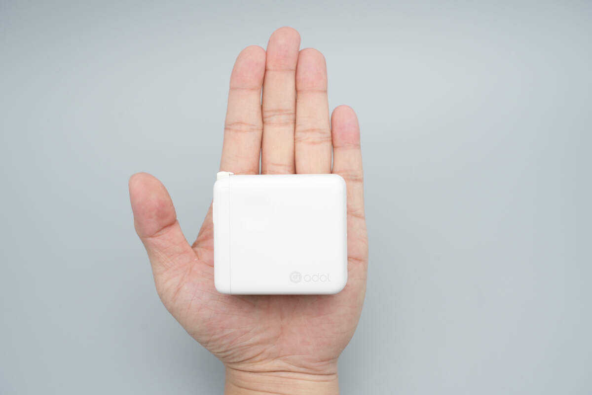
That's how big it is on the hand.

The weight is about 228 g (8.042 oz).
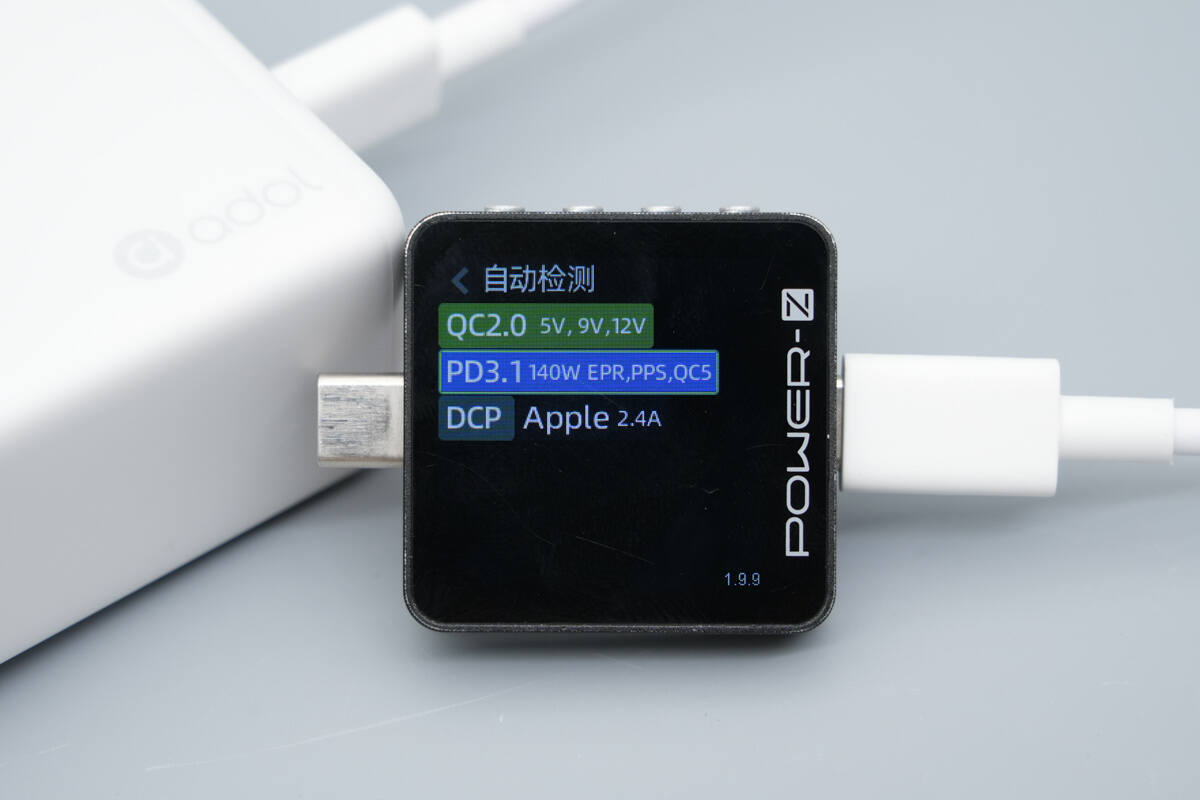
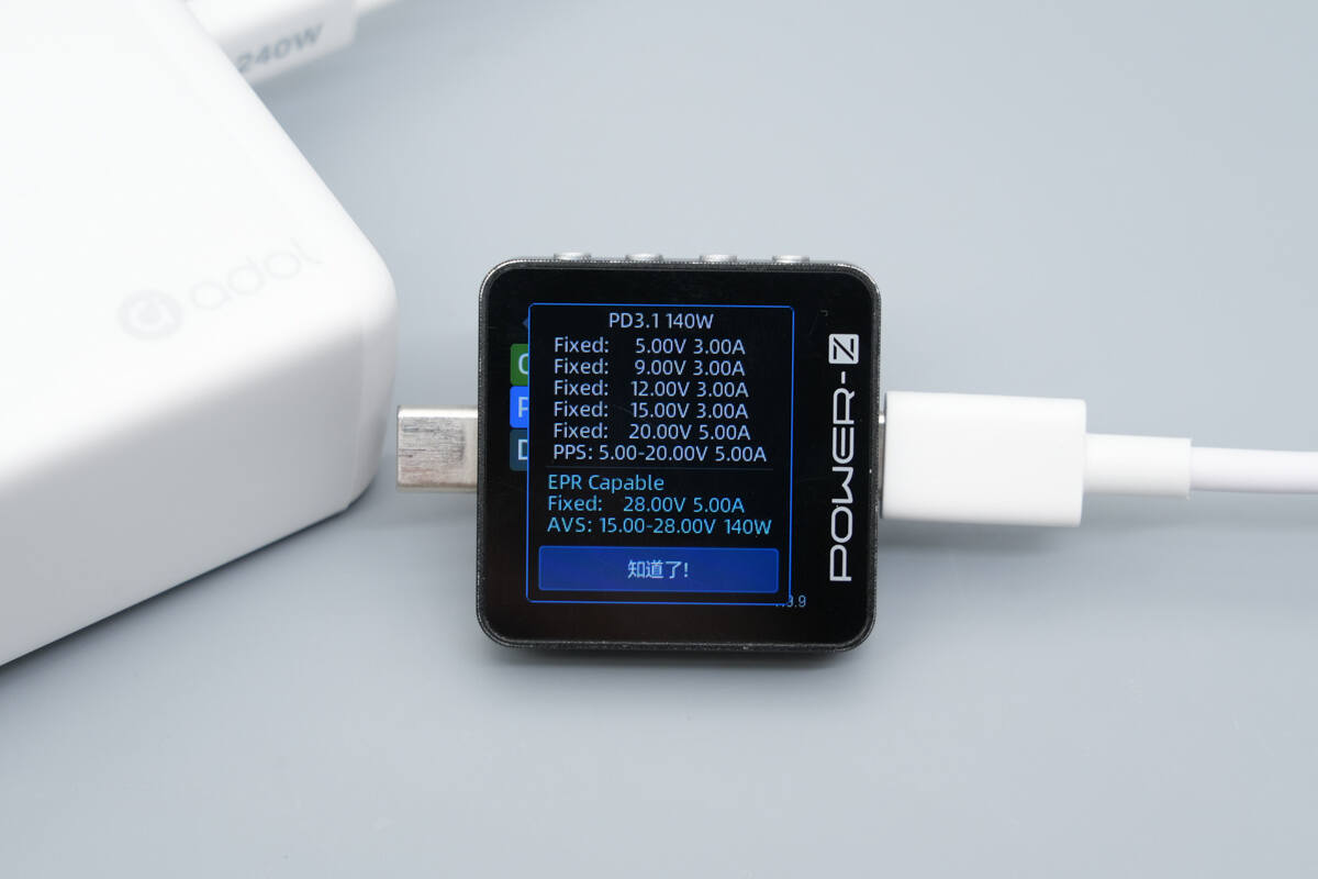
ChargerLAB POWER-Z KM003C shows that the USB-C1 supports QC2.0/5, PD3.1, PPS, DCP, and Apple 2.4A protocol.
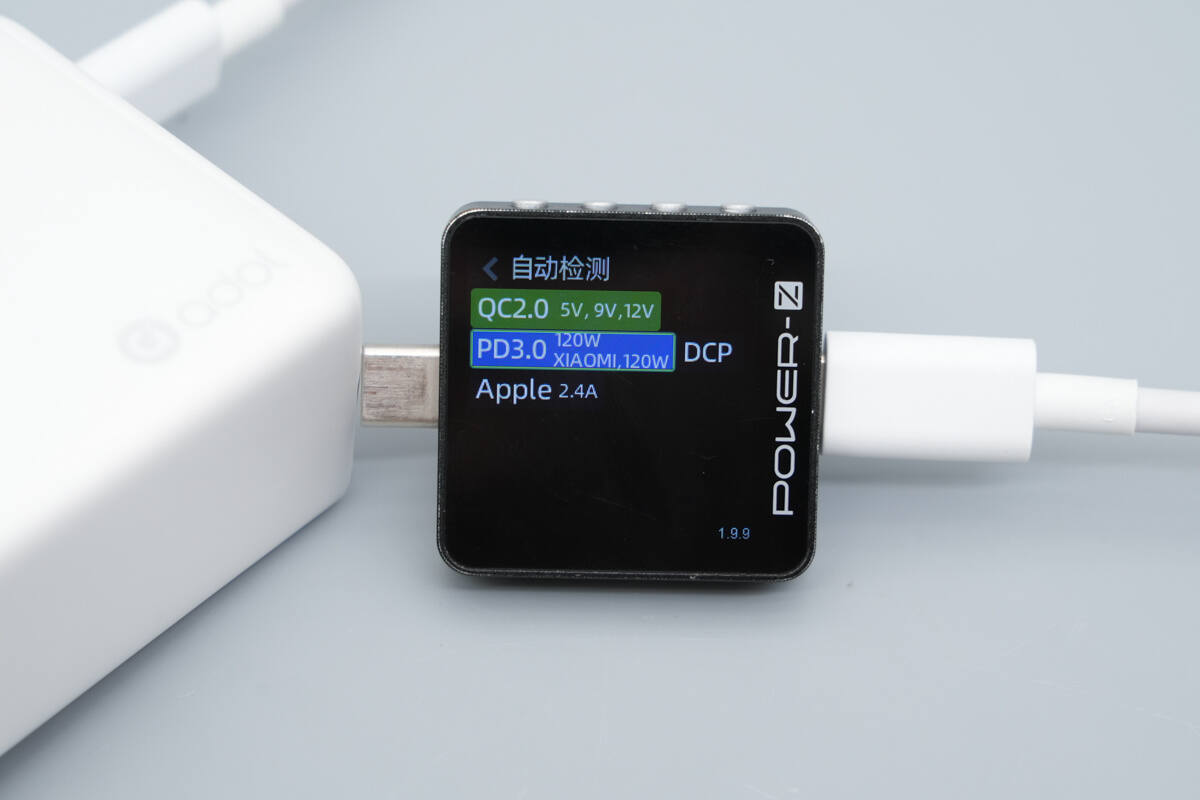
It also supports Xiaomi’s 120W Surge fast charging.
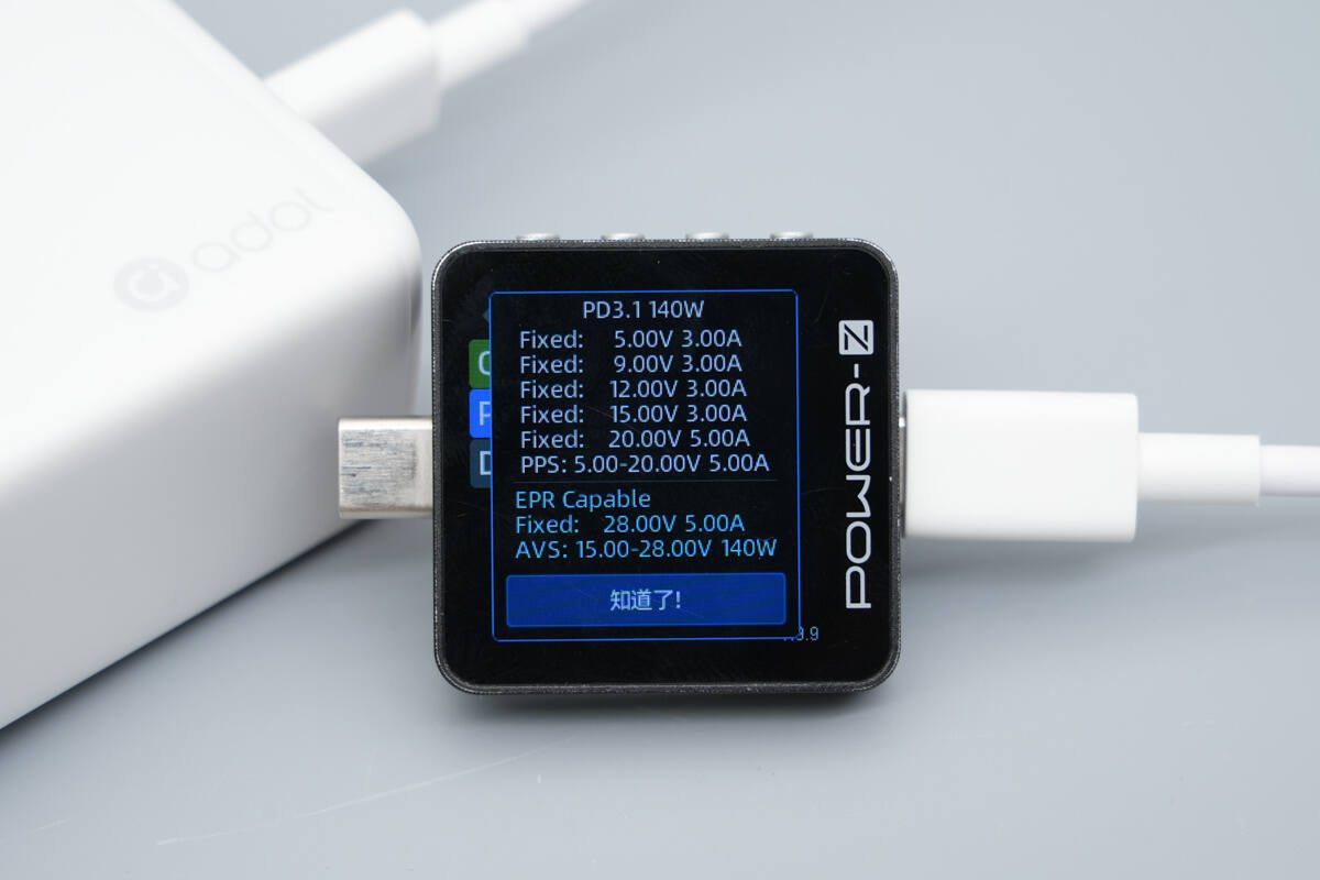
It has six fixed PDOs of 5V3A, 9V3A, 12V3A, 15V3A, 20V5A, as well as PPS ranges of 5–20V 5A and an AVS range of 15–28V up to 140W.
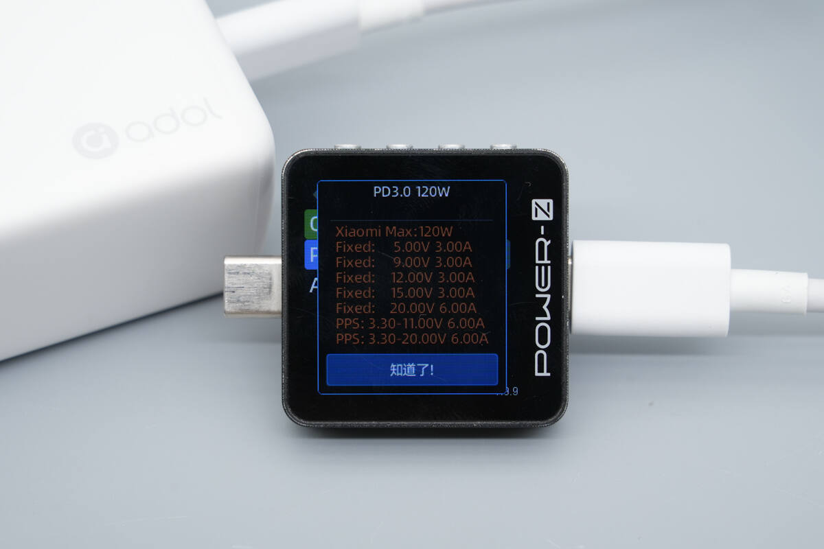
Testing confirmed that it supports two Xiaomi 120W Surge fast-charge private voltage levels: 3.3-11V6A and 3.3-20V6A.
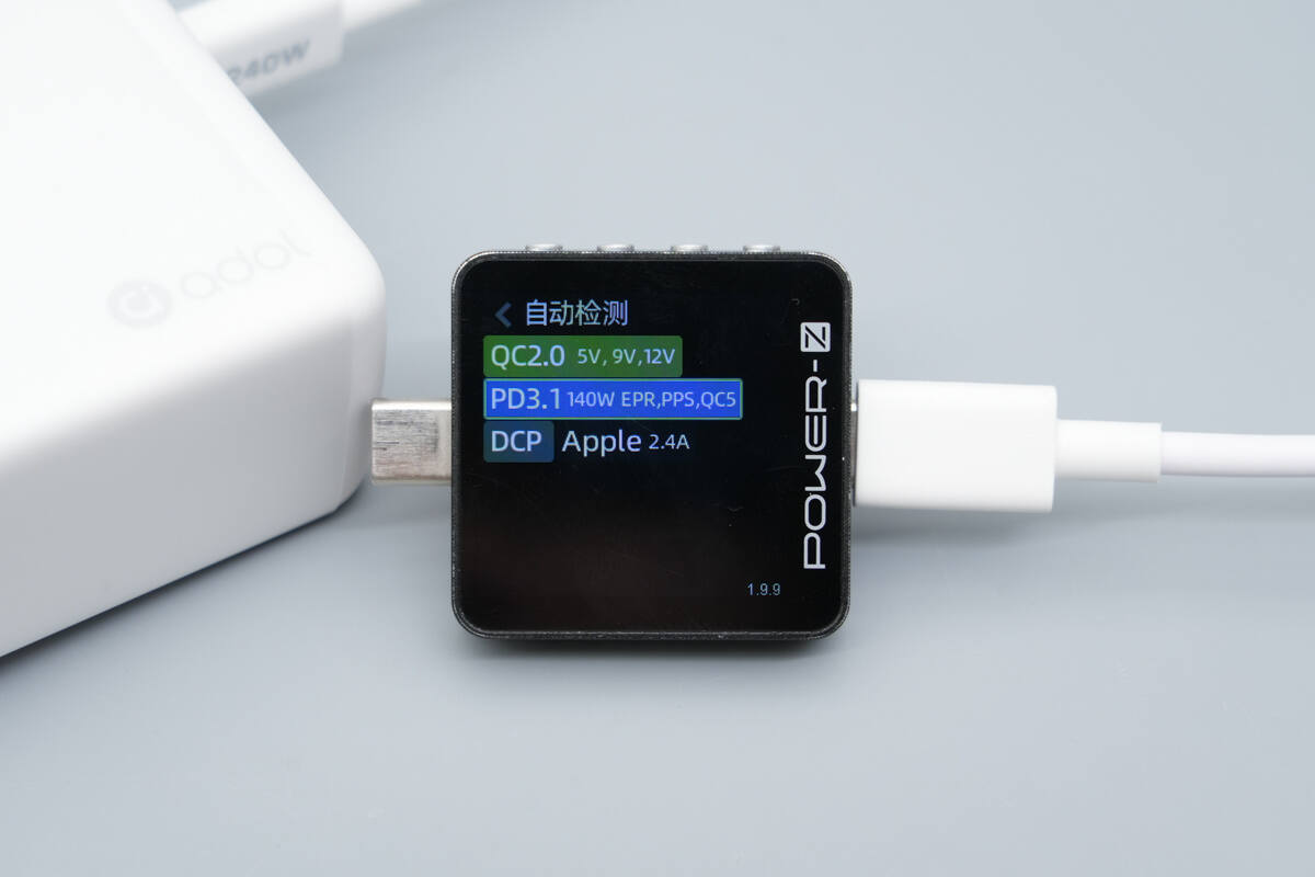
The USB-C2 supports QC2.0/5, PD3.1, PPS, DCP, and Apple 2.4A protocols.

It also supports Xiaomi’s 120W Surge fast charging.
The PDO reports show the same results as those of the USB-C1 port.
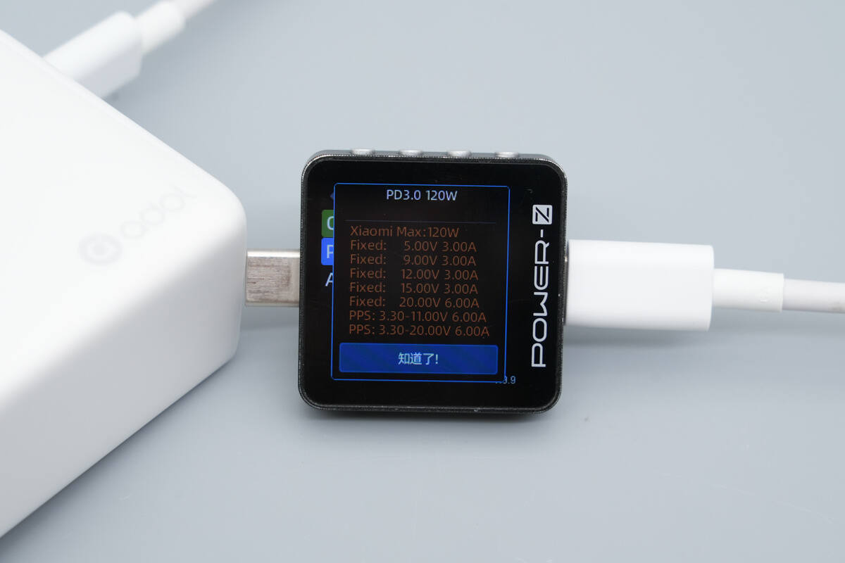
The USB-C2 port also supports two Xiaomi 120W Surge fast-charge levels: 3.3-11V6A and 3.3-20V6A.
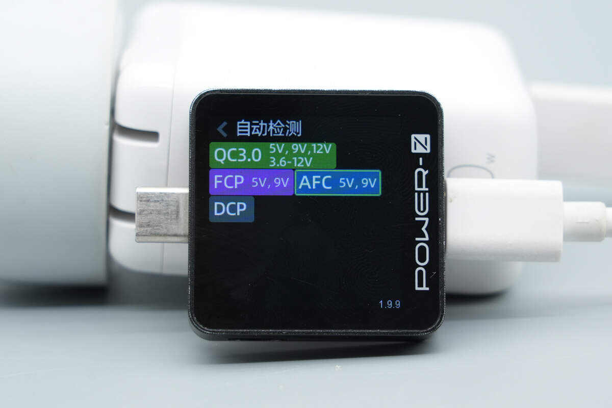
The USB-A supports QC3.0, FCP, AFC, and DCP charging protocols.
Teardown
Next, let's take it apart to see its internal components and structure.
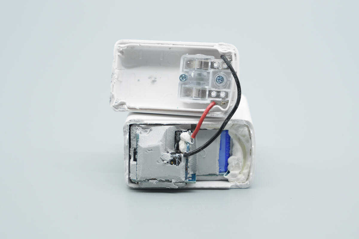
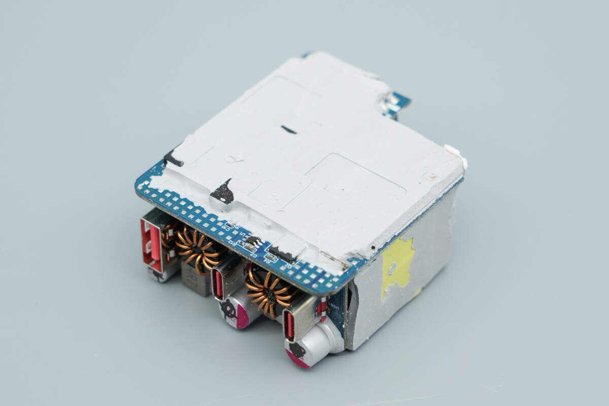
Remove the input-side housing. The PCBA module is secured with potting compound.
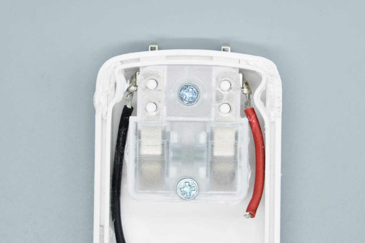
The plug is secured with a plastic plate and screws and connects to the PCBA via metal strips.

After removing the PCBA module, the inner side of the housing is seen to have graphite thermal pads and insulating tape.
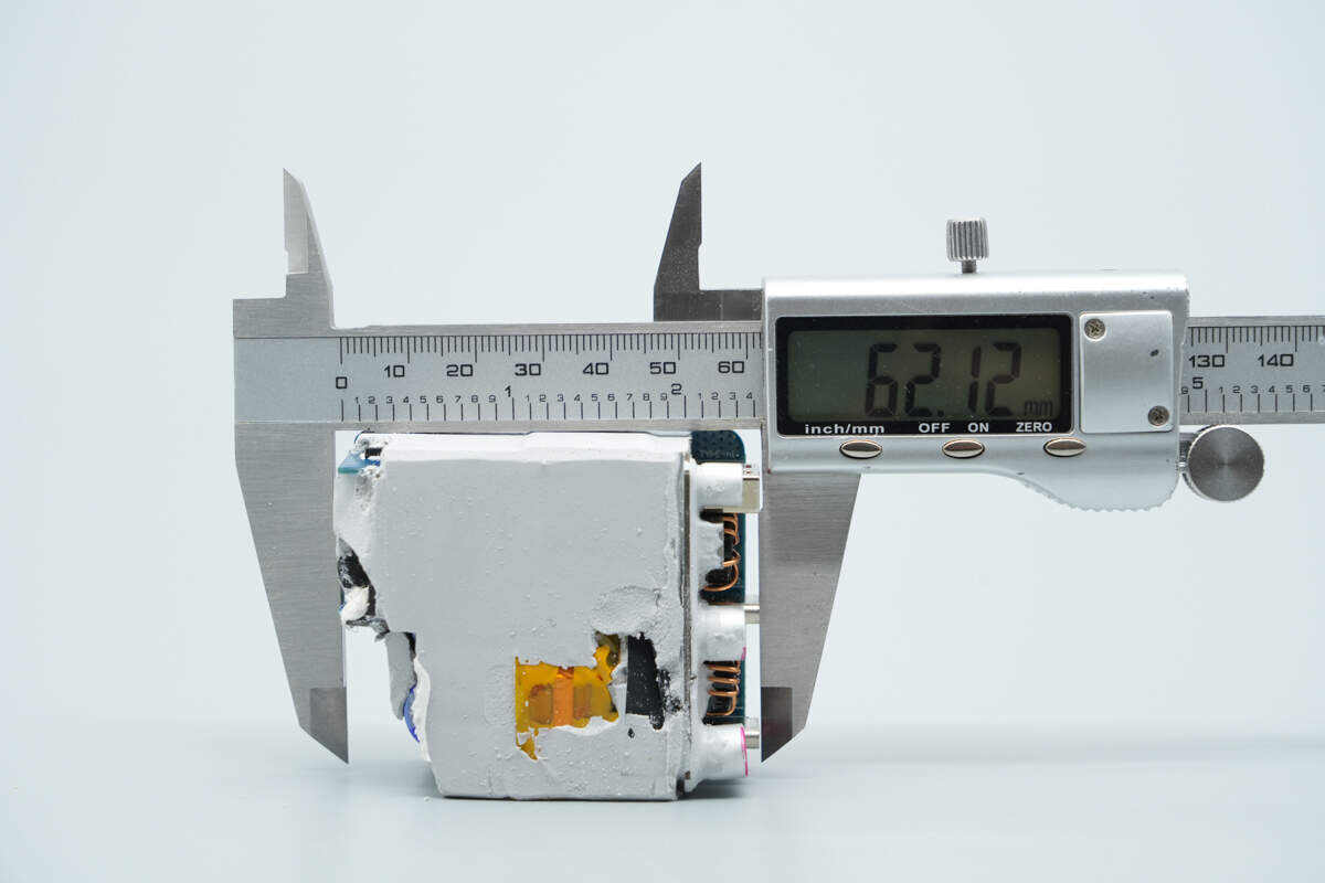
The length of the PCBA module is about 62.12 mm (2.45 inches).

The width is about 52.5 mm (2.067 inches).
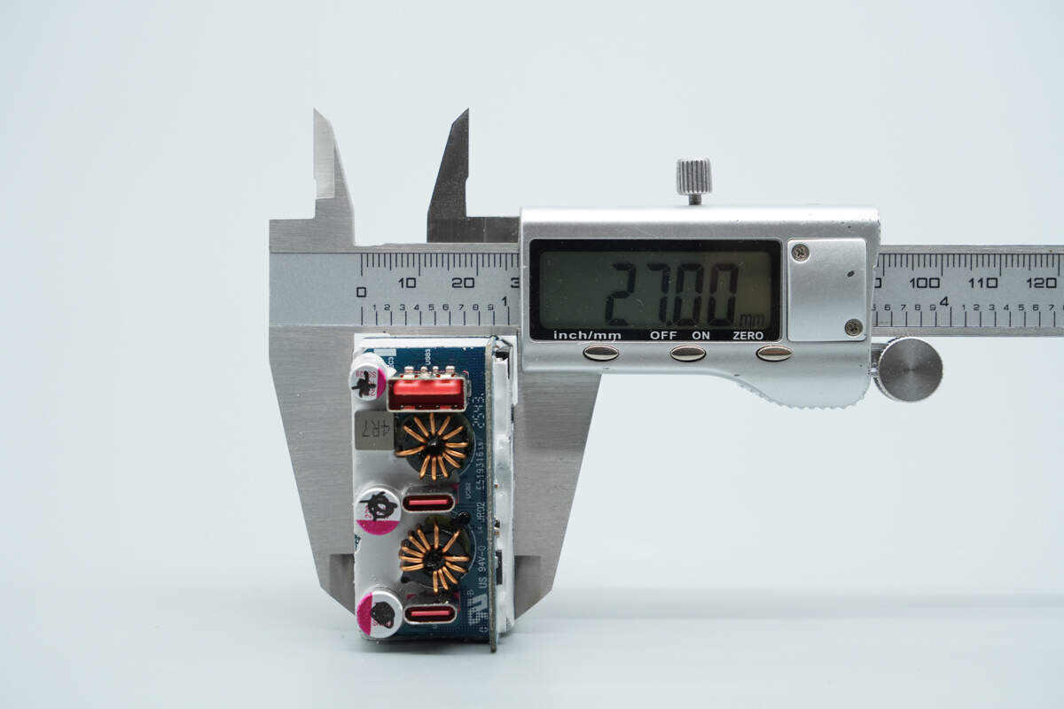
The thickness is about 27 mm (1.063 inches).
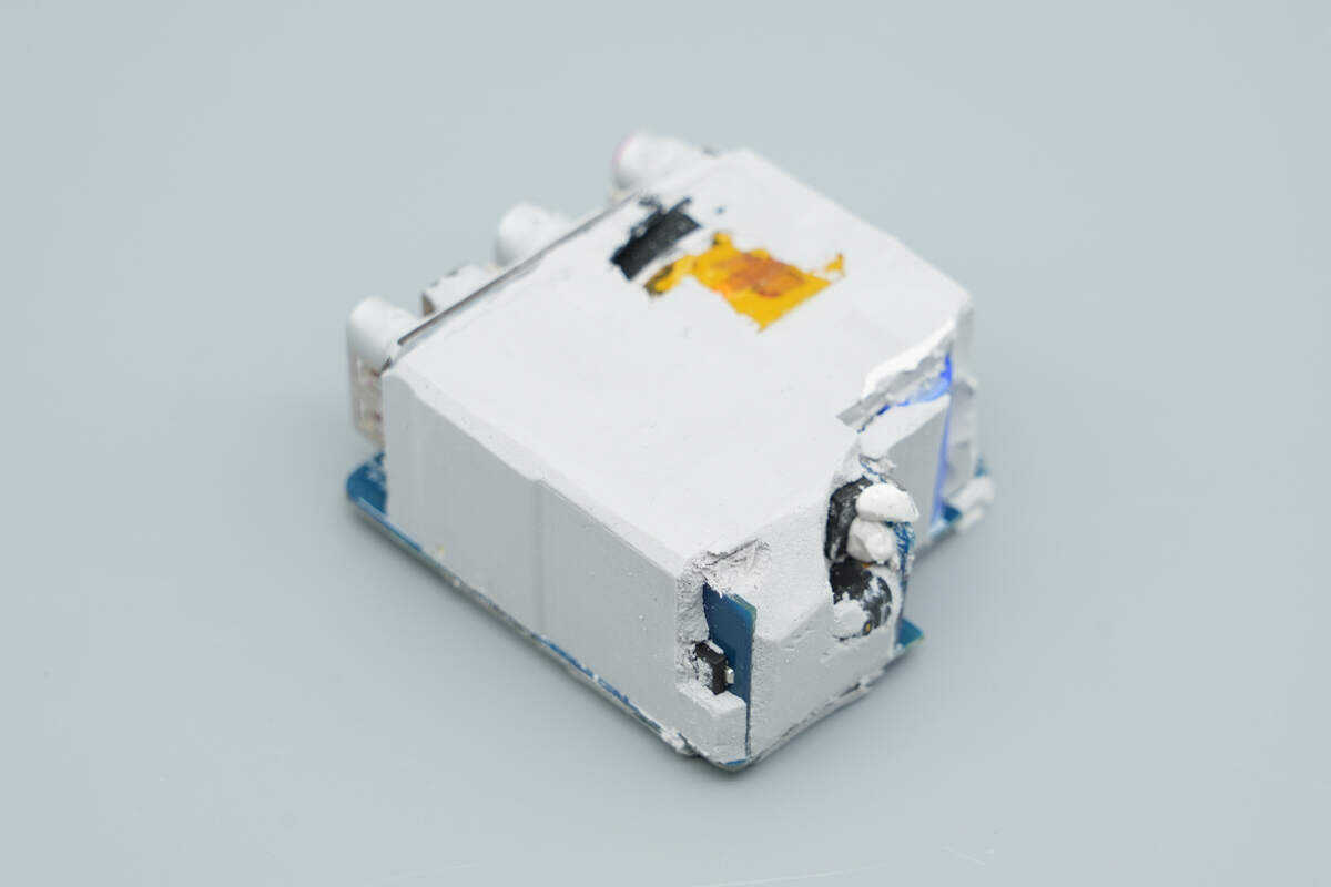
The PCBA module is potted to enhance overall thermal performance and durability.
The back side is also mostly covered with thermal adhesive.
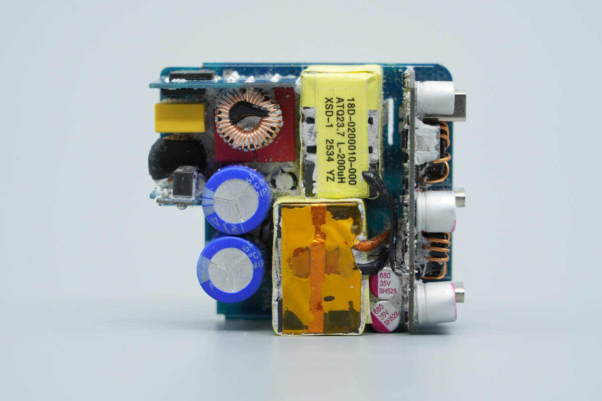
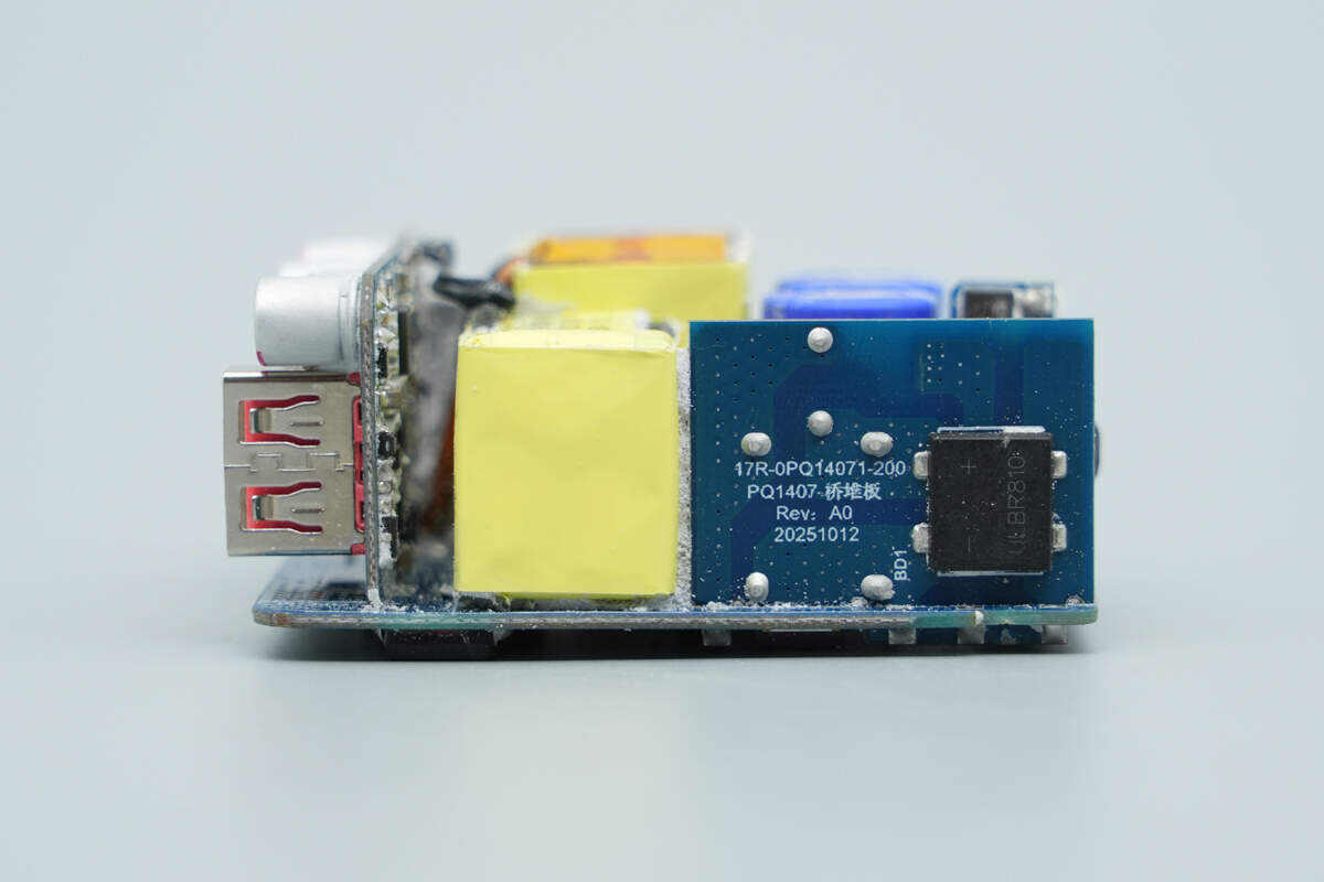
Clean off the thermal adhesive. The front of the module reveals three small PCBs soldered to it. The central area houses the PFC boost inductor, a capacitor that supplies power to the master control chip, the transformer, and other components.

On the back side, there are components including the PFC controller, PFC MOSFET, PFC rectifier, master control chip, optocoupler, SMD Y capacitors, synchronous rectifier controller, and synchronous rectifier.
The small PCB is soldered on this side.
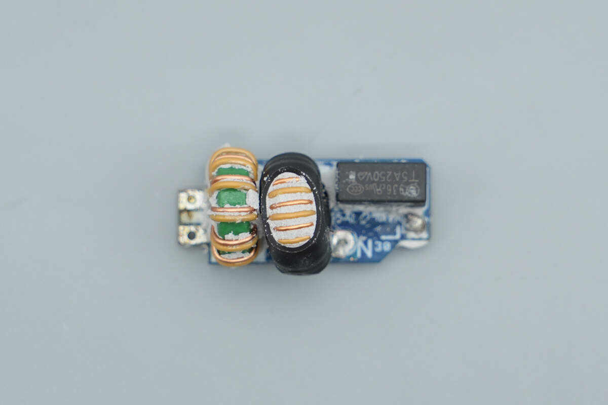
Remove the small PCB. The front side is equipped with a time-delay fuse and two common mode chokes.
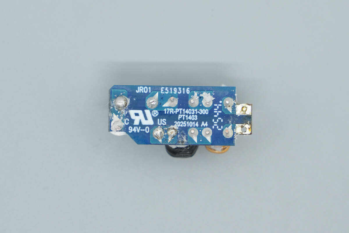
The back side has no components.
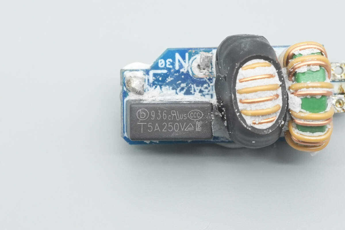
The time-delay fuse is from Betterfuse, marked “936,” and rated at 5A 250V.
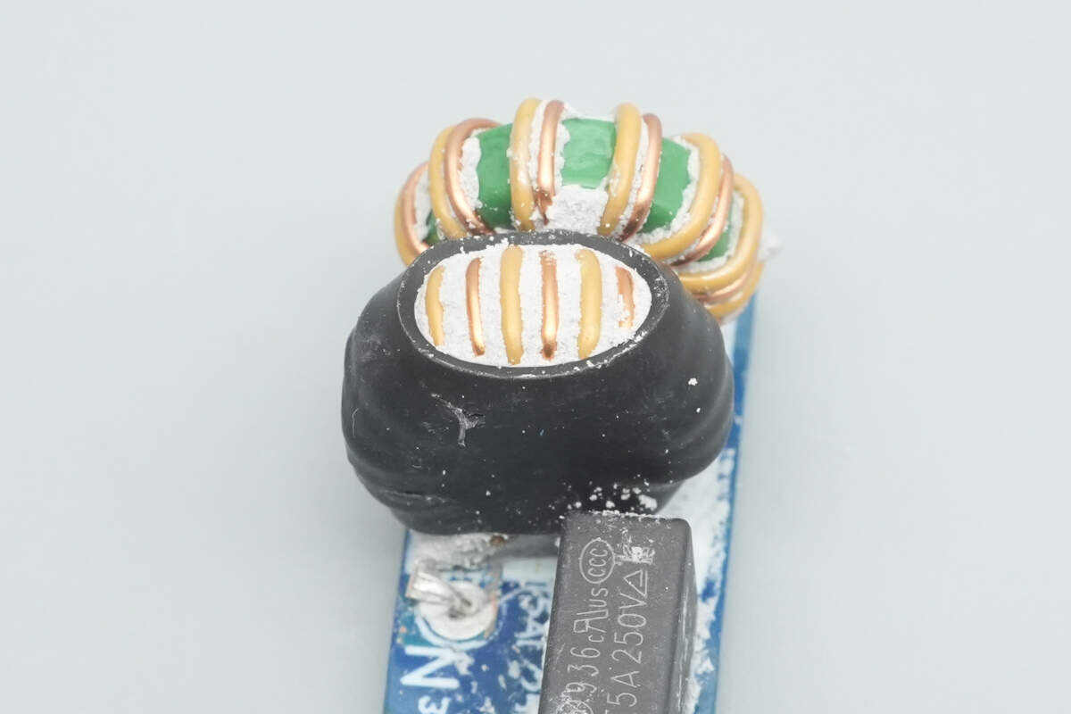
This common mode choke is insulated with a layer of heat-shrink tubing.
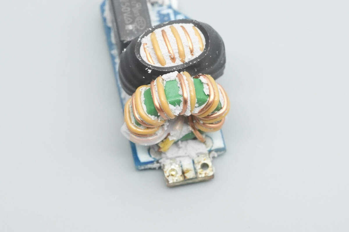
This is the second common mode choke, making a pair used to suppress EMI interference.
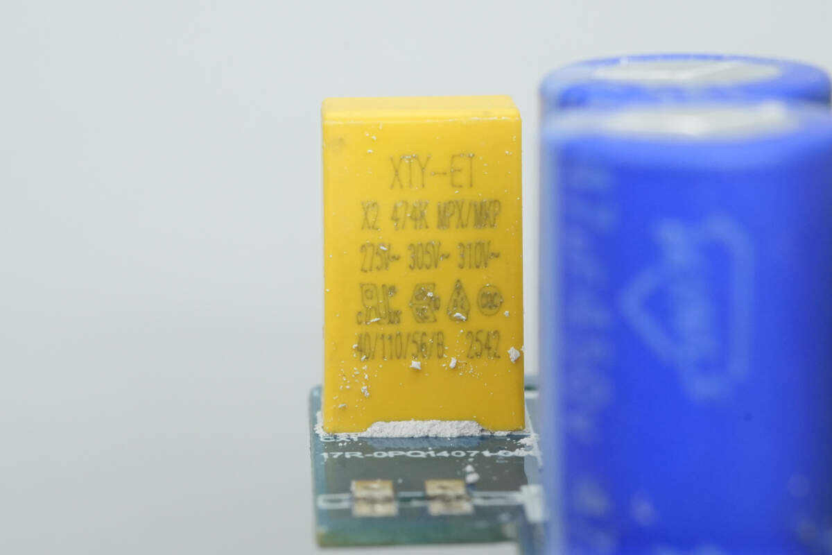
The safety X2 capacitor has a capacitance of 0.47 µF.
On this side of the module are the rectifier PCB and the PFC boost inductor. The back of the rectifier PCB is equipped with a bridge rectifier.
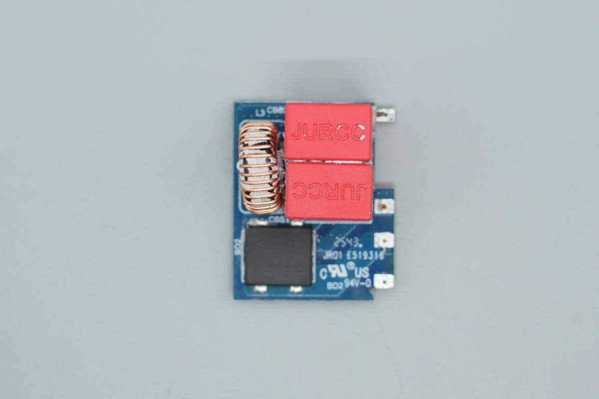
Remove the small PCB. The other side also contains a bridge rectifier, along with film capacitors and a filter inductor.
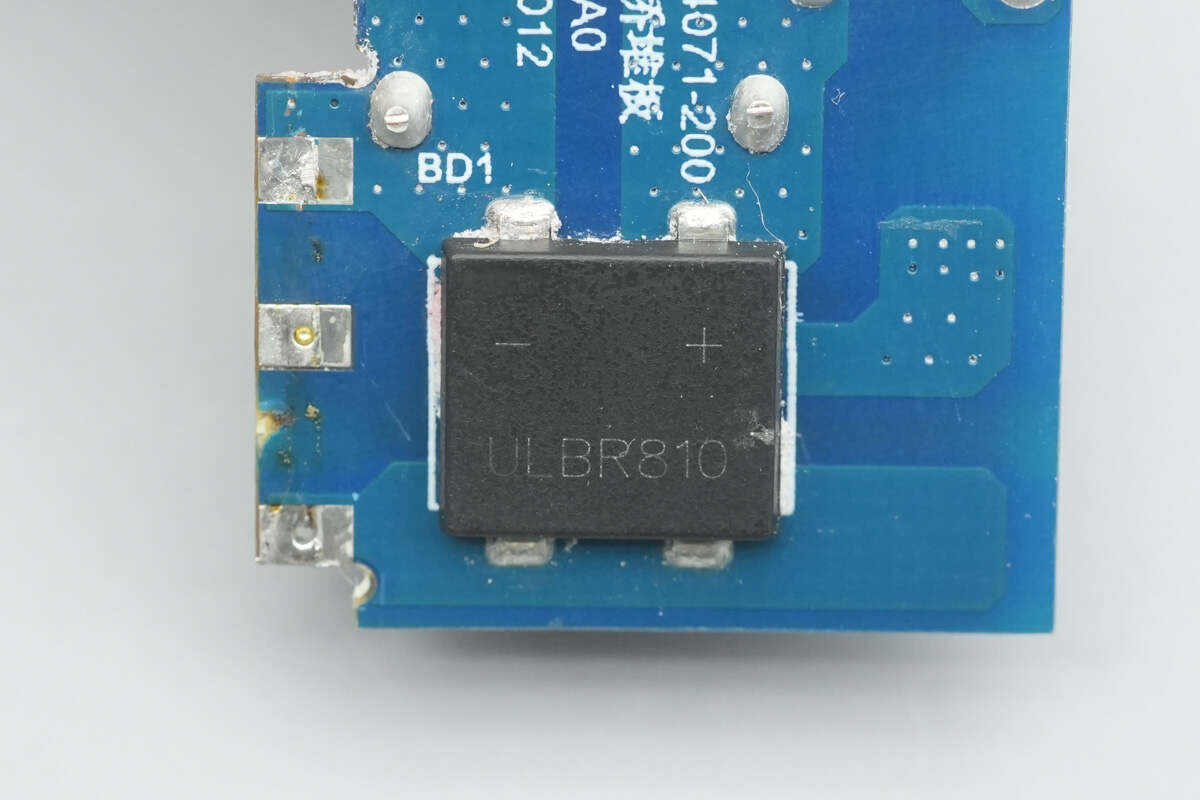
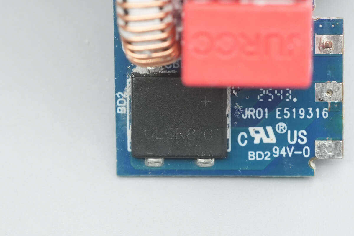
The bridge rectifier is from XH, model ULBR810, rated at 8A 1000V, and housed in a ULBF package.
The other bridge rectifier is the same.
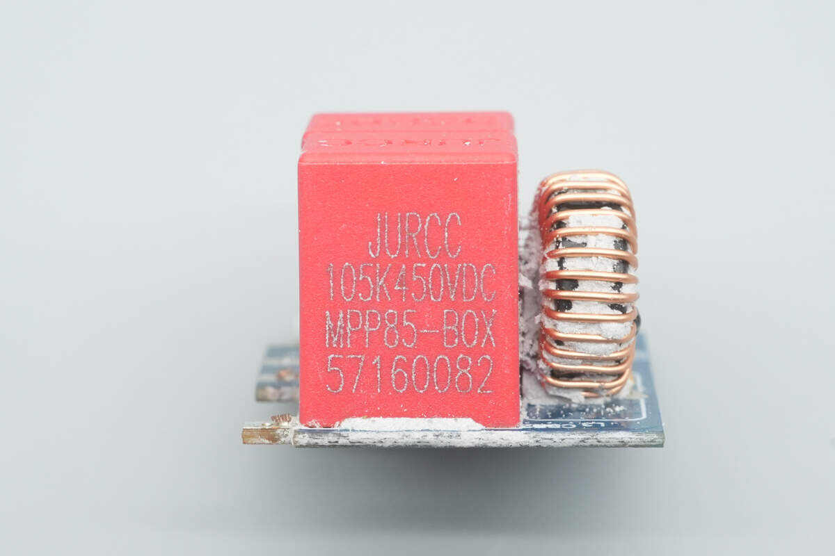
The two film capacitors are from JURCC, part of the MPP85-BOX series, each rated at 1 µF 450V.

Close-up of the filter inductor.
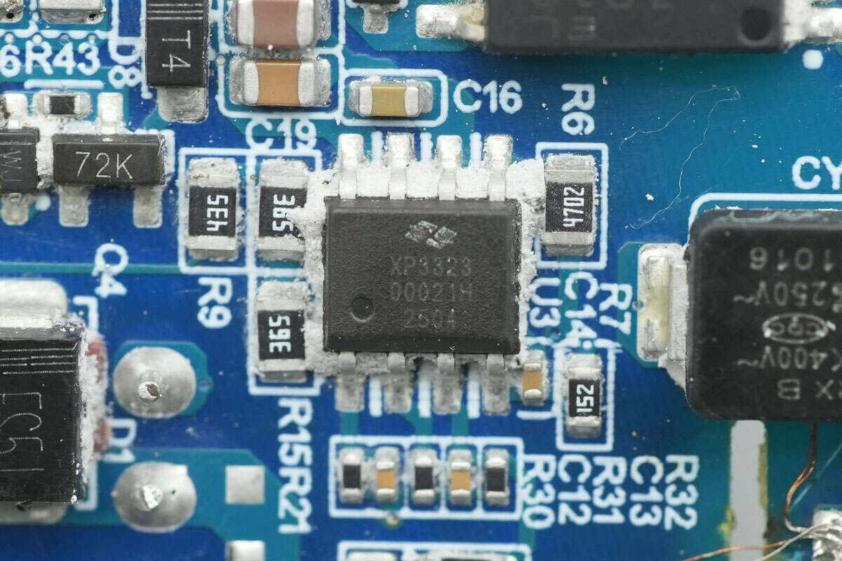
The PFC controller is from X-Signal, model XP3323. It operates in boundary mode, uses a patented digital power control algorithm, offers excellent dynamic performance and light-load PF/THD characteristics, and comes in an SOP8 package.
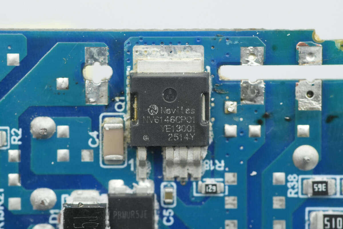
The PFC MOSFET is from Navitas, model NV6146C. It is a Navitas GaNSlim GaN power device with an integrated 700V rating and 170 mΩ high-performance enhancement-mode GaN FET. It features an integrated gate driver and lossless current sensing, supports over-temperature protection, and is suitable for fast charging, wireless power transfer, LED lighting, solar microinverters, server power supplies, and other applications. The device comes in a DPAK-4L package.

Close-up of the PFC boost inductor.

The PFC rectifier is from PY, model PBMUR5JE. It is an ultra-fast recovery diode rated at 600V 5A and comes in a PS-277B package.
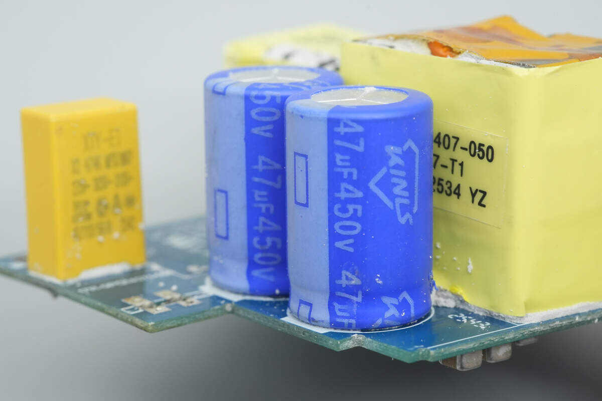
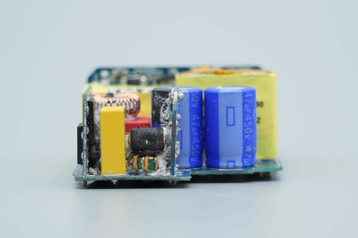
The electrolytic capacitors are from KINLS, each rated at 450V 47 µF.
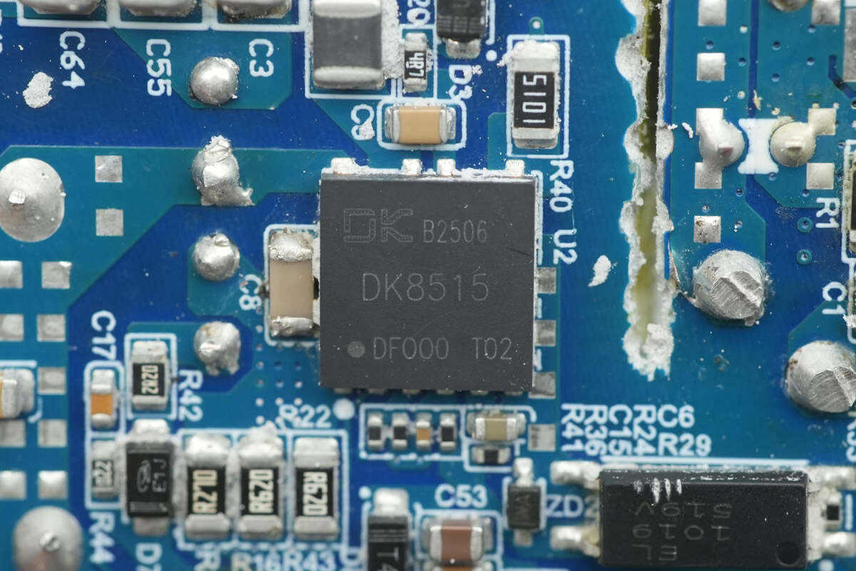
The master control chip is from DONGKE, model DK8515. It is an AC-DC power switching chip based on an asymmetric half-bridge architecture, integrating two GaN power devices. The DK8515 achieves ZVS on the primary-side power transistors and ZCS on the secondary-side rectifiers over a wide load range, improving overall power supply efficiency. The soft-switching operation also reduces stress on the power devices, lowers switching losses, and improves EMI performance.
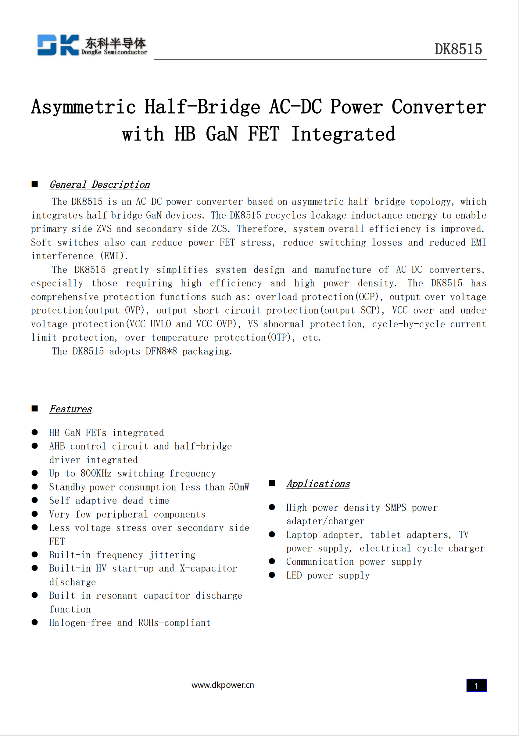
The DK8515 requires minimal external components, greatly simplifying the design and manufacturing of AC-DC converters, especially for products that demand high conversion efficiency and high power density. It also features comprehensive protection functions, including overload protection, output over-voltage protection, output short-circuit protection, VCC over/under-voltage protection, VS pin fault protection, primary-side overcurrent protection, and over-temperature protection.
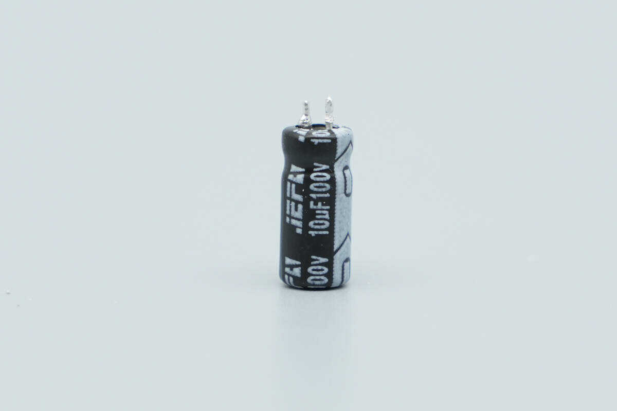
The capacitor supplying power to the master control chip is from JEFA, rated at 100V 10 µF.
Close-up of the transformer.
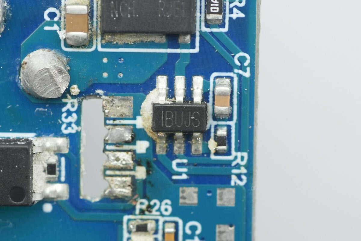
The synchronous rectifier controller is from MPS, marked with IBUJS, model MP6951. It is a newly released MPS chip that supports DCM, CCM, QR, and ZVS operating modes. It also supports ACF active clamp flyback and HFB hybrid flyback, with an operating frequency up to 1 MHz. The controller can drive GaN synchronous rectifiers and is suitable for both high-side and low-side applications. It comes in a TSOT23-6 package.

The synchronous rectifier is from PY, model PWC038N10ES. It is an N‑MOSFET with a 100V rating and 3 mΩ on-resistance, housed in a DFN 5×6 package.
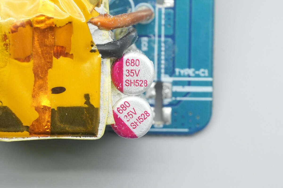
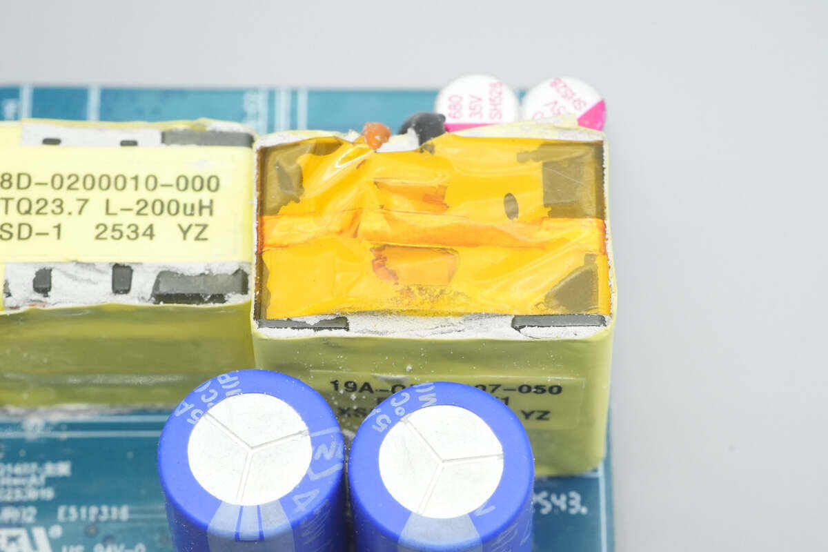
The solid capacitors used for output filtering are each rated at 35V 680 µF.
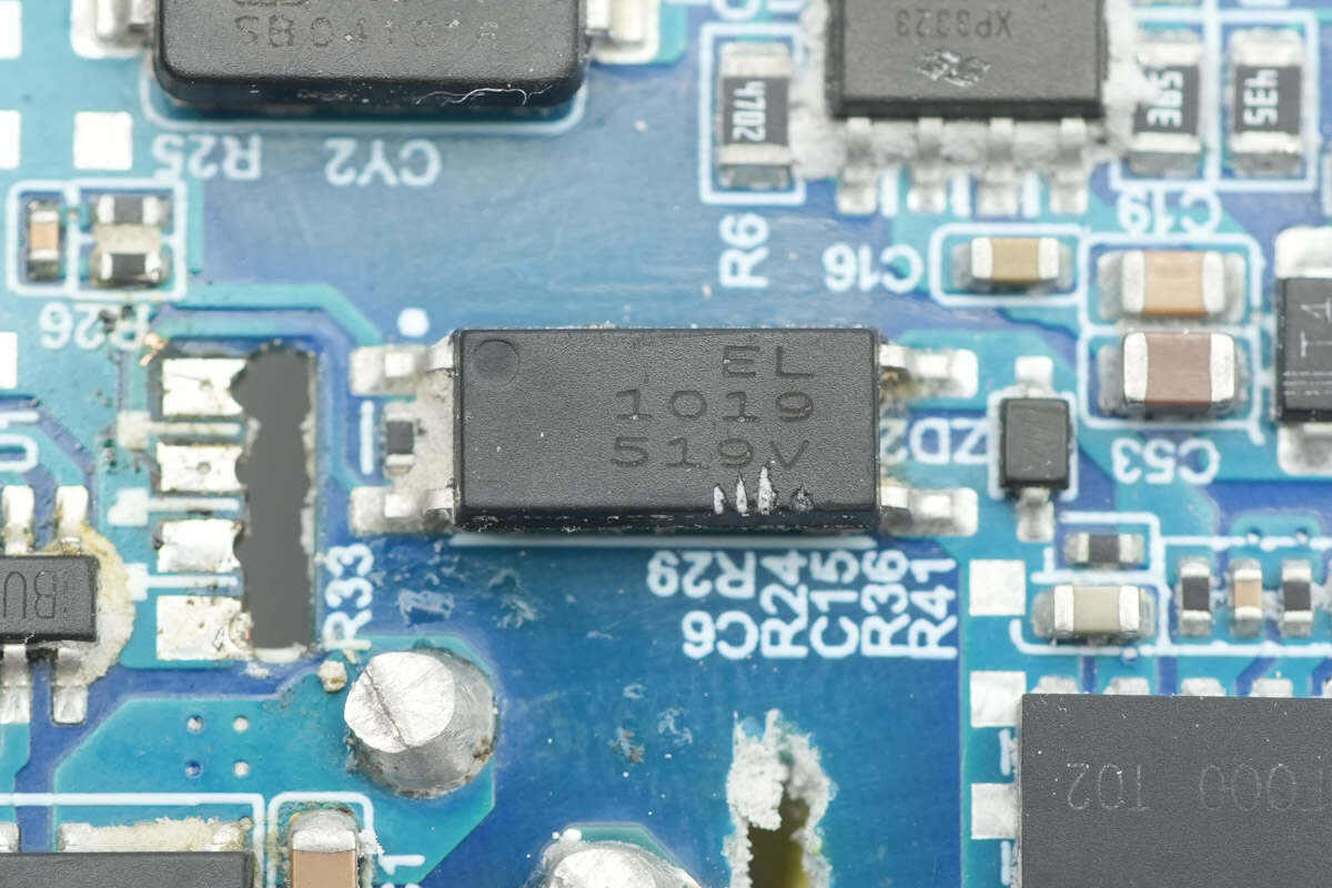
The Everlight EL1019 optocoupler is used for output voltage feedback.
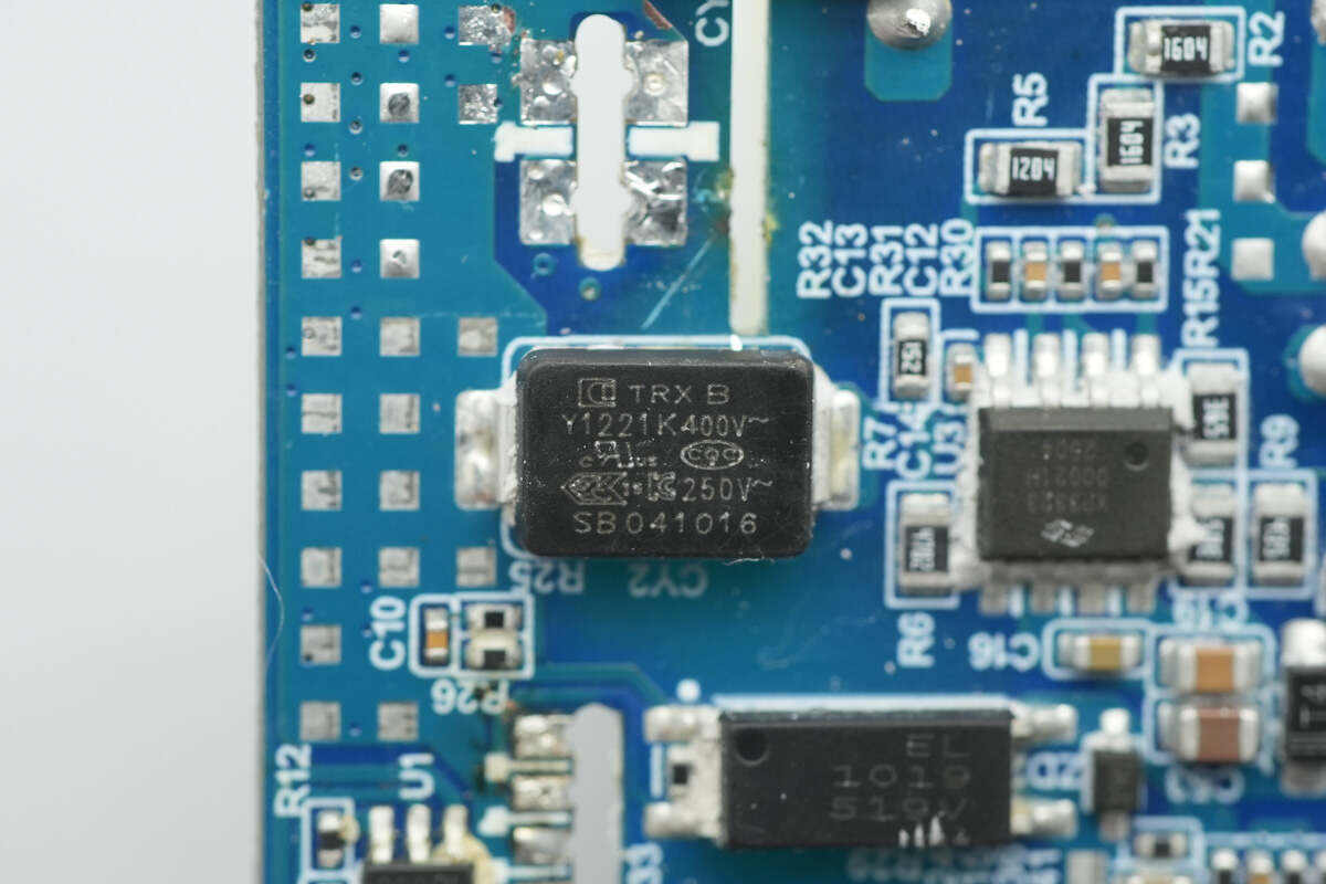
The SMD Y capacitor is from TRX, part number TMY1221K. Its compact size and light weight make it well-suited for high-density power products such as GaN fast chargers.

The other SMD Y capacitor is also from TRX, with part number TMY1471K.
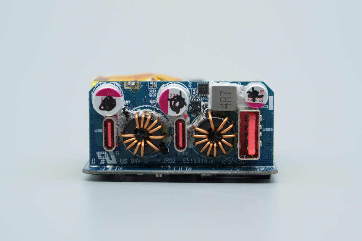
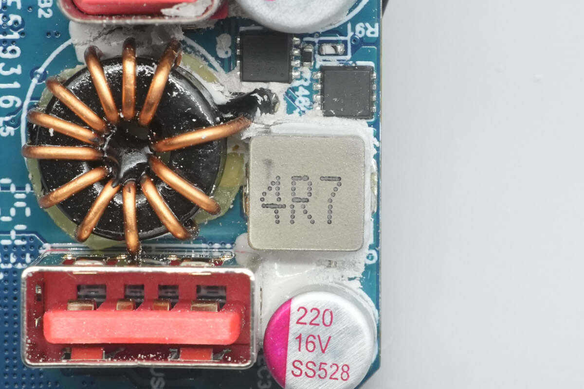
A PCB is soldered at the output side.
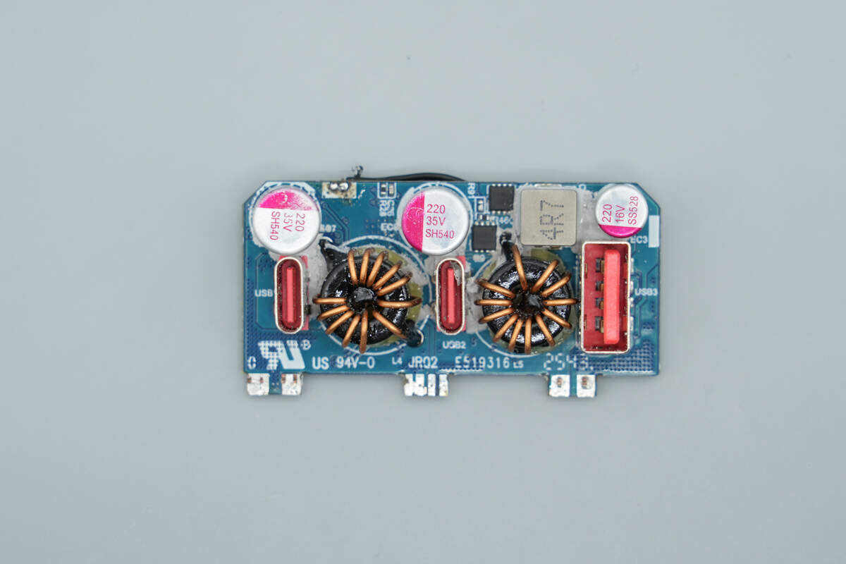
The front side features buck inductors, solid capacitors, and VBUS MOSFETs.
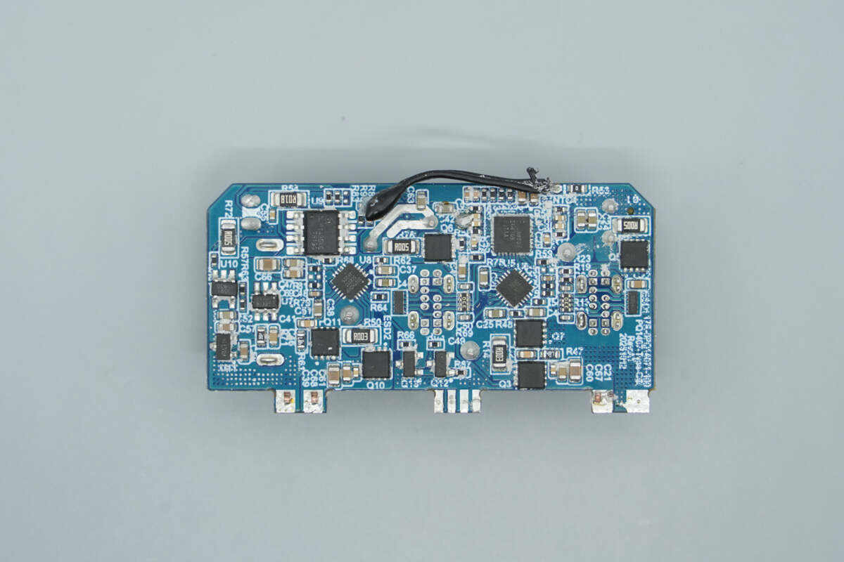
The back side contains synchronous buck controllers, a synchronous buck converter, synchronous buck MOSFETs, protocol chips, and VBUS MOSFETs.
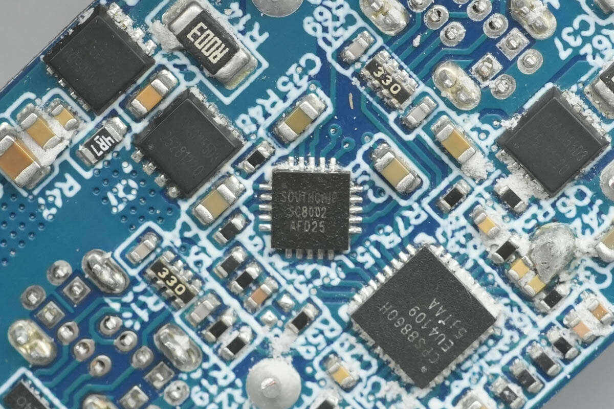
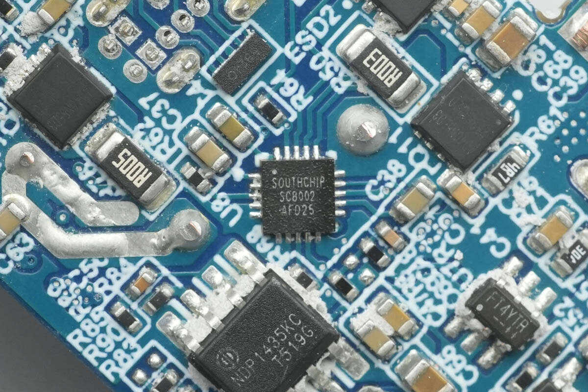
The synchronous buck controller for the USB-C1 port is from SouthChip, model SC8002. It accepts an input voltage from 4.6V to 36V and can be configured for either single-output or dual-output operation. The SC8002 allows the output voltage to be set to a fixed 5V or a custom voltage via resistor programming. It also provides high-precision output current limiting. When either of the two output channels reaches the set current limit, the SC8002 enters constant-current (CC) mode. The total output power can be set via resistors, enabling constant-power control.
The SC8002 allows frequency adjustment and the selection of either PWM or PFM operation. With a minimal BOM, it can deliver maximum functionality for various user applications. The SC8002 also supports comprehensive protection features, including under-voltage protection, over-voltage protection, short-circuit protection with auto-restart, and over-temperature protection. Its main applications include automotive chargers, multi-port adapters, hubs, and industrial voltage conversion.
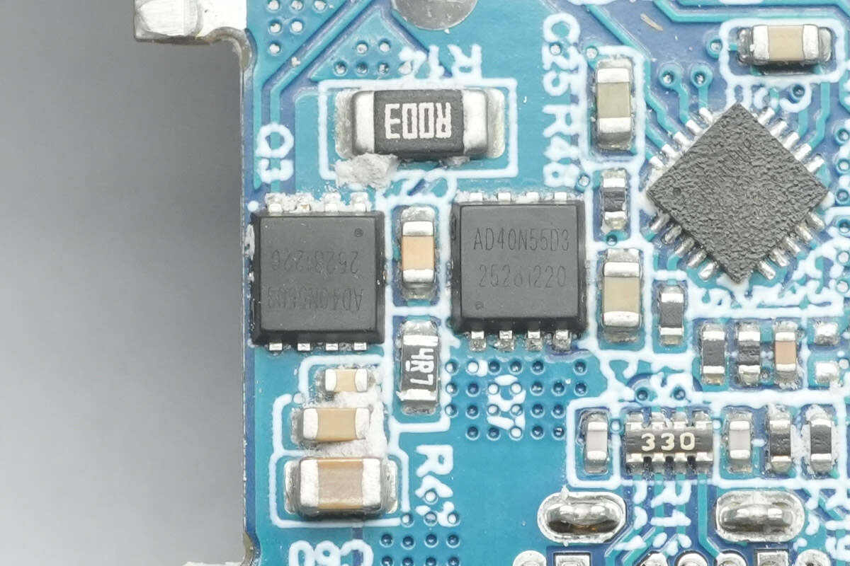
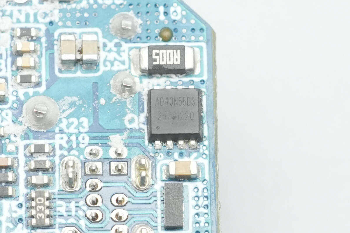
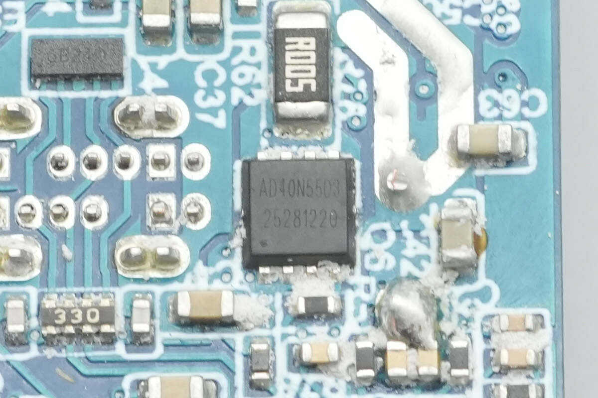
The two accompanying synchronous buck MOSFETs are from Adamant, model AD40N55D3. They are N‑MOSFETs with a 40V rating and 4.5 mΩ on-resistance, housed in a PDFN 3×3 package.

The bottom of the buck inductor is supported with a bakelite board and reinforced with potting compound.
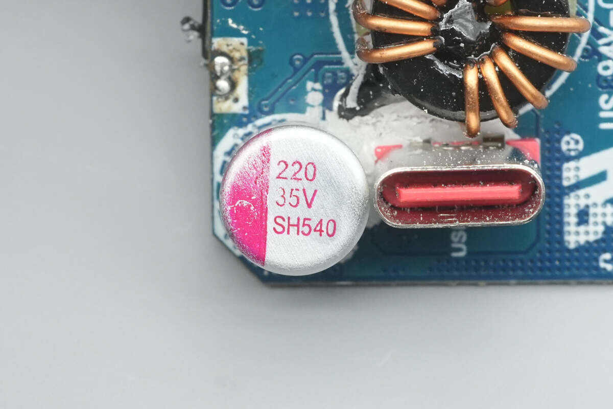
This solid capacitor is rated at 35V 220 µF.
The synchronous buck controller for the secondary buck output of the USB-C2 port is also the SouthChip SC8002.

The two accompanying synchronous buck MOSFETs are also Adamant AD40N55D3.

Close-up of the buck inductor.

The solid capacitor is rated at 35V 220 µF.

The protocol chips for the two USB-C ports are from CPS, model CPS8806H. This is a highly integrated dual-port charging chip that supports PD 3.1, PPS, QC 2.0/3.0/3+, UFCS, SCPA/B, AFC, and other fast-charging protocols. It features dual fast-charging outputs, intelligent dual-port management logic, and dynamic power allocation, allowing the construction of an efficient, high-quality multi-protocol dual-port charging solution with minimal external components.
Here is the information about CPS CPS8806H.
The VBUS MOSFET for the USB-C1 port is an Adamant AD40N55D3.
The VBUS MOSFET for the USB-C2 port is also an Adamant AD40N55D3.

The synchronous buck converter for the USB-A port is from NDP, model NDP1435KC. It is a high-efficiency, monolithic synchronous step-down DC/DC converter that uses a constant-frequency average-current-mode control architecture. It can deliver up to 3.5A of continuous load current and provides excellent line and load regulation.
The NDP1435KC operates over an input voltage range of 7–38V and supports an adjustable output voltage from 1–25V. It features built-in short-circuit and thermal protection circuits to enhance system reliability. The internal soft-start function prevents input surge currents during startup. Housed in an SOP8 package, the chip requires minimal external components to operate and comes with a comprehensive set of protection features, further improving overall system robustness.
Close-up of a 4.7μH buck inductor.

The solid capacitor is rated at 16V 220 µF.
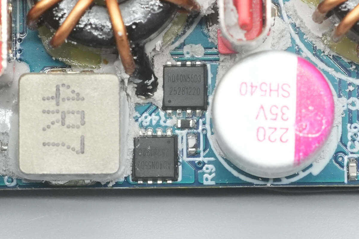
The two VBUS MOSFETs are Adamant AD40N55D3.

The protocol chip for the USB-A port is from JADARD, marked with FT4, model FP6601Q. It is widely used and supports QC 2.0/3.0 and Huawei FCP fast-charging protocols.

Well, those are all components of the ASUS Adol 140W GaN Quick Charger.
Summary of ChargerLAB
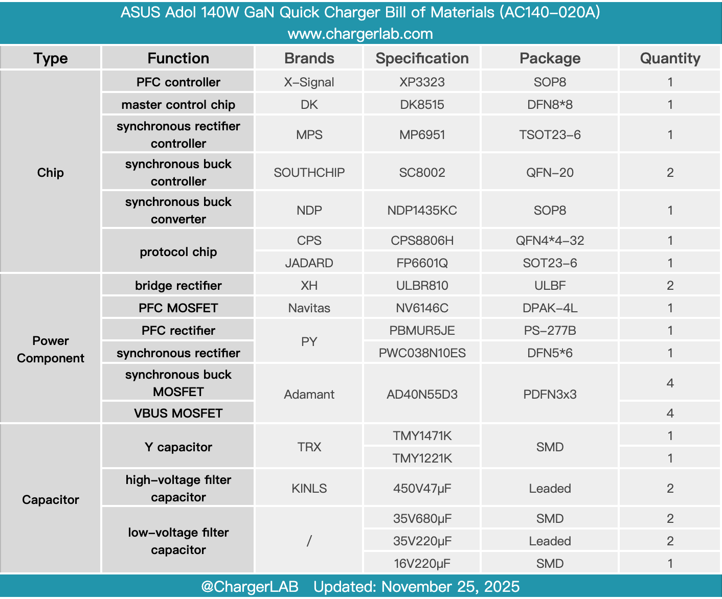
Here is the component list of the ASUS Adol 140W GaN Quick Charger for your convenience.
It features foldable pins, continuing the design language of the previously teardown 100W version. It is compatible with fast-charging protocols such as PD 3.1, PPS, AFC, and FCP, and also supports Xiaomi 100W/120W Surge Fast Charge, meeting users’ fast-charging needs.
After taking it apart, we found that the power supply uses a PFC+AHB high-efficiency topology composed of the X-Signal PFC controller XP3323 and the DONGKE DK8710BD integrated GaN chip solution. The three output buck circuits employ SouthChip SC8002 and NDP NDP1435KC buck designs, with the CPS CPS8806H protocol chip controlling the outputs of the two USB-C ports.
Thanks to the CPS CPS8806H protocol chip, the two USB-C ports achieve strong output performance and support dynamic power allocation, while also helping to simplify the external circuitry and reduce design complexity. The charger continues to use a potting process to enhance overall thermal performance and impact resistance, and the materials and build quality are reliable.
Related Articles:
1. Teardown of MIIIW 140W GaN Charger CA514 Pro (iCA1404)
2. Teardown of IM Motors 50W In-Car Pre-installed Wireless Charging Module
3. Teardown of BYD 50W In-Car Pre-installed Wireless Charging Module